1
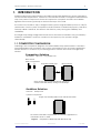
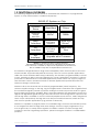
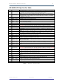
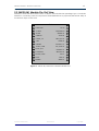
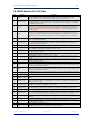
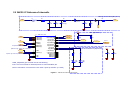
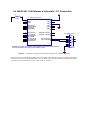
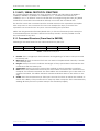
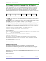
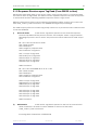
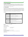
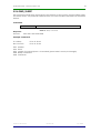
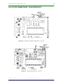
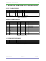
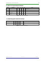
SM125
SM125-IC 125 KHz RFID Chip
SM125-M1 125 KHz RFID Module
Firmware V3.0 DATA SHEET
Single-Chip including microcontroller, RF circuit and Antenna Driver results in
World’s lowest count and smallest RFID Reader.
Available as IC (Integrated Circuit) or Module.
Requires only antenna and power supply to function
Automatically demodulate and decode RF signal and make the actual tag
data ready. No need to know about complicated RFID subject.
Supports Atmel / Temic T55xx and EM4102(Unique) tags
Supports Manchester RF/64, Manchester RF/32 modulation
5V or 3.3V Operation
Sleep Operation
UART Interface up to 115200bps – I2C Interface up to 400 KHz
Custom defined General Purpose I/O
Supports Wiegand 26-Bit output
Firmware Upgradeable for customer specific applications
SonMicro Electronics
Revision A.4
July, 2008
2
SM125 Datasheet – Firmware Version 3.0x
1.
INTRODUCTION
4
1.1 COMPETITOR COMPARISION
4
1.2 FUNCTIONAL OVERVIEW
1.2.1 Supported Modulation and Tag Types
1.2.2 Upgrading / Built-In Bootloader
1.2.3 Operating Voltage 5V / 3.3V
5
6
6
6
1.3 PART NUMBERING
7
1.4 FIRMWARE VERSION NUMBERING
7
1.5 WHAT IS NEW in SM125 V3.00
8
1.6 CUSTOMIZATION
9
1.7 EVALUATION KIT & SMRFID 3.x SOFTWARE
9
2.
HARDWARE INFORMATION
10
2.1 SM125-IC Pin-Out View
10
2.2 SM125-IC Chip Pin-Out Table
11
2.3 SM125-M1 Module Pin-Out View
12
2.4 SM125 Module Pin-Out Table
13
2.5 SM125-IC Reference Schematic
14
2.6 SM125-M1-232 Reference Schematic –PC Connection
15
2.7 SM125-IC Packaging Information
16
2.8 SM125-M1 Packaging Information
17
3.
COMMUNICATION PROTOCOL
18
3.1 UART / SERIAL PROTOCOL STRUCTURE
3.1.1 Command Structure (From Host to SM125)
3.1.2 Response Structure for Commands (From SM125 to Host)
3.1.3 Response Structure upon Tag Read (From SM125 to Host)
19
19
20
21
3.2 UART COMMANDS
3.2.1 CMD_READ
3.2.2 CMD_STOP_READ
3.2.3 CMD_READ_WITH_PASS
3.2.4 CMD_WRITE
3.2.5 CMD_WRITE_WITH_PASS
3.2.6 CMD_SET_AUTO_MODE
3.2.7 CMD_RESET
3.2.8 CMD_SLEEP
3.2.9 CMD_WRITE_OUTPUT_PINS
3.2.10 CMD_READ_INPUT_PIN
22
22
24
25
26
27
28
30
31
32
33
3.3 I2C PROTOCOL
3.3.1 I2C PIN CONNECTIONS – IC and Module
34
34
SonMicro Electronics
Revision A4
July, 2008
3
SM125 Datasheet – Firmware Version 3.0x
3.3.2 I2C PIN CONNECTIONS – EVALUATION KITS
3.3.3 THEORY OF OPERATION & TOKENS
35
36
3.4 I2C COMMANDS
3.4.1 CMD_READ
3.4.2 CMD_STOP_READ
3.4.3 CMD_RESET
3.4.4 CMD_SLEEP
3.4.5 CMD_WRITE_OUTPUT_PINS
3.4.6 CMD_READ_INPUT_PIN
37
38
40
41
42
43
44
3.5 I2C REFERENCE API
45
4. ELECTRICAL & PERFORMANCE SPECIFICATIONS
49
4.1 DC CHARACTERISTICS
49
4.2 GPIO CHARACTERISTICS
49
4.3 OPERATING TEMPERATURE
49
4.4 ABSOLUTE MAXIMUM RATINGS
50
4.5 PERFORMANCE SPECIFICATIONS
50
5. SALES AND SERVICE INFORMATION
SonMicro Electronics
Revision A4
51
July, 2008
4
SM125 Datasheet – Firmware Version 3.0x
1. INTRODUCTION
SonMicro Electronics manufactures and sells both Module (SM125-M1) and IC (SM125-IC)
for 125 KHz RFID applications. SM125-M1, 125 KHz RFID module, is integrated with SM125-IC
chip, few passive components those are required to complete a reader and a RS232
signal level converter (optional) at the bottom layer of the PCB.
The main core, SM125-IC chip is designed with Cypress Programmable System on Chip™
architecture over the years of experience and SonMicro’s intellectual property. SM125-IC,
formerly called CY8C0104, has been in the field for years proving the reliability and
availability.
The Single-Chip design integrated with RF circuit and microcontroller is only provided by
SonMicro worldwide. It reduces overall cost and speed up the product design
dramatically.
1.1 COMPETITOR COMPARISION
Following is the comparison diagram of traditional RFID chips with SonMicro’s SM125-IC
mixed signal RFID chip. SonMicro chip can be customized for the customer application.
Please contact us to discuss if your existing product can be done with our single chip
solution.
Competitor Solution
Old Fashion - High Cost - Long Design Time
More than 20
passive components
Competitors' RFID Chip
Microcontroller
.....
Users need to write complicated decode algorithms,
need to know RFID basics, manage overall design.
SonMicro Solution
Low Cost - Ready-to-Go
9 passive components
Single-Chip including RFID Circuit and Microcontroller
.....
No need to know RFID. Programmable for customer applications or
controllable via I2C or UART
Figure 1 – Comparison of RFID Chips with SM125-IC chip
SonMicro Electronics
Revision A4
July, 2008
5
SM125 Datasheet – Firmware Version 3.0x
1.2 FUNCTIONAL OVERVIEW
The following diagram illustrates SM125-IC internal blocks. SM125-IC is a programmed
System on Chip with SonMicro’s intellectual property.
SM125-IC System on Chip
Antenna
Driver
Amplifiers
Filters
Reference
Voltage
Generator
ADCs*
PWMs
UART
Interface
Signal
Proc essing
Hardware
2x16 LCD
Driver*
I2C
Interface
Signal
Proc essing
Firmware
Spare GPIO
Pins
SPI
Interface*
Upgrade-able Firmware
Figure 2 – SM125-IC System on Chip Architecture
SPI Interface is available on chip but not implemented in firmware V3.0
2x16 LCD Driver is available on chip but not implemented in firmware V3.0
ADC is available on chip but not implemented in firmware V3.0
The SM125-IC design eliminates using external amplifiers, filters, antenna driver and even
microcontroller. Approximately 6K flash memory is free for custom specific applications.
Unlike the former SonMicro RFID chip (CY8C0104), the SM125-IC programmability is not left
to user. SonMicro is able to provide upgrade for custom applications that have a volume
potential. For different kind of standard applications please check our support pages for
new firmware versions. SonMicro intends to release application specific firmware and
reference designs continuously.
SM125-IC drives the antenna with a 125 KHz (programmable) clock frequency. The
antenna supplies energy to the tag. Tag is energized and it modulates the magnetic field.
The modulated signal is passed on passive analog front end components and DC signal
level is adjusted. SM125-IC amplifies, filters, then demodulates the signal and converts it to
digital. The digitalized signals then get decoded and the actual tag data is captured. The
actual tag data is available to send to external peripheral over I2C bus, UART, Wiegand or
GPIO output. Alternatively the tag data can be processed furthermore, inside the chip
with custom specific applications (e.g. printed on 2x16LCD)
SM125-IC is capable to program/write to re-writeable tags. However 125 KHz RFID systems
is not designed for data storage and mass writings. Once the tag is programmed, e.g.
such as given IDs, it is rarely written again in the field in real life. For data storage and
continuous and fast tag writing operations, please investigate SonMicro’s 13.56MHz RFID
products.
SonMicro Electronics
Revision A4
July, 2008
6
SM125 Datasheet – Firmware Version 3.0x
1.2.1 Supported Modulation and Tag Types
SM125-IC supports Manchester modulation. The supported tags are Atmel / Temic
T55xx(Q5, T5551, T5552,T5554,T5555,T5557) and the industries’ most popular 125 KHz readonly EM4102 tag from the EM Microelectronic SA.
The reading distance varies according to tag shape, size and antenna size. The practical
read range is between 5 – 12 centimeters. (2’’ – 5’’) Typical read range is 8cm (3’’).
The EM4100/02 tags have a header consist of 9 “1s” (1111 1111 1 x x x x x x …), the SM125IC can trace these ones and then start decoding operation.
In re-writeable T55xx tags, there is no fixed header. 1 to 4 byte of any tag block needs to
be written a known value and so the SM125-IC can trace and look for this header. Once
header is captured, SM125-IC will synchronize and get the actual tag data. In default
SM125-IC traces 4 byte data, 0x52 0x58 0x8B 0x45. For more information please investigate
SM125 System User Manual that gives brief information about 125 KHz RFID system and the
evaluation kit and software tools.
1.2.2 Upgrading / Built-In Bootloader
SM125-IC has a bootloader code allowing firmware upgrades. Upgrading is done with the
provided software tools over UART/Serial port. A complete upgrade of SM125-IC with UART
is completed just in 10 seconds.
It is strongly recommended, user include UART/RS232 TX/RX pins on the product PCB, to
enable on board upgrading for modifications or firmware improvements.
There is a SM125 compatibility upgrade package that upgrades existing old modules and
chips having Build 5 SP1 firmware. Please request information at [email protected] to
upgrade existing modules and chip for new generation firmware.
1.2.3 Operating Voltage 5V / 3.3V
SM125-IC can be operated at 5V or 3.3V. However both operating voltages, requires
different firmware version. SM125 chip and module comes from the factory with the
firmware version that works at 5V.
Please note that 3.3V version will decrease read range performance.
Please note that SM125-M1-232, 125 KHz RFID module comes with RS232 level converter
supports 5V operation. The ST232 IC used for RS232 level converter does not guarantee to
work at 3.3V. For 3.3V operation MAX3232 can be used for reliable operation (SM125-M13232).
SonMicro Electronics
Revision A4
July, 2008
7
SM125 Datasheet – Firmware Version 3.0x
1.3 PART NUMBERING
SM125-IC
125KHz RFID Chip – 28 pin SOIC.
Previously called CY8C0104
SM125-M1
125 KHz RFID Module without RS232 level converter
Previously called CY8C0105-N
SM125-M1-232
125 KHz RFID module with RS232 level converter. Supports 5V
Previously called CY8C0105
SM125-M1-3232
125 KHz RFID Module with RS232 level converter. Supports 3.3V
No previous version
SM125-EK-D
125 KHz RFID Evaluation Kit – Deluxe Version
Previously called SM3005D
SM125-EK-L
125 KHz RFID Evaluation Kit – Light Edition
Previously called SM3005L
1.4 FIRMWARE VERSION NUMBERING
V3.00
Version 3 – The First version comes with SM125
Previous version called Build5 SP1
This document explains V3.0x firmware.
SonMicro Electronics
Revision A4
July, 2008
8
SM125 Datasheet – Firmware Version 3.0x
1.5 WHAT IS NEW in SM125 V3.00
SM125 V3.0 Firmware is an improvement on old Build 5 SP1 firmware. The new features
collected for years, and implemented upon customer standard and most wanted
requirements.
-
Bootloader embedded for easy upgrading. This result in faster custom programming
and better support.
-
User Programming feature is removed to imply our product have ease of use
-
New UART communication protocol implemented with header and command frames
-
Read range is improved 1-2 centimeters
-
Software and Hardware Sleep operation features are added
-
Software Reset command is added
-
Stop Read command is added
-
Get Configuration command is added
-
Change Baud rate command is added
-
I2C Slave address change feature is added
-
I2C and UART embedded in the same firmware – no need for extra upgrading packs
-
Auto Read mode is improved. Users can select easily which tag type which modulation
will be used in Auto Read mode
-
Mode Select is removed. Module can be accessed over UART or I2C bus any time
-
Interrupt model UART communication protocol implemented. Module can run
commands without waiting response of a previous command
-
Wiegand 26 bit output feature with flexible settings is added
-
Automatic GPIO pin trigger feature is added after tag is read
-
UART ASCII or HEX output options with CR/LF footers are added
SonMicro Electronics
Revision A4
July, 2008
9
SM125 Datasheet – Firmware Version 3.0x
1.6 CUSTOMIZATION
SM125 firmware and hardware is customizable according to user needs. For customization
service please contact us at [email protected]. SM125 upgradeability feature
enables Firmware customization remotely.
Because the main core is a System on Chip, customization possibilities are endless. For
example, in V3.0 firmware, there are two outputs (Output0, Output1) that can be
controlled over UART or I2C. If the user is not going to use any standard pin e.g. I2C pins,
those pins can also be adjusted as output or input by firmware upgrades. Another
example is there are ADC resources which can be added to SM125 upon request.
1.7 EVALUATION KIT & SMRFID 3.x SOFTWARE
SM125-EK-D is a professional evaluation kit for SM125-M1 modules and SM125 system.
SM125-EK-D evaluation kit can be used to develop, your application quickly or it can
simply demonstrate main features of the SM125-IC or SM125-M1 module. SM125-EK can
be also used as Tag Programmer / Reader for 125 KHz T55xx tags.
Designers can develop or evaluate their own specific application with the kit. Kit can be
either connected to PC thru serial port (or USB-Serial converter) or any other peripheral
device thru UART or I2C interface. SM125-EK provides PC connectivity, I/O pins, I2C pins
and 2x16LCD pins for SM125-M1 modules
SMRFID 3.x Software makes easy to start with SM125-EK evaluation kit. Software provides
RS232/UART commands to control SM125 module/chip and stand as a Tag
programmer/Reader.
SM125-EK evaluation kit communicates with PC by RS232 (DB9 jack) serial port at different
baud rates from 9600bps to 115200bps (19200bps default)
For a very quick and painless start we recommend you to buy a low cost SM125-EK
Evaluation kit.
For latest Documentation & Software:
http://www.sonmicro.com/125n/d125.php
For Online Store:
http://www.sonmicro.com/shop/shop4.php
Figure 3 – SM125-EK-D Evaluation Kit Photo
SonMicro Electronics
Revision A4
July, 2008
10
SM125 Datasheet – Firmware Version 3.0x
2. HARDWARE INFORMATION
SonMicro provides module and chip for 125 KHz RFID applications.
2.1 SM125-IC Pin-Out View
SM125-IC comes as 28 pin SOIC package and is RoHS compliant. The system on chip used
is a Cypress PSoC device.
1 ADRV0
VDD 28
AIS 27
2 OUTPUT0
3 RSRV0
FREE 26
4 RSRV0
REF 25
5 ADRV1
SREAD 24
6 INPUT0
TAGF 23
7 ADRV2
FREE 22
8 UART_TX
FREE 21
UART_RX 20
9 NC
XRES 19
10 ADRV3
11 WDATA0
WDATA1 18
12 SLEEP
OUTPUT1 17
13 I2C_SCL
DREADY 16
I2C_SDA 15
14 VSS / GND
Figure 4 – SM125-IC chip PinOut View
SonMicro Electronics
Revision A4
July, 2008
11
SM125 Datasheet – Firmware Version 3.0x
2.2 SM125-IC Chip Pin-Out Table
Pin #
Pin Name
P0[7]
Description
Antenna Driver Pin When the RFID chip tries to read the transponder, a ~125 kHz square wave with a 50%
duty cycle is output on this pin as well as at ADRV1, ADRV2 and ADRV3 pins to drive the antenna. These
pins should be connected together externally to drive the antenna with more current.
1
ADRV0
2
OUTPUT0 P0[5]
Output 0. If General purpose output is enabled, this pin will be logic high after a successful tag read for a
determined period. It can be used to trigger relay circuit or drive buzzer. This pin can also be controlled with
CMD_WRITE_OUTPUT_PINS command. It can source 20mA to target device. Available for customization
as a GPIO pin or for LCD control.
3
RSRV0
P0[3]
Reserved 0. Should be connected externally to pin 4.
4
RSRV0
P0[1]
Reserved 0. Should be connected externally to pin 3.
5
ADRV1
P2[7]
Antenna Drive Pin. See Pin 1 description.
6
INPUT0
P2[5]
INPUT0. This pin can be used as input to read logic state of available signal. Available for customization
(Reference Read Input Command)
7
ADRV2
P2[3]
Antenna Drive Pin See Pin 1 description.
8
UART_TX P2[1]
UART Transmit, TX. This is UART TX (transmit) of the SM125-IC. CMOS Level 0 - 5V. Do not connect to
Direct RS232. Default communication rate = 19200 bps. Baud Rate is available for customization.
9
NC
SMP
NC. (No Connection). This pin should be left unconnected
10
ADRV3
P1[7]
Antenna Drive Pin See Pin 1 description.
11
WDATA0 P1[5]
Wiegand DATA0. Wiegand 26-bit output Data0 pin. Available for customization as a GPIO pin or for LCD
control.
12
SLEEP
P1[3]
SLEEP .A Logic 1 pulse into this pin, will put SM125 to sleep. External reset is required to wake-up from
Sleep. Available for customization as a GPIO pin or for LCD control.
13
I2C_SCL
P1[1]
I2C_SCL. Clock pin of I2C. Master clock should be connected to this pin with a 4.7K pull-up resistor.
Available for customization as a GPIO pin, or for LCD control.
14
GND
VSS
Ground Connection. This pin should be connected to GND
15
I2C_SDA P1[0]
I2C_SDA. Data pin of I2C. Master Data pin should be connected to this pin with 4.7K pull-up resistor.
Available for customization as a GPIO pin, or for LCD control.
16
DREADY P1[2]
I2C Data Ready. This pin can be connected to Master I2C device. When a tag is read, this pin will be logic
high to let the Master know there is a tag data ready. It is optional to use. Available for customization as a
GPIO pin, or for LCD control.
17
OUTPUT1 P1[4]
OUTPUT1. This pin can be used as output and can source 20mA to target device. It can be controlled by
CMD_WRITE_OUPUT_PINS command. Available for customization as a GPIO pin or for LCD control.
18
WDATA1
Wiegand DATA1. Wiegand 26-bit output Data1 pin. Available for customization as a GPIO pin or for LCD
control.
19
XRES
External Reset. A Logic 1 pulse will reset the SM125. This pin is connected with internal pull down resistor.
20
UART_RX P2[0]
UART Receive, RX. This is UART RX (receive) of the SM125-IC. CMOS Level 0 - 5V. Do not connect to
Direct RS232. Default communication rate = 19200 bps. Baud Rate is available for customization. If this pin
is not used, it should not be left floating. It should be pulled up to VCC by a resistor (i.e. 10K, 47K)
21
FREE
P2[2]
Free. This pin has no function in V3.0 firmware. Available for customization as a GPIO pin
(This pin is not connected to any pin on the SM125-M1 module)
22
FREE
P2[4]
Free. This pin has no function in V3.0 firmware. Available for customization as a GPIO pin
(This pin is not connected to any pin on the SM125-M1 module)
23
TAGF
P2[6]
Tag Found. A LED connected to this pin will flash if a tag is in RF field. Available for customization as a
GPIO pin
24
SREAD
P0[0]
Read Status. This pin indicates if RF field is On or Off. Available for customization
25
REF
26
FREE
P0[4]
Free. This pin has no function in V3.0 firmware. Available for customization as a GPIO pin
(This pin is not connected to any pin on the SM125-M1 module)
27
AIS
P0[6]
Analog Input Signal Connected to analog front end
28
Vdd
P1[6]
Reference Voltage This pin outputs a 2.6V reference voltage for the analog-front end.
Supply Voltage 5V Input (or 3.3V with appropriate firmware)
Table 1 – SM125-IC chip PinOut Table
SonMicro Electronics
Revision A4
July, 2008
12
SM125 Datasheet – Firmware Version 3.0x
2.3 SM125-M1 Module Pin-Out View
SM125-M1 and SM125-M1-232 comes as 28 pin, 600 mil wide DIP package type. It includes
SM125-IC, necessary passive components and RS232 driver IC (optional, SM125-M1-232) at
the bottom layer of the PCB.
1 ADRV
VDD 28
NC 27
2 OUTPUT0
3 T1OUT
VSS/GND 26
4 R1IN
SREAD 25
5 INPUT0
TAGF 24
6 UART_TX
UART_RX 23
7 NC
XRES 22
8 SLEEP
OUTPUT1 21
9 VSS / GND
I2C_SDA 20
10 I2C_SCL
DREADY 19
11 WDATA0
WDATA1 18
12 VSS / GND
NC 17
13 NC
VDD 16
14 IND2
IND2 15
Figure 5 – SM125-M1, SM125-M1-232 Module PinOut View
SonMicro Electronics
Revision A4
July, 2008
13
SM125 Datasheet – Firmware Version 3.0x
2.4 SM125 Module Pin-Out Table
Pin #
Pin Name
Description
1
ADRV
Antenna Driver Pin. Inductor/Antenna one end should be connected to this pin. This pin is connected
internally with ARV0..3 pins of SM125-IC on module PCB. The other end of the inductor should be
connected to IND2. This pin drives antenna with ~125KHz square wave, 50% duty cycle.
2
OUTPUT0 P0[5]
Output 0. If General purpose output is enabled, this pin will be logic high after a successful tag read for a
determined period. It can be used to trigger relay circuit or drive buzzer. This pin can also be controlled with
CMD_WRITE_OUTPUT_PINS command. It can source 20mA to target device. Available for customization
as a GPIO pin or for LCD control.
T1OUT
RS232 TX. ±12V. This pin is connected to MAX232/ST232 driver IC. T1OUT is pin 14 of Max232/ST232 IC.
This pin is used to connect RS232 device such as PC serial port. User can connect this pin to RX pin of
RS232 device. (For PC, pin2 of DB9 connector). DO NOT CONNECT TTL/CMOS 0-5V signals to this pin;
otherwise the peripheral microcontroller unit will get damaged! To connect TTL/CMOS level device,
use UART_TX pin
4
R1IN
RS232 RX. ±12V. This pin is connected to MAX232/ST232 driver IC. R1IN is pin 13 of Max232/ST232 IC.
This pin is used to connect RS232 device such as PC serial port. User can connect this pin to TX pin of
RS232 device. (For PC, pin3 of DB9 connector). DO NOT CONNECT TTL/CMOS 0-5V signals to this pin;
otherwise SM125-IC will get damaged with ±12V! To connect TTL/CMOS level device, use UART_RX
pin.
5
INPUT0
6
UART_TX P2[1]
UART Transmit, TX. This is UART TX (transmit) of the SM125-IC. CMOS Level 0 - 5V. Do not connect to
Direct RS232. Default communication rate = 19200 bps. Baud Rate is available for customization.To
connect RS232 device, use R1IN pin.
7
NC
No Connection. Left this pin unconnected.
8
SLEEP
P1[3]
SLEEP .A Logic 1 pulse into this pin, will put SM125 to sleep. External reset is required to wake-up from
Sleep. Available for customization as a GPIO pin or for LCD control.
9
GND
VSS
Ground. This pin is internally connected to pin9, 12 and 26 of the module on PCB. Any one of these pins
should be connected to ground.
10
I2C_SCL
P1[1]
I2C_SCL. Clock pin of I2C. Master clock should be connected to this pin with a 4.7K pull-up resistor.
Available for customization as a GPIO pin, or for LCD control.
11
WDATA0 P1[5]
Wiegand DATA0. Wiegand 26-bit output Data0 pin. Available for customization as a GPIO pin or for LCD
control.
12
GND
Ground. This pin is internally connected to pin9, 12 and 26 of the module on PCB. Any one of these pins
should be connected to ground.
13
NC
No Connection. Left this pin unconnected.
14
IND2
IND2. Second end of the inductor/antenna should be connected to this pin or pin15 of the module. Pin15
and Pin14 of the module are connected internally on the PCB. The other end of the antenna/inductor should
be connected to ADRV pin of the module.
15
IND2
IND2. Second end of the inductor/antenna should be connected to this pin or pin15 of the module. Pin15
and Pin14 of the module are connected internally on the PCB. The other end of the antenna/inductor should
be connected to ADRV pin of the module.
16
Vdd
Supply Voltage 5V Input (or 3.3V with appropriate firmware). This pin is connected with pin28 of the module
internally on the PCB. Any one of these pin can be connected to 5V/3.3V
17
NC
No Connection. Left this pin unconnected.
18
WDATA1
19
DREADY P1[2]
I2C Data Ready. This pin can be connected to Master I2C device. When a tag is read, this pin will be logic
high to let the Master know there is a tag data ready. It is optional to use. Available for customization as a
GPIO pin, or for LCD control.
20
I2C_SDA P1[0]
I2C_SDA. Data pin of I2C. Master Data pin should be connected to this pin with 4.7K pull-up resistor.
Available for customization as a GPIO pin, or for LCD control.
21
OUTPUT1 P1[4]
OUTPUT1. This pin can be used as output and can source 20mA to target device. It can be controlled by
CMD_WRITE_OUPUT_PINS command. Available for customization as a GPIO pin or for LCD control.
22
XRES
External Reset. A Logic 1 pulse will reset the SM125. This pin is connected with internal pull down resistor.
23
UART_RX P2[0]
UART Receive, RX. This is UART RX (receive) of the SM125-IC. CMOS Level 0 - 5V. Do not connect to
Direct RS232. Default communication rate = 19200 bps. Baud Rate is available for customization. If this pin
is not used, it should not be left floating. It should be pulled up to VCC by a resistor (i.e. 10K, 47K)
24
TAGF
P2[6]
Tag Found. A LED connected to this pin will flash if a tag is in RF field. Available for customization as a
GPIO pin
25
SREAD
P0[0]
Read Status. This pin indicates if RF field is On or Off. Available for customization
26
GND
VSS
Ground. This pin is internally connected to pin9, 12 and 26 of the module on PCB. Any one of these pins
should be connected to ground.
27
NC
No Connection. Left this pin unconnected.
28
Vdd
Supply Voltage 5V Input (or 3.3V with appropriate firmware). This pin is connected with pin28 of the module
internally on the PCB. Any one of these pin can be connected to 5V/3.3V
3
P2[5]
VSS
P1[6]
INPUT0. This pin can be used as input to read logic state of available signal. Available for customization
(Reference Read Input Command)
Wiegand DATA1. Wiegand 26-bit output Data1 pin. Available for customization as a GPIO pin or for LCD
control.
Table 2 – SM125-M1 Module PinOut Table
SonMicro Electronics
Revision A4
July, 2008
2.5 SM125-IC Reference Schematic
Analog Front-End (Required)
R1
Antenna
850uH
4.7R
R2
D1
C5
Diode 1N4148
47nF
R4
REF
C1
1.5nF
C2
100pF
470R
C3
0pF(Empty)
C4
2.2nF
47K
R3
270K
AIS
ADRV
L1
VCC
U1 SM125 -IC28-SOIC
1
5
7
10
ADRV
REF
25
27
AIS
Required External Connection >>
3
4
ADRV0 P0[7]
ADRV1 P2[7]
ADRV2 P2[3]
ADRV3 P1[7]
REFP0[2]
AISP0[6]
RSRV0 P0[3]
RSRV0 P0[1]
P2[1] UART_TX
P2[0] UART_RX
P1[1] I2C_SCL
P1[0] I2C_SDA
P1[2] DREADY
P1[5] WDATA0
P1[6] WDATA1
P2[6] TAGF
P0[0] SREAD
Optional. Logic 1 Pulse will reset SM125
RESET
SLEEP
19
12
VCC
XRES
SLEEP P1[3]
Optional. Logic 1 Pulse will put SM125 into Sleep
28
14
VDD
GND
OUTPUT0 P0[5]
OUTPUT1 P1[4]
INPUT0 P2[5]
FREE P2[2]
FREE P2[4]
FREE P0[4]
8
20
UART_TX
I2C (Optional)
R5
4.7K
UART_RX
13
15
16
R6
4.7K
I2C_SCL
I2C_SDA
Optional
DREADY
11
18
23
24
15
17
6
21
22
26
Visual Indicators (Optional)
R7
1K
R8
1K
DS1
LED
UART_RX(Pin20) pin should not be left floating
If it is not connected to max232/rs232 or external MCU pin
then it should be connected to VCC with a pull-up resistor (i.e 47K)
Figure 6 – SM125-IC Reference Schematic
VCC
C6
10uF
DS2
LED
VCC
C7
100nF
2.6 SM125-M1-232 Reference Schematic –PC Connection
VCC
L1
Antenna
~850uH
U1 SM125-M1-232 Module
1
14
15
6
2
24
25
20
10
19
8
21
11
18
ADRV
IND2
IND2
INPUT0 P2[5]
P0[5] OUTPUT0
P2[6] TAGF
P0[0] SREAD
P1[0] I2C_SDA
P1[1] I2C_SCL
P1[2] DREADY
P1[3] SLEEP
P1[4] OUTPUT1
P1[5] WDATA0
P1[6] WDATA1
VDD
VDD
GND
GND
GND
XRES
CMOS/TTL UART_TX
CMOS/TTL UART_RX
RS232 UART_TX
RS232 UART_RX
28
16
9
12
26
22
6
23
3
4
If SM125-M1 is used,(without st232) UART_RX(Pin23) pin should not be left floating
It can be connected to VCC with a pull-up resistor(i.e 47K)
PCCom Port Connector
1
6
2
11
7
3
10
8
4
9
5
DConnector 9
Figure 7 – SM125-M1-232 Reference Schematic illustrating PC or RS232 connection.
If SM125-M1 is used (SM125 Module without ST232), UART_RX pin should not be left floating. It
can be connected to max232/st232 or to external MCU pin with pull-up configuration; else
it needs to be connected to VCC with a pull-up resistor.
16
SM125 Datasheet – Firmware Version 3.0x
2.7 SM125-IC Packaging Information
Figure 8 – SM125-IC, 28 pin SOIC packaging information
SonMicro Electronics
Revision A4
July, 2008
17
SM125 Datasheet – Firmware Version 3.0x
2.8 SM125-M1 Packaging Information
Figure 9 – SM125-M1 Module dimensions
SonMicro Electronics
Revision A4
July, 2008
18
SM125 Datasheet – Firmware Version 3.0x
3. COMMUNICATION PROTOCOL
SM125 supports UART and I2C protocol. Both protocols are built-in the same firmware.
Command IDs are kept same for both communication interfaces but UART should be
considered as the primary communication interface hence it supports more commands
that is not necessary for I2C communication (e.g. calibration commands) and is
necessary for upgrading the module.
Please note that; once Auto Read Mode is enabled, SM125 can read tag automatically
and output tag data without requiring any start read command. Therefore it eliminates
use of external microcontroller. So far, auto read mode has been used widely in industry.
When a tag enters into the RF field, it’s data is sent automatically thru UART/RS232 or
Wiegand interface to the Host/Terminal/PC or MCU, then the host processes the tag data
and performs necessary action.
UART baud rate can be set to 9600, 19200(default), 38400, 57600 and 115200bps.
I2C operation is supported at standard 100 KHz and fast 400 KHz rates. The slave address
of SM125 can be set with SMRFID software over UART protocol.
The bold colored command code in the following table indicates those commands are
also supported in I2C protocol.
Code
Command
Description
0x10
CMD_READ
Starts the “Read Operation” and looks for tag until it finds
0x12
CMD_STOP_READ
Stops Reading
0x13
CMD_READ_WITH_PASS
Starts “Read Operation” for password protected Tag
0x20
CMD_WRITE
Write data to the Tag
0x23
CMD_WRITE_WITH_PASS
Write data to the password protected Tag
0x51
CMD_RESET
Resets SM125
0x60
CMD_SLEEP
Puts SM125 in Sleep mode to save power
0x62
CMD_WRITE_OUTPUT_PINS
Sets Output1 state as Logic 1 or 0
0x63
CMD_READ_INPUT_PIN
Read INPUT1 state as logic 1 or 0
0x87
CMD_SET_AUTO_MODE
Determine Auto Mode behavior
Table 3 – SM125 Practical Commands
The configuration can be done quickly with SMRFID. The following configuration
commands may not be necessary to use with a MCU.
Code
Command
Description
0x40
CMD_SET_PROG_PARAM
Sets parameters for Tag programming
0x41
CMD_SET_RADF
Sets Antenna Drive frequency
0x50
CMD_FIRMWARE
Gets firmware version
0x52
CMD_SET_BAUD
Sets UART Baud Rate
0x55
CMD_SET_BYTE_TRACK
Sets Byte(s) to be tracked while reading Tag
0x70
CMD_READ_CONFIG
Get configuration parameters of SM125
0x88
CMD_SET_OUTPUT_TYPE
Determines Output Types
0x90
CMD_SET_I2C
Sets I2C slave address or enable/disable I2C
Table 4 – SM125 Configuration Commands
SonMicro Electronics
Revision A4
July, 2008
19
SM125 Datasheet – Firmware Version 3.0x
3.1 UART / SERIAL PROTOCOL STRUCTURE
The communication between the host and the module can take place at 9600bps,
19200bps, 38400bps, 57600bps or 115200bps N, 8, 1. Module communicates at
19200bps, N, 8, 1 as default. Once the baud rate is changed using the CMD_SET_BAUD
command, successful communication will only occur with the new baud rate.
The host first sends the command and the module executes the operation and replies
with a response to the command. The host can analyze the reply to check if the
operation was successful or if any error occurred during the operation.
Unlike the old generation firmware (BUILD 5SP1), in this new firmware (V3.0 or later) the
Command-Response structure is based on interrupt model, and it is possible to send
any command at any time.
3.1.1 Command Structure (From Host to SM125)
Following is the UART frame for the commands sent by the host:
Header
Reserved
Length
Command
Data
CSUM
1 Byte
1 Byte
1 Byte
1 Byte
N Bytes
1 Byte
Table 5 – UART frame send by Host
1. Header: This is a single byte that indicates the beginning of a frame. This byte should
be always 0xFF
2. Reserved: This byte is reserved for future use and not implemented currently. It needs
to be always 0x01
3. Length: This byte is used to indicate the length of the payload data. This includes the
Command and the Data bytes
4. Command: This byte is used to instruct the module on what operation to perform
5. Data: These are parameters necessary for the module to execute the command. For
example, for a Read command, the data will be the modulation type to be read. For
a Write command, this will be the block number and block data to be written to the
tag.
6. CSUM: This is the checksum byte. This byte is used on the host as well as the module to
check the validity of the packet and to trap any data corruption. This is calculated by
adding all the bytes in the packet except the Header byte(0xFF)
SonMicro Electronics
Revision A4
July, 2008
20
SM125 Datasheet – Firmware Version 3.0x
3.1.2 Response Structure for Commands (From SM125 to Host)
Following is the UART frame for the response packets sent by SM125 module in response
to the commands. For most of the commands that does not require parameter from
SM125, there is only one response indicating the command is executed successfully.
For a few commands mentioned below, the response comes with the parameters
requested and these commands are configuration commands which may not be used
by a MCU system.
Header
Reserved
Length
Command
Response
CSUM
1 Byte
1 Byte
1 Byte
1 Byte
N Bytes
1 Byte
Table 6 – UART frame send by SM125
1. Header: This is a single byte that indicates the beginning of a frame. This byte will be
always 0xFF
2. Reserved: This byte is reserved for future use and not implemented currently. It is 0x01
3. Length: This byte is used to indicate the length of the payload data.
4. Command: This is the command for which the response is being sent back. The host
can use this byte to verify that the received response is for the command it sent.
5. Response: This contains the data which may be a byte that indicates a successful or
faulty operation, or the parameters requested.
6. CSUM: This is the checksum byte. This is the sum of al bytes except the Header byte
Commands other than the CMD_FIRMWARE, CMD_READ_CONFIG and
CMD_READ_INPUT_PIN, have standard “Successful Response”.
i) Success Response
When a command is executed successfully the returning response from the SM125 device
is:
0xFF 0x01 0x01 0x99 0x9B
0x99 meaning success operations and the 0x9B is the checksum.
ii) Firmware Version Response
This response is expected when “Read Firmware Version” command is executed.
Module will return firmware version in the “Response” area of the Response structure
FF 01 09 50 56 31 2E 30 30 42 30 34 15
V 1. 0 0 B 0 4
Firmware:"V1.00B04",
0x15 is the checksum
iii) Firmware Version Response
This response is expected when “Get Configuration” command is executed.
Module will return configuration parameters in the “Response” area of the Response
structure. Note that total incoming data for this command will be 68 bytes in length.
SMRFID will convert parameters meaning automatically.
FF 01 41 70 A0 C8 A0 28 60 60 01 08 08 02 03 03 03 03 00 00 00 00 00 00 00 00 00 01 01 02 86
00 00 01 02 1E 04 52 58 8B 45 00 41 00 00 00 00 00 00 00 00 00 00 00 00 00 00 00 00 56 31 2E
30 30 42 30 34 00 E6
0xE6 is the checksum.
SonMicro Electronics
Revision A4
July, 2008
21
SM125 Datasheet – Firmware Version 3.0x
3.1.3 Response Structure upon Tag Read (From SM125 to Host)
SM125 can send UART data to Host in two cases. One is in response to a command and
the other is when a tag is read. The above section explains response structure in response
to commands and the following explains responses when a tag is read.
Different UART output types can be selected for SM125 module. Output type can be set
with CMD_OUTPUT_TYPE command, or in SMRFID>Settings>Output Settings.
The UART output (after a successful tag read) can be set to protocol mode or ASCII mode
or can be disabled.
i)
Protocol mode:
In this mode, tag data is passed to host with the response
structure explained in the previous section. For example; when a tag is read the
following response is sent to Host if the protocol mode is selected for UART output
type:
RX > FF 01 06 10 FF FE FD FC FB 08
0xFF Fixed Header
0x01 Fixed Byte
0x06 Length of payload data
0x10 indicates a tag data
0xFF 1st byte of tag data
0xFE 2nd byte of tag Data
0xFD 3rd byte of tag data
0xFC 4th byte of tag data
0xFB 5th byte of tag data
0x08 Checksum
RX > FF 01 09 10 52 58 8B 45 01 01 01 01 98
0xFF Fixed Header
0x01 Fixed Byte
0x09 Length of payload data
0x10 indicates a tag data
0x52 1st byte of tag data
0x58 2nd byte of tag Data
0x8B 3rd byte of tag data
0x45 4th byte of tag data
0x01 5th byte of tag data
0x01 5th byte of tag data
0x01 5th byte of tag data
0x01 5th byte of tag data
0x98 Checksum
ii)
ASCII Mode:
In this mode, tag data is passed to the host as converted to
ASCII characters. CR and LF can be added to the end of data with
CMD_OUTPUT_TYPE command.
Incoming ASCII Characters >FFFEFDFCFB
SonMicro Electronics
Revision A4
July, 2008
22
SM125 Datasheet – Firmware Version 3.0x
3.2 UART COMMANDS
SM125 can be controlled over UART/Serial, I2C or there is no necessary for a control
mechanism once the Auto Read Mode is setup. In Auto Mode, SM125 runs automatically,
continuously seek for tag, and does not require any command to start read operation.
When a tag is read it can output thru UART/Wiegand or I2C. Alternatively, SM125 can be
controlled by commands explained below.
3.2.1 CMD_READ
This command starts standard read operation in SM125. The command requires two
parameters. One parameter is the Mode (Read Type/Modulation Type) and the other is
number of blocks to be read. Response indicating successful operation is expected
immediately just after command is sent. If the UART output is enabled, SM125 will send tag
data as soon as the tag enters into the field. (See SMRFID>Settings>Output settings or
CMD_OUTPUT_TYPE command) For details of Read/Modulation Type please investigate
User Manual document to get better understanding of the 125 KHz System.
Command:
Command
0x10
1 Byte – Mode or Type of Read
Mode / Type
0x01 – Byte Track Mode – Manchester RF/64
0x02 – EM4102 Mode not-decoded(raw) – Manchester RF/64
0x03 – EM4102 Mode – Parity decoded – Manchester RF/64
0x04 – Byte Track Mode – Manchester RF/32
Mode will be set to 0x03 automatically in the SM125 device if it is
different than the above values
1 Byte – Number of total blocks to be read
Block Number
For EM4102 Mode block number will be adjusted to 2
automatically in the SM125 device
For Byte Track Mode, this should be between 1 and 7. Value
greater than 7 blocks will be adjusted to 7 automatically in the
SM125 device
Table 7 – Read Command
Response:
Success:
0xFF 0x01 0x01 0x99 0x9B
Example Command:
EM4102 Parity Decoded
TX > Read Tag
RX > Success
FF 01 03 10 02 02 18
FF 01 01 99 9B
0xFF Header
0x01 Fixed
0x03 Length of payload (Data + Command)
0x10 Read Command
0x02 Mode Byte (EM4102 Parity Decoded) (Popular 125 KHz Read Type)
0x02 Block No
0x18 Checksum
SonMicro Electronics
Revision A4
July, 2008
23
SM125 Datasheet – Firmware Version 3.0x
Whenever a valid tag (here it is EM4102 tag) enters into RF field, another response will be
sent from SM125. See Section 3.1.3
Example Command:
Byte Track Method
TX > Read Tag
RX > Success
FF 01 03 10 01 07 1C
FF 01 01 99 9B
0xFF Header
0x01 Fixed
0x03 Length of payload (Data + Command)
0x10 Read Command
0x01 Mode Byte (Byte Track will be used) (0x52 0x58 0x8B 0x45 will be traced as default)
0x07 Block No to be read
0x1C Checksum
Whenever a valid tag enters into RF field, another response will be sent from SM125. See
Section 3.1.3
SonMicro Electronics
Revision A4
July, 2008
24
SM125 Datasheet – Firmware Version 3.0x
3.2.2 CMD_STOP_READ
This command stops reading operation. There is no parameter required for this
command. Response indicating successful operation is expected immediately just after
command is sent.
Command:
Command
0x12
Table 8 – Stop Read Command
Response:
Success:
0xFF 0x01 0x01 0x99 0x9B
Example Command:
TX > Stop Read
RX > Success
0xFF
0x01
0x01
0x12
0x14
FF 01 01 12 14
FF 01 01 99 9B
Header
Fixed
Length of payload (Data + Command) (Here Data is zero byte in length)
Stop Read Command
Checksum
SonMicro Electronics
Revision A4
July, 2008
25
SM125 Datasheet – Firmware Version 3.0x
3.2.3 CMD_READ_WITH_PASS
This command starts reading operation for a password protected tag. The password will
be sent approximately each second to the tag automatically. A tag that is not password
protected will also be read. Response indicating successful operation is expected
immediately just after command is sent.
Please note that; the password operation with 125 KHz tags is not common in the industry.
The password system on 125 KHz RFID tags are not very strong, it is a slow process and it
can reduce read range. However the functionality is still preserved in the SM125 devices.
For high speed read/write operations with strong authentication methods, please
investigate SonMicro’s 13.56 MHz product line.
Command:
Command
0x13
1 Byte – Mode or Type of Read
Mode / Type
0x01 – Byte Track Mode – Manchester RF/64
0x02 – EM4102 Mode not-decoded(raw) – Manchester RF/64
0x03 – EM4102 Mode – Parity decoded – Manchester RF/64
0x04 – Byte Track Mode – Manchester RF/32
Mode will be set to 0x03 automatically in the SM125 device if it is
different than the above values
1 Byte – Number of total blocks to be read
Block Number
For EM4102 Mode block number will be adjusted to 2
automatically in the SM125 device
For Byte Track Mode, this should be between 1 and 7. Value
greater than 7 blocks will be adjusted to 7 automatically in the
SM125 device
Password
4 Byte – Password
Note that password is the Block7 of the tag data.
Table 9 – Read with Password Command
Response:
Success:
0xFF 0x01 0x01 0x99 0x9B
Example Command:
TX > Read Tag w pass
RX > Success
FF 01 07 13 01 02 10 20 30 40 BE
FF 01 01 99 9B
0xFF Header
0x01 Fixed
0x07 Length of payload (Data + Command)
0x13 Read with password command
0x01 Mode ( Byte Track mode – Manchester RF/64 is used)
0x02 Block No ( 2 block will be read = 8 byte )
0x10 1st password byte
0x20 2nd password byte
0x30 3rd password byte
0x40 4th password byte
0xBE Checksum
SonMicro Electronics
Revision A4
July, 2008
26
SM125 Datasheet – Firmware Version 3.0x
3.2.4 CMD_WRITE
This command writes/programs given data to supported re-writeable tags. Supported rewriteable tags have 4 byte in each block. 4 byte data can be written to allowed tag
blocks. Response indicating successful operation is expected just after programming of
tag is done. Unlike the other commands’ responses, the expected ‘success’ response can
take longer (~500ms) to get. The CMD_WRITE function supports Q5 (T5555), T5557 and
other re-writeable T55xx tags.
Please note that; a success response does not guarantee that the given data is written to
the tag. A success response guarantee that tag programming functions executed. The
tag might not be programmed with the given data. User need to check manually by
reading the tag. Write distance, tag shape, size and type are important parameters that
affect writing.
Command:
Command
0x20
1 Byte – Block number to be programmed
Please make sure you go over Tag Programming section in
SM125 User Manual document before you program any block of
the tag. Incorrect writing may lock the tag and make it useless.
Block Number
Data
0x00
0x01
0x02
0x03
0x04
0x05
0x06
0x07
Configuration Block.
Block 1. Used for Byte Track
Block 2. Free Block
Block 3. Free Block
Block 4. Free Block
Block 5. Free Block
Block 6. Free Block
Block 7. Password Block or Free Block
4 Byte – Data to be programmed to the tag
Table 10 – Program Tag / Write Tag Command
Response:
Success:
0xFF 0x01 0x01 0x99 0x9B
Response may arrive with around 500ms delay.
Example Command:
TX >FF 01 06 20 02 20 21 22 23 AF
RX > Success FF 01 01 99 9B
0xFF
0x01
0x06
0x20
0x02
0x20
0x21
0x22
0x23
0xAF
Program Block2 with data: 20 21 22 23
Header
Fixed
Length of payload (Data + Command)
Write Tag command
Block No (Block-2 will be written)
1st byte to be programmed
2nd byte to be programmed
3rd byte to be programmed
4th byte to be programmed
Checksum
SonMicro Electronics
Revision A4
July, 2008
27
SM125 Datasheet – Firmware Version 3.0x
3.2.5 CMD_WRITE_WITH_PASS
This command is another version of CMD_WRITE command. It writes/programs given data
to supported re-writeable tags with a password. First password is sent then programming is
performed. Unlike the other commands’ responses, the expected ‘success’ response can
take longer (~500ms) to get.
Please note that; a success response does not guarantee that the given data is written to
the tag. A success response guarantee that tag programming functions executed. The
tag might not be programmed with the given data. User need to check manually by
reading the tag. Write distance, tag shape, size and type are important parameters that
affect writing.
Command:
Command
0x23
1 Byte – Block number to be programmed
Please make sure you go over Tag Programming section in
SM125 User Manual document before you program any block of
the tag. Incorrect writing may lock the tag and make it useless.
Block Number
Data
Password
0x00
0x01
0x02
0x03
0x04
0x05
0x06
0x07
Configuration Block.
Block 1. Used for Byte Track
Block 2. Free Block
Block 3. Free Block
Block 4. Free Block
Block 5. Free Block
Block 6. Free Block
Block 7. Password Block or Free Block
4 Byte – Data to be programmed to the tag
4 Byte – Password
Note that Password is the data stored in Block7 of the tag
Table 11 – Program Tag / Write Tag with Password access Command
Response:
Success:
0xFF 0x01 0x01 0x99 0x9B
Response may arrive with around 500ms delay.
Example Command:
//Program Block2 with data: 20 21 22 23 with password:10 20 30 40
TX >FF 01 0A 23 02 20 21 22 23 10 20 30 40 56
RX > Success FF 01 01 99 9B
0xFF
0x01
0x0A
0x23
0x02
0x20
0x21
0x22
0x23
0x10
0x20
0x30
0x40
0x56
Header
Fixed
Length of payload (Data + Command)
Write with Password command
Block No (Block-2 will be written)
1st byte to be programmed
2nd byte to be programmed
3rd byte to be programmed
4th byte to be programmed
1st password byte
2nd password byte
3rd password byte
4th password byte
Checksum
SonMicro Electronics
Revision A4
July, 2008
28
SM125 Datasheet – Firmware Version 3.0x
3.2.6 CMD_SET_AUTO_MODE
This command enables or disables Auto Read Mode and determines the necessary
parameters to be used in Auto Read Mode. The parameters define the Mode
(Read/Modulation type) to be used, number of blocks to be read and if it is necessary or
not to send password. Auto Read Mode brings advantage to user, so that external
control of SM125 may not be required. Once Auto Read mode command is executed,
the parameters are stored in non-volatile memory of the SM125 device. Therefore it can
reliably be used in the field without need of external microcontroller to initiate read
operations. Similar command CMD_SET_OUTPUT_TYPE can be used to adjust the output
type permanently. User can select UART ASCII output, GPIO output or Wiegand output
etc.
Please note that; users can use SMRFID software to configure SM125 module, thus there
might be no need for detailed investigation of this command.
Command:
Command
0x87
1 Byte – Auto Mode Enable / Disable
Auto Mode
Enable/Disable
0x00
0x01
Disables Auto Read Mode
Enables Auto Read Mode
1 Byte – Mode or Type of Read
Mode
0x01 – Byte Track Mode – Manchester RF/64
0x02 – EM4102 Mode not-decoded(raw) – Manchester RF/64
0x03 – EM4102 Mode – Parity decoded – Manchester RF/64
0x04 – Byte Track Mode – Manchester RF/32
Mode will be set to 0x03 automatically in the SM125 device if it is
different than the above values
1 Byte – Number of total blocks to be read
Block Number
For EM4102 Modes block number will be adjusted to 2
automatically in the SM125 device
For Byte Track Mode, this should be between 1 and 7
1 Byte – Password Enable / Disable
Password
Enable/Disable
0x00
0x01
Password is not send
Password is sent approximately each second
4 Byte – Password
Password
If the password is not going to be used, random numbers can
be given.
Note that Password is the data stored in Block7 of the tag.
Table 12 – Set Auto Read Mode Command
Response:
Success:
0xFF 0x01 0x01 0x99 0x9B
SonMicro Electronics
Revision A4
July, 2008
29
SM125 Datasheet – Firmware Version 3.0x
Example Command:
Enable Auto Read Mode – EM4102 Decoded Mode – No password
TX > Set Auto Mode FF 01 09 87 01 03 02 00 10 20 30 40 37
RX > Success
FF 01 01 99 9B
0xFF
0x01
0x09
0x87
0x01
0x03
0x02
0x00
0x10
0x20
0x30
0x40
0x37
Header
Fixed
Length of payload (Data + Command)
Set Auto Mode Command
Auto Mode is enabled
Mode ( EM4102 parity decoded)
Total block no to be read
Disable Password
1st password byte even it is not used
2nd password byte even it is not used
3rd password byte even it is not used
4th password byte even it is not used
Checksum
SonMicro Electronics
Revision A4
July, 2008
30
SM125 Datasheet – Firmware Version 3.0x
3.2.7 CMD_RESET
This command resets SM125 device. There is no parameter required for this command.
Response indicating successful operation is expected immediately just after command is
sent.
Please note that; if a read is stopped by CMD_STOP_READ command, and if Auto Read
Mode is enabled, after a reset, automated read operation will start again.
Command:
Command
0x51
Table 13 – Reset Command
Response:
Success:
0xFF 0x01 0x01 0x99 0x9B
Example Command:
TX > Reset
RX > Success
0xFF
0x01
0x01
0x51
0x53
FF 01 01 51 53
FF 01 01 99 9B
Header
Fixed
Length of payload (Data + Command) (Here Data is zero byte in length)
Reset Command
Checksum
SonMicro Electronics
Revision A4
July, 2008
31
SM125 Datasheet – Firmware Version 3.0x
3.2.8 CMD_SLEEP
This command sends sleep command to the device to save power. Once module enters
into sleep mode, only external hardware reset or Power-On-Reset will wake up the SM125
device.
Command:
Command
0x60
Table 14 – Sleep Command
Response:
Success:
0xFF 0x01 0x01 0x99 0x9B
Example Command:
TX > Sleep
RX > Success
0xFF
0x01
0x01
0x60
0x62
FF 01 01 60 62
FF 01 01 99 9B
Header
Fixed
Length of payload (Data + Command) (Here Data is zero byte in length)
Sleep Command
Checksum
SonMicro Electronics
Revision A4
July, 2008
32
SM125 Datasheet – Firmware Version 3.0x
3.2.9 CMD_WRITE_OUTPUT_PINS
This command can write logic 0 or 1 to Output0 and Output1 pins. Output0 and Output1
pins can source 20mA to target device, in case of more current required an external
transistor circuit needs to be used i.e. for driving a relay
Command:
Command
0x62
1 Byte – Output’s State
Output State
Binary Representation b’ XXXX XXYZ
X – Don’t Care
Y – Output1 (Y=0, Output1 is Logic 0 , Y=1 Output1 is Logic 1)
Z – Output0 (Z=0, Output0 is Logic 0 , Y=1 Output0 is Logic 1)
0x00 – Output1 0
0x01 – Output1 0
0x02 – Output1 1
0x03 – Output1 1
Output00
Output01
Output00
Output01
Table 15 – Write Output Pins Command
Response:
Success:
0xFF 0x01 0x01 0x99 0x9B
Example Command:
EM4102 Parity Decoded
TX > Output1>1 Output0>1 FF 01 02 62 03 68
RX > Success
FF 01 01 99 9B
0xFF
0x01
0x02
0x62
0x03
0x68
Header
Fixed
Length of payload (Data + Command)
Write Output pins command
Outputs’ State (Both outputs are logic 1)
Checksum
SonMicro Electronics
Revision A4
July, 2008
33
SM125 Datasheet – Firmware Version 3.0x
3.2.10 CMD_READ_INPUT_PIN
This command will read logic state of Input0 pin.
Command:
Command
0x63
Table 16 – Read Input0 Command
Response:
Input0 is Logic 1 :
Input0 is Logic 0 :
0xFF 0x01 0x01 0x99 0x9B
0xFF 0x01 0x01 0x66 0x68
Example Command:
TX > Read Input0
RX > Input0 is Logic 1
FF 01 01 63 65
FF 01 01 99 9B
TX > Read Input0
RX > Input0 is Logic 0
FF 01 01 63 65
FF 01 01 66 68
0xFF
0x01
0x01
0x63
0x65
Header
Fixed
Length of payload (Data + Command)
Read Input0 pin
Checksum
SonMicro Electronics
Revision A4
July, 2008
34
SM125 Datasheet – Firmware Version 3.0x
3.3 I2C PROTOCOL
SM125 supports I2C communication (up to 400 KHz) in addition to UART/Serial interface.
Both communication interfaces are found in the same firmware. SM125 acts as a slave
device and can be controlled by external MCU. The slave address (default 0x41 or 65
decimal) can be changed or I2C communication can be disabled in SMRFID software.
UART will still be active even I2C interface is enabled.
Please note that; I2C Interface needs to be enabled by SMRFID software. To check if it is
enabled or not and see the slave address use SMRFID>Tools>Get SM125 Configuration. If it
is disabled, you can enable or change slave address at SMRFID>Settings>I2C Settings
window.
SM125 uses 7 bit addressing for the I2C. When accessing from 8-bit addressed I2C
device, the slave address needs to be shifted one byte left and the LSB bit determines
read/write as follows:
Example (If I2C address is 0x41)
0x41 0x83 Slave Address for I2C Read
0x41 0x82 Slave Address for I2C Write
Example (if I2C Slave Address is 0x42)
0x42 0x85 Slave Address for I2C Read
0x42 0x84 Slave Address for I2C Write
If the I2C Master device supports 7 bit addressing, then there is no need to make shift
operations.
The pull-up resistors are not included in the evaluation kit. When connecting Master
MCU to SM125, pull-up resistors (can be between 1K ohm - 4.7K ohm) needs to be
connected.
3.3.1 I2C PIN CONNECTIONS – IC and Module
SM125-IC
Pin #
SM125-M1
Pin #
15
20
I2C_SDA
(I2C Data Pin) Make sure pull-up resistor is connected to this pin ( i.e. 4.7K)
13
10
I2C_SCL
(I2C Clock Pin) Make sure pull-up resistor is connected to this pin ( i.e. 4.7K)
16
19
DREADY
(Optional)
(Data Ready Pin) This pin is optional to use. It will be logic 1 when tag data is
ready. Master can wait or interrupted when this pin goes high. Alternatively, if
this pin is not used, Master can read and check token (0x6E) in the software
continuously if tag is read and data ready.
19
22
XRES
(Optional)
(Reset Pin) This pin is optional to use to reset SM125.
14
9,12 or 26
GND
Ground. Master and Slave should have the same ground.
Pin Name
Description
Table 17 – I2C Pins
SonMicro Electronics
Revision A4
July, 2008
35
SM125 Datasheet – Firmware Version 3.0x
3.3.2 I2C PIN CONNECTIONS – EVALUATION KITS
Figure 10 – SM125-DK / SM4005 Evaluation Kit – I2C Pins
Figure 11 – SM3005 Evaluation Kit – I2C Pins
SonMicro Electronics
Revision A4
July, 2008
36
SM125 Datasheet – Firmware Version 3.0x
3.3.3 THEORY OF OPERATION & TOKENS
Anytime, Master can read 1 byte status from the SM125 slave. This status byte is called
token. Token indicates the current status of the SM125 device or it is the response of a
command. Note that SM125 I2C based on non-interrupt model, thus after a command
is sent, or data is ready, the expected data or token needs to be read from the Master
for reliable operation.
Token
Code
Token
Name
Description
0x88
Busy
This token indicates SM125 is busy and performing necessary action in
response to a command. This token can be captured; if read_token () is
called immediately after a command is sent. User can read token, with a
small delay to skip getting busy token. Alternatively, user can keep reading
token until it is not 0x88.
0x6A
Read is not
Active
If Read is not active, this token will be captured. After Power-On-Reset, if
Auto Read mode is disabled, this is the expected token.
0x6B
Read is
Active
If Read is active, this token will be captured. After Power-On-Reset, if Auto
Read mode is enabled, this is the expected token.
0x6C
Checksum
Error
This token is captured, if the send command frame has invalid checksum
0x6D
Invalid
Command
This token is captured if the command code is not valid
0x6E
Data
Ready
This token is captured if a tag is read and is ready to be sent. Users can poll
for this token continuously to understand if a tag is read. Alternatively,
DREADY P1[2] pin will goes high indicating that there is a tag read. User
need to read tag data otherwise SM125 will wait forever until tag data is read.
0x6F
“OK”
This token Indicates for some commands that the operation is successful
(i.e. CMD_WRITE_OUTPUT_PINS)
0x70
Input0
Logic0
This token can be expected after CMD_READ_INPUT_PIN command,
indicating that Input0 pin has Logic0 State
0x71
Input0
Logic1
This token can be expected after CMD_READ_INPUT_PIN command,
indicating that Input0 pin has Logic1 State
Table 18 – Summary of Tokens
SonMicro Electronics
Revision A4
July, 2008
37
SM125 Datasheet – Firmware Version 3.0x
3.4 I2C COMMANDS
Unlike the UART protocol, there are only few commands that are essential for the I2C
protocol. The chosen commands target a practical application with I2C interface and
simplify communication.
Command
Code
Command
Name
Description
0x10
CMD_READ
Starts a Read Operation
0x12
CMD_READ_STOP
Stops Read Operation
0x51
CMD_RESET
Resets SM125
0x60
CMD_SLEEP
Put SM125 into SLEEP. External reset is required to wake
up the SM125
0x62
CMD_WRITE_OUTPUT_PINS
Changes state of Output0 and Output1 pins
0x63
CMD_READ_INPUT_PIN
Reads state of Input0 pin
Table 19 – Summary of Commands
All commands send as 8 byte data frame including the command code and
checksum as follows:
Byte[0]
Command
Byte[1]
Parameter1
Byte[2]
Paramater2
…
Byte[6]
Parameter6
Byte[7]
Checksum
1 Byte
1 Byte
1 Byte
…
1 Byte
1 Byte
Table 20 – I2C Command Frame
Even some commands does not require any parameter (i.e. CMD_RESET), the frame
should still be 8 byte in length including null parameter bytes.
SonMicro Electronics
Revision A4
July, 2008
38
SM125 Datasheet – Firmware Version 3.0x
3.4.1 CMD_READ
This command initiates Read operation in SM125 device. Expected token is 0x6B just
after command is sent.
After Read operation is started Master can wait DREADY pin goes high or alternatively,
continuously check if token is 0x6E(Data Ready Token). If the second method is used, it
is a good practice to put some mini delay for each read token attempt to not interrupt
the SM125 continuously for a successful read operation.
Byte[0] - Command
0x10
1 Byte – Mode / Type of Read
Byte[1] - Parameter1
0x01 – Byte Track Mode – Manchester RF/64
0x02 – EM4102 Mode not-decoded(raw) – Manchester RF/64
0x03 – EM4102 Mode – Parity decoded – Manchester RF/64
0x04 – Byte Track Mode – Manchester RF/32
1 Byte – Number of total blocks to be read
Byte[2] – Parameter2
For EM4102 Modes block number will be adjusted to 2
automatically in the SM125 device
For Byte Track Mode, this should be between 1 and 7
Byte[3] – Parameter3
1 Byte – Null (0x00)
Byte[4] – Parameter4
1 Byte – Null (0x00)
Byte[5] – Parameter5
1 Byte – Null (0x00)
Byte[6] – Parameter6
1 Byte – Null (0x00)
Byte[7] –Checksum
1 Byte – Checksum of Bytes [0..6]
Table 21 – Read Command
Response Token:
0x6B Read is Active. For the next token we can expect 0x6E if a tag is read.
Example Command:
EM4102 Parity Decoded – 2 Blocks to be read
myArray =[0x10, 0x03, 0x02, 0x00, 0x00, 0x00, 0x00, 0x15]
SonMicro Electronics
Revision A4
July, 2008
39
SM125 Datasheet – Firmware Version 3.0x
As soon as 0x6B token is captured, Master can wait for 0x6E token or wait for DREADY
pin to goes high.
When 0x6E token is read, Master should send/write 1 byte data ‘R’ (0x52) to Request
tag data. Data will be received with 5 byte packages , the fifth byte indicates if there
will be 'N'ext data or that is the 'F'inal sequence.
4 byte transponder data + 'N'(0x4E)
(There will be next 5 byte data incoming , master should read 5 byte more)
4 byte transponder data + 'F'(0x46)
(This is the last sequence of 5byte data package. There wont be new incoming 5 byte
data , next token will be 0x6A or 0x6B)
Summary of Read Operation
1. Write 8 byte frame for Read Command
Ex: 0x10, 0x03, 0x02, 0x00, 0x00, 0x00, 0x00, 0x15
0x10 is Read Command
0x03 is Mode (EM4102 parity decoded mode)
0x02 is number of blocks to be read
0x00 Null parameter
0x00 Null parameter
0x00 Null parameter
0x00 Null parameter
0x15 Checksum of the frame (0x10 + 0x03 + 0x02 + 0x00... + 0x00)
2. Read Token
Expected token is 0x6B indicating that Read Operation is Active
3. Wait for Tag Read (Wait for 0x6E Token, or detect card read if DREADY pin is Logic 1)
When a tag is read, SM125 will prepare 0x6E token and make the DREADY pin High.
Master can continuously read token until it is 0x6E, or interrupted with DREADY pin.
Note that for continuous read token operation; repeat the loop with a small delay.
Putting some small delay will give time for SM125 to detect the card better.
4. Request Data
As soon as 0x6E token is read, Slave will wait one byte ‘R’ (0x52) from the Master. After
‘R’ is sent to Slave, it will be possible to get tag data in the following steps.
5. Read Tag Data – Read 5 byte from the Slave
After data is requested with ‘R’(0x52), Master need to read 5 byte from the slave. The
first 4 byte will be the tag data and the fifth byte is an indicator that informs master if
there will be next 5 byte data needs to be read, or if that was the final data
sequence.
>Read 5 Byte
<4 byte transponder data + 'N'(0x4E)
(There will be next 5 byte data incoming , master should read 5 byte more)
>Read 5 Byte
<4 byte transponder data + 'F'(0x46)
(This is the last sequence of 5byte data package. There wont be new incoming 5
byte data , next token will be 0x6A or 0x6B indicating SM125 read status)
SonMicro Electronics
Revision A4
July, 2008
40
SM125 Datasheet – Firmware Version 3.0x
3.4.2 CMD_STOP_READ
This command stops the Read operation. The expected token is 0x6A just after
command is sent indicating that Read is not active
Byte[0] - Command
0x12
Byte[1] - Parameter1
1 Byte – Null (0x00)
Byte[2] – Parameter2
1 Byte – Null (0x00)
Byte[3] – Parameter3
1 Byte – Null (0x00)
Byte[4] – Parameter4
1 Byte – Null (0x00)
Byte[5] – Parameter5
1 Byte – Null (0x00)
Byte[6] – Parameter6
1 Byte – Null (0x00)
1 Byte – Checksum of Bytes [0..6]
Byte[7] –Checksum
0x12
Table 22 – Stop Read Command
Response Token:
0x6A Read is not active.
Example Command:
myArray =[0x12, 0x00, 0x00, 0x00, 0x00, 0x00, 0x00, 0x12]
SonMicro Electronics
Revision A4
July, 2008
41
SM125 Datasheet – Firmware Version 3.0x
3.4.3 CMD_RESET
This command resets SM125 device. SM125 will immediately reset itself. The expected
token is 0x6A or 0x6B indicating the read status. Because SM125 is initialized and make
checksum of entire flash memory after reset or Power-On-Reset, the expected token
may arrive with some latency.
Byte[0] - Command
0x51
Byte[1] - Parameter1
1 Byte – Null (0x00)
Byte[2] – Parameter2
1 Byte – Null (0x00)
Byte[3] – Parameter3
1 Byte – Null (0x00)
Byte[4] – Parameter4
1 Byte – Null (0x00)
Byte[5] – Parameter5
1 Byte – Null (0x00)
Byte[6] – Parameter6
1 Byte – Null (0x00)
1 Byte – Checksum of Bytes [0..6]
Byte[7] –Checksum
0x51
Table 23 – Reset Command
Response Token:
0x6A or 0x6B - Read is not active or Read is active.
Example Command:
myArray =[0x51, 0x00, 0x00, 0x00, 0x00, 0x00, 0x00, 0x51]
SonMicro Electronics
Revision A4
July, 2008
42
SM125 Datasheet – Firmware Version 3.0x
3.4.4 CMD_SLEEP
This command will put SM125 device to sleep mode. I2C communication will halt and
only external reset can wake up the SM125 device from the sleep mode
Byte[0] - Command
0x60
Byte[1] - Parameter1
1 Byte – Null (0x00)
Byte[2] – Parameter2
1 Byte – Null (0x00)
Byte[3] – Parameter3
1 Byte – Null (0x00)
Byte[4] – Parameter4
1 Byte – Null (0x00)
Byte[5] – Parameter5
1 Byte – Null (0x00)
Byte[6] – Parameter6
1 Byte – Null (0x00)
1 Byte – Checksum of Bytes [0..6]
Byte[7] –Checksum
0x60
Table 24 – Sleep Command
Response Token:
I2C communication will halt until external hardware reset.
Example Command:
myArray =[0x60, 0x00, 0x00, 0x00, 0x00, 0x00, 0x00, 0x60]
SonMicro Electronics
Revision A4
July, 2008
43
SM125 Datasheet – Firmware Version 3.0x
3.4.5 CMD_WRITE_OUTPUT_PINS
This command controls logic state of Output1 and Output0 pins. The expected token is
0x6F indicating command is executed successfully.
Byte[0] - Command
0x62
1 Byte – Outputs’ State
Binary Representation b’ XXXX XXYZ
Byte[1] - Parameter1
X – Don’t Care
Y – Output1 (Y=0, Output1 is Logic 0 , Y=1 Output1 is Logic 1)
Z – Output0 (Z=0, Output0 is Logic 0 , Y=1 Output0 is Logic 1)
0x00 – Output1 0
0x01 – Output1 0
0x02 – Output1 1
0x03 – Output1 1
Byte[2] – Parameter2
1 Byte – Null (0x00)
Byte[3] – Parameter3
1 Byte – Null (0x00)
Byte[4] – Parameter4
1 Byte – Null (0x00)
Byte[5] – Parameter5
1 Byte – Null (0x00)
Byte[6] – Parameter6
1 Byte – Null (0x00)
Byte[7] –Checksum
Output00
Output01
Output00
Output01
1 Byte – Checksum of Bytes [0..6]
Table 25 – Write to Output Pins Command
Response Token:
0x6F
Example Command:
Output1 and Output0 is logic 1
myArray =[0x62, 0x03, 0x00, 0x00, 0x00, 0x00, 0x00, 0x65]
SonMicro Electronics
Revision A4
July, 2008
44
SM125 Datasheet – Firmware Version 3.0x
3.4.6 CMD_READ_INPUT_PIN
This command will read logic state of Input0 pin. If Input0 is logic 0, then the expected
token is 0x70, if Input0 is logic 1 then the expected token is 0x71.
Byte[0] - Command
0x63
Byte[1] - Parameter1
1 Byte – Null (0x00)
Byte[2] – Parameter2
1 Byte – Null (0x00)
Byte[3] – Parameter3
1 Byte – Null (0x00)
Byte[4] – Parameter4
1 Byte – Null (0x00)
Byte[5] – Parameter5
1 Byte – Null (0x00)
Byte[6] – Parameter6
1 Byte – Null (0x00)
1 Byte – Checksum of Bytes [0..6]
Byte[7] –Checksum
0x63
Table 26 – Read Input Pin Command
Response Token:
0x70 Input0 is logic 0
0x71 Input0 is logic 1
Example Command:
myArray =[0x63, 0x00, 0x00, 0x00, 0x00, 0x00, 0x00, 0x63]
SonMicro Electronics
Revision A4
July, 2008
45
SM125 Datasheet – Firmware Version 3.0x
3.5 I2C REFERENCE API
#define
#define
#define
#define
#define
#define
#define
#define
#define
#define
BYTE_TRACK 0x01
EM4100 0x02
EM4100_DECODED 0x03
BLK_1 0x01
BLK_2 0x02
BLK_3 0x03
BLK_4 0x04
BLK_5 0x05
BLK_6 0x06
BLK_7 0x07
BYTE myArray[8];
BYTE token;
void
void
void
void
void
void
void
void
void
void
get_token(void);
read_token(void);
read_tag(BYTE mode,BYTE block_no);
wait_until_tag_read(void);
Request_Data(void);
Stop_Read(void);
Reset(void);
Sleep(void);
Write_Output_Pins(BYTE output_states);
Read_Input_Pin(void);
void main()
{
unsigned int i;
I2CHW_1_EnableMstr();
I2CHW_1_EnableInt();
M8C_EnableGInt;
While(1)
{
get_token();
asm("nop");
read_tag(EM4100_DECODED,BLK_2);
get_token();
asm("nop"); //Token should be 0x6B, Slave is Reading Tag
wait_until_tag_read();
asm("nop"); //Token should be 0x6E, Slave is Ready to transmit Tag data
Request_Data();
//Read Tag Data
myArray[4]=0;
while(myArray[4]!='F')
{
//'F'(Final) means at myAray[4], there wont be next data sequence.
//'N'(Next) means there will be next 5 byte data sequence needs to be read
//Read 5 byte.. First 4 byte is data the 5th byte is (Next byte indicator)
I2CHW_1_fReadBytes(0x41, myArray,5, 0);
while (!(I2CHW_1_bReadI2CStatus() & I2CHW_RD_COMPLETE));
I2CHW_1_ClrRdStatus();
asm("nop");
//Every loop you should see 4 byte in myArray[0..3]
//myArray[4] will be 'N' or 'F'
}
asm("nop");
get_token();
asm("nop");
//Token can be 0x6B(If Auto Read mode is enabled) or
//0x6A (Auto mode is disabled, slave not reading tag)
}
}
SonMicro Electronics
Revision A4
July, 2008
46
SM125 Datasheet – Firmware Version 3.0x
void get_token()
{
BYTE i;
//0x88 means, slave is busy. So put some mini delay
token=0x88;
while( token==0x88) //Read until Slave is not busy
{
read_token();
if (token==0x88)
{
//Put some mini delay (This is REQUIRED!)
for (i=0;i<255;i++)
asm("nop");
}
}
}
void read_token()
{
I2CHW_1_fReadBytes(0x41, myArray,1, 0);
while (!(I2CHW_1_bReadI2CStatus() & I2CHW_RD_COMPLETE));
I2CHW_1_ClrRdStatus();
token=myArray[0];
}
void read_tag(BYTE mode,BYTE block_no)
{
myArray[0]=0x10; //Read Tag Command
myArray[1]=mode;
myArray[2]=block_no;
myArray[3]=0;
myArray[4]=0;
myArray[5]=0;
myArray[6]=0;
myArray[7]=myArray[0]+myArray[1]+myArray[2]+myArray[6]; //Checksum
I2CHW_1_bWriteBytes(0x41, myArray, 8, 0);
while (!(I2CHW_1_bReadI2CStatus() & I2CHW_WR_COMPLETE));
I2CHW_1_ClrWrStatus();
}
void wait_until_tag_read()
{
unsigned int i;
token=0;
while (token!=0x6E)
{
read_token();
asm("nop"); //69
//Put some delay, so we do not continuously disturb
// the Slave. A better option other than checking token continuously,
// is to detect P1[2] logic high.
for (i=0;i<50000;i++)
asm("nop");
}
}
SonMicro Electronics
Revision A4
July, 2008
47
SM125 Datasheet – Firmware Version 3.0x
void Request_Data()
{
//Send ‘R’(0x52) to Request Data
myArray[0]='R';
I2CHW_1_bWriteBytes(0x41, myArray, 1, 0);
while (!(I2CHW_1_bReadI2CStatus() & I2CHW_WR_COMPLETE));
I2CHW_1_ClrWrStatus();
}
void Stop_Read()
{
myArray[0]=0x12; //Stop Read Command
myArray[1]=0;
myArray[2]=0;
myArray[3]=0;
myArray[4]=0;
myArray[5]=0;
myArray[6]=0;
myArray[7]=0x12; //Checksum
I2CHW_1_bWriteBytes(0x41, myArray, 8, 0);
while (!(I2CHW_1_bReadI2CStatus() & I2CHW_WR_COMPLETE));
I2CHW_1_ClrWrStatus();
}
void Reset()
{
myArray[0]=0x51; //Reset Command
myArray[1]=0;
myArray[2]=0;
myArray[3]=0;
myArray[4]=0;
myArray[5]=0;
myArray[6]=0;
myArray[7]=0x51; //Checksum
I2CHW_1_bWriteBytes(0x41, myArray, 8, 0);
while (!(I2CHW_1_bReadI2CStatus() & I2CHW_WR_COMPLETE));
I2CHW_1_ClrWrStatus();
}
void Sleep()
{
myArray[0]=0x60; //Sleep Command
myArray[1]=0;
myArray[2]=0;
myArray[3]=0;
myArray[4]=0;
myArray[5]=0;
myArray[6]=0;
myArray[7]=0x60; //Checksum
I2CHW_1_bWriteBytes(0x41, myArray, 8, 0);
while (!(I2CHW_1_bReadI2CStatus() & I2CHW_WR_COMPLETE));
I2CHW_1_ClrWrStatus();
}
SonMicro Electronics
Revision A4
July, 2008
48
SM125 Datasheet – Firmware Version 3.0x
void Write_Output_Pins(BYTE output_states)
{
//output_state = 0 Output1->Logic 0
//output_state = 1 Output1->Logic 0
//output_state = 2 Output1->Logic 1
//output_state = 3 Output1->Logic 1
Output0->Logic
Output0->Logic
Output0->Logic
Output0->Logic
0
1
0
1
myArray[0]=0x62; //Write Output Pins
myArray[1]=output_states; //States of Output0 and Output1
myArray[2]=0;
myArray[3]=0;
myArray[4]=0;
myArray[5]=0;
myArray[6]=0;
myArray[7]=myArray[0]+myArray[1]; //Checksum
I2CHW_1_bWriteBytes(0x41, myArray, 8, 0);
while (!(I2CHW_1_bReadI2CStatus() & I2CHW_WR_COMPLETE));
I2CHW_1_ClrWrStatus();
}
void Read_Input_Pin(void)
{
myArray[0]=0x63; //Read Input pin
myArray[1]=0;
myArray[2]=0;
myArray[3]=0;
myArray[4]=0;
myArray[5]=0;
myArray[6]=0;
myArray[7]=0x63;
I2CHW_1_bWriteBytes(0x41, myArray, 8, 0);
while (!(I2CHW_1_bReadI2CStatus() & I2CHW_WR_COMPLETE));
I2CHW_1_ClrWrStatus();
//use read_token() to get input pin state
}
SonMicro Electronics
Revision A4
July, 2008
49
SM125 Datasheet – Firmware Version 3.0x
4. ELECTRICAL & PERFORMANCE SPECIFICATIONS
4.1 DC CHARACTERISTICS
Symbol
Description
Min
Typ
Max
Units
Vdd
Supply Voltage
4.75
5.00
5.5
V
Notes
Vdd
Supply Voltage
3.02
3.3
5.5
V
Io
Supply Current
-
45
-
mA
Read Active
Io
Supply Current
-
20
-
mA
Read is not Active
Is
Sleep Current
10
15
20
uA
Sleep Mode
3V requires appropriate firmware upgrade. Read
performance will decrease with 3.3V
Table 27 – DC Characteristics
4.2 GPIO CHARACTERISTICS
Symbol
Min
Typ
Max
Units
RPU
Pull up Resistor
Description
4
5.6
8
kΩ
Notes
RPD
Pull Down Resistor
4
5.6
8
kΩ
VOH
High Output Level
Vdd - 1.0
-
-
V
IOH = 10 mA, Vdd = 4.75 to 5.25 (8 IO
switching, 4 per side)
VOL
Low Output Level
-
-
0.75
V
IOH = 25 mA, Vdd = 4.75 to 5.25 (8 IO
switching, 4 per side)
VIL
Input Low Level
-
-
0.8
V
Vdd = 4.75 to 5.25
VIH
Input High Level
2.1
-
-
V
Vdd = 4.75 to 5.25
VH
Input Hysterisis
-
60
-
mV
IIL
Input Leakage (Absolute
Value)
-
1
-
nA
Gross tested to 1 mA
CIN
Capacitive Load on Pins as
Input
-
3.5
10
pF
Package and pin dependent. Temp =
25oC
COUT
Capacitive Load on Pins as
Output
-
3.5
10
pF
Package and pin dependent. Temp =
25oC
Table 28 – GPIO Pin charecteristics
4.3 OPERATING TEMPERATURE
Symbol
Min
Typ
Max
Units
TA
Ambient Temperature
Description
-40
-
85
°C
TJ
Junction Temperature
-40
-
100
°C
Notes
Table 29 – Operating Temperature
SonMicro Electronics
Revision A4
July, 2008
50
SM125 Datasheet – Firmware Version 3.0x
4.4 ABSOLUTE MAXIMUM RATINGS
Symbol
TSTG
TA
Description
Storage Temperature
Min
Typ
Max
Units
-55
-
100
°C
Ambient Temperature
-40
-
85
°C
VCC
Supply Voltage
-0.5
-
5.5
V
IMIO
Maximum Current into
any Port Pin
-25
-
50
mA
ESD
Electro Ststic Discharge
Voltage
2000
-
-
V
Notes
Higher storage temperatures will reduce data
retention time
Human Body Model ESD
Table 30 – Absolute Maximum Ratings
4.5 PERFORMANCE SPECIFICATIONS
Parameter
Min
Typ
Max
Units
Read Distance
-
8
12
cm
Changes according to antenna size, tag size and tag
type.
Notes
Write Distance
2
4
8
cm
Changes according to antenna size, tag size and tag
type.
Table 31 – Performance Specifications
SonMicro Electronics
Revision A4
July, 2008
51
SM125 Datasheet – Firmware Version 3.0x
5. SALES AND SERVICE INFORMATION
To obtain information about SonMicro Electronics products and technical support,
reference the following information.
SonMicro ELECTRONICS LTD.
Cankaya M. Soguksu C.
Aslihan Ishani 2/15
Mersin, 33070
TURKIYE
Phone:
Facsimile:
Email:
Web Site:
+90 324 237 21 28
+90 324 237 21 86
[email protected]
http://www.sonmicro.com
Sales
Support
Documents & Software
User Forums
SonMicro Electronics
http://www.sonmicro.com/sales.php
http://www.sonmicro.com/contact.php
http://www.sonmicro.com/125n/d125.php
http://www.sonmicro.com/forums/
Revision A4
July, 2008