1
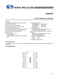
SH69P25
Block Diagram
RESET
OSCO
OSCI
OSC
WDTEN
CPU
RC
RESET
WATCHDOG
TIMER
PRESCLALER
PORTA ( 4-BITS )
PORTA [0:3]
Power
on
PORTB ( 4-BITS )
PORTB [0:3]
LPD
PORTC ( 4-BITS )
CTL REG.
PORTC [0:3]
LPDON
T0
8-BITS TIMER
( Up counter )
PORTD (4-BITS )
OTPROM
4096*16 BITS
PORTD [0:3]
PORTE ( 4-BITS )
TIMER
INTERRUPT
DATA RAM
160*4 BITS
PORTE [0:3]
PORTF ( 2-BITS )
PORTF [0:1]
Pin Description
Pin No.
Designation
I/O
Descriptions
27, 28, 1, 2
PE[0:3]
I/O
Bit programmable I/O
26, 3
PF[0:1]
I/O
Bit programmable I/O
24, 25, 4, 5
PA[0:3]
I/O
Bit programmable I/O
6
T0
I
Timer Clock/Counter input pin. (Schmitt trigger input)
7
RESET
I
Reset input (active low, Schmitt trigger input)
8
GND
P
Ground pin
9 - 12
PB[0:3]
I/O
Bit programmable I/O. Vector Interrupt (Active rising or falling edge by system
register setup)
13- 16
PD[0:3]
I/O
Bit programmable I/O
17 - 20
PC[0:3]
I/O
Bit programmable I/O. Vector Interrupt (Active rising or falling edge by system
register setup)
21
VDD
P
Power supply pin
22
OSCO
O
OSC output pin. No output for RC mode
23
OSCI
I
OSC input pin, connected to a crystal, ceramic or external resistor
2