1
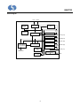
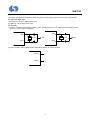
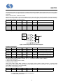
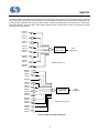
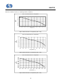
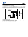
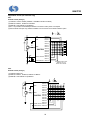
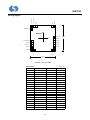
SH67P33
OTP 4-bit Micro-controller
Features
SH6610C-based single-chip 4-bit micro-controller
ROM: 1K X 16 bits OTP ROM
RAM: 48 X 4 bits RAM (Data Memory)
Operation voltage: 1.8V - 3.6V (Typical: 3.0V)
16 CMOS bi-directional I/O pins and 1 COMS input pin
4-level subroutine nesting (including interrupts)
One 8-bit auto re-loadable timer/counter
Warm-up timer for power-on reset
Powerful interrupt sources:
- Internal interrupt (Timer0).
- External interrupts: (rising edge).
PORTB & PORTC or PORTB, PORTC & PORTD (Code
Option)
Remote control programmable carrier synthesizer
Oscillator :(Code Option)
- External Ceramic Resonator/Crystal Oscillator:
400kHz - 4MHz
- Built-in RC Oscillator: 4MHz typical
Instruction cycle time:
- 4/455kHz (≈ 8.79µs) for 455kHz OSC clock
- 4/4MHz (= 1µs) for 4MHz OSC clock
Two low power operation modes: HALT and STOP
Built-in watchdog timer
OTP type/Code protection
20-pin DIP/TSSOP/SOP package
General Description
SH67P33 is dedicated to infrared remote control transmitter applications. This chip integrates the SH6610C 4-bit CPU core with
RAM, program ROM, one 8-bit timer, and programmable input/output pins and carrier synthesizer. When in standby function,
system will stop oscillator and remain low power dissipation.
Pin Configuration
1
20
VDD
PORTD.0
2
19
REM
PORTD.1
3
18
PORTA.3
PORTE.0/OSCI
4
17
PORTA.2
PORTE.1/OSCO
5
16
PORTA.1
PORTD.2
6
15
PORTA.0
PORTC.0
7
14
PORTB.3
PORTC.1
8
13
PORTB.2
PORTC.2
9
12
PORTB.1
PORTC.3
10
11
PORTB.0
SH67P33
GND
1
V2.0
SH67P33
Block Diagram
OSCI
LOW
VOLTAGE
RESET
WATCHDOG
OSCO
OSC
CPU
PORTA (4 BITS)
PRESCALER
PORTA [0:3]
PORTB (4 BITS)
PORTB [0:3]
PORTC (4 BITS)
PORTC [0:3]
PORTD (3 BITS)
8-BIT TIMER
(UP COUNTER)
CTL REG.
PORTD [0:2]
PORTE (2 BITS)
TIMER
INTERRUPT
ROM
1K X 16BIT
PORTE [0:1]
REMOTE CONTROL
SYNTHESIZER
DATA RAM
48 X 4 BIT
REM
2
SH67P33
Pin Descriptions
Pin No.
Designation
I/O
Description
7 - 10
PORTC [0:3]
I/O
2
PORTD.0
I
3, 6
PORTD [1:2]
I/O
Bit programmable I/O pins
19
REM
O
Carrier synthesizer for infrared or RF output pin
20
VDD
P
Power supply
4
PORTE.0/OSCI
I/O
Bit programmable I/O pin, shared with oscillator input pin connected to
ceramic resonator or crystal oscillator
5
PORTE.1/OSCO
I/O
Bit programmable I/O pin, shared with oscillator output pin connected to
ceramic resonator or crystal oscillator
1
GND
P
15 - 18
PORTA [0:3]
I/O
Bit programmable I/O pins
11 - 14
PORTB [0:3]
I/O
Bit programmable I/O pins, Vector Interrupt (Active rising edge)
Bit programmable I/O pins, Vector Interrupt (Active rising edge)
Input pin
Ground pin
OTP Programming Pin Description (OTP Program Mode)
Pin No.
Designation
I/O
Shared by
20
VDD
P
VDD
2
VPP
P
PORTD.0
1
GND
P
GND
4
SCK
I
PORTE.0/OSCI
15
SDA
I/O
PORTA.0
Description
Programming Power supply (+5.5V)
Programming high voltage Power supply (+11.0V)
Ground
Programming Clock input pin
Programming Data pin
3
SH67P33
Functional Description
1. CPU
The CPU contains the following functional blocks: Program
Counter (PC), Arithmetic Logic Unit (ALU), Carry Flag (CY),
Accumulator, Table Branch Register, Data Pointer (INX,
DPH, DPM, and DPL) and Stacks.
1.1. PC
The PC is used for ROM addressing consisting of 12-bits:
Page Register (PC11), and Ripple Carry Counter (PC10,
PC9, PC8, PC7, PC6, PC5, PC4, PC3, PC2, PC1, PC0).
The program counter is loaded with data corresponding to
each instruction. The unconditional jump instruction (JMP)
can be set at 1-bit page register for higher than 2K.
The program counter cans only 4K program ROM address.
(Refer to the ROM description).
1.2. ALU and CY
The ALU performs arithmetic and logic operations. The ALU
provides the following functions:
Binary addition/subtraction (ADC, SBC, ADD, SUB, ADI, SBI)
Decimal adjustments for addition/subtraction (DAA, DAS)
Logic operations (AND, EOR, OR, ANDIM, EORIM, ORIM)
Decisions (BA0, BA1, BA2, BA3, BAZ, BNZ, BC, BNC)
Logic Shift (SHR)
The Carry Flag (CY) holds the ALU overflow that the
arithmetic operation generates. During an interrupt service
or CALL instruction, the carry flag is pushed into the stack
and recovered from the stack by the RTNI instruction. It is
unaffected by the RTNW instruction.
1.3. Accumulator (AC)
The accumulator is a 4-bit register holding the results of the
arithmetic logic unit. In conjunction with the ALU, data is
transferred between the accumulator and system register, or
data memory can be performed.
1.4. Table Branch Register (TBR)
Table Data can be stored in program memory and can be
referenced by using Table Branch (TJMP) and Return
Constant (RTNW) instructions. The TBR and AC are placed
by an offset address in program ROM. TJMP instruction
branch into address ((PC11 - PC8) X (28) + (TBR, AC)). The
address is determined by RTNW to return look-up value into
(TBR, AC). ROM code bit7-bit4 is placed into TBR and
bit3-bit0 into AC.
1.5. Data Pointer
The Data Pointer can indirectly address data memory.
Pointer address is located in register DPH (3-bits), DPM
(3-bits) and DPL (4-bits). The addressing range can have
3FFH locations. Pseudo index address (INX) is used to read
or write Data memory, then RAM address bit9 - bit0 comes
from DPH, DPM and DPL.
1.6. Stack
The stack is a group of registers used to save the contents of
CY & PC (11-0) sequentially with each subroutine call or
interrupt. The MSB is saved for CY and it is organized into 13
bits X 4 levels. The stack is operated on a first-in, last-out
basis and returned sequentially to the PC with the return
instructions (RTNI/RTNW).
Note:
The stack nesting includes both subroutine calls and
interrupts requests. The maximum allowed for subroutine
calls and interrupts are 4 levels. If the number of calls and
interrupt requests exceeds 4, then the bottom of stack will be
shifted out, that program execution may enter an abnormal
state.
2. ROM
The ROM can address 1K X 16 bits of program area from $000 to $3FF.
2.1. Vector Address Area ($000 to $004)
The program is sequentially executed. There is an area address $000 through $004 that is reserved for a special interrupt
service routine such as starting vector address.
Address
Instruction
Remarks
$000
JMP instruction
Jump to RESET service routine
$001
NOP
Reserved
$002
JMP instruction
Jump to TIMER0 interrupt service routine
$003
NOP
Reserved
$004
JMP instruction
Jump to PORT interrupt service routine
* JMP instruction can be replaced by any instruction.
4
SH67P33
3. RAM
Built-in RAM contains of general-purpose data memory and system register. Because of its static nature, the RAM can keep
data after the CPU enters STOP or HALT.
3.1. RAM Addressing
Data memory and system register can be accessed in one instruction by direct addressing. The following is the memory
allocation map:
System register and I/O: $00 - $1F
Data memory: $020 - $04F
3.2. Configuration of System Register:
System Register $00-$1F RAM Map:
Address
Bit3
Bit2
Bit1
$00
$01
Bit0
R/W
-
IET0
-
IRQT0
$02
-
$03
-
Remarks
-
IEP
R/W
Interrupt enable flags
-
IRQP
R/W
Interrupt request flags
TM0.2
TM0.1
TM0.0
R/W
Timer0 Mode register (Prescaler)
-
-
-
-
Reserved
$04
TL0.3
TL0.2
TL0.1
TL0.0
R/W
Timer0 load/counter register low nibble
$05
TH0.3
TH0.2
TH0.1
TH0.0
R/W
Timer0 load/counter register high nibble
$06 - $07
-
-
-
-
-
$08
PA.3
PA.2
PA.1
PA.0
R/W
PORTA
Reserved
$09
PB.3
PB.2
PB.1
PB.0
R/W
PORTB
$0A
PC.3
PC.2
PC.1
PC.0
R/W
PORTC
$0B
-
PD.2
PD.1
PD.0
R/W
PORTD
$0C
-
-
PE.1
$0D
-
-
-
$0E
TBR.3
TBR.2
TBR.1
PE.0
REMO
REM
TBR.0
R/W
W
R
R/W
PORTE
Bit0: REMO output data
Bit0: REM pin output status
Table Branch Register
$0F
INX.3
INX.2
INX.1
INX.0
R/W
Pseudo index register
$10
DPL.3
DPL.2
DPL.1
DPL.0
R/W
Data pointer for INX low nibble
$11
-
DPM.2
DPM.1
DPM.0
R/W
Data pointer for INX middle nibble
$12
-
DPH.2
DPH.1
DPH.0
R/W
$13
PPULL
CPS2
CPS1
CPS0
R/W
$14
WDT
-
-
-
R/W
$15
LVR3
LVR2
LVR1
LVR0
R/W
$16
PACR.3
PACR.2
PACR.1
PACR.0
R/W
Data pointer for INX high nibble
Bit2-0: Carrier count source pre-divider
Bit3: Port Pull-low MOS Control
Bit3: Watchdog timer reset/flag
(Write 1 to reset WDT timer)
LVR Enable Control (LVR3 - 0):
1010: LVR Disable
Else: LVR Enable (Power-on initial 0000)
PORTA input/output control
$17
PBCR.3
PBCR.2
PBCR.1
PBCR.0
R/W
PORTB input/output control
$18
PCCR.3
PCCR.2
PCCR.1
PCCR.0
R/W
PORTC input/output control
$19
-
PDCR.2
PDCR.1
0
R/W
PORTD input/output control
$1A
-
-
PECR.1
PECR.0
R/W
PORTE input/output control
$1B
CFL3
CFL2
CFL1
CFL0
R/W
Carrier low level timer load data register (low nibble)
$1C
CFL7
CFL6
CFL5
CFL4
R/W
Carrier low level timer load data register (high nibble)
$1D
CFH3
CFH2
CFH1
CFH0
R/W
Carrier high level timer load data register (low nibble)
$1E
CFH7
CFH6
CFH5
CFH4
R/W
Carrier high level timer load data register (high nibble)
$1F
-
-
-
-
-
Reserved
5
SH67P33
4. System Clock and Oscillator
The System clock generator produces the basic clock pulses that provide the system clock with CPU and peripherals
4.1. Instruction Cycle Time:
(1) 4/455kHz (≈ 8.79µs) for 455kHz system clock.
(2) 4/4MHz (= 1µs) for 4MHz system clock
4.2. Oscillator
(1) Ceramic resonator/Crystal Oscillator: 400kHz - 4MHz. (PORTE should be set as output high before enabling pull-low
[PPULL = 1] at the program initialization.)
OSCI
OSCI
C
Ceramic
OSCO
C
Crystal
GND
C
OSCO
(2) Internal oscillator: 4MHz, PORTE.0/OSCI and PORTE.1/OSCO are used as I/O ports.
PORTE.0
PORTE.1
6
C
GND
SH67P33
5. Timer0
5.1. Configuration and Operation
Timer0 consists of an 8-bit write-only timer load register
(TL0L, TL0H), and an 8-bit read-only timer counter (TC0L,
TC0H). The counter and load register both have low order
digits and high order digits. Writing data into the timer load
register (TL0L, TL0H) can initialize the timer counter.
Load register programming: Write the low-order digit first,
and then the high-order digit. The timer counter is
automatically loaded with the contents of the load register
when the high order digit is written or counter counts
overflow from $FF to $00.
Timer Load Register: Since register H controls the physical
READ/WRITE operations, follow the following rules:
Write Operation:
Low nibble first;
High nibble to update the counter
Read Operation:
High nibble first;
Followed by Low nibble.
Load Reg. L
Load Reg. H
8-bit timer counter
Latch Reg. L
Figure 1. Timer Load register Configure
5.2. Timer0 Interrupt
The timer overflow will generate an internal interrupt request when the counter counts overflow from $FF to $00. If the interrupt
enable flag is enabled, then a timer interrupt service routine will start. This can also be used to wake CPU from HALT mode.
5.3. Timer0 Mode Register
The timer can be programmed in several different pre-scaler ratios by setting Timer Mode Register (TM0).
The 8-bit counter counts pre-scaler overflow output pulses. The TIMER mode registers (TM0) are 3-bit registers used for timer
control as shown in Table 1. These mode registers select the input pulse sources into the timer.
Table 1. Timer0 Mode Register
TM0.2
TM0.1
TM0.0
0
0
0
0
0
0
1
0
1
1
0
1
0
1
0
Pre-scaler
Divide Ratio
11
System Clock
9
System Clock
7
System Clock
5
System Clock
3
System Clock
2
System Clock
1
System Clock
0
System Clock
/2
/2
/2
/2
/2
1
0
1
/2
1
1
0
/2
1
1
1
Clock Source
/2
7
SH67P33
6. I/O PORT
The SH67P33 provides 17 I/O pins. Each I/O pin contains pull-low MOS controllable by the program. When every I/O is used as
an input port, the port control register (PCR) controls ON/OFF of the output buffer. Sections below show the circuit configuration
of I/O ports.
PORTA, PORTB, PORTC, PORTD and PORTE
Each of these ports contains 4 bit I/O pins (PORTD contains 2 bit I/O pins and 1 input pin, PORTE contains 2 bit I/O pins).
ON/OFF of the output buffer for port can be controlled by the port control register (PACR, PBCR, PCCR, PDCR and PECR).
Port I/O mapping address is shown as follows:
Address
Bit3
Bit2
Bit1
Bit0
R/W
Remarks
$08
PA.3
PA.2
PA.1
PA.0
R/W
PORTA
$09
PB.3
PB.2
PB.1
PB.0
R/W
PORTB
$0A
PC.3
PC.2
PC.1
PC.0
R/W
PORTC
$0B
-
PD.2
PD.1
PD.0
R/W
PORTD
$0C
-
-
PE.1
PE.0
R/W
PORTE
The following is the circuit configuration diagram:
PORT
CONTROL
REGISTER
PORT
DATA
REGISTER
DATA INPUT
PULL-LOW
MOS
PULL-LOW
RD_INPUT
Figure 2. Port Configuration Function Block Diagram
Port I/O Control Register:
Address
Bit3
Bit2
Bit1
Bit0
R/W
$16
PACR.3
PACR.2
PACR.1
PACR.0
R/W
PORTA input/output control
Remarks
$17
PBCR.3
PBCR.2
PBCR.1
PBCR.0
R/W
PORTB input/output control
$18
PCCR.3
PCCR.2
PCCR.1
PCCR.0
R/W
PORTC input/output control
$19
-
PDCR.2
PDCR.1
0
R/W
PORTD input/output control
$1A
-
-
PECR.1
PECR.0
R/W
PORTE input/output control
I/O control register: PACR.X, PBCR.X, PCCR.X, (X = 0, 1, 2, 3) PDCR.2, PDCR.1, PECR.1, PECR.0
1: Set I/O as an output buffer.
0: Set I/O as an input buffer (power-on initial).
Controlling the pull-low MOS
These ports contain pull-low MOS controlled by the program. PPULL register controls On/Off of all pull-low MOS
simultaneously. Pull-low MOS is controlled by the port data registers (PA, PB, PC, PD and PE) of each port also. Thus, the
pull-low MOS can be turned on and off individually.
Port Function Control (PMOD) is below:
Address
Bit 3
Bit 2
Bit 1
Bit 0
R/W
$13
PPULL
CPS2
CPS1
CPS0
R/W
PPULL:
Port Pull-low MOS enables control
0 = Disable PORT pull-low MOS (power-on initialization)
1 = Enable PORT pull-low MOS
8
Remarks
Bit3: Port Pull-low MOS Control
SH67P33
Port Interrupt
The PORTB, PORTC and PORTD can be used as port interrupt sources. Since PORT I/O is a bit programmable I/O, therefore
only the input port can generate an external interrupt. Any one of PORTB and PORTC input pins from GND to VDD will generate
an interrupt request (Default). when opt_pint is HIGH, PORTB﹑PORTC and PORTD as the port interrupt source. Thus, further
rising edge transitions can not be able to make interrupt request until all of the pins return to GND. The following is the port
interrupt function block-diagram.
PORTC.3
PCCR.3
PORTC.2
PCCR.2
PORTC.1
PCCR.1
PORTC.0
PCCR.0
RISING EDGE
DETECTION
PORTB.3
PBCR.3
PORT
INTERRUPT
PORTB.2
PBCR.2
PORTB.1
PBCR.1
Default: opt_pint = 0
PORTB.0
PBCR.0
PORTD.2
PDCR.2
PORTD.1
PDCR.1
PORTD.0
PORTC.3
PCCR.3
PORTC.2
PCCR.2
RISING EDGE
PORTC.1
PCCR.1
DETECTION
PORTC.0
PCCR.0
PORTB.3
PBCR.3
Option set: opt_pint = 1
PORTB.2
PBCR.2
PORTB.1
PBCR.1
PORTB.0
PBCR.0
Figure 3. PORT Interrupt Block Diagram
9
PORT
INTERRUPT
SH67P33
7. Remote Control Synthesizer
SH67P33 has a carrier synthesizer for infrared or RF remote control circuits.
Address
Bit3
Bit2
Bit1
Bit0
R/W
$0D
-
-
-
REMO
REM
W
R
$13
PPULL
CPS2
CPS1
CPS0
R/W
Remarks
Bit0: REMO output data
Bit0: REM pin output status
Bit2 - 0: Carrier count source pre-divider
Bit3: Port Pull-low MOS Control
REMO: Remote output data control. The REM pin output status can be ready by instruction.
CPS2 - 0: Carrier counter source pre-divider control Register
The carrier synthesizer can be programmed in several different pre-scaler ratios by setting CPS2 - 0.
Carrier source pre-divider control Register
CPS2
CPS1
CPS0
0
0
0
0
0
0
System clock/2
1
1
0
Pre-scaler
Divide Ratio
11
System Clock
9
System Clock
7
System Clock
5
System Clock
3
System Clock
2
System Clock
1
System Clock
0
System Clock
System clock /2
0
1
Clock Source
System clock /2
1
System clock /2
1
0
0
System clock /2
1
0
1
System clock /2
1
1
1
0
1
System clock /2
1
System clock /2
The carrier-generating counter is an 8-bit count-up counter and it has two-reload data register. The counter and load registers
both have low order digits and high order digits. Writing data into the timer load registers ($1B, $1C, $1D, $1E) can initialize the
counter.
After system reset, the counter is automatically loaded with the contents of high level timer load data register ($1E, $1D) and
output high level at the same time. Following when counter counts overflow from $FF to $00, the counter is automatically
loaded with the contents of low level timer load data register ($1C, $1B) and output low level at the same time. When counter
counts overflow again from $FF to $00 again, the counter will be loaded with the contents of high level timer load data register
again. The above sequences make up a complete loop. So the carrier synthesizer can output continuous carrier wave of certain
duty and certain period.
Load register programming: User can modify low level timer load data register ($1B, $1C) to change the width of the low level.
User can also modify high level timer load data register ($1D, $1E) to change the width of high level. In the way the carrier
synthesizer can output carrier wave of different duty and different period.
Carrier load data register
Address
Bit3
Bit2
Bit1
Bit0
R/W
Remarks
$1B
CFL3
CFL2
CFL1
CFL0
R/W
Carrier low level timer load data register (low nibble)
$1C
CFL7
CFL6
CFL5
CFL4
R/W
Carrier low level timer load data register (high nibble)
$1D
CFH3
CFH2
CFH1
CFH0
R/W
Carrier high level timer load data register (low nibble)
$1E
CFH7
CFH6
CFH5
CFH4
R/W
Carrier high level timer load data register (high nibble)
10
SH67P33
C
P
S
2
SYSTEM
CLOCK
C
P
S
1
C
P
S
0
Low level timer load data
register
Prescaler
divider
Carrier
output
Carrier generating
counter
High level timer load data
register
REM
REMO
CARRIER SYNTHESIZER
Figure 4. Remote Control Functional Block Diagram
COUNTER
SOURCE
RESET
SIGNAL
REMO
COUNTER
OVERFLOW
2 3
1
1:load high level data register
2
3
2
2
1
3
2
2:High level counter overflow and load lowlevel data register
3:Low level counter overflow and load high level data register
MODIFY
HIGH&LOW
DATA
REGISTER
CARRIER
OUTPUT
OUTPUT
OUTPUT
HIGH
HIGH
LEVEL OUTPUT LEVEL OUTPUT
LOW
LOW
LEVEL
LEVEL
(255n1)clock
interval
(255n2)clock
interval
carrier wave
period
n1Dec=($1E,$1D)Hex
n2Dec=($1C,$1B)Hex
REM
Figure 5. Carrier Synthesize Wave
11
3
2
3
SH67P33
8. Interrupt
Two interrupt sources are available on SH67P33 :
- Timer0 overflow interrupt
- Port's rising edge detection interrupt (PBC)
Interrupt Control Bits and Interrupt Service
The interrupt control flags are mapped on $00 through $01 of the system register. They can be accessed or tested by the
program. These flags are cleared to 0 at initialization by chip reset.
Address
Bit3
Bit2
Bit1
Bit0
Remarks
$00
-
IET0
-
IEP
Interrupt enable flags
$01
-
IRQT0
-
IRQP
Interrupt request flags
When IEx is set to 1 and the interrupt request is generated (IRQx is 1), the interrupt will be activated and vector address will be
generated from the priority PLA corresponding to the interrupt sources. When an interrupt occurs, the PC and CY flag will be
saved into stack memory and jump to interrupt service vector address. After the interrupt occurs, all interrupt enable flags (IEx)
are reset to 0 automatically, thus, when IRQx is 1 and IEx is set to 1 again, the interrupt will be activated and vector address will
be generated from the priority PLA corresponding to the interrupt sources.
Interrupt Servicing Sequence Diagram:
1
2
3
Instruction
Execution
N
Instruction
Execution
I1
Instruction
Execution
I2
Interrupt Generated
Interrupt Accepted
4
5
Inst. cycle
Vector Generated
Stacking
Fetch Vector address
Reset IE.X
Start at vector
address
Interrupt Nesting:
During the SH6610C CPU interrupt service, the user can enable any interrupt enable flag before returning from the interrupt.
The servicing sequence diagram shows the next interrupt and the next nesting interrupt occurrences. If the interrupt request is
ready and the instruction of execution N is IE enable, then the interrupt will start immediately after the next two instruction
executions. However, if instruction I1 or instruction I2 disables the interrupt request or enable flag, then the interrupt service will
be terminated.
9. HALT and STOP Mode
After the execution of HALT instruction, SH67P33 will enter HALT mode. In HALT mode, the CPU will stop operating; however,
the peripheral circuit (timer) will keep operating.
After the execution of STOP instruction, SH67P33 will enter STOP mode.
In STOP mode, the entire chip (including oscillator) will stop operating.
In HALT mode, SH67P33 can be woken up if an interrupt occurs.
In STOP mode, SH67P33 can be woken up if a port interrupt occurs.
10. Warm-up Timer
The SH67P33 has a built-in oscillator warm-up timer to eliminate unstable state of initial oscillation when oscillator starts
oscillating in the following conditions:
- Power-on reset
- Wake-up from STOP mode
- Low voltage reset
The warm-up counter pre-scaler is divided by 213 (8192).
(1) When SH67P33 operates in 455kHz frequency, the warm-up time interval is about 18 ms.
(2) When SH67P33 operates in 4MHz frequency, the warm-up time interval is about 2 ms.
12
SH67P33
11. Low Voltage Reset (LVR)
The LVR function monitors the supply voltage and applies an internal reset in the micro-controller at battery replacement. If the
applied circuit satisfies the following conditions, the LVR can be incorporated by the software control.
The LVR circuit has the following functions:
Generates an internal reset signal when VDD ≤ VLVR (typ: 1.5V).
System Register $15
Address
Bit3
Bit2
Bit1
Bit0
R/W
$15
LVR3
LVR2
LVR1
LVR0
R/W
Remarks
LVR Enable Control (LVR3 - 0): 1010: LVR Disable
Else: LVR Enable (Power-on initial 0000)
12. Watchdog Timer
Watchdog timer is a 16-bit down-count counter, and its clock source is internal RC oscillator. The watchdog timer automatically
generates a device reset when it overflows. To prevent it timing out and generating a device RESET condition, users should
write bit3 of system register $14 as “1” before timing-out. The WDT has a time-out period of approx. 16ms. WDT bit3 is
watchdog timer overflow flag.
System Register $14 (WDT)
Address
Bit 3
Bit 2
Bit 1
Bit 0
$14
WDT
-
-
-
R/W
Remarks
R/W Bit3: Watchdog timer reset/flag (Write 1 to reset WDT timer)
The WDT bit is cleared only if the Watchdog Timer time-out occurred both in normal operation mode and in the HALT mode.
The Watchdog Timer is cleared when the device wakes up from the STOP mode, regardless of the source of wake-up.
13. Reset Function
The SH67P33 has the power-on reset circuit, though it does not have RESET pin. System reset is performed automatically at
power-on, and software starts program from address $000.
In order to make the built-in power-on reset circuit operate efficiently, set the voltage rising time until VDD = 0V to 2.2V is
obtained at power-on 1ms or less.
VDD
Power-on reset
circuit output voltage
Reset state
Internal reset
signal
Reset released
Power-on
13
SH67P33
14. Initial State
There are 3 types of system resets:
1. Power-on reset
2. Low Voltage Reset
3. Watchdog reset
Hardware
After power-on reset
After LVR reset
After WDT reset
$000
$000
$000
CY
Undefined
Unchanged
Unchanged
Data memory
Undefined
Unchanged
Unchanged
System register
Undefined
Unchanged
Unchanged
AC
Undefined
Unchanged
Unchanged
Timer counter
0
Unchanged
Unchanged
Timer load register
0
Unchanged
Unchanged
LVR
0000
0000
Unchanged
I/O ports
Input
Input
Input
0
Unchanged
Unchanged
CPS2 - 0
Undefined
Unchanged
Unchanged
Carrier low level timer load data register
Undefined
Unchanged
Unchanged
WDT
1
1
0
REMO
0
0
0
Program counter
PPULL
15. Code Option
15.1. Oscillator Select
0 = 4MHz built-in RC oscillator (default)
1 = External Ceramic resonator/Crystal Oscillator: 400kHz - 4MHz (PORTE should be set as output high before enabling
pull-low [PPULL = 1] at the program initialization.)
15.2. Port Interrupt Source Select
0 = PORTB, PORTC interrupt (default)
1 = PORTB, PORTC, PORTD interrupt
14
SH67P33
Instruction Set
All instructions are one cycle and one-word instructions. The characteristics are memory-oriented operation.
Arithmetic and Logical Instructions
Accumulator Type
Mnemonic
Instruction Code
Function
Flag Change
ADC
X (, B)
00000 0bbb xxx xxxx
AC
← Mx + AC + CY
CY
ADCM
X (, B)
00000 1bbb xxx xxxx
AC, Mx ← Mx + AC + CY
CY
ADD
X (, B)
00001 0bbb xxx xxxx
AC
← Mx + AC
CY
ADDM
X (, B)
00001 1bbb xxx xxxx
AC, Mx ← Mx + AC
CY
SBC
X (, B)
00010 0bbb xxx xxxx
AC
← Mx + -AC + CY
CY
SBCM
X (, B)
00010 1bbb xxx xxxx
AC, Mx ← Mx + -AC + CY
CY
SUB
X (, B)
00011 0bbb xxx xxxx
AC
← Mx + -AC + 1
CY
CY
SUBM
X (, B)
00011 1bbb xxx xxxx
AC, Mx ← Mx + -AC + 1
EOR
X (, B)
00100 0bbb xxx xxxx
AC
EORM
X (, B)
00100 1bbb xxx xxxx
AC, Mx ← Mx ⊕ AC
OR
X (, B)
00101 0bbb xxx xxxx
AC
ORM
X (, B)
00101 1bbb xxx xxxx
AC, Mx ← Mx | AC
AND
X (, B)
00110 0bbb xxx xxxx
AC
ANDM
X (, B)
00110 1bbb xxx xxxx
AC, Mx ← Mx & AC
0 → AC [3]; AC [0] →CY;
AC shift right one bit
SHR
11110 0000 000 0000
← Mx ⊕ AC
← Mx | AC
← Mx & AC
CY
Immediate Type
Mnemonic
Instruction Code
Function
Flag Change
ADI
X, I
01000 iiii xxx xxxx
AC
← Mx + I
CY
ADIM
X, I
01001 iiii xxx xxxx
AC, Mx ← Mx + I
CY
SBI
X, I
01010 iiii xxx xxxx
AC
← Mx + -I +1
SBIM
X, I
01011 iiii xxx xxxx
AC, Mx ← Mx + -I + 1
EORIM
X, I
01100 iiii xxx xxxx
AC, Mx ← Mx ⊕ I
ORIM
X, I
01101 iiii xxx xxxx
AC, Mx ← Mx I I
ANDIM
X, I
01110 iiii xxx xxxx
AC, Mx ← Mx & I
CY
CY
Decimal Adjust
Mnemonic
Instruction Code
Function
Flag Change
DAA X
11001 0110 xxx xxxx
AC; Mx ← Decimal adjust for add.
CY
DAS X
11001 1010 xxx xxxx
AC; Mx ← Decimal adjust for sub.
CY
Function
Flag Change
Transfer Instruction
Mnemonic
Instruction Code
LDA
X (, B)
00111 0bbb xxx xxxx
AC
← Mx
STA
X (, B)
00111 1bbb xxx xxxx
Mx
← AC
X, I
01111 iiii xxx xxxx
LDI
AC, Mx ← I
15
SH67P33
Control Instruction
Mnemonic
Instruction Code
Function
Flag Change
BAZ X
10010 xxxx xxx xxxx
PC
← X if AC = 0
BNZ X
10000 xxxx xxx xxxx
PC
← X if AC ≠ 0
BC
X
10011 xxxx xxx xxxx
PC
← X if CY = 1
BNC X
10001 xxxx xxx xxxx
PC
← X if CY ≠ 1
BA0 X
10100 xxxx xxx xxxx
PC
← X if AC (0) = 1
BA1 X
10101 xxxx xxx xxxx
PC
← X if AC (1) = 1
BA2 X
10110 xxxx xxx xxxx
PC
← X if AC (2) = 1
BA3 X
10111 xxxx xxx xxxx
PC
← X if AC (3) = 1
CALL X
11000 xxxx xxx xxxx
ST
PC
← CY; PC + 1
← X (Not include p)
11010 000h hhh llll
PC
AC
←ST; TBR ← hhhh;
←llll
RTNI
11010 1000 000 0000
CY; PC ← ST
HALT
11011 0000 000 0000
STOP
11011 1000 000 0000
JMP X
1110p xxxx xxx xxxx
PC ← X (Include p)
TJMP
11110 1111 111 1111
PC ← (PC11 - PC8) (TBR) (AC)
NOP
11111 1111 111 1111
No Operation
RTNW H; L
CY
Where,
PC
Program counter
I
Immediate data
AC
Accumulator
⊕
Logical exclusive OR
-AC
Complement of accumulator
|
Logical OR
CY
Carry flag
&
Logical AND
Mx
Data memory
P
ROM page = 0
ST
Stack
16
bbb
RAM bank = 000
TBR
Table Branch Register
SH67P33
Electrical Characteristics
Absolute Maximum Ratings*
*Comments
DC Supply Voltage . . . . . . . . . . . . . . .-0.3V to +6.0V
Stresses above those listed under "Absolute Maximum
Ratings" may cause permanent damage to this device.
These are stress ratings only. Functional operation of this
device under these or any other conditions above those
indicated in the operational sections of this specification is
not implied or intended. Exposure to the absolute maximum
rating conditions for extended periods may affect device
reliability.
Input Voltage . . . . . . . . . . . . . . . -0.3V to VDD + 0.3V
Operating Ambient Temperature . . . . -10℃ to +70℃
Storage Temperature . . . . . . . . . . . . -55℃to +125℃
DC Electrical Characteristics (VDD = 3.0V, GND = 0V, TA = -10 to 70℃, fOSC = 4MHz, unless otherwise specified)
Symbol
VDD
VRAM
Parameter
Min.
Typ.
Max.
Unit
Operating Voltage
1.8
3.0
3.6
V
RAM Retention Voltage
1.1
-
3.6
V
Condition
IOP
Operating Current
-
0.3
1
mA
All output pins unload
(Execute NOP instruction)
ISB1
HALT Current
-
200
-
µA
CPU in HALT mode; ALL output pins unload
ISB2
STOP Current
-
-
1
µA
OSC STOP
ALL output pins unload, LVR on
IREML
REM sink current
0.3
-
-
mA
VREM = 0.3V
IREMH
REM driving current
-5
-9
-
mA
VREM = 1V
VIL
Input Low Voltage
GND
-
VDD X 0.2
V
I/O ports, Schmitt Trigger input
VIH
Input High Voltage
VDD X 0.8
-
VDD
V
I/O ports, Schmitt Trigger input
IIL
Input Leakage Current
-0.2
-
0.2
µA
I/O ports; VI/O = VDD or GND
IIH
High-level Input Current
-30
-
-10
µA
I/O ports with pull-low; VI/O = VDD (excluding
PORTD.0)
IIH1
High-level Input Current
-30
-
-6
µA
PORTD.0 input with pull-low; VI/O = VDD
VOH
Output High Voltage
VDD - 0.7
-
-
V
I/O ports, IOH = -1mA
VOL
Output Low Voltage
-
-
GND + 0.6
V
I/O ports, IOL = 5mA
-
-
1
ms
Min.
Typ.
Max.
Unit
1.2
1.5
1.8
V
TPON
Power-on reset circuit valid
power source rising time
VDD = 0 to 2.2 V
LVR Circuitry (TA = −10℃ to +70℃)
Symbol
VLVR
Parameter
LVR Voltage
Condition
LVR Enable
AC Electrical Characteristics (VDD = 3.0V, GND = 0V, TA = 25℃, built-in RC oscillator, unless otherwise specified)
Symbol
Parameter
Min.
Typ.
Max.
Unit
Conditions
tOSC
Oscillator Start time
-
-
20
ms
fOSC1
Frequency Variation
3.92
4
4.08
MHz
VDD = 2.0 to 3.6V, TA = +5℃ to +45℃
fOSC2
Frequency Variation
3.88
4
4.12
MHz
VDD = 2.0 to 3.6V, TA = -10℃ to +45℃
fOSC3
Frequency Variation
3.80
-
4.00
MHz
VDD = 2.0 to 3.6V, TA = +45℃ to +70℃
17
Ceramic Resonator = 455kHz
SH67P33
RC Oscillator Characteristics Graphs (for reference only)
Built-in RC oscillator Frequency vs. Operating Ambient Temperature:
VDD = 3.0V, Built-in RC fosc vs. Temperature
4.09
4.07
4.05
fosc
(MHz)
4.03
4.01
3.99
3.97
3.95
3.93
-45
-30
-15
0
15
30
45
60
75
90
Temperature (℃)
Graph 1 Built-in RC fOSC vs. Temperature (VDD = 3.0V)
VDD = 2.0V, Built-in RC fosc vs. Temperature
4.03
4.01
fosc
(MHz)
3.99
3.97
3.95
3.93
3.91
3.89
-45
-30
-15
0
15
30
45
60
75
90
75
90
Temperature (℃)
Graph 2 Built-in RC fOSC vs. Temperature (VDD = 2.0V)
fOSC
(MHz)
VDD = 3.6V, Built-in RC fosc vs. Temperature
4.10
4.08
4.06
4.04
4.02
4.00
3.98
3.96
3.94
3.92
-45
-30
-15
0
15
30
45
60
Temperature (℃)
Graph 3 Built-in RC fOSC vs. Temperature (VDD = 3.6V)
18
SH67P33
In System Programming Notice for OTP
The In System Programming technology is valid for OTP chip.
The Programming Interface of the OTP chip must be set on the user’s application PCB, and users can assemble all
components including the OTP chip in the application PCB before programming the OTP chip. Of course, it’s accessible
bonding OTP chip only first, and then programming code and finally assembling other components.
Since the programming timing of Programming Interface is very sensitive, therefore four jumpers are needed (VDD, VPP, SDA,
SCK) to separate the programming pins from the application circuit as shown in the following diagram.
Application PCB
OTP Chip
VPP
VDD
SCK
OTP Writer
SDA
GND
To Application
Circuit
Jumper
The recommended steps are as following:
(1) The jumpers are open to separate the programming pins from the application circuit before programming the chip.
(2) Connect the programming interface with OTP writer and begin programming.
(3) Disconnect OTP writer and short these jumpers when programming is complete.
For more detail information, please refer to the OTP writer user manual.
19
SH67P33
Application Circuit (for reference only)
AP1:
Remote Control (48 Keys)
(1) Oscillator: Ceramic 455kHz (PORTE0, 1 SHARED TO OSCI & OSCO)
(2) PORTA, PORTD.1, PORTD.2: I/O Buffers
(3) PORTB, C and PORTD.0: Input Buffers
(4) R1 = 0 is possible, but the REM specification is revised to reduce power consumption
(5) Since PORTD.0 is input only, PORTB or PORTC can be scanned out to detect PORTD.0 option.
R1
100P
VDD
PORTD.2
PORTD.1
GND
PORTD.0
PORTC.3
PORTC.2
PORTC.1
REM
PORTC.0
SH67P33 PORTB.3
PORTB.2
PORTB.1
PORTB.0
PORTA.3
PORTE.1/OSCO PORTA.2
PORTA.1
PORTE.0/OSC1 PORTA.0
Simplified Custom Code
Selection only one
switch can be closed
100P
AP2:
Remote Control (81 Keys)
(1) Oscillator: Built-in RC
(2) PORTA, PORTD.1, PORTD.2, PORTE: I/O Buffers
(3) PORTB, C and PORTD.0: Input Buffers
VDD
GND
R1
PORTD.2
PORTD.1
PORTD.0
PORTC.3
PORTC.2
PORTC.1
REM
PORTC.0
PORTB.3
SH67P33 PORTB.2
PORTB.1
PORTB.0
PORTA.3
PORTA.2
PORTE.1/OSCO
PORTA.1
PORTE.0/OSCI PORTA.0
20
VDD
SH67P33
Bonding Diagram
PORTE.0/OSCI
P
O
R
T
D
.
1
P
O
R
T
D
.
0
G
N
D
3
2
1
V
D
D
R
E
M
20 19
4
Y
SH67P33
18
PORTA.3
17
PORTA.2
5
16
PORTA.1
6
15
PORTA.0
X
(0,0)
PORTE.1/OSCO
PORTD.2
7
14
PORTB.3
PORTC.1
8
13
PORTB.2
PORTC.2
9
PORTC.0
10
11 12
P
O
R
T
C
.
3
P
O
R
T
B
.
0
1630µm
1570µm
P
O
R
T
B
.
1
Substrate connects to GND.
unit: µm
Pad Location
Pad NO.
1
2
3
4
5
6
7
8
9
10
11
12
13
14
15
16
17
18
19
20
Designation
GND
PORTD.0
PORTD.1
PORTE.0/OSCI
PORTE.1/OSCO
PORTD.2
PORTC.0
PORTC.1
PORTC.2
PORTC.3
PORTB.0
PORTB.1
PORTB.2
PORTB.3
PORTA.0
PORTA.1
PORTA.2
PORTA.3
REM
VDD
21
X
-484.00
-602.00
-722.00
-733.00
-728.00
-745.00
-745.00
-745.00
-734.00
-614.00
614.00
734.00
745.00
745.00
745.00
745.00
745.00
745.00
733.00
618.00
Y
712.50
712.50
712.50
562.05
-180.65
-322.50
-437.50
-552.50
-707.50
-707.50
-707.50
-707.50
-552.50
-432.50
-312.50
-192.50
-72.50
67.50
700.50
700.50
SH67P33
Ordering Information
Part No.
Package
SH67P33H
Chip Form
SH67P33X
20L TSSOP
SH67P33
20L DIP
SH67P33M
20L SOP
22
SH67P33
Package Information
unit: inches/mm
TSSOP 20L Outline Dimensions
Symbol
A
A1
A2
A3
bp
c
D(1)
E(2)
e
HE
L
Lp
Q
v
w
y
Z(1)
θ
Dimensions in mm
Dimensions in inch
MIN
NOM
MAX
MIN
NOM
MAX
--0.05
0.80
--0.19
0.1
6.4
4.3
--6.2
--0.5
0.3
------0.2
0°
------0.25
--------0.65
--1
----0.2
0.13
0.1
-----
1.1
0.15
0.95
--0.30
0.2
6.6
4.5
--6.6
--0.75
0.4
------0.5
8°
--0.002
0.032
--0.008
0.004
0.256
0.172
--0.248
--0.02
0.012
------0.008
0°
------0.01
--------0.026
--0.04
----0.008
0.005
0.004
-----
0.044
0.006
0.038
--0.012
0.008
0.264
0.18
--0.264
--0.03
0.016
------0.02
8°
Notes:
1. Plastic or metal protrusions of 0.15 mm maximum per side are not included.
2. Plastic interlaid protrusions of 0.25 mm maximum per side are not included.
23
SH67P33
DIP 20L Outline Dimensions
unit: inches/mm
D
11
E1
20
1
10
E
A1
A2
Base Plane
Seating Plane
L
A
C
S
B
e1
B1
a
Symbol
Dimensions in inches
Dimensions in mm
A
0.175 Max.
4.45 Max.
A1
0.010 Min.
0.25 Min.
A2
0.130 ± 0.010
3.30 ± 0.25
B
0.018 +0.004
-0.002
0.46 +0.10
-0.05
B1
0.060 +0.004
-0.002
1.52 +0.10
-0.05
C
0.010 +0.004
-0.002
0.25 +0.10
-0.05
D
1.026 Typ. (1.046 Max.)
26.06 Typ. (26.57 Max.)
E
0.300 ± 0.010
7.62 ± 0.25
E1
0.250 Typ. (0.262 Max.)
6.35 Typ. (6.65 Max.)
e1
0.100 ± 0.010
2.54 ± 0.25
L
0.130 ± 0.010
3.30 ± 0.25
α
0° ~ 15°
0° ~ 15°
eA
0.345 ± 0.035
8.76 ± 0.89
S
0.078 Max.
1.98 Max.
Notes:
1. The maximum value of dimension D includes end flash.
2. Dimension E1 does not include resin fins.
3. Dimension S includes end flash.
24
eA
SH67P33
SOP 20L (W.B.) Outline Dimensions
unit: inches/mm
20
11
e1
HE
E
~
~
θ
L
1
10
Detail F
e1
e
Seating Plane
D
S
b
A
LE
A1
A2
c
D
y
See Detail F
Symbol
Dimensions in inches
Dimensions in mm
A
0.106 Max.
2.69 Max.
A1
0.004 Min.
0.10 Min.
A2
0.092 ± 0.005
2.33 ± 0.13
b
0.016 +0.004
-0.002
0.41 +0.10
-0.05
C
0.010 +0.004
-0.002
0.25 +0.10
-0.05
D
0.500 ± 0.02
12.80 ± 0.51
E
0.295 ± 0.010
7.49 ± 0.25
e
0.050 ± 0.006
1.27 ± 0.15
e1
0.376 NOM.
9.50 NOM.
HE
0.406 ± 0.012
10.31 ± 0.31
L
0.032 ± 0.008
0.81 ± 0.20
LE
0.055 ± 0.008
1.40 ± 0.20
S
0.042 Max.
1.07 Max.
y
0.004 Max.
0.10 Max.
θ
0° ~ 10°
0° ~ 10°
Notes:
1. The maximum value of dimension D includes end flash.
2. Dimension E does not include resin fins.
3. Dimension e1 is for PC Board surface mount pad pitch. Designer reference only.
4. Dimension S includes end flash.
25
SH67P33
Data Sheet Revision History
Version
Content
Date
2.0
1. Add Reset Function Description (Page 13)
2. Add “Power-on reset circuit valid power source rising time” specification (Page 17)
3. Simplify Ordering Information (Page 22)
2005.2
1.0
Original
2004.9
26