1
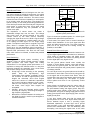
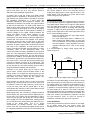
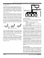
App Note 202
Design Considerations in Mixed Signal
System Boards
This application note is for use in conjunction with Anadigm software which is subject to the terms of an Anadigm software license.
This application note does not form part of any contract or specification between Anadigm and the user and is for guidance and
illustration only. Accordingly, we accept no liability arising out of the use of the guidance note in conjunction with the software to the
extent permitted by law.
Introduction
Designing a mixed signal system board, requires careful
considerations related to routing signals, system
partitioning and handling circuit grounds and power
signals.
This Application Note discusses some of these
®
considerations to help you design Anadigm FPAA
devices in such systems while achieving maximum
performance. The following topics are covered in this
Application Note:
• FPAA technology background
• Grounding and ground planes
• Power planes, power decoupling and power
distribution in mixed signal systems
• Analog and digital signal paths
• Clock distribution
• Component selection
FPAA technology background
Anadigm®'s field programmable analog arrays (FPAAs)
and design software introduce two new capabilities to the
analog world. The first is the ability to translate complex
analog circuits to a simple set of low-level functions, and
thus to give designers the analog equivalent of an FPGA.
The second is the ability to place analog functions under
real-time software control within the system.
By providing the analog equivalent of logic gates, FPAAs
give designers the ability to describe analog functions
such as gain stages and filters without reference to the
underlying function - in other words, without having to
think on the level of such components as op amps,
capacitors, resistors, transconductors, and current
mirrors. Lifted to this higher level of abstraction, the
design process becomes so simple that non-specialists
can create sophisticated circuits that would require
weeks or months of design work with ASICs or discretes.
Dynamic reconfigurability adds to these capabilities by
allowing analog functions to be updated in real time
using automatically generated C-code. With analog
functions under the control of the system processor, new
device configurations can be loaded on the fly, allowing
the device's operation to be "time-sliced," or to
manipulate the tuning or the construction of any part of
Anadigm
®
the circuit without interrupting operation of the FPAA,
thus maintaining system integrity.
®
To get more information on the Anadigm FPAA
technology and our solutions, please visit our website at
http://www.anadigm.com.
Grounding and ground planes
System Ground
In a mixed signal system there are several different types
of ‘ground’. One of them is the ‘system ground’, which all
boards and modules in the system share. The most
common problem within such systems is the ‘common
ground impedance’ – illustrated in Figure 1.
Circuit 1
Ground
Current
1
Circuit 2
Common
Ground
Impedence
Ground
Current
2
Figure 1: Common Ground Impedance
The figure shows how current flowing from circuit 1 to
ground can potentially produce noise in Circuit 2, by
modulating its ground potential. Such common ground
impedances are created by ‘daisy chain grounding’.
Instead ‘star grounding’ (shown in Figure 2) is
recommended. Additionally all ground connections need
to be made with large diameter wires or wide PCB
traces.
Daisy Chain
Star Ground
Figure 2: Daisy Chain vs. Star Ground
AP020800-U202
®
Copyright © 2002 Anadigm , All Rights Reserved
A pp Note 202 —Design Considerations in Mixed Signal System Boards
Board Ground Traces
Of most interest to board level designers are the common return currents of individual components. Any signal
running on a PCB trace creates a return current, which
flows through the ground connection. This return current
follows the route of minimum impedance; it would prefer
to run directly under the signal trace. Thus single layer
boards normally do not show good analog performance.
Even dual layer boards need careful layout of signal and
return paths, to make them clean. Since wider traces
have lower impedance, they are preferable for the
current return path.
The impedance of narrow traces can create a
measurable voltage drop over the trace. This voltage
drop would move the ground potential of the return
currents source by the same amount, effectively
changing the signal at the source. While a signal change
of 5mV may be acceptable in a digital system, it is 0.1%
of an analog full scale signal in a 5V single supply
system. The optimum return path for a signal is a ground
plane, where a complete layer is filled with copper,
serving as a very low impedance ground connection. A
ground plane, because of its low impedance, also greatly
improves EMI performance. But there are still some
rules, which have to be followed, to obtain best possible
performance.
Board Partitioning
Consider a mixed signal system consisting of an
®
Anadigm FPAA, an analog to digital converter, a digital
signal processor and other digital and analog
components. For the highest system performance, it is
important to arrange the different blocks in a way that
interac tion between the potentially noisy circuit blocks
and sensitive analog circuits is minimized.
• Group logic circuits according to the operating
speed.
Keep
all
high-frequency
logic
components close together, preferably close to
the connector so that all high-frequency trace
lengths are minimized. Short trace lengths
reduce the amount of distributed capacitance
and mutual inductance between signal routes.
Place the low-frequency logic further away on
the board, since longer trace lengths are
acceptable.
• Similarly, group and separate analog circuits
according to frequency, minimizing the length of
high-frequency signal paths.
• Minimize the interface between the analog and
the digital circuits by careful layout designed to
minimize interaction.
Anadigm
®
Analog
Circuits
Logic
Circuits
Analog
Interface
Logic
Interface
Connector
Analog
Analog System
Interface Circuits Clock
Connector
High
Frequency
Digital
Low
Frequency
Digital
Figure 3: Two ways of laying out a mixed signal board for
highest system performance.
Figure 3 shows two possible layouts of a mixed signal
system board optimized for performance.
In both cases, the system clock is located centrally to
enable direct distribution of the clock signal with short
traces and without through-holes. The higher frequency
parts are as far away from the analog circuitry as
possible, to avoid EMI.
Ground Plane Rules and Layout
A good way to ensure that the interaction between analog and digital signals will be minimized is to isolate the
circuit areas on separate analog and digital ground
planes. An analog plane will contain only analog circuits
and the digital plane only digital circuits.
The two ground planes should never overlap one
another. If ground planes overlap, current will perfectly
couple from one ground plane into the other. A multilayer board with power and ground planes is optimal, but
not always practical.
On a two layer board, the ground plane area should be
maximized on both sides of the board by using trace fill
on the signal side of the printed circuit board. Trace fill
involves filling the open area between signal traces with
copper and connecting this "mini-plane" to ground.
Ground planes and trace fill can significantly reduce
coupling.
Power planes are designed using the same rules as
ground planes. If power planes are used, never bridge
the split between analog and digital ground. Keep the
analog supply plane entirely under (over) the analog
ground plane. This gives an analog supply plane over the
analog ground plane and a digital supply plane over the
digital ground plane.
In four layer boards make sure that the power and
ground planes are on the inner layers. Most PCB’s are
thinner between layers 2 and 3, providing higher
distributed capacitance. A power layer over a ground
layer provides a very good decoupling capacitor, with
almost ideal characteristics. This can drastically ease
decoupling. Also having the signal trace on the outer
AP020800-U202
Copyright © 2002 Anadigm®. All Rights Reserved
A pp Note 202 —Design Considerations in Mixed Signal System Boards
layers of the board is beneficial, as the inner layers with
ground and power act as a very efficient shield to
attenuate coupling between signal traces.
A general rule is that the analog and digital ground
planes should be separated by at least 3mm (I/8"). The
gap between the ground planes is intended to minimize
the distributed capacitance to a point where the
interaction between the ground planes is minimal. This
capacitance is based on the length of the ground plane
as well as the separation. On small boards where the
distance of the ground plane split is small, the gap width
can be reduced. At some place in the circuit, the analog
and digital grounds must be tied together to establish a
common voltage for the digital interface between the
analog and digital circuits. Proper selection of this
connection point is crucial to maximizing system
performance. One must attempt to keep the digital return
currents that flow back to the regulator from passing
through the analog circuits, and vice-versa. In this case
the centralized location of the power supply regulation is
beneficial; all power supply return currents have a direct
path back to the regulators. In most layouts the best
point to tie analog and digital grounds together is never
completely clear. At the prototyping stage, pick
numerous locations as likely candidates for the ground
plane tie. Then experiment to determine which location
maximizes analog performance, and use that point as
the ground tie. Ideally a sec ond pass layout of the board
will allow the ground tie to be permanently etched into
the circuit board. A nice wide ground tie provides good
connection between grounds at all frequencies. The
inductance of a thin wire jumper will limit its effectiveness
at high frequencies, and could pos sibly cause a shift in
the ground potential between the two planes.
Trenches in the ground plane can be used to direct
ground return currents around sensitive areas of the
analog section. For example the high-frequency ground
currents of the audio converters and the FPAA can be
kept away from areas, where the low voltage, lowfrequency signals are routed on the board.
Such fractures can also be used, to control current flow
between high current and low current circuit areas, and
to isolate the noise from high frequency clocks. But do
not put too many cuts into the ground plane, as they
would disrupt the continuity of the current flows and limit
the effectiveness of the ground plane.
Mixed signal parts, like converters or FPAA’s should be
placed close to the ground split, with the digital pins fac ing the split. In the past it was recommended, to place
such IC’s over the split, with analog pin over the analog
plane, digital pins over the digital plane, analog ground
pins connected to the analog plane and digital pins connected to the digital plane. This is no longer
recommended, for several reasons. One important
reason is the fact, that analog and digital ground cannot
be completely separated on the die. So it is possible, that
Anadigm
®
“analog” return currents flow out of the “digital” pin. Now
this current needs to flow to the connection point of
analog and digital ground, which might be down in the
power supply. This can take a long time, which would
create timing and noise problems.
Power Considerations
For performance reasons it is always highly recommend
to use separate supplies for digital and analog circuitry.
The digital supply should only be used for parts placed
over the digital ground plane, i.e. all pure digital parts.
The analog supply is used for all analog and mixed signal parts. It might look like a good idea, to use the digital
supply for the digital pins of the mixed signal parts, but it
is not, for the following reasons:
Doing this would bring the noisy digital supply
into the analog region.
For most mixed signal parts a difference between analog and digital supply of more than
0.5V is not allowed. This can easily be exceeded
with dual supplies, if both regulators are at the
opposite tolerances and if noise on the supply
adds up.
It is recommended, to supply mixed signal parts as
shown in Figure 4.
10 Ohm
or Ferrite Bead
Analog
Supply
Digital
Supply
Figure 4: Analog and digital power supply generation
All analog IC’s need decoupling on power leads, to shunt
both high frequency and low frequency noise residing on
the supply voltage. It is generally rec ommended to use a
low impedance ceramic, 10nF or 100nF (X7R or similar)
in parallel to a large electrolytic capacitor 4.7uF or 47uF
for each supply pin of each IC. The ceramic capacitor
should be placed as close as possible to the device and
connected with traces as short and wide as possible. The
task of the ceramic (low impedance) capacitor is to filter
out high frequency noise, so avoid all sources of
inductance. Ground loops need to be minimized.
Clock Distribution
Avoid having several asynchronous clocks on one board;
try to derive clocks from one system clock. The
®
Anadigm FPAA contains clock dividers, to ensure that
AP020800-U202
Copyright © 2002 Anadigm®. All Rights Reserved
A pp Note 202 —Design Considerations in Mixed Signal System Boards
all clocks, needed within the chip, can be derived from
one master clock.
If the system can synchronize to various clocks, i.e. externally provided and internally generated, make sure to
switch off all unused clocks. Different clock oscillators
running simultaneously can create horrendous problems
in a high performance analog system. If more than one
clock must be enabled, minimize trace lengths and
isolate return currents to maintain high analog
performance levels.
Take advantage of physical separation by keeping all
clock sources close together on the circuit board. Ground
planes and trace fills can be used to reduce noise
emissions by reducing transmitter loop area. The manner
in which circuit traces are constructed affect clock
emissions.
Sharp
corners
and
bends
create
concentrations of magnetic fields at the point of the bend.
The corner or bend also affects the impedance of the
trace at this point, ending in higher radiation at the bend,
because of the discontinuity. Note that vias are harsh
ninety degree corners in the trace. This is illustrated in
Figure 5.
Figure 5: Trace bend shapes
The mixed signal components (e.g. the FPAA device)
should be located completely over the analog ground
plane, but close to the edge – the digital pins facing
towards the ground plane split, in order to minimize the
length of the digital trace over the analog ground plane,
and to minimize the number of bends.
In Figure 6 the analog and digital ground planes are
connected at one location by a “bridge”. The digital
signals to the mixed signal components over the analog
ground plane are routed over the bridge. The affect of
this routing is to have the digital return current follow a
path under the signal traces resulting in a smaller
effective loop area.
Static Signal
SDATA
Processor
MCLK
Ground Plane Split
FPAA
FPAA
Ground Plane Split
FPAA
FPAA
Figure 6: Placement and Routing Illustration
Component Selection
Most analog functionality can be included in the FPAA,
but there are still a few external components needed.
These include
Capacitors for power supply decoupling
Capacitors in the signal path
External amplifiers (could be necessary for
signal adjustment)
Power supply decoupling capacitors need to have good
high frequency behavior, while drift over time
temperature and signal amplitude are neglectable. For
that reason X7R is a good choice for ceramic and
Tantalum for electrolytic capacitors.
It is different for capacitors used in the signal path. These
could be used for AC coupling, frequency compensation
or similar tasks. Here it is mandatory to have small drifts,
especially the voltage coefficient has to be minimal. The
voltage coefficient defines the variation of the
capacitance over the applied voltage. Why is this
important? If the capacitor is used in a filter, what is true
in this case, and if it changes its capacitance over the
applied voltage, the filter will change its frequency during
a single sine wave period. This would introduc e distortion
to the signal. Capacitors with NP0 or ZOG dielectric are
optimal for this challenge.
External amplifiers might be needed, to adjust the signal
to the FPAA’s needs, i.e. amplify very small signal to an
acceptable value, or level shift signal to VMR. Such
amplifiers should be used in the inverting mode, as many
op-amps introduce distortion in the non-inverting mode.
Also metal film resistors are better suited than carbon
resistors.
Reference Voltages
®
All Anadigm FPAA’s use a reference voltage, called
VMR. This voltage is used to give an internal signal reference, around which the signal can swing. Effectively
this is Signal Ground. VMR has to be handled very
carefully. It needs to be decoupled externally with ceramic capacitors. These capacitors need to be placed as
close to the pins as possible, minimizing loop areas.
Anadigm
®
AP020800-U202
Copyright © 2002 Anadigm®. All Rights Reserved
A pp Note 202 —Design Considerations in Mixed Signal System Boards
VMR is not designed to be used externally. However if
you want to use this signal externally it needs to be
buffered with a unity gain buffer amplifier. Again this
amplifier should be placed as close to the chip as possible. It is also possible to provide an external reference
®
voltage to most of Anadigm ’s FPAA’s. For further details
please consult the AN220E04 user manual.
Conclusion
If these simple rules are followed, the design should work
within the required accuracy. Since all the analog
functionality can be implemented in the integrated FPAA
platform, place-and-route within the analog partition of
the system is easy.
For more information, go to www.anadigm.com.
Anadigm
®
AP020800-U202
Copyright © 2002 Anadigm®. All Rights Reserved