1
ECE 477 Final Report − Fall 2009
Team 10 − EDLET
Ben
Parsons
Mike
Gasser
Joe
Leong
Team Members:
#1: Ben Parsons
#2: Joe Leong
#3: Mike Gasser
CRITERION
Technical content
Design documentation
Technical writing style
Contributions
Editing
Comments:
Signature: ____________________ Date: _________
Signature: ____________________ Date: _________
Signature: ____________________ Date: _________
0
0
0
0
0
1
1
1
1
1
2
2
2
2
2
3
3
3
3
3
SCORE
4 5 6 7
4 5 6 7
4 5 6 7
4 5 6 7
4 5 6 7
8
8
8
8
8
9
9
9
9
9
10
10
10
10
10
MPY
3
3
2
1
1
TOTAL
PTS
ECE 477 Final Report
Fall 2009
TABLE OF CO#TE#TS
Abstract
1
1.0 Project Overview and Block Diagram
2
2.0 Team Success Criteria and Fulfillment
5
3.0 Constraint Analysis and Component Selection
5
4.0 Patent Liability Analysis
9
5.0 Reliability and Safety Analysis
14
6.0 Ethical and Environmental Impact Analysis
14
7.0 Packaging Design Considerations
16
8.0 Schematic Design Considerations
19
9.0 PCB Layout Design Considerations
21
10.0 Software Design Considerations
24
11.0 Version 2 Changes
28
12.0 Summary and Conclusions
28
13.0 References
29
Appendix A: Individual Contributions
A-1
Appendix B: Packaging
B-1
Appendix C: Schematic
C-1
Appendix D: PCB Layout Top and Bottom Copper
D-1
Appendix E: Parts List Spreadsheet
E-1
Appendix F: Software design
F-1
-ii-
ECE 477 Final Report
Fall 2009
Abstract
This project is a digital logic educational tool. It provides a highly configurable game play
framework that omits a small piece of digital logic. A student designs this logic and implements
it on a solder-less breadboard. Thus with only a beginner’s knowledge of digital design can
create a fully functional game. This project was conceived after a prototype version experienced
great success as an outreach tool for ECE over the summer of 2009 with Purdue University
Minority Engineering Program (MEP) and Women In Engineering Program (WIEP).
The project was accomplished using a microcontroller whose I/O functionality was being
controlled by a host. The host provided a suite for graphically altering the game play experience.
A USB link between the host and microcontroller allowed for quick communication across a
ubiquitous protocol. Protection circuits were provided for the microcontroller I/O pins. By
controlling the microcontroller and reading back inputs from it, a full game play experience was
realized. Emulated commercial video games packaged with the product include Dance Dance
Revolution and Guitar Hero. Additionally, the hardware necessary for these games was provided.
1
ECE 477 Final Report
Fall 2009
1.0 Project Overview and Block Diagram
This project is tool that can be used to implement a reactionary game if students construct
the missing piece of digital logic. The essential operation of the tool is the ability to raise and
lower pin voltages and accept digital inputs on pins. Through this framework a reactionary game
can be played, for example, an adaptation of Dance Dance Revolution or Guitar Hero. In these
games, players react to moving objects on a monitor or television. In each case their reaction is
either correct or incorrect. This tool allows students to do comparisons to determine whether the
reactions are correct or not with simple 5V CMOS logic gates. An example of this, using the
Dance Dance Revolution game occurs when the game expects to see the player dancing on the
“left” arrow. This kit translates this into a logic high on a pin corresponding to “left” while the
pins for “down,” “up,” and “right” are left at logic low. The student can set up a cascade of logic
gates to compare those four pins with four inputs from a physical dance pad. The result of the
comparison is then fed back into the micro controller.
Figure 1.1 The EDLET Board and Atom Processor
2
ECE 477 Final Report
Fall 2009
Figure 1.2 EDLET in Action
3
ECE 477 Final Report
Fall 2009
Figure 1.3 Final Block Diagram
4
ECE 477 Final Report
Fall 2009
2.0 Team Success Criteria and Fulfillment
PSSCs:
1.0 An ability to generate inputs to a digital scoring circuit that a student constructs and read
2.0
3.0
4.0
5.0
output from that circuit
An ability to display custom, game play configurable graphics on an external monitor
An ability to read and interpret files, stored in the system, that specify graphical and audio
game play features
An ability to control micro controller I/O functionality from the embedded host
An ability to allow definition of multi-player games.
All of these goals were achieved and demonstrated to course staff in the second to last week
of the project timeline. (1) was demonstrated by constructing the digital scoring circuit for both
the adaptation of Guitar Hero and Dance Dance Revolution. (2) was demonstrated by using the
Java Lightweight Gaming engine to create graphics from the host. (3) was demonstrated by
parsing and interpreting XML files that defined games. (4) was demonstrated through a specific
packet definition that will raise or lower voltages on micro controller pins and allow digital
inputs to be read from microcontroller pins. (5) was demonstrated through the definition and
demonstration of a multi-player game.
3.0 Constraint Analysis and Component Selection
3.1
Introduction
The goal of this project is to create a platform that will aid newcomers in learning the basics
of digital design. The platform will run games such as Dance Dance Revolution and generate
input signals to a student made digital scoring circuit. These inputs will be compared to a device
such as a dance pad, and will then provide feedback to the system so that the score can be
calculated.
To create this type for platform two microcontrollers will be needed. One will generate the
graphics, provide a video and audio output, and control the secondary micro-controller. The
secondary micro-controller will provide the I/O for interfacing with the student built circuits.
3.2
Design Constraint Analysis
The design constraint analysis will take a detailed look at the specific components that will
be used and the functionality required from each of them. The embedded processor and the
secondary microcontroller will be the two main focuses of this section. The computational
requirement as well as the peripheral requirements will be discussed and then several product
options analyzed. The power needs for these processors as well as the packaging for them will
also be considered.
5
ECE 477 Final Report
Fall 2009
3.2.1 Computation Requirements
Since the microcontroller’s purpose is to communicate with an embedded processor and
perform I/O related tasks, it will not need a great deal of processing power. The estimated
program size that will be stored is less than 10kB. Most microcontrollers with the other
peripheral requirements met will easily have this. In order to run the USB peripheral, which is
one of the requirements, the chip must operate at 48MHz, which will greatly exceed what is
required, since this microcontroller will not be performing computationally complex operations.
The embedded processor needs to be able to generate and output the necessary graphics for
the game. It also needed to have a JVM available for its architecture, since the development will
be done in Java to enhance portability. Some similar game’s minimum requirements where
considered to ensure we would have enough computational power. Dance Dance revolution
requires a 400Mhz processor and 32 MB of RAM. Stepmania, another DDR like program, uses
266Mhz and 64MB of RAM. Frets On Fire, a guitar hero like game, requires 600Mhz and
128MB of RAM. Considering these game requirements, the minimal requirements for this
project are 600Mhz processor and 128MB of RAM, but a higher performance of a 1Ghz
processor and 256MB of RAM would be preferable.
3.2.2 Interface Requirements
For this project, it is necessary to interface at two separate levels. The processor that will run
embedded Linux will need to output video in some format, preferably VGA. This functionality
will be built into the board with the embedded processor and will meet specifications for those
signals. This board will also need to interface with a speaker system, so an audio output will be
required. The most common kind is an eighth inch stereo jack, which will meet the need of this
project. Finally, either a USB or RS232 interface will be needed to communicate with the
microcontroller.
The other interface will be a simple one between the smaller microcontroller and the student
designed components. This interface will require at least twenty general-purpose I/O ports, a
USB interface, RS232, and a SPI. The general-purpose I/O ports will be used to send input
signals to the student designed logic, and receive the signal that that logic generates. Twenty is
the minimum requirement because this would allow four players at once with each player
requiring four outputs and one input. These signals will pass through protective circuitry before
being output to the student logic. Since theses I/O pins will be sourcing CMOS logic gates
minimal current will be required.
The USB and RS232 are needed to communicate with the embedded processor. Both
communication types are going to be enabled and the software will determine which is
connected. This will enhance the modularity of the project since end users will easily be able to
replace either piece with a different component and not need to worry about the communication
necessary. The last peripheral needed is a SPI. This will be used to output the score to a shift
register connected to a seven-segment display. This will allow the score to be displayed on a
bank of 7 segment displays on the EDLET board.
6
ECE 477 Final Report
Fall 2009
3.2.3 On-Chip Peripheral Requirements
The on chip peripherals required for the secondary microcontroller are those associated with
the IO functions as well a timer. One channel of each RS232 and USB are needed for
communication with the embedded processor and a SPI is needed to output the score. A timer
module is needed to track the length of time the output signals are given to the student scoring
circuit.
3.2.4 Off-Chip Peripheral Requirements
All of the peripheral requirements are commonly implemented on microcontrollers so no
peripherals will be offloaded to other chips.
3.2.5 Power Constraints
The project only requires 5V power to control the microcontroller and logic gates. The
embedded processor will have its own regulator but the secondary microcontroller will need a
5V regulated supply. Since the device will be interfaced with audio and video equipment,
mobility is not necessary so the device can be powered from a standard AC wall socket. Since
only a microcontroller and digital logic will need to be powered, which we estimate to draw
about 500mA of current, and the packaging does not need to be compact and can have vents, no
heat sink should be needed and heat dissipation will not be a major issue.
3.2.6 Packaging Constraints
The packaging does not need to meet any stringent requirements, because it will be
stationary and not in a tight space. The preliminary packaging design will have the Atom and the
smaller microcontroller encased in a plastic box, and space for the student design in another
plastic box, which is has easy access. The two will be connected via a USB cable and each will
require their own power. This will allow us to isolate the two parts of the system, and ensure the
students only handle part of the system.
3.2.7 Cost Constraints
The project has a cost constraint associated with the microcontroller and logic gates, but not
the embedded processor. This product is being designed to be used in engineering outreach
camps or as an educational tool in a classroom so it is important that the costs be minimal and
scalable. This requirement does not apply to the embedded processor since the camps can replace
this with a computer. A USB or RS232 connection is connecting the processor and
microcontroller and Java is used for generating the graphics. This will allow educators to replace
the embedded processor with a computer if desired, and port the Java program onto this new
platform. This will provide a good option to these types of camps, who generally have access to
computer labs. Knowing this, camps will have a low cost option as long as the cost of the
secondary microcontroller is kept to a minimum.
7
ECE 477 Final Report
Fall 2009
3.3 Component Selection Rationale
3.3.1 Embedded Processor
The first embedded processor that was investigated was the Gumstix, which is a series of
very small processors on PCB’s with other boards that can be attached for additional IO. The
specific board proposed was the Overo Earth with the summit extension board. This featured an
ARM Cortex-A8 Processor running at 600 MHz. The expansion board added output for HDMI,
stereo, and USB. While the Sun JVM will not run on this architecture there are open source
JVMs such as the JamVM that can be used. The cost of this board is $149 for the Overo Earth
and $49 for the Summit expansion board. The major draw back to this board was that a separate
IO board would have to be purchased, which would not be as clean a final product as a single
board, and that programs might not port well form the JamVM to more mainstream JVMs.
Another embedded processor that was examined was the Beagle Board which cost $149.
This processor also used the ARM Cortex-A8 Processor running at 600 MHz. The beagle board
had USB, S-Video, stereo out, and RS-232 all on the main board, no expansion board would be
needed. Since this is the same architecture as the Gumstix again a major JVM could not be used
and instead something like JamVM would be needed. There is a version of openGL that can be
run with this board, and since its main task in the project would be to graphics this was very
appealing.
The processor decided on was the Intel Atom N270 945GSE, which costs $350. This board
fit the video output needs with the capability to output VGA and DVI. It also has the stereo,
RS232 and USB outputs that are needed. Additionally this processor is paired with the Intel®
Graphics Media Accelerator 950 which will give us more graphical processing power than the
other boards. The main reason that this processor was chosen was that it is a x86 architecture so
the Sun JVM could be used. This would make any software written very easy to port to another
system, since it is likely that other system will also have an x86 architecture. It also ensures that
there will be plenty of open sources graphical libraries that can be used. All the benefits
associated with the x86 architecture, as well as the necessary computational power and IO, are
the reasons this board was chosen over the other products available. While this analysis was
focused around one company’s board, there are many companies selling this same processor and
chipset and the boards have very similar functionality.
3.3.2 I/O Microcontroller
The first potential micro-controller was the Freescale HCS08 series MC9S08JM32. It has 44
pins total along with 33 GPIO which provides the IO needed but with a lot of unused pins. The
necessary communication interfaces (USB, RS232, and SPI) where all present. The memory also
met the minimal needs with 32kB of program memory and 2kB of RAM. The chip cost $3.83 but
unfortunately was only available in LQFP. It would enhance the modularity of the project to
have other packages available, especially DIP, so it was decided not to use this micro-controller.
8
ECE 477 Final Report
Fall 2009
The Atmelmega8U2 was also considered. It has 32 pins with 22 of them being GPIO. This
met the requirements but like the Freescale chip leaves a lot of unused pins. Like the Freescale
chip this one also met all the communication needs with USB, RS232, and SPI. The memory was
again ample with 16kB of program memory and 512B of RAM. The price was a very appealing
$1.98, but the only package was QFN, which would be difficult to deal with. Like the Freescale
chip this was very unappealing to us since it is desired to have a variety of packages available to
fit the end user’s specific needs.
The microcontroller chosen was the PIC 18F4455. It had 40 pins with 33 GPIO. This meets
the requirements for our project. It also has the USB, RS232, and SPI to meet the communication
requirements. The 24kB of program memory and 2kB or RAM will also be more than needed.
The cost is a little over $6.00, which is a bit more that the other chips, but this is offset by being
available in 2 packages PDIP ($6.56) and TQFP ($6.42). This will allow us to us the SOIC for
the PCB, but also give an end user the option to use a breadboard with the PDIP instead of a
PCB.
3.4
Summary
This report has analyzed the design constraints for each major piece of the project and
analyzed several possible solutions. The embedded processor decided upon was an Intel Atom
N270, because it met all of the requirements in a convenient package. For the microcontroller the
PIC 18F2455 was chosen because it met all of the requirements and left us with very few unused
pins. With these carefully selected components, the design should be able to move forward
smoothly and a usable product can be created.
4.0 Patent Liability Analysis
4.1
Introduction
This project is a digital logic educational tool. The essential operation of the tool is the
ability to raise and lower pin voltages and accept digital inputs on pins. Through this framework
a reactionary game can be played, for example, an adaptation of Dance Dance Revolution or
Guitar Hero. There are two distinct component functionalities that need to be addressed here for
patent liability.
The first component functionality is being provided by the ATOM board. The ATOM board
is providing an environment to simulate a reactionary game. This game will display a game that
simulates object moving across the screen, in accordance with time and music rhythm, and based
on input from users determine if the user is awarded a score.
The second component functionality is being provided by the PIC 18F4455. The PIC
18F4455 will take packets from the ATOM board and simulate electrical signals on exposed pins
for users to compare against. The PIC 18F4455 will also take input from the users to pass up to
the ATOM to be used for score calculation.
Both functionalities presented above can be contested for patent infringement. There are
several attributes in the first component that rivals a patent held by Konami Co., LTD for a
9
ECE 477 Final Report
Fall 2009
rhythm based coordination game. The functionality provided by the second component that
exposes electrical signals to pins for game interaction appears to be similar to that of a patent
held by Renato M. Openiano.
4.2
Results of Patent and Product Search
As described in the introduction, there are two main components that could potentially
violate other patent claims. Upon research, there are five patents that have already claimed
functionality similar to our design:
Patent#5,076,584–Computer Game Controller with User-Selectable Actuation–12/12/1990,
Condensed Abstract [CA] : “A controller electrically interfaced to a video game computer or
the like for the purpose of controlling a progression of the video game or the like … the signals
produce electrical signals suitable to be received by a conventional video game computer or the
like for the purpose of controlling the progression of the video game.” [11]
Key Claim(s): (2) “… The controllers are selectively actuated by a human user to produce a
signal input which the computer game, or exercise equipment, will use to produce a desired
effect…” [11]
Full Patent Document Link
Patent#US2008/0058103A1–Configurable User Interface for a Gaming Apparatus-5/15/2007,
Condensed Abstract [CA] : “A programmed controller of a gaming console is disclosed. The
controller controls play of a game in which a plurality of symbols are selected to form one or
more outcomes…Also disclosed is a gaming system including a network and a method of
configuring a gaming machine.” [12]
Key Claim(s): (2,3,4,9,11,12) “Gaming venue operators have therefore continuously looked for
new variations and types of games…” “In response to this need, suppliers of gaming devices and
systems have attempted to provide the sought after variety. There has been a trend in recent years
to provide increasing variation in the types of games offered on gaming machines…” [12]
Full Patent Document Link
Patent#4,657,247–Video Game Apparatus with Automatically Adjusting Timing…-12/12/85,
Condensed Abstract [CA] : “A video game apparatus which judges a game success if the
operation timing of an operation member manipulated by a player in accordance with a displayed
game image falls within an allowable time limit for game success set in a range setting unit.”[13]
Key Claim(s): “…shows one example of a video game apparatus embodying the present
invention, upon operation of a game start button the game images are displayed on the screen of
a CRT…When an indicium such as an arrow is displayed together with the game images as
shown in FIG. 2 the player manipulates an operation level in the same direction as the arrow and
within a preset time limit. Only if this manipulation is performed correctly within this time limit,
the game is considered a success at that stage and the next stage of the game follows.” [13]
Full Patent Document Link
10
ECE 477 Final Report
Fall 2009
Patent#US6,227,968 B1–Dance Game Apparatus and Step-On Base for Dance Game-7/21/1999.
Condensed Abstract [CA] : “… Stepping position indication data which is set by a rhythm
setting section is read from a stepping position indication data memory, and the stepping position
instruction contents are scrolled and displayed on a monitor by a scroll display control section,
thereby performing instructions of the stepping position and the stepping operation timing.” [14]
Key Claim: “…the performance of a piece of music is not always required, and the present
invention can also be applied to a game apparatus which performs only a stepping operation
instruction by display, light, sound, audio, etc., from guidance means. [14]
Full Patent Document Link
Patent#US 2006/0253762 A1–FPGA Emulation System-11/09/2006,
Condensed Abstract [CA] : “This invention features an FPGA emulation system including an
FPGA device under test having a plurality of pins. A bus functional model circuit responsive to
signals representing predetermined input characteristics of the FPGA device under test and
configured to apply one or more signals to the FPGA device under test corresponding to the
predetermined input characteristics and configured to receive one or more signals representing
output characteristics of the FPGA device under test to emulate the operation of the FPGA
device under test in a predefined selectable and flexible electrical operating environment…” [16]
Key Claim(s): (1,7,8,42) “An FPGA emulation system comprising an FPGA device under test
having a plurality of pins; and a bus functional model circuit responsive to signals representing
predetermined input characteristics of said FPGA device under test and configured to apply one
or more signals to said FPGA device under test corresponding to said predetermined input
characteristics and configured to receive one or more signals representing output characteristics
of said FPGA device under test to emulate the operation of said FPGA device under test in a
predefined selectable and flexible electrical operating environment.” [16]
Full Patent Document Link
4.3
Analysis of Patent Liability
From the section above, there are several patents and claims to scrutinize. Our senior design
project stands to infringe upon four patents. There exists similar functionality in these claims that
we implement without different methodology and without different purpose.
First, Patent#5,076,584, has a key claim similar to our invention because end users will be
actuating their own devices to produce a signal. This signal will then be compared and reported
accordingly to our video to produce the desired effect. A direct application of our invention
would accepting makeshift DDR Pads/Guitar Hero controllers they actuate to produce a signal.
Therefore, the liability is high and probably in direct violation of this claim. [11]
11
ECE 477 Final Report
Fall 2009
Second, Patent#US2008/0058103A1, produces a claim about a configurable game interface.
This claim provides a medium-risk liability for our design because we are basing our game on a
configurable game interface. That is, we are essentially allowing primitive customization of the
game to generate different display and pin outputs. However, the specific methodology in this
patent is by creating a variety not only through in game options, but through interface such as
touch screen – so it may not be in direct competition to our design. [12]
Third, Patent#4,657,247, produces a claim on games that are scored based on the time offset
of overlapping images created by the manipulation of levers. The liability is medium-risk
because though there are similarities with scoring based off of time offsets, our methodology for
scoring is not invoked by lever manipulation. A signal to trigger this manipulation can be caused
from anything to represent action. [13]
Fourthly, Patent#US6,227,968 B1, produces a claim on a Step-On base for a dance game.
This claim provides us low-liability because we are not directly designing a user-based signal
trigger mechanism. The mechanism designed by users can be a ‘step-on’ base that reacts to the
arrow scroll display, but that is not what we are claiming in our design. We are generating signal
impulses from the software game, of which users compare against. [14]
Finally, Patent#US 2006/0253762 A1, is patent that can be taken from an educational
perspective. The patent is in regards to FPGA emulation, which is commonly used in ASIC
design courses. This patent produces a claim of providing a simulation environment that models
the responses of predetermined output characteristics with predetermined input characteristics in
a flexible electrical operating environment. Furthermore it contains other claims of implementing
protection circuitry to prevent damaging the emulation board during testing. [16]
4.4
Action Recommended
In section 3.0, there are five patent claims that present a liability: Patent#5,076,584,
Patent#US2008/0058103A1, Patent#4,657,247, Patent#US 6,227,968 B1 and Patent#US
2006/0253762 A1. Each patent claim needs to be scrutinized to determine how we can apply our
implementation in a unique way that doesn’t clash with the claim.
First, our core design of having external devices send signals to the computer to produce a
desired effect infringes Patent#5,076,584. Changing the core functionality of this component
would substantially hurt the goal we are trying to achieve because we require this kind of
relationship/feedback from the user. The first action being recommended is to do nothing
because we may be safe. This claim was filed in Dec. 12, 1990. Patents typically have longevity
of either 14, 17 or 20 years [15] depending on their type and year filed. This patent might be
classified as a design patent in which it has now expired (14 years). It was also filed before June
8, 1995 which would mean it has already expired (17 years). Aside from some due diligence in
ensuring the expiration of this patent, it may no longer present a risk.
Patent#US2008/0058103A1 presents a medium-risk liability for our design because we
have a configurable interface. Further scrutinizing of this claim demonstrates that we may not be
infringing on this patent. We seek to configure our interface through various configuration files /
12
ECE 477 Final Report
Fall 2009
game modes where they produce a configurable interface through a touch screen combination.
Recommended action would be to confine the configurable options to software configurations.
Third, Patent#4,657,247, presents a medium-risk liability for our design because we
implement functionality that produces scoring off of time-based overlapping images. However,
the specific claim in the patent points out that these triggers to produce scoring is based from a
lever mechanism. Our design doesn’t include a specific mechanism for how we produce signals
to interact with the overlapping images. We merely provide the means for someone else to apply
that. Recommended action would be to not alter our design, but perform legal due diligence.
Similar to the first patent, this was filed quite some time ago (Dec. 12 1985) [15]. It has been
longer than 17 years and the patent holder should no longer hold intellectual property on this
ground.
Fourthly, Patent#US 6,227,968 B1, presents low-risk liability because it patents an external
platform that we are not embodying. Though it involves a step device that can be used in our
design, one feels it’s distinctly different. Our team seeks to create a universal platform that this
device can bridge with. Recommended action would be that of the previous patent, refrain from
bridging our device out to include an external device that handles signaling the microcontroller
(especially a dance pad).
Finally, Patent#US 2006/0253762 A1, presents a high-risk liability. The patent is still in
effect, as it was published only a couple of years ago. Though the main claim doesn’t exactly
align with our project, one of its minor claims does. We don’t directly infringe on their main
claim of returning predetermined output characteristics based on predefined input characteristics
in a simulation environment because our design doesn’t take into account using signal inputs to
produce its output. However, the claim we might infringe upon is the protection circuitry they
use to protect the pins. Recommended action would be to examine the implementation of this
protection circuitry to see if we are implementing this feature the same way.
4.5
Summary
Our design seeks to implement a product framework that exposes the visual cues of a highlevel configurable game to end users on output pins. The end users will perform digital logic
comparisons on these pins to provide a response back to the device. Through this framework a
reactionary game can be played, for example, an adaptation of Dance Dance Revolution or
Guitar Hero. During the design of this device, there were four specific patents that presented low
to high risk intellectual liabilities. The patents being infringed claimed functionality on
configurable user interfaces, external signal triggering devices, step-on dance controllers, and
games that use overlapping images/timing. Proper infringement remediations were suggested
that ranged from restricting our design to legal due diligence. Two of the patents should already
be expired and the specific implementation methodologies are different on the remaining claims.
Though, this patent listing is by no means exhaustive. It demonstrates a sample of possible
infringements, other areas to continue investigating are patents in the academic realm that model
similar functionality.
13
ECE 477 Final Report
Fall 2009
5.0 Reliability and Safety Analysis
We did not do this homework because we are a three person team.
6.0 Ethical and Environmental Impact Analysis
6.1
Introduction
This project is a digital logic educational tool intended for use by Electrical and
Computer Engineering outreach programs. This provides the immediate ethical implication of
the positive social change that may be engendered by this project. An inadequate number of
graduates in technological fields is a perennial complaint of the U.S. government. The idea
behind this project is to provide a nearly fully functional game to a student with a key digital
logic ingredient missing. A student can then design and implement the missing logic and
immediately have something very rewarding and exciting. The essential operation of the tool is
the ability to raise and lower pin voltages and accept digital inputs on those same pins. Through
this framework a reactionary game can be played, for example, an adaptation of Dance Dance
Revolution or Guitar Hero. In these games, players react to moving objects on a monitor or
television. In each case their reaction is either correct or incorrect. This tool allows students to do
comparisons to determine whether the reactions are correct or not with simple 5V CMOS logic
gates. An example of this, using the Dance Dance Revolution game occurs when the game
expects to see the player dancing on the “left” arrow. This kit translates this into a logic high on a
pin corresponding to “left” while the pins for “down,” “up,” and “right” are left at logic low. The
student can set up a cascade of logic gates to compare those four pins with four inputs from a
physical dance pad. The result of the comparison is then fed back into the micro controller, in
this case the PIC 18F4455.
Within this project there are several pieces that provide harm to the environment. In
particular, the components on the PCB contain lead, mercury, and a host of other chemicals are
used in the manufacture of these components. This creates the problem of how to dispose of this
project, should one want to. Specifically, there must be recycling methods in place to deal with
the disposal of this project. Additionally, the project must make every effort to use as little as
possible. The designed circuit should contain as few pieces as possible because each one
contributes slightly to environmental damage.
This project presents ethical challenges on two very separate levels. As a development
board it is paramount that no one be harmed using it, which is a very difficult thing to do in the
light that that the other primary goal of the project is to provide students with great freedom to
learn and explore in an electrical environment. There are numerous ways in which harm can
come to someone using a development board ranging from shorts causing fires to overheated
ICs causing burns. Additionally, the project allows for great social impact, which creates a
number of ethical complications. This project is designed to be scalable with several university
programs and as such it becomes a responsibility to make sure that the project represents
14
ECE 477 Final Report
Fall 2009
electrical and computer engineering well such that students who may be considering Electrical
and Computer Engineering are not mislead.
6.2
Ethical Impact Analysis
The ethical challenged faced by this project would be along two separate lines. First,
this project is a development environment. In that context much injury is possible; heated parts
burning students, shorts starting fires, etc. It is the responsibility of the project to minimize this
possibility as well as provide clear instructions to avoid these potentially harmful situations.
Second, as a project intended as an outreach for electrical and computer engineering it must
function as such in an honest and fun way.
Towards the end of protecting the end-user it will be absolutely requisite that
appropriate safety considerations be taken. These precautions include placing very clear
instructions and warnings in the instruction manual and doing the utmost to guarantee the board
itself is resistant to improper use that may develop into a safety hazard.
The board must fail gracefully rather than explosively or unpredictably. The simplest
way to do this is to fuse the board such that any short causes an easily replaceable fuse to blow,
protecting the board, student, and wall power supporting the board. A simple 1 A fuse will be
attached to the board to provide this safety. The expected maximum current draw of our board is
440 mA plus student breadboard area. The measured current usage is actually 550 mA plus
student breadboard.
The instruction manual will need to be crafted with readability in mind both for
students and for camp staff for which this project is also intended. It is paramount that both
groups take away a sense of what an electrical short is and how to avoid them. Additionally,
both groups must understand that improperly placing parts in the breadboard or improperly
using the development environment can cause the overheating of parts that can cause serious
burns.
Electrical and computer engineering is a field in which more graduates are needed in
the US [2]. Additionally the field is underrepresented by many minority groups [3]. This project
is an attempt to remedy that issue. With that goal in mind it is easy to begin promoting electrical
and computer engineering as something it is not. This project must make sure it provides an
accurate representation of computer engineering to beginners. It must also highlight the fun
aspects of electrical and computer engineering. It must do all of this in the context of being used
by someone with only a beginners knowledge. This project makes an effort to do all of this, but
a continued effort must always be made.
6.3
Environmental Impact Analysis
The primary environmental challenge faced by this project is the need to dispose of
PCB materials. They contain many harmful chemicals and do not biodegrade at any appreciable
rate. Additionally as the project scales it will be necessary to move from leaded to unleaded
solder.
15
ECE 477 Final Report
Fall 2009
The ability to dispose of the PCB at the end of the project’s lifetime is very important
to lower the environmental damage caused by this project. As the project scales it will be
important to provide both instructions on how to recycle the project and eventually if the project
becomes large enough, a specific way of doing this through B.W. recycling [4]. For example,
shipping the project with an addressed postage-paid envelope to a recycling center would be a
possible solution.
A unique aspect of this project is that in its manufacturing scalability there is the
option for users to buy essentially only the microcontroller and breadboard, leaving behind the
PCB. This sidesteps the entire issue of PCB recycling and provides a very environmentally
friendly solution.
6.4
Summary
This project is designed with safety and the environment in mind as well as greater
societal good. Primary safety concerns arise from this project being a development environment,
with active exposure of 5V rails. This is dealt with by providing ample safety literature and a
fuse on the board itself. Additionally, the need to represent the field of electrical and computer
engineering in a good way is of importance. The environmental issues this project encompasses
are primarily disposal issues. The project provides instruction on proper recycling.
7.0 Packaging Design Considerations
7.1
Introduction
The goal of this project is to create a platform that will aid newcomers in learning the basics
of digital design. The platform will run games such as Dance Dance Revolution and generate
input signals to a student made digital scoring circuit. These inputs will be compared to a device
such as a dance pad, and will then provide feedback to the system so that the score can be
calculated.
This project will be packaged in two separate units. The first unit will hold the Atom N270
and communicate to the second unit via RS-232 or USB. The second unit will contain the PCB
with the necessary microcontroller, IO protection, and an area for the student designed logic.
This unit will need to be easy to open, so the students can configure the logic, but also be sturdy
when closed. This report will explore several similar commercial products, specify our specific
packaging needs, and describe our PCB to justify our packaging choice.
7.2
Commercial Product Packaging
The packaging for the Atom N270 board is generally available with the board and like
similar commercial products, is essentially a case enclosing the board with the appropriate jacks.
Therefore, only the smaller unit will be compared to other commercial units. The type of device
that best models the functionality of the smaller unit is a development board with a breadboard
attached. While our device will have a specific application, as opposed to these development
16
ECE 477 Final Report
Fall 2009
board’s general ones, useful insight can still be gained by examining how these commercial
products achieve a similar goal.
7.2.1 Product #1
The first product we analyzed was the dsPIC30F2010 Development Board. This is a PIC
development board with a breadboard built in. This is a similar package to what we are designing
with a microcontroller on the PCB as well as an adaptable piece to allow the inclusion of student
logic. We liked that this product had a built in breadboard but it was lacking in several other
areas. This board does not have a good way to interface the breadboard with the PCB, only holes
to solder wires. This will not work for our purposes, because we want students to be able to build
there logic without any soldering. This product also did not come self-contained in any type of
box, which is another thing we want in our product’s packaging. Our product will also provide
protection for the jacks that go to the breadboard, which this product does not. There are several
key differences between our product and this one, but the main idea of incorporating a
breadboard for the student scoring circuit, and a micro-controller on the PCB is similar to our
goal.
7.2.2 Product #2
The second product we analyzed was the PIC Development Board with Solderless
Breadboard by Hobby Engineering. [1] Like our product, it holds a microcontroller, several
communication channels, and a prototyping area. The breadboard attached to the PCB was the
major attraction to this product. We would like to implement this on our final product because it
is a very clean way to implement adjustable prototyping components with a finished product.
This product also had very well designed headers, for interfacing the PCB with the breadboard.
Instead of soldering wires into holes in the PCB, a breadboard like, and well-labeled row of jacks
was soldered to the PCB. This is a very user-friendly and low space way to have jacks available
to the users and we plan to implement this in our product. What we did not like about this
product was that there was no box, which we plan to have, and our functionality will be tailored
toward our project, while this is just a general board.
17
ECE 477 Final Report
Fall 2009
7.3
Project Packaging Specifications
The packaging that we have designed to meet our projects needs is a simple and effective
solution to the problem. Our product will mounted to a wooden board (see Appendix A) with
terminal blocks to ease connecting the board to the student build game devices. The PCB will
have a USB, RS-232, and power jack, as well as 40 header pins that the users can connect to the
breadboard. The PCB will have a breadboard mounted on it for the student’s digital logic scoring
circuit. The 40 header pins that they will use to interface their bread board with the micro
controller will be well labeled, so they know exactly which header goes to which micro
controller pin. The terminal blocks are used as an easy way to disconnect the game devices from
the breadboard, without disconnecting the scoring circuit.
7.4
PCB Footprint Layout
Our only major component that will be placed on the PCB is our micro-controller. The
majority of other components on our PCB will be smaller, passive devices used for IO
protection. The protection scheme we designed uses eight components per pin, so with twenty IO
pins, there will be 160 small passive components. Theses components are very small and
maneuverable so they will work well with any shape PCB. Since this is the case, the PCB will be
a rectangle, as to fit nicely into the majority of project boxes available. We estimate that we will
need 185x130 mm to properly fit everything on the board. The footprint we will use for the
microcontroller will also not be critical, since the board’s components are very adaptable. We
will therefore use an SOIC package, because the surface mount design does not waste space and
will be easy to layout and solder onto the board.
7.5
Summary
This report details the packaging design for our project. While our packaging is not critical
for the success or our project or the PSSC’s, it is essential to create a professional, well-designed
product. Our packaging encases the printed circuit board and allows users to attach the
18
ECE 477 Final Report
Fall 2009
necessary communication devices as well as any wires that they need to attach their devices. This
clean and simple design will give our product a professional look as well as protect it from abuse
without causing the user any unneeded hassle or confusion.
8.0 Schematic Design Considerations
8.1
Introduction
This project is a digital logic educational tool. The essential operation of the tool is the
ability to raise and lower pin voltages and accept digital inputs on pins. Through this framework
a reactionary game can be played, for example, an adaptation of Dance Dance Revolution or
Guitar Hero. In these games, players react to moving objects on a monitor or television. In each
case their reaction is either correct or incorrect. This tool allows students to do comparisons to
determine whether the reactions are correct or not with simple 5V CMOS logic gates. An
example of this, using the Dance Dance Revolution game occurs when the game expects to see
the player dancing on the “left” arrow. This kit translates this into a logic high on a pin
corresponding to “left” while the pins for “down,” “up,” and “right” are left at logic low. The
student can set up a cascade of logic gates to compare those four pins with four inputs from a
physical dance pad. The result of the comparison is then fed back into the micro controller, in
this case the PIC 18F4455.
This is accomplished by providing an abstraction to the 18F4455’s functionality.
Signals from software sent over either USB or RS232 command the 18F4455 to raise or lower
pins or report on the values on input pins. The 18F4455 in this project has the capability to use
20 general purpose input/output and to reconfigure them at any point. The pins are fed into a
breadboard area, in which the end user can place logic gates or in fact any hardware desired that
accepts logic level inputs. It is worth noting that with no modifications aside from placing drivers
of some type in the breadboard area, this educational toolkit could be used to flash Christmas
lights on and off in a manner correspondence to music, which is a popular hobbyist project.
The entirety of the hardware runs off a 5 volt supply and is broken into three large
functional groups. First, the micro and associated reset circuitry, oscillator, and headers to USB
and RS232 connections. Second, general purpose input/output pins and their protection from
mistreatment. Third, a series of LED drivers and 7-segment LEDs that provide a quick way of
displaying information on the PCB.
The primary issue dealt with in hardware is pin protection for the 18F4455. This is an
important issue because when providing a development kit it is an unavoidable fact that at some
point they will short something or provide an incorrect voltage, etc. Because of this a protection
circuit was developed that will allow all the general purpose input/output pins to be used as both
input and outputs, while providing protection against abnormally high voltages, ESD, and shorts
to +5V and ground.
19
ECE 477 Final Report
Fall 2009
8.2
Theory of Operation
The PIC 18F4455 is clocked at 48 MHz (the requirement for USB 2.0 speed) using an
external 20 MHz quartz crystal oscillator. An external oscillator is required for use of the USB
module on the micro [5]. It is possible to use the internal oscillator block to clock the
microcontroller while using an external crystal with the USB module, but this was deemed
unnecessarily complicated. Power to the 18F4455 comes from a 5V linear regulator being
supplied by an unregulated DC wall wart. Potentially, the entire board could have been supplied
by USB power, but again this was deemed unnecessarily complicated. The largest complication
comes from the fact that USB connectivity may not be used by the end user as RS232 is also
allowed. In that case external power would be needed. The 18F4455 is directly connected to the
D+ and D- lines of the USB and through a MAX232 level shifter to TX and RX of RS232.
The protection circuit per general purpose input/output pin is a combination of
resistors, a zener diode, a NPN BJT, and a capacitor. This can be seen in Appendix C Figure 10.
Attached to the protection circuit is a LED to provide visual feedback as to the logical level of
the pin. Each protection circuit provides a separate place for logical input and logical output.
While less universal, this allows for greater protection of the pin. Each pin is immediately
protected by a 1.5k Ohm resistor. Beyond this protection there is a capacitor and a zener diode to
ground. The capacitor is there to provide both voltage buffer and a sink for stray electrostatic
discharge. The zener diode protects from large voltages being applied. Its breakdown voltage is
5.6V. Anything greater than 5.6 volts will be dissipated through this diode. The ancillary
protection provided by the zener diode is in the case of a large negative electrostatic voltage
being applied. In this case current will be drawn from ground through the zener diode instead of
in an undetermined way from the 18F4455 pin. Logical inputs are accepted on the non-ground
side of the zener diode and the capacitor. This logical input is connected through another 1.5k
Ohm resistor to the base of a 2N3904 NPN BJT. The collector of the BJT is connected directly to
the 5V source and the emitter is connected to a 10k Ohm pull down resistor in parallel with a
LED and current limiting resistor. Logical output is drawn from the emitter of the BJT.
Measured values of the logical output are 4.1 V for high and 0 volts for low which are acceptable
to 5V CMOS logical inputs according to a typical data sheet [6] and experimentally.
The LED drivers and 7-segment LEDs are configured in a typical fashion. Each LED
driver powers a 7 segment with the 8th bit of the driver providing the input to the next driver. The
clock for all the LED drivers is tied together. In this way, three units of 8 bits can be shifted out
to appear on the 7-segment displays.
8.3
Hardware Design #arrative
The PIC 18F4455 will utilize primarily general purpose I/O pins as well as the USB
module and the USART module. The I/O pins are unusual in that they are expected to be actively
reconfigured by the 18F4455 in response to commands sent over USB or RS232. Upon turning
on the pins will be configured for output and held at 0V after doing a quick “blink.” Upon
receiving specific commands the pins will assert themselves or become digital inputs. If a pin
20
ECE 477 Final Report
Fall 2009
becomes a digital input it will be sampled as fast as the spare processing on the 18F4455 can
manage and the de-bounced signal will be recorded. Also, a record of whether the pin has ever
gone high since the time of the last report will be kept. Upon receiving another signal over USB
or RS232 the 18F4455 will report on the input pins back through whichever communication
method is being used.
SPI will be emulated over any of the general purpose input/output pins. This is done in
part because the serial data out pin on the 18F4455 conflicts with the USART RX pin, and in
part because this emulation is simple and for human readable speeds easily achievable. It also
allows for more than one SPI ready device to be attached to the breadboard area.
The USB module will be configured as a CDC (Communications Device Class). This
allows it to be plugged into modern operating systems and recognized without a new driver
being provided. Specifically within the communication device class the USB module will be
configured to act as a virtual COM port. This simplifies the interface on the Atom side of the
project because it can treat the 18F4455 the same regardless of whether it is connected to the
RS232 or USB. This provides a very convenient abstraction and increases the modularity of this
project.
The USART will be set to operate at 19200 baud, which is chosen primarily to match
the USB module and to provide a reasonable speed. It will be run in a typical interrupt driven
manner. Operating the USART and USB simultaneously will be impossible, not because it is
difficult to do, but because it will be potentially confusing to the end user. Because of this
incoming signals from either USB or USART will cause the other one to go offline for the
duration of the 18F4455's power cycle.
8.4
Summary
This project contains primarily an abstraction for micro controller functionality as well
as communication of that abstraction over USB and RS232. This is done in order to provide a
functional and modular digital logic education tool. The goal of the tool is to allow for games to
be played in a reactionary manner, much in the same way as many current commercial games.
Pin protection is provided for 20 general purpose input/output pins to increase the durability of
the tool. Additionally three 7-segment displays are provided for outputting various things,
including game score.
9.0 PCB Layout Design Considerations
9.1
Introduction
This project is a digital logic educational tool. The essential operation of the tool is the
ability to raise and lower pin voltages and accept digital inputs on those same pins, while being
robust enough to handle abuse from students. Through this framework a reactionary game can be
played, for example, an adaptation of Dance Dance Revolution or Guitar Hero. In these games,
players react to moving objects on a monitor or television. In each case their reaction is either
21
ECE 477 Final Report
Fall 2009
correct or incorrect. This tool allows students to do comparisons to determine whether the
reactions are correct or not with simple 5V CMOS logic gates. An example of this, using the
Dance Dance Revolution game occurs when the game expects to see the player dancing on the
“left” arrow. This kit translates this into a logic high on a pin corresponding to “left” while the
pins for “down,” “up,” and “right” are left at logic low. The student can set up a cascade of logic
gates to compare those four pins with four inputs from a physical dance pad. The result of the
comparison is then fed back into the micro controller, in this case the PIC 18F4455.
The entirety of the hardware runs off a 5 volt supply and is broken into four large
functional groups. First, the micro and associated reset circuitry, oscillator, and headers to USB
and RS232 connections. Second, general purpose input/output pins and their protection from
mistreatment. Third, a series of shift registers and 7-segment LEDs that provide a quick way of
displaying information on the PCB. Fourth, a breadboard that allows for logic design and
implementation as well as a connection to hardware outside the box.
Among these functional groups there are two important aspects that affect the design
of the PCB. First, the board must separate noisy components from electrically sensitive
components. The noisy components in this project are all encapsulated in the power supply and
associated circuitry. The electrically sensitive components are the oscillator circuit and the
capacitor attached to the VUSB pin to regulate the USB voltage. Additionally, the PCB layout
must make sense as it is intended to be used as a development environment, not merely a
functional unit hidden behind packaging.
9.2
PCB Layout Design Considerations - Overall
PCB layout considerations for this project follow typical PCB layout concerns for any
micro controller based project. In particular, our project follows many of the guidelines laid out
in Motorola Application Note 1259 [8]. This project operates at the lowest possible clock
frequency possible, which is 48 MHz that is required for USB functionality. This project
separates noisy and sensitive circuitry, uses large traces for power and ground, uses all the power
and ground pins on the micro controller, and places decoupling caps appropriately.
Other considerations of this project are primarily aesthetic in nature. Each of the 20
general purpose input/output pins of this project has an associated LED to visually indicate the
logic level of that pin. These are placed in a straight row in order to make identifying which pin
they represent easy for the end user. Additionally, protection for these input/output circuits is on
the back of the PCB, obscured from the end user. The 7 segment LEDs are placed with
reasonable spacing and orientation as to be easily readable. All of the headers are located in
logical places and the breadboard area is placed below all the circuitry on the PCB.
Figure 9.1 LED indicators in a row
22
ECE 477 Final Report
Fall 2009
9.3
PCB Layout Design Considerations - Microcontroller
When laying out the circuit for the microcontroller it was important to keep the
oscillator circuitry close to the associated pins. I was also important to keep the oscillator circuit
and VUSB capacitor nearby as well as two decoupling capacitors near the VDD and VSS pins. The
VUSB capacitor acts essentially as a decoupling capacitor for an internally (onboard the 18F4455)
regulated 3.3V supply that drives the USB circuitry [7]. Because of this it is important that this
capacitor is located very close to the VUSB pin. Because the USB peripheral is one of the most
sensitive and highest speed pieces of our application it is most likely even more important that
this capacitor be located properly than the decoupling capacitors in between VDD and VSS.
In addition to the layout considerations related to the decoupling capacitors and
oscillator it was very important that we provide test points to all the microcontroller pins. The
microcontroller for this project comes in a TQFP with 11 pins on each side (although 4 pins total
are no connects on the 18F4455). To provide access to these pins each side of the square package
is drawn out to a 1x10 .05” through-hole mounted header directly next to the micro. These
headers will not be populated unless it is required by an unforeseen circumstance and potentially
just the through-hole via for a specific pin on the micro will be soldered so instead of attaching
the entire header. The flexibility and convenience of this design provides an easy solution to any
problem that may occur wherein more or different microcontroller functionality is required.
Figure 9.2 18F4455 with headers and decoupling capacitors
9.4
PCB Layout Design Considerations - Power Supply
The power supply for this project is a relatively uncomplicated 5V linear regulator.
Nearby is a 100 micro Farad bulk capacitor. All the power and ground traces are 100 mil wide.
The ground of the power supply is also directly connected to the ground coming from the USB
input. The helps ensure that the data coming over the USB lines is readable. The power supply
circuit is physically distant from the rest of the circuitry as well.
23
ECE 477 Final Report
Fall 2009
Figure 9.3 Power supply distant from rest of circuit
9.5
Summary
The primary concerns of this project in relation to PCB layout are that it be
aesthetically and logically routed for the end user and that noisy components do not interfere
with the operation of the sensitive components; primarily the oscillator and USB circuitry.
10.0 Software Design Considerations
10.1 Introduction
This project is a digital logic educational tool. The essential operation of the tool is the
ability to raise and lower pin voltages and accept digital inputs on pins. Through this framework
a reactionary game can be played, for example, an adaption of Dance Dance Revolution or
Guitar Hero. In these games, there are two main software components that drive its functionality.
Firstly, a high-level software component written in Java that displays a lot of the visual objects
that the players will be reacting to. Secondly, a low-level software component will be written for
the microcontroller to expose the electrical signals students must compare and respond to.
In each case their reaction is either correct or incorrect. This tool allows students to do
comparisons to determine whether the reactions are correct or not with simple 5V CMOS logic
gates. Upon successful comparison and response, a signal is interpreted by the microcontroller
software and tabulated into the LED score. Furthermore, this signal will be communicated up to
the Java application. The Java software will interpret this signal accordingly and provide visual
feedback in terms of score and game karma.
In addition, there are several other software features to highlight. The java driver will be
leveraging a few open source graphics/media library. The java application will be highly
customizable with visuals, sounds and a number of inputs. Also, the software will provide
multiplayer support. Lastly, all of these features will be accomplished from a highly modular
software design.
As for the micro code design, the PIC 18F4455 is based around a combination of interrupt
driven communications and polling for all other activities. The micro controller leverages the
CDC [10] demo provided by microchip to encapsulate USB communication and further enhances
its functionality with RS-232 communication. Its final functional goal of providing input and
output pins is accomplished by actively rewriting the registers responsible for I/O.
Communication between the high level software on the Atom and the PIC 18F4455 is
accomplished on a packet based system of fixed packet length [10]. On the high level, beyond
24
ECE 477 Final Report
Fall 2009
the microcontroller initialization and configuration, the micro controller is entirely stateless and
each packet it receives from the high level host carries all of the information to fully define the
micro controller I/O functionality.
10.2 Software Design Considerations
There are two streams of software design considerations that need to be recognized. The
criterion driving the goals of our high-level design (Java Application) is different than that of the
low-level design (Micro Controller Code). Our high-level software seeks to be highly extensible
and customizable. This is an education tool, and we want the students to be able to use the
platform to continue development outside of this senior design project’s lifecycle. That is, users
have the flexibility to tweak the game to convert from a Dance Dance Revolution game to Guitar
Hero or anything else they can dream. Our low-level design seeks to provide a modular interface
for the end user. The primary goal of the micro is to accomplish I/O in a very broad and general
way. This is accomplished by making the micro controller stateless and packet driven, meaning
that the microcontroller needs to know nothing about what it is actually doing at a higher level.
The higher level software simply redefines the microcontroller functionality in every packet that
is exchanged. This can be accomplished in a packet length of 7 bytes (of 8 bits). Additionally,
the micro controller communicates over both RS-232 and USB [9]. This allows the end user to
choose a preferred way of communicating.
One of our goals is to design the high-level software to be extensible and customizable. We
accomplish this design by using open source. A lot of the graphics and media libraries being
implemented are openly developed and supported under the BSD license (Appendix F, item 5).
Now users can choose to take advantage of the documentation and community to build a more
robust game. Furthermore, we are implementing our Java driver with intent to be customizable to
both the developer and user. For the developer, we proceed with very modular and self contained
building blocks to produce our composite application. Carefully, we consider class interfaces that
can be paired for the communication protocol as well as input/output operations to allow easy
swapping of implementation. For the user, we will be providing in game interfaces to customize
the graphics, sounds and inputs used to handle their game. We define a lot of these
configurations externally to avoid a limited monolithic game database. Lastly, the most pivotal
step to achieve our high-level goal is choosing Java as our development platform. Sun
Microsystems claim to fame with their slogan “Write Once, Run Anywhere” should speak for
itself.
As for the low-level software design, the PIC 18F4455 contains a fully functional USB 2.0
block. This is configured as a Communication Device Class (CDC)[10] which is a specific
subclass of USB. This class emulates a serial port and allows the high level software to treat
communications with the microcontroller identically regardless of whether a USB port or COM
port is being used. The USB port has a theoretical throughput of 12 Mbits/s [9] which is slightly
lower (when measured in bytes of actual data) when emulating a serial port due to the potential
for parity, start/stop bits and stuffed bits. Even with this very high bandwidth it was decided that
25
ECE 477 Final Report
Fall 2009
the most elegant solution was to push data through the USB port at exactly the same baud rate as
the optional RS-232 port. This completely removes the need for the host software to know
anything about the type of communication between itself and the micro controller.
Example:https://engineering.purdue.edu/477grp10/hw9/codeappendix.html#RS232
The microchip C18 compiler is used to compile the code (written in C). This integrates
directly into MPLab, the Microchip development environment and is further convenient because
many Microchip code examples are written for this compiler. This compiler handles all of the
very low level considerations for our code, for example most memory allocation and subroutine
argument passing and subroutine local variables. It additionally handles addressing to all RS232,
USB, and I/O registers. These include the tri-state buffers for I/O, called TRISB, TRISC, and
TRISD[9] as well as the primary RS232 control registers, BAUDCON, TXSTA, and RCSTA[9].
The numerous USB registers are also referenced but completely abstracted by the
communication device class wrapper. For a memory mapping diagram of the microcontroller
please reference Appendix F, figure 6.
The overall organization of the code is based around both polling and interrupt driven
communications. Both USB and RS232 communications trigger an interrupt that simply stores
the incoming communication in a buffer. This buffer and all I/O as well emulated SPI are
handled in polling. The primary reason for separating the communications between interrupts
and polling is to avoid the potential for packet errors. For example, if the communication were
entirely handled in the interrupt service routine, incoming data could potentially sit waiting while
the current interrupt occurs. The interrupt/polling method allows for the interrupt to immediately
restart interpretation of the communicated data. This is desirable because a non-trivial number of
clock cycles (several thousand) will be taken interpreting the packet and altering I/O
configuration of the microcontroller. Additionally, the packet will contain a hash, meaning that
the entire packet will have to be received before any action can be taken. This makes utilizing the
first byte of data that shows up in an interrupt very difficult. The easiest way around this is to
simply load a buffer and poll the buffer and a “packet complete” flag. Within this polling loop all
the pins that are configured as inputs are sampled, de-bounced, and any changes in input status
are reported to the host program. Additionally, the polling for input is occurring every 0.000042
seconds. If the value being polled is maintained for 128 consecutive polls, we consider this a
valid value. The reporting is done in another packet definition that is pushed out in an interrupt
fashion. Additionally, the host computer will detect the packet being received by event. Thus,
this allows the interface board to send data back to host computer whenever it likes.
The hash function mentioned serves as a double check that data being received by the micro
is correct. The hash function operates in a computationally efficient way, summing each byte in
the packet and then taking the two’s complement of that sum. The microcontroller upon
receiving the packet can simply sum all the bytes including the checksum and ensure that they
sum to 0.
Example: https://engineering.purdue.edu/477grp10/hw9/codeappendix.html#Checksum
26
ECE 477 Final Report
Fall 2009
Built into the packet definitions is a handshaking packet, which also causes the micro to
perform a debug routine, raising and lowering all the pins requested at a human visible speed.
Example:https://engineering.purdue.edu/477grp10/hw9/codeappendix.html#Packet. This
handshake packet is required and not for debugging. The handshake process is how our highlevel software can detect which COM port to work with.
10.3 Software Design #arrative
Beginning with the high-level design hierarchy, in Appendix F, figures 1 and 2, there are
eight blocks. The first tier contains three blocks. Block A is a configuration module. This module
is responsible for parsing through a configuration schema to preload environment data for the
game to be played. It works by taking in configuration parameters such as the number of inputs,
the song file location and the graphic sprites to be used in game and initializing the game objects.
Block B and Block C are media files that can be loaded externally. They are the outer most piece
of our design. These pieces serve as individual objects that can be loaded and sought out at runtime to give the game its personality through sound and graphics. Block D is the Java driver
class. This is the main routine that the game will follow through. In addition, it will pull in the
needed libraries to help its subcomponents invoke their flow of operation. It begins with
initializing objects with the configuration files, and then it enters and awaits user input while
constantly repainting the graphics. Block E is the module that controls communication of the
game simulation out to the USB/COM port. The USB connection is already going to be
virtualized to the computer as a COM port, so this communication class helps us convey data to
the microcontroller via COM. Block F and G are both engines. Block F is a game engine that has
specific API to aid in rapid game/GUI specific logic. Block G is the graphics library which the
game engine is built on top of. Block G abstracts a lot of the low level details of Open GL
programming to a useful API. Lastly, block H, all the API’s and code is built on top of Java. Java
will convert it to code that the Java Virtual Machine will interpret. The only two blocks that
merit a progress report are D & E. Block D (EDLET Driver) is in it’s premature stages, we’ve
started creating an initial Open GL Gui with menu options, but have not implemented any game
logic. Block E is also premature; we’re in the stages of writing pseudo code to familiarize
ourselves with the communications library.
As for the low-level hierarchy, the code is almost entirely written, with a little functionality
left out. It still needs to be debugged and tested. Self-test routines have yet to be decided, but will
be tackled after we get our first working implementation. Block I displays the general headers
required to work with the USB/COM code. Block J is comprised of several files.
The Hardware_profile.h contains a set of macros to make code more readable by providing
masks. USB_descriptors.c contains endpoint and packet descriptions for the USB module.
USB_config.h contains further references to USB header files provided by microchip. Lastly,
Main.c contains the main program, interrupt definitions, and all functions.
27
ECE 477 Final Report
Fall 2009
10.4 Summary
In conclusion, the purpose of this report is to provide an analysis of the EDLET project with a
focus on software design. The high-level (Java) software design objective is to create an
interface that is highly extensible and customizable to both the developers and end users. The
low-level (Micro) software design objective is to provide a configurable bridge to expose these
in-game responses to users through signals. Careful software design considerations have been
accounted for to choose the best level of modularity, packages and technologies to accomplish
this. In addition, a progress briefing on our development as well as hot-linked code is provided to
demonstrate this.
11.0 Version 2 Changes
There are very few things that we would do differently if we had to redo the project, but
quite a few additional features that we would like to add. What we would do differently
primarily involves modifying our code structure to increase modularity. Right now the main
graphic loop is very large and involves a lot of control structures to create the different modes. If
done again we would ensure that this large class was broken up into smaller ones and have a
main that instantiated the others. This would make the code much nicer and easier to use and
understand.
Since we hope to continue to maintain and improve the code as different engineering
camps use EDLET and give use feedback, there are several basic improvements that we are
planning for our version 2.0. One specific thing we are planning on doing is adding a parameter
to adjust the blink speed of the scroll objects. This would simply be another parameter in the xml
file that would allow the user to adjust how fast the scroll objects blink. Another setting we
would like to add is a parameter to adjust how long a “score” can be counted. This could make
the game easier or harder by adjusting how precisely the player has to hit the goal.
A graphical improvement that we would like to make is to show the user some type of
graphical or audio feedback when a point is made. This would be done by playing a sound when
the goal is hit of somehow lighting up the goal marker to show that it was hit. The final
improvement that we would like to make is to make the micro’s input pins adjustable. Right now
for players one and two they are both hard coded to specific pins but it would be nice to allow
the users to adjust this.
12.0 Summary and Conclusions
The EDLET project succeeded in creating an extensible educational tool that will be used
as an outreach tool for Electrical and Computer Engineering. The project met every one of its
project specific success criteria and with some small adjustments it should be ready to be used by
engineering outreach projects. EDLET succeeded in providing a framework that allows students
to create a digital logic scoring circuit with CMOS gates, create some type of game device like a
dance pad or a guitar and hook them into EDLET to play customizable games. With continued
28
ECE 477 Final Report
Fall 2009
support and development planned, we hope EDLET can be a tool used for years to come, and
will succeed in introducing the ideas of computer engineering to young students.
13.0 References
[1] DH MicroSystems Inc., “BB18TM PIC Development Board User Manual”, Available:
http://www.hobbyengineering.com/specs/DHMICRO-Breadboard18_Man.pdf [09/24/09]
[2] Committee on the Prospering of the Global Economy of the 21'st Century: An Agenda for
American Science and Technology, “Rising Above the Gathering Storm: Energizing and
Employing America for a Brighter Economic Future,” National Academy Press,
Washington, DC. March 2007
[3] U.S. Census Bureau. Current Population Survey, Annual Social and Economic Supplement,
Racial Statistics Branch, Population Division, 2004.
[4] http://www.webuyics.com/scrap-pcb.htm
[5] Microchip, “PIC18F 2455/2450/4455/4450 Data Sheet”, 2007
http://ww1.microchip.com/downloads/en/DeviceDoc/39632D.pdf
[6] Texas Instruments, “SN54AHC05, SN74AHC05 HEX INVERTERS WITH OPEN-DRAIN
OUTPUTS,” May 1997 [Revised July 2003]
http://focus.ti.com/lit/ds/symlink/sn74ahc05.pdf
[7] Microchip, “PIC18F 2455/2450/4455/4450 Data Sheet”, 2007
http://ww1.microchip.com/downloads/en/DeviceDoc/39632D.pdf
[8] Motorola, Appl. Note 1259, “System Design and Layout Techniques for Noise Reduction
in MCU-Based Systems”, 1995
[9] Microchip, “PIC18F 2455/2450/4455/4450 Data Sheet”, 2007
http://ww1.microchip.com/downloads/en/DeviceDoc/39632D.pdf
[10] Microchip, “Migrating Applications to USB from RS-232 UART with Minimal Impact on
PC Software”, 2004
http://ww1.microchip.com/downloads/en/AppNotes/00956b.pdf
[11] United States Patent, “Computer Game Controller with User-Selectable Actuation”, 1990
https://engineering.purdue.edu/477grp10/Downloads/Patent/ComputerGameControllerWith
UserSelectableActuation.pdf
[12] United States Patent, “Configurable User Interface for a Gaming Apparatus”, 2007
https://engineering.purdue.edu/477grp10/Downloads/Patent/ConfigurableUserInterfaceFor
AGamingApparatus.pdf
29
ECE 477 Final Report
Fall 2009
[13] United States Patent, “Video Game Apparatus with Automatically Adjusting Timing”, 1985
https://engineering.purdue.edu/477grp10/Downloads/Patent/VideoGameAppartusWithAuto
maticallyAdjustingTiming.pdf
[14] United States Patent, “Game Apparatus and Step-On Base for Dance Game”, 1999
https://engineering.purdue.edu/477grp10/Downloads/Patent/DanceGameAndStepOnBaseFo
rDanceGame.pdf
[15] Georgia Tech Library, “Patent Facts”, 2009
http://www.library.gatech.edu/search_locate/techres/patentfacts.htm
[16] United States Patent, “FPGA Emulation”, 2006
https://engineering.purdue.edu/477grp10/Downloads/Patent/FPGAEmulation.pdf
30
ECE 477 Final Report
Fall 2009
Appendix A: Individual Contributions
A.1 Contributions of Michael Gasser:
Michael Gasser was responsible for the original conception of the project as well as
numerous technical and clerical aspects of the project as it underwent its journey to completion.
His specific contributions include design of the circuitry used on the EDLET board, writing and
maintaining the code for the PIC 18F4455, debugging USB related issues, as well as ordering a
majority of group parts from suppliers.
The primary contribution of Michael Gasser was in writing the code for the PIC
18F4455. This spanned nearly the entirety of the semester. Initial software design was done early
in week 3 with input from both Joe Leong and Ben Parsons. A PDIP version of the PIC 18F4455
was ordered in week 3 and successful coding/programming began in week 4. The software
handles interface with the Intel Atom employed by EDLET as well as interface with student
logic. The basic structure of the program is a while loop that polls inputs from student logic and
communication devices for instructions from the Atom host.
Software debugging was also a contribution of Michael Gasser. The debugging of the
micro code was relatively straightforward with the only difficulties being related to the USB
functionality. The USB debugging took the form of great amounts of trial and error because due
to the nature of the USB viewing the signal on an oscilloscope was essentially meaningless.
Finally all the USB issues were resolved and full USB 2.0 functionality was achieved.
This includes acting as an emulated serial port which the host Atom cannot differentiate from a
regular RS232 connection. This required the modification of a driver “.inf” file provided by
microchip. On the EDLET Atom the EDLET hardware, when connected via USB, shows up as
“EDLET Comm.”
Additionally, Michael Gasser designed, implemented, and tested the protection circuit
that is attached to each of EDLET’s 20 Input/Output pins. This was done early in the semester to
verify the design before fabrication of the PCB. Several iterations of changes were made to the
circuit including changes recommended by the course staff. This circuit was debugged using one
of the course oscilloscopes and functions very well in its final form.
Michael Gasser was charged with the tedious task of soldering the hardware together.
He has previous soldering experience and having designed the hardware it made sense for him to
go through the process of soldering it and debugging it. In this task Michael found and fixed
several problems on the PCB through clever and efficient use of fly wires, solder bridges, and
trace cutting. Specifically, there was a problem with an improper pinout being used for the
RS232 header as well as the NPN BJTs.
In no way unique to Michael Gasser, but a contribution nonetheless was extensive
debugging of the final product. Moving into the final stages of the course there were a plethora
of timing issue as well as numerous other issues with the EDLET hardware. Michael Gasser
contributed to the team effort to resolve these issues.
31
ECE 477 Final Report
Fall 2009
Aside from the above mentioned contributions Michael Gasser contributed to each
report as an editor and to each presentation as both a presenter and an editor. Similarly, Michael
helped film some of the final presentation videos.
These contributions made Michael Gasser a valued member of the team who
contributed approximately 200 hours to the project and approximately $150 of his personal
money to the project.
A.2 Contributions of Ben Parsons:
Ben Parsons as well as the rest of the EDLET team, contributed to the overall success
of the project. Some of Ben’s specific contributions include writing the communication code for
the Atom, creating the game customizer, game recorder, collaboration with Joe to create the
printed circuit board layout, and working with Mike to integrate the Atom and microcontroller.
At the beginning of the project, Ben worked with Mike and Joe to create a project idea
that would fit within the requirements set for a 477 project. While a basic prototype had been
used by camps in the past, and was a model for our project, changes to it needed to be made and
specific design goals needed to be set.
After the project implementation was realized, Ben searched for an embedded host
that would fit the requirements. After researching different Atom chipsets and vendors, Ben
chose the final product and had it ordered. Then, after the major components were selected and
ordered, Ben started researching and choosing specific components for non-major parts like
BJTs, and diodes.
When all of the parts had been selected, Ben worked with Joe to create the PCB
layout. With PADs installed on the tablet PC, Ben created the different part types for each of the
components, and Joe used the desktop to put them all into the final design. This teamwork and
division of labor turned out to be extremely efficient.
Ben’s attention then turned to creating the communication code, so that the Atom
board could communicate with the microcontroller. Ben researched different libraries that
enabled serial communication, and settled on one that would enable the program to be easily
ported to different platforms. Ben then worked to create the low-level code that was needed to
actually send and receive bytes on the serial port.
Once this basic functionality was complete, Ben created code that abstracted the
communications to a very simple API. This made it very easy for Joe to send packets from the
graphics generating threads. To send the different types of packets nothing about the actual
packet definition needed to be known, just what you wanted to be sent. To send a packet to
update the seven segment display there was a method called sendSPIPacket(int score) which
took an integer, which was the score, and converted it into the proper packet and then sent the
packet to the microcontroller. Likewise to update the state of the GPIO pins there was a method
called sendIOPacket() that looked at an object that represented the state of the microcontroller,
encoded that information into the proper packet, and sent the packet to the microcontroller.
32
ECE 477 Final Report
Fall 2009
To make using the serial port simple, Ben came up with the idea of sending a
handshaking packet to the microcontroller, and then listening for a response packet. This allowed
Ben to write code that would scan through all the ports in the system list and automatically find
the right one. This feature meant that users would not have to figure out which port was EDLET,
but that it would be done automatically.
Ben also created the game customizer and recorder. In order to easily create games,
the project needed a tool that would allow users change game settings in a GUI and then have it
save the proper xml file for them. Ben implemented this by using Java’s Swing GUI framework.
Ben created a customizer that allowed the users to enter all of the fields to the configuration file
in a user friendly GUI. The customizer also allowed users to open saved configuration files for
editing and checked the files the user created, warning them of any errors that would prevent the
game from running.
The game recorder, which is part of the customizer, was conceived and implemented
by Ben. Since a game can have many timestamps for each of the different objects, it was not an
option to have the users enter the times for each timestamp. Instead, the customizer was created
to allow users to create the timestamps in real time, with the song playing. Since the user’s game
can have a different number of objects, a universal recorder was needed. Ben decided that it
would be best to have users match up keyboard keys to the different objects, and have them hit
the key to record a timestamp for that object.
Once the code was completed and tested in a development environment Ben worked
with Mike to integrate the Atom and the microcontroller. The initial integration was not difficult
but the communications logs from Ben’s code showed that there were a lot of resend request
from the microcontroller, meaning there was some trouble with the microcontroller receiving
packets. After some research, they found that there were some problems with the
microcontroller’s input buffers getting offset from the packet and added a start bit which fixed
the problem.
These are the major contributions that Ben Parsons made to the project. Along with
helping with reports, general team design and debugging, and contributing to the homeworks
these are the specific things that where done by Ben that helped lead to the team’s overall
success.
A.3 Contributions of Joseph Leong:
Joseph Leong was, in part, responsible for the high level implementation of EDLET
on the ATOM with Ben Parsons. Specifically, Joseph Leong was responsible for the EDLET’s
game framework, graphic implementations and logic. The game framework includes structuring
the different game modes available such as “Single Player”, “Multi Player”, game filtering
algorithms for song selection by “Instrument” or “Outputs”. Joseph Leong was also responsible
for packaging the binaries and optimizing the embedded ATOM environment to function as a
shell for the EDLET GUI. Joseph Leong created and modified all the custom graphics for
33
ECE 477 Final Report
Fall 2009
skinning the ATOM shell and game graphics. Additionally, Joseph Leong worked together with
Ben Parsons to do all the PADS work to formalize our design for fabrication. Lastly, Joseph
Leong created the team’s website and helped create the demonstration videos.
The game framework is defined as the structure for how our game works when
switching between the different modes. That is, logically organizing the overall structure for how
to implement “Single Player” and “Multiplayer”. Joseph Leong also shared responsibilities with
Ben Parsons on designing a well thought out XML schema to hold our configurable game
scenarios. In addition, given the different aspects of our game, Joseph Leong had to research
different java game engines to implement Open GL support. Joseph Leong created and
implemented the different filtering, game parsing and multiplayer algorithm. The creation of the
single player game algorithm was shared with Ben Parsons.
Next, Joseph Leong was responsible for packing the runnable java binary with the
appropriate libraries, display hooks, java library paths and a launcher batch script. These binaries
were then made available for public consumption. Following, Joseph Leong setup and skinned
the shell for EDLET to run on the ATOM board. Responsibilities of the ATOM included, setting
up the OS from a USB flash drive, creating custom graphics and changing the boot loading
screen, creating graphics and customizing the desktop environment, implementing registry
tweaks to auto-login, clear the desktop icons, disable notifications and auto launch EDLET from
startup. This provided the feel of EDLET being the only program on the ATOM.
Joseph Leong performed all custom graphic creations and modifications for the
project. Custom graphic creations included the OS boot screen, desktop, game loading screening,
all the different game headers, all the different game footers, various game sprites. Additionally
custom graphics were created and modified for the team’s website.
Responsibilities of the PADS layout were shared by Joseph Leong and Ben Parsons.
These responsibilities included creating all the schematic components for our design, creating
custom footprint and decals for the schematic components, placing and routing all the EDLET
components. Lastly, Joseph Leong and Ben Parsons exported the CAM file formats and
performed revisions to successfully produce a correct PCB layout.
Finally, Joseph Leong’s last contribution was creating the team’s website. He spliced
and modified new graphics. He used these graphics to create flash animation headers.
Additionally, his responsibilities included coding CSS, HTML and JavaScript for the site. As for
the presentation videos, Joseph Leong did the EDLET in-game screen cast. He also did the post
editing (adding callouts) and merging of videos to produce one of the demonstration videos.
34
ECE 477 Final Report
Fall 2009
Appendix B: Packaging
Figure B.1 The EDLET Board:
Power - Barrel Jack:
7.5V / 1.4A
Top Row is Power
Bottom Row is Ground
Two terminal
blocks to fasten
wires securely
before routing
them to the
breadboard area
7-Segment Displays
to Show Multiplayer
Score
20 Surface Mount
LEDS to visually
indicate when a port
has been asserted
Breadboard
playground for
students to build
circuit logic
USB Port Used
to Connect with
ATOM
COM Port Used
to Connect with
ATOM
Ports {17,18,19,20} are
respectively associated with
{Player Two Feedback,
Player One Feedback,
SPI Data Pin,
SPI Clock}
Ports {1 – 17} by default are used as output
signals for in game objects. Port 17 is only
present for output use in single player. Each port
can be potentially reconfigured for input as well
B-1
ECE 477 Final Report
Fall 2009
Figure B.2 The Atom’s interface
Power –
Barrel Jack:
12V / 5A
VGA / DVI Port
for Video Display
USB Ports for
Keyboard,
Mouse,
EDLET inputs
Audio Output
for Sound
Ethernet
(Not Used)
B-2
ECE 477 Final Report
Fall 2009
Appendix C: Schematic
Figure C.1 Breadboard Headers and Programming Headers Schematic
C-1
ECE 477 Final Report
Fall 2009
Figure C.2 Microcontroller Schematic
C-2
ECE 477 Final Report
Fall 2009
Figure C.3 Communication Components and Reset Switch Schematic
C-3
ECE 477 Final Report
Fall 2009
Figure C.4 LED Drivers Schematic
C-4
ECE 477 Final Report
Fall 2009
Figure C.5 Seven Segment Display Schematic
C-5
ECE 477 Final Report
Fall 2009
Figure C.6 Off-Page Protection Circuit Schematic
C-6
ECE 477 Final Report
Fall 2009
Figure C.7 Power Regulator Schematic
C-7
ECE 477 Final Report
Fall 2009
Figure C.8 Debugging Headers Schematic
C-8
ECE 477 Final Report
Fall 2009
Figure C.9 Power Connectors Schematic
C-9
ECE 477 Final Report
Fall 2009
Figure C.10 Protection Circuit Schematic
C-10
ECE 477 Final Report
Fall 2009
Appendix D: PCB Layout Top and Bottom Copper
Figure D.1 The Top of the Printed Circuit Board
D-1
ECE 477 Final Report
Fall 2009
Figure D.2 The Bottom of the Printed Circuit Board
D-2
ECE 477 Final Report
Fall 2009
Appendix E: Parts List Spreadsheet
General Part
Description
rs-232 driver
main micro
7 Segment LED
oscillator
capacitors
resistors
reset button
Debugging
Headers
BJTs
LEDs
Zener Diode
Programming
Header/Power and
GND header
linear regulator
Throughole 40 pin
connector
led driver
rs232 jack
usb jack
barrel jack
capacitor 100uF
Manufacturer
Maxim
MicroChip
Kingbright
ECS Inc
477 provided
477 provided
Sparkfun
Mfg Part #
MAX232CWE
PIC18F4455
ACSA56-41SRWAF01
ECS-200-S-5P-TR
Quantity
#eeded
1
1
Unit
Cost
3.31
Total
Cost
3.31
0
3
1
0.73
COM-08229
1
0.95
0
0.73
0
0
0.95
Sullins
Fairchild
Lite-On Inc
Rohm
S9008E-10-ND
MMBT3904
LTST-C150KGKT
KDZTR5.6B
4
20
20
20
1.33
0.08
0.17
0.41
5.32
1.6
3.4
8.2
Sullins
Faichild
S5675-ND
LM7805CT
2
1
1.75
0.45
3.5
0.45
Sullins
Allegro
Tyco
EDAC
477 provided
477 provided
S6104-ND
A6275SLWTR-T
5747840-2
690-004-621-013
1
3
1
1
1
1
2.12
2.23
3.99
0.81
0
0
2.12
6.69
3.99
0.81
0
0
E-1
ECE 477 Final Report
Appendix F: Software design
Figure F.1 Flowchart/Pseudo-code for Main Program
F-1
ECE 477 Final Report
Figure F.2 Flowchart/Pseudo-code for the micro controller
F-2
ECE 477 Final Report
High-Level Software Hierarchy
Configuration File
(Block A)
Images / Sprites
(Block B)
EDLET Driver Class
(Block D)
Sound
(Block C)
USB/COM Libraries
(Block E)
JOGE
(Block F)
LWGL
(Block G)
JAVA
(Block H)
Figure F.3 Hierarchical Block Diagram of Code Organization for the microcontroller for
the Atom
F-3
ECE 477 Final Report
Low-Level Software Hierarchy
Micro Header Files
usb.h | compile.h | generic_type_defs.h | usb_config.h | usb_functions.h
(Block I)
hardware_profile.h | USB_Descriptors.c | USB_Config.h
(Block J)
Main.c
(Block K)
Figure F.4 Hierarchical Block Diagram of Code Organization for the microcontroller
F-4
ECE 477 Final Report
/*
* Copyright (c) 2002-2007 Lightweight Java Game Library Project
* All rights reserved.
*
* Redistribution and use in source and binary forms, with or without
* modification, are permitted provided that the following conditions are
* met:
*
* * Redistributions of source code must retain the above copyright
*
notice, this list of conditions and the following disclaimer.
*
* * Redistributions in binary form must reproduce the above copyright
*
notice, this list of conditions and the following disclaimer in the
*
documentation and/or other materials provided with the distribution.
*
* * Neither the name of 'Light Weight Java Game Library' nor the names of
*
its contributors may be used to endorse or promote products derived
*
from this software without specific prior written permission.
*
* THIS SOFTWARE IS PROVIDED BY THE COPYRIGHT HOLDERS AND CONTRIBUTORS
* "AS IS" AND ANY EXPRESS OR IMPLIED WARRANTIES, INCLUDING, BUT NOT LIMITED
* TO, THE IMPLIED WARRANTIES OF MERCHANTABILITY AND FITNESS FOR A PARTICULAR
* PURPOSE ARE DISCLAIMED. IN NO EVENT SHALL THE COPYRIGHT OWNER OR
* CONTRIBUTORS BE LIABLE FOR ANY DIRECT, INDIRECT, INCIDENTAL, SPECIAL,
* EXEMPLARY, OR CONSEQUENTIAL DAMAGES (INCLUDING, BUT NOT LIMITED TO,
* PROCUREMENT OF SUBSTITUTE GOODS OR SERVICES; LOSS OF USE, DATA, OR
* PROFITS; OR BUSINESS INTERRUPTION) HOWEVER CAUSED AND ON ANY THEORY OF
* LIABILITY, WHETHER IN CONTRACT, STRICT LIABILITY, OR TORT (INCLUDING
* NEGLIGENCE OR OTHERWISE) ARISING IN ANY WAY OUT OF THE USE OF THIS
* SOFTWARE, EVEN IF ADVISED OF THE POSSIBILITY OF SUCH DAMAGE.
*/
F.5 Free BSD License
F-5
ECE 477 Final Report
Figure F.6: Microcontroller Memory Map
F-6

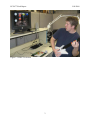
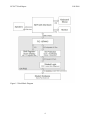


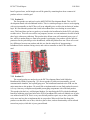

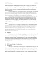
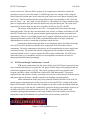
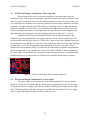


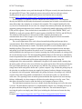

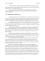

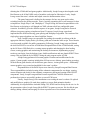
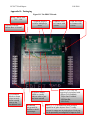
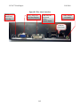

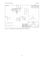
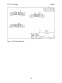
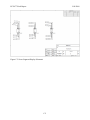
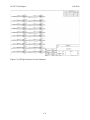


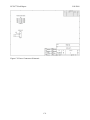
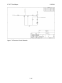


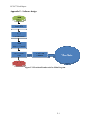
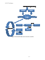
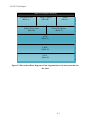


![(PDF/1,99Mo) [EN]](http://vs1.manualzilla.com/store/data/006340109_1-05a73265553ef7b20866f43badadb881-150x150.png)