1
BlueSense - Project Final Report
5
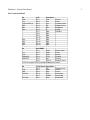
Pin Connection Detail
Z8
Gnd
Vcc
J7/Ext VREF (2)
PE3
PE1
PE2
PE4
PE5
PE6
PE7
LCD
Pin 1
Pin 2
Pin 3
Pin 4
Pin 5
Pin 6
Pin 7
Pin 8
Pin 9
Pin 10
Pin 11
Pin 12
Pin 13
Pin 14
Description
Gnd
Vcc
Vee
RS
RW
E
DB0
DB1
DB2
DB3
DB4
DB5
DB6
DB7
Ground
Power
Contrast Control
Register Select
Read/Write
Enable
Data Bus
Z8
BlueSMiRF
Pin 1
CTS-I
Clear to Send
Vcc
Pin 2
PWR
Power
Gnd
Pin 3
GND
Ground
PD4/RXD1
Pin 4
TX-O
Trasnmit
PD5/TXD1
Pin 5
RX-I
Receive
Pin 6
RTS-O
Ready to Send
*CTS-I is looped to RTS-O to disable hardware flow control.
Z8
Gnd
Vdd
PA6/SCL
PA7/SDA
Temp Sensor
Pin 1
Pin 2
Pin 3
Pin 4
Pin 5
Pin 6
Description
AS
GND
Vdd
SCL
ALERT
SDA
Address Select
Ground
Power
Serial Clock
Alert Config
Serial Data