1
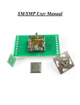
Spring Pin Socket User Manual
Tel: (800) 404-0204 • (952) 229-8200
Fax: (952) 229-8201
11351 Rupp Dr. Suite 400, Burnsville, MN 55337
www.ironwoodelectronics.com
Spring Pin Socket User Manual
Selecting a BGA Spring pin socket .............................................................................................................2
PCB Requirements .......................................................................................................................................3
Thickness ................................................................................................................................................................. 3
Finish........................................................................................................................................................................ 3
Cleanliness ............................................................................................................................................................... 3
IC and PCB Reflow Requirement...............................................................................................................3
Socket Assembly ...........................................................................................................................................4
Backing and insulation Plate .......................................................................................................................5
IC Insertion/extraction.................................................................................................................................6
1mm & 1.27mm Center - Spring Probe Specification ..............................................................................7
0.8mm Center - Spring Probe Specification ..............................................................................................7
0.5mm Center - Spring Probe Specification ..............................................................................................7
0.4mm Center - Spring Probe Specification ..............................................................................................8
Socket Maintenance .....................................................................................................................................9
Light Cleaning Procedure..........................................................................................................................10
Heat Sink Specifications ............................................................................................................................10
1
SSI.doc, Rev. A, IP
Rev. B/C/D, RP
Rev. E, VP
Tel: (800) 404-0204 • (952) 229-8200
Fax: (952) 229-8201
11351 Rupp Dr. Suite 400, Burnsville, MN 55337
www.ironwoodelectronics.com
Socket Mechanics
SS-BGA sockets provide high bandwidth in a small, cost
effective ZIF socket for prototype, test and burn-in applications.
SS-BGA socket is a simple, mechanical socket based on spring
pin technology. SS-BGA socket is a solder-less socket that can
be mounted on to a PCB using supplied hardware. The PCB
should have mounting and
alignment holes at proper
locations (see page 2 of the
drawing for recommended PCB
layout information). The typical
SS-BGA socket footprint is only
5mm larger than the maximum
IC size. It is compatible with
the
alternate
SG-BGA
(elastomer) socket footprint. If
Figure 1: Spring Pin Socket
there are pre-existing holes in
the PCB, an SS-BGA socket can
be custom designed to accommodate those holes (please call Ironwood
Tech Support @1-800-404-0204).
Figure 2: Picture of 1mm
center - Spring Pin
Figure 1 shows a typical spring pin socket. The spring pin functions as the
contactor between the IC package and the circuit board. The spring pin used in the socket is a lowresistance (<0.02Ω) connector. Figure 2 shows a picture of the 1mm center – double ended spring pin.
Double ended spring probes are primarily comprised of two plungers, barrel and spring. The spring (gold
plated music wire) is sandwiched between two plungers (gold plated hardened Beryllium Copper) inside
the barrel (gold plated Phosphor Bronze). The spring probe has high current rating (4.0A continuous,
single probe in free air @ ambient). The operating temperature range is -40° to 150° C.
The solder balls from the IC package come in contact with the crown end of spring pin. The bottom end of
spring pin contacts the circuit board pad, completing an electrical path for the signal. The socket
mechanism can be summarized as a downward force applied on the IC which compresses solder balls on
the spring probe which in turn compresses on the circuit board and thereby making electrical connection.
Selecting a BGA Spring pin socket
Please refer to the IC package drawing to select the corresponding BGA spring pin socket. Visit the
Ironwood website: www.ironwoodelectronics.com. Select the “Products” link. Next, under the “Browse”
menu, select the “GHz BGA & MLF Socket (SG, SS)” link. In the table, select the part number from the
first column which corresponds to your pin count, IC body size, array size, and pitch. The top webpage
frame will show a link to the drawing, a picture of the socket (JPEG format), and provide low-volume
price information. The drawing is a four page PDF file. The first page shows the socket cross sectional
views and the material details. The second page provides the recommended PCB layout (Note: BGA pads
2
SSI.doc, Rev. A, IP
Rev. B/C/D, RP
Rev. E, VP
Tel: (800) 404-0204 • (952) 229-8200
Fax: (952) 229-8201
11351 Rupp Dr. Suite 400, Burnsville, MN 55337
www.ironwoodelectronics.com
are not symmetrical to the mounting holes). The third page shows the compatible BGA specification. The
fourth page details backing/insulation plate dimensions. Check the BGA pattern and the following four
parameters.
1.
2.
3.
4.
IC co-planarity value should be less than or equal to that shown in the table.
Maximum total height of IC should be less than or equal to that shown in the table.
Maximum solder ball diameter of IC should be less than or equal to that shown in the table.
Maximum and minimum solder ball height should fall within the range shown in the table.
If any of the above parameters do not match, please call Ironwood Tech Support @1-800-404-0204 to
help select a socket (which may currently be in development).
PCB Requirements
Please refer to page 2 of the socket drawing for all PCB recommendations.
For IC body sizes of 30mm or below, the socket requires 4 mounting holes.
For IC body sizes of 31mm or above, the socket requires 8 mounting holes.
Two alignment holes are used in all sockets. The center for the first is 2.54mm below the upper right
mounting hole center and the second has a center dimension 5.08mm above the lower left mounting hole
center.
The BGA pattern is not symmetrical to the mounting holes. The BGA pattern is same as the one used for
the elastomer socket. It is shifted due to the fact that the wire filaments in the elastomer are at an angle
(the shift is half the elastomer thickness in the positive x-direction). The same footprint used by elastomer
socket is recommended for spring pin socket for interchangeability. Again, please refer to page 2 of the
drawing for recommended footprint.
Thickness
1.5mm minimum. This will change per customer application, environment and usage.
Finish
SnPb plating or Immersion Au or Immersion Ag. Other plating may be used but testing may be required.
Solder mask clearance over pad surface is acceptable.
Cleanliness
Isopropyl Alcohol or equivalent should be used to clean the board surface prior to attaching socket.
IC and PCB Reflow Requirement
If the same IC is used for number of cycles, crown tip on spring pin damages the Sn63Pb37 solder balls on
IC and conical tip damages HASL(hot air solder level) pads on PCB. From our test results, we recommend
reflowing IC solder balls every 10 cycles and HASL PCB every 30 cycles. Gold plated PCBs will not
need any reflows.
3
SSI.doc, Rev. A, IP
Rev. B/C/D, RP
Rev. E, VP
Tel: (800) 404-0204 • (952) 229-8200
Fax: (952) 229-8201
11351 Rupp Dr. Suite 400, Burnsville, MN 55337
www.ironwoodelectronics.com
Socket Assembly
Refer to figure 4 for graphical illustrations.
1. Install the socket base assembly onto the target PCB with the hardware (socket base screws)
provided. Because of asymmetrical tooling holes, the socket can be assembled with only one
orientation.
2. Open the clamshell lid and place BGA package (solder ball side down) into the socket. NOTE:
BGA orientation on target PCB is critical. If an IC frame (optional) is supplied, place it over the BGA
package. This IC frame may be necessary for packages which the encapsulate around the die does not
extend to the edge of the IC’s substrate.
3. Close the clamshell lid.
4. Turn the compression screw clockwise, until the compression plate makes contact with the BGA
package.
5. Turn the compression screw further so that BGA balls are compressed on the spring pins to make
contact. When turning becomes hard, full compression is achieved. Internal stops will prevent over
compression when turned by hand.
C u s t o m e r 's B G A P a c k a g e
C o m p r e s s io n
S c re w
L a tc h
S o c k e t l id
S ocke t B a se
S ocke t B a se
A s s e m b ly
C u s t o m e r's P C B
I n s u la t io n
p la te
B a c k in g p la t e
N y lo n w a s h e r
S o c k e t b a s e s c re w
Figure 4: Graphical Illustration of Socket Assembly
4
SSI.doc, Rev. A, IP
Rev. B/C/D, RP
Rev. E, VP
Tel: (800) 404-0204 • (952) 229-8200
Fax: (952) 229-8201
11351 Rupp Dr. Suite 400, Burnsville, MN 55337
www.ironwoodelectronics.com
Backing and insulation Plate
For all IC body sizes, spring pin sockets require a rigid metal backing plate to prevent deflection of the
target circuit board due to a high normal force required to compress the spring pins. If the backside of the
target PCB contains capacitors and resistors, a custom insulation plate with cavities cut for those
components can be designed. This insulation plate sandwiches between the backing plate and target PCB
as shown in figure 4. Figure 5 shows an example of a custom insulation plate.
Top view
(with component layout
reference only)
2.09mm
Top View
5.080mm±0.025mm
31.825mm ±0.025mm(x4)
2.09mm
36.00mm
2.540mm±0.025mm
36.00mm
Side View
Ø 1.59mm (x4)
Ø 0.79mm (x2)
1.59mm±0.18mm
Figure 5: Insulation Plate example drawing
5
SSI.doc, Rev. A, IP
Rev. B/C/D, RP
Rev. E, VP
Tel: (800) 404-0204 • (952) 229-8200
Fax: (952) 229-8201
11351 Rupp Dr. Suite 400, Burnsville, MN 55337
www.ironwoodelectronics.com
IC Insertion/extraction
A vacuum pen is recommended for insertion/extraction of ICs. Figure 6 shows a typical vacuum pen. TLvacuumpen-01 can be purchased separately. Hand insertion of ICs and extraction using a small tweezers is
also acceptable.
12.70mm [0.500"]
127.00mm
[5.000"]
Figure 6: Vacuum Pen with
Attachments
6
SSI.doc, Rev. A, IP
Rev. B/C/D, RP
Rev. E, VP
Tel: (800) 404-0204 • (952) 229-8200
Fax: (952) 229-8201
11351 Rupp Dr. Suite 400, Burnsville, MN 55337
www.ironwoodelectronics.com
1mm & 1.27mm Center - Spring Probe Specification
Operating Temperature
Continuous usage: -40°C to +150°C
Mechanical Specifications
Individual spring pin force
30g (1.1oz) at 0.098” (2.49mm) recommended operating position
Spring pin cycle life
500,000 cycles
Electrical Specifications
Contact resistance:
Self Inductance:
Mutual Inductance:
Cross talk:
Insertion loss:
Rise time
Pin to ground Capacitance:
Pin to pin Capacitance:
Current carrying capacity:
P-P112A / P-P138A
27.38mΩ
0.62nH
0.065nH
<-10dB to 8GHz
<0.5dB to 4.1GHz
<1 dB to 10GHz
24.6 ps
0.45pF
0.042pF
4A
P-P127A
28.19mΩ
0.70nH
4.5A
0.8mm Center - Spring Probe Specification
Operating Temperature
Continuous usage: -40°C to +120°C
Mechanical Specifications
Individual spring pin force
22g (0.8oz) at 0.162” (4.11mm) recommended operating position
Spring pin cycle life
500,000 cycles
Electrical Specifications
Contact resistance:
Self Inductance:
Insertion loss:
Pin to ground Capacitance:
Pin to pin Capacitance:
Current carrying capacity:
P-P114A
18.62mΩ
0.84nH
<1dB to 6.7 GHz
<3dB to 12 GHz
0.76pF
0.068pF
3A
0.5mm Center - Spring Probe Specification
Operating Temperature
Continuous usage: -40°C to +150°C
Mechanical Specifications
Individual spring pin force
7
SSI.doc, Rev. A, IP
Rev. B/C/D, RP
Rev. E, VP
Tel: (800) 404-0204 • (952) 229-8200
Fax: (952) 229-8201
11351 Rupp Dr. Suite 400, Burnsville, MN 55337
www.ironwoodelectronics.com
16g (0.56oz) at 0.150” (3.81mm) recommended operating position
Spring pin cycle life
500,000 cycles
Electrical Specifications
Contact resistance:
Self Inductance:
Mutual Inductance:
Cross talk:
Insertion loss:
Rise time
Pin to ground Capacitance:
Pin to pin Capacitance:
Current carrying capacity:
P-P115A / P-P139A
82.28mΩ
1.3nH
0.15nH
<-15dB to 6.5GHz
<0.25dB to 4.5 GHz
<3dB to 10 GHz
<26 ps
0.53pF
0.045pF
2.5A
0.4mm Center - Spring Probe Specification
Operating Temperature
Continuous usage: -40°C to +120°C
Mechanical Specifications
Individual spring pin force
20g (0.7oz) at operating position
Spring pin cycle life
500,000 cycles
Electrical Specifications
Contact resistance:
Self Inductance:
Insertion loss:
Pin to ground Capacitance:
Current carrying capacity:
P-P136A / P-P134A
62mΩ
1.1nH
<1dB to 11.5 GHz
<3dB to 19.3 GHz
0.58pF
1.5A
Socket Maintenance
Setting up a Preventative Maintenance Program is important in maintaining both Socket and Test Probe
life expectancy as well as good electrical continuity which will help minimize false rejects and low test
yields. Generally, light cleaning is recommended for a preventative maintenance program of the test
socket assembly. The most effective way to determine a schedule is by tracking test yields. The
maintenance schedule should be based on when yields begin to fall below the performance of a new test
socket. Some customers perform light cleanings on a per day basis or at 20,000 or 50,000 cycle intervals.
The schedule depends on the amount of debris or contamination that the socket and test probes are subject
to.
The following items should be included in a typical maintenance program.
8
SSI.doc, Rev. A, IP
Rev. B/C/D, RP
Rev. E, VP
Tel: (800) 404-0204 • (952) 229-8200
Fax: (952) 229-8201
11351 Rupp Dr. Suite 400, Burnsville, MN 55337
www.ironwoodelectronics.com
•
•
•
•
•
Regular visual inspection to identify abnormal wear and contaminants on the socket or test probes.
Examine the composition of any debris present and determine its source. Try to minimize the
source of debris if possible.
Verify that the socket is properly mounted to the load board and that it’s flush to the top surface of
the load board.
Do not use any chemicals for cleaning the socket.
Do not use any lubricants for test probe cleaning.
Light Cleaning Procedure
Required equipment needed:
• Soft to medium bristle nylon brush
• Set of screwdrivers
• Set of Hex / Allen wrenches
• Small electronics industrial vacuum
• Non-powdered latex or rubber gloves or finger cots
Cleaning Procedure
• Remove the socket from the load board and brush any debris from the solder pads of the load
board while vacuuming.
• If the socket is equipped with a manual lid remove or open it to gain access to the test probe tips.
• Hold the test socket in the vertical position, brush and vacuum at the same time to avoid any
contaminants going inside the socket or working their way into the test probe assembly. (This
operation is sometimes easier with two people)
• Rotate the socket 90 degrees and repeat the previous step.
• Brush and vacuum the socket including the nest if equipped.
• Re-assemble the socket onto the load board when cleaning is complete.
• If your test socket is to be put in storage it is recommended that the light cleaning procedure be
performed before storage so that any harmful contaminants left on the test probes do not harden
and become difficult to remove. For example solder buildup will oxidize over time and will
permanently damage probe tips.
• Always store the socket assembly in a dust free fully enclosed package.
What to avoid when cleaning
• Use of compressed air is strongly discouraged. Compressed Air will drive contaminants into the
internal working parts of the test probes.
• Do not apply solder or heat to the test probes.
• Use of alcohol or other cleaners can leave a residue and carry contaminants into the internal
working parts of the test probes.
• Repeated mechanical cleaning of the probe tips will shorten the time period between required
maintenance and more importantly it will start to remove surface plating which can result in
continuity issues as well as contact failures and elevated resistance.
9
SSI.doc, Rev. A, IP
Rev. B/C/D, RP
Rev. E, VP
Tel: (800) 404-0204 • (952) 229-8200
Fax: (952) 229-8201
11351 Rupp Dr. Suite 400, Burnsville, MN 55337
www.ironwoodelectronics.com
•
Heavy cleaning should be avoided if possible and if needed should only be performed once in the
lifetime of the test probes. Heavy cleaning can be done by using the same tools and methods as
with light cleaning with the exception of a soft brass brush being used with a very small amount of
alcohol. Remember that an excess of alcohol and heavy brushing can lead to damage as well as
unfavorable test results.
Heat Sink Specifications
For high power dissipation, a specific heat sink lid can be designed using QFIN software. Please call
Ironwood Tech Support @1-800-404-0204.
10
SSI.doc, Rev. A, IP
Rev. B/C/D, RP
Rev. E, VP