1
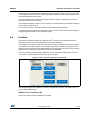
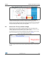
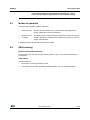
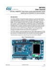
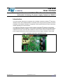
UM1832 User manual Trimming interface board USB to I2C with embedded load for automatic trimming of power supply based on SEA01 Introduction This user manual describes the operation of the STEVAL-PCC019V1 USB to I2C trimming interface board, with embedded load for automatic power supply trimming based on SEA01. Hardware and software installation is explained in the first part of the document, followed by details regarding use of the interface. The STEVAL-PCC019V1 is a tool used to interface a Windows®-based PC with digitally trimmable products like the SEA01. It is therefore essentially a bidirectional bridge between USB and I2C buses. The board also embeds an active CC/CV load to trim SEA01-based power supplies without any external instruments (such as supply, voltmeter, active load). Figure 1. STEVAL-PCC019V1 evaluation board October 2014 DocID027041 Rev 1 1/58 www.st.com 58 Contents UM1832 Contents 1 Main characteristics of the board . . . . . . . . . . . . . . . . . . . . . . . . . . . . . . 7 2 Getting started . . . . . . . . . . . . . . . . . . . . . . . . . . . . . . . . . . . . . . . . . . . . . . 8 3 4 5 6 2/58 2.1 System requirements . . . . . . . . . . . . . . . . . . . . . . . . . . . . . . . . . . . . . . . . . 8 2.2 Package contents . . . . . . . . . . . . . . . . . . . . . . . . . . . . . . . . . . . . . . . . . . . . 8 Software installation . . . . . . . . . . . . . . . . . . . . . . . . . . . . . . . . . . . . . . . . . 9 3.1 Virtual com port drivers installation (SiLabs CP2102) . . . . . . . . . . . . . . . . 9 3.2 GUI installation (using the installer) . . . . . . . . . . . . . . . . . . . . . . . . . . . . . . 9 3.3 GUI installation (without installer) . . . . . . . . . . . . . . . . . . . . . . . . . . . . . . . . 9 Hardware description and setup . . . . . . . . . . . . . . . . . . . . . . . . . . . . . . 10 4.1 Block diagram . . . . . . . . . . . . . . . . . . . . . . . . . . . . . . . . . . . . . . . . . . . . . . 10 4.2 Power supply section . . . . . . . . . . . . . . . . . . . . . . . . . . . . . . . . . . . . . . . . 10 4.3 USB to I2C bridge . . . . . . . . . . . . . . . . . . . . . . . . . . . . . . . . . . . . . . . . . . . 10 4.4 Isolation . . . . . . . . . . . . . . . . . . . . . . . . . . . . . . . . . . . . . . . . . . . . . . . . . . .11 4.5 Grounds for SEA01 ports#1 and #2 . . . . . . . . . . . . . . . . . . . . . . . . . . . . . 12 4.6 Active load: CV loop (constant voltage) . . . . . . . . . . . . . . . . . . . . . . . . . . 13 4.7 Active load: CC loop (constant current) . . . . . . . . . . . . . . . . . . . . . . . . . . 14 4.8 Thermal considerations . . . . . . . . . . . . . . . . . . . . . . . . . . . . . . . . . . . . . . 15 4.9 Anti-steady state protection . . . . . . . . . . . . . . . . . . . . . . . . . . . . . . . . . . . 15 4.10 ADC reference and calibration . . . . . . . . . . . . . . . . . . . . . . . . . . . . . . . . . 15 Running the evaluation board . . . . . . . . . . . . . . . . . . . . . . . . . . . . . . . . 16 5.1 Hardware interfaces . . . . . . . . . . . . . . . . . . . . . . . . . . . . . . . . . . . . . . . . . 16 5.2 Use of sense cables . . . . . . . . . . . . . . . . . . . . . . . . . . . . . . . . . . . . . . . . . 16 5.3 Status LEDs . . . . . . . . . . . . . . . . . . . . . . . . . . . . . . . . . . . . . . . . . . . . . . . 17 5.4 Connecting supply and trimming board together . . . . . . . . . . . . . . . . . . . 18 Running the GUI . . . . . . . . . . . . . . . . . . . . . . . . . . . . . . . . . . . . . . . . . . . 19 6.1 Connection management . . . . . . . . . . . . . . . . . . . . . . . . . . . . . . . . . . . . . 19 6.2 Power supply (basic) specifications . . . . . . . . . . . . . . . . . . . . . . . . . . . . . 20 DocID027041 Rev 1 UM1832 Contents 6.3 Modes of operation . . . . . . . . . . . . . . . . . . . . . . . . . . . . . . . . . . . . . . . . . . 21 6.4 SEA trimming . . . . . . . . . . . . . . . . . . . . . . . . . . . . . . . . . . . . . . . . . . . . . . 21 6.5 6.6 7 8 6.4.1 Voltage trimming . . . . . . . . . . . . . . . . . . . . . . . . . . . . . . . . . . . . . . . . . . 22 6.4.2 Limiting current trimming . . . . . . . . . . . . . . . . . . . . . . . . . . . . . . . . . . . . 22 6.4.3 OTP Programming operation . . . . . . . . . . . . . . . . . . . . . . . . . . . . . . . . . 22 Manual operation . . . . . . . . . . . . . . . . . . . . . . . . . . . . . . . . . . . . . . . . . . . 23 6.5.1 Example #1: the effects of voltage trimming . . . . . . . . . . . . . . . . . . . . . 24 6.5.2 Example #2: the effects of current trimming . . . . . . . . . . . . . . . . . . . . . 24 Voltage/current graph . . . . . . . . . . . . . . . . . . . . . . . . . . . . . . . . . . . . . . . . 25 6.6.1 Chart controls . . . . . . . . . . . . . . . . . . . . . . . . . . . . . . . . . . . . . . . . . . . . 27 6.6.2 Current sweep . . . . . . . . . . . . . . . . . . . . . . . . . . . . . . . . . . . . . . . . . . . . 28 6.6.3 Voltage sweep . . . . . . . . . . . . . . . . . . . . . . . . . . . . . . . . . . . . . . . . . . . . 30 Configuration . . . . . . . . . . . . . . . . . . . . . . . . . . . . . . . . . . . . . . . . . . . . . . 33 7.1 Timings . . . . . . . . . . . . . . . . . . . . . . . . . . . . . . . . . . . . . . . . . . . . . . . . . . . 33 7.2 Force SEA ground . . . . . . . . . . . . . . . . . . . . . . . . . . . . . . . . . . . . . . . . . . 33 7.3 Temperature . . . . . . . . . . . . . . . . . . . . . . . . . . . . . . . . . . . . . . . . . . . . . . . 34 Troubleshooting . . . . . . . . . . . . . . . . . . . . . . . . . . . . . . . . . . . . . . . . . . . 35 8.1 No LED activity is observed on the trimming board . . . . . . . . . . . . . . . . . 35 8.2 USB yellow LED turns off after 3 or 4 seconds . . . . . . . . . . . . . . . . . . . . 35 8.3 Voltage measurement fluctuating when using isolated SEA Port#3 . . . . . 36 8.4 Transient peak current when load is operating in CC mode on the STEVAL-ISA161V1 . . . . . . . . . . . . . . . . . . . . . . . . . . . . . . . . . . . . . . . . . 37 8.5 Supply enters protection mode during voltage trimming on the STEVAL-ISA161V1 . . . . . . . . . . . . . . . . . . . . . . . . . . . . . . . . . . . . . . . . . 37 8.6 Supply sometimes produces clicking sounds on the STEVAL-ISA161V1 38 8.7 Power supply continuously produces clicking sounds on the STEVAL-ISA161V1 . . . . . . . . . . . . . . . . . . . . . . . . . . . . . . . . . . . . . . . . . 38 9 Board schematic . . . . . . . . . . . . . . . . . . . . . . . . . . . . . . . . . . . . . . . . . . . 40 10 Board layout . . . . . . . . . . . . . . . . . . . . . . . . . . . . . . . . . . . . . . . . . . . . . . 46 11 Bill of material . . . . . . . . . . . . . . . . . . . . . . . . . . . . . . . . . . . . . . . . . . . . . 48 12 References . . . . . . . . . . . . . . . . . . . . . . . . . . . . . . . . . . . . . . . . . . . . . . . . 56 DocID027041 Rev 1 3/58 58 Contents 13 4/58 UM1832 Revision history . . . . . . . . . . . . . . . . . . . . . . . . . . . . . . . . . . . . . . . . . . . 57 DocID027041 Rev 1 UM1832 List of figures List of figures Figure 1. Figure 2. Figure 3. Figure 4. Figure 5. Figure 6. Figure 7. Figure 8. Figure 9. Figure 10. Figure 11. Figure 12. Figure 13. Figure 14. Figure 15. Figure 16. Figure 17. Figure 18. Figure 19. Figure 20. Figure 21. Figure 22. Figure 23. Figure 24. Figure 25. Figure 26. Figure 27. Figure 28. Figure 29. Figure 30. Figure 31. Figure 32. Figure 33. Figure 34. Figure 35. Figure 36. Figure 37. Figure 38. Figure 39. Figure 40. Figure 41. Figure 42. Figure 43. Figure 44. Figure 45. Figure 46. Figure 47. Figure 48. STEVAL-PCC019V1 evaluation board . . . . . . . . . . . . . . . . . . . . . . . . . . . . . . . . . . . . . . . . . 1 SEA trimming tool icon in the start program . . . . . . . . . . . . . . . . . . . . . . . . . . . . . . . . . . . . . 9 Block diagram of the STEVAL-PCC019V1 board . . . . . . . . . . . . . . . . . . . . . . . . . . . . . . . . 10 The 3 electrical domains of the board. . . . . . . . . . . . . . . . . . . . . . . . . . . . . . . . . . . . . . . . . 11 Connection for SEA01 on the secondary side (isolated from mains) . . . . . . . . . . . . . . . . . 12 Connection for SEA01 on the primary side (not isolated from mains) . . . . . . . . . . . . . . . . 12 Recommended SEA01 grounding and power supply connection. . . . . . . . . . . . . . . . . . . . 13 CC/CV mode of power supply . . . . . . . . . . . . . . . . . . . . . . . . . . . . . . . . . . . . . . . . . . . . . . 13 CC/CV loop . . . . . . . . . . . . . . . . . . . . . . . . . . . . . . . . . . . . . . . . . . . . . . . . . . . . . . . . . . . . . 14 Description of the various connectors of the board . . . . . . . . . . . . . . . . . . . . . . . . . . . . . . 16 Theory of operation for sense connection . . . . . . . . . . . . . . . . . . . . . . . . . . . . . . . . . . . . . 16 Measure without sense . . . . . . . . . . . . . . . . . . . . . . . . . . . . . . . . . . . . . . . . . . . . . . . . . . . . 17 Measure with sense . . . . . . . . . . . . . . . . . . . . . . . . . . . . . . . . . . . . . . . . . . . . . . . . . . . . . . 17 Status LEDs . . . . . . . . . . . . . . . . . . . . . . . . . . . . . . . . . . . . . . . . . . . . . . . . . . . . . . . . . . . . 17 Basic setup with STEVAL-ISA161V1 board (left) and trimming board (right) . . . . . . . . . . . 18 SEA01 GUI startup screen . . . . . . . . . . . . . . . . . . . . . . . . . . . . . . . . . . . . . . . . . . . . . . . . . 19 Successful connection to SEA01 . . . . . . . . . . . . . . . . . . . . . . . . . . . . . . . . . . . . . . . . . . . . 20 SiLabs VCP in the device manager . . . . . . . . . . . . . . . . . . . . . . . . . . . . . . . . . . . . . . . . . . 20 Power supply specification box. . . . . . . . . . . . . . . . . . . . . . . . . . . . . . . . . . . . . . . . . . . . . . 20 SEA trimming tab . . . . . . . . . . . . . . . . . . . . . . . . . . . . . . . . . . . . . . . . . . . . . . . . . . . . . . . . 22 OTP programming . . . . . . . . . . . . . . . . . . . . . . . . . . . . . . . . . . . . . . . . . . . . . . . . . . . . . . . 23 Manual operation tab . . . . . . . . . . . . . . . . . . . . . . . . . . . . . . . . . . . . . . . . . . . . . . . . . . . . . 23 Manual operation: load in CC mode (playing with voltage trimming) . . . . . . . . . . . . . . . . . 24 Manual operation: load in CV mode (playing with current trimming) . . . . . . . . . . . . . . . . . 25 V/I graph tab . . . . . . . . . . . . . . . . . . . . . . . . . . . . . . . . . . . . . . . . . . . . . . . . . . . . . . . . . . . . 25 CC/CV curves for supply and load . . . . . . . . . . . . . . . . . . . . . . . . . . . . . . . . . . . . . . . . . . . 26 Legend of graph . . . . . . . . . . . . . . . . . . . . . . . . . . . . . . . . . . . . . . . . . . . . . . . . . . . . . . . . . 27 Tabular data . . . . . . . . . . . . . . . . . . . . . . . . . . . . . . . . . . . . . . . . . . . . . . . . . . . . . . . . . . . . 28 Current sweep graph . . . . . . . . . . . . . . . . . . . . . . . . . . . . . . . . . . . . . . . . . . . . . . . . . . . . . 28 Supply load regulation . . . . . . . . . . . . . . . . . . . . . . . . . . . . . . . . . . . . . . . . . . . . . . . . . . . . 29 Zooming on current limitation . . . . . . . . . . . . . . . . . . . . . . . . . . . . . . . . . . . . . . . . . . . . . . . 30 Tabular data of supply in limitation mode . . . . . . . . . . . . . . . . . . . . . . . . . . . . . . . . . . . . . . 30 AutoDetect feature of current sweep . . . . . . . . . . . . . . . . . . . . . . . . . . . . . . . . . . . . . . . . . 30 Voltage sweep (graph and tabular). . . . . . . . . . . . . . . . . . . . . . . . . . . . . . . . . . . . . . . . . . . 32 Configuration window . . . . . . . . . . . . . . . . . . . . . . . . . . . . . . . . . . . . . . . . . . . . . . . . . . . . . 33 Fuse location . . . . . . . . . . . . . . . . . . . . . . . . . . . . . . . . . . . . . . . . . . . . . . . . . . . . . . . . . . . 35 Disabling USB suspend mode of CP2102 . . . . . . . . . . . . . . . . . . . . . . . . . . . . . . . . . . . . . 36 Closing AC currents between isolated domain and main domain. . . . . . . . . . . . . . . . . . . . 36 Detail of the Y cap implementation . . . . . . . . . . . . . . . . . . . . . . . . . . . . . . . . . . . . . . . . . . . 37 Transient during CC mode operation (CC= 2 A; left:CV=18 V; right CV=12 V) . . . . . . . . . 37 Snapshot of supply going into OVP mode . . . . . . . . . . . . . . . . . . . . . . . . . . . . . . . . . . . . . 38 Power supply section . . . . . . . . . . . . . . . . . . . . . . . . . . . . . . . . . . . . . . . . . . . . . . . . . . . . . 40 MCU section . . . . . . . . . . . . . . . . . . . . . . . . . . . . . . . . . . . . . . . . . . . . . . . . . . . . . . . . . . . . 41 CC-CV loop. . . . . . . . . . . . . . . . . . . . . . . . . . . . . . . . . . . . . . . . . . . . . . . . . . . . . . . . . . . . . 42 SEA01 interface and isolation. . . . . . . . . . . . . . . . . . . . . . . . . . . . . . . . . . . . . . . . . . . . . . . 43 ADC reference and calibration . . . . . . . . . . . . . . . . . . . . . . . . . . . . . . . . . . . . . . . . . . . . . . 44 Mechanics. . . . . . . . . . . . . . . . . . . . . . . . . . . . . . . . . . . . . . . . . . . . . . . . . . . . . . . . . . . . . . 45 Top side (component side) . . . . . . . . . . . . . . . . . . . . . . . . . . . . . . . . . . . . . . . . . . . . . . . . . 46 DocID027041 Rev 1 5/58 58 List of figures Figure 49. Figure 50. 6/58 UM1832 Bottom side . . . . . . . . . . . . . . . . . . . . . . . . . . . . . . . . . . . . . . . . . . . . . . . . . . . . . . . . . . . . . 46 Assembly plan (component side) . . . . . . . . . . . . . . . . . . . . . . . . . . . . . . . . . . . . . . . . . . . . 47 DocID027041 Rev 1 UM1832 1 Main characteristics of the board Main characteristics of the board Bidirectional communication between PC (USB) and SEA01 (I2C). Self-powered from the USB line. On-board 19 V generation for SEA programming Electrical isolation between USB and the other circuitry on the board Three I2C buses running at 100 kHz, including one which is electrically isolated from the active load (if the SEA01 is on the primary side) Integrated electronic active load with sink capabilities of up to 25 V/10 A Self-calibrated references Voltage and current measurement with precision of 0.1% (voltage) and 1% (current) Integrated temperature sensor to monitor load temperature DocID027041 Rev 1 7/58 58 Getting started UM1832 2 Getting started 2.1 System requirements To use the STEVAL-PCC019V1 board, a PC with Windows® operating system must be used. The GUI (graphical user interface) works with Microsoft Windows XP, Windows 7 or later and .NET Framework 2. Note: The .NET Framework 2 is installed by default on all Windows XP (or later) operating systems, so it is not included in the installation package. 2.2 Package contents The STEVAL-PCC019V1 includes the following items: 8/58 Hardware: – Trimming interface and load demo board, also referred to as the Trimming Board later in this document – USB A to USB mini-B cable – 4-wire flat cable for target connection to SEA01 board Software: – USB drivers – PC GUI installation package Documentation: – User manual – Data brief DocID027041 Rev 1 UM1832 3 Software installation Software installation To use the STEVAL-PCC019V1, first install the USB driver and the PC GUI. 3.1 Virtual com port drivers installation (SiLabs CP2102) First install the USB drivers. Install either: CP210xCVCPInstaller_x86.exe (for 32-bit OS) CP210xCVCPInstaller_x64.exe (for 64-bit OS) Alternatively, the latest driver versions can be downloaded from the SiLabs web site http://www.silabs.com/products/mcu/Pages/USBtoUARTBridgeVCPDrivers.aspx When the trimming board is subsequently plugged into the PC, the driver is automatically installed on the system. 3.2 GUI installation (using the installer) Launch “setup.exe” and follow the installation wizard instructions. The GUI is installed by default under C:\Program Files (x86)\SMicroelectronics\SEA Trimming Tool 1.1\ Figure 2 shows the GUI icon created in the Start menu, under STMicroelectronics\SEA Trimming Tool. Figure 2. SEA trimming tool icon in the start program Note: Any previously installed versions of the software must first be uninstalled with the uninstall feature in Windows Control Panel. 3.3 GUI installation (without installer) If the user does not want to use the installer, the GUI executable and DLL files are also available. Copy the two files to a local folder Create a shortcut pointing to the executable on the local folder “SEATool.exe” DocID027041 Rev 1 9/58 58 Hardware description and setup UM1832 4 Hardware description and setup 4.1 Block diagram Figure 3. Block diagram of the STEVAL-PCC019V1 board STM32F3 MCU GPIOs Isolation I²C #2 I²C #1 I2C buses Voltage Ref. +5V I²C #3 LEDs Resistive Divider ADC_V SEA01 Trimmable Reference +24V DAC_VTARGET Isolated Supply USB 5V/24V LOAD_EN UART USB/UART bridge CV Loop Power NMOS Anti-Steadystate protection DAC_ILIM CC Loop ADC_I Opto Isolation I2C bus Power Supply Shunt T°C Sensor STEVAL-PCC019V1 4.2 Power supply section The STEVAL-PCC019V1 is self-supplied through the USB connector 5 V supply. This voltage directly supplies U18 and related circuitry. Three isolated DC-DC modules (U20, U22 and U23) are used to provide the correct supplies to the remaining part of the board, maintaining the isolation between the PC and target sides. U20: 5 V to 5 V and 15 V: MCU (5 V then 3V3) and the CCCV circuitry U22: 5 V to +24 V: voltage for burning operation for port #1 and #2 U23: 5 V to +24 V: voltage for burning operation for port #3 OTP burning operation The trimming board is also able to provide the target device with a sufficient Vcc voltage for burning. If the Vcc on the target device is less than17 V, the programming Vcc can be simply connected to the target Vcc with a couple of OR-ing diodes. Note: On STEVAL-PCC019V1 series diodes D8 and D9 are already implemented. The 19 V supply current delivered is limited to 100 mA by the on-board LDOs U11 and U14. 4.3 USB to I2C bridge Communication between the STEVAL-PCC019V1 and the PC is managed by the latter as a standard serial peripheral: the IC U18 converts the USB connection into a virtual COM port (refer to the Section 9: Board schematic). 10/58 DocID027041 Rev 1 UM1832 Hardware description and setup The RX and TX signals are then isolated using opto-couplers U16 and U19 and connected to the STM32 microcontroller U8, ensuring that the USB port and the remaining parts of the board are isolated from the mains. The microcontroller is the heart of the system and is in charge of performing conversion between UART and I2C protocols. The STM32 manages the UART to I2C conversion, for bidirectional communication between the PC and the target device. The I2C speed is set to 100 KHz (maximum speed allowed by the SEA01). A yellow LED placed near the mini-B USB connector turns on when the CP2102 has been recognized (enumerated) by the operating system. 4.4 Isolation The galvanic isolation between the USB side and I2C side is very important because it allows the target to have any potential without electrical problems. For example, if the SEA01 is placed on the primary side of an SMPS, its ground is directly connected to the rectified mains. If the interface board has no isolation, the ground of the USB connector (connected to the earth inside the PC) will cause a short circuit on a rectifier bridge diode, damaging the SMPS and the connected hardware. In order to fulfill all possible SEA01 application needs, the board embeds three I2C ports, one of which is also isolated from the main domain by U12. Figure 4. The 3 electrical domains of the board This allows trimming of the SEA01 in various configurations (primary, secondary side), or even multiple SEA01 chips. SEA01 on the secondary side In this case, either Port#1 or Port#2 can be used. DocID027041 Rev 1 11/58 58 Hardware description and setup UM1832 Figure 5. Connection for SEA01 on the secondary side (isolated from mains) STEVAL-PCC019V1 domains USB domain Main domain CP2102 USB/UART Bridge STM32 MicroController Isolated domain Supply Rectifier + Cap Transfor mer Switching MOS Rectifier + Cap Control IC CC/CV Load SEA Port#1 SEA01 SEA Port#2 SEA Port#3 Opto Primary Secondary SEA01 on the primary side In this case, Port#3 must be used; otherwise, the primary and secondary of the power supply are connected together, which would cause a lack of galvanic isolation and safety requirements, and perhaps even damage the boards. Figure 6. Connection for SEA01 on the primary side (not isolated from mains) STEVAL-PCC019V1 domains USB domain Main domain CP2102 USB/UART Bridge STM32 MicroController Isolated domain Supply Rectifier + Cap Transfor mer Switching MOS Rectifier + Cap Control IC CC/CV Load SEA Port#1 SEA01 SEA Port#2 4.5 SEA Port#3 Secondary Primary Grounds for SEA01 ports#1 and #2 As mentioned above, the SEA01 ports #1 & #2 share the same domain as the load. This means the SEA01 grounds and active load are connected together. Conversely, on the STEVAL-ISA161V1: the main ground is connected to the STEVAL-PCC019V1 board the SEA01 ground is connected before Rsense Hence if we connect the grounds, the Rsense shunt is short-circuited, which interferes with the current measurement. 12/58 DocID027041 Rev 1 UM1832 Hardware description and setup Figure 7. Recommended SEA01 grounding and power supply connection In order to avoid this situation, the ground of the 4-wire connector is not connected by default (we assume the ground connection is made through the supply ground). However, if the user wants to have a ground connection on the SEA01, this is still possible without changing the hardware thanks a small signal NMOS (Q15) controlled by a GPIO. The GPIO is controlled in the GUI advanced configuration. 4.6 Active load: CV loop (constant voltage) While trimming the output voltage is straightforward (just measure the supply output voltage), trimming of the current limitation is more complex. You can increase the current until the voltage drops, but this process is quite long and uncertain. The easiest way is to use an active load asserted on the output voltage: when the supply enters current limitation mode, its output voltage decreases (see Figure 8). Figure 8. CC/CV mode of power supply In Figure 9, the CV loop (U5A) increases the current (by increasing Q7 gate voltage) until the supply voltage reaches the desired target voltage (typically 80-90% of nominal output voltage). DocID027041 Rev 1 13/58 58 Hardware description and setup UM1832 Figure 9. CC/CV loop The desired target voltage is set by a 12-bit DAC from the STM32; the target voltage range is between 0 and 26 V, with 6.4 mV/LSB. Note: - The absolute precision of the target voltage is not designed to be precise (it is governed by the DAC 0.5% gain error, resistive dividers of the loop, etc.) - The CV loop is mainly used to measure the limiting current, and the CV voltage has very limited influence in this case. - The ADC voltage measurement, on the other hand, has a precision of 0.1%. 4.7 Active load: CC loop (constant current) Another loop is the constant current (CC) loop, designed to: protect the board in case of overcurrent sink a given current from the supply (so the supply operates in CV mode) This loop is built around U5B, which compares the current (measured on R36 shunt) and the target current set the by the BB. If the current is higher, U5B/Q9 artificially decreases the feedback voltage of the CV loop, thus U5A lowers the gate voltage of Q7 until the current reaches the target limit of the MCU. The load limiting current is set by a 12-bit DAC from the STM32; the limiting current range is between 0 and 33A (DAC full range), but the board is sized up to 10A. Resolution is 8 mA/LSB. The MCU is informed when the load is operating in constant current mode: the output voltage of U5B (comparator) is connected to Q13 wired in open collector and connected to a MCU GPIO. Thus the GPIO is low when the loop is in CC mode. Note: - As with the voltage, the absolute precision of the load limiting current is not designed to be precise (it is governed by the DAC 0.5% gain error; precision of the loop, etc.) - The CC loop is mainly used to limit current; during the current sweep operation, the current considered is the measured current, not the limiting current target (obviously they’re very close). - The current ADC, on the other hand, is designed to be 1% precise. 14/58 DocID027041 Rev 1 UM1832 4.8 Hardware description and setup Thermal considerations The power delivered by the power supply is dissipated by the MOS and shunt, mounted together on a heat sink. The STEVAL-ISA161V1 delivers 3.5 A/19 V, so the power dissipated in the load is approximately 3.5 A*19 V = 66.5 W. The heat sink on the board has a limited thermal resistance Rth = 10 °K/W in order to minimize cost/size of the board. This implies a temperature of 25° + 66.5 * 10 = 690° in steady state conditions. Obviously far above the maximum junction temperature. Actually, the heat sink can sustain 80 W during 25 s steady state operation, thus reaching a temperature of 90 °C. In order to limit the temperature, all the measurements are burst (load is engaged, measurement is performed, load is shutdown), with the maximum on-time being in the order of 1 s. The temperature of the load is also monitored by the firmware and the GUI to ensure it does not exceed a given threshold (typ. +60 °C, settable by software). 4.9 Anti-steady state protection As mentioned above, all measurements are burst. The MCU enables/disables the load in order to keep the heat sink temperature inside a “reasonable” range. A hardware safety mechanism based around Q10 is implemented on the board to prevent the load being engaged for more than 1 s (e.g., if the CPU is stalled). 4.10 ADC reference and calibration The STM32F3 series embeds 16-bit sigma-delta ADCs (SDADC). The reference voltage of the SDADC is provided by a shunt voltage generator, D1, which delivers 1.225 V ± 0.1%. However, the internal analog front-end (amplifiers) before the SDADC needs to be calibrated. Each channel (V and I) is therefore connected to a mux (U1 and U2) in order to measure a reference voltage. The reference voltage to be measured is provided by U4 in order to select 10% or 90% of the SDADC reference voltage. This calibration process is only run once, when the GUI connects with the board. DocID027041 Rev 1 15/58 58 Running the evaluation board UM1832 5 Running the evaluation board 5.1 Hardware interfaces Figure 10. Description of the various connectors of the board 5.2 Use of sense cables Given the amount of current, we highly recommend using sense connection. Figure 11. Theory of operation for sense connection 16/58 DocID027041 Rev 1 UM1832 Running the evaluation board Consider 5 A going through a cable of 1.5 mm² section over a length of 50 cm: if the resistance of the cable is 6 mΩ, the IR drop across the cable is 2*R*I = 60 mV! 60 mV represents 0.3% of the error, which is more than one trimming step of the SEA01! To alleviate this issue, the board has dedicated sense inputs for measuring voltage at the supply connection so the IR drop of the cable does not disturb the voltage measurements. If the user does not want to use sense connection, the sense and force signal must be shorted as in Figure 12; otherwise the board will not operate correctly. Figure 12. Measure without sense 5.3 Figure 13. Measure with sense Status LEDs The status of the board is given by three LEDs. Figure 14. Status LEDs Table 1. LED status definition LED & color Status D1 / Green MCU firmware OK D2 / Green Connection with SEA01 established D3 / Red Unused DocID027041 Rev 1 17/58 58 Running the evaluation board 5.4 UM1832 Connecting supply and trimming board together See Figure 15 for a typical setup of the STEVAL-PCC019V1 board connected to the STEVAL-ISA161V1: 1. connect the trimming board to a PC with the USB cable 2. connect the target device (SEA01 board) with the 4-wire flat cable to the trimming board 3. connect the power supply terminal to the load (see Section 4.2) 4. connect the mains to the power supply board Figure 15. Basic setup with STEVAL-ISA161V1 board (left) and trimming board (right) Be sure that the target device is correctly supplied. Note: the green LED D1 turns on when the MCU has booted and the board is supplied by the USB power the yellow LED D4 turns on when the USB-UART bridge is correctly recognized by the PC. If this is the first time a CP210x SiLabs USB-UART bridge driver is installed on the system, it will first install the drivers Run the SEA01 GUI software on the PC. 18/58 DocID027041 Rev 1 UM1832 6 Running the GUI Running the GUI The first screen that appears is shown in Figure 16. Figure 16. SEA01 GUI startup screen The GUI is divided in 3 areas: 6.1 Connection management: used to manage connection with the trimming board and the SEA01 chip Power supply area: all controls related to the SEA01-based supply (nominal specification, trimming controls) Trimming board area: control of the active load Connection management The GUI automatically detects the COM port to be used (the GUI selects the CP2102 based VCP). First, we establish connection with the trimming board: click “connect to IF board” the firmware performs ADC voltage and current calibration (takes 2 s approx.) If connection is successfully established, the rest of the GUI becomes undimmed and the status bar reads “connected to IF board” The next step is to communicate with the trimming IC select the SEA01 port where the trimming IC is connected click “connect to trimming IC” the system looks for a known trimming IC and displays its reference and the associated I2C address in the status bar, see Figure 17 The firmware revision of the trimming board is also displayed in the right corner DocID027041 Rev 1 19/58 58 Running the GUI UM1832 Figure 17. Successful connection to SEA01 If the GUI does not find a SiLabs based VCP, an error message pops-up. Check Device Manager to ensure the SiLabs VCP is correctly recognized: Click +Pause, and select Device Manager (see Figure 18) Figure 18. SiLabs VCP in the device manager 6.2 Power supply (basic) specifications The GUI must have a nominal power supply specification. These values are used as the target for the trimming operation, see Figure 19. The default values match the STEVAL-ISA161V1 board, i.e. 19 V/3.75 A. Figure 19. Power supply specification box Warning: 20/58 Be sure to select the voltage and current that match the power supply used. - Effectively, the SEA01 range is +/-3% for voltage and ±50% DocID027041 Rev 1 UM1832 Running the GUI - If the target voltage/current exceed this window (e.g. 12 V or 5 A), it will obviously be impossible to trim the power supply. 6.3 Modes of operation There are three possible modes of operation: SEA trimming the GUI trims the SEA01 chip in order to meet the target power supply voltage and current specification Manual control this allows tuning of both the SEA01 target chip and the active load V/I graph the GUI displays the voltage/current graph so the user can view the supply characteristics Following sections will describe each mode in details. 6.4 SEA trimming How to activate SEA trimming Go to the main tab and click the SEA trimming button. Figure 20 shows the trimming tab environment. Chip status This box indicates: the actual V/I trimming parameter used the number of OTP fuse operations available (SEA01 can only be trimmed twice) DocID027041 Rev 1 21/58 58 Running the GUI UM1832 Figure 20. SEA trimming tab 6.4.1 Voltage trimming The only parameter is the load current under which voltage calibration is performed. To perform voltage trimming without a load, un-check the “use load” check box. Otherwise, check the box and specify the load current (% of nominal voltage) used for voltage trimming. Then, click the “TrimV” button. Once the trimming is achieved, the status box displays the voltage trimming step and the associated effective voltage. 6.4.2 Limiting current trimming As discussed in Section 4.6, the load operates in CV mode for supply current trimming. Specify the ratio of the nominal voltage used during current trimming; the ratio must be between 50% and 95%. Then, click the “TrimI” button. Once the trimming is achieved, the status box displays the current trimming step and the associated effective limitation current. 6.4.3 OTP Programming operation Once voltage and current have been trimmed, the user can program the trim value in the SEA01 chip, see Figure 21. Note: 22/58 The SEA01 OTP fuse operation requires Vcc to be greater than 17 V; if the SEA01 Vcc (hence nominal voltage of the supply) is lower than this value, the on-board supply generating 19 V can be enabled by activating the “SEA external power supply” check box. DocID027041 Rev 1 UM1832 Running the GUI Figure 21. OTP programming 6.5 Manual operation How to set manual operation Go to the main tab, and click the active load control button Manual operation (See Figure 22) is perhaps the most interesting mode because you can play with the SEA01 and the active load as if you were using real laboratory instruments. Figure 22. Manual operation tab SEA controls The user can dynamically change the V/I trimming values of the SEA01 or reload the original V/I trimming values stored in the OTP. Active load control The user can dynamically change the active load control: Voltage Target – this is the target the CV loop will try to reach Current Limitation – this is the limiting current of the load DocID027041 Rev 1 23/58 58 Running the GUI 6.5.1 UM1832 Example #1: the effects of voltage trimming See Figure 23: Note: Set a “reasonable” current limit, let’s say 200 mA; this will allow the dissipation of very low power into the load (19*0.2=3.8 W), hence long operating time The Voltage Target value does not have any influence: the CC loop of the load effectively limits the current, so the CV loop has no influence Play with the VrefV trimming knob of the SEA01box and observe the variations in the output voltage The load is operating in CC mode, as expected (187 mA measured for 200 mA target). Figure 23. Manual operation: load in CC mode (playing with voltage trimming) 6.5.2 Example #2: the effects of current trimming See Figure 24: Note: 24/58 Set a “reasonable” voltage for VTarget, typically 1 or 2 V below the nominal voltage (e.g. 19-2 = 17 V). Set limit above the expected current limitation of the supply (e.g., 6 A), it does not impact the measurement as the current is limited by the supply itself this time. Play with the IrefV Trimming knob of the SEA01box and observe the variations in the current limitation. The load is operating in CV mode: 16.899 V measured for a target of 17 V. DocID027041 Rev 1 UM1832 Running the GUI Figure 24. Manual operation: load in CV mode (playing with current trimming) Warning: 6.6 Do not maintain these load conditions for too long, as the power dissipated by the load in this case is 17*3.7 A = 63 W! The GUI will automatically disable the load when the heat sink temperature reaches 60 °C, but it is better to avoid stressing the load. Voltage/current graph This feature plots a voltage vs. current graph by performing a current or voltage sweep, providing a very convenient graphical view of the supply behavior (see Figure 25). Figure 25. V/I graph tab DocID027041 Rev 1 25/58 58 Running the GUI UM1832 Current or voltage sweep As already explained, we can either perform a current or voltage sweep. See Figure 26. Table 2. CC/CV operating mode on supply/load side Supply Load Curve Remark Constant voltage (CV) Constant current (CC) Blue “Normal” working area of the supply Constant current (CC) Constant voltage (CV) Red Limiting current area of the power supply Figure 26. CC/CV curves for supply and load Note: 26/58 To ensure maximum speed, all the measurements are first collected by the firmware and then sent to the PC. This is why it may take some time between when the measurement begins and the graph is shown. DocID027041 Rev 1 UM1832 6.6.1 Running the GUI Chart controls The graphical chart has some very useful tools. The main operations are: Table 3. Chart Control using keypad and mouse Action Effect Single click Full view (0V-0A / Max V-MaxI) Ctrl + click and select area Zoom on selected Area Mouse wheel Zoom in/zoom out (center of the chart) Mouse wheel click Full screen Move mouse on a data point Display V/I measurements (green box) Move mouse on the grid Display V/I value (yellow box) If the “clear before” box is checked, each time a new measurement is performed, the previous data is automatically cleared; otherwise, the previous data remains displayed on the graph Multiple curves on the same chart: – when multiple data is displayed on the same graph, a new color is associated with each new set of measurements – you can show or hide sets of measurements by clicking the associated color in the legend box, see Figure 27 – for each curve, the type of sweep (CC/CV) and the conditions are displayed in the legend box Figure 27. Legend of graph Measurements in tabular form are also available in the Data tab (see Figure 28): – voltage and current are given in mV/mA – temperature is also displayed – CCLim indicates whether the load is operating in CCmode (limit) or CVmode (nothing) DocID027041 Rev 1 27/58 58 Running the GUI UM1832 Figure 28. Tabular data 6.6.2 Current sweep The user only needs to enter the start and stop and step values of the sweep, and then click the “make measurement” button. Figure 29 shows an example of current sweep observed on the STEVAL-ISA161V1 supply. We can clearly see the limiting current around 3.7 A Note: During the CC sweep, the target voltage used is set to 80% of the nominal voltage, hence 19 V*80%=15.2 V. Figure 29. Current sweep graph 28/58 DocID027041 Rev 1 UM1832 Running the GUI In Figure 30, we zoom the CV area of the supply, where we can clearly observe the supply load regulation characteristics of the STEVAL-ISA161V1 supply: between 0.5 A and 3.5 A, the output voltage drops from 19.007 V to 18.962 V hence 45 mV/3 A=15 mV/A. Figure 30. Supply load regulation It may also be of interest to zoom the current limitation area a little to observe the detailed power supply behavior. In Figure 31, we sweep the current between 3.4 A and 4.0 A with a smaller step (50 mA), and we can clearly see the current limitation is around 3.70 A This is also clear in the tabular data (see Figure 32): above 3.71 A, the current no longer increases because it is limited by the power supply itself. DocID027041 Rev 1 29/58 58 Running the GUI UM1832 Figure 31. Zooming on current limitation Figure 32. Tabular data of supply in limitation mode Note: The GUI can also detect the limiting region automatically and zoom the inflection area by checking the AutoDetect box, see Figure 33. Figure 33. AutoDetect feature of current sweep 6.6.3 Voltage sweep As already mentioned, it is also possible to perform a voltage sweep of the load. In this case, the current limitation is set to the maximum value (10 A), hence we can observe the various current protection capabilities of the supply vs. voltage. 30/58 DocID027041 Rev 1 UM1832 Running the GUI The user only needs to enter the start and stop and step values of the voltage sweep, and click the “make measurement” button Note: Vstart must always be greater than Vstop See example Figure 34, where a sweep from 20 V down to 1 V is performed and the results are shown: Note: for Vtarget above 19 V, there is no current, which is expected as the load can only sink current from the supply, so Vout is always 19 V for Vtarget around 19 V, the supply is regulating, hence operating in CV Mode below 19 V (nominal), the behavior of the STEVAL-ISA161V1 supply is a constant current at 3.710A ± 2 mA (measurement uncertainty) below 8V, the supply enters short circuit protection mode (Vcc below turn-off threshold) During CV sweep, the limitation current used is set to 10 A. DocID027041 Rev 1 31/58 58 Running the GUI UM1832 Figure 34. Voltage sweep (graph and tabular) 32/58 DocID027041 Rev 1 UM1832 7 Configuration Configuration Click the “configuration” button in the upper panel to open the Configuration window (Figure 35) and change certain configuration parameters. Figure 35. Configuration window 7.1 Timings Default timings are optimized to guarantee safe operating conditions while minimizing execution speed. Unless there is something specific to check, it is NOT recommended to change timings. Timings are defined for both graphic operations (timing controlled by MCU firmware) or manual mode (timings controlled by the PC). Table 4. Timings Parameter 7.2 Description Start (ms) Delay between load activation and first ADC measurements – this is basically in order to take into account both the supply & load loops settling time. Off (ms) This is the delay between two consecutive ADC measurements – the delay is smaller than Tstart given the fact the loops have already settled. Next (ms) Same as start, but for subsequent load activation. Average Sample Number of ADC averaging for both voltage and current measurements. Force SEA ground By default, it is assumed the SEA01 ground is grounded by the power supply (not the 4-wire flat cable) so the box is un-checked. See Section 4.5: Grounds for SEA01 ports#1 and #2 for further details. DocID027041 Rev 1 33/58 58 Configuration 7.3 UM1832 Temperature This parameter specifies the maximum heat sink temperature. Above this threshold, the system disables the load and prevents any new operation until the temperature decreases. Note: 34/58 We strongly recommend leaving this setting unchanged. DocID027041 Rev 1 UM1832 Troubleshooting 8 Troubleshooting 8.1 No LED activity is observed on the trimming board Usually, when the board is plugged onto the system: LED D1 lights up, indicating the MCU has booted and the power supply is present LED D4 then lights up, indicating the USB port has been enumerated correctly If none of the above occurs, it may be due to power supply issue: Locate Fuse F1 (near the USB connector, see Figure 36) and check the voltage between J6 ground (shield) and the right side of the fuse - if it is not 5 V +/- 10%, an overcurrent has blown the fuse Before replacing the fuse (0.5 A), try to determine the root cause Figure 36. Fuse location 8.2 USB yellow LED turns off after 3 or 4 seconds The yellow LED D4 is wired to the USB-suspend/ signal from CP2102, this means it only lights when the USB port is not in USB suspend mode. By default, under Win7/Win8, the system forces external devices into suspend mode to save power, which is what happens when the COM port is not being used. It does not mean the power supply is shut down, just that the CP2102 has entered low power mode. To avoid this, open Device Manager, select the SiLabs COM port, open the Power Management tab (see Figure 37) and un-check “allow the computer to turn off this device to save power”. DocID027041 Rev 1 35/58 58 Troubleshooting UM1832 Figure 37. Disabling USB suspend mode of CP2102 8.3 Voltage measurement fluctuating when using isolated SEA Port#3 Despite it not being necessary with the STEVAL-ISA161V1, the user may want to use the SEA isolated port#3 (see Chapter 4.4: Isolation). It this condition, the user might observe unstable voltage measurements (roughly 100-mV fluctuations). The reason is that, as Port#3 is isolated, the EMI AC currents aren’t under control and this can damage high impedance/low voltage nodes, and especially the voltage measurements! In order to avoid this, add a decoupling capacitor between GND_PRIM (the isolated ground from Port#3) and GND_STM (the ground of the microcontroller), as shown in Figure 38. Figure 39 shows an applied decoupling capacitor (4.7 nF 400 V X1Y1 is used). Figure 38. Closing AC currents between isolated domain and main domain STEVAL-PCC019V1 domains USB domain Main domain CP2102 USB/UART Bridge STM32 MicroController Isolated domain Supply Rectifier + Cap Transfor mer Switching MOS Rectifier + Cap Control IC CC/CV Load SEA Port#1 SEA01 SEA Port#2 36/58 SEA Port#3 DocID027041 Rev 1 Secondary Opto Primary UM1832 Troubleshooting Figure 39. Detail of the Y cap implementation 8.4 Transient peak current when load is operating in CC mode on the STEVAL-ISA161V1 When the load is operating in CC mode (e.g., CV_target = 18 V and CC_lim = 2 A), the eLOAD will exhibit a small transient peak current of about 200 - 300 µs for a low CV target. In some cases, the peak current can trip the OCP protection from the supply for a short duration. This is due to the CC loop limiting the current by changing the feedback of the CV loop. This is absolutely not related to the SEA01 behavior. Note: Remember also that the current is burst as the on-board heatsink is very small and unable to sustain steady-state operation. To mitigate this, the load is constantly engaged/disengaged (like in PWMs). Figure 40. Transient during CC mode operation (CC= 2 A; left:CV=18 V; right CV=12 V) 8.5 Supply enters protection mode during voltage trimming on the STEVAL-ISA161V1 If the user performs a large negative step for the voltage reference during manual trimming, the supply will go into protection mode for a small duration (typically 2.1 s at light load). DocID027041 Rev 1 37/58 58 Troubleshooting UM1832 This is expected behavior, see Figure 41, where we switch from Vref=+3% to Vref=-3%: as the output voltage is higher than the target, the L6566B switching controller detects an OVP (overvoltage condition) and enters protection mode. On the STEVAL-ISA161V1, the OVP is wired in auto-restart mode so the supply recover after approximately2 seconds. Figure 41. Snapshot of supply going into OVP mode 8.6 Supply sometimes produces clicking sounds on the STEVAL-ISA161V1 The STEVAL-ISA161V1 produces some audible clicks when it enters OCP (overcurrent protection) mode; the switching is abruptly stopped. The supply is prone to entering OCP mode when the output voltage is too low; this is possible, for instance, in manual mode, when the load is operating in CV move with a voltage target that is too low: between 8 and 12 V – the supply produces audible clicks, but will resume operation below 8 V – the switching controller supply enters OCP as soon as the load is applied In order to use the STEVAL-ISA161V1 under normal operating conditions, choose a CV voltage greater than 12 V. 8.7 Power supply continuously produces clicking sounds on the STEVAL-ISA161V1 If the STEVAL-ISA161V1 is continuously producing audible clicks, this normally signifies overcurrent protection mode. 38/58 DocID027041 Rev 1 UM1832 Troubleshooting If this occurs even when the load board is disconnected from the PC, it means the power NMOS has been damaged and presents a very low impedance (dead short) to the supply, usually when the temperature has breached the maximum rating. Even though this should not happen, it can occur when the user deliberately removes the thermal protection of the system. In this case, replace Q7 (STP160N75F3). If user needs to operate at higher power for longer periods of time, bigger heat sinks (from Fischer Electronic) with compatible footprints are available through the distribution channel (Radiospare, Ref 203-583). DocID027041 Rev 1 39/58 58 DocID027041 Rev 1 6 7 1 2 3 4 5 GND_USB R107 0R GND_USB 3 2 1 F1 0466.500NR 0.500A GSPG14102014DI1500 TAB1 TAB2 VBUS DD+ ID GND J6 UX60SC-MB-5ST I/O2#4 VBUS I/O1#6 U17 USBLC6-2P6 I/O2#3 GND I/O1#1 4 5 6 L1 120R BLM18PG121SN1D C38 100NF GND_USB VDD_P C52 100NF C65 C1206 NP GND_USB GND_USB 5V_USB 4.7K R85 1 2 3 4 5 6 7 C40 1UF DCD RI GND D+ DVDD REGIN GND_USB 5V_USB GND_USB 28 27 26 25 24 23 22 RXD TXD NC NC NC NC NC NC NC GND_PAD DTR DSR TXD RXD RTS CTS NC VBUS RST NC /SUSPEND SUSPEND NC NC GND_USB D4 YELLOW HSMY-C170 R105 330R GND VDD U19 ACPL-M61L U16 5V_USB 2 1 -VIN +VIN C53 2.2UF GND_USB 5V_USB 2 1 U23 NMK0512SC -VIN +VIN 330R R84 VDD_3V3 VDD_3V3 UART_TX 7 C42 2.2UF 25V C57 2.2UF 25V C44 2.2UF 4 2 3 6 1 +5V 5 L4 +15V 120R BLM18PG121SN1D 4 VOUT -VOUT 0V +VOUT -VOUT 0V +VOUT 4 2 3 C49 2.2UF 25V R108 6.8K 0805 5 C47 2.2UF 25V 1 C48 2.2UF 25V VDD24V_B GND_STM C46 2.2UF 25V 6 7 5 6 7 +24V 5 VOUT LD2981ABM33TR NC GND INHIBIT VIN U25 5 LD2981ABM33TR NC GND INHIBIT VIN U26 UART_RX Could be replaced by NMG0524SC(5->24V), but this is another part to procure, so currently stay with the same as below -VOUT2 +VOUT2 -VOUT1 +VOUT1 U22 NMK0512SC -VIN +VIN PC/USB Domain GND_USB 2 1 3 1 C36 100NF GND_STM 4 5 6 12V should be enought, but +5/+12 insn’t available So will use +5V & +15V GND VDD U20 NMD050515SC GND_USB 5V_USB C62 2.2UF GND_USB C54 2.2UF 21 20 19 18 17 16 15 29 U18 CP2102 4 5 6 3 1 ACPL-M61L C39 100NF GND_USB VDD_P R 83 330R GND_AL R101 0R AGND VLOAD_N VSHUNT_N AVDD_3V3 Isolated Domain *I2C3 C43 1UF C41 1UF VDD_3V3 Main Domain *I2C1 & I2C2 *CV Load *MCU GND_PRIM C56 1UF isolated 3V3 is needed for I2C bus R100 NP R98 0R R97 0R R96 0R R95 0R R87 0R R86 0R L6 120R BLM18PG121SN1D L5 120R BLM18PG121SN1D GND_STM VDD3V3_B GND_STM C55 1UF GND_AL TP9 TP10 1 40/58 1 9 8 9 10 11 12 13 14 VDD_P Board schematic UM1832 Board schematic Figure 42. Power supply section B3S-1000P SW 1 GND_STM GND_STM 1 4 GND_STM 2 3 R48 NP VDD_3V3 C20 18PF GND_STM C23 100NF VREF_SEL DAC_ILIM UART_TX UART_RX SEA_GND_EN DIGFREE_1 LED3 LED2 LED1 DAC_VTARGET nRST OSC_OUT Y2 16MHZ OSC_IN R44 330R R41 330R R40 330R X2 GND1 GND2 4 2 X1 C19 18PF D3 RED HSMH-C170 D2 GREEN HSMG-C170 1 3 C24 4.7UF AGND C25 100NF AVDD_3V3 GND_STM BC848BL Q14 D5 RED HSMH-C170 R118 10K R104 330R VDD_3V3 C21 4.7UF BOOT0 VBAT PC13 PC14-OSC32_IN PC15/OSC32_OUT PF0-OSC_IN PF1-OSC_OUT NRST VSSA/VrefVDDA/Vref+ PA0 PA1 PA2 VDD_3V3 1 2 3 4 5 6 7 8 9 10 11 12 GND_STM C22 100NF VDD_3V3 I2C_SCL_1 I2C_SDA_1 I2C_SCL_2 I2C_SDA_2 LED1 LED2 LED3 OSC_IN OSC_OUT nRST EN_LOAD BOOT0 GND_STM R42 0R 48 47 46 45 44 43 42 41 40 39 38 37 C29 100NF GND_STM C27 100NF C26 4.7UF 36 35 34 33 32 31 30 29 28 27 26 25 U8 STM32F373CCT6 PF7 PF6 PA13 PA12 PA11 PA10 PA9 PA8 PD8 PB15 PB14 VREFSD+ VDD_1 VSS_1 PB9 PB8 BOOT0 PB7 PB6 PB5 PB4 PB3 PA15 PA14 PA3 PA4 PA5 PA6 VDD_2 PB0 PB1 PB2 PE8 PE9 VSSSD/VREFSDVDDSD DocID027041 Rev 1 13 14 15 16 17 18 19 20 21 22 23 24 D1 GREEN HSMG-C170 PROG_ENB C28 4.7UF R99 0R DIGFREE_2 DIGFREE_4 DIGFREE_3 nJTRST JTDO JTDI JTCK/SW CLK JTMS/SW DIO R45 10K GND_VREF GND_VREF ADC_VN ADC_VP ADC_IN ADC_IP EN_LOAD CCLIM_INDIC VMEAS_VREF_SEL VREF_ADC_SIGDEL I2C_SDA_TEMP I2C_SCL_TEMP Could also be used for USB upgrade through DFU I2C_SDA_3 I2C_SCL_3 AVDD_3V3 PROG_ENA VDD_3V3 R46 NP 1 3 5 7 9 11 13 15 17 19 R47 NP R60 NP DIGFREE_4 DIGFREE_1 DIGFREE_2 DIGFREE_3 GND_STM JTDO nRST nJTRST JTDI JTMS/SW DIO JTCK/SW CLK R43 0R 2 4 6 8 10 12 14 16 18 20 GND_STM I/O1 I/O4 GND _GND I/O2 I/O3 6 5 4 GND_STM R61 NP U9 ESDALC6V1P6 R57 NP 1 2 3 CON-10x2 70246-2004 J1 R58 NP R52 R53 R54 R55 100R 100R 100R 100R R49 0R VDD_3V3 GND_STM R50 0R 1 3 5 7 9 11 13 15 R51 0R +15V 2 4 6 8 10 12 14 16 CON-8x2 70246-1604 J2 GND_STM GSPG14102014DI1505 +5V UM1832 Board schematic Figure 43. MCU section 41/58 58 DocID027041 Rev 1 GND_AL C18 100NF R102 0R VDD_3V3 DAC_ILIM EN_LOAD DAC_VTARGET 3 5 GND T°C VDD NC 1 2 4 R112 0R R38 10K VDD_3V3 GND_AL R113 NP Q10 BC848BL R30 10K GND_AL D6 BAS16 GND_AL ADC Logic SDA I2C i/f SCLK U7 TC74A0-3.3VAT current limit = V(I_LIM) * 3.57 280mV <=> 1A R34 22K C16 10UF 25V 1206 VDD_3V3 Allow 1s maximum turn ON CV Target = Vdac*7.9 (target 17V <=> Dac =2.14V) TP4 C66 NP R39 10K GND_AL 1 TP6 GND_AL C61 100NF 10K R23 GND_AL Q6 BC848BL Temp Sensor R25 47K I2C_SDA_TEMP I2C_SCL_TEMP 1 TP3 +15V U5A LM358AD NP C17 1 C63 2.2UF 25V GND_AL C14 10NF 2 - 3 + C11 1NF CV Loop GND_AL R31 47K R26 1K !! Warning, Q7 is Isolated from Heatsink Ground !! Mounted together on heatsink GND_AL R22 68K R21 470K 8 4 R92 100K 1 TP2 3 2 R32 4.7K R28 10K C13 330PF R33 470K 6 C15 1NF 7 U5B LM358AD Current limitation 5 + C64 NP C1206 GND_AL Current Limitation Loop Q7 STP160N75F3 R36 0.1R MP930-0.10-1% S D GND_AL C9 22UF 35V Note : Vshunt_N is referenced to GND_AL in power supply sheet (R101) Q8 BC848BL 1 G GND_AL 1 42/58 TP5 1 + R37 1.00K R109 1K R111 47K R88 1.00K GND_AL R110 2.2K GND_AL C67 10NF 1 2 Q13 BC848BL VLOAD_P Option: External Active Load VLOAD_N ForceSense- GSPG14102014DI1510 2 1 J8 GMKDS_3/2-7.62"-2 VSHUNT_N VSHUNT_P 2 1 J9 GMKDS_3/2-7.62"-2 GND_AL R35 1.00K Q9 BSS123 CCLIM_INDIC J7 GMKDS_3/2-7.62"-2 GND_AL LOAD_POS Board schematic UM1832 Figure 44. CC-CV loop PROG_ENB R75 10K 330R R80 3 1 2 3 R72 47K R67 1.00K ASDA ASCL U15 ACPL-M61L GND VDD VDD3V3_B 4 5 6 C33 100NF GND_PRIM U12 Si8400AA GND_PRIM BSDA BSCL 7 6 GND_STM Q11 BC848BL R70 10K VDD_3V3 VDD3V3_B GND_STM GND_STM GND_STM C32 100NF R103 0R VDD_3V3 R66 1.00K VDD_3V3 R63 1.00K Note : LED off == Output High == 19V disabled I2C_SDA_3 I2C_SCL_3 R74 10K PROG_ENA I2C_SDA_2 I2C_SCL_2 SEA_GND_EN I2C_SDA_1 I2C_SCL_1 R62 1.00K VDD_3V3 8 BVDD 1 AVDD AGND 4 BGND 5 VDD24V_B R76 1.00K +24V INHIBIT VIN U11 LM2931DR 5 8 100R 100R INHIBIT VIN U14 LM2931DR R79 R78 R77 1.00K GND_STM 5 8 R69 100R R68 100R GND_PRIM 1 2 3 NC/ADJ I/O4 I/O1 GND _GND I/O2 I/O3 NC/ADJ VOUT 4 1 GND_PRIM 1 2 3 6 5 4 R82 330K C58 10UF 25V VCC_PROGA VCC_PROGB C30 10UF 25V GND_PRIM R73 330K R71 22K R81 22K U13 ESDALC6V1P6 4 1 R115 NP GND_STM GND_STM Q15 BSS123 6 5 4 GND_STM I/O1 I/O4 GND _GND I/O3 I/O2 U10 ESDALC6V1P6 VOUT GND_STM R65 100R R64 100R GND GND GND GND 2 3 6 7 GND GND GND GND DocID027041 Rev 1 2 3 6 7 D8 BAS16 D10 BAS16 D9 BAS16 Note : 19V is shared between I2C1 & I2C2 !! But only one device at a time can be programmed 7-0215079-4 1 2 3 4 J5 CON-AMP-FLAT-4P 7-0215079-4 Isolated Domain *I2C3 Main Domain *I2C1 & I2C2 *CV Load *MCU 1 2 3 4 J4 CON-AMP-FLAT-4P Note GND of conenctor is not connected by default - effectively GND of SEA01 is not connected to gnd of supply (current sensing thorugh ground) 1 2 3 4 J3 CON-AMP-FLAT-4P 7-0215079-4 UM1832 Board schematic Figure 45. SEA01 interface and isolation GSPG14102014DI1515 43/58 58 44/58 DocID027041 Rev 1 Note :D7 : LM4041 from NS or ST can be used VREF_SEL VMEAS_VREF_SEL VSHUNT_N VSHUNT_P VLOAD_N VLOAD_P R14 3.9K C6 1UF VLOAD_N Ref & ADC calib can be referenced either to AGND or VLOAD_N (take into account GND current) GND_VREF AVDD_3V3 AGND R10 1K 0.05% R89 0R C8 100NF C7 100NF AGND R91 NP D11 1.22V LM4041-1.2 R13 0R R11 0R R12 NP R117/R120 : for ADC protection if needed R120 NP C4 NP R9 22K 0.05% Provision for Filtering/Scalling R117 0R R119 0R C68 1NF R17 1.2K 0.05% R16 10K 0.05% R15 1.2K 0.05% 1/200 ratio (1.2mVpp) S2 S1 IN AGND GND 3 2 Vcc D 5 U4 STG719 C60 100NF ADC Reference ADC Calibration (10%-90%) 6 4 1 AVDD_3V3 6 4 1 6 4 1 S2 S1 IN S2 S1 IN D AGND GND 3 2 Vcc D AVDD_3V3 AGND GND 3 2 Vcc C5 100NF 5 U1 STG719 C59 100NF 5 U2 STG719 AVDD_3V3 AGND Voltage Divider (1/23) VREF_ADC_SIGDEL ADC_IN ADC_IP ADC_VN ADC_VP Board schematic UM1832 Figure 46. ADC reference and calibration GSPG14102014DI1520 AGND AGND DocID027041 Rev 1 M9 SPACER_5MM SPACER_5MM HOLE_3.2MM_6 HOLE_3.2MM_6 M4 FIX2 FIX1 M17 SLICER_M3 SCREW _M3x6 SCREW _M3x6 M18 SLICER_M3 M10 M8 M24 USB-A_Mini-B USBA to Mini-B Cable, 1.5m long SCREW _M3x6 M12 M16 SLICER_M3 SPACER_5MM M11 HOLE_3.2MM_6 FIX3 M23 MicroMatch_4pt Flat Cable, 1.27mm 250mm 4 CTS MicroMatch SPACER_5MM M13 HOLE_3.2MM_6 M15 SLICER_M3 SCREW _M3x6 M14 FIX4 M22 CLIP_TO220 M2 CLIP_TO220 M21 CLIP_TO220 OPTICAL_TARGET MISC3 OPTICAL_TARGET OPTICAL_TARGET MISC2 MISC1 Thermal Paste M5 ISOLATOR_TO220 SIL PAD **Plastic** Slicer Thermal Paste SCREW _M3x10 M6 M20 SLICER_M3 GND_AL R116 0R SCREW _M3x10 M7 M19 SLICER_M3 HS1 SK480/50/SA Extruded Heatsink, 4.2 K/W , 50x28x10mm Fisch Elektronik UM1832 Board schematic Figure 47. Mechanics GSPG14102014DI1525 45/58 58 Board layout 10 UM1832 Board layout Figure 48. Top side (component side) Figure 49. Bottom side 46/58 DocID027041 Rev 1 UM1832 Board layout Figure 50. Assembly plan (component side) DocID027041 Rev 1 47/58 58 Bill of material 11 UM1832 Bill of material Table 5. Bill of material Ref Value Description C4 NP CAP NP 0603 C5 100NF CAP CER 100nF 50V X7R 0603 Murata C6 1UF CAP CER 1UF 16V X5R 0603 TAIYO YUDEN C7 100NF CAP CER 100nF 50V X7R 0603 Murata C8 100NF CAP CER 100nF 50V X7R 0603 Murata C9 22UF CAP ELEC 22UF Panasonic C11 1NF CAP CER 1nF 50V X7R 0603 Murata C13 330PF CAP CER 330pF 50V X7R 0603 C14 10NF CAP CER 10nF 25V X7R 0603 AVX C15 1NF CAP CER 1nF 50V X7R 0603 Murata C16 10UF CAP CER 10µF 25V X5R 1206 Murata C17 NP CAP NP 0603 C18 100NF CAP CER 100nF 50V X7R 0603 C19 18PF CAP CER 18pF 50V X7R 0603 C20 18PF CAP CER 18pF 50V X7R 0603 C21 4.7UF CAP CER 4.7UF 6V3 X5R 0603 C22 100NF CAP CER 100nF 50V X7R 0603 Murata C23 100NF CAP CER 100nF 50V X7R 0603 Murata C24 4.7UF CAP CER 4.7UF 6V3 X5R 0603 C25 100NF CAP CER 100nF 50V X7R 0603 C26 4.7UF CAP CER 4.7UF 6V3 X5R 0603 C27 100NF CAP CER 100nF 50V X7R 0603 C28 4.7UF CAP CER 4.7UF 6V3 X5R 0603 C29 100NF CAP CER 100nF 50V X7R 0603 Murata C30 10UF CAP CER 10µF 25V X5R 1206 Murata C32 100NF CAP CER 100nF 50V X7R 0603 Murata C33 100NF CAP CER 100nF 50V X7R 0603 Murata C36 100NF CAP CER 100nF 50V X7R 0603 Murata C38 100NF CAP CER 100nF 50V X7R 0603 Murata C39 100NF CAP CER 100nF 50V X7R 0603 Murata C40 1UF CAP CER 1UF 16V X5R 0603 TAIYO YUDEN C41 1UF CAP CER 1UF 16V X5R 0603 TAIYO YUDEN 48/58 DocID027041 Rev 1 Manufacturer Murata Murata Murata UM1832 Bill of material Table 5. Bill of material (continued) Ref Value Description Manufacturer C42 2.2UF CAP CER 2.2µF 25V AVX C43 1UF CAP CER 1UF 16V X5R 0603 TAIYO YUDEN C44 2.2UF CAP CER 2.2uF 6.3V X5R TDK C46 2.2UF CAP CER 2.2µF 25V AVX C47 2.2UF CAP CER 2.2µF 25V AVX C48 2.2UF CAP CER 2.2µF 25V AVX C49 2.2UF CAP CER 2.2µF 25V AVX C52 100NF CAP CER 100nF 50V X7R 0603 Murata C53 2.2UF CAP CER 2.2uF 6.3V X5R TDK C54 2.2UF CAP CER 2.2uF 6.3V X5R TDK C55 1UF CAP CER 1UF 16V X5R 0603 TAIYO YUDEN C56 1UF CAP CER 1UF 16V X5R 0603 TAIYO YUDEN C57 2.2UF CAP CER 2.2µF 25V AVX C58 10UF CAP CER 10µF 25V X5R 1206 Murata C59 100NF CAP CER 100nF 50V X7R 0603 Murata C60 100NF CAP CER 100nF 50V X7R 0603 Murata C61 100NF CAP CER 100nF 50V X7R 0603 Murata C62 2.2UF CAP CER 2.2uF 6.3V X5R TDK C63 2.2UF CAP CER 2.2µF 25V AVX C64 NP CAP NP 1206 C65 NP CAP NP 1206 C66 NP CAP NP 0603 C67 10NF CAP CER 10nF 25V X7R 0603 AVX C68 1NF CAP CER 1nF 50V X7R 0603 Murata D1 GREEN LED Green - 0805 Avago D2 GREEN LED Green - 0805 Avago D3 RED LED Red - 0805 Avago D4 YELLOW LED Yellow - 0805 Avago D5 RED LED Red - 0805 Avago D6 BAS16 DIODE, SWITCHING, BAS16, 85V, 0.5A, 4nS, SOT23-3 NXP D8 BAS16 DIODE, SWITCHING, BAS16, 85V, 0.5A, 4nS, SOT23-3 NXP D9 BAS16 DIODE, SWITCHING, BAS16, 85V, 0.5A, 4nS, SOT23-3 NXP D10 BAS16 DIODE, SWITCHING, BAS16, 85V, 0.5A, 4nS, SOT23-3 NXP D11 1.22V Precision MicroPower Shunt Voltage 1.22V 0.1% NS F1 0.500A FUSE 0.500A 63V SLO 1206 SMD Littelfuse DocID027041 Rev 1 49/58 58 Bill of material UM1832 Table 5. Bill of material (continued) Ref Value Description FIX1 HOLE_3.2MM_6 Through hole, drilled 3.2mm, Pad 6mm FIX2 HOLE_3.2MM_6 Through hole, drilled 3.2mm, Pad 6mm FIX3 HOLE_3.2MM_6 Through hole, drilled 3.2mm, Pad 6mm FIX4 HOLE_3.2MM_6 Through hole, drilled 3.2 mm, pad 6 mm HS1 SK480/50/SA Extruded heatsink, 4.2 K/W, 50x28x10mm Fischer Elektronik J1 CON-10x2 Conn 20p dual row, platted, 2.54mm vertical Molex J2 CON-8x2 Conn 16p dual row, platted, 2.54mm vertical Molex J3 CON-AMP-FLAT-4P Micromatch on-board connector, 4 ways AMP/TE Connectivity J4 CON-AMP-FLAT-4P Micromatch on-board connector, 4 ways AMP/TE Connectivity J5 CON-AMP-FLAT-4P Micromatch on-board connector, 4 ways AMP/TE Connectivity J6 UX60SC-MB-5ST Conn mini USB2.0 SMT HIROSE J7 GMKDS_3/2-7.62"-2 Connector, 2 way with screen, 7.62mm pitch Phoenix Contact J8 GMKDS_3/2-7.62"-2 Connector, 2 way with screen, 7.62mm pitch Phoenix Contact J9 GMKDS_3/2-7.62"-2 Connector, 2 way with screen, 7.62mm pitch Phoenix Contact L1 120R Ferrite bead120 Ω 2 A 0603 Murata L4 120R Ferrite bead120 Ω 2 A 0603 Murata L5 120R Ferrite bead 120 Ω 2 A 0603 Murata L6 120R Ferrite bead 120 Ω 2 A 0603 Murata M2 CLIP_TO220 Clip for TO220-TO247 heatsink Fischer Elektronik M4 SPACER_5MM Spacer M3, 5mm, female-female Richco M5 ISOLATOR_TO220 Heatsink electrical isolator, TO220, 0.18mm Bergquist M6 SCREW_M3x10 Screw, M3, 10mm, Cruciforme RS M7 SCREW_M3x10 Screw, M3, 10mm, Cruciforme RS M8 SCREW_M3x6 Screw, M3, 6mm, Cruciforme RS M9 SPACER_5MM SPACER M3, 5mm, Female-Female Richco M10 SCREW_M3x6 Screw, M3, 6mm, Cruciforme RS M11 SPACER_5MM SPACER M3, 5mm, Female-Female Richco M12 SCREW_M3x6 Screw, M3, 6mm, Cruciforme RS M13 SPACER_5MM SPACER M3, 5mm, Female-Female Richco M14 SCREW_M3x6 Screw, M3, 6mm, Cruciforme RS M15 SLICER_M3 Slicer, M3, with break RS M16 SLICER_M3 Slicer, M3, with Break RS M17 SLICER_M3 Slicer, M3, with Break RS 50/58 DocID027041 Rev 1 Manufacturer UM1832 Bill of material Table 5. Bill of material (continued) Ref Value Description Manufacturer M18 SLICER_M3 Slicer, M3, with Break RS M19 SLICER_M3 Slicer, M3, with Break RS M20 SLICER_M3 Slicer, M3, with Break RS M21 CLIP_TO220 Clip for TO220-TO247 heatsink Fischer Elektronik M22 CLIP_TO220 Clip for TO220-TO247 heatsink Fischer Elektronik M23 MicroMatch_4pt Flat cable, 1.27 mm 250 mm 4 CTS Micromatch TE Connectivity M24 USB-A_Mini-B USBA to Mini-B Cable, 1.5m long MISC 1 OPTICAL_TARGET Optical_target MISC 2 OPTICAL_TARGET Optical_target MISC 3 OPTICAL_TARGET Optical_target Q6 BC848BL XSTR,GEN PURP,NPN,30V,100mA,300mW,SOT-23 ON Semiconductor Q7 STP160N75F3 NMOS, 75V/120A, TO220 STMicroelectronics Q8 BC848BL XSTR,GEN PURP,NPN,30V,100mA,300mW,SOT-23 ON Semiconductor Q9 BSS123 NMOS, 100V/0.17A, SOT23 DiodesZetex Q10 BC848BL XSTR,GEN PURP,NPN,30V,100mA,300mW,SOT-23 ON Semiconductor Q11 BC848BL XSTR,GEN PURP,NPN,30V,100mA,300mW,SOT-23 ON Semiconductor Q13 BC848BL XSTR,GEN PURP,NPN,30V,100mA,300mW,SOT-23 ON Semiconductor Q14 BC848BL XSTR,GEN PURP,NPN,30V,100mA,300mW,SOT-23 ON Semiconductor Q15 BSS123 NMOS, 100V/0.17A, SOT23 DiodesZetex R9 22K RES 22K Ω 1/10W 0.05% 0603 SMD Panasonic corp R10 1K RES 1K Ω 1/10W 0.05% 0603 SMD Panasonic corp R11 0R 0.0 Ω 5% 1/10W 0603 YAGEO R12 NP RES NP 0603 R13 0R 0.0 Ω 5% 1/10W 0603 R14 3.9K 3.9K Ω 5% 0603 SMD R15 1.2K RES 1.2K Ω 1/10W 0.05% 0603 SMD Panasonic corp R16 10K RES 10K Ω 1/10W 0.05% 0603 SMD Panasonic corp R17 1.2K RES 1.2K Ω 1/10W 0.05% 0603 SMD Panasonic corp R21 470K RES 470K Ω 5% 0603 R22 68K RES 68K Ω 1/10W 5% 0603 SMD R23 10K RES 10K Ω 5% 1/10W 0603 SMD R25 47K 47K Ω 5% 1/10W R26 1K 1K Ω 5% 1/10W DocID027041 Rev 1 YAGEO Panasonic corp Panasonic corp 51/58 58 Bill of material UM1832 Table 5. Bill of material (continued) Ref Value Description Manufacturer R28 10K 10K Ω 5% 1/10W Panasonic corp R30 10K 10K Ω 5% 1/10W Panasonic corp R31 47K 47K Ω 5% 1/10W R32 4.7K RES 4.7K Ω 5% 1/10W 0603 SMD R33 470K RES 470K Ω 5% 0603 R34 22K 22K Ω 5% 1/10W Panasonic corp R35 1.00K Resistor, 1.00K Ω 1/10W 1% 0603 SMD Panasonic corp R36 0.1R RES 0.1 Ω 1% 30W CADDOCK R37 1.00K Resistor, Ω1.00K Ω 1/10W 1% 0603 SMD Panasonic corp R38 10K 10K Ω 5% 1/10W Panasonic corp R39 10K 10K Ω 5% 1/10W Panasonic corp R40 330R 330R Ω 5% 1/10W R41 330R 330R Ω 5% 1/10W R42 0R 0.0 Ω 5% 1/10W 0603 YAGEO R43 0R 0.0 Ω 5% 1/10W 0603 YAGEO R44 330R 330R Ω 5% 1/10W R45 10K 10K Ω 5% 1/10W R46 NP RES NP 0603 R47 NP RES NP 0603 R48 NP RES NP 0603 R49 0R 0.0 Ω 5% 1/10W 0603 YAGEO R50 0R 0.0 Ω 5% 1/10W 0603 YAGEO R51 0R 0.0 Ω 5% 1/10W 0603 YAGEO R52 100R 100 Ω 5% 1/10W Panasonic corp R53 100R 100 Ω 5% 1/10W Panasonic corp R54 100R 100 Ω 5% 1/10W Panasonic corp R55 100R 100 Ω 5% 1/10W Panasonic corp R57 NP RES NP 0603 R58 NP RES NP 0603 R60 NP RES NP 0603 R61 NP RES NP 0603 R62 1.00K Resistor, 1.00K Ω 1/10W 1% 0603 SMD Panasonic corp R63 1.00K Resistor, 1.00K Ω 1/10W 1% 0603 SMD Panasonic corp R64 100R 100 Ω 5% 1/10W Panasonic corp R65 100R 100 Ω 5% 1/10W Panasonic corp 52/58 DocID027041 Rev 1 Panasonic corp UM1832 Bill of material Table 5. Bill of material (continued) Ref Value Description Manufacturer R66 1.00K Resistor, 1.00K Ω 1/10W 1% 0603 SMD Panasonic corp R67 1.00K Resistor, 1.00K Ω 1/10W 1% 0603 SMD Panasonic corp R68 100R 100 Ω 5% 1/10W Panasonic corp R69 100R 100 Ω 5% 1/10W Panasonic corp R70 10K 10K Ω 5% 1/10W Panasonic corp R71 22K 22K Ω 1% 1/10W Panasonic corp R72 47K 47K Ω 5% 1/10W R73 330K 330K Ω 5% 0603 SMD R74 10K 10K Ω 5% 1/10W Panasonic corp R75 10K 10K Ω 5% 1/10W Panasonic corp R76 1.00K Resistor, 1.00K Ω 1/10W 1% 0603 SMD Panasonic corp R77 1.00K Resistor, 1.00K Ω 1/10W 1% 0603 SMD Panasonic corp R78 100R 100 Ω 5% 1/10W Panasonic corp R79 100R 100 Ω 5% 1/10W Panasonic corp R80 330R 330R Ω 5% 1/10W R81 22K 22K Ω 1% 1/10W R82 330K 330K Ω 5% 0603 SMD R83 330R 330R Ω 5% 1/10W R84 330R 330R Ω 5% 1/10W R85 4.7K RES 4.7K Ω 5% 1/10W 0603 SMD R86 0R 0.0 Ω 5% 1/10W 0603 YAGEO R87 0R 0.0 Ω 5% 1/10W 0603 YAGEO R88 1.00K RESISTOR, 1.00K Ω 1/10W 1% 0603 SMD Panasonic corp R89 0R 0.0 Ω 5% 1/10W 0603 YAGEO R91 NP RES NP 0603 R92 100K 100K Ω 5% 1/10W Panasonic corp R95 0R 0.0 Ω 5% 1/10W 0603 YAGEO R96 0R 0.0 Ω 5% 1/10W 0603 YAGEO R97 0R 0.0 Ω 5% 1/10W 0603 YAGEO R98 0R 0.0 Ω 5% 1/10W 0603 YAGEO R99 0R 0.0 Ω 5% 1/10W 0603 YAGEO R100 NP RES NP 0603 R101 0R 0.0 Ω 5% 1/10W 0603 YAGEO R102 0R 0.0 Ω 5% 1/10W 0603 YAGEO R103 0R 0.0 Ω 5% 1/10W 0603 YAGEO DocID027041 Rev 1 Panasonic corp 53/58 58 Bill of material UM1832 Table 5. Bill of material (continued) Ref Value Description R104 330R 330R Ω 5% 1/10W R105 330R 330R Ω 5% 1/10W R107 0R 0.0 Ω 5% 1/10W 0603 R108 6.8K RESISTOR, 6.8K 1/8W 5% 0 805 SMD R109 1K RES 1K Ω 5% 1/10W 0603 SMD R110 2.2K RES 2.2KΩ 1/10W 5% 0603 SMD R111 47K 47K Ω 5% 1/10W R112 0R 0.0 Ω 5% 1/10W 0603 R113 NP RES NP 0603 R115 NP RES NP 0603 R116 0R 0.0 Ω 5% 1/10W 0603 YAGEO R117 0R 0.0 Ω 5% 1/10W 0603 YAGEO R118 10K 10K Ω 5% 1/10W Panasonic corp R119 0R 0.0 Ω 5% 1/10W 0603 YAGEO R120 NP RES NP 0603 SW1 B3S-1000P SMT Tactile Switch TP2 TP Point Test TPTH-ANELLO-1MM TP3 TP Point Test TPTH-ANELLO-1MM TP4 TP Point Test TPTH-ANELLO-1MM TP5 TP Point Test TPTH-ANELLO-1MM TP6 TP Point Test TPTH-ANELLO-1MM TP9 TP Point Test TPTH-ANELLO-1MM TP10 TP Point Test TPTH-ANELLO-1MM U1 STG719 IC,ANLG SW,SPDT,6 PIN,SOT-23 STMicroelectronics U2 STG719 IC,ANLG SW,SPDT,6 PIN,SOT-23 STMicroelectronics U4 STG719 IC,ANLG SW,SPDT,6 PIN,SOT-23 STMicroelectronics 2C, Temp Senor, I -40/+125°C, 3V3 U7 TC74A0-3.3VAT U8 STM32F373CCT6 IC, MCU, RISC, 72 MHz, 256KB/32KB, TQFP-48 U9 ESDALC6V1P6 Quad TVS 3V U10 ESDALC6V1P6 Quad TVS 3V U11 LM2931DR Manufacturer YAGEO YAGEO OMRON MICROCHIP STMicroelectronics IC,VOLT REG,ADJ,100MA,8 PIN,SOIC STMicroelectronics 2C Silicon Laboratories Si8400AA U13 ESDALC6V1P6 Quad TVS 3V U14 LM2931DR IC,VOLT REG,ADJ,100MA,8 PIN,SOIC STMicroelectronics U15 ACPL-M61L 1ch Optocoupler, CMOS output, Low Power SO-5 Avago 54/58 I Silicon IC Isolator, 1kV, 1.7MHz, SO8 U12 DocID027041 Rev 1 UM1832 Bill of material Table 5. Bill of material (continued) Ref Value Description Manufacturer U16 ACPL-M61L 1ch Optocoupler, CMOS output, Low Power SO-5 Avago U17 USBLC6-2P6 USBLC6-2P6 - RESEAU DE DIODE TVS USB2 STMicroelectronics U18 CP2102 UART over USB bridge, QFN28 Silicon Labs U19 ACPL-M61L 1ch Optocoupler, CMOS output, Low Power SO-5 Avago U20 NMD050515SC Isolated Dual Output DCDC (5V->+5 & +15V) Murata U22 NMK0512SC Isolated Dual Output DCDC (5V->+12 & -12V) Murata U23 NMK0512SC Isolated Dual Output DCDC (5V->+12 & -12V) Murata U25 LD2981ABM33TR IC,VOLT REG,3.3V,100MA,5 PIN,SOT-23 STMicroelectronics U26 LD2981ABM33TR IC,VOLT REG,3.3V,100MA,5 PIN,SOT-23 STMicroelectronics U5 LM358AD Dual op amp, 1.1MHz, rail-to-rail, SO8 STMicroelectronics Y2 16MHZ XTAL,16MHZ,30PPM,10PF,5x3.2 FOX Electronics DocID027041 Rev 1 55/58 58 References 12 56/58 UM1832 References 1. SEA01 - Constant voltage and current controller with online digital trimming” http://www.st.com/web/catalog/sense_power/FM142/CL1454/SC276/PF255674 2. “L6566B - Multi-mode controller for SMPS” http://www.st.com/web/catalog/sense_power/FM142/CL1454/SC352/PF185802 DocID027041 Rev 1 UM1832 13 Revision history Revision history Table 6. Document revision history Date Revision 29-Oct-2014 1 Changes Initial release. DocID027041 Rev 1 57/58 58 UM1832 IMPORTANT NOTICE – PLEASE READ CAREFULLY STMicroelectronics NV and its subsidiaries (“ST”) reserve the right to make changes, corrections, enhancements, modifications, and improvements to ST products and/or to this document at any time without notice. Purchasers should obtain the latest relevant information on ST products before placing orders. ST products are sold pursuant to ST’s terms and conditions of sale in place at the time of order acknowledgement. Purchasers are solely responsible for the choice, selection, and use of ST products and ST assumes no liability for application assistance or the design of Purchasers’ products. No license, express or implied, to any intellectual property right is granted by ST herein. Resale of ST products with provisions different from the information set forth herein shall void any warranty granted by ST for such product. ST and the ST logo are trademarks of ST. All other product or service names are the property of their respective owners. Information in this document supersedes and replaces information previously supplied in any prior versions of this document. © 2014 STMicroelectronics – All rights reserved 58/58 DocID027041 Rev 1