1
AN<10449_1>
NXP Semiconductors
PN532 application note
2. Interfaces with the host controller
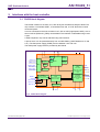
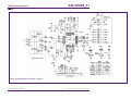
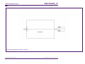
2.1 PN532 block diagram
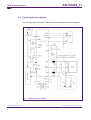
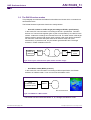
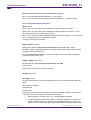
The PN532 is based on an 8051 core, with 40 Kbytes of ROM and 1Kbyte of RAM. The
chip contains a contactless UART, a contactless front end, a “PCR” block that controls
clocks and power.
It can be connected to the host controller in I2C, SPI or HSU (High Speed UART). One or
two more lines (IRQ and H_REQ) can be added. The interface is selectable using I0 and
I1 pins.
A SAM companion chip can be attached using S2C interface.
A part of the IC can be powered directly from a mobile battery (VBAT between 2.7V and
5.4V). The Pad power supply (PVDD) must be between 1.6V and 3.6V.
The SAM power supply SVDD is provided by the PN532.
P30
P31
P32 P33
IRQ
RS232
SCK or P72
MINT
ROM
40 kbyte
8051
FIFO
Power
switch, regulator,
LDO, power on reset
SVDD (output)
power for SAM interface
VDD (1.6 V to 3.6V)
VBAT (2.7 to 5.4V)
RAM
1 kbyte
ContactLess
UART
SPI
NSS or SCL
or D+ or Rx
RSTPD
I1
I2C
HSU
MISO or P71
MOSI or SDA
or D- or Tx
I0
FIFO, Mifare
Classic Unit, Frame
generation and
check
PCR
(Power Clock and
Reset controller)
ContactLess
Front End
RF Detector,
Demod, Antenna
driver
SIGIN
SIGOUT
P34
RX
LOADMOD
OSC 27.12MHz
Xtal
TX1
TX2
Fig 2. PN532 block diagram
Error! Unknown document property name.
Application note
© Koninklijke Philips Electronics N.V. 2006. All rights reserved.
Rev. <01.00> — 2006-12-15
6 of 70