1
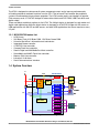
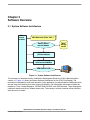
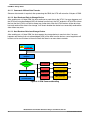
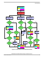
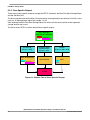
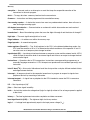
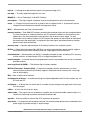
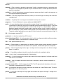
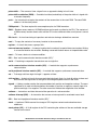
USB2.0 Card Reader
Designer Reference Manual
MC9S12
Microcontrollers
DRM065
Rev. 0.1
01/2005
freescale.com
USB2.0 Card Reader
Designer Reference Manual
by: Dennis Lui
Derek Lau
Application Engineering
Microcontroller Division
Hong Kong
To provide the most up-to-date information, the revision of our documents on the World Wide Web will be
the most current. Your printed copy may be an earlier revision. To verify that you have the latest
information available, refer to http://www.freescale.com
The following revision history table summarizes changes contained in this document. For your
convenience, the page number designators have been linked to the appropriate location.
Revision History
Date
Revision
Level
01/2005
0.1
Description
Initial release
Page
Number(s)
N/A
MC9S12UF32 Card Reader Reference Design User Manual, Rev. 0.1
Freescale Semiconductor
3
Revision History
MC9S12UF32 Card Reader Reference Design User Manual, Rev. 0.1
4
Freescale Semiconductor
Contents
Chapter 1
System Overview
1.1
1.2
1.2.1
1.2.2
1.3
1.3.1
1.4
1.4.1
1.4.2
1.4.3
1.4.4
Introduction . . . . . . . . . . . . . . . . . . . . . . . . . . . . . . . . . . . . . . . . . . . . . . . . . . . . . . . . . . . . . . . . .
System Features . . . . . . . . . . . . . . . . . . . . . . . . . . . . . . . . . . . . . . . . . . . . . . . . . . . . . . . . . . . . .
System Features . . . . . . . . . . . . . . . . . . . . . . . . . . . . . . . . . . . . . . . . . . . . . . . . . . . . . . . . . .
Cards Supported . . . . . . . . . . . . . . . . . . . . . . . . . . . . . . . . . . . . . . . . . . . . . . . . . . . . . . . . . .
MC9S12UF32 Features . . . . . . . . . . . . . . . . . . . . . . . . . . . . . . . . . . . . . . . . . . . . . . . . . . . . . . . .
MC9S12UF32 feature List . . . . . . . . . . . . . . . . . . . . . . . . . . . . . . . . . . . . . . . . . . . . . . . . . . .
System Overview . . . . . . . . . . . . . . . . . . . . . . . . . . . . . . . . . . . . . . . . . . . . . . . . . . . . . . . . . . . . .
Voltage Regulation. . . . . . . . . . . . . . . . . . . . . . . . . . . . . . . . . . . . . . . . . . . . . . . . . . . . . . . . .
Background Debug Interface . . . . . . . . . . . . . . . . . . . . . . . . . . . . . . . . . . . . . . . . . . . . . . . . .
USB Interface. . . . . . . . . . . . . . . . . . . . . . . . . . . . . . . . . . . . . . . . . . . . . . . . . . . . . . . . . . . . .
Memory Cards Interfaces. . . . . . . . . . . . . . . . . . . . . . . . . . . . . . . . . . . . . . . . . . . . . . . . . . . .
7
7
7
7
7
8
8
9
9
9
9
Chapter 2
Hardware
2.1
2.2
2.3
Introduction . . . . . . . . . . . . . . . . . . . . . . . . . . . . . . . . . . . . . . . . . . . . . . . . . . . . . . . . . . . . . . . . 11
M68EVB912UF32 . . . . . . . . . . . . . . . . . . . . . . . . . . . . . . . . . . . . . . . . . . . . . . . . . . . . . . . . . . . 11
Modifications . . . . . . . . . . . . . . . . . . . . . . . . . . . . . . . . . . . . . . . . . . . . . . . . . . . . . . . . . . . . . . . 12
Chapter 3
Software Overview
3.1
System Software Architecture . . . . . . . . . . . . . . . . . . . . . . . . . . . . . . . . . . . . . . . . . . . . . . . . . .
3.2
Main Software Flow . . . . . . . . . . . . . . . . . . . . . . . . . . . . . . . . . . . . . . . . . . . . . . . . . . . . . . . . . .
3.2.1
Main Program. . . . . . . . . . . . . . . . . . . . . . . . . . . . . . . . . . . . . . . . . . . . . . . . . . . . . . . . . . . .
3.2.1.1
USB Events Handler. . . . . . . . . . . . . . . . . . . . . . . . . . . . . . . . . . . . . . . . . . . . . . . . . . . . .
3.2.1.2
USBMS Events Handler . . . . . . . . . . . . . . . . . . . . . . . . . . . . . . . . . . . . . . . . . . . . . . . . . .
3.2.1.3
Card Insertion and Removal Handler . . . . . . . . . . . . . . . . . . . . . . . . . . . . . . . . . . . . . . . .
3.2.2
Timer Interrupt . . . . . . . . . . . . . . . . . . . . . . . . . . . . . . . . . . . . . . . . . . . . . . . . . . . . . . . . . . .
3.2.3
USB Interrupts . . . . . . . . . . . . . . . . . . . . . . . . . . . . . . . . . . . . . . . . . . . . . . . . . . . . . . . . . . .
3.3
Memory Mapping . . . . . . . . . . . . . . . . . . . . . . . . . . . . . . . . . . . . . . . . . . . . . . . . . . . . . . . . . . . .
13
14
14
14
14
14
15
15
15
Chapter 4
USB Module
4.1
4.2
4.3
4.4
Introduction . . . . . . . . . . . . . . . . . . . . . . . . . . . . . . . . . . . . . . . . . . . . . . . . . . . . . . . . . . . . . . . .
Endpoints Configurations . . . . . . . . . . . . . . . . . . . . . . . . . . . . . . . . . . . . . . . . . . . . . . . . . . . . . .
USB Device Requests . . . . . . . . . . . . . . . . . . . . . . . . . . . . . . . . . . . . . . . . . . . . . . . . . . . . . . . .
Initialization the USB Module . . . . . . . . . . . . . . . . . . . . . . . . . . . . . . . . . . . . . . . . . . . . . . . . . . .
17
17
17
18
MC9S12UF32 Card Reader Reference Design User Manual, Rev. 0.1
Freescale Semiconductor
TOC-5
Chapter 5
Intelligence QUEUE Module
5.1
5.2
Introduction . . . . . . . . . . . . . . . . . . . . . . . . . . . . . . . . . . . . . . . . . . . . . . . . . . . . . . . . . . . . . . . . 19
IQUEUE Request Mapping . . . . . . . . . . . . . . . . . . . . . . . . . . . . . . . . . . . . . . . . . . . . . . . . . . . . 19
Chapter 6
USB Mass Storage Driver
6.1
Introduction . . . . . . . . . . . . . . . . . . . . . . . . . . . . . . . . . . . . . . . . . . . . . . . . . . . . . . . . . . . . . . . .
6.2
USB Mass Storage Class Bulk-Only Transport . . . . . . . . . . . . . . . . . . . . . . . . . . . . . . . . . . . . .
6.2.1
USB Command Block Wrapper . . . . . . . . . . . . . . . . . . . . . . . . . . . . . . . . . . . . . . . . . . . . . .
6.2.2
USB Command Status Wrapper . . . . . . . . . . . . . . . . . . . . . . . . . . . . . . . . . . . . . . . . . . . . .
6.2.3
SCSI Command Descritpor Block . . . . . . . . . . . . . . . . . . . . . . . . . . . . . . . . . . . . . . . . . . . .
6.2.4
Example of Command Block Wrapper . . . . . . . . . . . . . . . . . . . . . . . . . . . . . . . . . . . . . . . . .
6.3
Driver Structure . . . . . . . . . . . . . . . . . . . . . . . . . . . . . . . . . . . . . . . . . . . . . . . . . . . . . . . . . . . . .
6.3.1
Handling of USB Command Block Wrapper . . . . . . . . . . . . . . . . . . . . . . . . . . . . . . . . . . . .
6.3.1.1
Commands Without Data Transfer. . . . . . . . . . . . . . . . . . . . . . . . . . . . . . . . . . . . . . . . . .
6.3.1.2
Host Sends out Data to Storage Device. . . . . . . . . . . . . . . . . . . . . . . . . . . . . . . . . . . . . .
6.3.1.3
Host Receives Data from Storage Device. . . . . . . . . . . . . . . . . . . . . . . . . . . . . . . . . . . . .
6.3.2
Class Specific Request . . . . . . . . . . . . . . . . . . . . . . . . . . . . . . . . . . . . . . . . . . . . . . . . . . . .
21
21
22
23
23
25
25
25
26
26
26
28
Chapter 7
Memory Cards Mass Storage Drivers
7.1
7.2
7.3
7.4
7.4.1
7.4.2
7.4.3
Introduction . . . . . . . . . . . . . . . . . . . . . . . . . . . . . . . . . . . . . . . . . . . . . . . . . . . . . . . . . . . . . . . .
RAM Mapping . . . . . . . . . . . . . . . . . . . . . . . . . . . . . . . . . . . . . . . . . . . . . . . . . . . . . . . . . . . . . .
Windows File Systems and MS/SM Data Format . . . . . . . . . . . . . . . . . . . . . . . . . . . . . . . . . . .
Memory Card Mass Storage Drivers . . . . . . . . . . . . . . . . . . . . . . . . . . . . . . . . . . . . . . . . . . . . .
Commands Without Data Transfer. . . . . . . . . . . . . . . . . . . . . . . . . . . . . . . . . . . . . . . . . . . .
Host Sends out Data to card reader. . . . . . . . . . . . . . . . . . . . . . . . . . . . . . . . . . . . . . . . . . .
Host Receives Data from Card Reader.. . . . . . . . . . . . . . . . . . . . . . . . . . . . . . . . . . . . . . . .
29
29
29
31
31
31
32
Chapter 8
Testing and Customization
8.1
Introduction . . . . . . . . . . . . . . . . . . . . . . . . . . . . . . . . . . . . . . . . . . . . . . . . . . . . . . . . . . . . . . . .
8.2
Customization . . . . . . . . . . . . . . . . . . . . . . . . . . . . . . . . . . . . . . . . . . . . . . . . . . . . . . . . . . . . . .
8.2.1
Hardware . . . . . . . . . . . . . . . . . . . . . . . . . . . . . . . . . . . . . . . . . . . . . . . . . . . . . . . . . . . . . . .
8.2.2
Firmware . . . . . . . . . . . . . . . . . . . . . . . . . . . . . . . . . . . . . . . . . . . . . . . . . . . . . . . . . . . . . . .
8.2.2.1
UF32 Card Reader Project . . . . . . . . . . . . . . . . . . . . . . . . . . . . . . . . . . . . . . . . . . . . . . . .
8.2.2.2
Mini-Kernel Project . . . . . . . . . . . . . . . . . . . . . . . . . . . . . . . . . . . . . . . . . . . . . . . . . . . . . .
35
35
35
35
35
35
Chapter 9
Glossary
MC9S12UF32 Card Reader Reference Design User Manual, Rev. 0.1
TOC-6
Freescale Semiconductor
Chapter 1
System Overview
1.1 Introduction
This manual describes a reference design of a Universal Serial Bus Card Reader solution by using the
MC9S12UF32. The software was developed under the M68EVB912UF32 evaluation platform board.
Some hardware modifications are required in order for the software to be used under the board. The
firmware source codes are available as reference materials.
1.2 System Features
1.2.1 System Features
•
•
•
USB 2.0 High Speed and Full Speed Compliance.
Windows 98 SE, Windows 2000 and Windows XP Compatible
In Circuit Evaluation and Programming
1.2.2 Cards Supported
•
•
•
•
•
•
•
CompactFlash Card (Type 1 and II)
Memory Stick
Memory Stick Duo
Magic Gate
Secure Digital
MultimediaCard
SmartMedia
1.3 MC9S12UF32 Features
The MC9S12UF32 microcontroller (hereafter referred as UF32) features an integrated Universal Serial
Bus (USB) 2.0 controller and physical layer transceivers to provide comprehensive USB specification
implementation for both high-speed (480 Mbps) and full-speed (12 Mbps) operations. The high-speed
operation, running at bus speed of 30 MHz, implements fast large data transfers for applications such as
real-time movies that were impractical at the previous lower-speed operation.
Besides standard USB functionality, the UF32 enables control of external hard disk drives, CD-ROM and
DVD-ROM drives. The UF32 also enables controls of different common Flash memory devices including:
CompactFlash, Secure Digital, MultiMediaCard, SmartMedia and Memory Stick memory cards.
The availability of up to 75 programmable I/O lines helps to minimize the system costs and enhance
flexibility.
MC9S12UF32 Card Reader Reference Design User Manual, Rev. 0.1
Freescale Semiconductor
7
System Overview
The UF32 is designed to reduce overall system components count and to improve performance by
off-loading peripheral overhead functions from the CPU. The on-board Flash enables the peripheral
system to accommodate future software upgrades. The UF32 can be used in card readers for popular
Flash memory cards, ATA/ATAPI bridges for external hard disks and DVD ROM, USB Flash disks and
digital wallets.
There are 100-pin and 64-pin options for the UF32. The 100-pin device is designed for card reader and
digital wallet applications while the 64-pin device is designed for ATA/ATAPI bridge with SD access or
USB applications with SM, SD and MS access, and other USB applications that do not require so many
I/O pins.
1.3.1 MC9S12UF32 feature List
•
•
•
•
•
•
•
•
•
•
•
HCS12 core
32K Bytes Flash, 3.5K Bytes RAM, 1.5K Bytes Queue RAM
Universal Serial Bus 2.0 controller and transceivers
Integrated Queue controller
ATA/ATAPI Host controller
CompactFlash Host controller
Secure Digital and MultiMediaCard Host controller
SmartMedia and NAND Flash Host controller
Memory Stick Host controller
8-channel, 16-bit timer
Serial Communications Interface
1.4 System Overview
5V
VDDA
MC9S12UF32
5V
VDDR
5V
3.3V
2.5V
USB
REG
2.5V
REF3V
PORTE
BDM
USB
PORTQ
PORTP
3.3V
VDD3X
3.3V
5/3.3V
VDD
SM
PORTM
SD/MMC
PORTJ
MS
PORTT
S12 Core
PORTU
PORTS
PORTR
CF
PORTB
VDDX
5/3.3V
PORTA
Figure 1-1. Block Diagram
MC9S12UF32 Card Reader Reference Design User Manual, Rev. 0.1
8
Freescale Semiconductor
System Overview
Since the UF32 is a highly integrated high-speed USB 2.0 device with embedded CF, MS, SD/MMC and
SM host controllers, the major components to implement a card reader include only a UF32, a MOSFET
for 3.3V regulation and the memory cards sockets.
The system functions can be divided into the following parts.
• Voltage regulation
• Background debug interface
• USB interface
• Memory card interfaces
1.4.1 Voltage Regulation
The UF32 is designed for a single 5V voltage input. There are three kinds of I/O:
• Port E of 5V I/O
• Port J, M, P and Q of 5V or 3.3V I/O powered by VDD3X
• Port A, B, R, S, T and U of 5V or 3.3V I/O powered by VDDX
For UF32 used in card reader applications VDDX and VDD3X are set to 3.3V. Therefore, only the Port E is
with 5V I/O while the others are with 3.3V I/O.
The UF32 has got four built-in regulators:
• 2.5V regulator for S12 core use
• 2.5V regulator for USB transceiver use
• 3.3V regulator for USB transceiver and PLL use
• 3.3V regulator that needed an external MOSFET
The S12 core is powered by the internal 2.5V regulator. The USB transceivers and PLL is powered by the
internal 3.3V regulator. The UF32 needs a 5V power supplied to VDDR . The external MOSFET is
regulated by the analog output REF3V to provide 3.3V supply to VDD3X, VDDX and to the memory cards.
1.4.2 Background Debug Interface
The single-wired background debug pin BKGD is used for software development and programming.
1.4.3 USB Interface
The UF32 featured an integrated Universal Serial Bus (USB) 2.0 controller and physical layer
transceivers. An external 1.5K pullup resistor and four serial resistors are required for USB connection.
1.4.4 Memory Cards Interfaces
The UF32 contains CF, MS, SM and SD host controller interfaces that can direct connect to the memory
cards. Only pullup and pulldown resistors are needed to connect the UF32 to the memory cards.
MC9S12UF32 Card Reader Reference Design User Manual, Rev. 0.1
Freescale Semiconductor
9
System Overview
MC9S12UF32 Card Reader Reference Design User Manual, Rev. 0.1
10
Freescale Semiconductor
Chapter 2
Hardware
2.1 Introduction
The hardware used in the reference design is based on the M68EVB912UF32 evaluation platform board.
Some hardware modifications are required in order for the software to be used under the board. Please
refer to the user manual and the schematics of the board for detail operations. The board was not
optimized design for a card reader. To implement a card reader, customer may refer to the schematic
provided in this reference design.
2.2 M68EVB912UF32
The M68EVB912UF32 evaluation platform board (hereafter referred as EVB) consists of a 100-pin
package UF32, a 12V to 5V DC-DC converter, a RS-232 transceiver and some other glue logics. It has
built-in sockets for the mass storage memory cards. Please refer to the user manual of the board for detail
operations.
Figure 2-1. M68EVB912UF32 Evaluation Board
MC9S12UF32 Card Reader Reference Design User Manual, Rev. 0.1
Freescale Semiconductor
11
Hardware
2.3 Modifications
The EVB allows the CompactFlash interface to be 5V or 3.3V by software configuration while the other
memory cards interfaces are fixed to 3.3V. Some of the card detection pins are not connected to the
UF32. The modifications are to fix the CF interface to be 3.3V and to connect the card detection pins to
the UF32.
JP10
CF_CD
JP9
JP10
SD_CD
UF32
SD_W P
W 19
JP16
MSSINS
CR5
Figure 2-2. Modifications Connections
Figure 2-2 shows the modifications required:
• Short CR5 to bypass the diode (needed for EVB of revision 5 or older version)
• Short W19 pin 1, 2 and 3
• Connect JP10 pin 5 and JP9 pin 4 for CompactFlash card detection
• Connect JP16 pin 12 and JP9 pin 5 for Secure Digital card detection
• Connect JP16 pin 14 and JP9 pin 9 for Secure Digital card write protect detection
• Connect JP16 pin 16 and JP9 pin 8 for Memory Stick card detection
MC9S12UF32 Card Reader Reference Design User Manual, Rev. 0.1
12
Freescale Semiconductor
Chapter 3
Software Overview
3.1 System Software Architecture
MiniKernel
for UF32
MCU Resources (Timer, IRQ…)
Memory Device
Interface Module
Mass
Storage
Device
Application Task
(Protocol Adapter)
USB Mass Storage
SCSI Command Module
USB Protocol Layer
Figure 3-1. System Software Architecture
The software was developed under CodeWarrior Development Studio for HC(S)12 Microcontrollers
version 3.1. Figure 3-1 shows the System Software Architecture for the UF32 Card Reader. The
mini-kernel is designed for multi-tasks operation. In this application, it mainly handles the USB event tasks
and the timer hook function tasks after system initialization. The initialization subroutines initialize the
modules of Timer, Voltage Regulator, IQUEUE RAM, IQUEUE, and USB Controller. The main program
continually checks and serves different event tasks. The memory card host controller will be initialized
after the card is inserted.
MC9S12UF32 Card Reader Reference Design User Manual, Rev. 0.1
Freescale Semiconductor
13
Software Overview
MAIN PROGRAM
TIMER INTERRUPT
USB INTERRUPTS
INITIALIZATION
CHECK AND SERVE
ANY HOOK FUNCTION
USB ENDPOINT 0
HANDLER
USB EVENTS
HANDLER
INCREASE GLOBAL TIMER
COUNTER FOR EVERY 1ms
USBMS BULK IN
HANDLER
USBMS EVENTS
HANDLER
RETURN
USBMS BULK OUT
HANDLER
CARD INSERTION &
REMOVAL HANDLER
RETURN
Figure 3-2. Main Software Flow
3.2 Main Software Flow
3.2.1 Main Program
The USB events handler puts the UF32 into suspend when USB bus suspend is detected. The USB Mass
Storage (USBMS) handler calls corresponding routines for different USBMS commands. The card
insertion and removal handler checks any card is inserted into or removed from the sockets.
3.2.1.1 USB Events Handler
The USB Events Handler puts the UF32 into STOP mode when the USB suspend is detected.
3.2.1.2 USBMS Events Handler
The USB Events Handler handles the USB Mass Storage reset and the USB Mass Storage Command
Block Wrapper.
3.2.1.3 Card Insertion and Removal Handler
The card insertion and removal handler checks any card inserted or removed from the sockets for every
100ms. The time interval is defined in the timer hook function. If any card is detected to be inserted, the
handler will enable and initialize the card host controller. If any card is detected to be removed, the handler
will disable the card host controller.
MC9S12UF32 Card Reader Reference Design User Manual, Rev. 0.1
14
Freescale Semiconductor
Memory Mapping
3.2.2 Timer Interrupt
One millisecond timer interrupt is set. It checks if there are any timer hook functions and serves them.
There are two timer hook functions: one is a 500ms hook function to flash the LED use, another is a 40ms
hook function to check the card insertion and removal. A 500ms hook function means it will be served for
every 500ms which is registered in the initialization routine.
3.2.3 USB Interrupts
There are three kinds of USB interrupts:
• Interrupts for the control Endpoint 0
• Interrupts for the Bulk IN Endpoint
• Interrupts for the Bulk OUT Endpoint
All of the interrupt events are fully handled in the interrupt routines excepts the following interrupts:
• USB suspend
• USB Mass Storage reset
• USB Mass Storage Command Block Wrapper received
The above 3 interrupt routines set some flags to indicate their presents and will then be served in the USB
or the USBMS Event Handlers in the main routine.
3.3 Memory Mapping
The memory map is configured as shown in Figure 3-3.
$0000
↓
$03FF
REGISTERS
$0400
↓
$11FF
RESERVED
$1200
↓
$1FFF
3.5K BYTES OF RAM
$2000
↓
$25FF
1.5K BYTES OF IQUEUE RAM
$2600
↓
$3FFF
RESERVED
$4000
↓
$7FFF
16K BYTES OF FLASH
$8000
↓
$BFFF
RESERVED
$C000
↓
$FEFF
16K BYTES OF FLASH
$FF00↓
$FFFF
VECTORS
Figure 3-3. Memory Map
MC9S12UF32 Card Reader Reference Design User Manual, Rev. 0.1
Freescale Semiconductor
15
Software Overview
MC9S12UF32 Card Reader Reference Design User Manual, Rev. 0.1
16
Freescale Semiconductor
Chapter 4
USB Module
4.1 Introduction
The USB Module consists of an integrated Universal Serial Bus (USB) 2.0 controller and physical layer
transceivers to provide comprehensive USB specification implementation for both high-speed (480 Mbps)
and full-speed (12 Mbps) operation.
4.2 Endpoints Configurations
Table 4-1. Endpoints Configurations
Physical
Endpoint
1
Logical
Endpoint
Transfer
Mode
Transfer
Type
Maximum Buffer
Size
0
SETUP
CONTROL
64
0
IN
CONTROL
64
0
OUT
CONTROL
64
2
1—3
IN / OUT
BULK / INT
64
3
1—3
IN / OUT
BULK / INT
64
4
1—3
OUT
ISO / BULK / INT
64 / 512
5
1—3
IN
BULK / INT
64 / 512
Table 4-1 shows the endpoints configurations. The endpoints registers in the UF32 represent the physical
endpoints. The USB host only sees the logical endpoints. The physical endpoint 0 and endpoint 1 are
mapped to the logical control endpoints 0 and no setting is needed. For the physical endpoints 2 to 5, we
need to map the used physical endpoints to the logical endpoints. The physical endpoints 2 to 5 can be
mapped to the logical endpoints 1 to 3. However, only one logical endpoint can be mapped to the logical
endpoints 3.
The maximum buffer sizes of endpoints 4 and 5 are 64 bytes at USB full-speed or 512 bytes at
high-speed. IQUEUE RAM is used as the buffers for these two endpoints. The other endpoints are
associated with delicate 64 bytes of buffers. In this application, only the control endpoints and the physical
endpoints 4 and 5 are used.
4.3 USB Device Requests
USB Device Requests are sent and completed through Control Transfer using endpoint 0. The requests
and the parameters are sent to the device in the setup packet. There are two kinds of requests. They are
called standard requests and class specific requests.
MC9S12UF32 Card Reader Reference Design User Manual, Rev. 0.1
Freescale Semiconductor
17
USB Module
The standard requests are described in the USB specification chapter 9. All of the standard requests are
handled by hardware except the get descriptor and set descriptor which are handled by firmware. In this
reference design, only the get descriptor is used.
The class specific requests are described in the individual class specifications. All need to be handled by
firmware.
4.4 Initialization the USB Module
The initialization the USB modules include enabling the 480MHz PLL and the necessary USB Endpoint 0
Interrupts, and setting the card reader as self or bus powered. The external USB 1.5K pullup resistor is
then configured to be connected to the USB D+ pin through the UF32. After detecting the pullup at the D+
pin, the host will send out a USB Reset signal to the UF32. The USB module Status Register will indicate
whether the communication setup is high-speed or full-speed. After detecting the USB reset signal, the
software can configure the USB Bulk IN and OUT endpoints, set the Queue channels for USB transmit
and receive, enable USB Bulk IN and OUT endpoint interrupts, and set the maximum buffer sizes of the
Bulk-IN and OUT endpoints depending on the USB speeds.
MC9S12UF32 Card Reader Reference Design User Manual, Rev. 0.1
18
Freescale Semiconductor
Chapter 5
Intelligence QUEUE Module
5.1 Introduction
The Intelligence Queue (IQUEUE) module allows automatic data transfer between the USB module and
IQUEUE RAM, and between IQUEUE RAM and Mass Storage Devices without CPU intervention. The
IQUEUE RAM is configured to address 0x2000 to 0x25FF by writing 0x21 to the INITEE register.
S12 CPU
USB
IQRAM
USB
IQEUE Module
IQRAM
MEMORY
CARD
IQUEUE RAM
Card
Figure 5-1. IQUEUE Module
5.2 IQUEUE Request Mapping
There are four IQUEUE channels of QC1 to QC4 which can be configured to transfer data to and from
different peripherals. QC1 is with the highest priority while QC4 is with the least priority. QC1 and QC2,
QC3 and QC4 can be configured as two double buffer channels. For IQUEUE module to transfer data
from one peripheral to another automatically, a single or double buffers channel with passing through
mode must be used. For proper operation, the USB peripheral must use the channel with higher priority.
When reading data from a memory card, QC1REQ is set to USB receive and QC2REQ is set to Memory
Card transmit. When writing data to the device, QC3REQ is set to USB transmit and QC4REQ is set to
Memory Card receive.
MC9S12UF32 Card Reader Reference Design User Manual, Rev. 0.1
Freescale Semiconductor
19
Intelligence QUEUE Module
Table 5-1. IQUEUE Request Mapping
Data Flow
QCnREQ
Peripheral
Functions
Direction
PC -> USB -> QRAM
QC1REQ = 0
USB
Rx
PC <- USB <- QRAM
QC3REQ = 1
USB
Tx
QRAM <- CF
QC4REQ = 4
CF
Rx
QRAM -> CF
QC2REQ = 5
CF
Tx
QRAM <- MS
QC4REQ = 6
MS
Rx
QRAM -> MS
QC2REQ = 7
MS
Tx
QRAM <- SD
QC4REQ = 8
SD
Rx
QRAM -> SD
QC2REQ = 9
SD
Tx
QRAM <- SM
QC4REQ = 10
SM
Rx
QRAM -> SM
QC2REQ = 11
SM
Tx
MC9S12UF32 Card Reader Reference Design User Manual, Rev. 0.1
20
Freescale Semiconductor
Chapter 6
USB Mass Storage Driver
6.1 Introduction
The driver is implemented according to the specification of the USB Mass Storage Class Bulk-Only
Transport and the specification of the Small Computer System Interface 2.
We have chosen the Bulk-Only transport rather than the Command Bulk Interrupt because the drivers for
the Bulk-Only transport are embedded in the Windows 2000 and the Windows XP. Regarding the
endpoints usage, one bulk IN and one bulk OUT endpoints together with the control endpoints are
needed. The subclass of the SCSI Transparent command 0x06 is used since the SCSI command can
support most storage and multimedia devices.
6.2 USB Mass Storage Class Bulk-Only Transport
In Bulk-Only Transport, the transfer of command, data and status occurring solely via Bulk endpoints.
There are two class specific requests through the SETUP command
• Bulk-Only Mass Storage Reset
• Get Max LUN.
The Bulk-Only Mass Storage Reset is to reset the mass storage device and its associated interface. The
GetMax LUN is used to determine the number of logical units the device supports.
The host shall send out a Command Block Wrapper through an OUT endpoint before sending out data or
requesting the device to return data. The device then responses with the Command Status Wrapper.
Figure 6-1 shows the command data status flow.
MC9S12UF32 Card Reader Reference Design User Manual, Rev. 0.1
Freescale Semiconductor
21
USB Mass Storage Driver
READY
HOST SENDS OUT CBW
OUT
DATAx 31 BYTE CBW
DEVICE RETURNS DATA
HOST SENDS OUT DATA
OUT
IN
DATAx
YES
DATA
DATAx
DATA
YES
MORE DATA
TO RECEIVE?
MORE DATA
TO SEND?
NO
NO
DEVICE RETURNS CSW
IN
DATAx 13 BYTE CSW
Figure 6-1. Command Data Status Flow
6.2.1 USB Command Block Wrapper
The host sends each Command Block Wrapper containing a command block to the device via the
Bulk-OUT endpoint. The Command Block is represented by the bits 15 to 30 of the CBW. Our device
supports the sub-class code of 0x06 of the SCSI Transparent Command Set.
Table 6-1. Command Block Wrapper
bit
Byte
0—3
7
6
5
LSB (Byte 0)
MSB (Byte 3)
4
3
2
21
0
dCBWSignature
(0x55 0x53 0x42 0x43)
4—7
dCBWTag
8 — 11
dCBWDataTransferLength (number of bytes of data transfer expected)
12
13
14
15 — 30
bmCBWFlags
Reserved (0)
Reserved (0)
bCBWLUN (logical device number)
bCBWCBLength (Command Block length)
bCBWCB (Command Block)
MC9S12UF32 Card Reader Reference Design User Manual, Rev. 0.1
22
Freescale Semiconductor
USB Mass Storage Class Bulk-Only Transport
6.2.2 USB Command Status Wrapper
The USB Command Status Wrapper starts on a packet boundary and ends as a short packet with exactly
13 bytes transferred. The bCSWStatus indicates the success or failure of the command. The device will
set this byte to zero if the command is completed successfully, to 1 if it fails and to 2 for phase error. The
host will perform a Reset Recovery when phase error status is returned in the CSW.
Table 6-2. Command Status Wrapper
7
6
5
4
3
2
0—3
dCSWSignature (0x55 0x53 0x42 0x53)
21
0
4—7
dCSWTag (get from the CBW)
8 — 11
dCSWDataResidule
(number of bytes different between expected transfer length and actual handled)
12
bmCSWStatus
6.2.3 SCSI Command Descritpor Block
The SCSI Command Descriptor Block always has an operation code as the first byte and the control byte
as its last byte. For any command, if there is an invalid parameter in the CDB, the target should terminate
the command without altering the medium.
Table 6-3. CDB of 6-byte Command
7
6
5
0
4
3
2
21
0
21
0
Operation Code
dCBWTag
1
|
3
(MSB)
Logical Block Address (if required)
(LSB)
4
Transfer Length (if required)
Parameter List Length (if required)
Allocation Length
5
Control
Table 6-4. CDB of 10-byte Command
7
6
0
1
2—5
9
4
3
2
Operation Code
Reserved (0)
(MSB byte 2)
6
7
|
8
5
Service Action (if required)
Logical Block Address (if required)
(LSB byte 5)
Reserved (0)
(MSB byte 7)
Transfer Length (if required)
Parameter List Length (if required)
Allocation length (if required)
(LSB byte 8)
Control
MC9S12UF32 Card Reader Reference Design User Manual, Rev. 0.1
Freescale Semiconductor
23
USB Mass Storage Driver
Table 6-5. CDB of 12-byte Command
7
6
5
0
4
3
2
21
0
Operation Code
1
Reserved (0)
Service Action (if required)
2—5
(MSB byte 2)
Logical Block Address (if required)
(LSB byte 5)
6
|
9
(MSB byte 6)
Transfer Length (if required)
Parameter List Length (if required)
Allocation length (if required)
(LSB byte 9)
10
Reserved
11
Control
Table 6-6. CDB of 16-byte Command
7
6
5
0
4
3
2
21
0
Operation Code
1
Reserved (0)
Service Action (if required)
2—5
(MSB byte 2)
Logical Block Address (if required)
(LSB byte 5)
6—9
(MSB byte 6)
Additional CDB Data (if required)
(LSB byte 9)
10
|
13
(MSB byte 10)
Transfer Length (if required)
Parameter List Length (if required)
Allocation length (if required)
(LSB byte 13)
14
Reserved
15
Control
Table 6-7. CDB of long LBA 16-byte Command
7
6
0
1
5
4
3
2
21
0
Operation Code
Reserved (0)
Service Action (if required)
2—9
(MSB byte 2)
Logical Block Address (if required)
10
|
13
(MSB byte 10)
Transfer Length (if required)
Parameter List Length (if required)
Allocation length (if required)
(LSB byte 13)
14
Reserved
15
Control
(LSB byte 9)
MC9S12UF32 Card Reader Reference Design User Manual, Rev. 0.1
24
Freescale Semiconductor
Driver Structure
6.2.4 Example of Command Block Wrapper
Table 6-8. Example of a CBW containing SCSI Write_10 Command
USB CBW
SCSI Command
Bytes
Data (HEX)
Bytes
Data (HEX)
Meaning
0—3
55 53 42 43 (Signature)
0
2A
Write_10
4—7
A8 1A A4 FF (Tag)
1
00
Not used
8 — 11
00 10 00 00 (Length)
12
00 (Device Number)
2—5
00 9C 46 37
Logical Block Address
13
00 (Reserved)
14
0A (Command Length)
6—9
00 00 00 08
Number of block to
transfer
15 — 30
2A 00 00 9C 46 37 00 00
00 08 00 00 00 00 00 00
10 — 15
00 00 00
00 00 00
Not used
Table 6-8 shows a USB CBW issued to the device number 0 (byte 12 of the CBW) with effective SCSI
command length of 10 (byte 14). The expected transfer length is 0x1000 [ie: Byte 11 (MSB) to Byte 8
(LSB)].
The byte 15 of the CBW “2A” means it is a SCSI Write_10 command. The command requests the device
to write 8 block of data to the LBA 0x9C4637. In this example one block of data equals 512 bytes.
Therefore, 8 blocks of data equal 4K bytes which match the expected transfer length of 0x1000 bytes of
data length requested in the CBW.
6.3 Driver Structure
The driver handles and responses to the commands included in the USB Command Block Wrapper, and
the Class Specific Requests.
6.3.1 Handling of USB Command Block Wrapper
Figure 6-2 and Figure 6-3 show the handling of the USB Command Block Wrapper. There are only three
kinds of commands to handle. As shown in Figure 6-3, there are commands that:
• do not require any data transfer
• require host to send out data to storage device
• require host to receive data from storage device
After decoding the SCSI command from the CBW, the driver will either:
• handle the command without interfere with the individual storage device driver, or
• translate the command and call individual routines of the storage device driver.
After receiving a 31 byte CBW and all data has been transferred, the UF32 will return a 13 byte CSW to
the host with either a result of pass or failed which depends on the global variable gUSBMSResult. Pass
result only happens if the command is supported and the storage device has successfully executed the
command.
Each card has its individual mass storage processor file. For example, the “CFMS_Processor.c” handles
the USB command block wrapper for CompactFlash card. The “USBMS_Process.c” contains common
routines that are used for all the card mass storage processors.
MC9S12UF32 Card Reader Reference Design User Manual, Rev. 0.1
Freescale Semiconductor
25
USB Mass Storage Driver
6.3.1.1 Commands Without Data Transfer.
Since no data transfer is required, after processing the CBW, the UF32 will return the 13 bytes of CBW.
6.3.1.2 Host Sends out Data to Storage Device.
After sending out a 31 byte CBW, the host continues to send data to the UF32. If an error happens and
the UF32 has not acknowledged (ACK) all the data from the host, the OUT endpoint is STALLED to inform
the host that the UF32 is not able to accept any further data. After the UF32 receives all the data from
host and sends all the data to the storage, it will check whether the device has successfully received the
data without any error.
6.3.1.3 Host Receives Data from Storage Device.
After sending out a 31 byte CBW, the host expects the storage device to send out data. If an error
happens and the host has not acknowledged (ACK) all the data from the device, a zero length data will
be sent out for next IN token to inform the host that there is no more data to transfer.
HOST SENDS OUT CBW
OUT
DATAx
31 BYE CBW
SCSI COMMAND
HANDLING
NEED TO CALL
DEVICE DRIVER?
USBMS_SendCSW()
RETURN PASS, FAILED,
OR PHASE ERROR
ComapctFlash
CFMS_SCSIList[]()
Memory Stick
MSMS_SCSIList[]()
Security Digit
MultiMediaCard
SDMS_SCSIList[]()
SmartMedia
SMMS_SCCIList[]()
Figure 6-2. CBW Command Handling
MC9S12UF32 Card Reader Reference Design User Manual, Rev. 0.1
26
Freescale Semiconductor
Driver Structure
HOST SENDS OUT CBW
OUT
DATAx 31 BYTE CBW
SCSI COMMAND
HANDLING
HOST TO SEND DATA
NO DATA TRANSFER
HOST TO RECEIVE
IS EXPECTED
DATA FROM DEVICE
TO DEVICE
COMMAND
NO
COMMAND
NO
SUPPORTED?
SUPPORTED?
YES
YES
YES
HOST SENDS OUT DATA
DATAx
ERROR
NO
COMMAND
OUT
YES
FOUND?
SUCCESS?
DATA
NO
COMMAND
SUPPORTED?
NO
YES
ERROR
FOUND?
DEVICE RECEIVES
ALL DATA?
DEVICE RETURNS
DATA
IN
gUSBCSWResult
= Failed
DATAx
IN
DEVICE RECEIVES
ALL DATA?
STALL
NO
STALL
SUCCESS?
YES
= Failed
DATA
HOST RECEIVES
OUT
ALL DATA?
ENDPOINT
YES HOST RECEIVES
YES
YES
COMMAND
gUSBCSWResult
NO
NO
NO
YES
ALL DATA?
NO
gUSBCSWResult
gUSBCSWResult
= Failed
= Failed
DEVICE RETURNS CSW
NO
COMMAND
NO
SUCCESS?
YES
IN
DATAx 13 BYTE CSW
RETURNS ZERO
LENGTH DATA
IN
DATAx DATA
Figure 6-3. Three Groups of CSW Command Handling
MC9S12UF32 Card Reader Reference Design User Manual, Rev. 0.1
Freescale Semiconductor
27
USB Mass Storage Driver
6.3.2 Class Specific Request
There are two class specific requests through the SETUP command, the Bulk-Only Mass Storage Reset
and the Get Max LUN.
The driver responds with the Get Max LUN command by returning one byte of maximum LUN with a value
from 0 to 15 representing a logical unit number 1 to 16.
After receiving the Bulk-Only Mass Storage Reset, the driver calls the reset routines of the registered
storage devices one by one.
The driver returns STALL to other reserved class specific reqests.
HOST SENDS OUT
CLASS SPECIFIC REQUESTS
SETUP
DATA0
GET MAX LUN
(bRequest = 0xFE)
8 BYTE CBW
BULK-ONLY MASS
STORAGE RESET
(bRequest = 0xFF)
OTHERS
(bRequest = 0x00 to 0xFD)
DEVICE RETURNS LUN
RESET DEVICES
IN
DATAx 1 BYTE LUN
IN
STALL
STALL
RETURN
Figure 6-4. Software Flow of Class Specific Request
MC9S12UF32 Card Reader Reference Design User Manual, Rev. 0.1
28
Freescale Semiconductor
Chapter 7
Memory Cards Mass Storage Drivers
7.1 Introduction
As mentioned in the previous chapter, each card has its individual mass storage processor file to handle
the SCSI commands. This chapter mainly discusses the handling of the supported SCSI commands.
7.2 RAM Mapping
$0800
↓
$0FCF
1000 X 10 BITS OF RAM (BLOCK 0)
$0FD0
↓
$0FFF
RESERVED
$1000
↓
$17CF
1000 X 10 BITS OF RAM (BLOCK 1)
$1BC4
↓
$7FFF
RESERVED
$1BC4
↓
$1FFF
1084 BYTES OF RAM
Figure 7-1. RAM Mapping
Figure 7-1 shows the RAM mapping. The normal RAM is configured to 2000 x10 bit RAM and 1084 x 8 bit
system RAM. The 2000 x 10 bit RAM can store any 1000 out of 1024 addresses for Logical and Physical
Block Address translation. The translation is needed for SM and MS but is not needed for CF and SD.
The system RAM is located from 0x1BC4 to 0x1FFF. The RAM block 0 is to store the conversion table
for the physical segment 0 of the card, which is to store boot record, FAT table and directories contents.
The RAM block 1 is to store the conversion table for other physical segments of the card.
7.3 Windows File Systems and MS/SM Data Format
Windows File Systems use the concept of sector and cluster to store data. A sector size is a multiple of
512 bytes and is usually 512 bytes for memory cards. A cluster represents the smallest amount of disk
space which can be allocated to hold a file. So when file sizes do not come out to an even multiple of the
cluster size, extra space must be used to hold the file. A cluster is equal to 2N of sector. In MS and SM,
a page equals 512 bytes plus 16 extra bytes. Block is the memory erase unit and a block equals 16 pages
(8K bytes) or 32 pages (16K bytes). In MS and SM, the block address to access data is called the Physical
MC9S12UF32 Card Reader Reference Design User Manual, Rev. 0.1
Freescale Semiconductor
29
Memory Cards Mass Storage Drivers
Block Address. Due to the possibilities of bad block exists in memory cards and to improve the write
speed, we need to map the physical block address (PBA) to logical block address (LBA). The extra bytes
are used to store the two byte logical address and update status, and to indicate block defect. When
formatting the MS and SM, the cluster border and Block border must match each other. For CF and SD,
data is accessed by the Logical Block Address.
Page0
Page1
FATSystem
MSor SM
Page2
Page3
Cluster
(2NSector)
Block
(16or 32Pages)
Sector
(512Bytes)
MS
256ByteData1
512ByteData
256ByteData2
Page4
Page5
5BytesReserved
Page6
BadBlockStatus
BlockAddress
BlockAddress1
CmdParameter
Page
(512+16Bytes)
Cluster =Block
Sector =Page
SM
SystemParameter
3ByteECC1
PageAddress
BlockAddress2
OverwriteFlag
3ByteECC2
Management Flag
BlockAddress
Page14/ 30
5ByteReserved
Page15/ 31
Figure 7-2. Block and Page Size
Physical Block Address
Logical Block Address
Block 0
CIS
MBR
LBA 0~31
Block 1
MBR
BS,FAT,DIR
LBA 32~63
Block 2
BS,FAT,DIR
Cluster 2
LBA 64~95
Block 3
Bad Block
Cluster 3
LBA 96~127
Block 4
Cluster 3
Cluster 4
LBA 128~159
Block 5
Cluster 7
Cluster 5
LBA 160~191
Block 6
Cluster 2
Cluster 6
LBA 192-223
Block 7
Empty Block
Cluster 7
LBA 224 -255
Cluster 888
Cluster 999
Block 1023
Figure 7-3. Logical to Physical interrelation
Figure 7-3 shows the interrelation between Physical Block Address and Logical Block Address. If we want
to update Cluster 3 (physical block address 4), we will search for an empty block (physical address 7) and
write data to it. After that, the block of physical address 4 will be marked as an empty block. The block of
physical address 7 will become the cluster 3 with logical block addresses from 96 to 127.
MC9S12UF32 Card Reader Reference Design User Manual, Rev. 0.1
30
Freescale Semiconductor
Memory Card Mass Storage Drivers
7.4 Memory Card Mass Storage Drivers
The Memory Card Mass Storages Drivers contains routines of XXMS_SCSIListNN where XX is either CF,
MS, SD or SM depends on what the card is and NN is the SCSI command code. For example, a SCSI
write_10 command sent to CF will be handled by the routine of CFMS_SCSIList2A.
Table 7-1. USB Mass Storage Driver and ATA Driver Interface
Command
Test Unit Ready (6)
Request Sense (6)(10)
Inquiry (6)
Mode Sense (6)(10)
Read Capacity (10)
Read (10)
Write (10)
Verify (10)
ATAMS Drivers
XXMS_SCSIList00
XXMS_SCSIList03
XXMS_SCSIList12
XXMS_SCSIList1A
XXMS_SCSIList25
XXMS_SCSIList28
XXMS_SCSIList2A
XXMS_SCSIList2F
Descriptions
Drive is ready or not (no data required)
Returns error information
Returns drive information
Returns mode sense data
Returns total capacity of the card
Returns data to host
Host sends data to card
Return result of verifying data block (no data required)
Recall from the last section that there are only three kinds of USB CBW commands.
7.4.1 Commands Without Data Transfer.
There are two commands supported
• Test Unit Ready
• Verify
For Test Unit Ready Command, the driver returns a pass if card is inserted into the socket; otherwise, the
driver returns a failure.
The Verify Command is used in Full-Format, the driver always returns a pass.
7.4.2 Host Sends out Data to card reader.
Only write command is supported in which host writes data into card. Figure 7-4 shows the software flow.
After sending out the CBW, the host sends out data of the corresponding LBA to the card reader. For MS
and SM, the driver gets the LBA and determines its corresponding segment. The logical to physical table
“LogToPhyTbl” is updated if necessary. The PBA is then retrieved from the “LogToPhyTbl”. The data is
written to the PBA. For CF and SD, the data is written to the LBA directly.
MC9S12UF32 Card Reader Reference Design User Manual, Rev. 0.1
Freescale Semiconductor
31
Memory Cards Mass Storage Drivers
SCSI Command Write_10
Get LBA
Update LogToPhyTbl
if necessary
Decode LBA to PBA
Write data to PBA
from unused Block
Write all pages within
within a Block
Erase the orginal Block
Update LogToPhyTbl
Finish writing
NO
all LBAs ?
YES
RETURN
Figure 7-4. SCSI Command Write Packet
7.4.3 Host Receives Data from Card Reader.
The commands supported are:
• Request Sense (card reader returns error code of the global variables gUSBMSSenseKey[card]
and gUSBMSAddSenseKey[card] to host)
• Inquiry (card reader returns card information to host)
• Mode Sense (card reader returns mode sense data)
• Read Capacity (card reader returns total capacity to host)
• Read Packet (card reader returns data to host by setting up the IQUEUE channels)
Figure 7-5 shows the flow of the SCSI command read packet. The data of the corresponding LBA will be
sent to host once the UF32 received the SCSI read command. The logical to physical block address
translation is needed for SM and MS only.
MC9S12UF32 Card Reader Reference Design User Manual, Rev. 0.1
32
Freescale Semiconductor
Memory Card Mass Storage Drivers
SCSI Command Read_10
Get LBA
Update LogToPhyTbl
if necessary
Decode LBA to PBA
Get data from
Card LBA
Send out data to
host via IQUEU
NO
Finish reading
all LBAs ?
YES
RETURN
Figure 7-5. SCSI Command Read Packet
MC9S12UF32 Card Reader Reference Design User Manual, Rev. 0.1
Freescale Semiconductor
33
Memory Cards Mass Storage Drivers
MC9S12UF32 Card Reader Reference Design User Manual, Rev. 0.1
34
Freescale Semiconductor
Chapter 8
Testing and Customization
8.1 Introduction
The solution was tested with different memory cards and under different Windows Operating Systems on
several different PCs. The tests that have been done are:
• USB compliance test using Command Verifier version 1.21
• Compatibility tests under Windows 98 SE, 2000 and XP
• Compatibility tests under AMD 750, Intel 810 and 865 chip set Desktops, and IBM Thinkpad T23.
8.2 Customization
8.2.1 Hardware
As mentioned before, the EVB was not optimized design for a card reader. To implement a card reader,
the customer may refer to the schematic provided in this reference design.
8.2.2 Firmware
There are two projects created. One is “UF32 Card Reader CW v31.mcp” card reader project under the
“application” directory. Another is the “UF32Kernel_Lib.mcp” mini-kernel project under the “UF32
Kernel_Lib” directory.
8.2.2.1 UF32 Card Reader Project
There are two targets of “Development” and “CardReader” created in the Card Reader project.The
suspend and stop functions are implemented in the CardReader target but not in the Development target.
8.2.2.2 Mini-Kernel Project
The mini-kernel project creates mini-kernel library file for the Card Reader project use. If this project is
modified, the new library file can be copied for the Card Reader project use by running the “copyfile.bat”
batch file.
MC9S12UF32 Card Reader Reference Design User Manual, Rev. 0.1
Freescale Semiconductor
35
Testing and Customization
MC9S12UF32 Card Reader Reference Design User Manual, Rev. 0.1
36
Freescale Semiconductor
Chapter 9
Glossary
A — See “accumulators (A and B or D).”
accumulators (A and B or D) — Two 8-bit (A and B) or one 16-bit (D) general-purpose registers in the
CPU. The CPU uses the accumulators to hold operands and results of arithmetic and logic
operations.
acquisition mode — A mode of PLL operation with large loop bandwidth. Also see “tracking mode”.
address bus — The set of wires that the CPU or DMA uses to read and write memory locations.
addressing mode — The way that the CPU determines the operand address for an instruction. The
M68HC12 CPU has 15 addressing modes.
ALU — See “arithmetic logic unit (ALU).”
analogue-to-digital converter (ATD) — The ATD module is an 8-channel, multiplexed-input
successive-approximation analog-to-digital converter.
arithmetic logic unit (ALU) — The portion of the CPU that contains the logic circuitry to perform
arithmetic, logic, and manipulation operations on operands.
asynchronous — Refers to logic circuits and operations that are not synchronized by a common
reference signal.
ATD — See “analogue-to-digital converter”.
B — See “accumulators (A and B or D).”
baud rate — The total number of bits transmitted per unit of time.
BCD — See “binary-coded decimal (BCD).”
binary — Relating to the base 2 number system.
binary number system — The base 2 number system, having two digits, 0 and 1. Binary arithmetic is
convenient in digital circuit design because digital circuits have two permissible voltage levels, low
and high. The binary digits 0 and 1 can be interpreted to correspond to the two digital voltage
levels.
binary-coded decimal (BCD) — A notation that uses 4-bit binary numbers to represent the 10 decimal
digits and that retains the same positional structure of a decimal number. For example,
234 (decimal) = 0010 0011 0100 (BCD)
bit — A binary digit. A bit has a value of either logic 0 or logic 1.
MC9S12UF32 Card Reader Reference Design User Manual, Rev. 0.1
Freescale Semiconductor
37
Glossary
branch instruction — An instruction that causes the CPU to continue processing at a memory location
other than the next sequential address.
break module — The break module allows software to halt program execution at a programmable point
in order to enter a background routine.
breakpoint — A number written into the break address registers of the break module. When a number
appears on the internal address bus that is the same as the number in the break address registers,
the CPU executes the software interrupt instruction (SWI).
break interrupt — A software interrupt caused by the appearance on the internal address bus of the
same value that is written in the break address registers.
bus — A set of wires that transfers logic signals.
bus clock — See “CPU clock”.
byte — A set of eight bits.
CAN — See “MSCAN, Freescale’s Scalable CAN.”
CCR — See “condition code register.”
central processor unit (CPU) — The primary functioning unit of any computer system. The CPU controls
the execution of instructions.
CGM — See “clock generator module (CGM).”
clear — To change a bit from logic 1 to logic 0; the opposite of set.
clock — A square wave signal used to synchronize events in a computer.
clock generator module (CGM) — The CGM module generates a base clock signal from which the
system clocks are derived. The CGM may include a crystal oscillator circuit and/or phase-locked
loop (PLL) circuit.
comparator — A device that compares the magnitude of two inputs. A digital comparator defines the
equality or relative differences between two binary numbers.
computer operating properly module (COP) — A counter module that resets the MCU if allowed to
overflow.
condition code register (CCR) — An 8-bit register in the CPU that contains the interrupt mask bit and
five bits that indicate the results of the instruction just executed.
control bit — One bit of a register manipulated by software to control the operation of the module.
control unit — One of two major units of the CPU. The control unit contains logic functions that
synchronize the machine and direct various operations. The control unit decodes instructions and
generates the internal control signals that perform the requested operations. The outputs of the
control unit drive the execution unit, which contains the arithmetic logic unit (ALU), CPU registers,
and bus interface.
COP — See “computer operating properly module (COP).”
MC9S12UF32 Card Reader Reference Design User Manual, Rev. 0.1
38
Freescale Semiconductor
CPU — See “central processor unit (CPU).”
CPU12 — The CPU of the MC68HC12 Family.
CPU clock — Bus clock select bits BCSP and BCSS in the clock select register (CLKSEL) determine
which clock drives SYSCLK for the main system, including the CPU and buses. When EXTALi
drives the SYSCLK, the CPU or bus clock frequency (fo) is equal to the EXTALi frequency divided
by 2.
CPU cycles — A CPU cycle is one period of the internal bus clock, normally derived by dividing a crystal
oscillator source by two or more so the high and low times will be equal. The length of time
required to execute an instruction is measured in CPU clock cycles.
CPU registers — Memory locations that are wired directly into the CPU logic instead of being part of the
addressable memory map. The CPU always has direct access to the information in these
registers. The CPU registers in an M68HC12 are:
•
A (8-bit accumulator)
•
B (8-bit accumulator)
– D (16-bit accumulator formed by concatenation of accumulators A and B)
•
IX (16-bit index register)
•
IY (16-bit index register)
•
SP (16-bit stack pointer)
•
PC (16-bit program counter)
•
CCR (8-bit condition code register)
cycle time — The period of the operating frequency: tCYC = 1/fOP.
D — See “accumulators (A and B or D).”
decimal number system — Base 10 numbering system that uses the digits zero through nine.
duty cycle — A ratio of the amount of time the signal is on versus the time it is off. Duty cycle is usually
represented by a percentage.
ECT — See “enhanced capture timer.”
EEPROM — Electrically erasable, programmable, read-only memory. A nonvolatile type of memory that
can be electrically erased and reprogrammed.
EPROM — Erasable, programmable, read-only memory. A nonvolatile type of memory that can be erased
by exposure to an ultraviolet light source and then reprogrammed.
enhanced capture timer (ECT) — The HC12 Enhanced Capture Timer module has the features of the
HC12 Standard Timer module enhanced by additional features in order to enlarge the field of
applications.
MC9S12UF32 Card Reader Reference Design User Manual, Rev. 0.1
Freescale Semiconductor
39
Glossary
exception — An event such as an interrupt or a reset that stops the sequential execution of the
instructions in the main program.
fetch — To copy data from a memory location into the accumulator.
firmware — Instructions and data programmed into nonvolatile memory.
free-running counter — A device that counts from zero to a predetermined number, then rolls over to
zero and begins counting again.
full-duplex transmission — Communication on a channel in which data can be sent and received
simultaneously.
hexadecimal — Base 16 numbering system that uses the digits 0 through 9 and the letters A through F.
high byte — The most significant eight bits of a word.
illegal address — An address not within the memory map
illegal opcode — A nonexistent opcode.
index registers (IX and IY) — Two 16-bit registers in the CPU. In the indexed addressing modes, the
CPU uses the contents of IX or IY to determine the effective address of the operand. IX and IY
can also serve as a temporary data storage locations.
input/output (I/O) — Input/output interfaces between a computer system and the external world. A CPU
reads an input to sense the level of an external signal and writes to an output to change the level
on an external signal.
instructions — Operations that a CPU can perform. Instructions are expressed by programmers as
assembly language mnemonics. A CPU interprets an opcode and its associated operand(s) and
instruction.
inter-IC bus (I2C) — A two-wire, bidirectional serial bus that provides a simple, efficient method of data
exchange between devices.
interrupt — A temporary break in the sequential execution of a program to respond to signals from
peripheral devices by executing a subroutine.
interrupt request — A signal from a peripheral to the CPU intended to cause the CPU to execute a
subroutine.
I/O — See “input/output (I/0).”
jitter — Short-term signal instability.
latch — A circuit that retains the voltage level (logic 1 or logic 0) written to it for as long as power is applied
to the circuit.
latency — The time lag between instruction completion and data movement.
least significant bit (LSB) — The rightmost digit of a binary number.
logic 1 — A voltage level approximately equal to the input power voltage (VDD).
MC9S12UF32 Card Reader Reference Design User Manual, Rev. 0.1
40
Freescale Semiconductor
logic 0 — A voltage level approximately equal to the ground voltage (VSS).
low byte — The least significant eight bits of a word.
M68HC12 — One of Freescale’s 16-bit MCU Families
mark/space — The logic 1/logic 0 convention used in formatting data in serial communication.
mask — 1. A logic circuit that forces a bit or group of bits to a desired state. 2. A photomask used in
integrated circuit fabrication to transfer an image onto silicon.
MCU — Microcontroller unit. See “microcontroller.”
memory location — Each M68HC12 memory location holds one byte of data and has a unique address.
To store information in a memory location, the CPU places the address of the location on the
address bus, the data information on the data bus, and asserts the write signal. To read
information from a memory location, the CPU places the address of the location on the address
bus and asserts the read signal. In response to the read signal, the selected memory location
places its data onto the data bus.
memory map — A pictorial representation of all memory locations in a computer system.
MI-Bus — Freescale’s Interconnect Bus (MI Bus) is a serial communications protocol which supports
distributed real-time control efficiently and with a high degree of noise immunity.
microcontroller — Microcontroller unit (MCU). A complete computer system, including a CPU, memory,
a clock oscillator, and input/output (I/O) on a single integrated circuit.
modulo counter — A counter that can be programmed to count to any number from zero to its maximum
possible modulus.
most significant bit (MSB) — The leftmost digit of a binary number.
MSCAN (Freescale’s Scalable CAN) — Freescale’s scalable controller area network is a serial
communications protocol that efficiently supports distributed real-time control with a very high
level of data integrity.
MSI — See “multiple serial interface”.
multiple serial interface — A module consisting of multiple independent serial I/O sub-systems, e.g. two
SCI and one SPI.
multiplexer — A device that can select one of a number of inputs and pass the logic level of that input
on to the output.
nibble — A set of four bits (half of a byte).
object code — The output from an assembler or compiler that is itself executable machine code, or is
suitable for processing to produce executable machine code.
opcode — A binary code that instructs the CPU to perform an operation.
open-drain — An output that has no pullup transistor. An external pullup device can be connected to the
power supply to provide the logic 1 output voltage.
MC9S12UF32 Card Reader Reference Design User Manual, Rev. 0.1
Freescale Semiconductor
41
Glossary
operand — Data on which an operation is performed. Usually a statement consists of an operator and
an operand. For example, the operator may be an add instruction, and the operand may be the
quantity to be added.
oscillator — A circuit that produces a constant frequency square wave that is used by the computer as
a timing and sequencing reference.
OTPROM — One-time programmable read-only memory. A nonvolatile type of memory that cannot be
reprogrammed.
overflow — A quantity that is too large to be contained in one byte or one word.
page zero — The first 256 bytes of memory (addresses $0000–$00FF).
parity — An error-checking scheme that counts the number of logic 1s in each byte transmitted. In a
system that uses odd parity, every byte is expected to have an odd number of logic 1s. In an even
parity system, every byte should have an even number of logic 1s. In the transmitter, a parity
generator appends an extra bit to each byte to make the number of logic 1s odd for odd parity or
even for even parity. A parity checker in the receiver counts the number of logic 1s in each byte.
The parity checker generates an error signal if it finds a byte with an incorrect number of logic 1s.
PC — See “program counter (PC).”
peripheral — A circuit not under direct CPU control.
phase-locked loop (PLL) — A clock generator circuit in which a voltage controlled oscillator produces
an oscillation which is synchronized to a reference signal.
PLL — See “phase-locked loop (PLL).”
pointer — Pointer register. An index register is sometimes called a pointer register because its contents
are used in the calculation of the address of an operand, and therefore points to the operand.
polarity — The two opposite logic levels, logic 1 and logic 0, which correspond to two different voltage
levels, VDD and VSS.
polling — Periodically reading a status bit to monitor the condition of a peripheral device.
port — A set of wires for communicating with off-chip devices.
prescaler — A circuit that generates an output signal related to the input signal by a fractional scale factor
such as 1/2, 1/8, 1/10 etc.
program — A set of computer instructions that cause a computer to perform a desired operation or
operations.
program counter (PC) — A 16-bit register in the CPU. The PC register holds the address of the next
instruction or operand that the CPU will use.
pull — An instruction that copies into the accumulator the contents of a stack RAM location. The stack
RAM address is in the stack pointer.
pullup — A transistor in the output of a logic gate that connects the output to the logic 1 voltage of the
power supply.
MC9S12UF32 Card Reader Reference Design User Manual, Rev. 0.1
42
Freescale Semiconductor
pulse-width — The amount of time a signal is on as opposed to being in its off state.
pulse-width modulation (PWM) — Controlled variation (modulation) of the pulse width of a signal with
a constant frequency.
push — An instruction that copies the contents of the accumulator to the stack RAM. The stack RAM
address is in the stack pointer.
PWM period — The time required for one complete cycle of a PWM waveform.
RAM — Random access memory. All RAM locations can be read or written by the CPU. The contents of
a RAM memory location remain valid until the CPU writes a different value or until power is turned
off.
RC circuit — A circuit consisting of capacitors and resistors having a defined time constant.
read — To copy the contents of a memory location to the accumulator.
register — A circuit that stores a group of bits.
reserved memory location — A memory location that is used only in special factory test modes. Writing
to a reserved location has no effect. Reading a reserved location returns an unpredictable value.
reset — To force a device to a known condition.
SCI — See “serial communication interface module (SCI).”
serial — Pertaining to sequential transmission over a single line.
serial communications interface module (SCI) — A module that supports asynchronous
communication.
serial peripheral interface module (SPI) — A module that supports synchronous communication.
set — To change a bit from logic 0 to logic 1; opposite of clear.
shift register — A chain of circuits that can retain the logic levels (logic 1 or logic 0) written to them and
that can shift the logic levels to the right or left through adjacent circuits in the chain.
signed — A binary number notation that accommodates both positive and negative numbers. The most
significant bit is used to indicate whether the number is positive or negative, normally logic 0 for
positive and logic 1 for negative. The other seven bits indicate the magnitude of the number.
software — Instructions and data that control the operation of a microcontroller.
software interrupt (SWI) — An instruction that causes an interrupt and its associated vector fetch.
SPI — See “serial peripheral interface module (SPI).”
stack — A portion of RAM reserved for storage of CPU register contents and subroutine return
addresses.
stack pointer (SP) — A 16-bit register in the CPU containing the address of the next available storage
location on the stack.
MC9S12UF32 Card Reader Reference Design User Manual, Rev. 0.1
Freescale Semiconductor
43
Glossary
start bit — A bit that signals the beginning of an asynchronous serial transmission.
status bit — A register bit that indicates the condition of a device.
stop bit — A bit that signals the end of an asynchronous serial transmission.
subroutine — A sequence of instructions to be used more than once in the course of a program. The last
instruction in a subroutine is a return from subroutine (RTS) instruction. At each place in the main
program where the subroutine instructions are needed, a jump or branch to subroutine (JSR or
BSR) instruction is used to call the subroutine. The CPU leaves the flow of the main program to
execute the instructions in the subroutine. When the RTS instruction is executed, the CPU returns
to the main program where it left off.
synchronous — Refers to logic circuits and operations that are synchronized by a common reference
signal.
timer — A module used to relate events in a system to a point in time.
toggle — To change the state of an output from a logic 0 to a logic 1 or from a logic 1 to a logic 0.
tracking mode — A mode of PLL operation with narrow loop bandwidth. Also see ‘acquisition mode.’
two’s complement — A means of performing binary subtraction using addition techniques. The most
significant bit of a two’s complement number indicates the sign of the number (1 indicates
negative). The two’s complement negative of a number is obtained by inverting each bit in the
number and then adding 1 to the result.
unbuffered — Utilizes only one register for data; new data overwrites current data.
unimplemented memory location — A memory location that is not used. Writing to an unimplemented
location has no effect. Reading an unimplemented location returns an unpredictable value.
variable — A value that changes during the course of program execution.
VCO — See “voltage-controlled oscillator.”
vector — A memory location that contains the address of the beginning of a subroutine written to service
an interrupt or reset.
voltage-controlled oscillator (VCO) — A circuit that produces an oscillating output signal of a frequency
that is controlled by a dc voltage applied to a control input.
waveform — A graphical representation in which the amplitude of a wave is plotted against time.
wired-OR — Connection of circuit outputs so that if any output is high, the connection point is high.
word — A set of two bytes (16 bits).
write — The transfer of a byte of data from the CPU to a memory location.
MC9S12UF32 Card Reader Reference Design User Manual, Rev. 0.1
44
Freescale Semiconductor
How to Reach Us:
Home Page:
www.freescale.com
E-mail:
[email protected]
USA/Europe or Locations Not Listed:
Freescale Semiconductor
Technical Information Center, CH370
1300 N. Alma School Road
Chandler, Arizona 85224
+1-800-521-6274 or +1-480-768-2130
[email protected]
Europe, Middle East, and Africa:
Freescale Halbleiter Deutschland GmbH
Technical Information Center
Schatzbogen 7
81829 Muenchen, Germany
+44 1296 380 456 (English)
+46 8 52200080 (English)
+49 89 92103 559 (German)
+33 1 69 35 48 48 (French)
[email protected]
Japan:
Freescale Semiconductor Japan Ltd.
Headquarters
ARCO Tower 15F
1-8-1, Shimo-Meguro, Meguro-ku,
Tokyo 153-0064
Japan
0120 191014 or +81 3 5437 9125
[email protected]
Asia/Pacific:
Freescale Semiconductor Hong Kong Ltd.
Technical Information Center
2 Dai King Street
Tai Po Industrial Estate
Tai Po, N.T., Hong Kong
+800 2666 8080
[email protected]
For Literature Requests Only:
Freescale Semiconductor Literature Distribution Center
P.O. Box 5405
Denver, Colorado 80217
1-800-441-2447 or 303-675-2140
Fax: 303-675-2150
[email protected]
DRM065
Rev. 0.1, 12/2004
Information in this document is provided solely to enable system and software
implementers to use Freescale Semiconductor products. There are no express or
implied copyright licenses granted hereunder to design or fabricate any integrated
circuits or integrated circuits based on the information in this document.
Freescale Semiconductor reserves the right to make changes without further notice to
any products herein. Freescale Semiconductor makes no warranty, representation or
guarantee regarding the suitability of its products for any particular purpose, nor does
Freescale Semiconductor assume any liability arising out of the application or use of any
product or circuit, and specifically disclaims any and all liability, including without
limitation consequential or incidental damages. “Typical” parameters that may be
provided in Freescale Semiconductor data sheets and/or specifications can and do vary
in different applications and actual performance may vary over time. All operating
parameters, including “Typicals”, must be validated for each customer application by
customer’s technical experts. Freescale Semiconductor does not convey any license
under its patent rights nor the rights of others. Freescale Semiconductor products are
not designed, intended, or authorized for use as components in systems intended for
surgical implant into the body, or other applications intended to support or sustain life,
or for any other application in which the failure of the Freescale Semiconductor product
could create a situation where personal injury or death may occur. Should Buyer
purchase or use Freescale Semiconductor products for any such unintended or
unauthorized application, Buyer shall indemnify and hold Freescale Semiconductor and
its officers, employees, subsidiaries, affiliates, and distributors harmless against all
claims, costs, damages, and expenses, and reasonable attorney fees arising out of,
directly or indirectly, any claim of personal injury or death associated with such
unintended or unauthorized use, even if such claim alleges that Freescale
Semiconductor was negligent regarding the design or manufacture of the part.
Freescale™ and the Freescale logo are trademarks of Freescale Semiconductor, Inc.
All other product or service names are the property of their respective owners.
© Freescale Semiconductor, Inc. 2004. All rights reserved.