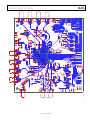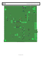
1
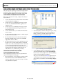
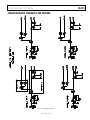
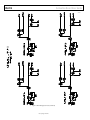
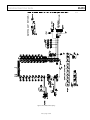
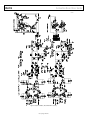
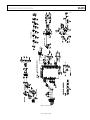
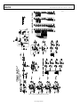
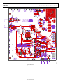
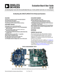
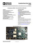
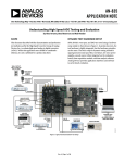
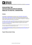
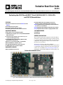
Evaluation Board User Guide
UG-016
One Technology Way • P.O. Box 9106 • Norwood, MA 02062-9106, U.S.A. • Tel: 781.329.4700 • Fax: 781.461.3113 • www.analog.com
Evaluating the AD9276 and AD9277 Octal LNA/VGA/AAF/12-/14-Bit ADCs
and CW I/Q Demodulators
FEATURES
Full featured evaluation board for the AD9276 and the
AD9277
SPI and alternate clock options
Internal and external reference options
VisualAnalog and SPI Controller software interfaces
HSC-ADC-EVALCZ data sheet, High Speed Converter
Evaluation Platform (FPGA-based data capture kit)
AN-905 Application Note, VisualAnalog Converter Evaluation
Tool Version 1.0 User Manual
AN-878 Application Note, High Speed ADC SPI Control Software
AN-877 Application Note, Interface to High Speed ADCs via SPI
EQUIPMENT NEEDED
SOFTWARE NEEDED
Analog signal source and antialiasing filter
2 switching power supplies (6.0 V, 2.5 A) CUI EPS060250UHPHP-SZ, provided
Linear bench top dc voltage source (0 V to 1.6 V), not
required for CW Doppler mode
PC running Windows® 98 (2nd edition), Windows 2000,
Windows ME, or Windows XP
USB 2.0 port, recommended (USB 1.1 compatible)
AD9276 and AD9277 evaluation board
HSC-ADC-EVALCZ FPGA-based data capture kit
For CW Doppler mode: spectrum analyzer
VisualAnalog
SPI Controller
DOCUMENTS NEEDED
AD9276 and AD9277 data sheets
GENERAL DESCRIPTION
This document describes the evaluation board for the AD9276
and AD9277, which provides all of the support circuitry required
to operate the AD9276 and AD9277 in their various modes and
configurations. The application software used to interface with
the devices is also described.
The AD9276 and AD9277 data sheets, available at
www.analog.com, provide additional information and should be
consulted when using the evaluation board. All documents and
software tools are available at http://www.analog.com/fifo. For
any questions, send an email to [email protected].
08282-001
TYPICAL MEASUREMENT SETUP
Figure 1. AD9276-65EBZ/AD9276-80KITZ/AD9277-50EBZ Evaluation Board and HSC-ADC-EVALCZ Data Capture Board
See the last page for an important warning and disclaimers.
Rev. 0 | Page 1 of 28
UG-016
Evaluation Board User Guide
TABLE OF CONTENTS
Features .............................................................................................. 1
Default Operation and Jumper Selection Settings ....................5
Equipment Needed ........................................................................... 1
Evaluation Board Software Quick Start Procedures .....................6
Documents Needed .......................................................................... 1
Configuring the Board For TGC MODE ...................................6
Software Needed ............................................................................... 1
Using the Software for Testing.....................................................6
General Description ......................................................................... 1
Typical Measurement Setup ............................................................ 1
Using the Integrated I/Q Demodulator
(CW Doppler Mode) ....................................................................9
Evaluation Board Hardware ............................................................ 3
Evaluation Board Schematics and Artwork ................................ 11
Power Supplies .............................................................................. 3
Ordering Information .................................................................... 23
Input Signals .................................................................................. 3
Bill of Materials ........................................................................... 23
Output Signals............................................................................... 3
ESD Caution................................................................................ 28
10/09—Revision 0: Initial Version
Rev. 0 | Page 2 of 28
Evaluation Board User Guide
UG-016
EVALUATION BOARD HARDWARE
The evaluation board for the AD9276 and AD9277 provides all of
the support circuitry required to operate the AD9276 and
AD9277 in their various modes and configurations. Figure 2
shows the typical bench characterization setup used to evaluate
the performance of the AD9276 and AD9277. It is critical that
the signal sources used for the analog input and clock have very low
phase noise (<1 ps rms jitter) to realize the optimum performance
of the signal chain. Proper filtering of the analog input signal to
remove harmonics and lower the integrated or broadband noise at
the input is necessary to achieve the specified noise performance
(see the AD9276 or AD9277 data sheet).
See the Evaluation Board Software Quick Start Procedures
section to get started and Figure 21 to Figure 32 for the
complete schematics and layout diagrams that demonstrate the
routing and grounding techniques that should be applied at the
system level.
POWER SUPPLIES
This evaluation board comes with a wall-mountable switching
power supply that provides a 6 V, 2.5 A maximum output. Connect
the supply to the rated 100 V ac to 240 V ac wall outlet at 47 Hz
to 63 Hz. The other end is a 2.1 mm inner diameter jack that
connects to the PCB at P601. Once on the PC board, the 6 V
supply is fused and conditioned before connecting to low dropout
linear regulators that supply the proper bias to each of the various
sections on the board.
When operating the evaluation board in a nondefault condition,
L602, L603, L604, L605, L606, L607, L608, and L609 can be
removed to disconnect the switching power supply. This enables
the user to bias each section of the board individually. Use P602,
P603, and P606 to connect a different supply for each section. At
least one 1.8 V supply is needed with a 1 A current capability for
1.8 V AVDD and 1.8 V DRVDD; however, it is recommended that
separate supplies be used for both analog and digital domains.
An additional supply is also required to supply 3.0 V to the DUT,
3.0 V AVDD2. This should also have a 1 A current capability. To
operate the evaluation board using the SPI and alternate clock
options, a separate 3.3 V analog supply is needed in addition to
the other supplies. The 3.3 V supply, or 3.3 V AVDD, should have a
1 A current capability. To bias the CW I/Q demodulator section
and differential gain drive circuitry, separate +5 V and −5 V
supplies are required at P606. These should each have 1 A current
capability.
INPUT SIGNALS
When connecting the TGC (time gain compensation) ADC
clock, 4LO and analog source, use clean signal generators with
low phase noise, such as Rohde and Schwarz SMA or HP8644B
signal generators or the equivalent. Use a 1 meter shielded, RG-58,
50 Ω coaxial cable for making connections to the evaluation
board. Enter the desired frequency and amplitude (refer to the
specifications in the AD9276 or AD9277 data sheet). In the
default condition, the evaluation board is set up to clock the ADC
from the crystal oscillator, OSC501, when in the TGC mode.
If a different or external ADC clock source is desired, follow the
instructions in the Clock section. Typically, most Analog Devices,
Inc., evaluation boards can accept ~2.8 V p-p or 13 dBm sine
wave input for the clock. When connecting the analog input
source, it is recommended to use a multipole, narrow-band
band-pass filter with 50 Ω terminations. Analog Devices uses
TTE and K&L Microwave, Inc., band-pass filters. The filter
should be connected directly to the evaluation board.
OUTPUT SIGNALS
The default TGC setup uses the FIFO5 high speed, dual-channel
FIFO data capture board (HSC-ADC-EVALCZ). Two of the
eight TGC channels can then be evaluated at the same time. For
more information on channel settings on these boards and their
optional settings, visit http://www.analog.com/fifo.
The default I/Q demodulator setup uses two AD8021 amplifiers
for I-V conversion and two ADA4841 amplifiers for gain and
filtering. The analog outputs can be evaluated using an oscilloscope
or spectrum analyzer.
Rev. 0 | Page 3 of 28
UG-016
Evaluation Board User Guide
WALL OUTLET
100V TO 240V AC
47Hz TO 63Hz
SWITCHING
POWER
SUPPLY
SWITCHING
POWER
SUPPLY
6V DC
2A MAX
SIGNAL
SYNTHESIZER
6V DC
2A MAX
4LO INPUT
ANALOG INPUT
SIGNAL
SYNTHESIZER
PC
RUNNING ADC
ANALYZER
OR VISUAL ANALOG
USER SOFTWARE
AGILENT
POWER SUPPLY
OPTIONAL
CLOCK
INPUT
SPECTRUM
ANALYZER
OSCILLOSCOPE
OR
SIGNAL
SYNTHESIZER
08282-002
GAIN CONTROL
INPUT
CW I/Q
OUTPUTS
Figure 2. Evaluation Board Connection
Rev. 0 | Page 4 of 28
Evaluation Board User Guide
UG-016
DEFAULT OPERATION AND
JUMPER SELECTION SETTINGS
the oscillator from running, and connect the external clock
source to the SMA connector, J503.
This section explains the default and optional settings or modes
allowed on the evaluation board for the AD9276 and AD9277.
A differential LVPECL clock driver can also be used to clock the
ADC input using the AD9516 (U501). Populate C528 and C529
with 0.1 μF capacitors and remove C506 and C507 to disconnect
the default clock path inputs. In addition, populate C511 and C512
with a 0.1 μF capacitor. The AD9516 has many SPI-selectable
options that are set to a default mode of operation. Consult the
AD9516 data sheet for more information about these and other
options.
Power Circuitry
Connect the switching power supply that is supplied in the
evaluation kit between a rated 100 V ac to 240 V ac wall outlet
at 47 Hz to 63 Hz and P601.
Analog Input Front-End Circuit
The evaluation board is set up for single-ended Kelvin
connection analog input with an optimum 50 Ω impedance
match of 18 MHz of bandwidth. For a different bandwidth
response, use the manual tune feature and antialiasing filter
settings.
PDWN
To enable the power-down feature, short P301 (Pin 3 to Pin 4)
to the on position (AVDD) on the PDWN pin.
STBY
VREF
VREF is set to 1.0 V. This causes the ADC to operate with the
internal reference in the 2.0 V p-p full-scale range. A separate
external reference option using the ADR130 is also included on
the evaluation board. Populate R320 with a 0 Ω resistor and remove
C301. Note that ADC full-scale ranges less than 2.0 V p-p are
not supported by the AD9276 and AD9277.
RBIAS
RBIAS has a default setting of 10 kΩ (R304) to ground and is used
to set the ADC core bias current. However, note that using other
than a 10 kΩ, 1% resistor for RBIAS may degrade the performance
of the device, depending on the resistor chosen.
Clock Circuitry
The default clock input circuitry is derived from a simple
transformer-coupled circuit using a high bandwidth 1:1
impedance ratio transformer (T501) that adds a very low amount
of jitter to the clock path. The clock input is 50 Ω terminated
and ac-coupled to handle single-ended sine wave types of inputs.
The transformer converts the single-ended input to a differential
signal that is clipped before entering the ADC clock inputs.
The evaluation board is already set up to be clocked from the
crystal oscillator, OSC501. This oscillator is a low phase noise
oscillator from Valpey Fisher (VFAC3HL-40MHz). If a different
clock source is desired, remove R503, set Jumper J501 to disable
To enable the standby feature, short P301 (Pin 1 to Pin 2) to the
on position (AVDD) on the STBY pin.
GAIN+, GAIN−
To change the VGA attenuation, drive the GAIN+ pin from 0 V
to 1.6 V on J401 using a linear supply. This uses the single-ended
method to change the VGA gain from 0 dB to 42 dB. U411 is
available for users who wish to drive the gain pins (GAIN±)
differentially. Install R426, R435, and R436 and remove C456,
C457, and R440 to connect the amplifier correctly. In differential
mode, a linear supply from −0.8 V to +0.8 V on J401 is required
to change the VGA gain from 0 dB to 42 dB.
If an external source is not available, remove R425, and install
R438 to use the on-board resistive divider (R439) for gain
adjustment in the single-ended case.
CWI/Q+, CWI/Q−
To view the CWI+/CWI− and/or CWQ+/CWQ− outputs,
configure the AD9276 and AD9277 to be in CW mode and
enable each channel via the SPI Controller program. Apply a
13 dBm, 20 MHz reference clock (4LO) on J303. Each enabled
channel is summed and is available through J402/J403.
DOUTx+, DOUTx−
If an alternative data capture method to the setup described in
Figure 2 is used, optional receiver terminations, R604 to R613, can
be installed next to the high-speed backplane connector, P604.
Rev. 0 | Page 5 of 28
UG-016
Evaluation Board User Guide
EVALUATION BOARD SOFTWARE QUICK START PROCEDURES
This section provides quick start procedures for using the AD9276
and AD9277, either on the evaluation board or at the system
level design. Both the default and optional settings are described.
CONFIGURING THE BOARD FOR TGC MODE
Before using the software for testing, configure the evaluation
board as follows:
Connect the evaluation board and the HSC-ADC-EVALCZ
as shown in Figure 1 and Figure 2.
2.
Connect one 6 V, 2.5 A switching power supply (such as
the CUI, Inc., EPS060250UH-PHP-SZ supplied) to the
evaluation board.
3.
Connect one 6 V, 2.5 A switching power supply (such as
the CUI EPS060250UH-PHP-SZ supplied) to the HSCADC-EVALCZ board.
08282-003
1.
Figure 3. VisualAnalog, New Canvas Dialog Box
5.
On the evaluation board, place jumpers on all five pin pairs
of J404 to connect the SPI bus.
6.
On the evaluation board, ensure that J501 (OSC_EN) is
jumpered to the OFF setting to use the on-board 40 MHz
Valpey Fisher VFAC3 oscillator.
7.
On the evaluation board, use a clean signal generator with
low phase noise to provide an input signal to the desired
channel. Use a 1 meter, shielded, RG-58, 50 Ω coaxial cable
to connect the signal generator. For best results, use a
narrow-band band-pass filter with 50 Ω terminations and
an appropriate center frequency (Analog Devices uses
TTE, Allen Avionics, and K&L band-pass filters).
USING THE SOFTWARE FOR TESTING
2.
If a different program is desired, follow Step 3.
Figure 4. VisualAnalog, New Canvas Message Box
3.
Set Up the ADC Data Capture Block
After configuring the evaluation board, set up the ADC data
capture block using the following steps:
1.
After the template is selected, a message box opens, asking
if the default configuration can be used to program the
FPGA (see Figure 4). Click Yes, and the window closes.
08282-004
Connect the USB cable to J6 on the HSC-ADC-EVALCZ
board to the PC.
Open VisualAnalog™ on a PC. AD9276 or AD9277 should
be listed in the status bar of the New Canvas window.
Select the template that corresponds to the type of testing
to be performed (see Figure 3).
To view different channels or change features to settings
other than the default settings, click the Expand Display
button located on the top right corner of the VisualAnalog
window, as shown in Figure 5 and Figure 6.
This process is described in the AN-905 Application Note,
VisualAnalog Converter Evaluation Tool Version 1.0 User
Manual. After you are finished, click the Collapse Display
button.
EXPAND DISPLAY BUTTON
Figure 5. VisualAnalog Window Toolbar, Expand Display Button
Rev. 0 | Page 6 of 28
08282-005
4.
Evaluation Board User Guide
UG-016
Set Up the SPI Controller
After the ADC data capture board setup has been completed,
set up the SPI Controller:
Open the SPI Controller software by going to the Start
menu or double-clicking the SPI Controller software
desktop icon. If prompted for a configuration file, select
the appropriate one. If not, check the title bar at the top of
the SPI Controller window to determine which configuration
is loaded. If necessary, choose Cfg Open from the File
menu and select the appropriate configuration Note that
the CHIP ID(1) field should be filled to indicate whether
the correct SPI Controller configuration file is loaded (see
Figure 8).
08282-006
1.
Figure 6. VisualAnalog, Main Window Expanded Display
Program the FPGA of the HSC-ADC-EVALCZ board to a
setting other than the default setting as described in Step 3.
Then expand the VisualAnalog display and click the Settings
button in the ADC Data Capture block (see Figure 6). The
ADC Data Capture Settings box opens (see Figure 7).
08282-008
4.
Figure 8. SPI Controller, CHIP ID(1) Box
2.
Click the New DUT button in the SPI Controller (see
Figure 9).
08282-007
NEW DUT BUT TON
Figure 7. ADC Data Capture Settings, Board Settings Tab
Select the Board Settings tab and browse to the appropriate
programming file. If you are using an encode rate <28 MSPS,
select Octal_Low_Speed.bin. If you are using an encode
rate >28 MSPS, select Octal_High_Speed.bin. Next, click
Program; the DONE LED in the HSC-ADC-EVALCZ board
should then turn on. If more than two channels are required
to be displayed, select High_Speed_Octal_synchronous_
capture.bin. This canvas allows the user to display all the
channels at once. The drawback is that each FFT display is
only 8k points.
Exit the ADC Data Capture Settings box by clicking OK.
Rev. 0 | Page 7 of 28
08282-009
5.
Figure 9. SPI Controller, New DUT Button
UG-016
In the ADCBase 0 tab of the SPI Controller, find the CHIP
GRADE(2) box. Use the drop-down list box to select the
correct speed mode, if necessary. See the AD9276 or AD9277
data sheet, the AN-878 Application Note, and the AN-877
Application Note for reference.
08282-011
3.
Evaluation Board User Guide
Figure 11. SPI Controller, HIGHPASS(2B)
08282-010
5.
Figure 10. SPI Controller, CHIP GRADE(2)
08282-012
In the ADCBase 0 tab of the SPI Controller, find the
HIGHPASS(2B) box. Click the Manual Tune button to
calibrate the antialiasing filter. See the AD9276 or AD9277
data sheet, the AN-878 Application Note, and the AN-877
Application Note for reference.
Figure 12. SPI Controller, OFFSET(10)
6.
Click the Run button in the VisualAnalog toolbar.
RUN BUTTON
Figure 13. VisualAnalog Window Toolbar, Run Button
Rev. 0 | Page 8 of 28
08282-013
4.
In the Chan A tab of SPI Controller, find the OFFSET(10)
box. Use the drop-down list box labeled Offset Adj to
perform an offset correction to the LNA if the LNA power
setting BIAS_CURR_A(12) is set low. The default value
is 32.
Evaluation Board User Guide
UG-016
Adjust the Amplitude of the Input Signal
3. Click the disk icon within the Graph box to save the
performance plot. See Figure 16.
Next, adjust the amplitude of the input signal for each channel
as follows:
Adjust the amplitude of the input signal so that the
fundamental is at the desired level (examine the Fund
Power reading in the left panel of the VisualAnalog FFT
window). If the gain pin voltage is too low, it is not possible
to reach full scale without distortion. Use a higher gain setting
or a lower input level to avoid distortion. This also depends
on the PGA gain setting, which can be 30 dB, 27 dB, 24 dB
(default), or 21 dB. See Figure 14 and Figure 15.
fIN = 5MHz @ –1dBFS
LNA = 21.6dB
PGA = 24dB
VGAIN = 1.6V
LPF = 1 × 1/3 × FSAMPLE
HPF = FLP ÷ 20.7
–20
AMPLITUDE (dBFS)
1.
0
–40
–60
–80
–100
–140
0
5
10
FREQUENCY (MHz)
15
20
08282-016
–120
Figure 16. Typical FFT, AD9276 and AD9277
USING THE INTEGRATED I/Q DEMODULATOR
(CW DOPPLER MODE)
08282-014
To examine the spectrum of the CW Doppler integrated I/Q
demodulator output, use the following procedure:
1.
Complete the steps in the Configuring the Board and
Using the Software for Testing sections to ensure that the
evaluation board is set up correctly.
2.
Optionally, remove the voltage source from the gain pin,
J401. It does not affect the CW Doppler output.
3.
Use a 1 meter, shielded, RG-58, 50 Ω coaxial cable to
connect the spectrum analyzer to J402 and/or J403.
8.
Connect a 20 MHz signal source to J303, 4LO input. Use a
clean signal generator with low phase noise to provide an
input clock signal. Use a 1 meter, shielded, RG-58, 50 Ω
coaxial cable to connect the signal generator.
9.
Connect an analog input signal, 5.0123 MHz for example,
to ChA, J101. Use a clean signal generator with low phase
noise to provide an input signal to the desired channel. Use
a 1 meter, shielded, RG-58, 50 Ω coaxial cable to connect
the signal generator. For best results, use a narrow-band
band-pass filter with 50 Ω terminations and an appropriate
center frequency (Analog Devices uses TTE, Allen
Avionics, and K&L band-pass filters).
4.
In the ADCBase 0 tab of the SPI Controller, find the
MODES(8) box. Select the CW Mode option (see Figure 17).
08282-015
Figure 14. VisualAnalog, FFT Graph, Gain = 0 V
Figure 15. VisualAnalog, FFT Graph, Gain = 1.6 V
2.
If another channel needs to be evaluated, change the
channel setting within the ADC Data Capture block.
Channels A and B are the default displayed channels ADC
Data Capture Settings box under the General tab. Clock
Frequency and the number of samples can also be changed.
Rev. 0 | Page 9 of 28
UG-016
Evaluation Board User Guide
6.
An example of the CW Doppler output, as shown in Figure 19
and Figure 20, can be seen in the frequency and time domain,
respectively. Make sure to set the analog input level appropriately to achieve full scale throughout the signal chain.
REF Lv1
0dBm
MARKER 1 [T1]
–1.91dBm
13.38605210kHz
0
RBW 100Hz RF ATT 30dB
VBW 100Hz
dBm
1 SWT 12.5s UNIT
A
–10
–20
–30
–40
1AVG
1SA
–50
–60
–70
–80
–90
–110
–120
START 20Hz
2.498kHz
STOP 25kHz
08282-032
–100
Figure 19. Typical Spectrum Analyzer Display of CWD Output
TEK RUN: 2.50MS/s
SAMPLE
]
08282-017
[ T
C3 FREQ
12.330kHz
UNSTABLE
HISTOGRAM
Figure 17. SPI Controller, MODES(8) Box
In the Chan X tab of the SPI Controller, where X is the
channel to which an analog input is applied, find the
CW_IQ_DEMOD_PH(2D) box. Select the CW Channel
Enabl check box to enable the channel. Then select the
phase rotation of the channel using the I/Q Demoduator
Phase drop-down menu.
C3 p-p
576mV
T
CH3 100mVΩ
M20.0µs
CH3
8mV
Figure 20. Typical Oscilloscope Display of CWD Output
Figure 18. SPI Controller, CW_IQ_DEMOD_PH(2D) Box
Rev. 0 | Page 10 of 28
08282-033
3
08282-018
5.
Evaluation Board User Guide
UG-016
EVALUATION BOARD SCHEMATICS AND ARTWORK
08282-020
Figure 21. DUT Analog Input Circuits
Rev. 0 | Page 11 of 28
UG-016
Evaluation Board User Guide
08282-021
Figure 22. DUT Analog Input Circuits (Continued)
Rev. 0 | Page 12 of 28
Evaluation Board User Guide
UG-016
08282-022
Figure 23. DUT, VREF, and Decoupling
Rev. 0 | Page 13 of 28
UG-016
Evaluation Board User Guide
08282-023
Figure 24. I/Q Demodulator, SPI, and Gain Drive Circuitry
Rev. 0 | Page 14 of 28
Evaluation Board User Guide
UG-016
08282-024
Figure 25. Clock Circuitry
Rev. 0 | Page 15 of 28
UG-016
Evaluation Board User Guide
08282-025
Figure 26. Power Supply, Digital Output Interface
Rev. 0 | Page 16 of 28
UG-016
08282-026
Evaluation Board User Guide
Figure 27. Top Side
Rev. 0 | Page 17 of 28
Evaluation Board User Guide
08282-027
UG-016
Figure 28. Ground Plane (Layer 2)
Rev. 0 | Page 18 of 28
UG-016
08282-028
Evaluation Board User Guide
Figure 29. Power Plane (Layer 3)
Rev. 0 | Page 19 of 28
Evaluation Board User Guide
08282-029
UG-016
Figure 30. Power Plane (Layer 4)
Rev. 0 | Page 20 of 28
UG-016
08282-030
Evaluation Board User Guide
Figure 31. Ground Plane (Layer 5)
Rev. 0 | Page 21 of 28
Evaluation Board User Guide
08282-031
UG-016
Figure 32. Bottom Side
Rev. 0 | Page 22 of 28
Evaluation Board User Guide
UG-016
ORDERING INFORMATION
BILL OF MATERIALS
Table 1.
Qty
103
4
Reference Designator
C101, C102, C106, C110, C111, C115, C120, C121, C125, C130, C131,
C136, C201, C202, C206, C210, C211, C215, C220, C221, C225, C230,
C231, C236, C302, C303, C304, C307, C308, C309, C310, C311, C312,
C313, C314, C315, C316, C317, C318, C319, C320, C326, C327, C328,
C329, C330, C404, C413, C415, C418, C419, C420, C421, C422, C423,
C424, C431, C437, C439, C442, C443, C444, C445, C446, C447, C448,
C450, C451, C453, C454, C455, C456, C457, C458, C459, C462, C463,
C501, C502, C503, C504, C505, C506, C507, C510, C518, C519, C520,
C521, C522, C523, C527, C530, C531, C532, C533, C534, C615, C617,
C619, C621, C627, C629
C624, C625, C634, C635
1
C509
1
C636
2
C449, C452
5
C401, C407, C425, C430, C630
6
C408, C409, C410, C432, C433, C434
4
C411, C412, C435, C436
1
C515
1
C631
4
C403, C405, C427, C428
4
C603, C606, C609, C612
1
C516
1
C301
10
C602, C604, C605, C607, C608, C610, C611, C613, C622, C623
10
C414, C416, C438, C440, C614, C616, C618, C620, C626, C628
1
C632
1
C633
6
C402, C406, C426, C429, C460, C461
1
C601
5
10
CR301, CR302, CR303, CR304, CR601
D101, D102, D103, D104, D201, D202, D203, D204, D301, D501
5
D601, D602, D603, D604, D605
1
D606
1
1
D607
F601
Description
Capacitor, 0.1 μF, 0402,
X5R, ceramic, 10 V
Manufacturer
Panasonic
Part Number
ECJ-0EB1A104K
Capacitor, 1 μF, 0402,
6.3 V, ceramic, X5R
Capacitor, 0.22 μF, 0402,
6.3 V, ceramic
Capacitor, 100 pF, 0402,
50 V, Ceramic
Capacitor, 1000 pF, 0402,
50 V, ceramic, X7R
Capacitor, 1500 pF, 0402,
25 V, ceramic, X7R
Capacitor, 150 pF, 0402,
25 V, ceramic, X7R
Capacitor, 2700 pF, 0402,
25 V, ceramic, X7R
Capacitor, 3900 pF, 0402,
25 V ceramic, X7R
Capacitor, 33 pF, 0402,
25 V ceramic, X7R
Capacitor, 5 pF, 0603, 50 V,
ceramic, NPO
Capacitor, 10000 pF,
0402, 16 V, ceramic, X7R
Capacitor, 22000 pF,
0402, 25 V, ceramic, Y5V
Capacitor, 1 μF, 0603,
16 V, ceramic, X5R
Capacitor, 4.7 μF, 0603,
6.3 V, ceramic, X5R
Capacitor, 10 μF, 0603,
6.3 V, ceramic, X5R
Capacitor, 4.7 μF, 0805,
6.3 V, ceramic X5R
Capacitor, 47 μF, 0805,
6.3 V, Ceramic, X5R
Capacitor, 22 μF, 0805,
6.3 V, ceramic, X5R
Capacitor, 10 μF, 6032-28,
tantalum, SMT, 16 V, 10%
LED, 0603, green
Diode Schottky GP LN
20 V SOT-23 200 mA SS
Diode, silicon rectifier,
SMBJ, 2 A, 50 V
MOSFET P-CH 30 V 3.1 A
SOT-23
Diode, Schottky, 2 A, 20 V
Polyswitch 1.10 A reset
fuse SMD
Panasonic
ECJ-0EB0J105M
Panasonic
ECJ-0EB0J224K
Murata
GRM1555C1H101JD01B
Panasonic
ECJ-0EB1H102K
Panasonic
ECJ-0EB1E152K
Panasonic
ECJ-0EB1H151K
Panasonic
ECJ-0EB1E272K
Panasonic
ECJ-0EB1E392K
Panasonic
ECJ-0EC1H330J
Yageo
CC0603CRNP09BN5R0
Panasonic
ECJ-0EB1C103K
Panasonic
ECJ-0EF1E223Z
Panasonic
ECJ-BVB1C105M
Panasonic
ECJ-1VB0J475M
Panasonic
ECJ-1VB0J106M
Murata
GRM21BR61E475KA12L
Taiyo Yuden
JMK212BJ476MG-T
Panasonic
ECJ-2FB0J226M
Kemet
T491C106K016AT
Panasonic
Fairchild
LNJ314G8TRA
MMBD4148SE
Microcommerical
S2A-TP
Vishay
SI2343DS-TI-E3
Diodes Inc
Tyco/Raychem
DFLS220L-7
NANOSMDC110F-2
Rev. 0 | Page 23 of 28
UG-016
Qty
15
Evaluation Board User Guide
1
Reference Designator
J101, J102, J103, J104, J201, J202, J203, J204, J401, J402, J403, J303,
J503, J504, J505
J305
1
J404
1
J501
1
J502
2
J301, TP501
1
J304
1
2
3
14
1
P601
P604, P605
P602, P603, P606
L401, L402, L602, L603, L604, L605, L606, L607, L608, L609, L610, L611,
L612, L613
L601
1
L614
1
OSC501
15
8
R101, R115, R130, R145, R201, R215, R230, R245, R319, R425, R498,
R499, R504, R531, R532
R102, R116, R131, R146, R202 R216, R231, R246, R503, R505, R506,
R507, R508, R509, R510, R511, R519, R526, R527, R451, R453, R455,
R456, R457, R458, R460, R462, R535
R107, R121, R136, R151, R207, R221, R236, R251
10
R301, R302, R305, R441, R442, R443, R405, R417, R449, R450
20
6
R303, R304, R306, R403, R415, R444, R445, R446, R466, R467, R501,
R502, R514, R515, R516, R538, R539, R602, R615
R407, R409, R410, R419, R421, R422
6
R307, R308, R309, R310, R321, R517
5
R427, R429, R520, R521, R528
2
R428, R430
3
R440, R522, R523
2
R431, R432
2
R534, R536
4
R401, R404, R413, R416
1
R447
1
R433
1
R434
1
R437
1
R439
1
R518
28
Description
SMA, end launch, coax
Manufacturer
Samtec
Part Number
SMA-J-P-H-ST-EM1
Header, 4 pin double row,
male, 100 mil, straight
Header, 5 pin double row,
male, 100 mil, straight
Header, 3 pin single row,
male, 100 mil, straight
Header, 3 pin double row,
male, 100 mil, straight
Header, 2 pin double row,
male, 100 mil, straight
Header, 2 pin single row,
male, 100 mil, straight
Power supply connector
Connector, 60 pin RA
Terminal block, 4-pin, ST
Inductor, ferrite bead,
50 Ω 3 A 1206
EMI filter LC block choke
coil
Inductor, 4.7 μH,
shielded power
Clock oscillator, ACMOS/
LSTTL compatible
Resistor, 49.9 Ω, 0402,
1/16 W, 1%
Resistor, 0 Ω, 0402,
1/16 W, 1%
Samtec
TSW-104-07-G-D
Samtec
TSW-105-07-G-D
Samtec
TSW-103-07-G-S
Samtec
TSW-103-07-G-D
Samtec
TSW-102-07-G-D
Samtec
TSW-102-07-G-S
Switchcraft
Tyco
Weiland
Muarata
RAPC722X
6469169-1
Z5.531.3425.0
BLM31PG500SN1L
Murata
BNX016-01
Coilcraft
LPS5015-472MLB
Valpey Fisher
VFAC3H-L-40MHz
Panasonic
ERJ-2RKF49R9X
Panasonic
ERJ-2GE0R00X
Panasonic
ERJ-2RKF3480X
Panasonic
ERJ-2RKF1001X
Panasonic
ERJ-2RKF1002X
Panasonic
ERJ-2GEJ203X
Panasonic
ERJ-2GEJ512X
Panasonic
ERJ-2RKF2000X
Panasonic
ERJ-2RKF2210X
Panasonic
ERJ-2GEJ101X
Panasonic
ERJ-2RKF24R0X
Panasonic
ERJ-2RKF24R9X
Panasonic
ERJ-2RKF2001X
Panasonic
ERJ-2RKF27R0X
Panasonic
ERJ-2GEJ333X
Panasonic
ERJ-2RKF1052X
Panasonic
ERJ-2RKF8661X
Copal
CT94EW103
Panasonic
ERJ-2RKF4121X
Resistor, 348 Ω, 0402,
1/16 W, 1%
Resistor, 1.00 kΩ, 0402,
1/16 W, 1%
Resistor, 10.0 kΩ, 0402,
1/16 W, 1%
Resistor, 20.0 kΩ, 0402,
1/16 W, 5%
Resistor, 5.1 kΩ, 0402,
1/16 W, 5%
Resistor, 200 Ω, 0402,
1/16 W, 1%
Resistor, 221 Ω, 0402,
1/16 W, 1%
Resistor, 100 Ω, 0402,
1/16 W, 1%
Resistor, 24 Ω, 0402,
1/16 W, 1%
Resistor, 24.9 Ω, 0402,
1/16 W, 1%
Resistor, 2.00 kΩ, 0402,
1/16 W, 1%
Resistor, 27 Ω, 0402,
1/16 W, 1%
Resistor, 33 kΩ, 0402,
1/16 W, 5%
Resistor, 10.5 kΩ, 0402,
1/16 W, 1%
Resistor, 8.66 kΩ, 0402,
1/16 W, 1%
Potentiometer, 10 kΩ sq
cermet top
Resistor, 4.12 kΩ, 0402,
1/16 W, 1%
Rev. 0 | Page 24 of 28
Evaluation Board User Guide
UG-016
Qty
3
Reference Designator
R540, R541, R601
1
R603
1
1
R614
R616
1
12
R617
L403, L404, L405, L406, L407, L408, L409, L410, L411, L412, L413, L414
2
2
T301, T501
U403, U408
1
U304
4
U401, U402, U406, U407
2
U404, U409
2
U405, U410
1
U411
1
U501
1
U601
1
U602
2
U603, U604
1
U605
1
U608
1
U412
1
U413
1
U606
1
U607
1
U302
1
10
U301
MP101, MP102, MP103, MP104, MP105, MP106, MP107, MP108,
MP109, MP110
4
MP111, MP112, MP113, MP114
20
3
Description
Resistor, 249 Ω, 0402,
1/16 W, 1%
Resistor, 1.91 kΩ, 0402,
1/16 W, 1%
Resistor, 64.9 kΩ, 0402
Resistor, 0.047 Ω, 0805,
1/4 W, 2%
Resistor, 16.9 kΩ, 0402
Resistor, 0 Ω, 0603
1/10 W, 5%
Transformer, RF, 1:1
IC, amp, low PWR, noise,
distortion, SO8
IC, voltage REF, precision
series, SOT23_6
IC, amp, low noise high
speed, SO8
IC, ADC, 18-bit, 1 MSPS
PuLSAR 7.0 mW, RM10
IC, VREF, prec micropwr,
low dropout, SO8
IC, ADC driver, ultra-low
distortion diff, LFCSP16
IC, clock gen, 14-output,
2.8 GHZ VCO, QFN64
IC, regulator 3.3 V, low
dropout CMOS, SO8
IC, regulator 3.0 V, low
dropout CMOS, SO8
IC, regulator 1.8 V, low
dropout CMOS, SO8
IC, regulator 0.8 V to
5.0 V, low dropout
CMOS, SO8
IC-ADI high ACC. 500 mA
anycap low drop 2.5 V reg
IC, buffer, tinylogic UHS
dual, SC70
IC, buffer, tinylogic UHS
dual, SC70
IC, regulator, 500 mA
neg LDO
IC-ADI current-mode
step-down dc-to-dc
controller
IC-ADI ultrafast SIGe ECL
clock/data buffers
IC
Part of assembly
Part of assembly
Do Not Install
C305, C306, C511, C512, C513, C514, C528, C529, C464, C465, C466,
C467, C468, C469, C470, C471, C472, C473, C474, C475
C524, C525, C526
Capacitor, 0.1 μF, 0402,
X5R, ceramic, 10 V
Capacitor, 100 pF, 0402,
50 V, ceramic, X7R
Rev. 0 | Page 25 of 28
Manufacturer
Panasonic
Part Number
ERJ-2RKF2490X
Panasonic
ERJ-2RKF1911X
Panasonic
Susumu
ERJ-2RKF6492X
RL1220T-R047
Panasonic
Panasonic
ERJ-2RKF1692X
ERJ-3GEY0R00V
Minicircuits
ADI
ADT1-1WT+
ADA4841-2YRZ
ADI
ADR130BUJZ
ADI
AD8021ARZ
ADI
AD7982BRMZ
ADI
ADR434ARZ
ADI
ADA4938-1ACPZ-R7
ADI
AD9516-0BCPZ
ADI
ADP1706ARDZ-3.3-R7
ADI
ADP1706ARDZ-3.0-R7
ADI
ADP1706ARDZ-1.8-R7
ADI
ADP1708ARDZ-R7
ADI
ADP3335ACPZ-2.5R7
FAIRCHILD
NC7WZ07P6X
FAIRCHILD
NC7WZ16P6X
Linear
Technology
ADI
LT1175CST-5#PBF
ADP1864AUJZ-R7
ADI
ADCLK905
ADI
Place into J404
(Pin 1-2, 3-4, 5-6,
7-8,9-10), J301
(Pin 1-2, 3-4), J304
(Pin 1-2), J502
(Pins 3-4), J501
(Pins 2-3)
Insert/Snap into
the large holes
from the bottom
side of board
AD9276BSVZ
100 mil jumpers
Panasonic
ECJ-0EB1A104K
Panasonic
ECJ-0EB1H101K
14 mm height, dual
locking standoffs for
circuit board support
UG-016
Evaluation Board User Guide
Qty
8
Reference Designator
C105, C114, C124, C135, C205, C214, C224, C235
2
C417, C441
3
L501, L502, L503
12
2
R106, R120, R135, R150, R213, R220, R235, R250, R408, R420, R452,
R454
R402, R414
9
R320, R426, R435, R436, R438, R464, R465, R533, R537
13
2
R604, R605, R606, R607, R608, R609, R610, R611, R612, R613, R329,
R459, R463
R406, R418
1
R513
4
R411, R412, R423, R424
4
TP1, TP2, TP3, TP4
Description
Capacitor, 47 pF, 0402,
X5R, ceramic, 50 V
Capacitor, 1 μF, 0805,
16 V, ceramic, Y5V
Inductor, 10 nH, SMT
L7144
Resistor, 1.00 kΩ, 0402,
1/16 W, 1%
Resistor, 10.0 kΩ, 0402,
1/16 W, 1%
Resistor, 0 Ω, 0402,
1/16 W, 1%
Resistor, 100 Ω, 0402,
1/16 W, 1%
Resistor, 10.0 kΩ, 0402,
1/16 W, 1%
Resistor, 49.9 Ω, 0402,
1/16 W, 1%
Resistor, 20 Ω, 0402,
1/16 W, 1%
Conn-PCB test point, blk
Rev. 0 | Page 26 of 28
Manufacturer
Panasonic
Part Number
ECJ-0EC1H470J
Panasonic
ECJ-2VF1C105Z
Coilcraft
0603CS-10NXJLW
Panasonic
ERJ-2RKF1001X
Panasonic
ERJ-2RKF1002X
Panasonic
ERJ-2GE0R00X
Panasonic
ERJ-2GEJ101X
Panasonic
ERJ-2RKF20R0X
Keystone
Electronics Corp
5001
Evaluation Board User Guide
UG-016
NOTES
Rev. 0 | Page 27 of 28
UG-016
Evaluation Board User Guide
NOTES
ESD CAUTION
Evaluation boards are only intended for device evaluation and not for production purposes. Evaluation boards are supplied “as is” and without warranties of any kind, express,
implied, or statutory including, but not limited to, any implied warranty of merchantability or fitness for a particular purpose. No license is granted by implication or otherwise under
any patents or other intellectual property by application or use of evaluation boards. Information furnished by Analog Devices is believed to be accurate and reliable. However, no
responsibility is assumed by Analog Devices for its use, nor for any infringements of patents or other rights of third parties that may result from its use. Analog Devices reserves the
right to change devices or specifications at any time without notice. Trademarks and registered trademarks are the property of their respective owners. Evaluation boards are not
authorized to be used in life support devices or systems.
©2009 Analog Devices, Inc. All rights reserved. Trademarks and
registered trademarks are the property of their respective owners.
UG08282-0-10/09(0)
Rev. 0 | Page 28 of 28