1
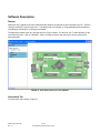
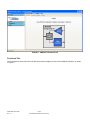
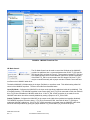
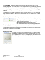
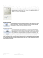
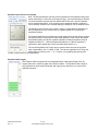
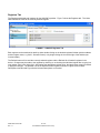
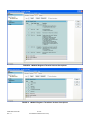
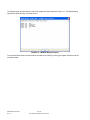
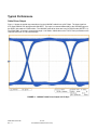
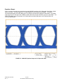
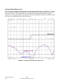
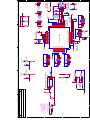
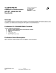
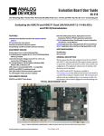
SD387EVK
National Semiconductor
EVK User Manual
LMH0387 Evaluation Board
User Guide
April 29, 2010
Overview
The SD387 Evaluation Kit (EVK) enables evaluation of the LMH0387 3G/HD/SD SDI Configurable I/O Adaptive
Cable Equalizer / Cable Driver. A graphical user interface allows managing the SPI registers for the input mode
(equalizer), and can also be used to control the device’s I/O mode.
Evaluation Kit (SD387EVK) Contents
The EVK contains the following parts:
• SD387EVK board assembly with the LMH0387 configurable I/O
• SPA dongle (SPIÆUSB card)
• USB cable
• 6-pin parallel cable
• SD387EVK User Guide
Evaluation Board Description
Figure 1 shows the SD387 evaluation board and highlights some of its features.
SD387EVK User Guide
Rev 1.1
1 of 23
© 2010 National Semiconductor Corp.
FIGURE 1. SD387 Evaluation Board
Inputs and Outputs: BNC_IO Input/Output, SDI Input, and SDO Output
The bidirectional I/O (J1) is a 75Ω BNC connector. When the LMH0387 is configured as an input, the input signal
on the BNC_IO pin should conform to the SMPTE 424M, SMPTE 292M, or SMPTE 259M standards. When the
LMH0387 is configured as an output, the BNC_IO pin will drive SMPTE SDI signal levels (800 mVP-P into 75Ω).
The SDI input connectors (J2 and J3) are 50Ω SMA connectors. This cable driver input includes a 100Ω differential
termination resistor (R5) at the LMH0387 device and is optimized for 100Ω differential input.
The SDO output connectors (J4 and J5) are 50Ω SMA connectors. When using only one side of this equalizer
output pair, the other side should be terminated with a 50Ω SMA termination. For example, when only using the
SDO output, ¯¯¯¯
SDO should be terminated with a 50Ω SMA termination.
SD387EVK User Guide
Rev 1.1
2 of 23
© 2010 National Semiconductor Corp.
DC Power Connectors
The VCC and GND power connectors should be powered with a DC input voltage of 3.3V ± 5% (3.6V maximum).
JP2 Controls
¯¯¯
CD
JP2 allows monitoring of the Carrier Detect (¯¯¯
CD ) at the BNC_IO pin while in the input mode (equalizer). ¯¯¯
CD is
asserted low when an input signal is detected at the BNC_IO pin, and high when no input signal is present.
TX_EN
JP2 allows control of the TX_EN pin to enable or disable the cable driver. The LMH0387 TX_EN pin has an
internal pullup to enable the cable driver by default, so this pin may be left unconnected when using the LMH0387
in the output mode. To disable the cable driver, place a jumper to tie TX_EN to GND. When using the LMH0387 in
the input mode, the cable driver must be disabled by tying TX_EN low. TX_EN may optionally be controlled via the
GUI using the SPA dongle as described below.
¯¯¯
SD/HD
JP2 allows control of the SD/¯¯¯
HD pin for setting the slew rate for the BNC_IO pin while the LMH0387 is in the output
mode (cable driver). This pin may be connected to GND for the faster HD/3G slew rate or connected to VCC for the
¯¯¯ pin has an internal pulldown to enable the HD/3G slew rate by default.
slower SD slew rate. The LMH0387 SD/HD
SPI Header (JP1)
JP1 is the SPI (Serial Peripheral Interface) header. It allows access to the SPI pins (¯¯¯
SS , MISO, MOSI, and SCK)
to control the SPI registers of the LMH0387 equalizer. To use the SPI interactive GUI, plug the 6-pin parallel cable
between this header and JP7 on the SPA dongle to connect the pins one-for-one as shown in Table 1. The SPA
dongle requires special software and must be connected to the PC via the USB – see the Software Setup section.
TABLE 1. SPI Connections between SD387 and SPA Dongle
SD387 JP1
Pin #
Name
1
GND
2
SCK
3
MOSI
4
MISO
5
SS
6
GND
Æ
Æ
Æ
Æ
Æ
Æ
SPA Dongle JP7
Pin #
Name
1
GND
2
MCK
3
MOSI
4
MOSI
5
SS
6
GND
Carrier Detect LED (D1)
D1 shows the status of Carrier Detect at the LMH0387 equalizer input. This LED is GREEN when an input signal
has been detected at the BNC_IO pin, and OFF when no input is detected.
SD387EVK User Guide
Rev 1.1
3 of 23
© 2010 National Semiconductor Corp.
SPA Dongle Description
The SPA dongle is required to use the SPI interactive GUI. The SPA dongle connects between the LMH0387 SPI
pins and the USB input of a PC. The SPA dongle is shown in Figure 2. JP7 is the SPI Header. The SPA dongle is
powered through the USB, and the D1 LED is RED when the SPA dongle is connected to a PC via the USB to
indicate the board is powered.
FIGURE 2. SPA Dongle
Figure 3 shows the connection between the SD387 and the SPA dongle. For proper operation, the SPI pins must
be connected between the SD387 JP1 and the SPA dongle JP7. Optionally, a single wire may be connected
between the SD387 TX_EN pin (JP2) and the SPA dongle PA0 (J7) to enable software control of the LMH0387
cable driver enable functionality, and allow the GUI to fully control the LMH0387 I/O Mode as described on page 8.
If this connection is not used, then the TX_EN can be controlled manually with a jumper.
FIGURE 3. SD387 Connection to SPA Dongle
SD387EVK User Guide
Rev 1.1
4 of 23
© 2010 National Semiconductor Corp.
Software Setup
System Requirements
Operating System:
USB:
Windows XP or Vista
2.0
Installation
Download the latest software from the LMH0387 Evaluation Board page. Extract the ALPF_monthdayyear_major
version_minor version.exe” (ex. ALPF_04062010_128_0002.exe) file to a temporary location that can be deleted
later.
Make sure the SPA dongle is not connected to the PC. The following installation instructions are for the Windows
XP Operating System.
Install the ALP software
Execute the ALP Setup Wizard program called “ALPF_monthdayyear_major version_minor version.exe” (ex.
ALPF_04062010_128_0002.exe) that was extracted to a temporary location.
There are 7 steps to the installation once the setup wizard is started:
1. Select the “Next” button.
2. Select “I accept the agreement” and then select the “Next” button.
3. Select the location to install the ALP software and then select the “Next” button.
4. Select the location for the start menu shortcut and then select the “Next” button.
5. There will then be a screen that allows the creation of a desktop and Quick Launch icon. After selecting
the desired choices select the “Next” button.
6. Select the “Install” button, and the software will then be installed to the selected location.
7. Uncheck “Launch Analog LaunchPAD” and select the “Finish” button. The ALP software will start if
“Launch Analog LaunchPAD” is checked, but it will not be useful until the USB driver is installed.
Connect JP1 of the SD387 evaluation board to JP7 of the SPA dongle via the 6-pin parallel cable as shown in
Table 1. Power on the SD387 evaluation board with a 3.3 VDC power supply. Connect the SPA dongle to the PC
with the USB cable. The “Found New Hardware Wizard” will open on the PC. Proceed to the next section to install
the USB driver.
Install the USB driver
There are 6 steps to install the USB driver:
1. Select “No, not at this time” then select the “Next” button.
2. Select “Install from a list or specific location” then select the “Next” button.
3. Select “Search for the best driver in these locations”. Uncheck “Search removable media” and check
“Include this location in the search”.
4. Browse to the Install Directory which is typically located at “C:\Program Files\National Semiconductor
Corp\Analog LaunchPAD\vx.x.x\Drivers” and select the “Next” button. Windows should find the driver.
5. Select “Continue Anyway”.
6. Select the “Finish” button.
The software installation is complete. The ALP software may now be launched, as described in the next section.
SD387EVK User Guide
Rev 1.1
5 of 23
© 2010 National Semiconductor Corp.
Software Description
Startup
Make sure all the software has been installed and the hardware is powered on and connected to the PC. Execute
“Analog LaunchPAD” from the start menu. The default start menu location is “Programs\National Semiconductor
Corp\Analog LaunchPAD vx.x.x\Analog LaunchPAD”.
The application should come up in the state shown in Figure 4 below. If it does not, see “Trouble Shooting” at the
end of this document. Click on “LMH0387 – Nano” to select the device and open up the device profile and its
associated tabs.
FIGURE 4. ALP Startup Screen for the LMH0387
Information Tab
The Information tab is shown in Figure 5.
SD387EVK User Guide
Rev 1.1
6 of 23
© 2010 National Semiconductor Corp.
FIGURE 5. LMH0387 Information Tab
Functional Tab
The Functional tab is the main tab of the GUI and presents a high level view of the LMH0387 equalizer, as shown
in Figure 6.
SD387EVK User Guide
Rev 1.1
7 of 23
© 2010 National Semiconductor Corp.
FIGURE 6. LMH0387 Functional Tab
I/O Mode Control
The I/O Mode Control can be used to control the I/O Mode of the LMH0387,
provided an additional wire is connected between the SD387 TX_EN and the
SPA dongle PA0, as shown in Figure 3. The connection between TX_EN and
PA0 allows software control of the LMH0387 cable driver enable functionality.
If the SD387 TX_EN is not connected to the SPA dongle PA0, then TX_EN
may be controlled manually with a jumper and the I/O Mode Control will have
no effect on the LMH0387 cable driver.
The default LMH0387 I/O Mode setting is the Input (Rx) Mode, or equalizer mode. This default setting allows full
control of the LMH0387 equalizer. The three I/O modes are described below.
Input (Rx) Mode: Configures the LMH0387 for the input mode (equalizer enabled and cable driver disabled). This
is the default setting. The LMH0387 equalizer is set to auto sleep, and if TX_EN is connected to PA0, then PA0 will
drive TX_EN low to disable the LMH0387 cable driver. If this TX_EN Æ PA0 connection is not made, then the
LMH0387 cable driver should be manually disabled by setting a jumper to tie TX_EN to GND.
Output (Tx) Mode: Configures the LMH0387 for the output mode (cable driver enabled and equalizer disabled).
The LMH0387 equalizer is forced to sleep. If TX_EN is connected to PA0, then PA0 will drive TX_EN high to
enable the LMH0387 cable driver. If this TX_EN Æ PA0 connection is not made, then the LMH0387 cable driver
should be manually enabled by pulling the jumper between TX_EN and GND (TX_EN should be open).
SD387EVK User Guide
Rev 1.1
8 of 23
© 2010 National Semiconductor Corp.
Tx Loopback Mode: Configures the LMH0387 for the output mode with a loopback path (cable driver and
equalizer both enabled). The LMH0387 equalizer is set to auto sleep. If TX_EN is connected to PA0, then PA0 will
drive TX_EN high to enable the LMH0387 cable driver. If this TX_EN Æ PA0 connection is not made, then the
LMH0387 cable driver should be manually enabled by pulling the jumper between TX_EN and GND (TX_EN should
be open). In this mode, the cable driver output on the BNC_IO pin is looped back to the LMH0387 equalizer
¯¯¯¯
outputs (SDO and ¯¯¯¯
SDO ), so the cable driver output may be observed both at BNC_IO pin and at the SDO/SDO
output pins.
The Cable Driver TX_EN indicator shows the current status of the TX_EN control (only if TX_EN is connected to
PA0). It is GREEN to indicate TX_EN is driven high and the LMH0387 cable driver is enabled, or OFF to indicate
TX_EN is driven low and the LMH0387 cable driver is disabled.
Equalizer Sleep Mode and Carrier Detect
The Equalizer Sleep Mode control shows the status of the Sleep Mode
register bits and allows control over the sleep mode. The Equalizer Sleep
Mode settings are as follows:
On: Force the equalizer into sleep mode (powered down) regardless of
whether there is an input signal or not.
Off: Disable sleep mode (force equalizer to stay enabled).
Auto: Sleep mode active when no input signal detected (default mode).
The Equalizer Sleep Status indicator shows the current sleep status of the equalizer. It is GREEN to indicate
sleeping or OFF to indicate not sleeping.
The Carrier Detect shows the status of the BNC_IO input carrier detect. It is GREEN to indicate the input signal is
present or OFF to indicate the input signal is absent.
Equalizer Output Swing
The Equalizer Output Swing control shows the current value of the LMH0387 equalizer
output amplitude and allows adjustment in 100 mV increments from 400 mVP-P to 800
mVP-P. The default setting is 700 mVP-P. The Equalizer Output Swing may be set either
by clicking on the “+” or “-” buttons, or by grabbing and spinning the “handle” on the
knob for a quick adjustment.
SD387EVK User Guide
Rev 1.1
9 of 23
© 2010 National Semiconductor Corp.
Equalizer Output Offset
The Equalizer Output Offset control shows the current value of the LMH0387 equalizer
output common mode voltage and allows adjustment in 200 mV increments from 1.05V
to 1.85V. At the “Max” setting, the outputs are referenced to the positive supply and the
output common mode is 2.1V. The default setting is 1.25V. The Equalizer Output Offset
may be set either by clicking on the “+” or “-” buttons, or by grabbing and spinning the
“handle” on the knob for a quick adjustment.
Equalizer Output Mute
The Equalizer Output Mute indicator shows the mute status, and the button may be used to
toggle the mute function. The indicator is GREEN to indicate mute (equalizer outputs are
muted) and OFF to indicate normal mode (outputs are not muted).
Extended 3G Reach Mode
The Extended 3G Reach Mode indicator shows the status of the Extended 3G Reach
Mode register bit, and the button may be used to toggle this register bit. The indicator is
GREEN when the bit is set for extended 3G reach mode, and OFF when the equalizer is
set for normal mode. Note that the indicator shows the status of the register bit – not
whether the device is actually in extended 3G reach mode or not. If extended 3G reach
mode is set, the equalizer will remain in this mode until the input cable is physically
changed or power is cycled. For example, extended 3G reach mode is forced, and then it is turned off. The
indicator will show it is off, but the equalizer will still be in extended 3G reach mode until the input cable is changed
or the device power is cycled. The GUI provides a simple way to reset the extended 3G reach mode: the Extended
3G Reach Mode Reset button. This button toggles the equalizer sleep mode, and has a similar effect to removing
and re-applying the input cable.
SD387EVK User Guide
Rev 1.1
10 of 23
© 2010 National Semiconductor Corp.
Equalizer Input Launch Level Control
Note: The GUI automatically sets the nominal equalizer launch amplitude setting upon
startup (specifically, it writes 30h to SPI register 02h). This nominal setting is required
for correct equalizer operation with the default SMPTE 800 mVP-P launch amplitude
and no external attenuation. If the equalizer launch amplitude setting is changed, it
can be instantly set back to this nominal setting by clicking the “Set To Default” button.
The Equalizer Input Launch Level Control is useful to compensate for attenuation of
the input signal prior to the equalizer due to a passive splitter or non-ideal input
termination network.
The Coarse Amplitude control shows the current setting of the Coarse Control register
and may be used to set the input for either 0 dB (default) or 6 dB of input attenuation.
At the default setting of 0 dB, the equalizer operates normally and expects a launch
amplitude of 800 mVP-P. With the Coarse Amplitude set to -6 dB, the equalizer is
optimized for input signals with 6 dB of input attenuation (400 mVP-P).
The Launch Amplitude Fine Tuning may be used to further fine tune the equalizer
input compensation, from -0.2 dB to 4.1 dB. The Launch Amplitude Fine Tuning may
be set either by clicking on the “+” or “-” buttons, or by grabbing and spinning the
“handle” on the knob for a quick adjustment.
Equalizer Cable Length
The Equalizer Cable Length shows the interpreted Belden 1694A cable length of the CLI
register, both with a visual bar graph and a decimal readout. The Equalizer Cable Length is
only valid when an input signal is detected, and is greyed out when there is no input to the
LMH0387 equalizer.
SD387EVK User Guide
Rev 1.1
11 of 23
© 2010 National Semiconductor Corp.
Registers Tab
The Registers tab displays all registers for the LMH0387 equalizer. Figure 7 shows the Registers tab. The Value
field indicates the value of the currently selected register.
FIGURE 7. LMH0387 Registers Tab
Each register can be examined in detail by either double clicking on the desired registers fold bar (with the address
and the register name, e.g. 0x00 – General Control) or by single clicking the icon at the right of the fold bar (two
inverted carats).
The Refresh button will re-read the currently selected register and the Refresh All will read all registers in the
device. Changes may be made to the registers by checking or un-checking the individual register bits or typing in a
new register value in the Value field. After setting the appropriate register value, the Apply button must be pressed
to apply the changes. The detailed view of the General Control register is shown in Figure 8 with Verbose
Descriptions checked and Figure 9 with Verbose Descriptions un-checked.
SD387EVK User Guide
Rev 1.1
12 of 23
© 2010 National Semiconductor Corp.
FIGURE 8. LMH0387 Registers Tab with Verbose Descriptions
FIGURE 9. LMH0387 Registers Tab without Verbose Descriptions
SD387EVK User Guide
Rev 1.1
13 of 23
© 2010 National Semiconductor Corp.
The Display button provides another view of the register set and is depicted in Figure 10. The Display dialog
supports the Windows copy command (Ctrl+c).
FIGURE 10. LMH0387 Register Display
The Load and Save buttons provide a handy mechanism for restoring or saving the register set external to the
evaluation board.
SD387EVK User Guide
Rev 1.1
14 of 23
© 2010 National Semiconductor Corp.
Typical Performance
Cable Driver Output
Figure 11 shows the typical output waveform from the LMH0387 cable driver at 2.97 Gbps. The input signal is a
2.97 Gbps PRBS10 from the Agilent 86130A BERT. The input is connected differentially to the SDI SMA inputs on
¯¯¯ = 0).
the SD387 with matched 3’ SMA cables. The LMH0387 cable driver slew rate is set for HD/3G mode (SD/HD
The SD387 BNC_IO output is connected through 1m of Belden 1694A cable to the TCA75 75Ω input module on the
Tektronix DSA7125 12.5 GHz Oscilloscope.
FIGURE 11. LMH0387 Cable Driver Output at 2.97 Gbps
SD387EVK User Guide
Rev 1.1
15 of 23
© 2010 National Semiconductor Corp.
Equalizer Output
Figure 12 shows the typical output waveform from the LMH0387 equalizer at 2.97 Gbps with 120m Belden 1694A
cable on the input. The input signal is a 2.97 Gbps PRBS10 from the Agilent 86130A BERT. The input is
connected differentially to the SDI SMA inputs on an SD302 eval board with matched 3’ SMA cables. The SD302
output signal is driven through 120m of Belden 1694A cable and received at the BNC_IO input on the SD387. The
SD387 SDO SMA output is connected via a 3’ SMA cable to the 50Ω SMA input on the Tektronix DSA7125
12.5 GHz Oscilloscope.
FIGURE 12. LMH0387 Equalizer Output at 2.97 Gbps with 120m
SD387EVK User Guide
Rev 1.1
16 of 23
© 2010 National Semiconductor Corp.
Input and Output Return Loss
Figure 13 shows the LMH0387 input and output return loss measured at the BNC_IO on the SD387. The return
loss is measured on the Rohde & Schwarz ZVR 75Ω 4GHz network analyzer, with a 75Ω BNC to 75Ω Type N
connector on the input. For the input return loss, the equalizer is active and the cable driver is disabled
(TX_EN = 0). For the output return loss, the equalizer is forced to sleep and the cable driver is enabled, with an
8 MHz clock input signal applied to the cable driver inputs.
FIGURE 13. LMH0387 Input and Output Return Loss
SD387EVK User Guide
Rev 1.1
17 of 23
© 2010 National Semiconductor Corp.
Trouble Shooting
If the following window (Figure 14) opens after starting the ALP software, double check the hardware setup.
FIGURE 14. Analog LaunchPAD No Devices Error
It may also be that the USB driver is not installed. Check the device manager. There should be an ”NSC ALP
Nano Atmel” device under the “Universal Serial Bus Controllers” as shown in Figure 15.
FIGURE 15. Windows XP, Analog LaunchPAD USB Driver
The software should start with only “LMH0387 - Nano” in the “Devices” pull down menu. If there are more devices
then the software is most likely in demo mode. When the ALP is operating in demo mode there is a “(Demo Mode)”
indication in the lower left of the application status bar as shown in Figure 16.
SD387EVK User Guide
Rev 1.1
18 of 23
© 2010 National Semiconductor Corp.
FIGURE 16. Analog LaunchPAD in Demo Mode
Disable the demo mode by selecting the “Preferences” pull down menu and un-checking “Enable Demo Mode”.
FIGURE 17. Analog LaunchPAD Preferences Menu
After demo mode is disabled, the ALP software will poll the ALP hardware. The ALP software will update and have
only “LMH0387- Nano” under the “Devices” pull down menu.
SD387EVK User Guide
Rev 1.1
19 of 23
© 2010 National Semiconductor Corp.
FIGURE 18. Analog LaunchPAD Screen with Demo Mode Off
SD387 Bill of Materials
Reference Designator
C1, C2, C4, C5, C6, C7, C8
C3, C11
C9, C12, C13, C14
C10
D1
J1
Qty
7
2
4
1
1
1
Description
Capacitor, 4.7uF, 6.3V, X5R, 0402
Capacitor, 1uF, 6.3V, X5R, 0402
Capacitor, 0.1uF, 16V, X5R, 0402
Capacitor, 0.01uF, 16V, X7R, 0402
LED, Green, 0603
BNC, Amphenol, 75-ohm, edge launch
J2, J3, J4, J5
JP1
JP2
PS1, PS2
R1
R2
R3
R4
R5
R6
4
1
1
2
1
1
1
1
1
1
SMA, 50-ohm, edge launch
Header, 6x1, 0.1"
Header, 4x2, 0.1"
Header, 2x1, 0.1"
Resistor, 715-ohm, 1/16W, 1%, 0402
Resistor, 75-ohm, 1/16W, 1%, 0402
Resistor, 220-ohm, 1/16W, 1%, 0402
Resistor, 300-ohm, 1/10W, 5%, 0402
Resistor, 100-ohm, 1/16W, 1%, 0402
Resistor, 0-ohm, 1/10W, 5%, 0402
U1
1
LMH0387 Configurable IO
SD387 Schematic
SD387EVK User Guide
Rev 1.1
20 of 23
© 2010 National Semiconductor Corp.
Manufacturer
Panasonic - ECG
Panasonic - ECG
Panasonic - ECG
Panasonic - ECG
Lite-On
Amphenol
Johnson
Components
3M/ESD
3M/ESD
3M/ESD
Vishay/Dale
Yageo
Rohm
Panasonic - ECG
Rohm
Panasonic - ECG
National
Semiconductor
Manufacturer Part No.
ECJ-0EB0J475M
ECJ-0EB0J105M
ECJ-0EB1C104K
ECJ-0EB1C103K
LTST-C190GKT
31-6009
142-0701-851
929834-02-36
929836-02-36
929834-02-36
CRCW0402715RFKED
RC0402FR-0775RL
MCR01MZPF2200
ERJ-2GEJ301X
MCR01MZPF1000
ERJ-2GE0R00X
LMH0387SL
A
B
C
D
GND
PS2
2
1
1
1
VCC
GND
PS1
I/O
2
1
J1
Z75_1
BNC_EDGE
LAYOUT NOTE:
C8
4.7uF
Z75_n: W=20MIL, ZO=75+/-5%
C9
0.1uF
C1
4.7uF
2
VCC
C10
0.01uF
GND
R2
75
GND
Z75_2
R3
220
GND
2
C2
4.7uF
Z75_3
VCC
Z75_4
GND
C12
0.1uF
C3
1uF
SCK
MOSI
MISO
SSb
GND
1
2
3
4
5
6
7
8
9
10
11
12
VCC
GND
C13
0.1uF
RSVD
VCCTX
VCCTX
RSVD
RSVD
RSVD
RSVD
BNC_IO
RSVD
RSVD
RSVD
RSVD
R6
Zero
GND
GND
SCK
MOSI
MISO
SS
GND
SPI HEADER
JP1
1
2
3
4
5
6
HDR_6
VCC
3
GND
TX_ENABLE
MOSI
SCK
C11
1uF
3
36
35
34
33
32
31
30
29
28
27
26
25
VCC
R1
GND
715
U1
LMH0387
RREF
VEE
SDI
SDI
VEE
VEE
VCCRX
MISO
SDO
SDO
SS
VEE
R7
OPEN
GND
C14
0.1uF
GND
MISO
SSb
VCC
VCC
R5
100
D1
LED-GREEN
VCC
SD/HD
SDHD
TX ENABLETX_ENABLE
CD
CDb
VCC
CD
R4
300
4
JP2
1
3
5
7
2
4
6
8
HDR_4X2
4
GND
RREF
SDHD
48
47
46
45
44
43
42
41
40
39
38
37
RSVD
RSVD
RSVD
TERM_TX
SD/HD
VCCTX
RSVD
VEE
TX_EN
MOSI
SCK
VEE
RSVD
RSVD
RSVD
RSVD
TERM_RX
SPI_EN
VEE
AEC+
AECCD
CDTHRESH
VEE
13
14
15
16
17
18
19
20
21
22
23
24
GND
ZDIFF100N_1
ZDIFF100P_1
ZDIFF100P_2
ZDIFF100N_2
C4
4.7uF
C5
4.7uF
C6
4.7uF
C7
4.7uF
Z50_1
Z50_2
Z50_3
Z50_4
5
Title:
SDI-
J2
SMA_R_EDGE
SDI+
J3
SMA_R_EDGE
GND
SDO+
J4
SMA_R_EDGE
SDO-
J5
SMA_R_EDGE
GND
Z50_n: W=40MIL, ZO=50+-5%
LAYOUT NOTE:
LAYOUT NOTE:
6
ZDIFF100P_n, ZDIFF100N_n: DIFFERENTIAL 100OHM IMPEDANCE
http://www.national.com
6
© Copyright, National Semiconductor, 2010
Sheet: 1 of 1
Rev: A
SD387 Evaluation Board for the LMH0387
Size: B
Date: 4/19/2010
File: SD387.SchDoc
5
A
B
C
D
SPA Dongle Bill of Materials
Reference Designator
CR2,CR1
C1,C2,C3,C4,C5,C6,C100
C7
C8,C9
C10,C11
C14
C15
Qty
2
7
1
2
2
1
1
Description
SUPPRESSOR ESD 24VDC 0603 SMD
CAP CER .1UF 50V 10% X7R 0603
CAPACITOR TANT 1.0UF 16V 10% SMD
CAP CER .22UF 50V Y5V 0603
CAP CERAMIC 12PF 50V NP0 0603
CAPACITOR TANT 4.7UF 16V 10% SMD
CAP CERM 33000PF 5% 50V X7R 0603
D1
1
LED TOPLED 628NM SUP RED CLR SMD
D5,D2
2
LED TOPLED 628/570 RED/GRN 4PLCC
D3
JP1,JP2,JP3
JP6,JP7
JP8
J3
J7
R1,R4,R5,R16,R20,R100
R2,R3
R6,R7,R101,R102,R103
R13,R14,R17,R22,R23
R18,R15
R19
SW1,SW2
U1
U4
Y1
1
3
2
1
1
1
6
2
5
5
2
1
2
1
1
1
DIODE HI CONDUCTANCE 100V LL-34
CONN HEADER VERT .100 3POS 15AU
CONN HEADER VERT .100 6POS 15AU
CONN HEADER VERT .100 4POS 15AU
CONN RECEPT MINI USB2.0 5POS.
HEADER, 5x2, 0.1”
RES ZERO OHM 1/10W 5% 0603 SMD
RES 22 OHM 1/16W 3300PPM 5% 0603
RES 47K OHM 1/16W .1% 0603 SMD
RES 1.0K OHM 1/16W .1% 0603 SMD
RES 100K OHM 1/16W .1% 0603 SMD
RES 120K OHM 1/16W .1% 0603 SMD
SWITCH TACT
IC AVR MCU 128K 64QFN
IC REG LDO 300MA ADJ 8MSOP
CRYSTAL 8.00MHZ 8PF FUND SMD
SPA Dongle Schematic
SD387EVK User Guide
Rev 1.1
22 of 23
© 2010 National Semiconductor Corp.
Manufacturer
Littelfuse Inc
Murata
Kemet
TDK Corporation
Kemet
Kemet
AVX Corporation
Osram Opto
Semiconductors
Osram Opto
Semiconductors
Fairchild
Semiconductor
AMP/Tyco
AMP/Tyco
AMP/Tyco
Hirose
3M/ESD
Panasonic
Panasonic
Panasonic
Panasonic
Panasonic
Panasonic
APEM Components
Atmel
National Semiconductor
NDK
Manufacturer Part No.
PGB1010603MR
GRM188R71H104KA93D
T491A105K016AT
C1608Y5V1H224Z
C0603C120J5GACTU
T491A475K016AT
06035C333JAT2A
LS M670-H2L1-1-0-10R18-Z
LSG T670-JL-1-0+JL-1-010-R18-Z
FDLL4148
87224-3
87224-6
87224-4
UX60-MB-5ST
929836-02-05-RK
ERJ-3GEY0R00V
ERA-V33J220V
ERA-3AEB473V
ERA-3AEB102V
ERA-3AEB104V
ERA-3AEB124V
ADTSM31NV
AT90USB1287-16MU
LP3982IMM-ADJ/NOPB
NX5032GA 8MHZ AT-W
VCC
C3
AVCC
R1
0603
0ohm
C2
A
VCC J2
1
3
5
7
9
2
4
6
8
10
PE6
PE4
PE2
PE0
PF[7..0]
2x5 pin Jumper_open
PE[7..0]
C4
0.1uF
1
2
3
4
5
6
7
8
9
10
11
12
13
14
15
16
LAYOUT NOTE:
D+ D- resistors
close to the MCU
LAYOUT NOTE:
C5 next to pin 3
of U1
PE7
PE5
PE3
PE1
VCC
AVCC
C5
0.1uF
CR2
PE6
UVCON PE7
UVCC
R2 22_ohm 0603 DR3 22_ohm 0603 D+
GND
UCAP
VBUS
PE3
PB0
PB1
PB2
+ C7
PB3
PB4
1uF
PB5
PB6
PB7
VCC
U1
PE6
PE7
UVcc
DD+
UGnd
UCap
VBus
PE3
PB0
PB1
PB2
PB3
PB4
PB5
PB6
47Kohm
0603
R103
GND
TDI - JTAG
TDO - JTAG
TMS - JTAG
TCK - JTAG
Vref
R102
PD7
PD6
PD5
PD4
Vref
47Kohm
0603
JP6
1
2
3
4
5
6
PB[7..0]
GND
MCK - SPI
MOSI - SPI
MISO - SPI
#SS - SPI
GND
R4
0603
0ohm
PB[7..0]
PB1
PB2
PB3
PB0
R101
VCC
47Kohm
0603
PB3
JP3
PB2
1
2
3
JP2
JP1
1
2
3
1
3
5
7
9
J1
R100
0ohm
0603
VCC
PF4
PF5
PF6
PF7
B
2
4
6
8
10
VCC
C100
VCC
0.1uF
RESETB
2x5 pin Jumper_open
PF[7..0]
PF[7..0]
AREF
AGND
AVCC
C6
0.1uF
AT90 AVR® 8-Bit
Y1
C1
0.1uF
48
47
46
45
44
43
42
41
40
39
38
37
36
35
34
33
PD[7..0]
PA3
PA4
PA5
PA6
PA7
PE2
PC7
PC6
PC5
PC4
PC3
PC2
PC1
PC0
PE1
PE0
C
VCC J7
1
3
5
7
9
2
4
6
8
10
2
4
6
8
10
PA6
PA4
PA2
PA0
PC6
PC4
PC2
PC0
2x5 pin Jumper_open
PA[7..0]
J4
PC[7..0]
PC[7..0]
VCC
1
3
5
7
9
PD[7..0]
PD6
PD4
PD2
PD0
VBUS
PA5
D3
PA7
2
1
D2
D5
U4
OUT
IN
GND
OUT
D
2 R14 0603
1Kohm
PA4
8
7
6
5
PA6
LAYOUT NOTE:
Group LEDs
in-line
REG_LDO
/FAULT
/SHDN
CC
SET
2 R22 0603
1Kohm
R17 0603 4
3
1Kohm
LED-Green, Red
1
1
2
3
4
R13
1Kohm
0603
LED-super-red
D1
R23 0603 4
3
1Kohm
LED-Green, Red
1
5V
4.7uF
+ C14
VCC
SS DIODE
C9
PE2
0.22uF
D
U4 OUT = 1.25*(1+(R15+R18)/R19)
Bootloader
Activation
SPST
SW2
47Kohm
0603
R7
RESETB
HWB
VCC
C8
R6
47Kohm
0603
SW1
SPST
0.22uF
VCC
2x5 pin Jumper_open
2
4
6
8
10
2x5 pin Jumper_open
1
3
5
7
9
VCC J5
PA7
PA5
PA3
PA1
PC7
PC5
PC3
PC1
PD7
PD5
PD3
PD1
PC[7..0]
PA[7..0]
LAYOUT NOTE:
C1 next to pin 52
of U1
PA[7..0]
PA3
PA4
PA5
PA6
PA7
PE2
PC7
PC6
PC5
PC4
PC3
PC2
PC1
PC0
PE1
PE0
PD[7..0]
15pF
C11
16MHz CRYSTAL
LAYOUT NOTE: C10
C6 next to pin 21
15pF
of U1
RST
Reset Circuit
C
2
1
0.1uF
JP7
1
2
3
4
5
6
CR1
VBUS
GND
CS - I2S
SCL - I2S
SDA - I2S
PB1
1
2
3
B
1
2
0.1uF
ID
LAYOUT NOTE:
Ferrite & capacitors
close to the MCU
PB4
PD0
PD1
LAYOUT NOTE:
Resistor close
to the device
0603
0ohm
AGND R5
1
2
3
4
5
8
SHIELD
7
PA0
PA1
PA2
XTAL2
XTAL1
PD0
PD1
PD2
PD3
PD4
PD5
PD6
PD7
9
PF0
PF1
PF2
PF3
PF4
PF5
PF6
PF7
VCC
J3
JP8
1
2
3
4
TVS - Zener Diode
A
PE4
PE5
TVS - Zener Diode
4
3
2
1
mini USB 5pin
64
63
62
61
60
59
58
57
56
55
54
53
52
51
50
49
AVCC
GND
AREF
PF0
PF1
PF2
PF3
PF4
PF5
PF6
PF7
GND
VCC
PA0
PA1
PA2
PB7
PE4
PE5
RESETB
VCC
GND
XTAL2
XTAL1
PD0
PD1
PD2
PD3
PD4
PD5
PD6
PD7
17
18
19
20
21
22
23
24
25
26
27
28
29
30
31
32
RESETB
LAYOUT NOTES:
UCAP CAPACITOR
close to the MCU
2
1
GND
6
PA[7..0]
PA[7..0]
R15 0603
100Kohm
R18
100Kohm
0603
5V
Thursday, November 06, 2008
Document Number
Atmel Dongle Card Rev 1
Atmel Dongle Card
C15
R19
120Kohm
0.033uF 0603
Title
Size
B
Date:
E
VCC3
R16 0603
0ohm
R20 0603
0ohm
R21 0603
0ohm_open
UCAP
!!! DO NOT LOAD R21 !!!
1
of
If R21 is loaded
DO NOT MOUNT R20
DO NOT MOUNT U4
This will allow use of
3.3V from U1 internal
reguator
E
Sheet
Rev
0f
VCC
1
4
3
2
1