1
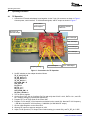
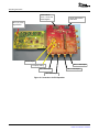
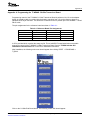
User's Guide
SLWU045 – October 2006
TSW5005 – TI WiMAX 5.6-GHz Transceiver
Contents
1
Introduction ..........................................................................................
2
Release Inventory ..................................................................................
3
System Requirements .............................................................................
4
Operating Procedure ...............................................................................
Appendix A
Programming the TI WiMAX 5.6-GHz Transceiver Board ...........................
1
1
1
2
5
List of Figures
1
2
Connections for TX Operation .................................................................... 2
Connections for RX Operation .................................................................... 4
List of Tables
A-1
1
Reference Board Pin Assignments ............................................................... 5
Introduction
This user’s manual describes the operation of the Texas Instruments TI WiMAX 5.6-GHz Transceiver
Board and Adapter Board. The boards are supplied with a parallel port interface cable and power cable.
Operation of the board requires an external dual-power supply and a personal computer.
2
Release Inventory
The release package contains:
1. TI WiMAX 5.6-GHz Transceiver Board
2. Adapter board
3. Parallel port interface cable
4. Power cable
5. Documentation compact disc (CD)
3
System Requirements
1.
2.
3.
4.
5.
+7.5-V power supply, 1 A
+4.1-V power supply, 1 A
+5-V power supply, 100 mA
Personal computer running Windows™ 98, 2000, or XP
Typical test equipment used for system measurement:
a. Signal generator: Agilent ESG Series (with baseband I/Q modulation option for 802.16x modulated
testing) or equivalent
b. Spectrum analyzer: Agilent PSA Series (with phase noise option) or equivalent
c. Vector signal analyzer: Agilent 89600 Series for 802.16x modulated EVM testing or equivalent
Windows is a trademark of Microsoft Corporation.
LabVIEW is a trademark of National Instruments Corporation.
SLWU045 – October 2006
Submit Documentation Feedback
TSW5005 – TI WiMAX 5.6-GHz Transceiver
1
www.ti.com
Operating Procedure
4
Operating Procedure
4.1
TX Operation
1. Connect the RF board and adapter board together via the 70-pin I/O connector as shown in Figure 1.
Connect power, serial interface, TX I/Q baseband signals, and RF output as shown in Figure 1.
Power Cable to
+7.5-V, +4.1-V, +5-V
Power Supplies
Parallel Port Interface
Cable to PC
RF Out (J 1) to
Spectrum Analyzer
TX Q + Data Input
TX Q - Data Input
TX I + Data Input
TX I - Data Input
I DC Offset Adjust
Q DC Offset Adjust
Frequency Tuning
Figure 1. Connections for TX Operation
2. Set DIP switches on the adapter board as follows:
TX_IF_ALC[1:5] = X
TX_RF_ALC1 = 0
TX_RF_ALC2 = X
TX_RF_ALC3 = 1
RX_GAIN_SW = X
CAL_EN = X
PA_ON = 1
RX_TX_1 = 1
RX_TX_2 = 1
LNA_GAIN_SW = 0
RX_AGC_SLOW = 0
3. Turn on power supplies
4. On the control GUI, click on Configure Par Port and verify that CLOCK = bit 0, DATA = bit 1, and LE =
bit 2. Change settings if required (see Appendix A).
5. Program DUT to ACTIVE mode on the control GUI.
6. Program IF VCO and RF VCO frequencies as desired on the control GUI. Nominal IF VCO frequency
= 398 MHz. Nominal RF VCO frequency = 2998 MHz (for 5600 MHz RF output).
7. Click on Write Registers on the control GUI.
8. Observe RF output on spectrum analyzer or VSA.
9. Adjust TX I/Q input drive, TX Output Power Control setting (on control GUI), and TX_RF_ALC1 DIP
2
TSW5005 – TI WiMAX 5.6-GHz Transceiver
SLWU045 – October 2006
Submit Documentation Feedback
www.ti.com
Operating Procedure
switch (on adapter board) as required for desired TX output power level.
10. Adjust I Offset (R29) and Q Offset (R31) using potentiometers on adapter board to null carrier (for
single tone IQ input) or minimize I/Q offset error (for modulated IQ input).
11. Adjust AFC_ADJ (R34) on adapter board as required to minimize frequency error.
Note:
4.2
For optimum EVM performance, I/Q quadrature of the TX I and TX Q inputs must be
adjusted to minimize quadrature error. I/Q crossover resistors R234, R235, R258, and
R259 can be used to add a fixed quadrature offset to correct for I/Q non-idealities.
Contact TI for further information.
RX Operation
1. Connect the RF board and adapter board together via the 70-pin I/O connector as shown in Figure 2.
Connect power, serial interface, RX I/Q baseband signals, and RF input as shown in Figure 1.
2. Set DIP switches on the adapter board as follows:
TX_IF_ALC[1:5] = X
TX_RF_ALC1 = 0
TX_RF_ALC2 = X
TX_RF_ALC3 = 1
RX_GAIN_SW = X
CAL_EN = 1
PA_ON = 0
RX_TX_1 = 0
RX_TX_2 = 0
LNA_GAIN_SW = 1
RX_AGC_SLOW = 0
3. Verify that RF Signal Source at J1 input is OFF.
4. Turn on power supplies
5. On the control GUI, click on Configure Par Port and verify that CLOCK = Bit 0, DATA = Bit 1, and LE =
Bit 2. Change settings if required (see Appendix A).
6. Program DUT to ACTIVE mode on the control GUI.
7. Program IF VCO and RF VCO frequencies as desired on the control GUI. Nominal IF VCO frequency
= 398 MHz. Nominal RF VCO frequency = 2998 MHz (for 5600 MHz RF output).
8. Click on Write Registers on the control GUI.
9. STATUS light on adapter board should be OFF.
10. Toggle the CAL_EN DIP switch on the adapter board first LOW, then HIGH.
11. STATUS light on adapter board should be ON. Once the STATUS light is ON, the internal DC offset
calibration is active.
12. Set RF Signal Source to desired power level ( < –50 dBm) and frequency, and turn ON.
13. Observe baseband I/Q output either on spectrum analyzer (DC coupled) or VSA.
14. Adjust AGC gain using the RX_AGC potentiometer (R36) on the adapter board for desired baseband
output level. For high level RF input power (–50 dBm to –20 dBm), use the LNA_GAIN_SW and
RX_AGC_SLOW DIP switches to further reduce gain.
15. Adjust AFC_ADJ (R34) on adapter board as required to minimize frequency error.
Note:
For optimum EVM performance, I/Q quadrature of the RF input source must be adjusted
to minimize quadrature error. (No quadrature correction is available in the RX path on the
Transceiver Board).
SLWU045 – October 2006
Submit Documentation Feedback
TSW5005 – TI WiMAX 5.6-GHz Transceiver
3
www.ti.com
Operating Procedure
Power Cable to
+7.5-V, +4.1-V, +5-V
Power Supplies
Parallel Port Interface
Cable to PC
RF In (J1) From
Signal Source
RX AGC Adjust
RX Q + Data Output
Frequency Tuning
RX I - Data Output
RX Q - Data Output
RX I + Data Output
Figure 2. Connections for RX Operation
4
TSW5005 – TI WiMAX 5.6-GHz Transceiver
SLWU045 – October 2006
Submit Documentation Feedback
www.ti.com
Appendix A
Appendix A Programming the TI WiMAX 5.6-GHz Transceiver Board
Programming control of the TI WiMAX 5.6-GHz Transceiver Board is performed via J12 on the adapter
board. An interface cable is provided with the board to transition from J12 on the reference board to a
standard DB-25 style connector. This should be connected to the PC parallel port via a standard 1:1 wired
DB-25 cable.
The pin assignments for the reference board are shown in Table A-1:
Table A-1. Reference Board Pin Assignments
Data Bit
Signal Name
PC DB25 Pin
Ref Board J1 Pin
0
CLK
2
1
1
DATA
3
2
2
LE
4
3
—
GROUND
18
4
A CD is provided which contains the setup.exe file. This a LabVIEW™-based stand-alone executable
program for control of the TI WiMAX 5.6-GHz Transceiver Board. See the TI BWA Labview GUI
Installation Instructions.doc file on the CD for installation instructions.
After installation, the following main menu should appear after clicking START → PROGRAMS →
TI_BWA:
Click on the 5.8 GHz Eval Board button. The following control GUI should appear:
SLWU045 – October 2006
Submit Documentation Feedback
Programming the TI WiMAX 5.6-GHz Transceiver Board
5
www.ti.com
Parallel Port Configuration
All controls needed to program the TI WiMAX 5.6-GHz Transceiver Board are available on the main
screen (identical controls as the TRF2432 chip).See the TRF2432 data sheet (SLWS177) for explanation
of controls. The Actual Output Frequency is shown for convenience only and is the calculated RF
frequency that is generated.
A.1
Parallel Port Configuration
The parallel port address and pin assignments can be modified by clicking on the Configure Par Port
button. The default parallel port address is 378, and the pin assignments must be set to match Table A-1.
To ensure proper operation, ensure that the bit settings are set as follows:
Bit for CLK = 0
Bit for DATA = 1
Bit for LE = 2
A.2
Manual Register Control
Manual bit-by-bit control of all programming registers is available by clicking on the Set Bits Individually
button. The register/bit assignments are in the same order as Table 16 of the data sheet.
After modifying bit settings, press the SEND button next to a register to write the new values to the
TRF2432. Any changes made to the bit settings on this panel are reflected on the main panel when the
manual panel is closed.
CAUTION
Manually modifying bit settings can potentially send invalid control
values. Use at your own risk.
6
Programming the TI WiMAX 5.6-GHz Transceiver Board
SLWU045 – October 2006
Submit Documentation Feedback
www.ti.com
Manual Frequency Control
A.3
Manual Frequency Control
The Manual Freq Control panel allows input of IF/RF register values and any reference frequency. It
calculates the resulting IF VCO and RF VCO frequencies. Pressing the SEND button writes the new
register values to the TRF2432. This panel is intended for use in cases where an external reference
frequency other than 40 MHz or 44 MHz is used.
CAUTION
Manually modifying frequency control registers can potentially send
invalid control values. Use at your own risk.
SLWU045 – October 2006
Submit Documentation Feedback
Programming the TI WiMAX 5.6-GHz Transceiver Board
7
EVALUATION BOARD/KIT IMPORTANT NOTICE
Texas Instruments (TI) provides the enclosed product(s) under the following conditions:
This evaluation board/kit is intended for use for ENGINEERING DEVELOPMENT, DEMONSTRATION, OR EVALUATION
PURPOSES ONLY and is not considered by TI to be a finished end-product fit for general consumer use. Persons handling the
product(s) must have electronics training and observe good engineering practice standards. As such, the goods being provided are
not intended to be complete in terms of required design-, marketing-, and/or manufacturing-related protective considerations,
including product safety and environmental measures typically found in end products that incorporate such semiconductor
components or circuit boards. This evaluation board/kit does not fall within the scope of the European Union directives regarding
electromagnetic compatibility, restricted substances (RoHS), recycling (WEEE), FCC, CE or UL, and therefore may not meet the
technical requirements of these directives or other related directives.
Should this evaluation board/kit not meet the specifications indicated in the User’s Guide, the board/kit may be returned within 30
days from the date of delivery for a full refund. THE FOREGOING WARRANTY IS THE EXCLUSIVE WARRANTY MADE BY
SELLER TO BUYER AND IS IN LIEU OF ALL OTHER WARRANTIES, EXPRESSED, IMPLIED, OR STATUTORY, INCLUDING
ANY WARRANTY OF MERCHANTABILITY OR FITNESS FOR ANY PARTICULAR PURPOSE.
The user assumes all responsibility and liability for proper and safe handling of the goods. Further, the user indemnifies TI from all
claims arising from the handling or use of the goods. Due to the open construction of the product, it is the user’s responsibility to
take any and all appropriate precautions with regard to electrostatic discharge.
EXCEPT TO THE EXTENT OF THE INDEMNITY SET FORTH ABOVE, NEITHER PARTY SHALL BE LIABLE TO THE OTHER
FOR ANY INDIRECT, SPECIAL, INCIDENTAL, OR CONSEQUENTIAL DAMAGES.
TI currently deals with a variety of customers for products, and therefore our arrangement with the user is not exclusive.
TI assumes no liability for applications assistance, customer product design, software performance, or infringement of
patents or services described herein.
Please read the User’s Guide and, specifically, the Warnings and Restrictions notice in the User’s Guide prior to handling the
product. This notice contains important safety information about temperatures and voltages. For additional information on TI’s
environmental and/or safety programs, please contact the TI application engineer or visit www.ti.com/esh.
No license is granted under any patent right or other intellectual property right of TI covering or relating to any machine, process, or
combination in which such TI products or services might be or are used.
FCC Warning
This evaluation board/kit is intended for use for ENGINEERING DEVELOPMENT, DEMONSTRATION, OR EVALUATION
PURPOSES ONLY and is not considered by TI to be a finished end-product fit for general consumer use. It generates, uses, and
can radiate radio frequency energy and has not been tested for compliance with the limits of computing devices pursuant to part 15
of FCC rules, which are designed to provide reasonable protection against radio frequency interference. Operation of this
equipment in other environments may cause interference with radio communications, in which case the user at his own expense
will be required to take whatever measures may be required to correct this interference.
EVM WARNINGS AND RESTRICTIONS
It is important to operate this EVM within the input voltage range of 0 V to 3.3 V and the output voltage range of 0 V to 3.3 V.
Exceeding the specified input range may cause unexpected operation and/or irreversible damage to the EVM. If there are
questions concerning the input range, please contact a TI field representative prior to connecting the input power.
Applying loads outside of the specified output range may result in unintended operation and/or possible permanent damage to the
EVM. Please consult the EVM User's Guide prior to connecting any load to the EVM output. If there is uncertainty as to the load
specification, please contact a TI field representative.
During normal operation, some circuit components may have case temperatures greater than 85°C. The EVM is designed to
operate properly with certain components above 85°C as long as the input and output ranges are maintained. These components
include but are not limited to linear regulators, switching transistors, pass transistors, and current sense resistors. These types of
devices can be identified using the EVM schematic located in the EVM User's Guide. When placing measurement probes near
these devices during operation, please be aware that these devices may be very warm to the touch.
Mailing Address: Texas Instruments, Post Office Box 655303, Dallas, Texas 75265
Copyright © 2006, Texas Instruments Incorporated
IMPORTANT NOTICE
Texas Instruments Incorporated and its subsidiaries (TI) reserve the right to make corrections, modifications, enhancements,
improvements, and other changes to its products and services at any time and to discontinue any product or service without notice.
Customers should obtain the latest relevant information before placing orders and should verify that such information is current and
complete. All products are sold subject to TI’s terms and conditions of sale supplied at the time of order acknowledgment.
TI warrants performance of its hardware products to the specifications applicable at the time of sale in accordance with TI’s
standard warranty. Testing and other quality control techniques are used to the extent TI deems necessary to support this
warranty. Except where mandated by government requirements, testing of all parameters of each product is not necessarily
performed.
TI assumes no liability for applications assistance or customer product design. Customers are responsible for their products and
applications using TI components. To minimize the risks associated with customer products and applications, customers should
provide adequate design and operating safeguards.
TI does not warrant or represent that any license, either express or implied, is granted under any TI patent right, copyright, mask
work right, or other TI intellectual property right relating to any combination, machine, or process in which TI products or services
are used. Information published by TI regarding third-party products or services does not constitute a license from TI to use such
products or services or a warranty or endorsement thereof. Use of such information may require a license from a third party under
the patents or other intellectual property of the third party, or a license from TI under the patents or other intellectual property of TI.
Reproduction of information in TI data books or data sheets is permissible only if reproduction is without alteration and is
accompanied by all associated warranties, conditions, limitations, and notices. Reproduction of this information with alteration is an
unfair and deceptive business practice. TI is not responsible or liable for such altered documentation.
Resale of TI products or services with statements different from or beyond the parameters stated by TI for that product or service
voids all express and any implied warranties for the associated TI product or service and is an unfair and deceptive business
practice. TI is not responsible or liable for any such statements.
TI products are not authorized for use in safety-critical applications (such as life support) where a failure of the TI product would
reasonably be expected to cause severe personal injury or death, unless officers of the parties have executed an agreement
specifically governing such use. Buyers represent that they have all necessary expertise in the safety and regulatory ramifications
of their applications, and acknowledge and agree that they are solely responsible for all legal, regulatory and safety-related
requirements concerning their products and any use of TI products in such safety-critical applications, notwithstanding any
applications-related information or support that may be provided by TI. Further, Buyers must fully indemnify TI and its
representatives against any damages arising out of the use of TI products in such safety-critical applications.
TI products are neither designed nor intended for use in military/aerospace applications or environments unless the TI products are
specifically designated by TI as military-grade or "enhanced plastic." Only products designated by TI as military-grade meet military
specifications. Buyers acknowledge and agree that any such use of TI products which TI has not designated as military-grade is
solely at the Buyer's risk, and that they are solely responsible for compliance with all legal and regulatory requirements in
connection with such use.
TI products are neither designed nor intended for use in automotive applications or environments unless the specific TI products
are designated by TI as compliant with ISO/TS 16949 requirements. Buyers acknowledge and agree that, if they use any
non-designated products in automotive applications, TI will not be responsible for any failure to meet such requirements.
Following are URLs where you can obtain information on other Texas Instruments products and application solutions:
Products
Applications
Amplifiers
amplifier.ti.com
Audio
www.ti.com/audio
Data Converters
dataconverter.ti.com
Automotive
www.ti.com/automotive
DSP
dsp.ti.com
Broadband
www.ti.com/broadband
Interface
interface.ti.com
Digital Control
www.ti.com/digitalcontrol
Logic
logic.ti.com
Military
www.ti.com/military
Power Mgmt
power.ti.com
Optical Networking
www.ti.com/opticalnetwork
Microcontrollers
microcontroller.ti.com
Security
www.ti.com/security
RFID
www.ti-rfid.com
Telephony
www.ti.com/telephony
Low Power
Wireless
www.ti.com/lpw
Video & Imaging
www.ti.com/video
Wireless
www.ti.com/wireless
Mailing Address: Texas Instruments, Post Office Box 655303, Dallas, Texas 75265
Copyright © 2007, Texas Instruments Incorporated