1
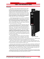
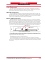
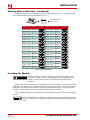
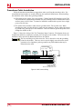
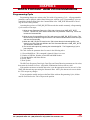
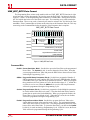
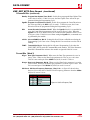
A D V A N C E D
M IC R O C O N T R O L S
7 9 6 1
S S I In t e r f a c e
IN C .
Manual #: 940-59010
M
o d u le
A c c o m p a n y P r o g r a m
o
)
d u
le
U s e r
M
a l
u
a n
G E
- F a n
u c
0
9 0 - 7
I/O
M
GENERAL INFORMATION
Important User Information
The products and application data described in this manual are useful in a wide variety of different applications. Therefore, the user and others responsible for applying these products described
herein are responsible for determining the acceptability for each application. While efforts have
been made to provide accurate information within this manual, AMCI assumes no responsibility
for the application or the completeness of the information contained herein.
UNDER NO CIRCUMSTANCES WILL ADVANCED MICRO CONTROLS, INC. BE
RESPONSIBLE OR LIABLE FOR ANY DAMAGES OR LOSSES, INCLUDING INDIRECT
OR CONSEQUENTIAL DAMAGES OR LOSSES, ARISING FROM THE USE OF ANY
INFORMATION CONTAINED WITHIN THIS MANUAL, OR THE USE OF ANY PRODUCTS
OR SERVICES REFERENCED HEREIN.
Throughout this manual the following two notices are used to highlight important points.
WARNINGS tell you when people may be hurt or equipment may be dam-
aged if the procedure is not followed properly.
CAUTIONS tell you when equipment may be damaged if the procedure is
not followed properly.
No patent liability is assumed by AMCI, with respect to use of information, circuits, equipment,
or software described in this manual.
The information contained within this manual is subject to change without notice.
Standard Warranty
ADVANCED MICRO CONTROLS, INC. warrants that all equipment manufactured by it will
be free from defects, under normal use, in materials and workmanship for a period of [1] year.
Within this warranty period, AMCI shall, at its option, repair or replace, free of charge, any equipment covered by this warranty which is returned, shipping charges prepaid, within one year from
date of invoice, and which upon examination proves to be defective in material or workmanship
and not caused by accident, misuse, neglect, alteration, improper installation or improper testing.
The provisions of the "STANDARD WARRANTY" are the sole obligations of AMCI and
excludes all other warranties expressed or implied. In no event shall AMCI be liable for incidental
or consequential damages or for delay in performance of this warranty.
Returns Policy
All equipment being returned to AMCI for repair or replacement, regardless of warranty status,
must have a Return Merchandise Authorization number issued by AMCI. Call (860) 585-1254
with the model number and serial number (if applicable) along with a description of the problem.
A "RMA" number will be issued. Equipment must be shipped to AMCI with transportation
charges prepaid. Title and risk of loss or damage remains with the customer until shipment is
received by AMCI.
24 Hour Technical Support Number
24 Hour technical support is available on this product. For technical support, call (860) 5837271. Your call will be answered by the factory during regular business hours, Monday through
Friday, 8AM - 5PM EST. During non-business hours an automated system will ask you to enter
the telephone number you can be reached at. Please remember to include your area code. The system will page one of two engineers on call. Please have your product model number and a description of the problem ready before you call.
ADVANCED MICRO CONTROLS INC.
ABOUT THIS MANUAL
Introduction
This manual explains the operation, installation, and programming of the 7961 SSI Interface
Module for the GE Fanuc Series 90™-70 programmable controller systems. Designed specifically
for transducers that use the SSI protocol, the programmable features of the 7961 make it an efficient interface between any SSI transducer and the 90-70 processors.
It is strongly recommended that you read the following instructions. If there are any unanswered questions after reading this manual, call the factory. An applications engineer will be
available to assist you.
“AMCI” is a registered trademark of Advanced Micro Controls Inc.
The AMCI logo is a trademark of Advanced Micro Controls Inc.
“Series 90” is a trademark of GE Fanuc Automation North America
“Temposonics” is a registered trademark of MTS Systems Corporation
Manuals at AMCI are constantly evolving entities. Your questions and comments on this manual and the information it contains are both welcomed and necessary if this manual is to be
improved. Please direct all comments to: Technical Documentation, AMCI, 20 Gear Drive, Plymouth Industrial Park, Terryville CT 06786, or fax us at (860) 584-1973.
Revision Record
The following is the revision history for this manual. In addition to the information listed here,
revisions will fix any known typographical errors and clarification notes may be added.
This manual, 940-09010, is the initial release of the manual. It corresponds to hardware revision B, and software revision 0, checksum CC02.
20 Gear Drive, Plymouth Ind. Park, Terryville, CT 06786
Tel: (860) 585-1254 Fax: (860) 584-1973 http:\\www.amcicontrols.com
3
7961 SPECIFICATIONS
Module Interface
Third party VME module. Fully compatible
with GE Fanuc’s Industrialized VMEbus
(VME-I).
Compatible Transducers
Any transducer that outputs data in single
word SSI format. Number of bits transferred is programmable from 1 to 32.
Multi-word transfers are not supported.
Transducer Input Isolation
Optically Isolated (1500 Vac)
Programmable Parameters
SSI Setup Parameters –
SSI Clock Frequency
Number of SSI Bits
Number of Data Bits
MSB Number
Data Type
Data Logic
Data Setup Parameters –
Scalar Multiplier
Scalar Divisor
Preset Value
Count Direction
Rate Update Time
Data Value (position) Range
±268,435,455 counts max.
Data Value (position) Preset
Data Value can be preset to any value within
the range of ±268,435,455.
Rate of Change (velocity) Range
±268,435,455 counts per second max.
4
Rate of Change (velocity) Resolution
Determined by, and identical to, the Data
Value resolution.
Rate of Change (velocity) Update Time
Programmable from 1 millisecond to 1,000
milliseconds with 1 millisecond resolution.
Data Transfer
Programmed with a sixteen byte VME WRT
BYTE instruction.
Data available with a sixteen byte VME RD
BYTE instruction.
Data Available to Processor
Data Value, Rate of Change, status bits, and
raw SSI data.
Program Storage
Non-volatile RAM. Integrated lithium battery is rated for ten years.
Backplane Power Requirements
+5 Vdc @ 0.550A (2.75 Watts)
Transducer Power Supply
External +24 Vdc supply needed for transducer operation.
Modules +5 Vdc Supply Fuse
3.5A Fast Blow (Littelfuse 22503.5)
Environmental Conditions
Operating Temperature: 0 to 60° C
Relative Humidity:
5 to 95%
(non-condensing)
Storage Temperature: -40 to 85° C
ADVANCED MICRO CONTROLS INC.
CHAPTER 1
7961 INTRODUCTION
Overview
The single slot 7961 SSI Interface Module accepts a single
transducer input and plugs directly into the GE Fanuc 90-70
rack. The 7961 module reads and scales the data from any SSI
transducer and also calculates the data’s rate of change. The
meaning of the Data Value and Rate Of Change information
depends on the type of transducer attached to the 7961. A SSI
pressure sensor reports a pressure value and the 7961 calculates
the pressure change per second. A SSI position sensor reports a
position value and the 7961 calculates the position change per
second, which is the velocity, of the moving part.
Communicating with eight word, (sixteen byte) VME READ
BYTE and VME WRITE BYTE instructions, the 7961 reports
the Data Value, Rate Of Change, and actual SSI data to the 90-70
CPU. The Data Value has a range of ±268,435,455 counts,
which is twenty-eight bits plus sign. The Rate of Change has a
range of ±268,435,455 counts per second, with the value negative when the Data Value is decreasing.
One type of SSI transducer the 7961 can interface with is the
linear displacement transducer (LDT). LDTs are non-contact,
absolute linear measurement devices that offer high resolution
and accuracy. The transducer tracks the absolute position of a
magnet along its waveguide. LDTs can be manufactured with a
waveguide length from 2 to 300 inches. There are two major
manufacturers of SSI linear displacement transducers, Balluff
and MTS. Presently, Balluff BTL-5 transducers offer a resolution
and repeatability of up to 5 µm (0.0002") and an accuracy of up
to ±30 µm (±0.0012"). MTS Temposonics III transducers offer a
resolution and repeatability of up to 5 µm (0.0002") and an accuracy of up to 50 µm (0.002").
The formal SSI protocol defines a twenty-five bit serial data
Figure 1.1 7961 Module
stream from the transducer that is synchronized to clock pulses
generated by the controller. However, AMCI is aware of some
transducers that do not transmit twenty-five bits. To accommodate these devices, AMCI has made
the number of bits that the module accepts programmable from one to thirty-two.
Physically, the 7961 module is a single slot module that accepts a single SSI transducer, and
requires an external 24 Vdc power supply. In addition to the eight pin Transducer Input Connector,
the front panel has two LED’s that show the modules’ status.
The 7961’s Programmable Parameters are used to define where the SSI data is embedded in the
bit stream and gives you the ability to scale this data. For example, assume that you are using a
Balluff LDT that gives you one count per 20 µm. You can use the 7961 to scale this value to one
count per 0.001 inch. The calculated Rate of Change is scaled to the same units as the Data Value.
To continue the example, the Rate of Change (velocity) is scaled thousandths of an inch per second. All parameter values are stored in non-volatile nvRAM memory.
Along with the scaled Data Value and Rate of Change information, the 7961 reports the actual
SSI data to the 90-70 processor. This gives you the ability to use ladder logic to check the SSI data
for any additional information that it may contain, such as error bits.
20 Gear Drive, Plymouth Ind. Park, Terryville, CT 06786
Tel: (860) 585-1254 Fax: (860) 584-1973 http:\\www.amcicontrols.com
5
1
INTRODUCTION
SSI Protocol
Figure 1.2 shows how a 7961 module reads data from a SSI transducer. Note that the formal
SSI definition allows for twenty-four bits of data and a twenty-fifth stop bit. However, AMCI is
aware of some transducers that transmit more or less than twenty-five bits. To accommodate these
transducers, the 7961 can be programmed to accept up to thirty-two bits in the SSI bit stream.
TINT
➀
➂
➁
1
2
3
n-1
n
TIDL
TM
1
2
3
CLOCK
DATA
Bit 1
Bit 2
Bit 3
Bit n-1
Bit n
Stop
Bit 1
Bit 2
Bit 3
“n” = Number of bits in SSI data. Range of 1 to 32. Default of 24.
➀ The first falling edge of the clock signal latches the SSI data. Note: Some transducers
latch the data at the end of the previous interrogation.
➁ The next “n” rising edges of the clock shift out the “n” data bits.
➂ TINT is the time between interrogations and is fixed by the module at 500µS. TM is the
time that the Stop bit is valid, which is typically 12 to 20 µS. TIDL is the time between
the end of the last interrogation and the start of the next. The transducer must have
new data available within the TIDL Time period if the system is to work properly. The
table below gives the values of TIDL for twenty-four and thirty-two bit SSI data transfers at the four different clock frequencies available with the module.
ClockFRQ TIDL @ 24 bits TIDL @ 32 bits
125 KHz
250 KHz
500 KHz
1.00 MHz
308µS
404µS
452µS
476µS
244µS
372µS
436µS
468µS
Figure 1.2 SSI Data Stream Format
The formal SSI protocol definition includes a multi-word transfer capability.
This is accomplished by holding the clock signal low for the TM time period and
restarting the clock. This signals the transducer to transfer additional bits of data
instead of restarting at bit 1. The 7961 does not support multi-word transfers.
Programmable Parameters
The 7961 module is setup by programming its Programmable Parameters. These parameters are
broken down into two groups.
h SSI Setup Parameters – Six parameters that are used to extract the SSI data from the
twenty-five bit stream. These parameters define the clock speed of the data transfer, the
position and length of the SSI data within the bit stream, and the format of the data.
h Data Setup Parameters – Five parameters that affect the Data Value and Rate of Change
information. These parameters allow you to scale the Data Value, preset it to a programmable count, and set the update time of the Rate of Change information.
6
ADVANCED MICRO CONTROLS INC.
1
INTRODUCTION
SSI Setup Parameters
SSI Clock Frequency
This parameter allows you to set the SSI clock frequency to one of four values: 125 KHz, 250
KHz, 500 KHz, or 1.000 MHz.
The default value of 125 KHz will work in all applications. Setting the clock frequency to 1 MHz yields the longest idle times between interrogations. However,
your transducer may not be able to operate at 1 MHz. Consult your transducer
documentation to determine its maximum operating frequency. Remember that
the maximum SSI clock frequency is also dependent on the length of the transducer cable.
Number of SSI Bits
This value sets the number of bits that the 7961 will read from the SSI transducer per interogation. The parameters default value of twenty-four will work in most cases. You can set this parameter to any value between 1 and 32.
Number of Data Bits &
MSB Number Parameters
As the examples show in figure 1.3, these two parameters tell the 7961 where the SSI data is
embedded in the SSI data stream. The Number of Data Bits parameter specifies the length of the
data and the MSB Number parameter specifies the bit that starts the SSI data. The default value
for the Number of Data Bits parameter is twenty-four. The default value of the MSB Number
parameter is one.
SSI DATA BITS
1 2 3 4 5 6 7 8 9 10 11 12 13 14 15 16 17 18 19 20 21 22 23 24
16 Bit Data Value
20 Bit Data Value
n-1 n
Number of Data Bits = 16
MSB Number = 9
Number of Data Bits = 20
MSB Number = 1
Maximum Value of “n” is 32
Figure 1.3 Embedded Data Value
Refer to the documentation that came with your transducer to determine where the SSI data is
located in the SSI data stream. If you are using a Balluff LDT, the default values should work correctly. If you are using a MTS LDT, Set the Number of Data Bits equal to the LDT’s number of
bits and the MSB Number to one.
Data Type
This parameter tells the 7961 to interpret the SSI data as a binary number or a gray code number. The default value is Binary.
Data Logic
This parameter is included to handle situations where the SSI data is reported with negative
logic. If this parameter is set, the 7961 will assume the SSI data is reported with negative logic and
will invert the data bits before performing any scaling. The default value is positive logic. When
this parameter is left at its default value, the 7961 will use the SSI data as it is from the transducer.
20 Gear Drive, Plymouth Ind. Park, Terryville, CT 06786
Tel: (860) 585-1254 Fax: (860) 584-1973 http:\\www.amcicontrols.com
7
1
INTRODUCTION
Data Setup Parameters
Once the 7961 has extracted the SSI data from the SSI data stream, it uses the Data Setup
Parameters to convert the raw SSI data into the Data Value reported to the processor. The formula
for determining the Data Value is:
Data Value = SSI Data * (MUL / DIV) + LO
where: MUL = Scalar Multiplier
DIV = Scalar Divisor
LO = Linear Offset. The Linear Offset is an internal parameter that normally
equals zero. The Linear Offset is changed when you preset the Data Value.
Scalar Multiplier &
Scalar Divisor
These two parameters are use to scale the SSI data. Both parameters have a default value of one
and can range in value from 1 to 32,767. The Scalar Multiplier must be less than or equal to the
Scalar Divisor. In other words, the ratio of Multiplier to Divisor cannot be greater than one.
Linear displacement transducers from Balluff and MTS have resolutions measured in µm/count.
The 7961 can easily convert to a more familiar inch measurement system. The figure below shows
the Multiplier and Divisor values needed to convert from various metric resolutions to inch resolutions. For example, to convert data from a LDT with 5µm/count resolution to 0.0005"/count resolution, use a Multiplier of 50 and a Divisor of 127.
LDT Resolution
Desired Resolution
0.0002" 0.0005"
125
50
5 µm
127
127
100
10 µm
127
20 µm
40 µm
0.001"
25
127
50
127
100
127
0.002"
25
254
25
127
50
127
100
127
0.005"
5
127
10
127
20
127
40
127
= Desired resolution
exceeds resolution
of LDT.
Figure 1.4 Scalar Values for Linear Measurement Conversion
Preset Value
The Preset Value parameter gives you the ability to offset the Data Value. When you preset the
Data Value, the 7961 calculates an internal parameter called the Linear Offset. The Linear Offset
is the value needed to make the Data Value equal to the Preset Value. The default Preset Value is
zero. Its range is ±268,435,455.
1) Programming this parameter does not change the Data Value. There is a
separate command for presetting the Data Value to the Preset Value.
2) The 7961 will issue a Preset Error message if you attempt to program a
Preset Value that is outside its range of ±268,435,455.
3) Presetting the Data Value generates a linear offset. If you are using a
rotary encoder and wish to preset the position, contact AMCI for assistance
in developing the ladder logic needed to offset the Data Value in the PLC.
8
ADVANCED MICRO CONTROLS INC.
INTRODUCTION
1
Data Setup Parameters (continued)
Count Direction
This parameter is useful if your Data Value represents a linear position. It gives you the ability
to reverse the direction of motion needed to increase the position count. For simplicity’s sake, the
two values for this parameter are called Positive Direction and Negative Direction. When this
parameter is set to its default of Positive, the Data Value is not changed. When this parameter is set
to Negative, the Data Value is changed to: (2n - (Data Value)), where ‘n’ is the programmed value
of the Number of Data Bits parameter.
If your Data Value represents a rotary position, you can change the count direction with this
parameter only if the number of counts in your Data Value is a power of two. If it is not, you can
easily reverse the count direction with ladder logic.
1) Subtract the Data Value from the number of encoder counts and store it in a temporary
register.
2) If the Data Value equals zero, then move zero into your temporary register.
Rate Update Time
The Rate Update time sets the amount of time between Rate of Change information updates to
the processor. Its range of values is 1 to 1,000 mS, with a default of 100 mS. Decrease the time
between updates for fast response to changes in this value. Increase the time between updates for
better averaging of this value.
20 Gear Drive, Plymouth Ind. Park, Terryville, CT 06786
Tel: (860) 585-1254 Fax: (860) 584-1973 http:\\www.amcicontrols.com
9
1
INTRODUCTION
Notes
10
ADVANCED MICRO CONTROLS INC.
CHAPTER 2
INSTALLATION
Power Requirements
The 7961 draws its power from the I/O rack +5Vdc supply. The maximum current draw is
0.550 amps. Therefore, the maximum power draw is 2.75 watts. Add this to the power requirements of all the other modules in the chassis when sizing the power supply.
AM Code Configuration
Every 7961 is factory configured to respond to the address modifier (AM) code of 29h. This
AM code stands for Short (16 bit address) Non-Privileged VME access and is the default used by
GE-Fanuc Series 90-70 systems. For GE-Fanuc installations, you need only set the slot number
(address range) with DIP switches located on the back of the module.
Memory Address Allocation
The DIP switch block on the back of the module, (see figure 2.1), sets the memory addresses
that the 7961 responds to. GE Fanuc assigns default memory locations for each slot in an I/O rack
that should be used in most applications. However, GE Fanuc has also set aside a User Defined
Memory Area from address 5000h to FFFFh in each rack. This memory area can be used by the
7961 if another module in the rack is using the memory addresses that are normally assigned to the
7961’s slot. All 7961 module ship from the factory configured for use in slot 2 of the I/O rack.
3.5 Amp Fuse
DIP Switches
1 2 3 4 5
Figure 2.1 DIP Switch and Fuse Location
The five DIP switches correspond to address lines A15 through A11 on the backplane. If you
are configuring the module to respond to the default memory locations, the DIP switches also represent the slot number of the module in binary.
The starting memory location of the 7961 in binary is:
XXXX X000 0000 0000b, where: XXXX X are the values specified by the DIP switches.
Table 2.1 on the following page gives the DIP switch setting for all of the memory locations that
the 7961 can be configured for. The GE Fanuc slot numbers associated with the memory locations
are also listed.
20 Gear Drive, Plymouth Ind. Park, Terryville, CT 06786
Tel: (860) 585-1254 Fax: (860) 584-1973 http:\\www.amcicontrols.com
11
2
INSTALLATION
Memory Address Allocation (continued)
Setting the switch lever towards the PC board sets the address bit to a “0”. Setting the switch
lever toward the metal case sets the address bit to a “1”.
1 2 3 4 5
Memory Locations GE Slot #
DIP Switch
Slot 5 Default Address
2800h - 2FFFh
Memory Locations GE Slot #
0000h - 07FFh
None
8000h - 87FFh
User Def.
0800h - 0FFFh
None
8800h - 8FFFh
User Def.
1000h - 17FFh
2
9000h - 97FFh
Used Def.
1800h - 1FFFh
3
9800h - 9FFFh
User Def.
2000h - 27FFh
4
A000h - A7FFh
User Def.
2800h - 2FFFh
5
A800h - AFFFh
User Def.
3000h - 37FFh
6
B000h - B7FFh
User Def.
3800h - 3FFFh
7
B800h - BFFFh
User Def.
4000h - 47FFh
8
C000h - C7FFh
User Def.
4800h - 4FFFh
9
C800h - CFFFh
User Def.
5000h - 57FFh
User Def.
D000h - D7FFh
User Def.
5800h - 5FFFh
User Def.
D800h - DFFFh
User Def.
6000h - 67FFh
User Def.
E000h - E7FFh
User Def.
6800h - 6FFFh
User Def.
E800h - EFFFh
User Def.
7000h - 77FFh
User Def.
F000h - F7FFh
User Def.
7800h - 7FFFh
User Def.
F800h - FFFFh
User Def.
DIP Switch
Table 2.1 DIP Switch Settings
Installing the Module
Remove system power before removing or installing any module in an
I/O chassis. Failure to observe this warning may result in damage to the
module’s circuitry and/or undesired operation with possible injury to
personnel.
After selecting the proper addresses with the DIP switches, the module is ready to be installed
in the I/O rack. Insert the P.C. board into the card guides and gently seat the P1 connector into the
backplane. Seating the connector does not require a great amount of force. Applying to much
pressure on a mis-aligned connector may damage the module or backplane.
After seating the module in the backplane, secure the module to the rack with the two mounting
screws.
The two mounting screws that secure the module are also the grounding points for
the 7961. These two screws must be tightly screwed into the rack for proper operation.
12
ADVANCED MICRO CONTROLS INC.
2
INSTALLATION
Front Panel Description
The front panel of the 7961 has the eight pin Transducer Input Connector and the two status
LED’s. The mate to the Transducer Input Connector is a Phoenix Contact MSTB2.5/8-ST-5.08,
AMCI part number MS-8, which is included with the module.
Status LED’s
The green and red LED’s show the modules’ operating status.
h RUN - This green LED is on when the module is operational.
h FAULT - This red LED is on if the module fails its initialization routines. If this occurs,
remove the transducer connector and cycle power to the module. If the fault remains, check
the VME READ BYTE data to see if there is a nvRAM error. If there is, clear the error with
a VME WRITE BYTE instruction. If the error remains, the module needs to be repaired.
See the inside front cover for information on contacting AMCI.
The 7961 considers all of the SSI bits as potential data. Therefore, the 7961 cannot determine if there is a transducer error. If your SSI transducer has error bits
embedded in the SSI data, your ladder logic should check these bits. They are
available in the raw SSI data the 7961 transmits to the processor. If the transducer is not attached to the 7961, the SSI data will be all 1’s. If you know that
your SSI data can never be all 1’s, use this as a check to see if the transducer is
attached and working.
Compatible Transducers
The 7961 module is compatible with any transducer that outputs serial data using the SSI protocol. The 7961 has been tested with Balluff BTL-3 and MTS Temposonics III linear displacement
transducers, Stegmann optical encoders, and SICK optical distance sensors. Note that the 7961
does not support multi-word SSI transfers. Even though the SSI definition includes the multi-word
transfer, it is rarely used in actual applications.
Transducer Mounting
Follow the mounting instruction you received with your SSI compatible transducer.
Transducer Power Supply
An external, isolated +24 Vdc supply is needed to power the SSI interface. The supply outputs
must be isolate from chassis ground to eliminate the potential of ground loops. The 7961 draws a
maximum of 0.030 amps to power its opto-couplers. Add this to the current requirements of the
transducer when sizing the +24 Vdc supply.
20 Gear Drive, Plymouth Ind. Park, Terryville, CT 06786
Tel: (860) 585-1254 Fax: (860) 584-1973 http:\\www.amcicontrols.com
13
2
INSTALLATION
Transducer Cable Installation
Follow the transducer manufacturers suggestions when specifying the transducer cable. Preassembled and tested cables are usually offered by the transducer manufacturer. When installing
the transducer cable, follow these general guidelines.
h SSI signals are low voltage, low power signals. Cabling from the SSI transducer to the 7961
can be installed in conduit along with other low power cabling such as communication cables
and low power ac/dc I/O lines. It cannot be installed in conduit with ac power lines or high
power ac/dc I/O lines.
h The shields of the transducer cable must be grounded at the 7961 module only! When
installing the cable, treat the shield as a signal carrying conductor. Do not connect the shield
to ground at any junction box or the transducer. This will eliminate ground loops that could
damage the module or PLC.
Figure 2.2 shows the wiring of the 7961 Transducer Input Connector. The diagram shows pin
assignments and how to connect the external +24 Vdc supply to the module. The color codes for
transducer cables specified by Balluff and MTS are also shown.
The two mounting screws that secure the 7961 to the rack are also the grounding
points for the module. These two screws must be tightly screwed into the rack to
guarantees a low impedance path to ground for any EMI radiation that may be
induced into the cable.
Power Supply
Vdc COM +24Vdc
MTS
TEMPOSONICS
III
BALLUFF
BTL-5
BROWN
WHITE
BLUE
SHIELDS
YELLOW
GREEN
GRAY
PINK
BROWN
BLUE
WHITE
SHIELDS
YELLOW
PINK
GREEN
GRAY
Chassis
GND
+24 Vdc
SUPPLY COM
SHIELDS
+ CLK
– CLK
– DATA
+ DATA
1
2
3
4
5
6
7
8
Module Connector
AMCI Part #: MS-8
Phoenix #: MSTB2.5/8-ST-5.08
Figure 2.2 7961 Connector Wiring
14
ADVANCED MICRO CONTROLS INC.
CHAPTER 3
VME READ/WRITE FUNCTIONS
You will use the VME READ BYTE and VME WRITE BYTE functions to communicate
with the 7961. Acknowledging that you may not be familiar with the VME_RD_BYTE
and VME_WRT_BYTE functions, this chapter introduces both of them. This chapter
also contains information on transfer lengths and addressing specific to the 7961 so you
will need to look over this chapter even if you are familiar with the two instructions.
VME READ BYTE Function
The VME READ BYTE (VME_RD_BYTE) function is used to read the Data Value, Rate of
Change, and raw SSI data from the 7961 to the 90-70 processor. Figure 3.1 is an example of a
VME_RD_BYTE function. The highlighted sections contain information that you must supply
when entering the function.
%I00001
%Q00001
VME_RD_
BYTE
CONST
0029
(
)
AM
LEN
00016
CONST
00003800
ADR
Q
%R00001
Figure 3.1 GE-Fanuc VME_RD_BYTE Function
There are two VME READ functions, one for transferring bytes of data and one for
transferring words. The VME_RD_WORD function will not work with the 7961.
You must use the VME_RD_BYTE function.
Parts of the VME_RD_BYTE Function
Contact Input (%I00001)
Any type of contact can be used to enable the VME_RD function. In this example, the 7961 is
read by the CPU whenever contact %I00001 is a logic “1” and the rung is scanned. You can omit
the contact if you plan to read the 7961 every scan.
Coil Output (%Q00001)
The coil output becomes true when the VME_RD function completes successfully. Any type of
coil can be used. In this example, coil %Q00001 becomes true when the transfer is complete.
You should use a coil output with the VME_RD function. This will allow you to test the coil at
a later point in the scan to be sure that the transfer has completed successfully and the data is valid.
AM (Address Modifier) Code
All 7961’s are factory configured to respond to AM Code 29h. This corresponds to the Standard Short Non-Privileged VME access (16 bit address). The actual AM Code programmed into
the VME_RD function depends on the rack that the module resides in. Table 3.1 on the following
page lists the AM Codes for the different racks. Note that the module remains configured for the
AM Code 29h. The GE Fanuc Expansion Module that controls the expansion rack converts the
AM Code to 29h before it accesses the modules in its rack.
20 Gear Drive, Plymouth Ind. Park, Terryville, CT 06786
Tel: (860) 585-1254 Fax: (860) 584-1973 http:\\www.amcicontrols.com
15
3
VME READ/WRITE
Parts of the VME_RD_BYTE Function (continued)
AM (Address Modifier) Code (continued)
Rack
VME_RD
7961
Number
AM Code AM Code
0
29h
29h
1
1Eh
29h
2
1Dh
29h
3
1Ch
29h
4
1Bh
29h
5
1Ah
29h
6
19h
29h
7
18h
29h
AM Code 1Fh is reserved
Table 3.1 Address Modifier (AM) Codes
Length Parameter
The Length parameter tells the CPU how many bytes to transfer from the module that the
VME_RD targets. For the 7961, this parameter must always be set to sixteen.
Memory Address
This parameter is the starting memory address of the module. For the 7961 this parameter must
be set to the address specified by the DIP switches on the back of the module. See Memory
Address Allocation, starting on page 11 for information on setting the DIP Switches. Table 3.2
below lists the starting address of the 7961 if you use GE Fanuc’s default memory locations for the
slot. Refer to Table 2.1, DIP Switch Settings on page 12 for the possible starting addresses of the
module if you use the User Defined memory addresses available in the rack.
Starting
Starting
Slot
Address
Address
PS
None
5
2800h
1
None
6
3000h
2
1000h
7
3800h
3
1800h
8
4000h
4
2000h
9
4800h
User Defined: See Table 2.1, page 12
Slot
Table 3.2 VME_RD_BYTE Memory Address Allocations
Q: (Transfer Destination Address)
“Q” specifies the first location in the CPU user reference into which data read from the 7961 is
to be stored. In this example, the 7961 data will be stored starting at the first Register Memory
address. Note that eight Register Memory words, (1 through 8 in this example), will be used
because the transfer is sixteen bytes long.
16
ADVANCED MICRO CONTROLS INC.
3
VME READ/WRITE
VME WRITE BYTE Function
The VME WRITE BYTE (VME_WRT_BYTE) function is used to write programming data
from the 90-70 processor to the 7961. Figure 3.2 shows an example of the VME_WRT_BYTE
function. The highlighted sections contain information that you must supply when entering the
function.
%I00001
VME_WRT
_BYTE
%R00030
%Q00001
(
)
IN
LEN
00016
CONST
0029
CONST
00003800
AM
ADR
Figure 3.2 GE Fanuc’s VME_WRT_BYTE Function
There are two VME WRITE functions, one for transferring bytes of data and one
for transferring words. The VME_WRT_WORD function will not work with the
7961. You must use the VME_WRT_BYTE function.
You will use two VME_WRT_BYTE functions to write programming data to the
7961. The first writes fourteen bytes of Parameter Data and the second writes two
bytes of Command Bits. The Parameter Data must be written to the 7961 first.
Parts of the VME_WRT_BYTE Function
Contact Input (%I00002)
Any type of contact can be used to enable the VME_WRT_BYTE function. In this example, the
programming data is sent to the 7961 whenever contact %I0002 is a logic one while the rung is
scanned.
Coil Output (%Q00002)
The coil output becomes true when the VME-WRT_BYTE completes successfully. Any type of
coil can be used.
You should use a coil output with any VME_WRT function. This will allow you to
test the coil at a later point in the scan to see if the function completed successfully.
Input Registers (%R00031)
The starting address of the registers that contain the data to be sent to the module. In the case of
the 7961, this will be programming data to configure the module. If you are transferring a single
word, a constant can be entered instead of a register address.
20 Gear Drive, Plymouth Ind. Park, Terryville, CT 06786
Tel: (860) 585-1254 Fax: (860) 584-1973 http:\\www.amcicontrols.com
17
3
VME READ/WRITE
Parts of the VME_WRT_BYTE Function (continued)
AM (Address Modifier) Code
All 7961’s are factory configured to respond to AM Code 29h. This corresponds to the Standard Short Non-Privileged VME access (16 bit address). The actual AM Code programmed into
the VME_WRT function depends on the rack that the module resides in. Table 3.3 on the following page lists the AM Codes for the different racks. Note that the module remains configured for
the AM Code 29h. The GE Fanuc Expansion Module that controls the expansion rack converts the
AM Code to 29h before it accesses the modules in its rack.
Rack
VME_RD
7961
Number
AM Code AM Code
0
29h
29h
1
1Eh
29h
2
1Dh
29h
3
1Ch
29h
4
1Bh
29h
5
1Ah
29h
6
19h
29h
7
18h
29h
AM Code 1Fh is reserved
Table 3.3 Address Modifier (AM) Codes
Length Parameter
The Length parameter tells the CPU how many bytes to transfer to the module that is targeted by
the VME_WRT. For the 7961, this parameter will either be fourteen or two, depending on the data
that you are sending to the module.
Memory Address
The starting address for the programming data is 80h above the address that the 7961 is configured for. The two bytes of Command Bits start at this address. The fourteen bytes of Parameter
Data starts at 82h above the configured address. Table below gives the starting addresses for the
Parameter Data and Command Bits if you configure the module to use the default addresses
assigned to the slot. If you use a 2K region of the User Defined Memory Addresses, refer to table
2.1 on page 12 for a listing of the available base addresses.
Slot
2
3
4
5
6
7
8
9
User Defined
Parameter Data
1082h
1882h
2082h
2882h
3082h
3882h
4082h
4882h
Base Address+82h
Command Bits
1080h
1880h
2080h
2880h
3080h
3880h
4080h
4880h
Base Address+80h
Table 3.4 VME_WRT_BYTE Memory Address Allocations
18
ADVANCED MICRO CONTROLS INC.
CHAPTER 4
DATA FORMAT AND PROGRAMMING
Programming Cycle
Programming changes are written to the 7961 with a Programming Cycle. All programmable
parameters can be changed, and the Data Value preset, with one cycle. Programming Cycles are
controlled with the Transmit Bit in the Command Bits of the VME_WRT data and the Acknowledge Bit in the VME_RD data.
Assuming that you have a VME_RD_BYTE that reads the module constantly, a Programming
Cycle consists of four steps.
1) Write the new Parameter Data to the 7961 with a fourteen byte VME_WRT_BYTE
function. This block of seven words contains the new parameter values only. It does not
include the Command Bits.
2) Write the new Command Bits to the 7961 with a two byte VME_RD_BYTE function This
two word block contains the flags that tell the 7961 what Parameter Data it should act upon
and sets the Transmit Bit.
3) When the VME_RD_BYTE data from the 7961 shows that the Acknowledge Bit is set,
check for any errors and write 0000h to the 7961 Command Bits with a VME_WRT_BYTE.
This resets the Transmit Bit
4) The module will respond by resetting the Acknowledge Bit. The Programming Cycle is
now complete.
The 7961 checks the parameter data for errors in the following order:
1)
2)
3)
4)
5)
Clear nvRAM Error. This command is ignored if there is no error
Number of SSI Bits, Number of Data Bits and MSB Number
Scalar Multiplier and Scalar Divisor
Preset Value
Rate Update
The SSI Clock Frequency, Data Logic, Data Type and Count Direction parameters are bit values
that cannot be checked for errors. All possible combinations for these bits are valid.
If the module encounters an invalid data value, it sets the appropriate error bit in word 1 of the
VME_RD data and stops processing the Parameter Data. All of your data must be correct before
the 7961 accepts any changes.
If you program the module and preset the Data Value with one Programming Cycle, all data
must be correct before the 7961 will preset the position.
20 Gear Drive, Plymouth Ind. Park, Terryville, CT 06786
Tel: (860) 585-1254 Fax: (860) 584-1973 http:\\www.amcicontrols.com
19
4
DATA FORMAT
VME_WRT_BYTE Data Format
The Programming Data, written to the module with two VME_WRT_BYTE functions is eight
words long and is used to program the 7961 and/or preset the Data Value. Its format is shown in
figure 4.1. Word 1 of the Programming Data contains the Command Bits. Setting these bits tells
the 7961 which data in the rest of the block to act upon. The remaining seven words contain the
Parameter Data. These seven words, (fourteen bytes) must be written to the 7961 before the Command Bits. If the Command Bits are written at the same time as the Parameter Data, the 7961 may
start acting on the Command Bits before the transfer of the Parameter data is complete.
VME_WRT_BYTE Data Format
SSISet
PrstDV
PrstVal
Scalars
RateUp
DIR
0 0 0 0 0 0 0
PgmDir
nvRClr
SSI
Word 3 Clock
MSB Number
(1 to 32)
DType
Number of SSI Bits (1 to 32)
Word 2
DLogic
Word 1
TRMT
16 15 14 13 12 11 10 09 08 07 06 05 04 03 02 01
0
Num. of Data Bits
(1 to 28)
Word 4
Scalar Multiplier (1 to 32,767)
Word 5
Scalar Divisor (1 to 32,767)
Word 6
Word 7
Preset Value
Signed Double Precision Format
(±268,435,455)
Word 8
Rate Update Time in mS (1 to 1,000)
Figure 4.1 VME_WRT Data Format
Command Bits
PrstDV: Preset Data Value: Bit 01. Set this bit to preset the Data Value to the programmed
Preset Value. The PrstVal bit (04), is used to change the Preset Value. Note that
you can program the Preset Value and preset the Data Value to the new Preset Value
with a single Programming Cycle.
SSISet: Program SSI Setup Parameters: Bit 02. Set this bit to program the Number of
SSI bits parameter in word 2 and the SSI Clock Frequency, MSB Number, Number
of Data Bits, Data Type, and Data Logic parameters in word 3. When you program
these parameters, the two Scalars are reset to their default values of ‘1’, and the Preset Value is reset to zero. When the SSISet bit is reset, the SSI Setup Parameters
will not be programmed during the Programming Cycle.
Scalars: Program Scalars: Bit 03. Set this bit to program the Scalar Multiplier parameter
in word 4 and the Scalar Divisor in word 5. Note that the Scalar Divisor must be
greater than or equal to the Scalar Multiplier. When you program the Scalars, the
Preset Value is reset to its default of zero. When this bit is reset, the two Scalars
will not be programmed during the Programming Cycle.
PrstVal: Program Preset Value: Bit 04. Set this bit to program the Preset Value to the
signed double precision value stored in words 5 and 6. The maximum/minimum
value of the Preset Value is ±268,435,455. Note that programming the Preset Value
has no effect on the Data Value. To preset the Data Value, you must set the PrstDV
bit (bit 01) in word one during a Programming Cycle. If this bit is reset, the Preset
Value will not be programmed during the Programming Cycle.
20
ADVANCED MICRO CONTROLS INC.
4
DATA FORMAT
VME_WRT_BYTE Data Format (continued)
Command Bits (continued)
RateUp: Program Rate Update Time: Bit 05. Set this bit to program the Rate Update Time
to the value in word 8. If this bit is reset, the Rate Update Time will not be programmed during the Programming Cycle.
PgmDir: Program Count Direction: Bit 06. Set this bit to program the Count Direction to
the value specified by the DIR bit (07) in word 1. If this bit is reset, the Count
Direction will not be programmed during the Programming Cycle.
DIR:
Count Direction Parameter: Bit 07. When the PgmDir bit (06) is set and this bit
reset, the Count Direction parameter will be set to its Positive value. When the
PgmDir bit (06) is set and this bit set, the Count Direction parameter will be set to
its Negative value. If this bit is set without setting the PgmDir bit, a command error
is generated by the module
nvRClr: Clear nvRAM Error: Bit 15. Setting this bit will clear a nvRAM error during the
Programming Cycle if one exists. Setting this bit if an error does not exist will do
nothing.
TRMT:
Transmit Bit: Bit 16. Setting this bit will start a Programming Cycle when the
VME_WRT_BYTE sends the Command Bits to the module. All of the Parameter
Data and Command Bits written to the module are ignored if this bit is reset.
Format Bits (Word 3)
DType: Data Type Parameter: Bit 07. When reset, the Data Type parameter is set to its
binary value. When set, the Data Logic parameter is set to its gray code value.
This bit is not acted upon if the SSISet bit (bit 02) in word 1 is not set.
DLogic: Data Logic Parameter: Bit 08. When reset, the Data Logic parameter is set to its
positive value. When set, the Data Logic parameter is set to its negative value. This
bit is not acted upon if the SSISet bit (bit 02) in word 1 is not set.
SSI Clock: SSI Clock Frequency Parameter: Bits 15-16. As figure 4.2 shows below,
these two bit set the value of the SSI Clock Frequency parameter when the SSISet
bit (bit 02) in word 1 is set.
Bit 15 Bit 14
0
0
0
1
1
0
1
1
SSI Clock Frequency
125 KHz
250 KHz
500 KHz
1 MHz
Figure 4.2 SSI Clock Frequency Table
20 Gear Drive, Plymouth Ind. Park, Terryville, CT 06786
Tel: (860) 585-1254 Fax: (860) 584-1973 http:\\www.amcicontrols.com
21
4
DATA FORMAT
VME_RD_BYTE Data Format
The VME_RD_BYTE data is eight words that give fault and programming error bits as well as
the Data Value, Rate of Change, and raw SSI data to the processor. Figure 4.3 shows the format of
the BTR data.
VME_RD_BYTE Data Format
Word 2
Word 3
Word 4
Word 5
Word 6
Word 7
Word 8
SclErr
SSIErr
PstErr
RUTErr
ROvF
DVOvF
MsgIgn
0 0 0 0
CmdErr
0 0
nvRErr
Word 1
ACK
16 15 14 13 12 11 10 09 08 07 06 05 04 03 02 01
Data Value (Position)
Signed Double Precision Format
(±268,435,455)
Rate of Change Value (Velocity)
Signed Double Precision Format
(±268,435,455)
Actual SSI Data
Double Precision Format
Reserved, Set to Zero
Figure 4.3 VME_RD Data Format
Word 1 Bits
SSIErr: Error in SSI Setup Parameters: Bit 01. This bit is set to signal one of the follow-
ing conditions:
1) The Number of SSI Bits specified in word 2 of the VME_WRT data is not in the
range of 1 to 32.
2) The MSB Number in word 3 of the VME_WRT data is zero, or greater than the
Number of SSI Bits programmed in Word 2 of the VME_WRT data.
3) The Number of Data Bits specified in word 3 of the VME_WRT data is zero, greater
than 28, or greater than the Number of SSI Bits programmed in Word 2 of the
VME_WRT data.
4) The sum: (“MSB Number” + “Number of Data Bits”) exceeds the sum: (“Number of SSI
Bits” +1)
SclErr: Error in Scalar Parameters: Bit 02. This bit is set to signal one of the following
conditions:
1) The Scalar Multiplier in word 4 of the VME_WRT data is not in the range of 1 to
32,767.
2) The Scalar Divisor in word 5 of the VME_WRT data is not in the range of 1 to
32,767.
3) The Scalar Multiplier is not less than or equal to the Scalar Divisor.
PstErr: Error with Preset Parameter: Bit 03. This bit is set if signed, double precision
Preset Value (Words 6&7 in the VME_WRT data), is not in the range of
±268,435,455.
RUTErr: Error with Rate Update Time Parameter: Bit 04. This bit is set when the value of
the Rate Update Time in word 8 of the VME_WRT data is not in the range of 1 to
1,000.
22
ADVANCED MICRO CONTROLS INC.
DATA FORMAT
4
BTR Data Format (continued)
Word 0 Bits (continued)
DVOvF: Data Value Overflow: Bit 05. Set when the count in the Data Value is outside the
bounds of ±268,435,455. When this bit is set, the reported Data Value is set to zero,
but the Rate of Change data will continue to be correct.
ROvF:
Rate of Change Overflow: Bit 06. Set when the Rate of Change value is outside
the bounds of ±268,435,455 counts per second. When this occurs, the last valid
Rate of Change value is sent to the processor.
CmdErr: Command Error: Bit 07. Set under the following conditions:
1) Any of the eight bits in the VME_WRT data that are defined as zero are set when
the Transmit bit is set
2) The Count Direction Parameter bit, (DIR: Word 1, bit 7), is set and the Program
Count Direction bit (PgmDir: Word 1, bit 6), is not set when the Transmit bit is
set.
MsgIgn: Message Ignored: Bit 08. If a programming error bit is set, the error must be
cleared by reprogramming the incorrect parameter. This bit is set if you attempt to
program a parameter with an incorrect value a second time.
nvRErr: nvRAM Error: Bit 13. This bit is set when one or more of the parameter values
stored by the non-volatile RAM memory are corrupted. If this bit is set, start a Programming Cycle to the module with the nvRClr bit (word 1, bit 15) set. If the error
remains when the Programming Cycle is complete, the nvRAM is damaged. If the
error occurs every power-up but can be cleared, the battery in the nvRAM is dead.
In either case, the module must be returned to AMCI for repairs. See the inside
front cover for information on contacting AMCI.
ACK:
Acknowledge Bit: Bit 16. Set by the 7961 to acknowledge programming data
from the processor. Error bits in the VME_RD data are valid while this bit is set.
The 7961 resets this bit after a VME_WRT_BYTE function resets the Transmit Bit.
20 Gear Drive, Plymouth Ind. Park, Terryville, CT 06786
Tel: (860) 585-1254 Fax: (860) 584-1973 http:\\www.amcicontrols.com
23
4
DATA FORMAT
Sample Program
The ladder logic below shows one way of programming a 7961 module. It is certainly not the
only way to program the module. The module is assumed to be located in slot 4 of rack 1 and uses
the default memory addresses assigned to the slot.
Read data from the 7961. Data placed in system registers starting with %R00010. If it completes
without error, copy the Status Bits to %M00001 through %M00016. This allows error detection with
relay instructions. %M00016 = Acknowledge Bit. %M40 is reset if the transfer does not complete.
MOVE
UINT
VME_RD_
BYTE
CONST
0029
%R00010
AM
)
%M00001
LEN
LEN
ADR
(
Q
IN
00001
00016
CONST
00002000
%M00040
Q
%R00010
If the PLC has authorized a Program Cycle, (%M20 set), and the Acknowledge Bit (%M16) is
reset, write the Parameter Data to the 7961. If the write completes, write the Command Bits to the
7961. If that write completes, set bit %M21 to signal that the writes completed sucessfully.
%M00020 %M00016
VME_WRT
_BYTE
VME_WRT
_BYTE
%R00001
%R00002
CONST
0029
CONST
00002082
LEN
IN 00014
AM
CONST
0029
CONST
00002080
ADR
IN
%M00021
(
)
LEN
0002
AM
ADR
Once the Acknowledge Bit (%M16) is set, write 0000h to the 7961 as the Command Bits to reset
the Transmit Bit. If the write completes, reset bit %M20 which is the bit that initiated the Programming Cycle. The Programming Cycle is complete. Do not attempt another Programming Cycle
until the Acknowledge Bit (%M16) is reset.
VME_WRT
_BYTE
%M00016 %M00020
CONST
0000
IN
%M00020
(R)
LEN
0002
CONST
0029
CONST
00002080
AM
ADR
Figure 4.4 Sample Program
24
ADVANCED MICRO CONTROLS INC.
ADVANCED MICRO CONTROLS INC.
20 GEAR DRIVE, TERRYVILLE, CT 06786 T: (860) 585-1254 F: (860) 584-1973
www.amcicontrols.com
LEADERS IN ADVANCED CONTROL PRODUCTS