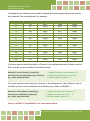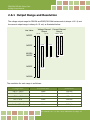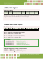
1
PEX/PIO/PISO-DA Series Card User Manual Analog Output Boards Version 3.1, Oct. 2013 SUPPORTS Board includes PIO-DA4, PIO-DA8, PIO-DA16, PIO-DA4U, PIO-DA8U, PIO-DA16U, PISO-DA4U, PISO-DA8U, PISO-DA16U, PEX-DA4, PEX-DA8 and PEX-DA16. WARRANTY All products manufactured by ICP DAS are warranted against defective materials for a period of one year from the date of delivery to the original purchaser. WARNING ICP DAS assumes no liability for damages consequent to the use of this product. ICP DAS reserves the right to change this manual at any time without notice. The information furnished by ICP DAS is believed to be accurate and reliable. However, no responsibility is assumed by ICP DAS for its use, nor for any infringements of patents or other rights of third parties resulting from its use. COPYRIGHT Copyright © 2013 by ICP DAS. All rights are reserved. TRADEMARK Names are used for identification only and may be registered trademarks of their respective companies. CONTACT US If you have any question, please feel to contact us. We will give you quick response within 2 workdays. Email: [email protected], [email protected] PEX/PIO/PISO-DA Series Card Analog Output Boards TABLE OF CONTENTS PACKING LIST ......................................................................................................................................................... 5 RELATED INFORMATION ...................................................................................................................................... 5 1. INTRODUCTION ........................................................................................................................................... 6 1.1 FEATURES .......................................................................................................................................................... 7 1.2 COMPARISON TABLE ........................................................................................................................................... 8 1.3 SPECIFICATIONS ................................................................................................................................................. 9 2. HARDWARE CONFIGURATION ................................................................................................................11 2.1 BOARD LAYOUT ................................................................................................................................................ 11 2.2 COUNTER ARCHITECTURE ................................................................................................................................. 13 2.3 INTERRUPT OPERATION .................................................................................................................................... 14 2.3.1 Interrupt Block Diagram.......................................................................................................................... 15 2.3.2 INT_CHAN_0/1 ......................................................................................................................................... 16 2.3.3 Initial_High, Ative_Low Interrupt Source ............................................................................................. 17 2.3.4 Initial_Low, Ative_High Interrupt Source ............................................................................................. 18 2.3.5 Multiple Interrupt Source ........................................................................................................................ 19 2.4 D/I/O BLOCK DIAGRAM .................................................................................................................................... 21 2.4.1 D/I Port Architecture (CON2) .................................................................................................................. 22 2.4.2 D/O Port Architecture (CON1)................................................................................................................. 23 2.5 D/A ARCHITECTURE ......................................................................................................................................... 24 2.6 D/A CONVERSION OPERATIONS ........................................................................................................................ 25 2.6.1 Output Range and Resolution ................................................................................................................. 27 2.6.2 ± 10 V Voltage Output .............................................................................................................................. 28 2.6.3 ± 5 V Voltage Output ................................................................................................................................ 28 2.6.4 0~10 V Voltage Output ............................................................................................................................ 28 2.6.5 0~5 V Voltage Output .............................................................................................................................. 28 2.6.6 0~20 mA Current Output ........................................................................................................................ 29 2.6.7 4~20 mA Current Output ........................................................................................................................ 29 2.6.8 No VR and No Jumper Design ................................................................................................................ 29 2.6.9 Factory Software Calibration ................................................................................................................... 31 2.6.10 User Software Calibration ................................................................................................................... 33 2.6.11 Voltage Output Connection................................................................................................................. 34 User Manual/ Ver. 3.1/ Oct. 2013/ PMH-0010-31/ Page: 2 PEX/PIO/PISO-DA Series Card Analog Output Boards 2.6.12 Current Output Connection ................................................................................................................ 34 2.7 CARD ID SWITCH .............................................................................................................................................. 35 2.8 PIN ASSIGNMENTS ............................................................................................................................................ 36 3. HARDWARE INSTALLATION ....................................................................................................................37 4. SOFTWARE INSTALLATION......................................................................................................................41 4.1 DRIVER INSTALLING PROCEDURE ...................................................................................................................... 41 4.2 PNP DRIVER INSTALLATION .............................................................................................................................. 43 4.3 CONFIRM THE SUCCESSFUL INSTALLATION ......................................................................................................... 46 5. TESTING PIO-DA CARD .............................................................................................................................47 5.1 SELF-TEST WIRING .......................................................................................................................................... 47 5.1.1 DIO Test Wiring ........................................................................................................................................ 47 5.1.2 Analog Output Test Wiring ...................................................................................................................... 48 5.2 6. EXECUTE THE TEST PROGRAM ........................................................................................................................... 49 I/O CONTROL REGISTER ..........................................................................................................................52 6.1 HOW TO FIND THE I/O ADDRESS ...................................................................................................................... 52 6.1.1 PIO_PISO.EXE Utility for Windows ........................................................................................................ 53 6.1.2 PIO_DriverInit ........................................................................................................................................... 54 6.1.3 PIO_GetConfigAdressSpace .................................................................................................................... 56 6.1.4 Show_PIO_PISO ....................................................................................................................................... 57 6.2 THE ASSIGNMENT OF I/O ADDRESS .................................................................................................................. 58 6.3 THE I/O ADDRESS MAP .................................................................................................................................... 60 6.3.1 RESET\ Control Register .......................................................................................................................... 61 6.3.2 AUX Control Register .................................................................................................................................... 61 6.3.3 Aux Data Register ......................................................................................................................................... 62 6.3.4 INT Mask Control Register........................................................................................................................... 62 6.3.5 Aux Status Register ...................................................................................................................................... 63 6.3.6 Interrupt Polarity Register ........................................................................................................................... 63 6.3.7 Read/Write 8254 Register ............................................................................................................................ 64 6.3.8 Read Card ID Register.................................................................................................................................. 65 6.3.9 Digital Input Register ................................................................................................................................... 66 6.3.10 Digital Output Register .............................................................................................................................. 66 6.3.11 D/A Select Register..................................................................................................................................... 67 6.3.12 D/A Data Output Register ......................................................................................................................... 68 7. DEMO PROGRAM .........................................................................................................................................69 7.1 DEMO PROGRAM FOR WINDOWS ....................................................................................................................... 69 User Manual/ Ver. 3.1/ Oct. 2013/ PMH-0010-31/ Page: 3 PEX/PIO/PISO-DA Series Card Analog Output Boards 7.2 DEMO PROGRAM FOR DOS ............................................................................................................................... 71 APPENDIX: DAUGHTER BOARD .........................................................................................................................73 A1. DB-37 and DN-37 ............................................................................................................................................. 73 A2. DB-8125 ............................................................................................................................................................ 73 A3. DB-16P Isolated Input Board ......................................................................................................................... 74 A5. DB-16R Relay Board ........................................................................................................................................ 75 A6. DB-24PR/DB-24POR/DB-24C Power Relay Board........................................................................................ 76 User Manual/ Ver. 3.1/ Oct. 2013/ PMH-0010-31/ Page: 4 PEX/PIO/PISO-DA Series Card Analog Output Boards Packing List The shipping package includes the following items: One multi-function card as follows: PEX-DA series: PEX-DA4/ PEX-DA8/ PEX-DA16 PIO-DAxU series: PIO-DA4U/ PIO-DA8U/ PIO-DA16U PISO-DAxU series: PISO-DA4U/ PISO-DA8U/ PISO-DA16U One printed Quick Start Guide ★ Note!! One software utility CD One CA-4002 D-Sub Connect If any of these items is missing or damaged, contact the dealer from whom you purchased the product. Save the shipping materials and carton in case you want to ship or store the product in the future. Related Information Product Page: http://www.icpdas.com/root/product/solutions/pc_based_io_board/pci/pio-da4.html Documentation and Software for PIO-DA series classic: CD:\NAPDOS\PCI\PIO-DA\ http://ftp.icpdas.com/pub/cd/iocard/pci/napdos/pci/pio-da/ Documentation and Software for UniDAQ SDK: CD:\NAPDOS\PCI\UniDAQ\ http://ftp.icpdas.com/pub/cd/iocard/pci/napdos/pci/unidaq/ User Manual/ Ver. 3.1/ Oct. 2013/ PMH-0010-31/ Page: 5 PEX/PIO/PISO-DA Series Card Analog Output Boards 1. Introduction The PEX-DA, PISO-DAxU and PIO-DAxU series cards (PCI Express/Universal PCI versions) are compatible with the PIO-DAx cards (PCI versions) and most users can replace the PIO-DAx by PEX-DA, PISO-DAxU or PIO-DAxU directly without software/driver modification. Please refer to user manual (ch 1.1) for the compatibility information. The PISO-DA series adds high-voltage isolation design that offers a durable ability to keep users' computers safe from unexpected surge. It is the built-in high-quality isolation components that make PISO-DA series featuring 2500 VDC bus-typed isolation! For the PEX-DA, PIO-DA and the PISO-DA series, their voltage output range is from -10 V to +10 V, and their current output range is from 0 to 20 mA. In addition, These cards also feature the following advantages by ICP DAS's innovation: 1. Accurate and easy-to-use calibration. ICP DAS provides the software calibration instead of the manual calibration so that no jumpers and trim-pots are required anymore. The calibration information can be saved in EEPROM for long-term use. 2. Individual channel configuration. In other words, every channel can be individually configured as voltage output or current output! 3. Card ID. ICP DAS provides the card ID function for PEX-DA, PISO-DAxU and PIO-DAxU (version 1.1 or above) series. Users can set card ID for each card and then recognize them one by one when more than two boards are used in a computer. Note: This card needs a 12 V power supply, which can be found in either a regular PC or an Industrial PC. User Manual/ Ver. 3.1/ Oct. 2013/ PMH-0010-31/ Page: 6 PEX/PIO/PISO-DA Series Card Analog Output Boards 1.1 Features Supports +5 V PCI bus for PIO-DA4/DA8/DA16 16/8/4 channels, 14-bit analog output Voltage output range: ± 10 V Current output range: 0 ~ 20 mA (sink) Two pacer timer interrupt source Double-buffered D/A latch Software calibration 16-channel DI, 16-channel DO One D-Sub connector, two 20-pin flat cable connectors Connects directly to DB-16P, DB-16R, DB-24C, DB-24PR and DB-24POR [PISO-DA16U/DA8U/DA4U only] Built-in DC/DC converter with 3000 VDC isolation Supports both +5 V and +3.3 V PCI bus 2500 VDC bus-type and power isolation protection Digital input port can be set to pull-high or pull-low Card ID function. [PIO-DA16U/DA8U/DA4U, PEX-DA16/DA8/DA4 only] Supports both +5 V and +3.3 V PCI bus for PIO-DA16U/DA8U/DA4U Supports PCI Express x 1 for PEX-DA16/DA8/DA4 Digital input port can be set to pull-high or pull-low Card ID function User Manual/ Ver. 3.1/ Oct. 2013/ PMH-0010-31/ Page: 7 PEX/PIO/PISO-DA Series Card Analog Output Boards 1.2 Comparison Table Comparison Table of the Different Version Information: Version PIO-DA4 PIO-DA8 - PIO-DA16 PIO-DA4U PIO-DA8U V1.0 PIO-DA16U PIO-DA4U PIO-DA8U V1.1 PIO-DA16U D/I Register Pin Assignment 0xE0/E4/E8/EC A. GND 0xF0/F4/F8/FC (CN3.5/10/15/24/29) 0xE0/E4/E8/EC A. GND 0xF0/F4/F8/FC (CN3.5/10/15/24/29) 0xE0/E4/E8/EC A. GND 0xF0/F4/F8/FC (CN3.5/10/15/24/29) PIO-DA4U PIO-DA8U V1.2 or above 0xE0/E4 V1.3 or above 0xE0/E4 V1.0 0xE0/E4 PIO-DA16U PISO-DA4U PISO-DA8U PISO-DA16U PEX-DA4 PEX-DA8 PEX-DA16 A. GND (CN3.5/10/15) A. GND (CN3.5/10/15/24/29) A. GND (CN3.5/10/15) Card ID N/A N/A Yes Yes Yes Yes User Manual/ Ver. 3.1/ Oct. 2013/ PMH-0010-31/ Page: 8 PEX/PIO/PISO-DA Series Card Analog Output Boards 1.3 Specifications Model Name PEX-DA4/DA8/DA16 PIO-DA4U/DA8U/DA16U PISO-DA4U/DA8U/DA16U Analog Output Isolation N/A Compatibility Resolution Accuracy Output Rang 4/8/16 independent 14-bit 0.04% of FSR ± 2 LSB @ 25 °C, ± 10 V Voltage: +/- 10 V Current: 0 ~ 20 mA ± 5 mA 0.71 V/µs 0.1 Ω max. Software Output Driving Slew Rate Output Impedance Operating Mode N/A 2500 V (Bus Type) Digital Input Channels Compatibility Input Voltage Response Speed 16-ch 5 V/TTL Logic 0: 0.8 V max. Logic 1: 2.0 V min. 200 KHz 1.0 MHz (Typical) Digital Output Channels 16-ch Compatibility Output Logic 0 Voltage Logic 1 Output Sink Capability Source 5 V/CMOS 0.1 V max. 5 V/TTL 0.4 V max. 4.4 V min. 6 mA @ 0.33 V 2.4 V min. 2.4 mA @ 0.8 V 6 mA @ 4.77 V 0.8 mA @ 2.0 V Response Speed 200 KHz 1.0 MHz (Typical) Timer/Counter Channels 3 Resolution 16-bit Compatibility 5 V/TTL Reference Clock Internal: 4 MHz User Manual/ Ver. 3.1/ Oct. 2013/ PMH-0010-31/ Page: 9 PEX/PIO/PISO-DA Series Card Analog Output Boards Model Name PEX-DA4/DA8/DA16 PIO-DA4U/DA8U/DA16U PISO-DA4U/DA8U/DA16U General Bus Type PCI Express x1 Data Bus 8-bit Card ID Yes (4-bit) I/O Connector Dimensions (L x W ) Power Consumption Operating Temperature Storage Temperature Humidity 3.3V/5V Universal PCI, 32-bit, 33MHz Yes (4-bit) for Version 1.1 or above Yes (4-bit) Female DB37 x 1, Male 20-bit ribbon x 2 188 mmx 97 mm 188 mmx 97 mm (Version 1.1 or above) 180 mmx 97 mm 600 mA @ +5 V (PEX-DA4/PIO-DA4U) 2200 mA @ +5 V (PISO-DA4U) 800 mA @ +5 V (PEX-DA8/PIO-DA8U) 2400 mA @ +5 V(PISO-DA8U) 1400 mA @ +5 V (PEX-DA16/PIO-DA16U) 3000 mA @ +5 V(PISO-DA16U) 0 ~ 60 °C -20 ~ 70 °C 5 ~ 85% RH, non-condensing User Manual/ Ver. 3.1/ Oct. 2013/ PMH-0010-31/ Page: 10 PEX/PIO/PISO-DA Series Card Analog Output Boards 2. Hardware Configuration 2.1 Board Layout PIO-DAx Board Layout. CON3 PIO-DA16 PIO-DA8 PIO-DA4 CON2 20 19 DI 2 1 CON1 20 19 DO 2 1 PCI BUS Note: CON1: 16-channel D/O. CON2: 16-channel D/I. CON3: 4/8/16-channel D/A converter voltage/current output. User Manual/ Ver. 3.1/ Oct. 2013/ PMH-0010-31/ Page: 11 PEX/PIO/PISO-DA Series Card Analog Output Boards PIO-DAxU and PISO-DAxU Board Layout. CON3 CON2 2 0 1 9 DI SW1 ON 2 1 1 2 3 4 CON1 2 0 1 9 DO JP1 2 1 Universal PCI BUS PEX-DA Board Layout. CON3 2 0 CON2 1 9 DI SW1 ON 2 1 2 3 4 2 0 1 CON1 1 9 DO JP1 2 1 PCI Express Note: CON1: 16-channel D/O. CON2: 16-channel D/I. CON3: 4/8/16-channel D/A converter voltage/current output. SW1: Card ID. JP1: Pull-high/pull-low resisters for DI. User Manual/ Ver. 3.1/ Oct. 2013/ PMH-0010-31/ Page: 12 PEX/PIO/PISO-DA Series Card Analog Output Boards 2.2 Counter Architecture There is a single 8254(Timer/Counter) chip on the PEX/PIO/PISO-DA series board and provides two interrupt sources. The first is a 16-bit timer output (INT0) and the other one is a 32-bit timer output (INT1). The block diagram is shown below: Vcc 8254 Timer/Counter CLK0 INT0 4MHz OUT0 GATE0 Counter0 CLK1 OUT1 GATE1 Counter1 CLK2 INT1 OUT2 GATE2 Counter2 User Manual/ Ver. 3.1/ Oct. 2013/ PMH-0010-31/ Page: 13 PEX/PIO/PISO-DA Series Card Analog Output Boards 2.3 Interrupt Operation There are two interrupt sources included in the PEX-DA and PIO/PISO-DAxU series. These two signals are named as INT0 and INT1, and their signal sources are as follows: INT0: 8254 counter0 output (Refer to Sec. 2.2) INT1: 8254 counter2 output (Refer to Sec. 2.2) If only one interrupt signal source is used, the interrupt service routine doesn’t have to identify the interrupt source. Refer to DEMO3.C and DEMO4.C for more information. If there is more than one interrupt source, the interrupt service routine has to identify the active signals in the following manner: (Refer to DEMO5.C and DEMO6.C) 1. Read the new status of all interrupt signal sources 2. Compare the new status with the old status to identify the active signals 3. If INT0 is active, service it 4. If INT1 is active, service it 5. Save the new status to replace the old status Note: If the interrupt signal is too short, the new status may be the same as the old status. In that situation, the interrupt service routine will not be able to identify which interrupt source is active, so the interrupt signal must be hold_active for long enough until the interrupt service routine is executed. This hold_time is different for different OS versions. The hold_time can be as short as a micro-second or as long as second. In general, 20 mS should be long enough for all OS version. User Manual/ Ver. 3.1/ Oct. 2013/ PMH-0010-31/ Page: 14 PEX/PIO/PISO-DA Series Card Analog Output Boards 2.3.1 Interrupt Block Diagram INT\ INT_CHAN_0 Level_trigger INT_CHAN_1 (to PEX/PCI slot) initial_low active_high The interrupt output signal of PEX-DA and PIO/PISO-DAxU series cards, INT\, is set to Level-Trigger and Active_Low. If INT\ generates a low_pulse, the PIO-DA4/8/16 will interrupt the PC once each time. If INT\ is fixed at low_level, the PEX-DA and PIO/PISO-DAxU series will interrupt the PC continuously. So for the signal pulse_type for INT_CHAN_0/1 must be controlled and must be fixed at a low_level state normally and a high_pulse generated to interrupt the PC. The priority of INT_CHAN_0/1 is the same. If both of these signals are active at the same time, then INT\ will only be active once at a time. So the interrupt service routine has to read the status of both interrupt channels to per form a multiple-channel interrupt. Refer to Sec. 2.3 for more information. DEMO5.C for INT_CHAN_0 & INT_CHAN_1 If only one interrupt source is used, the interrupt service routine doesn’t have to read the status of the interrupt source. The demo programs, DEMO3.C and DEMO4.C, are designed to demons rate a single channel interrupt. See: DEMO3.C for INT_CHAN_1 only (initial high) DEMO4.C for INT_CHAN_1 only (initial low) User Manual/ Ver. 3.1/ Oct. 2013/ PMH-0010-31/ Page: 15 PEX/PIO/PISO-DA Series Card Analog Output Boards 2.3.2 INT_CHAN_0/1 INT_CHAN_0/1 INT0/1 Inverted/Noninverted select (INV0/1) Enable/Disable select (EN0/1) The architecture for INT_CHAN_0 and INT_CHAN_1 is shown in the above figure. The only difference between INT0 and INT1 is that the INT_CHAN_0 signal source is from the 8254 counter0 output and the INT_CHAN_1 signal source is from the 8254 counter2 output. INT_CHAN_0/1 must be fixed at a low level state normally and a high_pulse generated to interrupt the PC. EN0/1 can be used to enable/disable the INT_CHAN_0/1 in the following manner: (Refer to Sec. 6.3.4) EN0/1 = 0 INT_CHAN_0/1 = disabled EN0/1 = 1 INT_CHAN_0/1 = enabled INV0/1 can be used to invert/non-invert INT0/1 in the following manner: (Refer to Sec. 6.3.5) INV0/1 = 0 INT_CHAN_0/1 = inverted state for INT0/1 INV0/1 = 1 INT_CHAN_0/1 = non-inverted state for INT0/1 As noted above, if INT\ is fixed at a low level state, the PEX-DA and PIO/PISO-DAxU series will interrupt the PC continuously, so the interrupt service routine should use INV0/1 to invert/non-invert the INT0/1 in order to generate a high_pulse (Refer to the next section). User Manual/ Ver. 3.1/ Oct. 2013/ PMH-0010-31/ Page: 16 PEX/PIO/PISO-DA Series Card Analog Output Boards 2.3.3 Initial_High, Ative_Low Interrupt Source If INT0 (8254 counter0 output) is an initial_high, active_low signal (depending on 8254 counter mode), the interrupt service routine should use INV0 to invert/non-invert INT0 to generate a high_pulse in the following manner: (Refer to DEMO3.C) Initial settings: now_int_state=1; outportb(wBase+0x2a,0); /* initial state for INT0 */ /* select the inverted INT0 */ void interrupt irq_service() { if (now_int_state==1) { COUNT_L++; If((inport(wBase+7)&1)==0) { outportb(wBase+0x2a,1); now_int_state=0; } else now_int_state=1; } else { COUNT_H++; If((inport(wBase+7)&1)==1) { outportb(wBase+0x2a,0); now_int_state=1; } else now_int_state=0; /* /* /* /* /* /* /* /* /* now INT0 is changed to LOW --> INT_CHAN_0=!INT0=HIGH now find a LOW_pulse (INT0) the INT0 is still fixed in LOW need to generate a high_pulse INV0 select the non-inverted input INT_CHAN_0=INT0=LOW --> INT_CHAN_0 generate a high_pulse now INT0=LOW /* now INT0=HIGH /* don’t have to generate high_pulse /* /* /* /* /* /* /* /* /* now INT0 is changed to HIGH --> INT_CHAN_0=INT0=HIGH now find a HIGH_pulse (INT0) the INT0 is still fixed in HIGH need to generate a high_pulse INV0 select the inverted input INT_CHAN_0=!INT0=LOW --> INT_CHAN_0 generate a high_pulse now INT0=HIGH /* now INT0=LOW /* don’t have to generate high_pulse } if (wIrq>=8) outportb(A2_8259,0x20); outportb(A1_8259,0x20); } (a) (b) (c) */(a) */ */ */ */ */(b) */ */ */ */ */ */(c) */ */ */ */ */(d) */ */ */ */ */ (d) INT0 INV0 INT_CHAN_0 User Manual/ Ver. 3.1/ Oct. 2013/ PMH-0010-31/ Page: 17 PEX/PIO/PISO-DA Series Card Analog Output Boards 2.3.4 Initial_Low, Ative_High Interrupt Source If INT0 (8254 counter0 output) is an initial_low, active_high signal (depending on the 8254 counter mode), the interrupt service routine should use INV0 to invert/non-invert INT0 to generate a high_pulse in the following manner: (Refer to DEMO4.C) Initial setting: now_int_state=0; outportb(wBase+0x2a,1); /* initial state for INT0 /* select the non-inverted INT0 */ */ void interrupt irq_service() { if (now_int_state==1) /* now INT0 is changed to LOW */(c) { /* --> INT_CHAN_0=!INT0=HIGH now */ COUNT_L++; /* find a LOW_pulse (INT0) */ If((inport(wBase+7)&1)==0)/* the INT0 is still fixed in LOW */ { /* need to generate a high_pulse */ outportb(wBase+0x2a,1); /* INV0 select the non-inverted input */(d) /* INT_CHAN_0=INT0=LOW --> */ /* INT_CHAN_0 generate a high_pulse */ now_int_state=0; /* now INT0=LOW */ } else now_int_state=1; /* now INT0=HIGH */ /* don’t have to generate high_pulse */ } else /* now INT0 is changed to HIGH */(a) { /* --> INT_CHAN_0=INT0=HIGH now */ COUNT_H++; /* find a High_pulse (INT0) */ If((inport(wBase+7)&1)==1)/* the INT0 is still fixed in HIGH */ { /* need to generate a high_pulse */ outportb(wBase+0x2a,0); /* INV0 select the inverted input */(b) /* INT_CHAN_0=!INT0=LOW --> */ /* INT_CHAN_0 generate a high_pulse */ now_int_state=1; /* now INT0=HIGH */ } else now_int_state=0; /* now INT0=LOW */ /* don’t have to generate high_pulse */ } if (wIrq>=8) outportb(A2_8259,0x20); outportb(A1_8259,0x20); } (a) (b) (c) (d) INT0 INV0 INT_CHAN_0 User Manual/ Ver. 3.1/ Oct. 2013/ PMH-0010-31/ Page: 18 PEX/PIO/PISO-DA Series Card Analog Output Boards 2.3.5 Multiple Interrupt Source Assume: INT0 is initial Low and active High, INT1 is initial High and active Low as below: INT0 INT1 INT0 and INT1 are active at the same time INT0 and INT1 return to normal at the same time INT1 returns to normal INT1 is active Refer to DEMO5.C for the source program. All of these falling-edge and rising-edge can be detected using DEMO5.C. Note: When the interrupt is active, the user program has to identify the active signals. These signals may all be active at the same time, so the interrupt service routine has to service all active signals at the same time. User Manual/ Ver. 3.1/ Oct. 2013/ PMH-0010-31/ Page: 19 PEX/PIO/PISO-DA Series Card Analog Output Boards /* ------------------------------------------------------------------------------------------------------- */ /* Note : 1.The hold_time of INT_CHAN_0 & INT_CHAN_1 must long */ /* enoug. */ /* 2.The ISR must read the interrupt status again to */ /* identify the active interrupt source. */ /* 3.The INT_CHAN_0 & INT_CHAN_1 can be active at the same */ /* time. */ /* --------------------------------------------------------------------------------------------------- */ void interrupt irq_service() { /* now ISR can not know which interrupt is active */ new_int_state=inportb(wBase+7)&0x03; /* read all interrupt */ /* signal state */ int_c=new_int_state^now_int_state; /* compare new_state to */ /* old_state */ if ((int_c&0x01)==1) { if ((new_int_state&1)==0) { INT0_L++; } else { INT0_H++; } invert=invert^1; } if ((int_c&0x02)==2) { if ((new_int_state&2)==0) { INT1_L++; } else { INT1_H++; } invert=invert^2; } now_int_state=new_int_state; outportb(wBase+0x2a,invert); /* INT_CHAN_0 is active */ /* INT0 change to low now */ /* INT0 change to high now /* generate high_pulse */ */ /* INT_CHAN_1 is active */ /* INT1 change to low now */ /* INT1 change to high now */ /* generate high_pulse /* update interrupt status /* generate a high pulse */ */ */ if (wIrq>=8) outportb(A2_8259,0x20); outportb(A1_8259,0x20); } User Manual/ Ver. 3.1/ Oct. 2013/ PMH-0010-31/ Page: 20 PEX/PIO/PISO-DA Series Card Analog Output Boards 2.4 D/I/O block Diagram The PEX-DA and PISO/PIO-DAxU series provides 16 digital input channels and 16 digital output channels, and all signal levels are TTL compatible. The connection diagram and block diagram are as follows: CON2 16 bits D/I port 16 bits Local Data Bus CON1 16 bits D/O port 16 bits The D/I Port can be connected to a DB-16P, which is a 16-channel isolated digital input daughter board. The D/O Port can be connected to either a DB-16R or a DB-24PR. The DB-16R is a 16 channels relay output board. The DB-24PR is a 24 channels power relay output board. User Manual/ Ver. 3.1/ Oct. 2013/ PMH-0010-31/ Page: 21 PEX/PIO/PISO-DA Series Card Analog Output Boards 2.4.1 D/I Port Architecture (CON2) When the PC is powered up, all DI port (CON2) operation are disabled. The enabled/disabled status of a DI port is controlled by the RESET\ signal. Refer to Sec. 6.3.1 for more information about the RESET\ signal. The RESET\ signal is in the Low-state all DI operations are disabled The RESET\ signal is in the High-state all DI operations are enabled RESET\ Data disable Buffer input CON2 Clock input D/I buffer CKT User Manual/ Ver. 3.1/ Oct. 2013/ PMH-0010-31/ Page: 22 PEX/PIO/PISO-DA Series Card Analog Output Boards 2.4.2 D/O Port Architecture (CON1) When the PC is powered up, the states of all DO channels are cleared low. The RESET\ signal is used to clear the DO states. Refer to Sec. 6.3.1 for more information about the RESET\ signal. The RESET\ signal is in the Low-state all DO channels are cleared to the low state The block diagram of DO is as follows: RESET\ Data clear input Latch CON1 Clock input D/O buffer CKT User Manual/ Ver. 3.1/ Oct. 2013/ PMH-0010-31/ Page: 23 PEX/PIO/PISO-DA Series Card Analog Output Boards 2.5 D/A Architecture DA_0 D0 d0~d13 DA 1 D13 d14~d15 DA 0 A0 A1 DA 2 Amp DA 3 DA_1 Buffered Data Bus (16 bits) D0 d0~d13 A0 A1 D0 d0~d13 DA 7 DA 8 DA 9 D13 A0 A1 DA10 DA11 DA_3 D0 d0~d13 0 1 2 3 4 5 6 7 8 9 10 11 12 13 14 15 DA12 Amp DA13 D13 d14~d15 Current Output Current Output Current Output Current Output Current Output Current Output Current Output Current Output Current Output Current Output Current Output Current Output Current Output Current Output Current Output Current Output DA 6 DA_2 d14~d15 0 1 2 3 4 5 6 7 8 9 10 11 12 13 14 15 DA 5 D13 d14~d15 DA 4 Voltage Output Voltage Output Voltage Output Voltage Output Voltage Output Voltage Output Voltage Output Voltage Output Voltage Output Voltage Output Voltage Output Voltage Output Voltage Output Voltage Output Voltage Output Voltage Output A0 A1 DA14 DA15 The PEX-DA and PISO/PIO-DAxU provides 4/8/16 channels of double-buffered digital to analog output and provides voltage output and current output simultaneously. User Manual/ Ver. 3.1/ Oct. 2013/ PMH-0010-31/ Page: 24 PEX/PIO/PISO-DA Series Card Analog Output Boards 2.6 D/A Conversion Operations The D/A converters on PEX-DA and PISO/PIO-DAxU series cards use 14-bit resolution, so the digital data values range from 0x0000 to 0x3fff. The hardware is designed to output voltage in a range from -10.1 ~ +10.1 volts, as follows: 0x0000 about –10.1 volts 0x3FFF about +10.1 volts In a conventional design, there will be some VRs that need to be adjusted so that the voltage output for 0x0000 = -10.0 V and 0x3fff = +10.0 V. In addition, these VRs also have to be adjusted so that the current output for 0x1fff = 0 mA and 0x3fff = 20 mA. In conventional designs, these VRs are commonly used for voltage/current output, so the user has to perform some calibration when changing from voltage to current. Also, if these VRs are changed, the user has to re-perform the calibration. This procedure is complex and creates a heavy workload. The PEX-DA and PISO/PIO-DAxU series uses software calibration to replace this complex procedure in the following manner: For each voltage output channel, find two hex values MaxV[n] and MinV[n] (stored in the onboard EEPROM). MaxV[n] is mapped to exactly +10 V and MinV[n] is mapped to exactly –10 V. For each current output channel, also find two hex values MaxI[n] and MinI[n] (stored in the onboard EEPROM). MaxI[n] is mapped to exactly 20 mA and MinI[n] is mapped to exactly 0 mA. MaxV[n] Hex Value Ideal / Actual 0X3FFF +10.1V / +10.?V MaxI[n] +10.0V 20mA DaValue Vout / Iout MinI[n] MinV[n] 0X0000 Calibration 0mA -10.0V -10.1V / -10.?V User Manual/ Ver. 3.1/ Oct. 2013/ PMH-0010-31/ Page: 25 PEX/PIO/PISO-DA Series Card Analog Output Boards Consequently, the software can be used to calibrate the analog output without the need for any hardware Trim-pot adjustment. For example, Channel n 0 1 2 3 4 MinV[n] 134 137 132 134 135 MaxV[n] 16297 16293 16296 16391 16298 MinI[n] 8180 8172 8199 8177 8165 MaxI[n] 15943 15976 15949 15963 15955 5 6 7 8 9 10 11 12 13 14 131 136 134 134 132 135 133 131 134 132 16292 16295 16297 16294 16295 16298 16296 16292 16297 16293 8150 8172 8163 8188 8169 8172 8177 8159 8173 8168 15947 15968 15961 15959 15948 15946 15975 15942 15973 15949 15 133 16295 8175 15965 If the user wants to send Vout(volts) to Channel n, the calibrated hex value, DaValue, sent to D/A converter can be calculated in the following way: DeltaV[n]=20.0/(MaxV[n]–MinV[n]); /* DeltaV[n]=volts per count at channel_n */ DaValue=(Vout+10.0)/DeltaV[n]+MinV[n]; /* DaValue=Hex value to send to the D/A */ pio_da16_da(n,DaValue); /* send the DaValue to Channel n */ If the user wants to send Iout(mA) to Channel n, the calibrated hex value, DaValue, sent to the D/A converter can be calculated in the following way: (Refer to DEMO9.C) DeltaI[n]=20.0/(MaxI[n]–MinI[n]); /* DeltaI[n]=mA per count at channel_n */ DaValue=Iout/DeltaI[n]+MinI[n]; /* DaValue=Hex value send to D/A pio_da16_da(n,DaValue); /* send the DaValue to Channel n */ */ Refer to DEMO7.C and DEMO9.C for more information. User Manual/ Ver. 3.1/ Oct. 2013/ PMH-0010-31/ Page: 26 PEX/PIO/PISO-DA Series Card Analog Output Boards 2.6.1 Output Range and Resolution The voltage output range for PEX-DA and PISO/PIO-DAxU series cards is always ± 10.1 V, and the current output range is always 0~22 mA, as illustrated below: Hex Value 0X3FFF Voltage Channel Output +10.1V +10.1V +5.05V 0X2FFF 0X25D0 0X1FFF 22mA 22mA +5.05V 4mA 0V 0X0FFF 0X0000 Current Channel Output 0V 0mA -5.05V -10.1V The resolution for each range is as follows: Configuration Equivalent Bits Resolution -10 V ~ +10 V 14-bit 1.22 mV 0 V ~ 10 V 13-bit 1.22 mV -5 V ~ +5 V 13-bit 1.22 mV 0 V ~ +5 V 12-bit 1.22 mV 0 mA ~ 20 mA 13-bit 2.70 μA 4 mA ~ 20 mA 13-bit 2.70 μA User Manual/ Ver. 3.1/ Oct. 2013/ PMH-0010-31/ Page: 27 PEX/PIO/PISO-DA Series Card Analog Output Boards 2.6.2 ± 10 V Voltage Output The voltage output for PEX-DA and PISO/PIO-DAxU series cards is always in the range of ± 10.1 V. If the user needs to output a voltage in the range of ± 10 V, the software calibration is the same as that described in Sec. 2.6. Consequently, Vout will be in the range of ± 10 V, so the DaValue will approximately be from 0x0000 to 0x3fff, which means that the resolution is about 14 bits. 2.6.3 ± 5 V Voltage Output The voltage output for PEX-DA and PISO/PIO-DAxU series cards is always in the range of ± 10.1 V. If the user needs to output a voltage in the range of ± 5 V, the software calibration is same as that described in Sec. 2.6. Consequently, Vout will be in range of +5 V, so the DaValue will approximately be from 0x0fff to 0x2fff, which means that the resolution is about 13 bits. 2.6.4 0~10 V Voltage Output The voltage output for PEX-DA and PISO/PIO-DAxU series cards is always in the range of ± 10 V.1. If the user needs to output a voltage in the range of 0~10 V, the software calibration is the same as that described in Sec.2.6. Consequently, Vout will be in the range of 0~10 V, so the DaValue will approximately be from 0x1fff to 0x3fff, which means the resolution is about 13 bits. 2.6.5 0~5 V Voltage Output The voltage output for PEX-DA and PISO/PIO-DAxU series cards is always in the range of 10.1 V. If the user needs to output a voltage in the range of 0~5 V, the software calibration is the same as that described in Sec. 2.6. Consequently, Vout will be in the range 0~5 V, so the DaValue will approximately be from 0x1fff to 0x2fff, which means that the resolution is about 12 bits. User Manual/ Ver. 3.1/ Oct. 2013/ PMH-0010-31/ Page: 28 PEX/PIO/PISO-DA Series Card Analog Output Boards 2.6.6 0~20 mA Current Output The current output for PEX-DA and PISO/PIO-DAxU series cards is always in the range of 0~22 mA. If the user needs to output a current in the range of 0~20 mA, the software calibration is the same as that described in Sec. 2.6. Iout will be in the range of 0~20 mA, so the DaValue will approximately be from 0x1fff to 0x3fff, which means that the resolution is about 13 bits. 2.6.7 4~20 mA Current Output The current output for PEX-DA and PISO/PIO-DAxU series cards is always in the range of 0~22 mA. If the user needs to output a current in the range of 4~20 mA, the software calibration is the same as that described in Sec. 2.6. Iout will be in the range of 4~20 mA, so the DaValue will approximately be from 0x2600 to 0x3fff, which means that the resolution is about 13 bits. 2.6.8 No VR and No Jumper Design In a conventional 12-bit D/A board, for example the A-626/A-628, there are many jumpers that allow the following functions to be performed: (1) Selecting the reference voltage (internal -10/-5/or external) (2) Selecting unipolar/bipolar (0-10 V or 10 V) (3) Selecting different output ranges (0-10 V or 0-5 V) There are also many VRs that allow the following functions to be performed: (1) Adjustment of the output voltage offset (2) Full-scale adjustment of the output voltage (3) Adjustment of the output current offset (4) Full-scale adjustment of the output current User Manual/ Ver. 3.1/ Oct. 2013/ PMH-0010-31/ Page: 29 PEX/PIO/PISO-DA Series Card Analog Output Boards There are so many VRs and jumpers that if makes QC and re-calibration very difficult. Every step must be handled manually, meaning that calibrating these D/A boards is not an enjoyable task. When we designed the PEX-DA and PISO/PIO-DAxU series, we tried to remove many/the these majorities of VRs and jumpers, but still retain the same precision and performance. In the long run, we selected a 14-bit D/A converter and adapted the software calibration to provide at least the same performance and precision as the A-626/A-628: Configuration Equivalent Bits Resolution -10 V ~ +10 V 14-bit 1.22 mV 0 V ~ 10 V 13-bit 1.22 mV -5 V ~ +5 V 13-bit 1.22 mV 0 V ~ +5 V 12-bit 1.22 mV 0 mA ~ 20 mA 13-bit 2.70 μA 4 mA ~ 20 mA 13-bit 2.70 μA All these VRs and jumpers have been removed. All calibrations can be performed using software. All channel configurations can be selected using software, meaning that there is no need to change any hardware. Precision is at least the same as the A-626/A628. All 16 channels can be configured and used in different configurations at the same time. (For example, channel_0=10 V, channel_1=4~20 mA, channel_2=0~5 V, etc) All these features can be implemented on a small, compact and reliable half-size PCB. User Manual/ Ver. 3.1/ Oct. 2013/ PMH-0010-31/ Page: 30 PEX/PIO/PISO-DA Series Card Analog Output Boards 2.6.9 Factory Software Calibration t is recommended that a 16-bit A/D card is used to calibrate the PISO-DA/PIO-DA series cards. The I-7000 series is a set of precise remote control modules and the I-7017 is an 8-channel 16-bit precision A/D module (24-bit sigma-delta A/D converter). Two I-7017 modules are used for voltage output calibration and another two for current output calibration. The steps required to calibrate the voltage for channel_n are as follows: Step 1: DaValue=0 Step 2: Send the DaValue to channel_n on the PIO/PISO card Step 3: Measure the voltage of channel_n on the I-7017 If this value is >= -10 V, then go to Step 5 Step 4: Increase the DaValue, then return to Step 2 Step 5: MinV[n]=DaValue-1 Step 6: DaValue=0x3fff Step 7: Send the DaValue to channel_n on the PIO/PISO card Step 8: Measure the voltage of channel_n on the I-7017 If this value is >= +10 V, then go to Step 10 Step 9: Increase the DaValue, then return to Step 7 Step 10: MaxV[n]=DaValue Note: MinV[n] and MaxV[n] are described in Sec. 2.6 User Manual/ Ver. 3.1/ Oct. 2013/ PMH-0010-31/ Page: 31 PEX/PIO/PISO-DA Series Card Analog Output Boards The steps required to calibrate the current for channel_n are as follows: Step 1: DaValue=0x1fff Step 2: Send the DaValue to hannel_n on the PIO/PISO card Step 3: Measure the current of channel_n on the I-7017 If this value is >= 0 mA, then go to Step 5 Step 4: Increase the DaValue, the return to Step 2 Step 5: MinI[n]=DaValue-1 Step 6: DaValue=0x3fff Step 7: Send the DaValue to channel_n on the PIO/PISO card Step 8: Measure the current of channel_n on the I-7017 If this value is >= 20 mA, than go to Step 10 Step 9: Increase the DaValue, the return to Step 7 Step 10: MaxI[n]=DaValue Note: MinI[n] and MaxI[n] are described in Sec. 2.6 User Manual/ Ver. 3.1/ Oct. 2013/ PMH-0010-31/ Page: 32 PEX/PIO/PISO-DA Series Card Analog Output Boards 2.6.10 User Software Calibration The users can perform calibration themselves using a voltage meter and a current meter. Step 1: Run DEMO12.EXE Step 2: Select the card number for the PEX/PIO/PISO card that you want to calibrate Step 3: Select the item (MinV[n]/MaxV[n]/MinI[n]/MaxI[n]) that you want to calibrate Step 4: Measure the analog output using the voltage meter or the current meter and decide whether to increase or decrease the DaValue. The DaValue will immediately be sent to the D/A converter. The user can then determine the correct value for DaValue that is mapped to the accurate output value. Step 5: Repeat Step 4 for each channel After this procedure, the new data for MinV[n]/MaxV[n]/MinI[n]/MaxI[n] will be stored in the onboard EEPROM. DEMO10.EXE can be executed to back up the old calibration data to “A:\DA16.DAT” before a new calibration is performed. If an error occurs while the new calibration is being performed, DEMO11.EXE can be executed to download the data from “A:\DA16.DAT” to the EEPROM. DEMO10.EXE Save the old calibration data DEMO11.EXE Download the old calibration data DEMO12.EXE Perform a new calibration Note: Demo10.exe, Demo11.exe and Demo12.exe are DOS programs that can run on either a pure DOS or a FreeDOS (http://www.freedos.org/) system. These DOS programs do not work on the DOS command prompt within Windows. User Manual/ Ver. 3.1/ Oct. 2013/ PMH-0010-31/ Page: 33 PEX/PIO/PISO-DA Series Card Analog Output Boards 2.6.11 Voltage Output Connection External Internal Output Current Max (+/- 5mA) D/A Converter Amp V out D0 14-bits Data D13 Load AGND 2.6.12 Current Output Connection External Internal Current Loop 0~20mA + Load - D/A Converter Amp V out D0 14-bits Data External Pow er Supply 9~36V D13 AGND User Manual/ Ver. 3.1/ Oct. 2013/ PMH-0010-31/ Page: 34 PEX/PIO/PISO-DA Series Card Analog Output Boards 2.7 Card ID Switch The PEX-DA , PIO-DAxU (ver. 1.1 or above) and PISO-DAxU has a Card ID switch (SW1) with which users can recognize the board by the ID via software when using two or more PEX-DA , PIO-DAxU (ver. 1.1 or above) and PISO-DAxU series cards in one computer. The default Card ID is 0x0. For detail SW1 Card ID settings, please refer to Table 2.7. NO ID 2 ID 3 ID 1 ID 0 SW1 1 2 3 4 (Default Settings) Table 2.7 (*) Default Settings; OFF 1; ON 0 Card ID (Hex) 1 ID0 2 ID1 3 ID2 4 ID3 (*) 0x0 ON ON ON ON 0x1 OFF ON ON ON 0x2 ON OFF ON ON 0x3 OFF OFF ON ON 0x4 ON ON OFF ON 0x5 OFF ON OFF ON 0x6 ON OFF OFF ON 0x7 OFF OFF OFF ON 0x8 ON ON ON OFF 0x9 OFF ON ON OFF 0xA ON OFF ON OFF 0xB OFF OFF ON OFF 0xC ON ON OFF OFF 0xD OFF ON OFF OFF 0xE ON OFF OFF OFF 0xF OFF OFF OFF OFF User Manual/ Ver. 3.1/ Oct. 2013/ PMH-0010-31/ Page: 35 PEX/PIO/PISO-DA Series Card Analog Output Boards 2.8 Pin Assignments User Manual/ Ver. 3.1/ Oct. 2013/ PMH-0010-31/ Page: 36 PEX/PIO/PISO-DA Series Card Analog Output Boards 3. Hardware Installation Note!! It’s recommended to install driver first, since some operating system (such as Windows 2000) may ask you to restart the computer again after driver installation. This reduces the times to restart the computer. To install your PEX-DAx, PISO-DAxU and PIO-DAxU series card, complete the following steps: Step 1: Installing DAQ card driver on your computer first. For detailed information about the driver installation, please refer to Chapter 4 Software Installation. Step 2: Configuring Card ID by the SW1 DIP-Switch. For detailed information about the card ID (SW1), please refer to Sec. 2.7 Car ID Switch. Note!! The card ID function only supports PEX-DAx, PISO-DAxU and PIO-DAxU (ver.1.1 or above). User Manual/ Ver. 3.1/ Oct. 2013/ PMH-0010-31/ Page: 37 PEX/PIO/PISO-DA Series Card Analog Output Boards Step 3: Shut down and power off your computer. Step 4: Remove all covers from the computer. Step 5: Select an empty PCI/PCI Express slot. User Manual/ Ver. 3.1/ Oct. 2013/ PMH-0010-31/ Page: 38 PEX/PIO/PISO-DA Series Card Analog Output Boards Step 6: Remove the PCI/PCI Express slot cover form the PC. Step 7: Remove the connector cover form the DAQ card. Step 8: Carefully insert your DAQ card into the PCI/PCI Express slot. User Manual/ Ver. 3.1/ Oct. 2013/ PMH-0010-31/ Page: 39 PEX/PIO/PISO-DA Series Card Analog Output Boards Step 9: Tighten the captive Phillips screw. Confirm the PEX-DAx, PISO-DAxU and PIO-DAxU series card is mounted on the motherboard. Step 10: Replace the computer cover. Step 11: Power on the computer. Follow the prompt message to finish the Plug&Play steps, please refer to Chapter 4 Software Installation. User Manual/ Ver. 3.1/ Oct. 2013/ PMH-0010-31/ Page: 40 PEX/PIO/PISO-DA Series Card Analog Output Boards 4. Software Installation The PEX-DAx, PISO-DAxU and PIO-DAxU series card can be used in DOS, Linux and Windows 98/NT/2K and 32-bit/64-bit Windows XP/2003/Vista/7/8. This chapter shows you the detail steps to install these drivers. The recommended installation procedure for Windows is given in Sec. 4.1 ~ 4.3. 4.1 Driver Installing Procedure Follow these steps: Step 1: Run the companion CD. Insert the companion CD into the CD-ROM driver and wait a few seconds until the installation program starts automatically. If it does not start automatically for some reason, then please double-click the file \NAPDOS\AUTO32.EXE on the CD. Step 2: Click the item: PCI Bus DAQ Card. User Manual/ Ver. 3.1/ Oct. 2013/ PMH-0010-31/ Page: 41 PEX/PIO/PISO-DA Series Card Analog Output Boards Step 3: Please install the appropriate driver for your OS. 1. Click the item: “UniDAQ”. 2. Click the item: “DLL for Windows 2000 and XP/2003/Vista 32-bit”. 3. Double-Click “UniDAQ_Win_Setup_x.x.x.x_xxxx.exe” file in the “Driver” folder. User Manual/ Ver. 3.1/ Oct. 2013/ PMH-0010-31/ Page: 42 PEX/PIO/PISO-DA Series Card Analog Output Boards 4. Click the “Next>” button to start the installation. 5. Check your DAQ Card is or not on supported list, Click the “Next>” button. 6. Select the installed folder, the default path is C:\ICPDAS\UniDAQ, confirm and click the “Next>” button. 7. Check your DAQ card on list, then click the “Next>” button. 8. Click the “Next>” button on the Select Additional Tasks window. 9. The demo program can be obtained from the following link and then click the “Next>” button. 10. Select “No, I will restart my computer later” and then click the “Finish” button. For detailed information about the UniDAQ driver installation, please refer to UniDAQ DLL Software Manual. The user manual is contained in: CD:\NAPDOS\PCI\UniDAQ\Manual\ http://ftp.icpdas.com/pub/cd/iocard/pci/napdos/pci/unidaq/manual/ 4.2 PnP Driver Installation Step 1: Turn off the computer and install the DAQ card into the computer. For detailed information about the hardware installation of PEX-DAx, PISO-DAxU and PIO-DAxU series card, please refer to Chapter 3 Hardware Installation. User Manual/ Ver. 3.1/ Oct. 2013/ PMH-0010-31/ Page: 43 PEX/PIO/PISO-DA Series Card Analog Output Boards Step 2: Power on the computer and system should find the new card and then continue to finish the Plug&Play steps. Note: Some Windows OS will load the driver automatically to complete the installation at boot. Step 3: Select “Install the software automatically [Recommended]” and click the “Next>” button. User Manual/ Ver. 3.1/ Oct. 2013/ PMH-0010-31/ Page: 44 PEX/PIO/PISO-DA Series Card Analog Output Boards Step 4: Click the “Finish” button. Step 5: Windows pops up “Found New Hardware” dialog box again. User Manual/ Ver. 3.1/ Oct. 2013/ PMH-0010-31/ Page: 45 PEX/PIO/PISO-DA Series Card Analog Output Boards 4.3 Confirm the Successful Installation Make sure the PEX-DAx, PISO-DAxU and PIO-DAxU series card installed is correct on the computer as follows: Step 1: Select the “Start” “Control Panel” and then double click the “System” icon on Windows. Step 2: Click the “Hardware” tab and then click the “Device Manager” button. Step 3: Check the PEX-DAx, PISO-DAxU and PIO-DAxU series card which listed correctly or not, as illustrated below. User Manual/ Ver. 3.1/ Oct. 2013/ PMH-0010-31/ Page: 46 PEX/PIO/PISO-DA Series Card Analog Output Boards 5. Testing PIO-DA Card This chapter can give you the detail steps about self-test. In this way, user can confirm that PEX-DAx, PISO-DAxU and PIO-DAxU series card well or not. Before the self-test, you must complete the hardware and driver installation. For detailed information about the hardware and driver installation, please refer to Chapter 3 Hardware Installation and Chapter 4 Software Installation. 5.1 Self-Test Wiring 5.1.1 DIO Test Wiring 1. Prepare for device: One CA-2002 (optional) cable. 2. Use the CA-2002 to connect the CON1 with CON2 on board. CON1 CON2 CA-2002 User Manual/ Ver. 3.1/ Oct. 2013/ PMH-0010-31/ Page: 47 PEX/PIO/PISO-DA Series Card Analog Output Boards 5.1.2 Analog Output Test Wiring 1. Prepare for device: One DN-37 (optional) wiring terminal board. One CA-3710 (optional) cable. Digital Multi-Meter. 2. Connect a DN-37 to the CON3. CON3 3. Connect the positive probe (+) of Multi-meter to VO_0 (Pin 0), and then the negative probe (-) of Multi-meter to A.GND (Pin 05). User Manual/ Ver. 3.1/ Oct. 2013/ PMH-0010-31/ Page: 48 PEX/PIO/PISO-DA Series Card Analog Output Boards 5.2 Execute the Test Program 1. Execute the UniDAQ Utility Program. The UniDAQ Utility.exe will be placed in the default path after completing installation. Default Path: C:\ICPDAS\UniDAQ\Driver\ Double click the “UniDAQUtility.exe” Double-Click 1 Click this button to start test. 3 2 Confirm the PIO-DA series card had successfully installed to PC. It starts from 0. Note!! The PEX-DAx software is fully compatible with the PIO-DAxU series software. User Manual/ Ver. 3.1/ Oct. 2013/ PMH-0010-31/ Page: 49 PEX/PIO/PISO-DA Series Card Analog Output Boards 2. Get Digital Output/Input Function test result. Click “Digital Output” item. 4 6 Check channel 0, 2, 4, 6 Select the “Port 0” 5 Click “Digital Input” item. 7 9 The corresponding D/I becomes red for channel 0, 2, 4, 6 of D/O is ON. Select the “Port 0” 8 PASS User Manual/ Ver. 3.1/ Oct. 2013/ PMH-0010-31/ Page: 50 PEX/PIO/PISO-DA Series Card Analog Output Boards 3. Get Analog Output Function test result. Click “Analog Output” item. 14 Click this button. 18 15 Select the “Channel 0” 16 Select the “+/- 10V” 17 Type the voltage value The value read on meter may be a little difference from the DA value because of the resolution limit of meter or the measurement error. 4.995 PASS 19 Check the value on multi-meter, they should be identical to the values set in program. User Manual/ Ver. 3.1/ Oct. 2013/ PMH-0010-31/ Page: 51 PEX/PIO/PISO-DA Series Card Analog Output Boards 6. I/O Control Register 6.1 How to Find the I/O Address The plug&play BIOS will assign a proper I/O address to every PIO/PISO series card in the power-on stage. The fixed IDs for the PEX-DAx, PISO-DAxU and PIO-DAxU series card are given as follows: Table 6-1: Version PIO-DA4 PIO-DA4 PIO-DA4U PISO-DA4U PEX-DA4 PIO-DA8 PIO-DA8 PIO-DA8U PISO-DA8U PEX-DA8 PIO-DA16 PIO-DA16 PIO-DA16U PISO-DA16U PEX-DA16 1.0 ~ 4.0 ~ 1.0 ~ 1.0 ~ 1.0 ~ 1.0 ~ 3.0 above above above above above Vendor ID 0xE159 0xE159 0xE159 0xE159 0xE159 0xE159 Device ID 0x02 0x01 0x01 0x01 0x01 0x01 0x80 0x4180 0x4180 0x4180 0x4180 0x4180 0x04 0x00 0x00 0x00 0x00 0x00 0x00 0x00 0x00 0x00 0x00 0x00 Sub Vendor ID Sub Device ID Sub-Axu ID User Manual/ Ver. 3.1/ Oct. 2013/ PMH-0010-31/ Page: 52 PEX/PIO/PISO-DA Series Card Analog Output Boards 6.1.1 PIO_PISO.EXE Utility for Windows The PIO_PISO.EXE utility program will detect and present all information for ICPDAS I/O cards installed in the PC, as shown in the following Figure6-1. Details of how to identify the PEX-DAx, PISO-DAxU and PIO-DAxU series card of ICPDAS data acquisition boards based on the Sub-vendor, Sub-device and Sub-Aux ID are given in Table 6-1. The PIO_PISO.exe utility is located on the CD as below and is useful for all PIO/PISO series cards. (CD:\NAPDOS\PCI\Utility\Win32\PIO_PISO\) http://ftp.icpdas.com/pub/cd/iocard/pci/napdos/pci/utility/win32/pio_piso/ Figure 6-1 User Manual/ Ver. 3.1/ Oct. 2013/ PMH-0010-31/ Page: 53 PEX/PIO/PISO-DA Series Card Analog Output Boards ICP DAS provides the following necessary functions: 1. PIO_DriverInit(&wBoard, wSubVendor, wSubDevice, wSubAux) 2. PIO_GetConfigAddressSpace(wBoardNo,*wBase,*wIrq, *wSubVendor, *wSubDevice, *wSubAux, *wSlotBus, *wSlotDevice) 3. Show_PIO_PISO(wSubVendor, wSubDevice, wSubAux) 6.1.2 PIO_DriverInit PIO_DriverInit(&wBoards, wSubVendor,wSubDevice,wSubAux) wBoards=0 to N The number of boards found in this PC wSubVendor The subVendor ID of the board you are seeking wSubDevice The subDevice ID of the board your are seeking wSubAux The subAux ID of the board you are seeking This function can be used to detect all PIO/PISO series cards within your system. Implementation is based on the PCI Plug&Play mechanism. The function locates all PIO/PISO series cards installed in this system and save the relevant resource information in the library. Sample program 1: Detect all PEX/PISO/PIO-DA series cards installed in this PC. /* Step 1: Detect all PEX/PISO/PIO-DAx series cards installed in this PC */ wSubVendor=0x80; wSubDevice=4; wSubAux=0x00; /* For PIO-DA4/8/16 series cards*/ wRetVal=PIO_DriverInit(&wBoards, wSubVendor,wSubDevice,wSubAux); printf("There are %d PIO-DA16 Cards in this PC\n",wBoards); /* Step 2: Save the resource information for all PIO-DA4/8/16 series cards installed in this PC */ for (i=0; i<wBoards; i++) { PIO_GetConfigAddressSpace(i,&wBase,&wIrq,&wID1,&wID2,&wID3,&wID4,&wID5); printf("\nCard_%d: wBase=%x, wIrq=%x", i,wBase,wIrq); wConfigSpace[i][0]=wBaseAddress; wConfigSpace[i][1]=wIrq; /*Save the resource information for this card */ /*Save the resource information for this card */ } User Manual/ Ver. 3.1/ Oct. 2013/ PMH-0010-31/ Page: 54 PEX/PIO/PISO-DA Series Card Analog Output Boards Sample program 2: Detect all PIO/PISO cards installed in this PC. /* Step 1: Detect all PIO/PISO series cards installed in this PC */ wRetVal=PIO_DriverInit(&wBoards,0xff,0xff,0xff); /* Detect all PIO_PISO series cards */ printf("\nThere are %d PIO_PISO Cards in this PC",wBoards); if (wBoards==0 ) exit(0); /* Step 2: Save the resource information for all PIO/PISO cards installed in this PC */ printf("\n-----------------------------------------------------"); for(i=0; i<wBoards; i++) { PIO_GetConfigAddressSpace(i,&wBase,&wIrq,&wSubVendor, &wSubDevice,&wSubAux,&wSlotBus,&wSlotDevice); printf("\nCard_%d:wBase=%x,wIrq=%x,subID=[%x,%x,%x], SlotID=[%x,%x]",i,wBase,wIrq,wSubVendor,wSubDevice, wSubAux,wSlotBus,wSlotDevice); printf(" --> "); ShowPioPiso(wSubVendor,wSubDevice,wSubAux); } User Manual/ Ver. 3.1/ Oct. 2013/ PMH-0010-31/ Page: 55 PEX/PIO/PISO-DA Series Card Analog Output Boards 6.1.3 PIO_GetConfigAdressSpace PIO_GetConfigAddressSpace(wBoardNo,*wBase,*wIrq, *wSubVendor,*wSubDevice,*wSubAux,*wSlotBus, *wSlotDevice) wBoards=0 to N The total number of boards using the PIO_DriverInit(...) function wBase The base address of the board control word wIrq The allocated IRQ channel number for this board wSubVendor The subVendor ID of this board wSubDevice The subDevice ID of this board wSubAux The subAux ID of this board wSlotBus The bus number of the slot used by this board wSlotDevice The device number of the slot used by this board The function can be used to save the resource information for all PIO/PISO cards installed in this system. The application program can then directly control all functions of the PIO/PISO series card. Detect the configuration address space for your PEX/PISO/PIO-DA series cards. /* Step 1: Detect all PEX/PISO/PIO-DA series cards */ wSubVendor=0x80; wSubDevice=4; wSubAux=0x00; /*For PIO_DA4/8/16 series cards */ wRetVal=PIO_DriverInit(&wBoards, wSubVendor,wSubDevice,wSubAux); printf("There are %d PIO-DA16/8/4 Cards in this PC\n",wBoards); /* Step 2: Save the resource information for all PEX/PISO/PIO-DA cards installed in this PC */ for (i=0; i<wBoards; i++) { PIO_GetConfigAddressSpace(i,&wBase,&wIrq,&t1,&t2,&t3,&t4,&t5); printf("\nCard_%d: wBase=%x, wIrq=%x", i,wBase,wIrq); wConfigSpace[i][0]=wBaseAddress; /*Save the resource information for this card*/ wConfigSpace[i][1]=wIrq; /*Save the resource information for this card*/ } /* Step 3: Control the PEX/PISO/PIO cards directly */ wBase=wConfigSpace[0][0]; /* get the base address for card_0 */ outport(wBase,1); /* enable all D/I/O operations of card_0 */ wBase=wConfigSpace[1][0]; outport(wBase,1); /* get the base address for card_1 */ /* enable all D/I/O operations of card_1 */ User Manual/ Ver. 3.1/ Oct. 2013/ PMH-0010-31/ Page: 56 PEX/PIO/PISO-DA Series Card Analog Output Boards 6.1.4 Show_PIO_PISO Show_PIO_PISO(wSubVendor,wSubDevice,wSubAux) wSubVendor The subVendor ID of the board you are seeking wSubDevice The subDevice ID of the board you are seeking wSubAux The subAux ID of the board you are seeking This function will display a text string showing these special subIDs, which are the same as those defined in the PIO.H include file. The code for the demo program is as follows: /* Detect all PIO_PISO series cards installed in this PC */ wRetVal=PIO_DriverInit(&wBoards,0xff,0xff,0xff); printf("\nThere are %d PIO_PISO Cards in this PC",wBoards); if (wBoards==0 ) exit(0); printf("\n-----------------------------------------------------"); for(i=0; i<wBoards; i++) { PIO_GetConfigAddressSpace(i,&wBase,&wIrq,&wSubVendor, &wSubDevice,&wSubAux,&wSlotBus,&wSlotDevice); printf("\nCard_%d:wBase=%x,wIrq=%x,subID=[%x,%x,%x], SlotID=[%x,%x]",i,wBase,wIrq,wSubVendor,wSubDevice, wSubAux,wSlotBus,wSlotDevice); printf(" --> "); ShowPioPiso(wSubVendor,wSubDevice,wSubAux); } User Manual/ Ver. 3.1/ Oct. 2013/ PMH-0010-31/ Page: 57 PEX/PIO/PISO-DA Series Card Analog Output Boards 6.2 The Assignment of I/O Address The plug&play BIOS will assign the proper I/O address to PEX-DAx, PISO-DAxU and PIO-DAxU series card. If there is only one PEX-DAx, PISO-DAxU and PIO-DAxU series card, the user can identify the board_0. If there are two PEX-DAx, PISO-DAxU and PIO-DAxU series cards in the system, the user will be very difficult to identify which board is board_0. The software driver can support 16 boards max. Therefore the user can install 16 boards in one PC system. Sometimes, it is difficult to find the card number. The easiest way to identify which card is card_0 is to use the wSlotBus and wSlotDevice functions in the following manner: Step 1: Remove all PEX/PISO/PIO-DA series cards from the PC. Step 2: Install a PEX/PISO/PIO-DA series card into PCI_slot1 on the PC and then run PIO_PISO.EXE. Record the results shown for wSlotBus1 and wSlotDevice1. Step 3: Remove all PEX/PISO/PIO-DA series cards from the PC. Step 4: Install a PEX/PISO/PIO-DA series card into PCI_slot2 on the PC and then run PIO_PISO.EXE again. Record the result shown for wSlotBus2 and wSlotDevice2. Step 5: Repeat (3) and (4) for all PCI_slots and record the results shown for each wSlotBus and wSlotDevice. User Manual/ Ver. 3.1/ Oct. 2013/ PMH-0010-31/ Page: 58 PEX/PIO/PISO-DA Series Card Analog Output Boards A possible sample record: Table 6-2: PC’s PCI slot wSlotBus wSlotDevice Slot_1 0 0x07 Slot_2 0 0x08 Slot_3 0 0x09 Slot_4 0 0x0A Slot_5 1 0x0A Slot_6 1 0x08 Slot_7 1 0x09 Slot_8 1 0x07 PCI-BRIDGE The procedure outlined above can be used to record all wSlotBus and wSlotDevice information for all slots in the PC. This mapping is fixed for each PC, and can then be used to identify a specific PIO-PISO card in the following manner: Step 1: Record all wSlotBus and wSlotDevice information. Step 2: Use the PIO_GetConfigAddressSpace(…) function to retrieve the wSlotBus and wSlotDevice information for the specified card. Step 3: The specified PIO-PISO card can be identified from the two results. User Manual/ Ver. 3.1/ Oct. 2013/ PMH-0010-31/ Page: 59 PEX/PIO/PISO-DA Series Card Analog Output Boards 6.3 The I/O Address Map The I/O address for PEX-DAx, PISO-DAxU and PIO-DAxU series cards is automatically assigned by the ROM BIOS of the PC and provides Plug&Play capabilities for PIO/PISO series cards. The PEX-DAx, PISO-DAxU and PIO-DAxU series I/O addresses are mapped as follows: Table 6-3: Refer to Sec. 6.1.3 for more information about wBase. Address Read Write wBase+0 Reserved RESET\ control register wBase+2 Reserved Aux control register wBase+3 Aux data register Aux data register wBase+5 Reserved INT mask control register wBase+7 Aux pin status register Same wBase+0x2a Reserved INT polarity control register wBase+0xc0 Read 8254-Counter0 Write 8254-Counter0 wBase+0xc4 Read 8254-Counter1 Write 8254-Counter1 wBase+0xc8 Read 8254-Counter2 Write 8254-Counter2 wBase+0xcc Read 8254 control word Write 8254 control word wBase+0xd4 Read the Card ID Reserved wBase+0xe0 Read the Low byte of D/I DA_0 chip select wBase+0xe4 Read the High byte of D/I Read the Low byte of D/I DA_1 chip select wbase+0xe8 wBase+0xec wBase+0xf0 wBase+0xf4 wBase+0xf8 wBase+0xfc (for PEX/PIO-DA only) Read the High byte of D/I (for PEX/PIO-DA only) Read the Low byte of D/I (for PEX/PIO-DA only) Read the High byte of D/I (for PEX/PIO-DA only) Read the Low byte of D/I (for PEX/PIO-DA only) Read the High byte of D/I (for PEX/PIO-DA only) DA_2 chip select DA_3 chip select Write the Low byte of D/A Write the High byte of D/A Write the Low byte of D/O Write the High byte of D/O User Manual/ Ver. 3.1/ Oct. 2013/ PMH-0010-31/ Page: 60 PEX/PIO/PISO-DA Series Card Analog Output Boards 6.3.1 RESET\ Control Register (Write): wBase+0 Bit 7 Bit 6 Bit 5 Bit 4 Bit 3 Bit 2 Bit 1 Bit 0 Reserved Reserved Reserved Reserved Reserved Reserved Reserved RESET\ When the PC’s power is first turned on, RESET\ signal is in a Low-state. This will disable all DI/DO operations. The user has to set the RESET\ signal to a High-state before any DI/DO command applications are initiated. For example: outportb (wBase,1); outportb (wBase,0); /* RESET\=High all D/I/O are enable now */ /* RESET\=Low all D/I/O are disable now */ 6.3.2 AUX Control Register (Read/Write): wBase+2 Bit 7 Bit 6 Bit 5 Bit 4 Bit 3 Bit 2 Bit 1 Bit 0 Aux7 Aux6 Aux5 Aux4 Aux3 Aux2 Aux1 Aux0 Aux?=0 this Aux is used as a D/I Aux?=1 this Aux is used as a D/O When the PC is first turned on, all Aux signals are in a Low-state. All Aux are designed as D/I for all PIO/PISO series. Please set all Aux to the DI state. User Manual/ Ver. 3.1/ Oct. 2013/ PMH-0010-31/ Page: 61 PEX/PIO/PISO-DA Series Card Analog Output Boards 6.3.3 Aux Data Register (Read/Write): wBase+3 Bit 7 Bit 6 Bit 5 Bit 4 Bit 3 Bit 2 Bit 1 Bit 0 Aux7 Aux6 Aux5 Aux4 Aux3 Aux2 Aux1 Aux0 When the Aux is used for D/O, the output state is controlled by this register. This register is designed for feature extension. Therefore, do not use this register. 6.3.4 INT Mask Control Register (Read/Write): wBase+5 Bit 7 Bit 6 Bit 5 Bit 4 Bit 3 Bit 2 Bit 1 Bit 0 0 0 0 0 0 0 EN1 EN0 EN0=0 Disable INT0 as an interrupt signal (Default). EN0=1 Enable INT0 as an interrupt signal EN1=0 Disable INT1 as an interrupt signal (Default) EN1=1 Enable INT1 as an interrupt signal For example: outportb(wBase+5,0); outportb(wBase+5,1); outportb(wBase+5,2); outportb(wBase+5,3); /*Disable all interrupt */ /* Enable interrupt of INT0 */ /* Enable interrupt of INT1 */ /* Enable both interrupt channels */ Refer to the following demo programs for more information: DEMO3.C and DEMO4.C single interrupt source DEMO5.C and DEMO6.C multiple interrupt source User Manual/ Ver. 3.1/ Oct. 2013/ PMH-0010-31/ Page: 62 PEX/PIO/PISO-DA Series Card Analog Output Boards 6.3.5 Aux Status Register (Read/Write): wBase+7 Bit 7 Bit 6 Bit 5 Bit 4 Bit 3 Bit 2 Bit 1 Bit 0 Aux7 Aux6 Aux5 Aux4 Aux3 Aux2 Aux1 Aux0 Aux0=INT0, Aux1=INT1, Aux2~3= EEPROM control, Aux4~7=Aux-ID. Refer to Sec. 4.1 for more information. Aux0~1 are used as interrupt sources. The interrupt service routine needs to read this register to identify the interrupt sources. Refer to Sec. 2.3 for more information. 6.3.6 Interrupt Polarity Register (Read/Write): wBase+0x2A Bit 7 Bit 6 Bit 5 Bit 4 Bit 3 Bit 2 Bit 1 Bit 0 0 0 0 0 0 0 INV1 INV0 INV0/1=0 select the inverted signal from INT0/1 INV0/1=1 select the non-inverted signal from INT0/1 For example: outportb(wBase+0x2a,0); outportb(wBase+0x2a,3); outportb(wBase+0x2a,2); /*Select the inverted input from both channels */ /*Select the non-inverted input from both channels */ /*Select the inverted input from INT0 */ /*Select the non-inverted input from the others */ Refer to Sec. 2.3 and the DEMO3/4/5/6.C files for more information. User Manual/ Ver. 3.1/ Oct. 2013/ PMH-0010-31/ Page: 63 PEX/PIO/PISO-DA Series Card Analog Output Boards 6.3.7 Read/Write 8254 Register (Read/Write): (Read/Write): (Read/Write): (Read/Write): wBase+0xc0=8254-counter-0 wBase+0xc4=8254-counter-1 wBase+0xc8=8254-counter-2 wBase+0xcc=8254 control word 8254 Control Word SC1 SC0 RL1 RL0 M2 M1 M0 BCD [SC1, SC0]: 00: counter0 01: counter1 10: counter2 11: read-back command [RL1, RL0]: 00: counter latch instruction 01: read/write low counter byte only 10: read/write high counter byte only 11: read/write low counter byte first, then high counter byte [M2, M1, M0]: 000: mode0 interrupt on terminal count 001: mode1 programmable one-shot 010: mode2 011: mode3 100: mode4 101: mode5 rate generator square-wave generator software-triggered pulse hardware-triggered pulse [BCD]: 0: binary count 1: BCD count User Manual/ Ver. 3.1/ Oct. 2013/ PMH-0010-31/ Page: 64 PEX/PIO/PISO-DA Series Card Analog Output Boards For example: WORD pio_da16_c0(char cConfig, char cLow, char cHigh) /*COUNTER_0*/ { outportb(wBase+0xcc,cConfig); outportb(wBase+0xc0,cLow); outportb(wBase+0xc0,cHigh); return(NoError); } WORD pio_da16_c1(char cConfig, char cLow, char cHigh) /*COUNTER_1*/ { outportb(wBase+0xcc,cConfig); outportb(wBase+0xc4,cLow); outportb(wBase+0xc4,cHigh); return(NoError); } WORD pio_da16_c2(char cConfig, char cLow, char cHigh) /*COUNTER_2*/ { outportb(wBase+0xcc,cConfig); outportb(wBase+0xc8,cLow); outportb(wBase+0xc8,cHigh); return(NoError); } 6.3.8 Read Card ID Register (Read): wBase+0xd4 Bit 7 Bit 6 Bit 5 Bit 4 Bit 3 Bit 2 Bit 1 Bit 0 0 0 0 0 ID3 ID2 ID1 ID0 For example: wCardID = inportb(wBase+0xd4); /* read Card ID(0x0~0x15) */ Note: The Card ID function is only supported by the PEX-DA, PISO-DAxU and PIO-DAxU(Ver. 1.1 or above) User Manual/ Ver. 3.1/ Oct. 2013/ PMH-0010-31/ Page: 65 PEX/PIO/PISO-DA Series Card Analog Output Boards 6.3.9 Digital Input Register (Read): wBase+0xe0 Low byte of the D/I port Bit 7 Bit 6 Bit 5 Bit 4 Bit 3 Bit 2 Bit 1 Bit 0 DI7 DI6 DI5 DI4 DI3 DI2 DI1 DI0 (Read): wBase+0xe4 High byte of the D/I port Bit 7 Bit 6 Bit 5 Bit 4 Bit 3 Bit 2 Bit 1 Bit 0 DI15 DI14 DI13 DI12 DI11 DI10 DI9 DI8 For example: wDiLoByte = inportb(wBase+0xe0); wDiHiByte = inportb(wBase+0xe4); wDiValue = (wDiHiByte<<8)|wDiLoByte; /* Read the D/I state (DI7~DI0) */ /* Read the D/I state (DI15~DI8) */ Refer to the DEMO2.C file for more information. 6.3.10 Digital Output Register (Write): wBase+0xf8 Low byte of the D/O port Bit 7 Bit 6 Bit 5 Bit 4 Bit 3 Bit 2 Bit 1 Bit 0 DO7 DO6 DO5 DO4 DO3 DO2 DO1 DO0 (Write): wBase+0xfc High byte of the D/O port Bit 7 Bit 6 Bit 5 Bit 4 Bit 3 Bit 2 Bit 1 Bit 0 DO15 DO14 DO13 DO12 DO11 DO10 DO9 DO8 For example: outportb(wBase+0xf8,wDoValue); outportb(wBase+0xfc,wDoValue>>8); /*Controls the DO state (DO7~DO0) */ /*Controls the DO state (DO15~DO8) */ Refer to the DEMO1/2.C file for more information. User Manual/ Ver. 3.1/ Oct. 2013/ PMH-0010-31/ Page: 66 PEX/PIO/PISO-DA Series Card Analog Output Boards 6.3.11 D/A Select Register There are 1/2/4 D/A converters in PEX/PISO/PIO-DA series cards. It is necessary to select which D/A converter is desired after the D/A data has be sent. D/A channels are allocated as follows: Write wBase+0xe0 DA_0 wbase+0xe4 DA_1 wbase+0xe8 DA_2 wbase+0xec DA_3 A1 0 0 1 1 0 0 1 1 0 0 1 1 0 0 1 1 A0 0 1 0 1 0 1 0 1 0 1 0 1 0 1 0 1 Description D/A output channel 0 D/A output channel 1 D/A output channel 2 D/A output channel 3 D/A output channel 4 D/A output channel 5 D/A output channel 6 D/A output channel 7 D/A output channel 8 D/A output channel 9 D/A output channel10 D/A output channel11 D/A output channel12 D/A output channel13 D/A output channel14 D/A output channel15 For example: outportb(wBase+0xf0,wDaValue); /* output the low byte for D/A data */ outportb(wBase+0xf4,(wDaValue>>8)|0x02); /*output the high byte for D/A data and*/ /*select channel 2 on this converter*/ outportb(wBase+0xe0,0); /*select DA_0*/ /* after this procedure, the wDaValue will */ /* be sent to channel_2 */ Refer to the DEMO6.C, DEMO7.C, DEMO8.C and DEMO9.C files for more information. User Manual/ Ver. 3.1/ Oct. 2013/ PMH-0010-31/ Page: 67 PEX/PIO/PISO-DA Series Card Analog Output Boards 6.3.12 D/A Data Output Register (Write): wBase+0xf0 Bit 7 Bit 6 Bit 5 Bit 4 Bit 3 Bit 2 Bit 1 Bit 0 D7 D6 D5 D4 D3 D2 D1 D0 (Write): wBase+0xf4 Bit 7 Bit 6 Bit 5 Bit 4 Bit 3 Bit 2 Bit 1 Bit 0 A1 A0 D13 D12 D11 D10 D9 D8 Each D/A converter have four analog output channels. When writing data to the D/A converter, the relevant channel to be used is indicated by A1 and A0. D/A programming sequence: 1. Send data to the D/A converter. (This data will be buffered) 2. Select the D/A converter. (Start the conversion) For example: outportb(wBase+0xf0,wDaValue); /* output low byte of D/A data*/ outportb(wBase+0xf4,(wDaValue>>8)|0x02); /* output high byte of D/A data and */ /* select channel 2 on this converter */ outportb(wBase+0xe0,0); /* select DA_0 */ /* after this procedure wDaValue will */ /* be sent to channel_2 */ pio_da16_da(2,wDaValue); /* send wDaValue to channel_2 */ void pio_da16_da(char cChannel_no,int iVal) { iVal=iVal+(cChannel_no%4)*0x4000; /* cChannel_no: 0 - 15 */ outportb(wBase+0xf0,iVal); /* iVal: 0x0000 - 0x3fff */ outportb(wBase+0xf4,(iVal>>8)); outportb(wBase+0xe0+4*(cChannel_no/4),0xff); } Refer to the DEMO6/7/8/9.C files for more information. User Manual/ Ver. 3.1/ Oct. 2013/ PMH-0010-31/ Page: 68 PEX/PIO/PISO-DA Series Card Analog Output Boards 7. Demo Program 7.1 Demo Program for Windows All demo programs will not work properly if the DLL driver has not been installed correctly. During the DLL driver installation process , the install-shields will register the correct kernel driver to the operation system and copy the DLL driver and demo programs to the correct position based on the driver software package you have selected (Win98/Me/NT/2K and 32-/64-bit winXP/2003/Vista/7/8). Once driver installation is complete, the related demo programs and development library and declaration header files for different development environments will be presented as follows. Demo Program for PIO-DA Series Classic Driver: The demo program of PIO-DA series is contained in: CD:\NAPDOS\PCI\PIO-DA\DLL_OCX\Demo\ http://ftp.icpdas.com/pub/cd/iocard/pci/napdos/pci/pio-da/dll_ocx/demo/ There are about demo program given as follows: Includes the BCB, Csharp, Delphi, VB.net, VC.net, VB and VC demo programs with source code. DA demo: D/A Output demo DIO demo: D/I/O demo DIO2 demo: D/I/O LED interface Interrupt demo: Single interrupt For detailed information about the DLL function of the PIO-DA series, please refer to DLL Software Manual (CD:\NAPDOS\PCI\PIO-DA\Manual\) User Manual/ Ver. 3.1/ Oct. 2013/ PMH-0010-31/ Page: 69 PEX/PIO/PISO-DA Series Card Analog Output Boards Demo Program for UniDAQ SDK Driver The demo program is contained in: CD:\NAPDOS\PCI\UniDAQ\DLL\Demo\ http://ftp.icpdas.com/pub/cd/iocard/pci/napdos/pci/unidaq/dll/demo/ There are about demo program given as follows: Includes the BCB, Delphi, VB.net, VC.net, VB and VC demo programs with source code. Analog Input Pacer Analog Input Pacer Continue Analog Input Pacer Scan Analog Input Pacer Scan Continue Analog Input Pacer Scan EXT Analog Input Polling Analog Output Analog Output Current Digital I/O Digital I/O by Card ID For detailed information about the DLL function and demo program of the UniDAQ, please refer to UniDAQ DLL Software Manual (CD:\NAPDOS\PCI\UniDAQ\Manual\) User Manual/ Ver. 3.1/ Oct. 2013/ PMH-0010-31/ Page: 70 PEX/PIO/PISO-DA Series Card Analog Output Boards 7.2 Demo Program for DOS The related DOS software and demos are located on the CD as below: CD:\NAPDOS\PCI\PIO-DA\dos\ http://ftp.icpdas.com/pub/cd/iocard/pci/napdos/pci/pio-da/dos/ After installing the software, the following drivers will be installed onto your hard disk: \TC\*.* for Turbo C 2.xx or above \TC\LIB\*.* for TC library \TC\DEMO\*.* for TC demo programs \TC\LIB\Large\*.* TC large model library \TC\LIB\Huge\*.* TC huge model library \TC\LIB\Large\PIO.H TC declaration file \TC\\LIB\Large\TCPIO_L.LIB TC large model library file \TC\LIB\Huge\PIO.H \TC\\LIB\Huge\TCPIO_H.LIB TC declaration file TC huge model library file \MSC\*.* for MSC 5.xx or above \MSC\LIB\Large\PIO.H MSC declaration file \MSC\LIB\Large\MSCPIO_L.LIB MSC large model library file \MSC\LIB\Huge\PIO.H MSC declaration file \MSC\\LIB\Huge\MSCPIO_H.LIB MSC huge model library file \BC\*.* for BC 3.xx or above \BC\LIB\Large\PIO.H \BC\LIB\Large\BCPIO_L.LIB \BC\LIB\Huge\PIO.H BC declaration file BC large model library file BC declaration file \BC\\LIB\Huge\BCPIO_H.LIB BC huge model library file Note: The library is valid for all PIO/PISO series cards. User Manual/ Ver. 3.1/ Oct. 2013/ PMH-0010-31/ Page: 71 PEX/PIO/PISO-DA Series Card Analog Output Boards There are about demo program given as follows: DEMO1.EXE: DEMO2.EXE: DEMO3.EXE: DEMO4.EXE: DEMO5.EXE: DEMO6.EXE: DEMO7.EXE: Waveform generator with calibration DEMO8.EXE: D/A hex value output without calibration DEMO9.EXE: D/A hex value output with calibration DEMO10.EXE: Save EEPROM data to file DEMO11.EXE: Download EEPROM data from file DEMO12.EXE: User software calibration DEMO13.EXE: Factory calibration D/O demo program D/I/O demo program Single interrupt source (initial high) Single interrupt source (initial low) Two interrupt source Waveform generator without calibration Note: The calibration demos programs can only be used in a DOS system. User Manual/ Ver. 3.1/ Oct. 2013/ PMH-0010-31/ Page: 72 PEX/PIO/PISO-DA Series Card Analog Output Boards Appendix: Daughter Board A1. DB-37 and DN-37 DB-37: The DB-37 is a general purpose daughter board for D-sub 37 pins. It is designed for easy wire connection via pin-to-pin. DB-37 DN-37: The DN-37 is a general purpose daughter board for DB-37 pins with DIN-Rail Mountings. They are also designed for easy wire connection via pin-to-pin. DN-37 DN-37 A2. DB-8125 The DB-8125 is a general-purpose screw terminal board, and is designed for easy wiring. The DB-8128 uses one DB-37 and two 20-pin flat-cable headers. DB-8125 User Manual/ Ver. 3.1/ Oct. 2013/ PMH-0010-31/ Page: 73 PEX/PIO/PISO-DA Series Card Analog Output Boards A3. DB-16P Isolated Input Board The DB-16P is a 16-channel isolated digital input daughter board. The optically isolated inputs of the DB-16P are consisted of are bi-directional optocoupler with resistor for current sensing. You can use the DB-16P to sense DC signal from TTL levels up to 24 V or use the DB-16P to sense a wide range of AC signals. You can use this board to isolate the computer from large common-mode voltage, ground loops and transient voltage spike that often occur in industrial environments. DB-16P Opto-Isolated R V+ PEX-DA/PISO-DA/PIO-DA D/I D/I V- 20-Pin cable DB-16P PEX-DA/PISO-DA/PIO-DA AC or DC Signal 0 V~24 V User Manual/ Ver. 3.1/ Oct. 2013/ PMH-0010-31/ Page: 74 PEX/PIO/PISO-DA Series Card Analog Output Boards A5. DB-16R Relay Board The DB-16R, 16-channel relay output board, consists of 16 Form C relays for efficient switching of load by programmed control. It is connector and functionally compatible with 785 series board but with industrial type terminal block. The relay is energized by applying 5 voltage signal to the appropriate relay channel on the 20-pin flat connector. There are 16 enunciator LEDs for each relay, light when their associated relay is activated. To avoid overloading your PC’s power supply, this board provides a screw terminal for external power supply. Form C Relay DB-16R Normally Open Normally Closed Com D/O 20-Pin cable PEX-DA/PISO-DA/PIO-DA DB-16R Note!! Channel: 16 Form C Relay Relay: Switching up to 0.5 A at 110 VAC/ 1 A at 24 VDC User Manual/ Ver. 3.1/ Oct. 2013/ PMH-0010-31/ Page: 75 PEX/PIO/PISO-DA Series Card Analog Output Boards A6. DB-24PR/DB-24POR/DB-24C Power Relay Board The DB-24PR is a 24-channel power relay output board that consists of 8 Form C and 16 Form A electromechanical relays that enable efficient switching of loads though a programmable control. The contact of each relay can control a 5 A load at 250 VAC/30 VDC. The relay is powered by applying a 5 V signal to the appropriate relay channel via the 20-pin flat cable connector, which only uses 16 relays or 50-pin flat cable connector. (OPTO-22 compatible, for the DIO-24 series). There are 24 LEDs, one for each relay, which are illuminated when their associated relay is activated. To avoid overloading the power supply of your PC, this board requires a +12 VDC or +24 VDC DB-24PR external power supply. DB-24POR DB-24C Normally Open Form A Relay Com D/O 20-Pin cable PEX-DA/PISO-DA/PIO-DA DB-24PR Note!! 50-Pin Connector (OPTO-22 compatible) for DIO-24/48/144 and PIO-D96/144/48/24. 20-Pin connector for 16-ch D/O board, A-82x, A-62x, DIO-64, ISO-DA16/DA8, PIO-D56 and PEX/PISO/PIO-DA Channel: 16 Form A Relay and 8 Form C Relay Relay: Switching up to 5 A at 110 VAC/ 5 A at 30 VDC User Manual/ Ver. 3.1/ Oct. 2013/ PMH-0010-31/ Page: 76