1
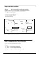
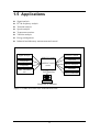
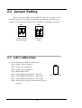
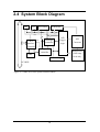
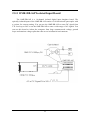
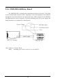
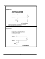
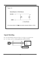
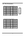
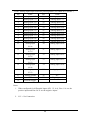
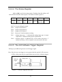
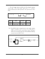
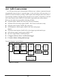
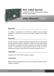
User’s Guide
Shop online at
www.omega.com
e-mail: [email protected]
OME-PCI-1002
PCI Data Acquisition Board
Hardware Manual
OMEGAnet ® Online Service
www.omega.com
Internet e-mail
[email protected]
Servicing North America:
USA:
ISO 9001 Certified
Canada:
One Omega Drive, P.O. Box 4047
Stamford CT 06907-0047
TEL: (203) 359-1660
e-mail: [email protected]
976 Bergar
Laval (Quebec) H7L 5A1, Canada
TEL: (514) 856-6928
e-mail: [email protected]
FAX: (203) 359-7700
FAX: (514) 856-6886
For immediate technical or application assistance:
USA and Canada: Sales Service: 1-800-826-6342 / 1-800-TC-OMEGA®
Customer Service: 1-800-622-2378 / 1-800-622-BEST®
Engineering Service: 1-800-872-9436 / 1-800-USA-WHEN®
TELEX: 996404 EASYLINK: 62968934 CABLE: OMEGA
Mexico:
En Espan˜ol: (001) 203-359-7803
FAX: (001) 203-359-7807
e-mail: [email protected]
[email protected]
Servicing Europe:
Benelux:
Postbus 8034, 1180 LA Amstelveen, The Netherlands
TEL: +31 (0)20 3472121
FAX: +31 (0)20 6434643
Toll Free in Benelux: 0800 0993344
e-mail: [email protected]
Czech Republic:
Frystatska 184, 733 01 Karviná, Czech Republic
TEL: +420 (0)59 6311899
FAX: +420 (0)59 6311114
Toll Free: 0800-1-66342
e-mail: [email protected]
France:
11, rue Jacques Cartier, 78280 Guyancourt, France
TEL: +33 (0)1 61 37 29 00
FAX: +33 (0)1 30 57 54 27
Toll Free in France: 0800 466 342
e-mail: [email protected]
Germany/Austria: Daimlerstrasse 26, D-75392 Deckenpfronn, Germany
TEL: +49 (0)7056 9398-0
Toll Free in Germany: 0800 639 7678
e-mail: [email protected]
United Kingdom:
ISO 9002 Certified
FAX: +49 (0)7056 9398-29
One Omega Drive, River Bend Technology Centre
Northbank, Irlam, Manchester
M44 5BD United Kingdom
TEL: +44 (0)161 777 6611
FAX: +44 (0)161 777 6622
Toll Free in United Kingdom: 0800-488-488
e-mail: [email protected]
It is the policy of OMEGA to comply with all worldwide safety and EMC/EMI regulations that
apply. OMEGA is constantly pursuing certification of its products to the European New Approach
Directives. OMEGA will add the CE mark to every appropriate device upon certification.
The information contained in this document is believed to be correct, but OMEGA Engineering, Inc. accepts
no liability for any errors it contains, and reserves the right to alter specifications without notice.
WARNING: These products are not designed for use in, and should not be used for, patient-connected applications.
Table of Contents
1.
2.
3.
4.
INTRODUCTION................................................................................................................................. 5
1.1
GENERAL DESCRIPTION ............................................................................................................ 5
1.2
THE BLOCK DIAGRAMS................................................................................................................. 6
1.3
FEATURES .................................................................................................................................... 7
1.4
SPECIFICATIONS ........................................................................................................................... 8
1.4.1
Power Consumption ........................................................................................................... 8
1.4.2
Analog Inputs....................................................................................................................... 8
1.4.3
D/I and D/O ............................................................................................................................ 9
1.4.4
A/D Trigger Methods ............................................................................................................ 9
1.4.5
Interrupt Channel ................................................................................................................ 10
1.4.6
Programmable Timer/Counter ........................................................................................ 10
1.5
APPLICATIONS ............................................................................................................................ 11
1.6
PRODUCT CHECK LIST ............................................................................................................... 12
HARDWARE CONFIGURATION ................................................................................................... 13
2.1
BOARD LAYOUT ........................................................................................................................ 13
2.2
JUMPER SETTING ....................................................................................................................... 14
2.3
AD CALIBRATION ...................................................................................................................... 14
2.4
SYSTEM BLOCK .......................................................................................................................... 15
2.5
DAUGHTER BOARDS .................................................................................................................... 16
2.5.1
OME-DB-1825....................................................................................................................... 16
2.5.2
OME-DB-8225..................................................................................................................... 16
2.5.3
OME-DB-37......................................................................................................................... 16
2.5.4
OME- DN-37 ........................................................................................................................ 16
2.5.5
OME-DB-16P Isolated Input Board...................................................................................... 17
2.5.6
OME-DB-16R Relay Board ................................................................................................. 18
2.6
ANALOG INPUT SIGNAL CONNECTION ......................................................................................... 19
2.7
JUMPER SETTING ......................................................................................................................... 23
2.8
THE CONNECTORS ..................................................................................................................... 24
I/O REGISTERS ................................................................................................................................ 26
3.1
HOW TO FIND THE I/O ADDRESS ................................................................................................ 26
3.2
THE I/O ADDRESS MAP ............................................................................................................... 28
3.2.1
Section 1............................................................................................................................... 29
3.2.2
Section 2............................................................................................................................... 30
FUNCTION OPERATION ................................................................................................................ 35
4.1
DIGITAL I/O ............................................................................................................................... 35
3
4.2
THE 8254 TIMER ........................................................................................................................ 36
4.3
THE A/D TRIGGER ..................................................................................................................... 36
4.4
A/D CONVERSION ....................................................................................................................... 38
4.4.1
A/D Conversion Trigger Modes............................................................................................. 40
4.4.2
A/D Transfer Modes............................................................................................................... 40
4.4.3
Software trigger and Polling technique................................................................................. 41
5.
SOFTWARE AND DEMO PROGRAM.......................................................................................... 44
6.
DIAGNOSTIC PROGRAM.............................................................................................................. 45
6.1
POWER-ON PLUG & PLAY TEST ................................................................................................ 45
6.2
DRIVER PLUG & PLAY TEST ...................................................................................................... 45
6.3
D I/O TEST .................................................................................................................................. 46
6.4
A/D TEST ................................................................................................................................... 46
4
1. Introduction
The OME-PCI-1002H/L card provides 12-bit ADC and two 16-bit digital I/O ports.
1.1 General Description
The OME-PCI-1002L and OME-PCI-1002H are high performance multifunction
cards, with A/D and digital I/O for PC and compatible computers in a 5V PCI slot. This
family has the following features: one 12-bit 110K A/D converter, 16 channels D/I, 16
channels D/O, programmable interrupt source and true “Plug and Play” support. The
OME-PCI-1002H/L provides 32 single-ended analog inputs or 16 differential analog
inputs, which are jumper selectable. The OME-PCI-1002L is the low-gain model
equipped with a high speed PGA (programmable gain amp.) with programmable gain
control of 1,2,4,8. The OME-PCI-1002H is the high-gain model equipped with a highgain/high-resolution PGA with programmable gain control of 1,10,100,1000. There are 16
channels of TTL compatible digital output and 16 channels of TTL compatible digital
input. This series provides three programmable trigger methods: software trigger, pacer
trigger and external trigger. The external trigger can be configured as a post-trigger, pretrigger or external pacer trigger. There are also several selectable interrupt sources: A/D
conversion interrupt, pacer interrupt and external interrupt. This multifunction card also
provides an A/D buffer and a data transfer rate of 2.7M words per second in non-burst
mode. This powerful A/D control mechanism offers flexibility for various applications
while minimizing system I/O overhead. The OME-PCI-1002 series is fully “Plug and
Play” compatible and can operate at the full speed of the PCI bus (33MHz). This
important feature makes the OME-PCI-1002 a high performance, cost effective solution
for most data acquisition applications.
5
1.2 Block Diagram
X86 System
PCI BUS
EPROM
PCI Interface System
Status
Control
Local System Controller
Interrupt
Digital Inputs
16 bits DI
16 bits DO
Pacer
Generator
Digital Outputs
4MHz
A/D control logic
A/D
Data
Buffer
12-bit A/D
Converter
Gain
Mux
Figure 1-1. The OME-PCI-1002 series block diagram.
6
Analog Inputs
1.3 Features
•
Bus: 5V PCI (Peripherals Component Interface) bus.
1.
•
•
•
•
•
A/D:
One A/D converter with maximum 110K samples/second.
32 single-ended / 16 differential programmable inputs for OME-PCI-1002L/H.
Three different A/D trigger methods.
Three different external trigger methods.
Programmable gain control, programmable offset control.
2. DIO:
• 16 digital inputs and 16 digital outputs (TTL compatible).
• High-speed data transfer rate: 2.7M word/sec (non-burst mode).
3. Timer:
• One 16-bit machine independent timer for software (Timer 2).
• Two 16-bit pacer timer for A/D converter and interrupt (Timer0, Timer1).
7
1.4 Specifications
1.4.1 Power Consumption
•
•
+5V @ 960mA maximum, OME-PCI-1002L/H
Operating temperature : 0°C to +70°C
1.4.2 Analog Inputs
•
•
•
•
•
•
•
Channels: ( software programmable )
32 single-ended inputs/16 differential inputs, jumper selectable.
Gain control : ( software programmable )
OME-PCI-1002H, Gains - 1, 10, 100, 1000.
OME-PCI-1002L, Gains - 1, 2, 4, 8.
Input signal range :
OME-PCI-1002L: Bipolar
Range: ±10, ±5V, ±2.5V, ±1.25V
OME-PCI-1002H: Bipolar
Range: ±10, ±1V, ±0.1V, ±0.01V
Input current: 250 nA max (125 nA typical) at 25 °C.
Over voltage: continuous single channel to 70Vp-p
Input impedance:
OME-PCI-1002H/L: 1010Ω // 6pF
8
1.4.3 D/I and D/O
•
•
Channels: 16 channels DI, 16 channels DO
DO: Digital output port
Output level: TTL compatible
Output current:
•
Ioh = 0.5mA, Iol = 8mA
DI: Digital input port
Input level: TTL compatible
Input current: 50uA (max)
1.4.4 A/D Trigger Methods
•
Trigger-methods :
1. Software trigger
2. Pacer trigger: 16-bit programmable timer/counter
3. External trigger: Pre-trigger, Post-trigger, external Pacer trigger
Pacer or software trigger
External trigger
CHn
CHn
t
Start
End
Normal trigger mode
Start
End
t
Post-trigger mode
External trigger
External trigger
CHn
CHn
Start
End
t
Start
External pacer trigger mode
Pre-trigger mode
Figure 1-2. Trigger methods of OME-PCI-1002.
9
End
t
1.4.5 Interrupt Channel
•
•
•
Interrupt:
INTA (Automatically assigned by PCI-controller).
Enable/Disable: Via PCI control register and add-on control register.
Interrupt source: (Selected by on-board control register)
1. A/D conversion interrupt
2. Pacer 0 interrupt (Timer 0)
3. Pacer 1 interrupt (Timer 1)
4. External interrupt
1.
End of Conversion
2.
Pacer 0
A/D busy
IRQ
IRQ
3.
Falling edge of Pacer 0
Falling edge of
External trigger
4.
Falling edge of Pacer 1
Pacer 1
External
Trigger
IRQ
IRQ
Figure 1-3. Programmable interrupt source.
1.4.6 Programmable Timer/Counter
•
•
•
Type: 82C54-8 programmable timer/counter.
Timers:
1. Timer 0 for Pacer trigger and interrupt
2. Timer 1 for External trigger and interrupt
3. Timer 2 for software machine independent timer
Input Clock: 4 MHz.
10
1.5 Applications
z
z
z
z
z
z
z
z
Signal analysis.
FFT & frequency analysis.
Transient analysis.
Speech analysis.
Temperature monitor.
Vibration analysis.
Energy management.
Industrial and laboratory measurement and control.
Signal Analysis
Multi-I/O signals
Transition
Temperature
Frequency
Other Laboratory
use
Process Control
OME-PCI-1002
series
Speech Analysis
Vibration
PCI interface
Single-task or multitask
Figure 1-4. OME-PCI-1002 series multifunction cards.
11
Process Monitor
1.6 Product Check List
In addition to this manual, the package includes the following items:
• One OME-PCI-1002 card
• One CD-ROM
Release Notes
The release notes contain the latest information updates. We strongly suggest that you
read them first.
12
2. Hardware Configuration
2.1 Board Layout
CON3
CON2
Figure 2-1. OME-PCI-1002 board layout.
13
VR2
JP1 VR1 VR3
OME-PCI-1002L
CON1
2.2 Jumper Setting
There is only one jumper on the OME-PCI-1002. JP1 is used to select
the analog input type. For single-ended inputs, users should connected pin 1, 3
and pin 2, 4. For differential inputs, Pin 3, 5 and Pin 4, 6 should be connected.
JP1
JP1
1
2
5
6
Single-ended
Inputs (Default)
1
2
5
6
Differential
Inputs
2.3 A/D Calibration
•
A/D Calibration for OME-PCI-1002 card
Step 1: Apply +10V to channel 0.
Step 2: Apply +0V to channel 1.
Step 3: Apply -10V to channel 2.
Step 4: Run DEMO6.EXE.
Step 5: Adjust VR1 until channel 0 = fff or ffe
Step 6: Adjust VR2 until channel 1 = 800 or 801
Step 7: Adjust VR3 until channel 2 = 000 or 001
Step 8: Repeat Step 4 & Step 5 & Step 6 until all read
properly.
14
VR1, VR2, VR3
2.4 System Block Diagram
D/I
D/O
8254 Timer
A/D Buffer
Data
PCI
Interface
Controller
Adr
Interrupt
controller
A/D
Trigger
Logic
Dispatch
controller
NVRA
External Trigger
PCI BUS
Figure 2-2. OME-PCI-1002 System Function Block.
15
A/D
Converter
Multiplexers,
Gain Amp.
Scale Adj.
2.5 Daughter Boards
2.5.1 OME-DB-1825
The OME-DB-1825 is a daughter board designed for 32-channel AD cards such as
the OME-PCI-1002. Refer to the OME-DB-1825 user manual for details.
37pin cable
2.5.2 OME-DB-8225
The OME-DB-8225 provides a on-board CJC (Cold Junction Compensation)
circuit for thermocouple measurement and a terminal block for easy signal connection.
The CJC is connected to A/D channel_0. The OME-PCI-1002 can connect CON3 direct
to the OME-DB-8225 through a 37-pin D-sub connector. Refer to the OME-DB-8225
user manual for details.
2.5.3 OME-DB-37
The OME-DB-37 is a general purpose daughter board for boards with D-sub 37 pin
connectors. It is designed for easy wiring.
2.5.4 OME-DN-37
The OME-DN-37 is a DIN rail mount general purpose daughter board for boards with
D-sub 37 pin connectors. It is designed for easy wiring.
37pin cable
16
2.5.5 OME-DB-16P Isolated Input Board
The OME-DB-16P is a 16-channel isolated digital input daughter board. The
optically isolated inputs of the OME-DB-16P consist of a bi-directional optocoupler with
a resistor for current sensing. You can use the OME-DB-16P to sense DC signal from
TTL levels up to 24V or use the OME-DB-16P to sense a wide range of AC signals. You
can use this board to isolate the computer from large common-mode voltage, ground
loops and transient voltage spike that often occur in industrial environments.
17
2.5.6 OME-DB-16R Relay Board
The OME-DB-16R, 16-channel relay output board consists of 16 form C relays that
can be switched under program control. Applying 5 volts to the appropriate relay channel
through the 20-pin flat connector can energize the relays. Each relay has its own LED that
will light when the relay is energized. To avoid overloading your PC’s power supply, the
board provides screw terminals for external power.
Note: Channel: 16 Form C Relay
Relay: Switching up to 0.5A at 110ACV or 1A at 24 DCV
18
2.6 Analog Input Signal Connection
The OME-PCI-1002 can measure signals in the single-ended or differential mode.
In the differential mode each channel has a unique signal HIGH and signal LOW
connection. In the single-ended mode all channels have a unique signal HIGH connection
but share a common LOW or ground connection. Differential connections are very useful
for low level signals (millivolt), since they better reject electrical noise that can affect the
quality of the measurement. A differential connection is also necessary when a common
ground is unacceptable. The benefit of using a single-ended connection is that twice the
number of channels is available. In general, a single-ended connection is often a good
choice when working with higher level signals (5V or 10V for example), especially if the
signal is coming from an isolated device such as a signal conditioner. Several different
types of wiring diagrams are discussed below.
Figure 2-3A shows a differential connection to a grounded source. If the source is
grounded, making a second connection to the card’s ground could cause a ground loop
resulting in erroneous data. It is important to note that the maximum common mode
voltage between the input source and AGND is 70Vp-p. If the card is connected to a
source with a common mode voltage greater than 70Vp-p, the input multiplexer will
be permanently damaged! When measuring common mode voltage, it is best to use an
oscilloscope rather than a multi-meter.
Figure 2-3B shows a differential connection to a floating source. In such cases a
connection should be made between the low channel input and analog ground.
Figure 2-4 shows connection of multiple sources in single-ended mode. This
connection assumes creating one common ground will not cause a problem. This is
normally the case when connecting to devices that are isolated or floating.
Figure 2-5 demonstrates how to connect bridge transducers. Bridge transducers
include strain gauges, load cells and certain type of pressure transducers. The diagram
assumes that there is a single external power supply providing power to the bridge. Each
bridge is connected to a differential channel. No connection is made between channel
low and analog ground. A connection should be made between analog ground and the
negative of the power supply. An isolated power supply is strongly suggested.
Figure 2-6 demonstrates how to connect a 4-20mA current loop. Since the card
reads voltages, the current is converted to voltage by passing it through a shunt resistor.
By Ohms law (V=IR), when using a 250Ω resistor, 4 mA will be converted to 1V and
20mA to 5V. If the source is linear, the output voltage range will also be linear.
19
Figure 2-3A
If the source is grounded, a second ground connection
on the card could result in a ground loop.
Figure 2-3B
20
Figure 2-4
Figure 2-5
21
Figure 2-6
R is a shunt resistor. A 250Ω shunt resistor converts 4-20mA to 1-5Vdc.
Signal Shielding
z
z
The signal shielding connections in Figure 2-3 to Figure 2-6 are all the same
Use a single connection to frame ground (not A.GND or D.GND)
OME-PCI-1002
A.GND
D.GND
Vin
Frame Ground
22
2.7 Jumper Settings
There is only one jumper on the OME-PCI-1002. JP1 is used to select
the analog input type. For single-ended inputs, users should connect Pin-1, 3
and Pin-2, 4. For differential inputs, Pin-3, 5 and Pin-4, 6 should be
connected.
JP1
JP1
1
2
5
6
1
2
5
6
Single-ended
Differential
Inputs (Default)
Inputs
23
2.8 The Connectors
CON1: Digital output connector pin assignment.
Pin
Name
Pin
Name
1
Digital output 0
2
Digital output 1
3
Digital output 2
4
Digital output 3
5
Digital output 4
6
Digital output 5
17
Digital output 6
8
Digital output 7
9
Digital output 8
10
Digital output 9
11
Digital output 10
12
Digital output 11
13
Digital output 12
14
Digital output 13
15
Digital output 14
16
Digital output 15
17
PCB ground
18
PCB ground
19
PCB +5V
20
PCB +12V
CON2: Digital input connector pin assignment.
Pin
Name
Pin
Name
1
Digital input 0
2
Digital input 1
3
Digital input 2
4
Digital input 3
5
Digital input 4
6
Digital input 5
17
Digital input 6
8
Digital input 7
9
Digital input 8
10
Digital input 9
11
Digital input 10
12
Digital input 11
13
Digital input 12
14
Digital input 13
15
Digital input 14
16
Digital input 15
17
PCB ground
18
PCB ground
19
PCB +5V
20
PCB +12V
24
1
3
5
7
9
11
13
15
17
19
2
4
6
8
10
12
14
16
18
20
CON3: Analog input/output connector pin assignment. (For OME-PCI-1002H/L)
Pin
Name
Pin
Name
1
Analog input 0/0+
20
Analog input 16/0-
2
Analog input 1/1+
21
Analog input 17/1-
3
Analog input 2/2+
22
Analog input 18/2-
4
Analog input 3/3+
23
Analog input 19/3-
5
Analog input 4/4+
24
Analog input 20/4-
6
Analog input 5/5+
25
Analog input 21/5-
7
Analog input 6/6+
26
Analog input 22/6-
8
Analog input 7/7+
27
Analog input 23/7-
9
Analog input 8/8+
28
Analog input 24/8-
10
Analog input 9/9+
29
Analog input 25/9-
11
Analog input
10/10+
30
Analog input 26/10-
12
Analog input
11/11+
31
Analog input 27/11-
13
Analog input
12/12+
32
Analog input 28/12-
14
Analog input
13/13+
33
Analog input 29/13-
15
Analog input
14/14+
34
Analog input 30/14-
16
Analog input
15/15+
35
Analog input 31/15-
17
Analog ground
36
N.C.
18
N.C.
37
Digital ground
19
External trigger
Notes:
1. When configured for differential inputs (JP1 3-5, 4-6), Pins 1-16 are the
positive inputs and Pins 20-35 are the negative inputs.
2.
N.C. = No Connection
25
3. I/O Registers
3.1 How to Find the I/O Address
The Plug & Play BIOS will assign a valid I/O address to all OME-PCI-1002 cards in
the system during the computer’s power-on stage. The ID numbers of OME-PCI-1002
are shown below:
• Vendor ID
• Device ID
= 1234
= 1002
Associated Driver Functions:
1. P1002_DriverInit(&wBoard)
This function detects the number of OME-PCI-1002 cards in the system.
• wBoard=1 Æ only one OME-PCI-1002 in this PC system.
• wBoard=2 Æ there are two OME-PCI-1002 in this PC system.
2. P1002_GetConfigAddressSpace(wBoardNo, *wBase, *wIrq, *wPLX)
Use this function to determine the resources for all cards installed in the system.
This is used when writing directly to the card’s I/O addresses.
• wBoardNo=0 to N Æ totally N+1 cards of OME-PCI-1002
• wBase Æ base address of the board control word
• wIrq
Æ allocated IRQ channel number of this board
• wPLX Æ base address of PCI-interface-IC
26
The sample program code is shown below:
/* Step1: Detect all OME-PCI-1002 card first */
wRetVal=P1002_DriverInit(&wBoards);
printf("There are %d OME-PCI-1002 Cards in this PC\n",wBoards);
/* Step2: save resource of all OME-PCI-1002 cards installed in this PC */
for (i=0; i<wBoards; i++)
{
P1002_GetConfigAddressSpace(i,&wBase,&wIrq,&wPLX);
printf("\nCard_%d: wBase=%x, wIrq=%x, wPLX=%x", i,wBase,wIrq,wPLX);
wConfigSpace[i][0]=wBaseAddress; /* save all resource of this card */
wConfigSpace[i][1]=wIrq;
/* save all resource of this card */
wConfigSpace[i][2]=wPLX;
/* save all resource of this card */
}
/* Step3: control the OME-PCI-1002 directly */
wBase=wConfigSpace[0][0];
/* get base address the card_0
outpw(wBase+0x20,wDoValue);
/* control the D/O states of card_0
wDiValue=inpw(wBase+0x20);
/* read the D/I states of card_0
wBase=wConfigSpace[1][0];
outpw(wBase+0x20,wDoValue);
wDiValue=inpw(wBase+0x20);
wPLX=wConfigSpace[2][2];
_outpd(wPLX+0x4c,0x41);
…
…
…
_outpd(wPLX+0x4c,0);
/* get base address of card_1
/* control the D/O states of card_1
/* read the D/I states of card_1
*/
*/
*/
*/
*/
*/
/* get PCI-interface base address of card-2 */
/* channel_1, interrupt active_Low
*/
/* disable all interrupts
27
*/
3.2 The I/O Address Map
The OME-PCI-1002 registers are given below. The address of each register
is determined by adding the offset to the base address of the corresponding
section.
Section
Offset
Name
Access
Length
1
4ch
PCI interrupt control
register
R/W
8/16/32 bits
00h
8254 timer1
R/W
8/16/32 bits
04h
8254 timer2
R/W
8/16/32 bits
08h
8254 timer3
R/W
8/16/32 bits
0Ch
8254 control register
W
8/16/32 bits
10h
Analog input channel
control register
W
10h
Status register
R
8/16/32 bits
14h
Analog input gain
control register
W
8/16/32 bits
18h
General control
register
W
1Ch
A/D software trigger
W
8/16/32 bits
1Ch
Clear Interrupt
R
8/16/32 bits
20h
Digital output register
W
16/32 bits
20h
Digital input register
R
16/32 bits
30h
A/D data register
R
16/32 bits
2
28
8/16/32 bits
8/16/32 bits
3.2.1 Section 1
Although there are 128 I/O ports used by the on-board PCI interface
controller, only one register is used for most applications. The user should
not modify the other registers! The PCI interrupt control register (4Ch)
controls the interrupts generated by the system. The register is set to “disable
interrupt” after power-on or hardware reset signal, thus no interrupts will be
generated before this register is activated even if the user enables the add-on
interrupt! In order to enable the PCI-interrupt, write 43h to this register. Write
03h to this register if you want to disable the PCI interrupts.
Following is the format of the PCI interrupt control register:
Bit 31-Bit 7
Bit6
Not used
Interrupt Enable
Bit5-Bit3
Bit2
Bit1-Bit0
Not used Interrupt Flag Interrupt Select
Bit 6: Write an ‘1’ to enable the PCI-interrupt and a ‘0’ to disable PCI interrupt.
Bit 2: This bit is read-only. A ‘1’ indicates that the Add-on has
generated an interrupt, ‘0’ means that Add-on did not generate an interrupt.
Bit1-0: Always write 1 to these two bits.
Note:
1. Since the OME-PCI-1002 supports “Plug and Play”, the interrupt
number will automatically be assigned by your system. The user can
determine the interrupt number by using standard PCI utilities or by
using the OME-PCI-1002 software driver.
2. If your system supports “Shared IRQ”, several peripherals may
share the same IRQ at the same time. You must use Bit-2 to find out
if an IRQ was generated from the OME-PCI-1002 or a different
device!
3. For more information about the PCI interrupt control, please refer to
the user reference manual of the PLX-9050.
29
3.2.2
Section 2
This group of registers is used by the add-on control logic. 64 bytes of
I/O locations are used. Their detailed descriptions are shown below
3.2.2.1 The 8254 Registers
The 8254, programmable timer/counter, is used to generate periodic
interrupts, A/D trigger and the machine independent timer. Addresses 00h,
04h, 08h and 0Ch are used to program the 8254.
Timer 0 is used as Pacer 0 and timer 1 is used as Pacer 1. Timer 2 is used
as the machine independent timer (P1002_Dealy() function). Refer to Intel’s
“Microsystem Components Handbook” for detailed programming information.
3.2.2.2 The DI / DO Register
Address 20h is used for DI / DO ports. Write to this port to send data to
the DO register. Read from this port to input DI data.
3.2.2.3 The A/D Buffer
Address 30h is used for the A/D buffer. This is a read-only address.
Reading from this port will return the data from A/D buffer. The format of A/D
buffer is:
Bit15-12
Bit11-0
Analog input
channel
A/D data
Bit15-12: The channel number of the analog input. Only lower 4 bits of
channel number are shown in this register.
Bit11-0: The A/D data.
30
3.2.2.4 The Status Register
Address 10h is used is the status register. Reading from this address will
return the data from the status register. The format of status register is:
Bit7-6
Bit5
Gain
Control
8245
Timer 1
Bit4
Bit3
Bit2
Bit1
Bit0
8245
8245
Analog A/D Busy
Reserved
Timer 0 Timer 2
input type
Bit 7-6: Current A/D gain control.
Bit 5 : Output of 8254 timer 1.
Bit 4 : Output of 8254 timer 0.
Bit 3 : Output of 8254 timer 2.
Bit 2 : Reserved. Used for hardware testing.
Bit 1 : Analog input type, ‘1’ indicated that analog input type is singleended and ‘0’ indicated analog input is differential.
Bit 0 : A/D busy signal. ‘0’ indicates busy, A/D is under conversion. ‘1’
indicates not busy, A/D is complete conversion and is idle now.
3.2.2.5 The A/D Software Trigger Register
Writing to port 1Ch will generate an A/D trigger signal.
Note: Since the user can trigger at a rate greater than the speed of A/D converter
(125K), a delay time may be required between successive software triggers
Software
trigger
A/D
Busy
Delay time
8 µs
Conversion Time
Figure 3-1. Software triggered delay time.
31
3.2.2.6 Clear Interrupt
Reading from 1Ch will clear the add-on interrupt.
3.2.2.7 The Analog Input Selection Register
…
Analog inputs
The analog input channel selection register uses address 10h and
address 14h is used by the analog gain control selection register. Write 0-31 to
port 10h to select the channel number (for differential input, write 0-15).
Write 0-3 to port 14h to select the gain control.
Analog
Mux.
ADC
AMP
Select
Gain control
…
Channel select
Figure 3-2. Analog input control.
Note:
1.
2.
For single ended inputs, channels 0-31 are available. For
differential inputs, channels 0-15 are available. If you enter a
channel number greater than the number available, those channels
will be ignored. Thus, for single-ended inputs, only the last 5 bits
are taken as the channel number. And for differential inputs, only
the last 4 bits are taken as the channel number.
Only the last two digits are used as the gain control code. The gain
control codes and corresponding gains are shown below :
For OME-PCI-1002L:
Gain code
[0 0]
[0 1]
[1 0]
[1 1]
Gain
1
2
4
8
32
For OME-PCI-1002H:
3.
[Bit1,Bit0]
[0 0]
[0 1]
[1 0]
[1 1]
Gain
1
10
100
1000
These registers are set to 0 after power-on or a hardware reset signal.
3.2.2.8 The General Control Register
The general control register (18h) is used to control the add-on interrupt
source and the A/D trigger method. The format of this register is:
Bit4-2
Bit 1-0
Interrupt source
selection register
A/D trigger method
selection register
3.2.2.8.1 Interrupt Source Selection
There are four interrupt sources selectable for the OME-PCI-1002 (see
section 1.4.4).
[Bit4,Bit3,Bit2]
Description
[ 0, 0, 0 ]
No interrupt source, disable all interrupts.
[ 0, 0, 1 ]
Interrupt after A/D conversion completes.
[ 0, 1, 0 ]
Interrupt after 8254 timer 0 falling.
[ 0, 1, 1 ]
Interrupt after external trigger falling.
[ 1, 0, 0 ]
Interrupt after 8254 timer 1 falling.
Others
No interrupt source, disable all interrupts.
Note: Bit 3-3 of general control register is set to 0 after a hardware reset.
33
3.2.2.8.2 Trigger Method Selection
There are several trigger methods that can be selected by the user (see
section 1.4.5):
[Bit1,Bit0 ]
Descriptions
[ 0, 0 ]
General trigger mode.
8254 timer 0 trigger (internal pacer trigger ) or software
trigger.
[ 0, 1 ]
External clock trigger mode.
[ 1, 0 ]
Pre-trigger mode.
[ 1, 1 ]
Post-trigger mode.
Note:
1. In the general trigger mode, both the 8254 timer 0 and the software
trigger are used as the A/D trigger signals. The timer 0 and the software
trigger should not be used at the same time! This means the user
2.
3.
4.
5.
should not generate a software trigger while the 8254 timer 0 is
activated!
In the external clock trigger mode, an external input is taken as the A/D
trigger signal. A single falling edge of the external trigger will generate
a single A/D trigger.
The pre-trigger mode employs the 8254 timer 1. The user should first
configure timer 1, then set the trigger mode to pre-trigger. Once the
pre-trigger mode has been activated, it will automatically turn on timer
1 and start the A/D trigger. This will continue until a falling edge from
an external trigger signal is received. Any change to the trigger mode
selection will turn off the pre-trigger mode.
The post-trigger mode employs the 8254 timer 1. The user should first
configure timer 1, then set the trigger mode to post-trigger. Once the
post-trigger mode has been activated, it will automatically turn off the
timer 1 until it receives a falling edge from an external signal. Any
change to the trigger mode selection will turn off the post-trigger mode.
The A/D trigger selection is set to 0 after power-on or hardware reset.
34
4. Function Operation
4.1 Digital I/O
The OME-PCI-1002 series provides 16 digital input channels and 16 digital
output channels. All signals are TTL compatible. The connector and block diagrams
are given below:
CN2
BaseAddr+20h
read signal.
DI port
Local Data Bus
D0 ... D15
BaseAddr+20h
write signal
DO port
CN1
Figure 4.1. DIO function diagram.
35
4.2 The 8254 Timer
The OME-PCI-1002 series provide 3 independent 16-bit
timer/counters. Each timer has a different function. Timer 0 is used as
Pacer 0. Timer 1 is used as Pacer 1. Timer 2 is used as the machine
independent timer. The block diagram is given as follows:
VCC
4 M Hz
EN
CLK
Timer 0
Pacer 0
OUT1
Local Data Bus
CLK
D0…D7
Timer 1
User
EN
Pacer 1
OUT2
CLK
Status
Timer
EN
8254
OUT3
Figure 4-2. 8254 Block Diagram.
4.3 The A/D trigger
The block diagram of the A/D trigger is shown below:
8254
Timer 0
Software Trigger
0
1
External
Trigger.
D
PR
External Trigger
Q
RS
Mux
EN
CLK
8254
Timer 1
4M-Hz
Figure 4-3. A/D Trigger Controller.
36
Select
Trigger Select
To A/D
The A/D trigger logic can initiate an A/D conversion upon an
external trigger. Valid external trigger signals must be TTL compatible
and meet minimum pulse width requirements. The requirements are shown
below:
External trigger
tdu
tre
Symbol
Name
Minimum
Maximum
Tdu
Duration time
40ns
∞
Tre
Recover time
100ns
∞
Note: The OME-PCI-1002 is designed only for time sensitive triggers
(trigger is dependent only on the time of the falling edge of
signal). For a level sensitive external trigger (trigger is dependent
on the level of the input signal), the user can build the following
external circuit the OME-PCI-1002:
Comparator
Input Signal
OME-PCI1002 D/O
External
Trigger
DAC
TTL buffer
37
4.4 A/D Conversion
An A/D conversion can be initiated three different ways: software command, internal
programmable interval timer or external trigger. At the end of the A/D conversion, it is
possible to transfer the data by polling a status register and reading the data when ready or
by generating a hardware interrupt and an interrupt service routine. All modes are selected
by a control register on the OME-PCI-1002 and are supported by the utility software.
Below are key points for successfully collecting A/D data:
z A/D data register, BASE+30h, stores the A/D conversion data.
z A/D data conversion ready register, BASE +10h. Check if A/D data is ready.
z A/D gain control register, BASE+14h, select gain.
z A/D multiplexer control register, BASE+10h, select analog input
channel.
z A/D mode control register, BASE+0Ch, select trigger type and transfer type.
z
z
A/D software trigger control register, BASE+1Ch.
JP1 select single-ended or differential input.
z
z
3 Triggers: Software, Pacer, and External trigger.
2 Transfer Modes: Polling and Interrupt.
The block diagram is given follows:
CN3
16/8 to 1
Multiplexer
Gain
Control
BASE+10h
BASE+14h
12 bits
A/D
Trigger
Logic
BASE+1Ch
Software Trigger
OME-PCI-1002H/L
38
Buffer
BASE+30h
Memory
CPU
Before performing A/D conversions, the JP1 jumper should be set for single-ended or
differential.
The software driver supports both polling and interrupt driven A/D, however, polling
is the simplest way to perform an A/D conversion.
The settling time of multiplexer depends on the impedance of the signal source.
Because the driver does not incorporate the settling time, the user needs to program a
delay when switching from one channel to another or when changing gains.
Suggested Settling Times
One settling time is suggested for all ranges of the OME-PCI-1002L. The settling time
for the OME-PCI-1002H is based on the analog input range. The table below shows the
suggested settling times for each range.
OME-PCI-1002L Settling Time: 33 µseconds for all ranges
OME-PCI-1002H Settling Time
Input Range
Settling Time
± 10V
23 µS
± 5V
28 µS
± 0.1V
140 µS
± 0.01V
1300 µS
The software driver provides a machine independent timer, P1002_Delay(), for
settling time delay. If the user calls P1002_Delay(), counter 0 will be reserved and can
not be used as a user programmable timer/counter.
The A/D converter requires a trigger signal to start an A/D conversion cycle. The
OME-PCI-1002 supports three trigger modes, software, pacer and external trigger.
39
4.4.1 A/D Conversion Trigger Modes
The OME-PCI-1002 supports three trigger modes.
1 : Software Trigger :
Write any value to A/D software trigger control register, BASE+1Ch, will initiate a
A/D conversion cycle. This mode is very simple but very difficult to control
sampling rate.
2 : Pacer Trigger Mode :
The block diagram of pacer timer is shown in section 3.2. The sample rate of pacer
is very precise.
3 : External Trigger Mode :
When a rising edge of external trigger signal is applied, an A/D conversion will be
performed. The external trigger source comes from Pin-17 of CON3.
4.4.2A/D Transfer Modes
OME-PCI-1002 supports two transfer modes.
1 : polling transfer :
This mode can be used with all trigger modes. You must disable timer 0 before
polling. The A/D data can be read from the register at BASE+30h. Before reading
the data first check the A/D ready bit at register BASE +10h READY_BIT=0.
2 : interrupt transfer:
This mode can be used with the pacer trigger or an external trigger. A hardware
interrupt signal is sent to the PC when an A/D conversion is completed.
For interrupt transfer, the use of the driver software is strongly recommended.
40
Software Trigger and Polling Techniques
The steps below should be followed for software triggering and polling:
1. Send 00h to A/D mode control register (software trigger + polling transfer)
2. Send channel number to multiplexer control register.
3. Send the gain control code value to gain control register.
4. Send any value to software trigger control register to generate a software trigger
signal.
5. Scan the READY bit of the A/D high byte data until READY=0
6. Read the 12 bits A/D data.
7. Convert the 12 bits binary data to the floating point value.
For example:
/* ------------------------------------------------------------- */
/* DEMO 3: AdPolling
*/
/* Compiler: Borland C++ 3.1, Mode Large
*/
/* Output Code: HEX code
*/
/* -------------------------------------------------------------- */
#include "P1002.H"
WORD wBaseAddr,wIrq;
//------------------------------------------------------WORD P1002_Delay(WORD wDownCount)
{
WORD h,l;
int count;
wDownCount &= 0x7fff;
if (wDownCount<1) wDownCount=1;
/* Clock in=4M --> count 4000 = 1 ms, count 1 = 0.25 us */
l=wDownCount&0xff;
wDownCount=wDownCount / 256;
h=wDownCount&0xff;
outp(wBaseAddr+3*4,0xB0);
/* mode_0, counter_2 */
outp(wBaseAddr+2*4,l);
/* counter_2 low byte first */
outp(wBaseAddr+2*4,h);
/* counter_2 high byte ,0x07D0=2000 */
outp(wBaseAddr+3*4,0x80);
/* latch counter_2 */
41
l=inp(wBaseAddr+2*4);
/* delay starting two clks */
h=inp(wBaseAddr+2*4);
for (count=32767;count>0;count--){
outp(wBaseAddr+12,0x80); /* latch counter_2 */
l=inp(wBaseAddr+8);
h=inp(wBaseAddr+8);
if (h>=0x80) return NoError;
}
return TimeOut;
}
//-------------------------------------------------------void AdPolling(UCHAR channel, UCHAR gain, WORD delay)
{
outp(wBaseAddr+0x18,0);
// Select Mode 0
outp(wBaseAddr+0x10,channel);
outp(wBaseAddr+0x14,gain);
P1002_Delay(delay);
outp(wBaseAddr+0x1c,01);
// A/D software tirgger
}
void SetupTimer(WORD wChannel, WORD wCoef)
{
WORD cmd;
wChannel=wChannel&0x03;
cmd=0x34+(wChannel<<6);
outpw(wBaseAddr+3*4, cmd);
outp(wBaseAddr+wChannel*4, (UCHAR)(wCoef&0xff));
outp(wBaseAddr+wChannel*4, (UCHAR)(wCoef>>8));
}
//=========================================================
void main()
{
int i,j;
WORD wBoards,wRetVal,wPLX;
WORD Drdy,wAdData=0;
42
char c;
clrscr();
P1002_DriverInit(&wBoards);
printf("\n(1) Threr are %d OME-PCI-1002 Cards in this PC",wBoards);
if ( wBoards==0 )
{
putch(0x07); putch(0x07); putch(0x07);
printf("(1) There are no OME-PCI-1002 card in this PC !!!\n"); exit(0);
}
printf("\n(2) Show the Configuration Space of all OME-PCI-1002:");
for(i=0; i<wBoards; i++)
{
P1002_GetConfigAddressSpace(i,&wBaseAddr,&wIrq,&wPLX);
printf("\n
Card_%d: wBaseAddr=%x, wIrq=%x, wPLX=%x",i,wBaseAddr,wIrq,wPLX);
}
P1002_GetConfigAddressSpace(0,&wBaseAddr,&wIrq,&wPLX); /* select card_0 */
printf("\n(3) *** Card_0, wBaseAddr=%x ***\n",wBaseAddr);
SetupTimer(0,1);
// AdPolling have to disable timer 0
AdPolling(0,0,23);
// channel=0, gain=+/-10, delay=23us
for(i=0;i<10;i++)
{
outp(wBaseAddr+0x1c,01);
// A/D software tirgger
while(1)
{
if( ((inpw(wBaseAddr+0x10))&0x01)==1) // check A/D busy?
break;
}
wAdData=((inpw(wBaseAddr+0x30))&0x0fff);
printf("\nRang:+/-10V, Counter %d ,ADC channel 0 value: 0x%xH",i,wAdData);
}
P1002_DriverClose();
}
43
5. Software and Demo Program
1. Demo programs for DOS
• …\1002\BC\LARGE\DEMO>
• …\1002\BC\LARGE\LIB>
← demo program
←library and driver
•
•
•
•
•
•
DEMO1: Digital output.
DEMO2: Digital output and Digital input test by itself.
DEMO3: A/D Polling for channel 0.
DEMO4: A/D Polling for channel 0,1,2,3 and defferent gain 1,2,4,8.
DEMO5: A/D Pacer trigger.
DEMO6: A/D Calibration.
•
DEMO7: Find card number.
2. Demo program for Windows95/98/NT
• Refer to CD-ROM.
44
6. Diagnostic Program
6.1 Power-ON Plug & Play Test
Below are the steps for the power-on Plug & Play test:
Step 1: Power-off the PC
Step 2: Install OME-PCI-1002 without any extra external connections
Step 3: Power-on the PC and watch the PC screen very carefully
Step 4: The PC will perform its self-test first
Step 5: The PC will detect the non-PCI physical devices installed in the system
Step 6: The PC will display the information for these devices
Step 7: The PC will detect the PCI Plug & Play devices installed in the system
All PCI-device information will be shown Æ pay careful attention
Æ There will be a PCI device with vendor_ID=1234, device_ID=1002 (OME-PCI1002)
If the Plug & Play ROM-BIOS successfully detects the OME-PCI-1002 card during
the power-on state, the DOS and Windows software driver will also be able to detect the
card. If the Plug & Play ROM-BIOS can not find the OME-PCI-1002, the software driver
will not function. Therefore the user must make sure that the power-on detection is
correct.
6.2 Driver Plug & Play Test
Step 1: Power-off the PC.
Step 2: Install OME-PCI-1002 without any extra external connector.
Step 3: Power-on PC and run DEMO7.EXE.
Step 4: The I/O base address of all OME-PCI-1002 cards installed in the system will be
displayed.
Step 5: Verify that the total number of boards is correct
Step 6: If more than one card, install a 20-pin flat cable on one of the OME-PCI-1002
45
cards.
Step 7: If a card’s D/O=D/I Æ this is the physical card number, remember this number.
Step 8: Repeat the previous two steps to find the physical card number of all boards.
6.3 D I/O Test
Step 1: Power-off the PC.
Step 2: Install one OME-PCI-1002 card with a 20-pin flat cable between CON1 & CON2.
Step 3: Power-on the PC then run DEMO2.EXE.
Step 4: The DO and DI are displayed as TEST OK or TEST ERROR.
6.4 A/D Test
• A/D Test for OME-PCI-1002 card
Step 1: Power-off the PC.
Step 2: Install one OME-PCI-1002 card.
Step 3: Power-on PC, run DEMO6.EXE
Step 4: Apply +10V to channel 0.
Step 5: Apply +0V to channel 1.
Step 6: Apply -10V to channel 2.
Step 7: Run DEMO6.EXE.
Step 8: Check channel 0 = fff or ffe?
Step 9: Check channel 1 = 800 or 801?
Step 10: Check channel 2 = 000 or 001?
46
WARRANTY/DISCLAIMER
OMEGA ENGINEERING, INC. warrants this unit to be free of defects in materials and workmanship for a
period of 13 months from date of purchase. OMEGA’s WARRANTY adds an additional one (1) month
grace period to the normal one (1) year product warranty to cover handling and shipping time. This
ensures that OMEGA’s customers receive maximum coverage on each product.
If the unit malfunctions, it must be returned to the factory for evaluation. OMEGA’s Customer Service
Department will issue an Authorized Return (AR) number immediately upon phone or written request.
Upon examination by OMEGA, if the unit is found to be defective, it will be repaired or replaced at no
charge. OMEGA’s WARRANTY does not apply to defects resulting from any action of the purchaser, including but not limited to mishandling, improper interfacing, operation outside of design limits,
improper repair, or unauthorized modification. This WARRANTY is VOID if the unit shows evidence of
having been tampered with or shows evidence of having been damaged as a result of excessive corrosion;
or current, heat, moisture or vibration; improper specification; misapplication; misuse or other operating
conditions outside of OMEGA’s control. Components which wear are not warranted, including but not
limited to contact points, fuses, and triacs.
OMEGA is pleased to offer suggestions on the use of its various products. However,
OMEGA neither assumes responsibility for any omissions or errors nor assumes liability for any
damages that result from the use of its products in accordance with information provided by
OMEGA, either verbal or written. OMEGA warrants only that the parts manufactured by it will be
as specified and free of defects. OMEGA MAKES NO OTHER WARRANTIES OR
REPRESENTATIONS OF ANY KIND WHATSOEVER, EXPRESS OR IMPLIED, EXCEPT THAT OF TITLE,
AND ALL IMPLIED WARRANTIES INCLUDING ANY WARRANTY OF MERCHANTABILITY AND
FITNESS FOR A PARTICULAR PURPOSE ARE HEREBY DISCLAIMED. LIMITATION OF
LIABILITY: The remedies of purchaser set forth herein are exclusive, and the total liability of
OMEGA with respect to this order, whether based on contract, warranty, negligence,
indemnification, strict liability or otherwise, shall not exceed the purchase price of the
component upon which liability is based. In no event shall OMEGA be liable for
consequential, incidental or special damages.
CONDITIONS: Equipment sold by OMEGA is not intended to be used, nor shall it be used: (1) as a “Basic
Component” under 10 CFR 21 (NRC), used in or with any nuclear installation or activity; or (2) in medical
applications or used on humans. Should any Product(s) be used in or with any nuclear installation or
activity, medical application, used on humans, or misused in any way, OMEGA assumes no responsibility
as set forth in our basic WARRANTY/ DISCLAIMER language, and, additionally, purchaser will indemnify
OMEGA and hold OMEGA harmless from any liability or damage whatsoever arising out of the use of the
Product(s) in such a manner.
RETURN REQUESTS/INQUIRIES
Direct all warranty and repair requests/inquiries to the OMEGA Customer Service Department. BEFORE
RETURNING ANY PRODUCT(S) TO OMEGA, PURCHASER MUST OBTAIN AN AUTHORIZED RETURN
(AR) NUMBER FROM OMEGA’S CUSTOMER SERVICE DEPARTMENT (IN ORDER TO AVOID
PROCESSING DELAYS). The assigned AR number should then be marked on the outside of the return
package and on any correspondence.
The purchaser is responsible for shipping charges, freight, insurance and proper packaging to prevent
breakage in transit.
FOR WARRANTY RETURNS, please have the
following information available BEFORE
contacting OMEGA:
1. Purchase Order number under which the product
was PURCHASED,
2. Model and serial number of the product under
warranty, and
3. Repair instructions and/or specific problems
relative to the product.
FOR NON-WARRANTY REPAIRS, consult OMEGA
for current repair charges. Have the following
information available BEFORE contacting OMEGA:
1. Purchase Order number to cover the COST
of the repair,
2. Model and serial number of the product, and
3. Repair instructions and/or specific problems
relative to the product.
OMEGA’s policy is to make running changes, not model changes, whenever an improvement is possible. This affords
our customers the latest in technology and engineering.
OMEGA is a registered trademark of OMEGA ENGINEERING, INC.
© Copyright 2002 OMEGA ENGINEERING, INC. All rights reserved. This document may not be copied, photocopied,
reproduced, translated, or reduced to any electronic medium or machine-readable form, in whole or in part, without the
prior written consent of OMEGA ENGINEERING, INC.
Where Do I Find Everything I Need for
Process Measurement and Control?
OMEGA…Of Course!
Shop online at www.omega.com
TEMPERATURE
Thermocouple, RTD & Thermistor Probes, Connectors, Panels & Assemblies
Wire: Thermocouple, RTD & Thermistor
Calibrators & Ice Point References
Recorders, Controllers & Process Monitors
Infrared Pyrometers
PRESSURE, STRAIN AND FORCE
Transducers & Strain Gages
Load Cells & Pressure Gages
Displacement Transducers
Instrumentation & Accessories
FLOW/LEVEL
Rotameters, Gas Mass Flowmeters & Flow Computers
Air Velocity Indicators
Turbine/Paddlewheel Systems
Totalizers & Batch Controllers
pH/CONDUCTIVITY
pH Electrodes, Testers & Accessories
Benchtop/Laboratory Meters
Controllers, Calibrators, Simulators & Pumps
Industrial pH & Conductivity Equipment
DATA ACQUISITION
Data Acquisition & Engineering Software
Communications-Based Acquisition Systems
Plug-in Cards for Apple, IBM & Compatibles
Datalogging Systems
Recorders, Printers & Plotters
HEATERS
Heating Cable
Cartridge & Strip Heaters
Immersion & Band Heaters
Flexible Heaters
Laboratory Heaters
ENVIRONMENTAL
MONITORING AND CONTROL
Metering & Control Instrumentation
Refractometers
Pumps & Tubing
Air, Soil & Water Monitors
Industrial Water & Wastewater Treatment
pH, Conductivity & Dissolved Oxygen Instruments
M3927/0203