1
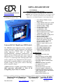
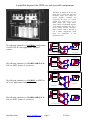
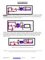
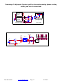
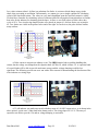
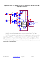
SHPSA-200A400/05F
Operation Manual
Super high-power SPDT (SPCO/SPTT) Switching Apparatus
V
6
V
4
2
0
20
-2
16
-4
12
-6
8
-8
4
-10
0
-4
-10
0
10
20
ch A: Frequency(Hz)
30
40
50
60
70
80
Not enough data
20May2011 15:38
200V applied onto a 1 Ohm load
VS Holding LLC. – http://www.vsholding.com
Manufactured by
Electronic Design & Research, Inc.
7331 Intermodal Drive, Louisville, KY 40258
Data Sheet 9001
www.vsholding.com
Page 1
11/8/2011
-8
90 ms
Electronic Design & Research is a pioneer in developing and manufactures high-speed, high-power
relays/switches. Starting since 1998, we have produced vast varieties of Solid-State Modules and Devices.
Our products have being used in thousand Defense related and industrial applications.
Piezo Drivers
Video Switches
½ Bridge drivers
Q-type high-pass filters
Precision F-to-V Converters
Soft-Landing Solenoid Drivers
50Hz/60Hz Comb Notch filters
Super-high Po wer, fast Switches
H-bridge or Full-bridge Drivers
High-power, high-speed Switches
Universal Analog Building Module
Signal Switching Separating Network
Sockets for relays, switches and drivers
Charge-Pump Wide-Band FM detectors
Low-Noise, High-Voltage DC/DC converters
DC-3phase AC resonance mode driver for EV
DC-12phase AC resonance mode driver for EV
Perpetual Pulse-width Discriminator, US Patent
½ and H Fuzzy Logic sockets for various relays
Fuzzy-Logic SPDT Relays, Switches and ½ Drivers
Fully protected, Solid-State DPST Brake, US Patent
Single Pole, Single Trout Relays and Switches, (SPST)
Power-distributing module for Motorcycles, US Patent
Single Pole, Double Trout Relays and Switches, (SPDT)
Double Pole, Single Trout Relays and Switches, (DPST)
1-Form B, SPST-NC (normally closed) Solid State Relays
Charge-and-Add, Up/Down DC/DC Converters, US patent
1-Form B and 1-Form A, DPST-NC/NO Solid State Relays
µ-Power Controller for Magnetic Latching Valves, US Patent
High Voltage, Nana-Seconds Rise/Fall time, Push-Pull Drivers
Super-low noise preamplifiers for a low and high impedance sources
µ-control, High-Power SPST-NC, normally closed relays, US Patent
We are working hard bringing new devices to the market to meet your technological needs. Above is
a list of family of devices we developed and manufacturing since 1998. Most of them are unique that we
filed and received USA patents. We keep a small number of popular devices in stock and ready to ship them
at once. Installed two high-speed pick-and-place robots maintained our production capacities to about 10,000
devices per months and they are working at a full speed.
For your unique application that required a different voltage, current or speed, Ordering Instruction
(on the last page) could be rather useful in creating a new part and summarizing what you needed. Do not
hesitate to send us your email: [email protected] for any additional information, delivery schedule, and
prices.
Thank you,
Vladimir A. Shvartsman, Ph.D.
[email protected]
Data Sheet 9001
www.vsholding.com
Page 2
11/8/2011
Family of Opt-Isolated Superfast, Super High-Power Switching Apparatuses
EDR Inc. is proudly introducing the first of its kind : a super high-power switching apparatus
(SHPSA-xx/vv) capable of delivering megawatts of energy in microseconds and tens of kilowatts
continuously. Depending upon the components it is designed with, the apparatus works with either DC/AC
voltage or DC voltage for a wide range of educational, scientific research, industrial and defense related
applications. Initially, it was devised to meet a growing demand for testing components that were used for
manufacturing electric cars. In a short time, applications available for testing power supplies that provide
short under- or overvoltage surges, military communication gears, and many other types of electronic
equipment that are sensitive to power fluctuations. In reality, it is a high-power, high-speed push-pull or ½bridge driver. The SHPSA has found applications in advanced developments such as fusion research, along
with many industrial and defense related projects.
The SHPSA belongs to a single-poll, double through with neutral (SPDT&N or SPCO/SPTT) type
switches that were designed for an indefinite neutral or break-before- make stage. A minimum “dead time”
for preventing a shoot-through current is precisely controlled and set at about 90nS.
The SHPSA includes two SPST switches controlled by a single PC board, making them function like
a SPDT&N switch with a neutral or break-before- make state (floating) when no conductivity between either
of the output terminals and the common is presented. The neutral state is an extremely useful property of the
SHPSA that allows for the replacement of a load while applied voltages are still present on input terminals.
Most remarkably, the device delivers almost perfect pulse-wave with rising and falling matching at speeds
faster than 200nS with “G” switches and 15-nS “F” series switches, thanks to a superfast discharging
capacitor array (SDCA-05). The device can be controlled by any lab generator. A built- in precision generator
can be triggered by an external pulse or manually via a push-button for delivering a single pre-set duration
pulse.
An available control board (p/n EDR89002), designed for making both SPST switches function as a
single SPDT Relay/Switch, provides several modes of operation:
1.
A single shot (duration of the pulse is set by a built- in adjustable timer),
2.
Push-poll or a ½ bridge driving mode with a frequency set by an external generator,
3.
Pulse width modulation (PWM) of either switches,
4.
Disable mode, in which the output is floating.
The SHPSA is designed as a versatile device and can be assembled with SPST switches that work
with DC/AC or DC-only voltages. It can be used to test various power supplies, devices, and any other
equipment for their susceptibility to an applied power. It can be used to test chokes, inductors, and
transformers. The SHPSA is perfect as a pulsar in high-speed Capacitive Discharge Welding Systems. It is
capable of providing short-duration weld pulses, enabling low energy welding and repeatable precise
results with ultra-fast rise times for high-throughput weld cycles over a broad range of applications.
It will find use in the particle acceleration, ultra-strong magnetic field generation, and fusion research fields,
as well as providing power to high-power pulsed lasers and generating electromagnetic pulses.
The SHPSA’s versatile design allows it to lower the flow of a wide variety of current devices, such as
a resistor or a high-current chock, creating a pulse with various slope durations that could make it an
invaluable tool in the fields of research and education.
Several devices (P/N EDR89001) of that family were delivered, rated at 200V/400Arms (4000A
pulse), and outfitted with a .5F super-fast capacitor array. The device is capable of delivering a megawatt of
power in a microsecond. Using already developed and tested technologies, a number of various systems can
be assembled and we welcome your inquiry. Any of our super high-power SPST switches can be used.
Data Sheet 9001
www.vsholding.com
Page 3
11/8/2011
SHOCK HAZARD! High-quality capacitors installed on power supply lines.
Dangerous voltages are presented on terminals much longer after external
power sources are removed (disconnected). There is a discharging circuitry
built in, but it takes time for voltages on power terminals to decrease to a safe
level. To prevent shocks and burns, the front glass door must be locked
immediately and kept closed once a task is completed.
CERTIFICATION
Electronic Design & Research Inc. (EDR) certifies that this product met its published specifications at time
of shipment from the factory. EDR further certifies that its calibration measurements are traceable to the
United States National Bureau of Standards, to the extent allowed by the Bureau’s calibration facilities and
those of other International Standards Organization members.
WARRANTY
This EDR hardware product is warranted against defects in material and workmanship for a period of one
year from the date of delivery. EDR software and firmware products, which are designed by EDR for use
with specific hardware products provided they be properly installed on such products, are warranted not to
fail to execute their programming instruction due to defects in material or workmanship for a period of 24months from the date of delivery. During the warranty period EDR will, at its option, either repair or replace
products that prove to be defective. EDR does not warrant that the operation of the software, firmware, or
hardware shall be uninterrupted or error free.
For warranty service, with the exception of warranty options, this product must be returned to a service
facility designated by EDR. Customer shall prepay shipping charges by (and shall pay all duty and taxes) for
products returned to EDR for warranty service. Except for product returned to Customer from another
country, EDR shall pay for return of product to Customer.
Warranty services outside the country of initial purchase are included in EDR product price, only if
Customer pays EDR Inc., international prices (defined as destination local currency price, USA, or Geneva
Export price).
If EDR is unable, within a reasonable time, to repair or replace any product to condition as warranted, the
Customer shall be entitled to a refund of the purchase price upon return of the product to Electronic Design
& Research Inc.
LIMITATION OF WARRANTY
The foregoing warranty shall not apply to defects resulting from improper or inadequate maintenance by the
Customer, Customer-supplied software or interfacing, unauthorized modification or misuse, operation
outside of the environmental specifications for the product, or improper site preparation and maintenance.
NO OTHER WARRANTY IS EXPRESSED OR IMPLIED. ELECTRONIC DESIGN & RESEARCH INC.
SPECIFICALLY DISCLAIMS THE IMPLIED WARRANTIES OF MERCHANTABILITY AND
FITNESS FOR PARTICULAR PURPOSE.
Data Sheet 9001
www.vsholding.com
Page 4
11/8/2011
EXCLUSIVE REMEDIES
THE REMEDIES PROVIDED HEREIN ARE THE CUSTOMER’S SOLE AND EXCUSIVE REMEDIES.
EDR SHALL NOT BE LIABLE FOR ANY DIRECT, INDERECT, SPECIAL, INCIDENTAL, OR
CONSEQUENTIAL DAMAGES, WHETHER BASED ON CONTRACT, TORT, OR ANY OTHER
LEGAL THEORY.
ASSISTANCE
The above statements apply only to the standard product warranty. Warranty options, extended support contracts, product
maintenance agreements, and customer assistance agreements are also available. Contact nearest EDR Sales and Service office (or
headquarters) for further information on EDR’s full line of Support Programs.
SAFETY SUMMARY
The following general safety precautions must be observed during all phases of operation, service, and repair of this
instrument. Failure to comply with these precautions or with specific warnings elsewhere in this manual violates safety
standards of design, manufacture, and intended use of this instrument. EDR assumes no liability for the customer’s
failure to comply with these requirements.
GENERAL
This product is a Safety Class 1 instrument (grounding provided via 3-prong power cable). The protective features of this product
may be impaired if it is used in a manner not specified in the operation instructions.
ENVIRONMENTAL CONDITIONS
This instrument is intended for indoor use in an installation category II, pollution degree 2 environment. It is designed to operate at
a maximum relative humidity of 95% . Since the device is 100% solid-state, there is not much restriction regarding altitude, and we
use “up to 2000m,” which is the industry standard. Refer to the specifications tables for voltage requirements and ambient
temperature range.
BEFORE APPLYING POWER
Verify that the product is set to match the available line voltage and the correct fuse is installed.
GROUND THE INSTRUMENT
This product is a Safety Class 1 instrument. To minimize shock hazard, the instrument must be connected to the AC power supply
mains through a three-prong power cable, with the third wire firmly connected to an electrical ground (safety ground) at the power
outlet. Any interruption of the ground protective (grounding) conductor or disconnection of the protective earth terminal will cause
a potential shock hazard that could result in personal injury.
FUSES
Only fuses with the required rated current, voltage, and specified type (normal blow, time delay, etc.) should be used. Do not use
repaired fuses or short-circuited fuse holders. To do so could cause a shock or fire hazard.
DO NOT OPERATE IN AN EXPLOSIVE ATMOSPHERE
Do not operate the instrument in the presence of flammable gases or fumes.
KEEP AWAY FROM LIVE CIRCUITS
Operating personnel must not remove instrument covers. Component replacement and internal adjustment must be made by
qualified service personnel. Do not replace components with power cable connected. Under certain conditions, dangerous voltage
may exist even with the power cable removed. To avoid injuries, always disconnect power, discharge circuits, and remove external
voltage sources before touching components.
Data Sheet 9001
www.vsholding.com
Page 5
11/8/2011
DO NOT SERVICE OR ADJUST ALONE
Do not attempt internal service or adjustment unless another person, capable of rendering first aid and resuscitation, is present.
DO NOT EXCEED INPUT RATINGS
This instrument may be equipped with a line filter to reduce electromagnetic interference and must be connected to a properly
grounded receptacle to minimize electrical shock hazard. Operation at line voltage or frequency is excess of those stated on the
data plate may cause leakage current in excess of 5.0-mA peak.
DO NOT SUBSTITUTE PARTS OR MODIFY INSTRUMENT
Because of the danger of introducing additional hazards, do not install substitute parts or perform any unauthorized modifications
to the instrument. Return the instrument to an EDR Sales and Service Office for service and repair to ensure that safety features are
maintained.
Instruments that appear damaged or defective should be made inoperative and secured against unintended operation until they
can be repaired by qualified service personnel.
PREVENTING DAMAGE!
PREVENTING UNWANTED OUTPUT CONDITIONS!
External power sources must be applied only after a mode of operation is set on
the controller. Before turning on the device, please adhere to the following steps:
STEP 1:
plug a 12V power supply into the controller panel,
STEP 2:
select the mode of operation, and
STEP 3:
apply external power sources.
It takes about 30 seconds to achieve the referenced voltage after a
12VDC power supply is applied. During that time, no tasks should be
performed.
The device has a large energy storage capacitor bank and it takes time to
charge it. Charging could take a long time. The timing depends upon your
power sources and the value of the current limiting resistor. The device is ready
for tasks when voltages at the switches input terminals became equal to applied
voltages.
The EN/PWM pushbutton, located on the control panel, must always be
depressed (LED lights) between tasks, while changing a load, and while
adjusting external power sources. This will ensure there is no signal applied via
the BNC plug located in the same section of the control panel. The pushbutton
performed dual functions and a signal applied via the BNC plug will control the
output (major) switches.
Data Sheet 9001
www.vsholding.com
Page 6
11/8/2011
SHPSA-200A400/100V05F
P/N EDR89001
Super High-Power Switching Apparatus
Electronic Design & Research
www.vsholding.com
Switches installed for handling 200VDC (140VAC) &
400Arms . Built -in adjustable pulse generator, once triggered, would
deliver 10mS +/ -5mS pulse (potentiometer set at the middle). The
SHPSA-xx/vv is available for higher or lower voltages/currents.
Technology for people’s ideas
P/N EDR89001 Key Features:
•
•
•
•
•
•
•
•
•
•
•
•
•
•
•
Universal DC/AC High-Power SPDT Switch
•
•
•
•
•
Power Rating: to 80kW (average),
600kW pulse
Voltage: 200VDC (140VAC) ea. Switch
Current: 400Arms and 3,000A pulse
Trd (turn on delay) = 650nS
Tfd (turn-off delay) = 750nS
Tr (rising slope) = 58nS
Tf (falling slope) = 58nS
Mode #1: Single Shot (manual)
Mode #2: Single Shot (extern. trigger)
A single pulse = 10mS +/-40%
Mode #3: Push-pull or ½-bridge driver
Mode #4: PWM modulation
Mode #5: Floating output
Built-in 100V/.5 Farad high-speed,
high-current capacitors array on the
N.O. side and 400V/1,000 uF film
capacitor on the N.C. side
Requires a single 12VDC/2A power
supply
Input to Output isolation = 3,000V
TTL/CMOS compatible inputs
Case: 23”W x 19.6”H x 23.5”L
Weight: 140lb (about 63.5Kg)
A glass front door with a lock.
The EDR89001 super high-power device is designed for
testing various devices and components. The high power
rating and AC/DC capability makes it an ideal tool for
testing high-power UUT such as SMR, UPS,Applications:
telecommunications equipment manufacturers, power • Plasma and electrostatic paint
supplies, drivers, batteries, and other power sources that • Arc-drilling
operate from DC to 200 KHz with a pulse width below • Electrical discharge machine (EDM)
1.0- µS. It is a bench-top model offering manual and full • Switch for automatic test equipment
remote control for easy integration into ATE systems. An • Ultra-high energy pulse formation
supply for pumping solidinternal built- in generator produces a pulse that allows the • Flash-lamp
state lasers
dynamic testing of many power sources delivering bi- • Plasma-aerodynamic experiments
polar or unipolar voltages.
• Test high-power electronics
A SHPSA device is capable of generating as high as 2
MHz pulse-train; pulse-widths as short as 80nS
(rising/falling slopes 15nS) are available.
•
•
•
•
HED plasma physics
Electrofusion and electroporation
Test power supplies, components, etc.
Applications include those in material
science, medicine, physics, and chemistry
• Electromagnetic pulse
• Quality and performance tests
Electronic
& Research
Inc. ** 7331
Intermodal
** Louisville,
KY 40258.
BriefDesign
description
of input/output
terminals,
control,Dr.
and
ordering instructions
Tel: 502-933-8660;
Data Sheet 9001
Fax: 502-933-3422;
Sales: 1-800-336-1337;
www.vsholding.com
Page 7
e-mail: [email protected]
11/8/2011
Backside
Ordering Information:
The back panel provides easy and safe access to terminals for providing
DC power to the N.C. and N.C. terminals. Power to the N.C. applies
directly to a film-capacitor, when power to the N.C. terminal could be
applied directly to the SDCA or via a charging resistor. The charging
resistor is designed to limit charging current, thus preventing possible
damage of the power source.
\
Front side
Through a glass door is visible an array of capacitors that are part of the
Superfast Capacitors Discharging Array (SFCDA-05). Copper bus bars
are terminals for connecting a load and configuring the output.
Top of the enclosure
The control was installed on the top of the enclosure, though it could be on
the backside. The control performs several functions and, most importantly,
synchronizes two SPST switches to work as a single SPDT configuration.
There are three sections: (1) the trigger, which has a BNC connector for an
external trigger signal, a remote push-button, and a temporary push-button
switch, (2) The EXT/INTER, which has a toggle push-button and BNC
connector for control, and (3) The EN/PWM, which has the same a toggle
pushbutton and BNC. In addition, the device features power plugs, a power
light indicator, a potentiometer for adjusting the pulse-width, and the output
BNC connector.
Besides p/n EDR91001, the SHPSA-xx/vv can be assembled for whatever the current and voltage
require. While ordering the unit, special attention should be paid to defining (specifying) SPST switches, the
protection, and the SFDCA- xx. Switches and protection are offered for DC and AC/DC applications. The
SPST switches can be ordered with matched ratings; they also could be rated for a different voltage/current.
Obviously, a sub-component made for a DC-only application costs less. The cost of the SFDCA- xx could be
rather high, depending on its total capacitive va lue and type of capacitors being used. A combination of two
types of capacitors was used to achieve a fast-rising slope and flattop of a pulse. A high-discharging current
metal- film type capacitor is required for a fast slope, and high-discharging and high-speed electrolyte
capacitors are necessary to support a constant current during the pulse duration.
Please tell us more about your application and we help you to find optimal cost and technical
solutions.
EDR91xxx/xx
EDR89xxx
EDR89xxx
EDR87xxx/c/x
EDR87xxx
EDR87xxx/o/x
EDR87xxx/ x/ S
SHPSA-xx/vv/
“N.O.” side
“N.C.” side
SFDCA-v/ xx/c
Protector
SFDCA-v/ xx/o
SFDCA-v/ xx/S
EDR87100
EDR87102
EDR87103
Remote push-button
Power Supply
Manual
Data Sheet 9001
Super high-power SPDT switching unit, p/n EDR89002 (control board) installed
Super high-power SPST switch, Vmax_____, Imax _____, DC__ AC/DC__
Super high-power SPST switch, Vmax_____, Imax _____, DC__ AC/DC__
Assembly of high-speed, high-current capacitors, Vmax _______, Cf_______
Many types of protectors available; please contact us for a proper p/n
Assembly of high-speed, high-current capacitors, Vma x _______, Cf_______
Suffix “S” is for a silver-plated copper bus bar. It is required for a higher speed
of discharge current (for a rising slope of 250nS and faster.)
A push-button mounted on one side of 2’ cable ended by a BNC connector
External, 12VDC/1.5A for a maximum modulation up to 200KHz
Printed addition of the user manual
www.vsholding.com
Page 8
11/8/2011
A simplified diagram of the SHPSA-xx and its possible configurations
The family of SHPSA-xx devices was
design to be a versatile tool with easily
removable copper bars (jumper #3,
located
between
switches)
for
configuring the device as a DPST
(double pole, single throw) or as a
SPDT (single pole, single throw)
switch. Below are simplified diagrams
of the SHPSA assembled with DC or
DC/AC SPST switches. Obviously,
SPST switches could be matched or
not. A DPST configuration would
allow the performance of two
simultaneous tests.
Vhc
1
2
1
2
1
2
3
3
Vlc
Vhc
5
4
6
1
1
2
3
CONTROL LOGIC
&
2
5
4
6
SHOOT-THROUGH
PROTECTION
1
2
LOGIC
3
The following schematic is a 1 FORM C configuration
or a SPDT for DC-only applications. Jumper #3
remains.
DUAL OUTPUT
DC/DC
CONVERTER
SW1
1/2Vcc
0
1
Vlc
1
SW2
OFF
OFF
ON
OFF
ON
OFF
2
LOGIC DIAGRAM
FUNCTIONAL DIAGRAM
Vhc
LOGIC DIAGRAM
Vlc
1
2
3
DUAL OUTPUT
DC/DC
CONVERTER
Vhc
1
CONTROL LOGIC
5
4
6
2
&
SHOOT-THROUGH
PROTECTION
1
2
1
2
1
2
3
4
2
3
4
3
6
5
7
Vlc
1
LOGIC
SW1
1/2Vcc
0
1
2
The following schematic is a 1 FORM A&B (N.O. &
N.C.) or DPST. Jumper #3 is removed.
1
SW2
OFF
OFF
ON
OFF
ON
OFF
FUNCTIONAL DIAGRAM
Vhc
DUAL OUTPUT
DC/DC
CONVERTER
3
Vlc
1
2
1
2
1
2
3
Vhc
1
5
4
6
22
CONTROL LOGIC
&
5
4
6
1
SHOOT-THROUGH
PROTECTION
3
The following schematic is a 1 FORM C or SPDT for
DC or AC applications. Jumper #3 remains.
2
LOGIC
1
2
3
3
1
1/2Vcc
0
1
Vlc
SW1
OFF
OFF
ON
SW2
OFF
ON
OFF
1
22
LOGIC DIAGRAM
1
3
FUNCTIONAL DIAGRAM
Vhc
Vlc
3
DUAL OUTPUT
DC/DC
CONVERTER
Vhc
1
Page 9
2
1
2
1
2
1
3
4
2
1
3
4
LOGIC
1/2Vcc
0
1
FUNCTIONAL DIAGRAM
www.vsholding.com
1
3
5
4
6
Vlc
1
Data Sheet 9001
LOGIC DIAGRAM
1
2
1
SHOOT-THROUGH
PROTECTION
22
The following schematic is a 1 FORM A&B (N.O. &
N.C.) or DPST. Jumper #3 is removed.
&
3
6
5
7
22
CONTROL LOGIC
11/8/2011
SW1
OFF
OFF
ON
SW2
OFF
ON
OFF
Typical applications
+5VDC
+Power
2
4
4
6
2
BT2
DC/DC
U1
1
.
1
MO1
C5
2
21
4
3
2
+5VDC
M
5
SW2
V3
SIGNAL SQ
CONTROL
1
SSR
D3FvvTDxx
3
BT1
1
2
C6
1
4
3
2
V1
SIGNAL SQ
1
SW1
-Power
1
2
+5VDC
1 FORM C or SPDT is a typical configuration. It allows the application of a pulse above or below a nominal
voltage, thus simulating a temporary disruption in a power supply. The SHPSA- xx is assembled with AC/DC
switches and SFDCA-xx is assembled with film (non-polar) capacitors only; a voltage of any polarity and
value can applied through any switches onto a load.
+5VDC
VAC Source
SSR
D3GvvTAxx
S4
2
4
4
6
DC/DC
.
CONTROL
5
U1
1
2
1
DC/AC to DC
Power
Converter
2
3
2
1
1
LOAD
S3
BT3
+5VDC
With both AC/DC switches installed, testing of a modern power supply with AC/DC power input is simple.
If an AC voltage is needed for testing, the SFDCA-xx must be removed from the power chain. This is easily
accomplished by removing Jumper #3, and an applied AC voltage should be hooked directly to the input
terminal of the switch. This simple modification makes the SHPSA- xx ready for providing an AC or DC
voltages onto a load.
+Power
+5VDC
LOAD
8
5
T3
21
C5
2
4
.
1
1
4
6
CONTROL
4
BT2
DC/DC
U1
2
3
BT1
C6
1
R8
1K
1
1
G2
Control Signal
5
2
SSR
D3GvvTDxx
R7
1K
2
S3
-Power
+5VDC
High-power driver for high- frequency ultrasounds and siren
CAUTION: These devices are sensitive to electrostatic discharges; follow proper IC Handling Procedures. 1-800-336-1-EDR (for sales) or 502-933-8660. EDR
and VSHOLDING are registered trademarks of VS Holding Inc., 1983 and 1994, respectively. All Rights Reserved.
Data Sheet 9001
www.vsholding.com
Page 10
11/8/2011
Generating of a high-speed, bi-polar signal for electrostatic painting, plasma, etching,
welding, and tests of various loads
Vhc
DUAL OUTPUT
DC/DC
CONVERTER
1
2
1
2
1
2
3
3
Vlc
Vhc
5
4
6
1
1
2
3
2
CONTROL LOGIC
&
5
4
6
LOGIC
2
SW1
SW2
3
SHOOT-THROUGH
PROTECTION
1
1/2Vcc
0
1
Vlc
OFF
OFF
ON
OFF
ON
OFF
2
1
LOGIC DIAGRAM
FUNCTIONAL DIAGRAM
+1000V
+1000V
+5VDC
BT4
5
V7
SIGNAL SQ
U1
4
4
6
1
2
CONTROL
SSR
D3FvvTAxx
DC/DC
.
1
2
-150V
1
2
BT3
3
1
LOAD
1
2
2
S3
Data Sheet 9001
+5VDC
-150V
www.vsholding.com
Page 11
11/8/2011
A ½-brige (SPDT) driver and its advantages
The SHPSA-xx is the perfect tool for generating a pulse to meet the most demanding applications. As
shown in the figure below, unipolar or bipolar pulses can be created very easily with the proper power
supplies. On the simplified diagram below are shown jumper #1 and jumper #4, which can be used for
limiting the rate of power that can be applied to a load and discharged. Jumpers will set dV/dT on a load (a
speed or a maximum current of each switch individually, mostly for setting the duration of rising and falling
slopes. A number of SPST switches from the D9Gxx, D9Fxx and D9Sxx series can be used for assembling
the SHPSA- xx. All of them, especially high-speed, high-power of “D9Fxx” and “D9Sxx” series with a rising
slope of 60nS and 12nS, respectfully, are not good for creating an illustration of a perfect- looking pulse.
Pumping 100 or more amperes at such high speed produces a number of reflective waves in cables and
connective wires. Replacing a copper bar jumper #1, jumper #4, or both with a proper value resistor, or a
chock, and better a chock with a resistor in parallel will lower the dV/dT and thus reduce the risk of
reflective waves.
The figure below shows the hook-up for creating a “perfect” pulse. The top SPST switch creates a
rising slope and the bottom SPST switch discharges energy stored in the capacitor, thus creating a fast- falling
slope. Again, the resistor in a charging circuit via the top switch and the resistor in the discharging circuit are
helpful in setting rising and falling slopes—just what is needed for experiments and work.
Data Sheet 9001
www.vsholding.com
Page 12
11/8/2011
A controller (p/n EDR89002) and its modes of operation
1
The control panel (above) is a part of controller (p/n EDR89002) included in each SHPSA-xx/vv. The
controller can be purchased separately and used to make any two EDR- made SPST relays/switches function
as a single SPDT (push-pull driver) relay/switch. More precisely, the controller creates a SPCO/SPTT switch
with a stable off position in the center. It is also utilizable for controlling an H-Bridger driver (four SPST
switches can be used). Switches made by many other companies could be interfaced rather simply and
directly. P/N EDR89002 was designed to operate up to several megahertz. It is obvious that the highest
switching frequency of the SPDT or H-driver will depend on the performance of the chosen SPST switches.
The controller required an external power supply from 6VDC to 24VDC that delivers only 5mA.
Practically, the power is also supplying both switches and its selection is based mostly on voltage/current
requirements.
The controller installed on the top of enclosure, though it could be mounted on any side. It generates
control signals for SPST switches to work in a brake-before- make fashion for preventing the momentary
connection of both input terminals by creating what is called a “dead” time. Choosing duration of the dead
time depends on several facts and mostly on durations of rising and falling slopes of SPST switches. Since
super-fast switches have a rising slope of 50- nS, the dead time was set to 90-nS but it can be of any duration.
In any case, the duration of dead time must be longer tha n the combined duration of rising and falling slopes
for selected SPST switches to prevent a current from flowing through both switches at the same time.
2
U2
+Vcc
VIN VOUT
1
2
3
GND
J4
LM78L05AC
J1
R1
2
2
J5
U1A
1
1
SW1
A pulse
generator
SW2
Bi-phase
signals
generator
PWM
1
PWM
3
2
1
2
3
4
1
2
3
J6
U1B
1
2
+Vcc
J2
2
1
SW3
J3
Simplified block-diagram of the controller, P/N EDR89002
Data Sheet 9001
www.vsholding.com
Page 13
11/8/2011
The controller performs several functions and, most important ly, synchronizes two SPST switches to work as
a single SPDT switch. The following modes of operation can be accomplished.
1. SINGLE PULSE MODE (none of the EXT/INT and EN/PWM pushbutton switches pressed) – A
single preset-width pulse can be triggered by manually pressing the TRIG pushbutton switch or by
applying a trigger signal via the BNC connector. The internal one-short trigger generates a single
pulse once triggered. Pulse duration from a few microseconds to an hour can be set; please specify.
2. EXTERNAL PULSE MODE (only the EXT/INT pushbutton switch pressed) – The EXT/INT section
has a toggle switch with a built- in LED indicator and the BNC connector. Any duration of pulses can
be applied to the BNC connector located on the EXT/INT section when the EXT/INT pushbutton
pressed. There is no limit on a long side, while the shortest pulse limited by the type of SPST switch
being installed. D9Sxx/xx type switches allow a pulse with duration as short as 100nS to be applied;
the “D9F” family is 900nS and “D9G” is about 2uS. The pushbutton switch is a toggle type having
two stable states: push ON and push OFF. The pushbutton has a built- in LED and it will light when
the button is in the “ON” state.
3. DISABLE MODE (EN/PWM pushbutton pressed and no signal applied via the BNC plug) – The
EN/PWM section has also a toggle pushbut ton with a built- in LED indicator switch and BNC
connector. If no signal is applied to the BNC connector and the push-button is pressed (LED lights),
both SPST switches will turn OFF and the main power output of SHPSA-xxx will stay unconnected
indefinitely.
4. PWM MODE – (the EN/PWM push button pressed and a signal applied via the BNC plug) – one of
the switches, either the N.O. or N.C., will be modulated by the applied signal. Selection of the N.C.
or N.O. side can be achieved by applying “high” or “low” via the BNC (ext/in) plug.
5. Logic “0” when no signal applied via the BNC plug and the N.O. switch is achieved by pressing the
EXT/IN pushbutton switch; logic “1” or +5V enables the N.C. switch.
6. The BNC plug (OUT to OSC) is for recording a signal from a load.
LOGIC TABLE OF OPERATION
INPUTS
TRIGGER
H
L
X
X
X
X
H
L
X
X
ENT/EXT
P-B
BNC
OFF ON
Y
Y
Y
Y
Y
Y
Y
Y
Y
Configuration
Y
Data Sheet 9001
x
x
L
H
X
X
X
X
of Lthe
H
OUTPUTS
EN/PWM
P-B
BNC
OFF ON
Y
Y
Y
Y
Y
Y
Y
Y
Y
SHPTU-xx/vv
Y
www.vsholding.com
x
x
x
X
L
L
H
H
forHworking
H
Page 14
N.O.
with
N.C.
L
H
Pulse L
H
L
L
H
OFF OFF
OFF OFF
L
H
Pulse L
H voltage
L
DC
L
H
11/8/2011
~/+/- VDC
1
P/N EDR89002
U7A
U7B
4
5
6
SW4
EXT/INT
INT.2
+
EXT/INT
1
1
1
1
2
J10
2
INT.1
R1
2
3
2
Pulse Width
Control
1
3
Single Shoot
1
Timer
2
1
2
1
2
1
2
1
2
1
1
2
1
2
1
R4
47,000
BT1
R6
JUMP #6
J5
EDR87083
Unipolar
Protector
R8
R7
R9
R3
JUMP #3
LOAD
2
OUTPUT
Power
GND
V-Battery (optional)
C5
1,250
C6
C7
1,250
1,250
BT2
+/- VDC (N.C.)
JUMP #4
N.C.
2
J6
47,000
2
2
INT.3
2
47,000
+VDC (N.O.)
1
2
3
1,250
2
C19
1
2
J8
-
3
C4
1
1
C3
2
1
1
C2
2
1
1
1
P/N EDR87207
V-battery, .5F/100V
N.O.
2
1
+
EN/PWM
Pulse-width
Generator and
SPDT driver
2
SW5
To an external
balast
1
EN/PWM
1
2
JUMP #1
High-Power, Super-Fast 2xSPST switches
2
P/N EDR89001 200VDC (140VAC)/400A
3
2
2
J7
-
J9
1
12VDC/1A
~/+/- VDC
Super High-Power SPDT Test System
P/N EDR91001
Configuration of the SHPTU-xx/vv for working with a DC or AC voltages
~/+/- VDC
1
P/N EDR89002
U7B
4
INT.3
2
5
6
SW4
EXT/INT
INT.2
+
EXT/INT
1
1
1
1
2
J10
2
R1
INT.1
2
3
2
Pulse Width
Control
1
3
Single Shoot
1
2
J6
Timer
47,000
47,000
2
1
2
1
2
1
2
1
2
1
2
1
2
1
1
1,250
47,000
BT1
2
3
+VDC (N.O.)
1
R4
R6
J5
EDR87083
Unipolar
Protector
R8
OUTPUT
R7
R9
R3
JUMP #3
LOAD
2
2
3
U7A
2
C19
Power
GND
V-Battery (optional)
BT2
1
2
-
2
C4
1
1
C3
2
1
1
J8
C2
2
1
1
1
P/N EDR87207
V-battery, .5F/100V
N.O.
2
1
+
EN/PWM
Pulse-width
Generator and
SPDT driver
2
SW5
To an external
balast
1
EN/PWM
1
2
High-Power, Super-Fast 2xSPST switches
2
P/N EDR89001 200VDC (140VAC)/400A
3
2
2
J7
-
J9
C5
1
12VDC/1A
1,250
C6
C7
1,250
1,250
+/- VDC (N.C.)
N.C.
~/+/- VDC
Super High-Power SPDT Test System
P/N EDR91001
Jumpers #1, #4, and #6 removed for working with DC or AC voltages
The SHPTU-xx/vv block-diagram is simple and self-explanatory. If more information
is required about the block-diagram or another matter, please contact us at
[email protected].
Data Sheet 9001
www.vsholding.com
Page 15
11/8/2011
Superfast Capacitor Discharging Array (SCDA-05)
Creating a high-power pulse is a challenging task. That is especially true when a waveform of the
pulse must be as close as possible resembling a rectangular waveform, otherwise with sharp rising and
falling slopes (no scaling) and flat-topped. There are two devices are essential for generating a rectangle-like
waveform. They are a switching device that must have a push-pull class “C” or ½-bridge driver output
(SPDT switch) and a fast discharging power source that is capable of releasing its energy promptly. If the
system is over-damping, then the waveform may never actually reach the theoretical high and low levels, and
if the system is under-damped, it will oscillate about the high and low levels before settling down. In these
cases, the rise and fall times are measured between specified intermediate levels, such as 5% and 95%, or
10% and 90%.
As already mentioned, an ideal square wave pulse has instantaneous transitions between the high and
low levels. In practice, this is never achievable because of physical limitations of the components that
generate the waveform. The times taken for the signal to rise from the low level to the high level and back
again are called the rise time and the fall time, respectively. That means the switching device must be
capable of rapidly delivering the required energy and of dissipating the remaining load at the end of pulse
just as fast. A device with two SPST switches is an example of the best-in-class push-pull amplifiers; that is
how the SHPSA-xx/vv is built.
The other obstacle in creating a rectangular pulse is a power source’s ability to supply required
energy quickly. Common power sources, a battery, and electronic power supplies work well while delivering
steady energy, but are ill equipped for discharging a large amount of energy in microseconds. As figure
below shows, it takes time for an applied voltage to reach its maximum when energy is coming from an
external power supply.
V
6
x=-2878mV,o=-8070mV,xo=-5192mV
V
V
6
4
x=-9980mV,o=-11.95V,xo=-1976mV
V
4
2
2
0
10
0
-2
8
-2
10
-4
6
-4
8
-6
4
-6
6
-8
2
-8
4
-10
0
-10
2
-2
-8
-6
-4
-2
0
2
ch A: Frequency(Hz)
4
6
8
10
0
-4
µs
Not enough data
-8
-6
-4
-2
0
2
4
ch A: Frequency(Hz)
6
8
10
-2
µs
Not enough data
30Sep2011 11:33
30Sep2011 11:34
Recording was taken from a load.
Recording was taken from the input terminal.
On the both figures, the top recording is a control signal shown for a reference. A power source was a
switch- mode power supply model JP500/12S-7U, made by Unipower Corp. The power supply was
connected to the switch input terminal via #1/0 Gauge cable. Two factors contributed to voltage damping: an
inductance of the cable and the inability of electrolyte capacitors (power supply) to discharge energy
(current) rapidly.
The SHPSA-xx/vv employs a unique solution for
resolving that problem: a number of high-speed, highcurrent capacitors connected in parallel via a copper bus
bar. The SCDA-05 helped greatly to improve the pulse
shape. On the right, a recording was from a load when a
bank of capacitors was connected to the switch input
terminal.
The recording shows drastic improvements. The
output pulse appeared to be much closer to a rectangular
waveform.
V
8
x=891ns,o=2302ns,xo=1411ns
x
V
o
6
4
2
0
2.0
-2
1.6
-4
1.2
-6
0.8
-8
0.4
-10
-3
0.0
-2
-1
0
ch A: Frequency(Hz)
1
2
3
4
5
Not enough data
30Sep2011 11:19
Data Sheet 9001
www.vsholding.com
Page 16
11/8/2011
6
-0.4
7 µs
Application NOTE #2: A technique for obtaining required shapes of rising/falling
slopes
While designing the SHPSA-xx/vv, we took good care to avoid unpleasant voltage spikes and
reflective waves or ringing. Our switches can deliver a large amount of current extremely fast and clean.
Switches were turned on and off during a 15nS period that contributed to an abrupt disconnection of a load
from the power source, leaving a large amount of energy in the power source that is violently searching for a
discharge path. The results are high transient voltage surges and reflective waves (which appear as
oscillations). A decrease in the on/off speeds might be a solution, but practically it would be a bad decision.
A switch designed to commute 400A or greater current will generate a large amount of heat if turning on/off
times are significant lower. We had no choice but to install a high-speed switch when a high current rating
was required.
The high rate of change in voltage with respect to time or dV/dt causes a large voltage spike to
develop at even short cable lengths. Voltage peaks might become as large as twenty times the applied
voltage. The switch is capable of withstanding a much larger current than it was rated at, or about 900%, but
a 15% voltage surge, above the maximum rated voltage, is capable of damaging it. Unfortunately, we have
no practical definite recommendation how your load and connective cables would behave under a super- fast
wave of pumped energy. We strongly recommend running several tests with a low voltage about ten volts
prior to applying a fill power.
Fortunately, the SHPSA- xx/vv design allows solving that obstacle rather simple and insures the
switch’s long trouble- free operation. There is a rather simple method for solving a voltage surge problem in a
SPDT switch by installing decelerator networks (L1/D1 and L2/D2) in power line s.
L1
V
8
D1
V
x=2782ns,o=13.46µs,xo=10.68µs
x
o
6
Q1
4
C1
BT1
R1
Q2
BT2
LOAD
L2
D2
C2
2
2.0
0
1.6
-2
1.2
-4
0.8
-6
0.4
-8
0.0
-10
-0.4
-20
-10
0
10
ch A: Frequency(Hz)
20
30
40
50
60
70
Not enough data
-0.8
80 µs
11Oct2011 13:03
Simplified diagram of the SHPSA-xx/vv output section. The N.O. and N.C. switches, respectively, are
represented by transistors Q1 and Q2.
Two jumpers incorporated in power lines, Jumper #4 installed in between the N.C. switch and Vcc2,
and Jumper #1 installed between the N.O. switch and the Vcc1. Jumpers can easily be removed and replaced
with chocks (L1 and L2) and diodes (D1 and D2), as shown on the drawing below, can be installed instead.
Data Sheet 9001
www.vsholding.com
Page 17
11/8/2011
Low- value resistors (about 1.0-Ohm) can substitute for diodes. A resistor or diode dumps energy in the
chock, thus preventing an oscillation. Unfortunately, we cannot give you a simple equation for calculating
values of the chock and resistor. The values are very much dependent upon the load and connective cables.
We don’t have formulas for calculating values of inductors and offer an empirical instruction how to find the
best value for the inductor for obtaining desired slopes. At first, we ran 50uS pulses at 200A with a duty
cycle of .01%. Two circular ring-shaped ferrites were placed on jumper #1, and one ferrite was on jumper
#4. Two ferrites are visible in the picture below and to the right. As can be seen, the pulse did not contain
many artifacts.
V
6
x=968ns,o=22.94µs,xo=21.97µs
x
V
o
4
2
0
-2
2.0
-4
1.6
-6
1.2
-8
0.8
-10
0.4
0.0
-20
-10
0
10
ch A: Frequency(Hz)
20
30
40
50
-0.4
80 µs
60
70
Not enough data
Load = 0.1 Ohm
Vpp = 20V
Current = 200A
Pulse width = 50uS, rising slope 22uS
11Oct2011 14:01
A 200A current is not quite an ordinary event. The SHPSA-xx/vv had no problem handling that
current, but the voltage was dumped on the capacitor bank (SCDA-05), which is about .5F. A capacitor bank
of several farads will be able to provide much more energy and the voltage dumping would be less
significant. The following several tests were run with a lower current for demonstrating the decelerator effect
of an inductor on a rising slope.
V
6
x=3155ns,o=6028ns,xo=2873ns
x
V
o
4
2
0
-2
5
-4
4
-6
3
-8
2
-10
1
0
-10
-5
0
5
10
15
20
ch A: Frequency(Hz)
25
30
35
-1
40 µs
Not enough data
Load = 2 Ohm
Vpp = 30V
Current = 15A
Pulse width = 20uS, rising slope 2.8uS
Decelerator is a 35uH chock
11Oct2011 14:51
A 35-µH inductor was made on a toroid with three turns of 6.0 AWG copper wires; as is shown in the
above picture, a pulse on a 2-Ohm load looks almost perfect. The rising slope was 2.8? S. The array of
capacitors was able to provide 15A and no voltage dumping is noticeable.
Data Sheet 9001
www.vsholding.com
Page 18
11/8/2011
One more recording was taken with an 18-µH inductor. As was expected, it shortened the rising
slope. The rising slope became only 1.5-µS.
V
6
x=2450ns,o=3962ns,xo=1512ns
x
V
o
4
2
0
-2
5
-4
4
-6
3
-8
2
-10
1
0
-10
-5
0
5
10
15
20
25
30
35
ch A: Frequency(Hz)
Not enough data
Vpp = 30V, Load = 2 Ohmm current = 15A
Pulse width = 20uS, rising slope 1.5uS
Decelerator is a 18uH chock
10 Ohm resistor placed across the N.C. terminals
11Oct2011 15:20
-1
40 µs
The switch’s rising slope is about 15nS. Hence, with help of the decelerator network the rising slope
could be set from 15nS to many milliseconds or longer. Your particular decelerator network could include a
resistor connected either in parallel to the inductor or in series. On the schematic above, we included diodes
D1 and D2 installed parallel to inductors L1 and L2. In some applications, they could help to obtaining a
pulse shape that will satisfy your strict requirements.
A decelerator network provides one additional benefice to a switch,
which could be the most important. In short, it greatly extends the
switch life span by not permitting the creation of transient voltage
surges and uncontrollable bursts of oscillation.
It is more challenging to create a “pretty”- looking pulse when both SPST switches are in the DC/AC
family. Once energy is pumped in, it will re-cycle several times, creating reflective waves. A simple solution
is to place a resistor across terminals for discharging that energy faster.
Data Sheet 9001
www.vsholding.com
Page 19
11/8/2011
Application NOTE #3: Applying VDC or VAC consecutively on a DC/AC to VDCoutput power converter
VCC_1
U1
3
2
L3
D3
8
2
7
6
3
Q3
C3
BT3
5
Q5
VCC_2
U2
5
4
8
2
Q6
3
7
6
VAC/VDC
Power
converter
5
+
2
5
3
4
1
120VAC
T1
Q4
L4
LOAD
Simplified diagram of hooking up a power converter with either VDC or VAC input
The SHPSA-xx/vv provides a unique opportunity for testing various power supplies and any other
device that may use dual (AC or DC) power. Besides commuting VDC, the switch can work with an AC
voltage of up to 2 KHz. That means the device can test transformers and devices designed for 60Hz and
400Hz. The SHPSA- xx/vv, assembled with AC/DC type switches, makes it easy to apply either VDC or
VAC voltages on a device under test.
In cases when both applied voltages are VAC, they should attach directly to the input terminals and
jumpers #1 and #4 should be removed.
Data Sheet 9001
www.vsholding.com
Page 20
11/8/2011
Wiring Considerations
FIRE HAZARD: To satisfy safety requirements, load wires must be heavy enough not to overheat
while carrying the short-circuit output current of the device connected to a load. Refer to
Table #2 for the ampere capacity of various standard wire sizes.
Connections to a device under investigation are made by a pair of cables off a copper buss bar. Cables must
be as short as possible ; otherwise, a load must be positioned extremely close to the terminals. A major
consideration should be in selecting a proper wire size. The minimum wire size required to prevent
overheating may not be large enough. It is recommended that stranded copper wires be used. The wires
should be large enough to limit the voltage drop to no more than 0.5 V per lead. Table 2 gives the maximum
load lead length to limit the voltage drop to the specified limit.
Table 2. Stranded Copper Wire Ampere Capacity
Wire Size
AWG
Cross Section
Area in mm Ampacity
22
20
0.75
1
18
1.5
16
2.5
14
12
10
4
6
10
8
6
4
Data Sheet 9001
5
8.33
10
13.5
15.4
16
19.4
25
31.2
32
40
55
63
75
100
135
NOTES:
Rating for AWG-sized wires derived
from MIL-W-5088B
Rating for meter-sized wires derived from
IEC Publication 33-51
Ampacity of aluminum wire is approximately
84% of the listed for copper wire.
When two or more wires are bundled together,
The ampacity for each wire must be reduced to
the following percentages:
2 conductors 94%
3 conductors 89%
4 conductors 83%
5 conductors 76%
www.vsholding.com
Page 21
11/8/2011
.
Installation
Inspection
When you receive your SHPSA-xx/vv, inspect it for any obvious damage that may have occurred during
shipment. If there is damage, notify the carrier immediately and notify the nearest EDR Sales Office. Save
the shipping cartons and packing materials in case the instrument must be returned to EDR in the future. If
you return the instrument for service, attach a tag identifying the owner and model number. Additionally,
please include a brief description of the problem. In addition to this manual, check that the following item(s)
have been received with your SHPSA- xx/vv.
Location and Cooling
The instrument can operate without loss of performance within the temperature range of 0 o C to 40 o C, and
with diminished performance from 40 o C to 55 o C. The SHPSA-xx/vv must be installed in a location that
allows sufficient space at the rear of the instrument for adequate air circulation. If the device is intended for
an intense current application, cooling fans must be installed.
Connect the Power Cord
Your instrument was supplied with a Wall Mount Power Supply that converts 115VAC into 12VDC. It has
two connectors, an AC connector for plug- in into a wall receptacle, and an 18AWG with a plug (ID 2.1 x OD
5.5) power cord for supplying power to the device. Once the input power is delivered, the LED mounted on
the control panel should glow brightly. The device operates with a wide range of power supply voltages
between 9VDC to 17VDC.
The LED located on the control panel is a single indicator to the
presence of the power supply. It should glow brightly all the time. If it
starts flickering or the light dims, all work must stop immediately.
Warranty information is printed inside this manual; it can also be downloaded from our website
www.vsholding.com.
Data Sheet 9001
www.vsholding.com
Page 22
11/8/2011
Operation
.
Control and operation
The SHPSA-xx/vv was designed for an industrial environment and requires minimum knowledge and
experience for it operation. Protective features help it withstand some abuse and insure a long,
maintenance- free operation. The instrument must be placed in a dust- free, air-circulated enclosure in
environments where dust is present.
Operation and control of the SHPSA- xx/vv is rather simple. The basic instrument is equipped with a
BNC connector for remote control and a potentiometer to set pulse duration.
Once all initial startup is completed, the instrument will be ready for testing a load (DUT). A DUT
should be connected to the copper buss bar via the heaviest wires. Selection of a proper AWG of wires as
rule of thumb depends on the testing current wire length and applied voltage; the higher these factors, the
heavier the connecting wires should be.
The SHPSA-xx/vv is a semiconductor device. The output (high-power
switches) are assembled on MOSFETs. They would much better tolerate an
excessive current than an overrated voltage. Attention should be paid to
applied voltages.
Switches still could be damaged even when proper voltage is applied. That
might happen during switching of an inductive load. An inductive load is
prone to generating a transient voltage surge that could be 4–40 times higher
than the applied voltage. Please remember that connective cables are part of
the load. A long, curly cable could provide a significant inductance and cause a
voltage surge, even a load, as if it were a capacitor. Connecting cables must be
as short as possible and as straight as possible.
Data Sheet 9001
www.vsholding.com
Page 23
11/8/2011
Technical specifications
EDR made the SHPSA-xx as a cost-effective, isolated, solid-state switching system with endless
possibilities and applications. An especially significant fact to consider is its ability to deliver a large amount
of power of any polarity onto a load almost instantly. The simplicity of interfacing with smart automatic test
equipment (ATE) gives engineers the tools for designing tomorrow’s equipment. The SHPSA-xx will find
use in modern laboratories and help conduct modern scientific experiments, will serve factory as a power
distribution device, and quality control lab assisting in setting standards and testing final products.
EDR’s high-speed relay/switches are compatible with many direct driving integrated devices and
input-output galvanic isolation has made them important and valuable components in new designs. The
company is the front-runner in developing solid-state relays, switches, ½ and H-drivers, brakes, security
modules, etc. Since 1998, we have consistently offered superior devices to a growing customer base. From
low-cost D1L-type relays to a sophisticated VS092011P200A8/24/NN intelligent relay/breaker that is used
for power distribution in a super-server that is installed on submarines, EDR offers power devices to meet
your forward- looking project requirements.
Structurally and functionally, the SHPSA- xx is not a complicated design. It consists of two highspeed, high-power SPST switches, a control board, and high-speed capacitor arrays.
Data Sheet 9001
www.vsholding.com
Page 24
11/8/2011
Selection and Ordering Instruction for EDR’s made Solid State Modules such as Relays, Switches, Breakers, ½ and Fullbridge Drivers, etc.
Notes: During past ten years rapid development of new and additional [products gave us no choice but to expend, modify and un ify part descriptions. Below
represent the third modification. Our modules description will be marked according to the specifications below but p/n EDRxxxxx will stay the same for already
items in circulation (already sold).
Part description:
X
“X”
H-Driver
A
B
Speed “L” = low
200
D
C
10
/5
F
Voltage = 200V Current = DC
/12
H
/E
Current = 10A
/I
CS=5V Vcc=12V
Solid-State Relay or Switch with output terminals: SPST-NO (normally open)
Solid-State Relay or Switch with output terminals: WITH ONE OR MORE normally closed terminal
Solid-State Relay or Switch with output terminals: DPST
Driver, such as ½-bridge or a SPDT relay which can work as a ½ driver
Driver, such as a switch with built -in PWM controller
Full-bridge (H-bridge) Driver
Relay with built-in de-bouncing or a turn-on/off delay
Solid State Breaker and brakes control modules
0.615”H x 1.48”L x 0.290”W
1.75”H x 1.80”L x 0.595”W
1.125”H x 1.75”L x 0.8”W
1.15”H x 2.0”L x 0.92”W
1.15”H x 2.8”L x 1.15”W
DIP24, 0.375”H x 0.925”L x 0.53”W
panel mount, .82”H x 3.95”L x 1.96”W
.575”H x 1.1”L x .2”W
panel mount 3”H x 10”L x 8”W
DIN type enclosure, 2.36”H x 2.36”L x 1.5”W, for 35mm DIN Rail
panel mount, .8”H x 2.275” L x 1.75”W
panel mount, 1.82”H x 6.0”L x 3.3”W
Speed - A device’s ability to turn ON/OFF output terminal(s) times per second
L
A
N
G
F
S
U
V
“C”
L
package dimensions
1
2
3
4
5
6
7
8
9
0
P
R
“B”
size =
3
module type
D
R
W
T
M
H
C
B
“A”
H
a low speed relay/switch, rated DC - 200 Hz, direct driving control
a low speed relay/switch, AC input relays
a medium speed relay/switch, rated DC - 25 KHz, direct driving control
a medium speed relay/switch, rated DC - 25 KHz, low current control and power
a fast relay/switch, rated up to DC - 350 KHz, low current control and power
a super-fast relay/switch, rated DC - 1.4 MHz, low current control and power
a super-fast relay/switch, rated DC – 1.2 MHz, direct driving control
Fast, High Voltage Solid-State Switches with Nanoseconds rise time
Output Voltage - A maximum allowed voltage between output terminals, up to 100kV
It must be replaced with required voltage and we offer the closest and highest value available.
Note: In an “AC” -relay a voltage specified a peak-to-peak maximum voltage and the maximum VAC can be calculated
by multiplying a maximum allowed voltage by factor of 0.7
“F”
A relay can be use to control either AC, DC or AC/DC power
A
D
“none”
- a relay/switch designed to switch/chop an AC/DC power
- a relay/switch designed to switch/chop a DC power
- relay with a SCR or TRIAC on the output to control only AC power
“H”
A maximum allowed RMS CURRENT (Ampere) without a heat sink
“I”
Some of our products use an internal DC/DC converter no provide a power to the internal electronics. Varieties
We can manufacture a device for any required current.
voltages are available: 5VDC+/-5%, 12VDC+/-5%, 24VDC+/-5% and 48VDC+/-5%. For a wider input power voltage swing, please add “W” after the voltage.
For an example, 24W is for 24V +/-12V.
“E”
We offer several standard control voltages 5VDC, 12VDC, 24VDC, 48VDC, 3-20VDC and 18-38VDC. Please specify the input
control voltage, as for example D1L30D12/xx. Replace xx with a 3, 5, 12, 24, 48, 3-20 and 18-38 that is for 3VDC, 5VDC, 12VDC, 24VDC, 48VDC, 3-20VDC
and 18-38VDC. Respectful control voltage represented at the end of part number in the following way, for an example EDR82653/1 and EDR82653/8. Both relays
are almost the same and difference is only an applied control voltage, “1” if for 3VDC and “8” is for 18-38VDC;
Control Voltage
Representation
3VDC
24VDC
3-20VDC
74VDC
“Z”
1
4
7
10
Control Voltage
Representation
5VDC
48VDC
18-38VDC
Control Voltage
2
5
8
Representation
12VDC
26VDC
90-120VAC
3
6
9
A relay/switch built with following standard isolations
“L” or “none”
“N”
type relay is 2500 V
type relay is 3000V, 4000VDC (“H4”) and 5200 (“H5”) VDC.
“T”
Turn-on delays; “S” for seconds, “M” for milliseconds, “U” for microseconds, M102 – 100 mS turn-off delay,
102M mS – turn-on delay
Electronic Design & Research Inc. ** 7331 Intermodal Dr. ** Louisville ** KY 40258
Tel: 502-933-8660; Fax: 502-933-3422; Sales: 800-336-1337; website: http://www.vsholding.com; e-mail: [email protected]
Data Sheet 9001
www.vsholding.com
Page 25
11/8/2011


![000 CASORT [9].book](http://vs1.manualzilla.com/store/data/005753997_1-6c1117a0f29b8b2731a0aa33cfc5a43b-150x150.png)