1
D
D
D
D
D
R
R
R
R
R
A
A
A
A
A
D
R
R
FT
FT
FT
FT
A
A
A
A
R
R
D
D
D
P89LPC9331/9341/9351 User manual
D
R
R
A
FT
FT
FT
A
A
R
R
D
D
D
R
A
F
FT
FT
A
A
R
R
D
D
D
1. Introduction
FT
FT
FT
FT
UM<nnnnn>
FT
NXP Semiconductors
D
FT
FT
A
A
R
R
D
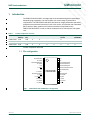
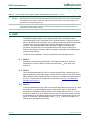
The P89LPC9331/9341/9351 are single-chip microcontrollers designed for applications
demanding high-integration, low cost solutions over a wide range of performance
requirements. The P89LPC9331/9341/9351 are based on a high performance processor
architecture that executes instructions in two to four clocks, six times the rate of standard
80C51 devices. Many system-level functions have been incorporated into the
P89LPC9331/9341/9351 in order to reduce component count, board space, and system
cost.
D
D
R
A
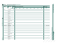
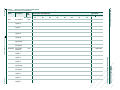
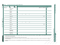
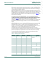
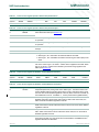
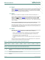
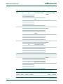
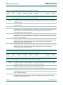
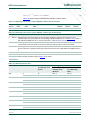
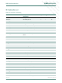
Sector
size
ADC1
ADC0
PGA0
PGA1
Temp
Sensor
CCU
DATA
EEPROM
P89LPC9331
4 kB
1 kB
X
X
-
-
X
-
-
P89LPC9341
4 kB
1 kB
X
X
-
-
X
-
-
P89LPC9351
8 kB
1 kB
X
X
X
X
X
X
X
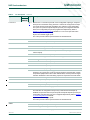
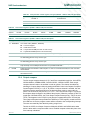
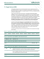
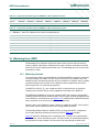
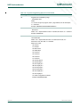
Product Comparison Overview
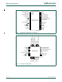
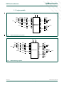
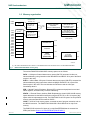
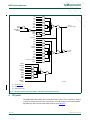
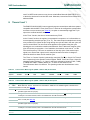
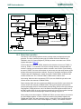
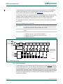
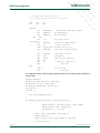
1.1 Pin configuration
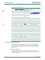
P2.0/AD03/DAC0
1
28 P2.7
P2.1/AD02
2
27 P2.6
P0.0/CMP2/KBI0/AD01
3
26 P0.1/CIN2B/KBI1/AD10
P1.7/AD00
4
25 P0.2/CIN2A/KBI2/AD11
P1.6
5
24 P0.3/CIN1B/KBI3/AD12
P1.5/RST
6
23 P0.4/CIN1A/KBI4/DAC1/AD13
VSS
7
P3.1/XTAL1
8
P3.0/XTAL2/CLKOUT
9
P89LPC9331FDH/
P89LPC9341FDH
22 P0.5/CMPREF/KBI5
21 VDD
20 P0.6/CMP1/KBI6
P1.4/INT1 10
19 P0.7/T1/KBI7
P1.3/INT0/SDA 11
18 P1.0/TXD
P1.2/T0/SCL 12
17 P1.1/RXD
P2.2/MOSI 13
16 P2.5/SPICLK
P2.3/MISO 14
15 P2.4/SS
002aae462
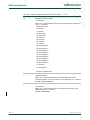
Fig 1.
P89LPC9331/9341 TSSOP28 pin configuration
<Document ID>
User manual
© NXP B.V. 2009. All rights reserved.
Rev. 01.xx — 5 February 2009
3 of 172
A
Flash
Memory
R
Device
D
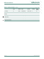
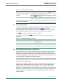
Product comparison overview
FT
Table 1.