Download Giga-tronics ASCOR Model 3000
Transcript
User Manual 96000340
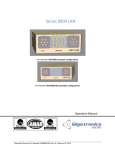
Model 3000-2xxxx
Model 3000-2xxxx
Microwave Relay Carrier
90400340
Page 1
Operation Manual
User Manual 96000340
Model 3000-2xxxx
All technical data and specifications in this publication are subject to change without prior notice and do
not represent a commitment on the part of Giga-tronics, Incorporated.
© 2011 Giga-tronics Incorporated. All rights reserved. Printed in the U.S.A.
Warranty
Giga-tronics Series 3000 Switching Modules are warranted against
defective materials and workmanship for three years from date of shipment,
or as detailed in the warranty section of this manual. Giga-tronics will, at its
option, repair or replace products that are proven defective during the
warranty period. This warranty DOES NOT cover damage resulting from
improper use, nor workmanship other than Giga-tronics service. There is no
implied warranty of fitness for a particular purpose, nor is Giga-tronics liable
for any consequential damages. Specification and price change privileges are
reserved by Giga-tronics.
CONTACT INFORMATION
Giga-tronics, Incorporated
4650 Norris Canyon Road
San Ramon, California 94583
Telephone:
800.726.4442 (only within the United States)
925.328.4650
Fax:
925.328.4700
On the Internet:
www.gigatronics.com
Page 2
Operation Manual
User Manual 96000340
Model 3000-2xxxx
Regulatory compliance information
This product complies with the essential requirements of the following applicable European
Directives, and carries the CE mark accordingly.
89/336/EEC and 73/23/EEC
EMC Directive and Low Voltage Directive
EN61010-1 (1993)
Electrical Safety
EN61326-1 (1997)
EMC – Emissions and Immunity
Manufacturer’s Name:
Manufacturer’s Address
Giga-tronics, Incorporated
4650 Norris Canyon Road
San Ramon, California 94583
U.S.A.
Type of Equipment:
Model Series Number
Switching Module
3000-2xxxx
Declaration of Conformity on file. Contact Giga-tronics at the following;
Giga-tronics, Incorporated
4650 Norris Canyon Road
San Ramon, California 94583
Telephone:
800.726.4442 (only within the United States)
925.328.4650
Fax:
925.328.4700
Page 3
Operation Manual
User Manual 96000340
Model 3000-2xxxx
Record of Changes to This Manual
Use the table below to maintain a permanent record of changes to this document. Corrected
replacement pages are issued as Technical Publication Change Instructions (TPCI). When you
are issued a TPCI, do the following:
1. Insert the TPCI at the front of the manual binder.
2. Remove the pages from the manual binder that are noted in the TPCI.
3. Replace the page(s) removed in the previous step with the corrected page(s).
4. Record the changes in the table below.
TPCI
Number
TPCI Issue
Date
Date Entered
Comments
Page 4
Operation Manual
User Manual 96000340
Model 3000-2xxxx
Revision History
Revision
A
B
C
Description of Change
Initial Release
Updated
Reformatted 3/12
Chg Order #
Approved By
RCW
Page 5
Operation Manual
User Manual 96000340
Model 3000-2xxxx
Contents
Contents ........................................................................................................................................................ 6
Chapter 1 Introduction ................................................................................................................................. 7
1.1 Safety and Manual Conventions ......................................................................................................... 7
1.1.1 Product Reference....................................................................................................................... 7
1.1.2 Personal Safety Alert ................................................................................................................... 7
1.1.3 Equipment Safety Alert ............................................................................................................... 7
1.1.4 Notes ........................................................................................................................................... 7
1.1.5 Electrical Safety Precautions ....................................................................................................... 7
Chapter 2 Configuration Table ...................................................................................................................... 8
Chapter 3 Functional Description ................................................................................................................. 9
3.1 Introduction ........................................................................................................................................ 9
3.2 General Description ............................................................................................................................ 9
Chapter 4 Controls and Indicators .............................................................................................................. 10
4.1 VXI Logical Address ........................................................................................................................... 10
4.2 LEDs................................................................................................................................................... 10
4.2.1 “BUS” LED .................................................................................................................................. 10
4.2.2 “PWR” LED ................................................................................................................................. 10
Chapter 5 Internal Settings ......................................................................................................................... 11
5.1 Fuse................................................................................................................................................... 11
5.2 VXIbus Interrupt Level Selection......................................................................................................... 11
Chapter 6 Specifications ............................................................................................................................. 12
Chapter 8 Register Map .............................................................................................................................. 14
8.1 REGISTER MAP – 16 BIT ASSIGNMENTS ........................................................................................... 15
8.2 REGISTER MAP – 32 BIT ASSIGNMENTS ........................................................................................... 17
Page 6
Operation Manual
User Manual 96000340
Model 3000-2xxxx
Chapter 1 Introduction
1.1 Safety and Manual Conventions
This manual contains conventions regarding safety and equipment usage as described below.
1.1.1 Product Reference
Throughout this manual, the term “Common Core Switching Platform, Series 8800” refers to all models
of within the series, unless otherwise specified.
1.1.2 Personal Safety Alert
WARNING: Indicates a hazardous situation which, if not avoided, could result in
WARNING
death or serious injury.
!
1.1.3 Equipment Safety Alert
CAUTION CAUTION: Indicates a situation which can damage or adversely affect the product or
associated equipment.
1.1.4 Notes
Notes are denoted and used as follows:
NOTE: Highlights or amplifies an essential operating or maintenance procedure, practice, condition or
statement.
1.1.5 Electrical Safety Precautions
Any servicing instructions are for use by service-trained personnel only. To avoid personal injury, do not
perform any service unless you are qualified to do so.
For continued protections against fire hazard, replace the AC line fuse only with a fuse of the same
current rating and type. Do not use repaired fuses or short circuited fuse holders.
Page 7
Operation Manual
User Manual 96000340
Model 3000-2xxxx
Chapter 2 Configuration Table
Basic RF Module
MAXIMUM CONFIGURATION
VXI
Width
90400340
Six 1x6 RF Switches
2
90400350
Twelve 1x6 RF Switches
3
90400730
Four 1x6 RF Switches ( TERM )
2
90400950
Three 1x6 TERM & Three SPDT, TERM
2
90400720
Eight 1x6, TERM.
4
90401080
Six 1x6, TERM & Six SPDT, TERM
4
90400580
Eight 1x6, TERM & Three SPDT, TERM.
5
9040350-003
Five 1x6, Non-Term, Two SPDT, Non-Term, One 1x6, Term, Two SPDT,
Term
3
90401470
Fifteen 1x6 RF Switches
4
90401470-100
Ten 1x6 RF Switches, & Five Transfer RF Switches
4
WITHOUT
RF Switches
Page 8
Operation Manual
User Manual 96000340
Model 3000-2xxxx
Chapter 3 Functional Description
3.1 Introduction
This manual provides basic information for the operation and maintenance of the Series 3000-2xxxx VXI
Modules.
3.2 General Description
The Series 3000-2xx is a collection of standard VXI modules that have a variety of configurations of RF
Switches. Consult the Configuration List at the back of the manual to see our present standard ( COTS )
products.
Our present standard offering of RF Switches is 1x6 and SPDT, 26.5GHz, Non-Terminated and 1x6 and
SPDT, 18.0 GHz, Terminated. Other switch units such as 1x8, Transfer switches and bandwidths up to 40
GHz can also be accommodated.
One of the unique features of the Series 3000-2xx RF Modules is that the RF Switches can be removed
and replaced from the front of the unit. This allows quick replacement for maintenance or reconfiguration without requiring the complete removal of the VXI Module.
Another feature is that all VXI RF Modules are Configurable. This means that for any particular module
you can have as many or as few RF Switches as you want, in any arrangement , for your unique
application.
While the Configuration List shows the products that presently exist in our inventory, custom
configurations can easily be developed since changes would primarily involve the Front Panel. The
internal electronic circuits and VXI interface would remain the same. Any device that can be operated by
a programmed bit and mounted on the front panel ( such as Optical Switches) can be accommodated.
Consult with the factory if you have particular needs.
Page 9
Operation Manual
User Manual 96000340
Model 3000-2xxxx
Chapter 4 Controls and Indicators
The following controls and indicators are provided to select and display the functions of the ASCOR
3000-2xxxx Module’s operating environment.
4.1 VXI Logical Address
The Logical Address Switch is dual circular switches, D1 and D2 which are located at the rear of the
module. The address can be set to any value between 1 and 255 (decimal) or 1 and FF (hexadecimal),
(address 0 is reserved for the resource manager). However, the Module fully supports Dynamic
Configuration as defined in Section F of the VXI specification, address 255 (FF) should be selected only if
the Resource Manager also supports Dynamic Configuration.
4.2 LEDs
The following LEDs are visible at the Module’s front panel to indicate the
status of the module’s operation:
4.2.1 “BUS” LED
This green color LED is normally off and will flash on when the module is addressed by the system.
4.2.2 “PWR” LED
This red color LED is normally on when the Module is Powered up.
Page 10
Operation Manual
User Manual 96000340
Model 3000-2xxxx
Chapter 5 Internal Settings
The following items are inside the module and can be reached by removing the side cover.
5.1 Fuse
The ASCOR VXI 3000-2xxxx uses a 10 Amp fuse in the +5 Volt line and is located on
the Mother Board (MB) assembly.
5.2 VXIbus Interrupt Level Selection
The VXIbus interrupt level is set with three bits in the “3Eh” register.
See the section on “A16 ADDRESS SPACE REGISTER DESCRIPTION”.
The interrupt level is factory set to “no interrupt”.
Page 11
Operation Manual
User Manual 96000340
Model 3000-2xxxx
Chapter 6 Specifications
RF Switches – General Characteristics, other Relays available upon Request
1x6 Non-Terminated ( p/n 52200020 )
Frequency ( GHz )
DC - 3
VSWR
( MAX )
1.20 : 1
Insertion Loss ( MAX )
0.20 dB
Isolation
>=
80 dB
Average Power
(*)
120 W
Characteristic Impedance :
Switching Time (nominal @ 25º C )
Actuation Voltage :
Connectors :
Life Expectancy :
Operation Mode :
3-8
8 -12.4
1.30 : 1
1.40 : 1
0.30 dB
0.40 dB
70 dB
60 dB
80 W
60 W
50 Ohms
< 10 ms
12 VDC @ 250 ma
SMA Female
5,000,000 cycles per position
All positions Open at Reset
12.4 -18
1.50 : 1
0.50 dB
60 dB
50 W
18 – 26.5
1.60 : 1
0.60 dB
55 dB
30 W
SPDT Non-Terminated ( p/n 52200120 )
Frequency ( GHz )
DC - 3
VSWR (MAX)
1.20 : 1
Insertion Loss ( MAX )
0.20 dB
Isolation
>= 80 dB
Average Power
(*) 120 W
3-8
1.30 : 1
0.30 dB
70 dB
80 W
12.4 -18
1.50 : 1
0.50 dB
60 dB
50 W
18 – 26.5
1.60 : 1
0.60 dB
55 dB
30 W
Characteristic Impedance :
Switching Time (nominal @ 25º C )
Actuation Voltage :
Connectors :
Life Expectancy :
Operation Mode :
1x6 Terminated ( p/n 52200060 )
Frequency ( GHz )
DC - 3
VSWR ( MAX )
1.20 : 1
Isolation ( MAX )
80 dB
Insertion Loss ( dB )
0.20 dB
Average Power
(*)
120 W
Characteristic Impedance :
Switching Time (nominal @ 25º C )
Actuation Voltage :
Connectors :
Life Expectancy :
Operation Mode :
8 -12.4
1.40 : 1
0.40 dB
60 dB
60 W
50 Ohms
< 10 ms
12 VDC @ 160ma
SMA Female
10,000,000 cycles
Failsafe
(1)
3-8
8-16
1.30 : 1
1.40 : 1
70 dB
60 dB
0.30 dB
0.40 dB
80 W
60 W
50 Ohms
< 15 ms
12 VDC @ 680ma
SMA Female
1,000,000 cycles
Terminated at Reset
16-18
1.50 : 1
60 dB
0.50 dB
50 W
Page 12
Operation Manual
User Manual 96000340
Model 3000-2xxxx
SPDT Terminated ( p/n 52200040 )
(1)
Frequency ( GHz )
DC - 3
VSWR ( MAX )
1.20 : 1
Isolation ( MAX )
80 dB
Insertion Loss ( dB )
0.20 dB
Average Power
(*)
120 W
Characteristic Impedance :
Switching Time (nominal @ 25º C )
Actuation Voltage :
Connectors :
Life Expectancy :
Operation Mode :
3-8
8-16
16-18
1.30 : 1
1.40 : 1
1.50 : 1
70 dB
60 dB
60 dB
0.30 dB
0.40 dB
0.50 dB
80 W
60 W
50 W
50 Ohms
< 20 ms
12 VDC @ 680ma
SMA Female
1,000,000 cycles
At Reset : NC -> C ; NO Terminated
( * ) = average Power a 25º C per RF Path
( 1 ) = CAUTION : Termination Resistors have a MAXIMUM Power rating of 2 Watt.
Mechanical:
The VXI RF modules come in various standard VXI widths. Some are 2-wide, 3-wide , 4-wide or 5-wide.
The Depth and the Height are per the VXI Standard. The Widths are multiplies of the standard VXI 1wide modules. See the Configuration List for the Width of any particular module.
2-WIDE
2.4 inches
10.317 inches
13.78 inches
WIDTH
HEIGHT
DEPTH
Weight
3-WIDE
3.6 inches
10.317 inches
13.78 inches
4-WIDE
4.8 inches
10.317 inches
13.78 inches
5-WIDE
6.0 inches
10.317 inches
13.78 inches
3 to 8 lbs depending on configuration
Environmental Specifications
Temperature:
Operating:
0º to 55ºC
Storage:
- 40º to 75ºC
Relative Humidity:
Operating:
0 to 90% non-condensing
Storage:
0 to 95% non-condensing
Page 13
Operation Manual
User Manual 96000340
Model 3000-2xxxx
Chapter 8 Register Map
Programming of the Model 3000-2xx is very straight forward. The module is organized into eight sixteen
bit registers. Each register supports 16 coil drivers in 16 BIT Mode or two 16 bit registers support 32 coil
drivers in 32 BIT Mode.
For example, the lower eight bits ( bits 0-7 ) of the first register control the first switch SW1.
The upper eight bits ( 8-15 ) controls the second switch SW2.
The lower eight bits ( bits 0-7 ) of the second register controls SW3.
The upper eight bits ( 8-15 ) controls SW4.
This configuration is carried through the complete module.
Register Map – 16 Bit Configuration
A16 Register
Offset
Value
00h
CFB5
7 = Register Based, A16,/A24 Module
FB5 = VXI Manufacturer ID, ASCOR
02h
7FCC ( for 3000-2xx )
7 = A24 space requirement
FCC – Model Number for this Module
04h
FFFCh
Bit 0, reset, is supported.
Toggling this bit will clear all relay registers
06G
( Assigned by Resource Manager )
Control Bit
3Eh
0
1
Low true output enable to the coil driver IC’s
When low, enables read back of the coil state.
When high, enables read back of the data registers.
NOTE : There is no data register read back for this module. Always clear this bit low.
2
Always set LOW. ( Reserved for factory use only )
3-15
Don’t Care Bits
Page 14
Operation Manual
User Manual 96000340
Model 3000-2xxxx
8.1 REGISTER MAP – 16 BIT ASSIGNMENTS
ADDRESS OFFSET = 40h
MSB
LSB
Register Bit
15
14
13
12
11
10
9
8
7
6
5
4
3
2
1
0
SW - Contact
2-8
2-7
2-6
2-5
2-4
2-3
2-2
2-1
1-8
1-7
1-6
1-5
1-4
1-3
1-2
1-1
ADDRESS OFFSET = 42h
MSB
LSB
Register Bit
15
14
13
12
11
10
9
8
7
6
5
4
3
2
1
0
SW - Contact
4-8
4-7
4-6
4-5
4-4
4-3
4-2
4-1
3-8
3-7
3-6
3-5
3-4
3-3
3-2
3-1
ADDRESS OFFSET = 44h
MSB
LSB
Register Bit
15
14
13
12
11
10
9
8
7
6
5
4
3
2
1
0
SW - Contact
6-8
6-7
6-6
6-5
6-4
6-3
6-2
6-1
5-8
5-7
5-6
5-5
5-4
5-3
5-2
5-1
ADDRESS OFFSET = 46h
MSB
LSB
Register Bit
15
14
13
12
11
10
9
8
7
6
5
4
3
2
1
0
SW - Contact
8-8
8-7
8-6
8-5
8-4
8-3
8-2
8-1
7-8
7-7
7-6
7-5
7-4
7-3
7-2
7-1
ADDRESS OFFSET = 48h
MSB
Register Bit
SW - Contact
LSB
15
14
13
12
11
10
9
8
7
6
5
4
3
2
1
0
10-8
10-7
10-6
10-5
10-4
10-3
10-2
10-1
9-8
9-7
9-6
9-5
9-4
9-3
9-2
9-1
ADDRESS OFFSET = 4Ah
MSB
LSB
Register Bit
15
14
13
12
11
10
9
8
7
6
5
4
3
2
1
0
SWContact
12-8
12-7
12-6
12-5
12-4
12-3
12-2
12-1
11-8
11-7
11-6
11-5
11-4
11-3
11-2
11-1
Page 15
Operation Manual
User Manual 96000340
Model 3000-2xxxx
ADDRESS OFFSET = 4Ch
MSB
Register Bit
SW - Contact
LSB
15
14
13
12
11
10
9
8
7
6
5
4
3
2
1
0
14-8
14-7
14-6
14-5
14-4
14-3
14-2
14-1
13-8
13-7
13-6
13-5
13-4
13-3
13-2
13-1
ADDRESS OFFSET = 4Eh
MSB
Register Bit
SW - Contact
LSB
15
14
13
12
11
10
9
8
7
6
5
4
3
2
1
0
16-8
16-7
16-6
16-5
16-4
16-3
16-2
16-1
15-8
15-7
15-6
15-5
15-4
15-3
15-2
15-1
SW = Switch designation
Contact = Switch Contact
Page 16
Operation Manual
User Manual 96000340
Model 3000-2xxxx
8.2 REGISTER MAP – 32 BIT ASSIGNMENTS
ADDRESS OFFSET = 40h
LSB
Register Bit
15
14
13
12
11
10
9
8
7
6
5
4
3
2
1
0
SW - Contact
2-8
2-7
2-6
2-5
2-4
2-3
2-2
2-1
1-8
1-7
1-6
1-5
1-4
1-3
1-2
1-1
MSB
Register Bit
31
30
29
28
27
26
25
24
23
22
21
20
19
18
17
16
SW - Contact
4-8
4-7
4-6
4-5
4-4
4-3
4-2
4-1
3-8
3-7
3-6
3-5
3-4
3-3
3-2
3-1
ADDRESS OFFSET = 44h
LSB
Register Bit
15
14
13
12
11
10
9
8
7
6
5
4
3
2
1
0
SW - Contact
6-8
6-7
6-6
6-5
6-4
6-3
6-2
6-1
5-8
5-7
5-6
5-5
5-4
5-3
5-2
5-1
MSB
Register Bit
31
30
29
28
27
26
25
24
23
22
21
20
19
18
17
16
SW - Contact
8-8
8-7
8-6
8-5
8-4
8-3
8-2
8-1
7-8
7-7
7-6
7-5
7-4
7-3
7-2
7-1
ADDRESS OFFSET = 48h
LSB
Register Bit
SW - Contact
15
14
13
12
11
10
9
8
7
6
5
4
3
2
1
0
10-8
10-7
10-6
10-5
10-4
10-3
10-2
10-1
9-8
9-7
9-6
9-5
9-4
9-3
9-2
9-1
MSB
Register Bit
31
30
29
28
27
26
25
24
23
22
21
20
19
18
17
16
SWContact
12-8
12-7
12-6
12-5
12-4
12-3
12-2
12-1
11-8
11-7
11-6
11-5
11-4
11-3
11-2
11-1
ADDRESS OFFSET = 4Ch
LSB
Register Bit
SW - Contact
15
14
13
12
11
10
9
8
7
6
5
4
3
2
1
0
14-8
14-7
14-6
14-5
14-4
14-3
14-2
14-1
13-8
13-7
13-6
13-5
13-4
13-3
13-2
13-1
31
30
29
28
27
26
25
24
23
22
21
20
19
18
17
16
16-8
16-7
16-6
16-5
16-4
16-3
16-2
16-1
15-8
15-7
15-6
15-5
15-4
15-3
15-2
15-1
MSB
Register Bit
SW - Contact
SW = Switch designation
Contact = Switch Contact
Page 17
Operation Manual


