1
POLITECNICO DI MILANO
Scuola di Ingegneria Industriale
Corso di Laurea Magistrale in Ingegneria Aeronautica
Design and development of the new generation of the
"Mnemosine" FTI system for light aircraft
Relatore: prof. Alberto ROLANDO
Tesi di Laurea di:
Federico ROSSI
Matr. 763665
Anno Accademico 2011/2012
Sommario
Questa tesi nasce per rispondere alla richiesta di una nuova generazione di strumentazione
per prove di volo per velivoli ultraleggeri sviluppata dal Dipartimento di Scienze e Tecnologie Aerospaziali del Politecnico di Milano. Tale strumentazione andrà a sostituire la precedente
versione chiamata Mnemosine MK III che essenzialmente si compone di più case metallici contenenti i nodi, ognuno con le proprie caratteristiche, che comunicano fra loro tramite protocollo
Controller Area Network (CAN) data bus appositamente sviluppato.
Quanto segue è il risultato di diverse analisi volte allo sviluppo del nuovo sistema ight test
instrumentation (FTI) chiamato Mnemosine MK IV. Capitalizzando i progressi dell'industria
dei semiconduttori, questa nuova versione introduce l'integrazione di più nodi in un'unica unità
centrale, le cui funzioni sono governate da un sistema operativo real-time.
Fin da subito si espone la volontà di utilizzare il più possibile software e codici sorgenti Open
Source.
Il lavoro qui presentato è composto da una parte introduttiva, dove si riporta brevemente la
storia dell'evoluzione di Mnemosine con una parentesi rivolta al mondo dell'aviazione, la ricerca
formale dei nuovi requisiti raccolti durante le campagne di ight test sia in ambito accademico sia
in ambito aziendale grazie al progetto Poli-XFlight. Segue il progetto di massima dell'hardware,
che in alcuni casi si spingerà più in dettaglio secondo le esigenze funzionali e la descrizione della
losoa software no alla redazione della specica dei requisiti e la presentazione dei codici di
validazione realizzati con lo scopo di vericare l'eettiva fattibilità dell'intero progetto.
i
Abstract
This thesis was created to meet the demand for a new generation of ight test instrumentation
for ultra-light aircraft developed by the Dipartimento di Scienze e Tecnologie Aerospaziali of
Politecnico di Milano. This instrumentation will replace the previous version called Mnemosine
MK III which essentially consists of several metal cases containing nodes, each one with its own
characteristics, which communicate with each other through a specially developed protocol based
on Controller Area Network (CAN).
What follows is the result of several analysis aimed at developing the new ight test instrumentation (FTI) system called Mnemosine MK IV. Thanks to the progress of the semiconductor
industry, this new version introduces the integration of multiple nodes in a single central unit,
whose operations are governed by a real time operating system.
Right from the start it exposes the desire to use as much as possible Open Source software
and source code.
This work consists of an introduction, where is given a brief history of general ight test activity
and the evolution of Mnemosine, the formal research of new requirements gathered during the
ight test campaigns both in academic and in business through to the project Poli-XFlight.
Follows the hardware preliminary design, that in some cases goes into detail according to the
functional requirements. Then the description of the software philosophy until the preparation
of the requirements specication and the presentation of the demo made with the purpose of
verifying the actual feasibility of entire project.
iii
Contents
Abstract
iii
Contents
v
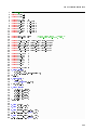
List of Figures
ix
List of Tables
xi
List of Acronyms
xiii
1 Introduction
1
1.1
A bit of FTI history...
. . . . . . . . . . . . . . . . . . . . . . . . . . . . . . . . .
1
1.1.1
Data Acquisition Methods . . . . . . . . . . . . . . . . . . . . . . . . . . .
2
1.1.2
Data Processing and Analysis Methods
. . . . . . . . . . . . . . . . . . .
3
. . . . . . . . . . . . . . . . . . . . . . . . . . . . . .
4
. . . . . . . . . . . . . . . . . . . . . . . . . . . . . . . . . . . . . . . . . .
5
1.3.1
CS-VLA . . . . . . . . . . . . . . . . . . . . . . . . . . . . . . . . . . . . .
5
1.3.2
CS-LSA . . . . . . . . . . . . . . . . . . . . . . . . . . . . . . . . . . . . .
5
1.4
ULM Regulation in Italy . . . . . . . . . . . . . . . . . . . . . . . . . . . . . . . .
7
1.5
History of Mnemosine FTI . . . . . . . . . . . . . . . . . . . . . . . . . . . . . . .
8
1.5.1
Initial requirements . . . . . . . . . . . . . . . . . . . . . . . . . . . . . . .
8
1.5.2
Actual state: Mnemosine MK III . . . . . . . . . . . . . . . . . . . . . . .
9
1.2
ULM Ultra Light Machine
1.3
EASA
1.6
Operating limits
. . . . . . . . . . . . . . . . . . . . . . . . . . . . . . . . . . . .
1.7
Upgrade requirements
. . . . . . . . . . . . . . . . . . . . . . . . . . . . . . . . .
2 Hardware Realization
2.1
Development board
2.1.1
10
11
13
. . . . . . . . . . . . . . . . . . . . . . . . . . . . . . . . . .
15
STM32F407 . . . . . . . . . . . . . . . . . . . . . . . . . . . . . . . . . . .
15
2.2
Power Supply Section
. . . . . . . . . . . . . . . . . . . . . . . . . . . . . . . . .
17
2.3
Multi-Mode Serial Peripheral Interface . . . . . . . . . . . . . . . . . . . . . . . .
18
2.4
Analog Signal Conditioning Module . . . . . . . . . . . . . . . . . . . . . . . . . .
21
2.4.1
Noise Filter . . . . . . . . . . . . . . . . . . . . . . . . . . . . . . . . . . .
21
2.4.2
Schematics of Analog Signal Conditioning Module
. . . . . . . . . . . . .
22
2.4.3
PCB . . . . . . . . . . . . . . . . . . . . . . . . . . . . . . . . . . . . . . .
22
Secure Digital Card . . . . . . . . . . . . . . . . . . . . . . . . . . . . . . . . . . .
24
2.5.1
. . . . . . . . . . . . . . . . . . . . . . . . . . . . . . . . . .
25
Air Data Computer . . . . . . . . . . . . . . . . . . . . . . . . . . . . . . . . . . .
26
2.5
2.6
SPI vs SDIO
v
CONTENTS
2.7
Engine Data . . . . . . . . . . . . . . . . . . . . . . . . . . . . . . . . . . . . . . .
27
2.8
Stick Force Data
. . . . . . . . . . . . . . . . . . . . . . . . . . . . . . . . . . . .
27
2.9
Inertial Data
. . . . . . . . . . . . . . . . . . . . . . . . . . . . . . . . . . . . . .
29
2.10 GPS Data . . . . . . . . . . . . . . . . . . . . . . . . . . . . . . . . . . . . . . . .
30
2.11 CDU (Command and Display Unit) . . . . . . . . . . . . . . . . . . . . . . . . . .
31
3 Software Realization
3.1
Real Time Operating System
33
. . . . . . . . . . . . . . . . . . . . . . . . . . . . .
33
. . . . . . . . . . . . . . . . . . . . . . . . . . . . . .
34
3.2
Development Environment . . . . . . . . . . . . . . . . . . . . . . . . . . . . . . .
36
3.3
Thread denitions (High Level Software Requirements) . . . . . . . . . . . . . . .
37
3.3.1
Main . . . . . . . . . . . . . . . . . . . . . . . . . . . . . . . . . . . . . . .
38
3.3.2
Time scheduler . . . . . . . . . . . . . . . . . . . . . . . . . . . . . . . . .
38
3.3.3
SD thread . . . . . . . . . . . . . . . . . . . . . . . . . . . . . . . . . . . .
39
3.3.4
Ethernet thread . . . . . . . . . . . . . . . . . . . . . . . . . . . . . . . . .
40
3.3.5
CAN thread . . . . . . . . . . . . . . . . . . . . . . . . . . . . . . . . . . .
40
3.3.6
GPS thread . . . . . . . . . . . . . . . . . . . . . . . . . . . . . . . . . . .
41
3.3.7
Stick force thread . . . . . . . . . . . . . . . . . . . . . . . . . . . . . . . .
41
3.3.8
AHRS thread . . . . . . . . . . . . . . . . . . . . . . . . . . . . . . . . . .
42
3.3.9
CDU thread . . . . . . . . . . . . . . . . . . . . . . . . . . . . . . . . . . .
43
3.1.1
Choosing the RTOS
3.3.10 Control surface position thread
3.4
. . . . . . . . . . . . . . . . . . . . . . . .
43
3.3.11 Air thread . . . . . . . . . . . . . . . . . . . . . . . . . . . . . . . . . . . .
44
Software Requirements Specication (SRS)
45
. . . . . . . . . . . . . . . . . . . . .
4 Hardware & Software Suitability Validation Code
47
4.1
Serial Driver SVC . . . . . . . . . . . . . . . . . . . . . . . . . . . . . . . . . . . .
48
4.2
USART/UART SVC . . . . . . . . . . . . . . . . . . . . . . . . . . . . . . . . . .
49
4.3
Analog to Digital Converter SVC . . . . . . . . . . . . . . . . . . . . . . . . . . .
50
4.4
SD SDIO Mode SVC . . . . . . . . . . . . . . . . . . . . . . . . . . . . . . . . . .
52
4.5
Time Scheduler SVC . . . . . . . . . . . . . . . . . . . . . . . . . . . . . . . . . .
53
4.6
Input Capture SVC . . . . . . . . . . . . . . . . . . . . . . . . . . . . . . . . . . .
55
4.7
CAN SVC . . . . . . . . . . . . . . . . . . . . . . . . . . . . . . . . . . . . . . . .
56
4.8
I C SVC . . . . . . . . . . . . . . . . . . . . . . . . . . . . . . . . . . . . . . . . .
57
²
5 Conclusion and Future Developments
59
5.1
Prototyping . . . . . . . . . . . . . . . . . . . . . . . . . . . . . . . . . . . . . . .
59
5.2
Conclusion . . . . . . . . . . . . . . . . . . . . . . . . . . . . . . . . . . . . . . . .
59
Bibliography
61
Appendix A (SRS)
63
vi
CONTENTS
Appendix B (SVC)
91
Serial Driver source code . . . . . . . . . . . . . . . . . . . . . . . . . . . . . . . . . . .
91
USART/UART Driver source code . . . . . . . . . . . . . . . . . . . . . . . . . . . . .
92
ADC Driver source code . . . . . . . . . . . . . . . . . . . . . . . . . . . . . . . . . . .
94
SDIO Driver source code . . . . . . . . . . . . . . . . . . . . . . . . . . . . . . . . . . .
96
Time Scheduler source code . . . . . . . . . . . . . . . . . . . . . . . . . . . . . . . . .
98
IC Driver source code
. . . . . . . . . . . . . . . . . . . . . . . . . . . . . . . . . . . .
106
CAN Driver source code . . . . . . . . . . . . . . . . . . . . . . . . . . . . . . . . . . .
108
I C Driver source code . . . . . . . . . . . . . . . . . . . . . . . . . . . . . . . . . . . .
110
²
Appendix C (ChibiStudio)
113
Appendix D (Software Upgrade Procedures)
115
JTAG
. . . . . . . . . . . . . . . . . . . . . . . . . . . . . . . . . . . . . . . . . . . . .
115
UART . . . . . . . . . . . . . . . . . . . . . . . . . . . . . . . . . . . . . . . . . . . . .
118
vii
List of Figures
1.1
Block diagram of Mnemosine MK III . . . . . . . . . . . . . . . . . . . . . . . . .
1.2
Mnemosine MK III installed on board
. . . . . . . . . . . . . . . . . . . . . . . .
10
2.1
Mnemosine MK IV . . . . . . . . . . . . . . . . . . . . . . . . . . . . . . . . . . .
13
2.2
Mnemosine MK IV Rendering
. . . . . . . . . . . . . . . . . . . . . . . . . . . .
14
2.3
STM32E407 Layout
. . . . . . . . . . . . . . . . . . . . . . . . . . . . . . . . . .
16
2.4
Power Supply Diagram . . . . . . . . . . . . . . . . . . . . . . . . . . . . . . . . .
17
2.5
Conceptual diagram of multi-mode serial peripheral interface
. . . . . . . . . . .
19
2.6
Noise Filter schematic
. . . . . . . . . . . . . . . . . . . . . . . . . . . . . . . . .
21
2.7
Schematics of Analog Signal Conditioning Module
. . . . . . . . . . . . . . . . .
22
2.8
PCB of Analog Signal Conditioning Module . . . . . . . . . . . . . . . . . . . . .
23
2.9
3D PCB of Analog Signal Conditioning Module . . . . . . . . . . . . . . . . . . .
23
2.10 SPI vs SDIO
9
. . . . . . . . . . . . . . . . . . . . . . . . . . . . . . . . . . . . . .
25
2.11 HCLA Pressure Sensors Family . . . . . . . . . . . . . . . . . . . . . . . . . . . .
26
2.12 Typical Hall eect sensor and type J thermocouple . . . . . . . . . . . . . . . . .
27
2.13 Futek MU300 . . . . . . . . . . . . . . . . . . . . . . . . . . . . . . . . . . . . . .
27
2.14 Mantracourt DSC Load Cell Embedded Digitiser
. . . . . . . . . . . . . . . . . .
28
2.15 Xsens MTi . . . . . . . . . . . . . . . . . . . . . . . . . . . . . . . . . . . . . . . .
29
2.16 U-Blox LEA-XT
. . . . . . . . . . . . . . . . . . . . . . . . . . . . . . . . . . . .
30
2.17 CDU Rendering
. . . . . . . . . . . . . . . . . . . . . . . . . . . . . . . . . . . .
31
3.1
ChibiStudio screen shot
. . . . . . . . . . . . . . . . . . . . . . . . . . . . . . . .
36
3.2
SDC diagram
. . . . . . . . . . . . . . . . . . . . . . . . . . . . . . . . . . . . . .
39
3.3
CAN diagram . . . . . . . . . . . . . . . . . . . . . . . . . . . . . . . . . . . . . .
41
3.4
SD driver
41
3.5
UART driver
. . . . . . . . . . . . . . . . . . . . . . . . . . . . . . . . . . . . . .
42
3.6
UART driver transmission diagram . . . . . . . . . . . . . . . . . . . . . . . . . .
42
3.7
UART driver receiver diagram . . . . . . . . . . . . . . . . . . . . . . . . . . . . .
42
3.8
ADC driver
. . . . . . . . . . . . . . . . . . . . . . . . . . . . . . . . . . . . . . .
43
3.9
I C driver . . . . . . . . . . . . . . . . . . . . . . . . . . . . . . . . . . . . . . . .
44
²
. . . . . . . . . . . . . . . . . . . . . . . . . . . . . . . . . . . . . . . .
3.10 Overall Software Conguration Flowchart
. . . . . . . . . . . . . . . . . . . . . .
45
4.1
Serial Driver SVC Flowchart
. . . . . . . . . . . . . . . . . . . . . . . . . . . . .
48
4.2
USART/UART Driver SVC Flowchart . . . . . . . . . . . . . . . . . . . . . . . .
49
4.3
ADC Driver SVC Flowchart
. . . . . . . . . . . . . . . . . . . . . . . . . . . . .
51
4.4
SDIO Driver SVC Flowchart . . . . . . . . . . . . . . . . . . . . . . . . . . . . . .
52
ix
LIST OF FIGURES
x
4.5
Time Scheduler SVC Flowchart . . . . . . . . . . . . . . . . . . . . . . . . . . . .
53
4.6
Input Capture SVC Flowchart . . . . . . . . . . . . . . . . . . . . . . . . . . . . .
55
4.7
CAN Driver SVC Flowchart . . . . . . . . . . . . . . . . . . . . . . . . . . . . . .
56
4.8
I C Driver SVC Flowchart . . . . . . . . . . . . . . . . . . . . . . . . . . . . . . .
57
5.1
Boards Arrangement . . . . . . . . . . . . . . . . . . . . . . . . . . . . . . . . . .
60
5.2
Flash Loader Demonstrator 1
. . . . . . . . . . . . . . . . . . . . . . . . . . . . .
118
5.3
Flash Loader Demonstrator 2
. . . . . . . . . . . . . . . . . . . . . . . . . . . . .
119
5.4
Flash Loader Demonstrator 3
. . . . . . . . . . . . . . . . . . . . . . . . . . . . .
119
5.5
Flash Loader Demonstrator 4
. . . . . . . . . . . . . . . . . . . . . . . . . . . . .
120
5.6
Flash Loader Demonstrator 5
. . . . . . . . . . . . . . . . . . . . . . . . . . . . .
120
²
List of Tables
2.1
Pin conguration of multi-mode serial peripheral interface . . . . . . . . . . . . .
19
2.2
Pin conguration of multi-mode serial peripheral interface . . . . . . . . . . . . .
20
2.3
pad assignment . . . . . . . . . . . . . . . . . . . . . . . . . . . . . . . . . . . . .
24
4.1
ADC board: pin conguration . . . . . . . . . . . . . . . . . . . . . . . . . . . . .
50
xi
List of Acronyms
ADC
Air Data Computer
ADC
Analog To Digital Converter
AHRS
Attitude Heading Reference System
AOA
Angle Of Attack
AOS
Angle Of Sidesleep
API
Application Program Interface
ATZ
Air Trac Zone
CAFFE
CAN for Flight-test Equipment
CAN
Controller Area Network
CAS
Calibrated Air Speed
CCM
Core Coupled Memory
CDU
Command and Display Unit
CPU
Central Processing Unit
CS-LSA
Certication Specication Light Sport Aircraft
CS-VLA
Certication Specication Very Light Aircraft
DAC
Digital Converter To Analog
DMA
Direct Memory Access
DPR
Decreto Presidente della Repubblica
DSP
Digital Signal Processor
EASA
European Aviation Safety Agency
EFIS
Electronic Flight Instrument System
EFIS
Electronic Flight Instruments System
EGT
Exhaust Gas Temperature
EICAS
Engine Indicating and Crew Alerting System
xiii
List of Acronyms
ELT
Emergency Locator Transmitter
FM
Frequency Modulation
FPU
Floating Point Unit
FTE
Flight Test Engineer
FTI
Flight Test Instrumentation
GPIO
General Purpose Input/Output
GPS
Global Positioning System
HAL
Hardware Abstraction Layer
HTTP
Hypertext Transfer Protocol
²
²
I C
Inter-Integrated Circuit
I S
Inter IC Sound
ICMP
Internet Control Message Protocol
IDE
Integrated Development Environment
ISR
Interrupt service routine
JTAG
Joint Test Action Group
lwIP
light-weight Internet Protocol
MCU
Microcontroller Unit
MPU
Memory Protection Unit
MTOW
Maximum Take-o Weight
NetBIOS Network Basic Input/Output System
OPSW
Operational Software
OTG
On The Go USB Peripheral
PCM
Pulse Code Modulation
PLL
Phase-Locked Loop
PPPoE
Point-to-Point Protocol Over Ethernet
PWM
Pulse Width Modulation
RISC
Reduced Instruction Set Code
RMS
Rate Monotonic Scheduling
xiv
List of Acronyms
ROM
Read-Only Memory
RPM
Revolutions Per Minute
RTOS
Real Time Operating System
RTT
Round-Trip Time
SBAS
Satellite-Based Augmentation System
SDC
Secure Digital Card
SDIO
Secure Digital Input/Output
SRAM
Static Random Access Memory
SRS
Software Requirement Specication
SVC
Suitability Validation Code
TCP/IP
Transmission Control Protocol / Internet Protocol
UART
Universal Asynchronous Receiver-Transmitter
ULM
Ultra Light Machine
USART
Universal Synchronous/Asynchronous Receiver/Transmitter
VFR
Visual Flight Rules
xv
1 Introduction
1.1 A bit of FTI history...
In less than a century the airplane has undergone a spectacular evolution[34].
This evolution
was marked by recurring cycles of research, ground testing, production, ight testing, improved
products, and it stemmed from man's constant striving for better, more capable, more eective,
more economical airplanes. The early pioneers in aviation combined many disciplines: they were
aerodynamicist, materials specialist, researcher, designer, airframe manufacturer and sometimes,
like the Wright brothers, engine-manufacturer too. They were also test pilot, ight test engineer
and data analyst, all in one person.
As time progressed, technology advanced and the com-
plexity of airplanes increased, it was no longer possible for one person to remain ahead of the
developments in all elds. Specialist disciplines started to develop and the former one-man job
eased in many specialist functions. The function of Flight Test Engineer (FTE) was one of those
specialist functions. In itself the profession of FTE has changed quite a bit over the years, as a
consequence of further specialization...
At rst gradually, but from the beginning of the seventies at an ever increasing rate, electronics
started to fulll functions previously unheard of or previously performed by electro-mechanical,
pneumatic, or hydraulic devices. Each new generation of aircraft had more on-board electronics for communication, navigation and other functions.
Weather radar was introduced.
The
cockpit instruments that, in the thirties, had become full of electro-mechanical instruments,
were replaced by an Electronic Flight Instruments System (EFIS) and an Engine Indicating and
Crew Alerting System (EICAS). The vacuum-tube electronics became transistor electronics, the
transistor was soon replaced by integrated circuits. The birth of digital electronics and the associated digital computer marked the beginning of a new era in aviation, in which we experienced
an increased growth in aircraft system capabilities. The rapid development of electronics and
software-intensive systems contributed considerably to the development of aviation. The miniaturization of the electronic modules enabled more functions to be installed in less space, with
less weight and consuming less electrical power.
Automatic Flight Control systems took over the classical autopilot functions, but they were
also put to work for automatic landings and stability augmentation or even to provide articial
stability in aircraft with inherent instability. The hydro-mechanical method of control surface
actuation was, in some modern aircraft, replaced by a new method.
These aircraft, such as
the civil Airbus 320 passenger transport, feature Fly-By-Wire technology. The command inputs
from the pilot are no longer mechanically transferred to the control servos but electrically by
a simple pair of electrical wires. In the future these wires will be replaced by bre-optic data
links, i.e., the Fly-By-Light concept. In the late eighties the Global Positioning System (GPS)
1
1 Introduction
was introduced, allowing very accurate navigation worldwide. Modern electronics are required
to perform many complex functions in a very short or near-real time. To achieve this, present
day electronic circuitry has to work with very low energy levels, which makes it sensitive to
interference from outside sources generating electrical or electromagnetic elds. Today's modern
aircraft have numerous electronic systems for numerous functions, all of which have to be tested
in ight. It is no wonder that the job of the FTE has changed considerably over the years.
Flight test engineering can be summarized as the engineering associated with the testing, in
ight, of an aircraft or item(s) of aircraft equipment.
The aims of that testing can be very
dierent: investigate new concepts, provide empirical data to substantiate design assumptions,
or demonstrate that an aircraft and/or its equipment achieve specied levels of performance, etc.
Thus ight testing covers a broad spectrum of topics, all demonstrating that there is a degree of
novelty in the aircraft, its equipment or its intended usage which requires assessment in ight.
1.1.1 Data Acquisition Methods
At the beginning of ight testing the main source of ight test information was the ight test
pilot's subjective judgment. At best the pilot had some basic instruments the readings of which
he could jot down on his kneepad if the maneuver permitted that.
NACA, in 1930, was probably the rst to use special ight instruments to record measurands
of interest during ight tests for the determination of aircraft handling qualities.
At a later
stage cameras were used to photograph or lm the pilot's instrument panel or other panels
specially installed in the test aircraft for the purpose of the ight test and provided with special
instruments and warning or indicator lights. These were the so-called Automatic Observers or
Photo Panel Recorders.
After WWII special ight test instruments became available, in which a small mirror could be
deected under the inuence of an electrical current, an air pressure, an acceleration or another
physical phenomenon. By reecting a sharp light beam onto photo-sensitive paper, signals could
be recorded.
From the early fties, Frequency Modulation (FM) techniques were used for recording these
electrical signals on magnetic tape. Later, in the sixties, Pulse Code Modulation (PCM) became
the major recording standard. This digital technique had the advantage of a better accuracy, a
bigger dynamic range, so more data could be packed into the same space on the tape. Moreover,
it facilitated the direct interfacing with the digital data processing computer.
However, FM
techniques are still being used at some ight test facilities for high frequency recording. In this
period the use of telemetry became more widespread.
It had the big advantage of providing
real-time results, which could reduce the time needed to complete a ight test program.
In the sixties the combination of digital techniques and the micro-miniaturization of electronic
components triggered the development of high-capacity data acquisition, telemetry and data
processing systems.
These were necessary as the number of parameters to be recorded and
analyzed during ight tests increased sharply from a few tens just after WWII to some tens of
thousands for the ight testing of present day aircraft. Not only the total number of parameters
increased enormously during this period but also the number of parameters with a high sampling
rate for high frequency signals, resulting in enormous gures for the total system sampling rate.
2
1.1 A bit of FTI history...
Nowadays, data systems which can cope with several millions of measurement values per second
are not uncommon.
This increase in capacity of ight test data systems has only been made possible by the great
advances in electronic technology during the past few decades.
1.1.2 Data Processing and Analysis Methods
The rst tools that were used to reduce ight test data to standard conditions and other calculations were the hand-cranked mechanical calculator and the slide rule. Data reduction was a
tedious process, involving a lot of manpower and time. The error rate was high and equations
had to be simplied to avoid complex, time consuming calculations. Starting from late fties
the situation improved. The rapidly increasing capabilities of the digital computer were easily
absorbed by the now growing demand for computing power, generated by the new PCM data
acquisition systems.
The computer also became an invaluable tool for the storage of ight test data, results of
calculations, administrative data, aircraft and data system conguration data, and calibration
data.
Large relational data base management systems were introduced for the storage and
retrieval of such data. The main advantage coming from that, was the capability of an orderly
known fashion storage, which is also accessible to many users of various disciplines. Computer
networks and commercial data transmission facilities enabled users to transmit their ight test
data from and to virtually any place in the world and provided access to their data bases from
wherever they choose to do their ight tests.
3
1 Introduction
1.2 ULM Ultra Light Machine
Ultra Light Machines (ULM) are lightweight aircraft with one or two seat. Nowadays dierent
types ULM are product, including[28]:
Weight-shift control trike : while the rst generation of ultralights were also controlled by
weight shift, most of the current weight shift ultralights use a hang glider-style wing, below
which is suspended a three-wheeled carriage, which carries the engine and aviators. These
aircraft are controlled by pushing against a horizontal control bar in roughly the same way
as a hang glider pilot ies. Trikes generally have impressive climb rates and are ideal for
rough eld operation, but are slower than other types of xed-wing ultralights.
Powered parachutes : cart mounted engines with parafoil wings, which are wheeled aircraft.
Powered paragliding: backpack engines with para-foil wings, which are foot-launched. Powered hang glider: motorized foot-launched hang glider harness.
Autogyro : rotary wing with cart mounted engine. Gyrocopter is dierent from a helicopter
since the rotating wing is not powered, the engine provides forward thrust and the airow
through the rotary blades causes them to autorotate or spin up to create lift.
Helicopter : there are a number of single-seat and two-place helicopters that are included in
the microlight categories in many countries such as New Zealand. However, few helicopter's
design are included in the more restrictive FAA ultralight category.
Hot air balloon : there are numerous ultralight hot air balloons in the USA, and several
more have been built and own in France and Australia in recent years. Some ultralight
hot air balloons are hopper balloons, while others are regular hot air balloons that carry
passengers in a basket.
Advanced ULM: is a ULM that responds to the technical specication reported in the
Decreto Presidente della Repubblica, 9/10/2010 n
°
133 also called DPR 133/2010. These
types of advanced ULM are equipped with radio, A or C mode transponder and Emergency
Locator Transmitter (ELT); registered at the AeCI (Aeroclub d'Italia) as advanced ULM.
In most countries, microlights or ultralight aircraft now account for a signicant percentage of
the global civilian-owned aircraft. The increasing cost of fuel, the current crisis and the research
of a low cost way to y are indexes of expansion of the ULM market.
4
1.3 EASA
1.3 EASA
The European Aviation Safety Agency (EASA) promotes the highest common standards of safety
and environmental protection in civil aviation in Europe and worldwide.
Its rst aim is to
provide an unique regulatory system for the entire European aviation market.
The agency's
responsibilities include:
Expert advice to the EU for drafting new legislation.
Implementing and monitoring safety rules, including inspections in the Member States.
Type-certication of aircraft and components, as well as the approval of organizations
involved in the design, manufacture and maintenance of aeronautical products.
Authorization of third-country (non EU) operators.
Safety analysis and research.
The agency's responsibilities are growing to meet the challenges of the fast developing aviation
sector. In a few years, the Agency will also be responsible for safety regulations regarding airports
and air trac management systems
1
.
1.3.1 CS-VLA
This Certication Specication was born in 2003 called Certication Specication Very Light
Aircraft or CS-VLA. This airworthiness code is applicable to aeroplanes with a single engine
(spark or compression-ignition) having not more than two seats, with a Maximum Certicated
Take-o Weight of not more than 750 kg and a stalling speed in the landing conguration of not
more than 83 km/h CAS, to be approved for day-VFR only. This CS-VLA applies to aeroplanes
intended for non-aerobatic operation only.
Non-aerobatic operation includes: any manoeuvre
incident to normal ying, stalls (except whip stalls) and lazy eights, chandelles, and steep turns,
°
in which the angle of bank is not more than 60 [29].
1.3.2 CS-LSA
Since 2011 the EASA issued a new type certicate called Certication Specication Light Sport
Aircraft (CS-LSA), that is applicable to Light Sport Aeroplanes to be approved for day-VFR
only, that meet all of the following criteria:
Maximum Take-O Mass of not more than 600 kg for aeroplanes not intended to be operative on water or 650 kg for aeroplanes intended to be operative on water.
Maximum stalling speed in the landing conguration of not more than 83 km/h CAS at
the aircraft's maximum certicated Take-O Mass and most critical centre of gravity.
1
Maximum seating capacity of no more than two persons, including the pilot.
Single, non-turbine engine tted with a propeller and non-pressurized cabin.
https://www.easa.europa.eu/what-we-do.php April 4, 2013
5
1 Introduction
The CS-LSA is applicable to aeroplanes that are by denition engine-driven by design and therefore CS-LSA is not applicable to powered sailplanes that are designed for sailplane characteristics
when the engine is inoperative[33].
6
1.4 ULM Regulation in Italy
1.4 ULM Regulation in Italy
Currently in Italy there are two types of ultra-light categories:
Ultralight or Ultraleggero is an aircraft totally not certied with the following main features:
Maximum weight requirements excluding seat belts, parachute and instruments. Singleseat maximum weight of 300 kg, and 330 kg for amphibious, stall speed must not
exceed 65 km/h. Two-seat maximum weight of 450 kg, and 500 kg for amphibious.
Must remain within the territory of the state. From 30 min before dawn till 30 min
after sunset, ight must be below 500 ft (152 m), on Saturday and holidays ight must
be below 305 m with 5 km separation from airports not located within Air Trac Zone
(ATZ).
Advanced ULM or Ultraleggero Avanzato must comply with the law DPR 133/2010 and
its main features are:
Land version Maximum Take-o Weight (MTOW) must not exceed 600 kg that become 630 kg for snow conguration and 650 kg for amphibious operations.
Stall speed
VHF radio with A or C mode Transponder and ELT.
They aren't subject to altitude limits imposed on the ULM, being able to take full
V S0
must not exceed 65 km/h Calibrated Air Speed (CAS)
2
.
advantage of all air navigation services in the same mode and the same obligations
as other aircraft, although they should conduct their ights outside the controlled
airspace by the airport trac areas, at a safe distance from obstacles and with not less
than 5 km of distance from the airport. Therefore registered advanced-ULM can y
in uncontrolled air space with Visual Flight rules (VFR)equivalent to those of general
aviation (few times night VFR ).
Both ULM and Advanced ULM may be certied according to CS-LSA or CS-VLA; although in
Italy, as in other countries of Europe, is not formally required. This helps in keeping the overall
cost of these planes very low, allowing a large diusion of these aircrafts[1].
For this reason, normally no systematic ight test activity is planned by the manufacturing
companies as a part of the design, development and production process but it is an activity
that is mandatory if the company wants to certify the aircraft in compliance with EASA or
DPR 133/2010.
Even when ight test is performed, it is generally carried out adapting to
the task some kind of general-purpose, PC based data acquisition system. Such systems tend
to be bulky, highly intrusive-especially considering the lack of real estate available in a 450
Kg Maximum Take O Weight (MTOW) aircraft and very little exible.
Keeping in mind
the particular requirements of ULM aircraft, and with the aim to realize a Flying Laboratory
capable of fullling the necessities and requirements of both research and didactic activities the
Dipartimento di Scienze e Tecnologie Aerospaziali of the Politecnico di Milano, since 2007 it has
launched the Mnemosine project to design, make and exploit a low cost, federated FTI system.
2
DPR 133/2010 1.2
see allegato
legge 106/85
7
1 Introduction
1.5 History of Mnemosine FTI
1.5.1 Initial requirements
The system requirements are deeply inuenced by the academic nature of the project. Apart the
unavoidable low budget constraints, in fact, the highly dynamic nature of the project called for
a system capable of being upgraded or maintained in one or more components without aecting
the operational capability of the remaining parts. In addition, it was clear that it was necessary
to provide a huge growth potential, because of the predictable expansion of the system as new
inputs from the research activities will arise. To summarize, the initial requirements identify the
system as: a low cost, reliable and exible FTI which must be capable to assure a considerable
growth potential (open).
Other essential features of the system are:
non intrusive, easy to
manage and maintain.
It immediately appeared that the most suitable architecture to satisfy the above requirements
was the federate one, in which the system is divided in a number of autonomous nodes. Every
single node can operate independently from the others and is specialized for specic task: it
has processing power, memory, power supply and all the signal conditioning/interface resources
required to manage the particular sensor/device it manages.
All the data generated by the
modules are then shared by means of a common communications line: a digital data bus. Among
the advantages of such an architecture, the possibility to distribute the units across the aircraft
permits to place every module as close to the sensor it manages as it is possible, avoiding to lay
down long, noise sensible analog signal lines, since information is immediately converted to a
digital format, processed and transmitted over a robust medium.
The nodes communicate with each other using a special version of CANAerospace protocol[3]
that is an extremely lightweight protocol/data format denition which was designed for the highly
reliable communication of microcomputer-based systems in airborne applications via CAN[2]
with built-in data time-stamping capability. The entire communication protocol is called CAN
for Flight-test Equipment (CAFFE).
The choice hardware for the single module fell on a single multipurpose board whose primary
functions were carried out by: dsPIC30F4011 16-bit xed point Digital Signal Processor (DSP)
by Microchip Technology Inc, CAN line driver integrated circuit (IC), MCP2551 by Microchip
Technology Inc. The used board appears to be divided into two parts: one part common to all
modules that implements the basic functionality and another ad hoc that allows to characterize
each node to its purpose.
8
1.5 History of Mnemosine FTI
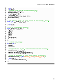
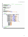
1.5.2 Actual state: Mnemosine MK III
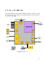
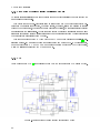
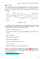
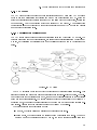
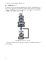
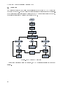
Mnemosine MK III is made up of the following nodes: Terpsicore, Urania, Melete, Polimnia,
Eutherpe and Talia.
Figure 1.1: Block diagram of Mnemosine MK III
Clio, performs data logging on Secure Digital card (SDC) using a specic CAN data logger.
Calliope, receives the signal from the Load Cell Embedded Digitiser and creates the message
to be sent on the bus.
Eutherpe, through the use of potentiometers allows the monitoring of the positions of
equilibrator, ailerons, aps and pedals.
Melete, is the power unit.
Melpomene, communicates with the command and display unit (CDU).
Polyhymnia, via GPS module, it transmits speed, position and satellites in view with a
frequency of 4 Hz on the data bus.
Talia, engine data, through a Hall eect sensor calculates the speed rotation of the propeller.
Terpsichore, communicates serially with AHRS 400CC-200 [4] with a frequency of 58 Hz
providing speed and angles of roll, pitch and yaw, as well as accelerations along the three
axes XYZ.
Urania, in eect an air date computer, uses a dierential pressure sensor MPXV5004G[5]
and a absolute pressure MPX5100[6].It allows to obtain information on: static pressure,
dynamic pressure, temperature and angles of attack and sideslip.
9
1 Introduction
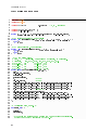
1.6 Operating limits
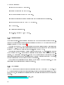
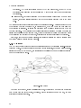
After using the system for few years, some critical aspects have been found:
rst of all the
decentralized nature in multiple nodes leads to an increase of the space occupied by the system;
data was asynchronous and aected by presence of short random data delay. As a matter of fact
it has been noted that it needs a new on-board user interface.
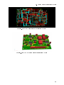
Figure 1.2: Mnemosine MK III installed on board
10
1.7 Upgrade requirements
1.7 Upgrade requirements
At rst glance it is immediately apparent the need for a deep change in the conguration, the
integrated architecture makes it possible to obtain smaller volumes and in this case it's the
highest grade of eciency. In order to face the undesired presence of asynchronism it will be
used a deterministic software, while as far as it concerns the last issue it is necessary to design
a new user interface.
Collecting all the ideas it's possible to write the new high level requirements and the new
Mnemosine MK IV will be made up by: a microcontroller unit (MCU) mounted on the mother
board which also provides: all inputs for external sensors, all power supply components and of
course all plug connectors for external module. Mnemosine MK IV will be equipped with sensors
able to acquire:
air data: total air pressure, static air pressure, angle of attack (AOA), angle of sidesleep
(AOS)
engine data: propeller revolutions per minute (RPM), fuel ow, exhaust gas temperature
(EGT)
control surface positions: aileron, equilibrator, rudder, ap
stick forces
3D inertial data: accelerations, Eulerian angle rates, Eulerian angles
GPS data
The lower level requirements of Mnemosine MK IV must ensure:
the use of a standard development board
communication with:
GPS module with time pulse over UART port
attitude heading reference system(AHRS) platform over multi-mode serial peripheral
interface (RS232, RS485, RS422)
embedded stick force acquisition system over multi-mode serial peripheral interface
(RS232, RS485, RS422)
SD card
CDU also through bluetooth module
Ethernet port
CAN port
air data computer (ADC) over Inter-Integrated Circuit port (I C)
²
possibility of software upgrade through universal asynchronous receiver-transmitter port
(UART)
11
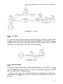
2 Hardware Realization
All the choices that led to the nal hardware conguration of the system Mnemosine MK IV will
be motivated in this chapter. Obviously it was an iterative process with the aim of nding the
best t of the requirements.
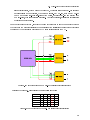
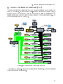
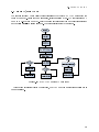
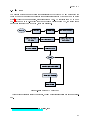
Figure 2.1: Mnemosine MK IV
13
2 Hardware Realization
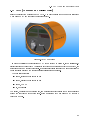
Figure 2.1 allows to observe all the hardware subsystems that compose MK IV, comparing
it with the diagram of MK III it is immediately note the absence of a data bus in favor of an
integrated architecture. The only external module is Urania (air data) that communicates with
²
the main board using I C protocol.
The entire system is enclosed in a metal case that will
protect the delicate circuits during the ight test. It should be noted the ability to update the
software externally, without changing the boarded conguration; this skill ensures a high degree
of software maintainability.
Figure 2.2: Mnemosine MK IV Rendering
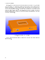
The new hardware architecture allows to assemble the most part of the system inside one
single metal case.
14
2.1 Development board
2.1 Development board
As previously mentioned Mnemosine MK IV is constituted by a single central core:
the mi-
crocontroller. Currently there are hundreds, if not thousands, of models all dierent from each
other, each one having its own features. By conducting research in the automotive and industrial
automation it has been possible to draw up a list of products. Through a simple comparison it
emerged that the more suitable microcontroller for our purposes is produced by STMicroelectronics [21] and it's called STM32F407.
2.1.1 STM32F407
STM32F407 is in fact not a single chip but identies a whole family of controllers based on
ARM CORTEX-M4 32-bit with reduced instruction set code (RISC)[23] capable of operating up
to 168 MHz (clock frequency). The CORTEX M4 is equipped with a single precision oating
point unit (FPU) and is therefore able to work with all types of data and instructions.
An-
other peculiarity is the presence of a digital signal processor (DSP) and memory protection unit
(MPU) that improves the security of the application code[13]. The memory of the microprocessor
is composed by up to 1 Mbyte of ash memory and up to 192+4 Kbytes of static random access
memory (SRAM) including 64 Kbyte of core coupled memory (CCM) that certainly guarantees
an adequate memory space for the full application of Mnemosine MK IV. The timing source
is composed by a factory-trimmed (1% accuracy) 16 MHz crystal oscillator and a 32 kHz oscillator for the real-time clock separately powered, which can rely on 4 KBytes of SRAM. The
microcontroller shall be supplied from 1.8 V to 3.6 V.
It's possible to obtain a maximum of three 12 bit, 2.4 MSPS analog to digital converters (ADC)
with up to 24 channels and 7.2 MSPS in triple interleaved mode. In opposite direction are also
being oered two 12 bit digital to analog converters (DAC). There are 16 stream direct memory
access (DMA), that can be used to direct transfer of data from or to memory to minimize the
interruptions caused by program-controlled data transfers.
The STM32F407 contains twelve 16 bit and two 32 bit timers up to 168 MHz, each with up
to 4 input capture, output compare or pulse width modulation (PWM).
²
Up to 15 communication interfaces are present, which include: three I C interfaces, 4 universal
synchronous/asynchronous receiver/transmitter (USART) and two UART (10.5 Mbit/s, ISO
7816 interface), three SPI (37.5 Mbits/s) two of which capable of muxed full-duplex inter-IC
²
sound (I S) to achieve audio class accuracy via internal audio phase-locked loop (PLL) or external
clock. Last two communication interfaces are essential for Mnemosine: the two CAN interfaces
and Secure Digital Input/Output interface (SDIO) which allows saving all ight data.
15
2 Hardware Realization
Figure 2.3: STM32E407 Layout
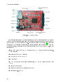
This microprocessor is used by several development board manufacturers with the eort to
meet as many as possible requirements with a single board. In this project it was decided to
use the Olimex STM32 development board-E407 equipped with STM32F407ZG[9]. This choice
is justied by the presence of connectors for devices including also the slot for SD card and
Ethernet interface, the presence of hardware abstraction layer (HAL) for ChibiOS/RT. Its main
features are:
Joint Test Action Group (JTAG) connector with ARM 2x10 pin layout for programming/debugging
Ethernet 100Mbit UEXT connector
USB host USB On The Go (OTG)
SD card Input
DC/DC power supply which allows operation from 6 V to 16 V source Power and User
LEDs
16
Reset and User buttons
4 full 20 pin Ports with the external memory bus
Dimensions: 101.6 x 86 mm
2.2 Power Supply Section
2.2 Power Supply Section
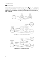
The power supply circuit must ensure an adequate stabilized voltage during all phases of ight
tests.
Especially during the critical phase of engine startup.
To meet this requirement it's
necessary to provide a separate power supply that can be replaced by the voltage coming from the
aircraft during the ight. The circuit must also ensure a minimum period of time which provides
energy to Mnemosine MK IV even if the power fails. If this happens, the board shall immediately
notify to the microcontroller in order to follow the emergency power falling procedure.
Figure 2.4: Power Supply Diagram
17
2 Hardware Realization
2.3 Multi-Mode Serial Peripheral Interface
As expressly indicated by the requirement, the system uses a number of sensors that transmit
data by serial interface directly to the doors USART or UART of the microcontroller. By the
way in the world of aviation and automation in general, there are several serial communication
protocols, including[24]:
RS232
(EIA RS-232) is a standard EIA equivalent to the European standard CCITT V21/V24.
It denes a low-speed serial interface for the data exchange between digital devices. Stretching a physical cable between two electronic devices equipped with a RS-232 port is possible
to realize a communication between them.
EIA standard RS-232 was born in the early
sixties by the work of the Electronic Industries Association and was oriented to the communication between the mainframe and terminals (Data Terminal Equipment) through the
telephone line using a modem (Data Communication Equipment). Over the years, changes
have been made to obtain dierent standards such as RS-232c widely used in the industrial
eld. Viewing from the electrical point, three logical levels are dened: mark between -3
V and -15 V, space between +3 V and +15 V and uncertainty between +3 V and -3 V.
RS-422
(EIA RS-422) is a standard EIA or CCITT V11 in European legislation. It is a protocol
for serial data communication that involves the use of two wires with multi-point dierential
line (balanced dierential).
By using two pairs of wires, and of course with two similar
circuits, it is possible to obtain the full duplex connection. Unlike EIA RS-485, from which
it diers only for the ability to be on line in the high impedance if not selected, the EIA-422
does not allow multiple transmitters but only multiple receivers. Unlike the standard EIA
RS-232 is designed to directly connect two devices (either DTE or DCE) with high noise
immunity even at considerable distances (typically up to 1550 m) and at considerable speed.
Since the change of state of the data is determined by the dierence of the voltages on the
two wires in a balanced mode (0 to +5 V and -5 V on the two conductors respectively)
and since the wire is a twisted pair this standard is resistant to the electrical noise and
jamming disturbance (high noise immunity). The maximum length of cable is 1550 m for
speeds up to 1 Mbit/s.
RS485
(EIA RS-485) equivalent to the European standard CCITT V11 is a specic OSI Model
Physical Layer of a two-wire half-duplex and multi-point serial interface.
The standard
species a management system of the signal in dierential form: the dierence between the
voltage present on the two wires constitutes the data in transit. A polarity indicates a logic
level 1 and the null state the logic level 0. The potential dierence should be at least 0.2 V
for a valid operation, but any voltage between 12 V and -7 V allows the correct operation
of the receiver. The RS-485 only species the electrical characteristics of the transmitter
and the receiver. It does not indicate or recommend any protocol for data transmission;
EIA RS-485 allows the conguration of a low cost local area networks or multi-point data
communications. It permits a very high speed transmission (35 Mbit/s up to 10 m and 100
kbps to 1.200 m). Since it uses a signaling system with a non-negligible voltage, with a
balanced line through the use of a pair of twisted cable (as is the case in the EIA RS-422),
you can reach far distances (up to 1.200 m) . Compared to the EIA RS-422, which has a
18
2.3 Multi-Mode Serial Peripheral Interface
single driver circuit, which must not be turned o, the transmitter for the EIA-485 is placed
in transmission mode explicitly, by applying a signal. EIA RS-485, such as EIA RS-422
can be made using four-wire/full-duplex (two pairs), but since EIA-485 is a specic type
of multi-point, this is not strictly necessary. As it is dierential, it resists to interferences
of electromagnetic nature.
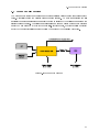
From conceptual point of view, in order to choose which standard to use to communicate between
the device and the microcontroller it becomes necessary the realization of a line driver that brings
the signal by the above listed protocols to TTL logic level useful for the MCU.
Figure 2.5: Conceptual diagram of multi-mode serial peripheral interface
Referring to Figure 2.1, it's possible to ll the following table:
mode
α
β
γ
δ
ε
o
o
o
o
o
o
232
on
o
o
o
o
422
o
on
o
o
on
485 TX
o
on
o
o
o
485 RX
o
o
on
o
o
Table 2.1: Pin conguration of multi-mode serial peripheral interface
19
2 Hardware Realization
It turns out that the Transmission Enable (δ ) of the second driver 485 will be permanently
disabled. To conclude other 4 general purpose input/output (GPIO) are needed for the following
functions:
GPIO
Function
ζ
η
ϑ
ι
+12 enable
digital out
+5 enable
event in
Table 2.2: Pin conguration of multi-mode serial peripheral interface
20
2.4 Analog Signal Conditioning Module
2.4 Analog Signal Conditioning Module
For the position detection of the control surfaces, as for the old version of the Mnemosine FTI,
potentiometric sensors will be used.
This easy integration type of sensor guarantees the per-
formance of a common linear rigid rod potentiometer but at the same time allows an adequate
safety from the moment in which a malfunction of the same, thanks to the wire behaving like
a programmed fracture, allows however the government of the surface.
The potentiometer
FMDK46-1000 produced by Atheris [25] is the smallest design in this sensor class with measuring range of 1000 mm (resolution 0.3 mm) and it is able to work within temperature range of
°
-20 C to +80
°
C.
2.4.1 Noise Filter
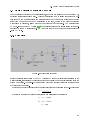
Figure 2.6: Noise Filter schematic
Before the signals are acquired by the DAC (Digital to Analog Converter) site internally in the
microcontroller, it's necessary to lter those that are obviously the more noisy signals within the
system Mnemosine. The Sallen-Key lter is used with cuto frequency less than or equal to half
of the frequency sampling.
For this type of active lter is provided an algebraic formula to calculate the cut-o frequency:
Fc =
2π
√
1
C1 C2 R1 R2
By suitably choosing the values of capacitance and resistance it is obtained:
C1 = C2 = 100
nF
R1 = R2 = 180
KΩ
Fc w 9
Hz
21
2 Hardware Realization
2.4.2 Schematics of Analog Signal Conditioning Module
To ensure electrical isolation between potentiometer and microcontroller it has been studied the
use of analog photocoupler.
This device costs of a high-brightness light emitting diode and two photodiodes tightly coupled; from the logical point of view, the input signal, a voltage, allows the passage of current
through the photoemitter, that thanks to a simple feedback circuit, emits a signal bright directly
proportional to the signal itself. At this point the second photodiode transposes the same light
signal and reconverted it into a current signal that can be reconstructed from the last operational
that actually remains isolated from the rst.
This component is produced by Avago with code HCNR20x whose performances are[27]: nonlinearity under 0.01% as ratio between the current input and output with -5% of transfer gain,
wide bandwidth from DC up to 1 MHz and worldwide safety approval (UL 1577) recognized,
minimum isolation guaranteed of 5 kV rms for 1 min.
2.4.3 PCB
Using Design Spark PCB [8] it is possible to draw both the schematics and PCB also in 3d view.
Figure 2.7: Schematics of Analog Signal Conditioning Module
22
2.4 Analog Signal Conditioning Module
Figure 2.8: PCB of Analog Signal Conditioning Module
Figure 2.9: 3D PCB of Analog Signal Conditioning Module
23
2 Hardware Realization
2.5 Secure Digital Card
This is the real physical memory of Mnemosine MK IV, that takes its name from its characteristic
to allow the protection of data stored in it. This feature is also called key revocation and allows
reading only by specic readers.
Specially developed to store information very quickly, it is
currently the digital memory of smallest size. The main characteristics of a typical
µSD
on the
market are:
Dimension: 15 mm x 11 mm x 1 mm
Default mode: 0-25 MHz, up to 12.5 MB/s interface speed
High-speed mode:0-50 MHz, up to 25 MB/s interface speed
°
°
Temperature range -25 C a +85 C
Free fall 1.5 m
MTBF > 1'000'000 h
Voltage supply 2.7 V a 3.6 V
Standby current 0.3 mA
Read/Write current 15 mA
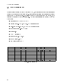
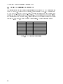
Pad Number
Name
Type
Description
Name
Type
1
DAT2
I/O/PP
data line bit2
-
-
2
CD/DAT3
3
CMD
I/O/PP
data line bit3
CS
I
chip select
PP
command/response
DI
I
data input
4
5
VDD
S
supply voltage
VDD
S
supply voltage
CLK
I
clock
SCLK
I
clock
SDIO mode
SPI mode
-
6
VSS
S
supply voltage ground
VSS
S
supply voltage ground
7
DAT0
I/O/PP
data line bit0
DO
0
data output
8
DAT1
I/O/PP
data line bit1
-
-
-
Table 2.3: pad assignment
24
Description
2.5 Secure Digital Card
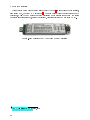
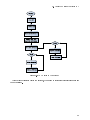
2.5.1 SPI vs SDIO
This memory supports two types of communication bus called SPI and SDIO. The rst, which
stands for Serial Peripheral Interface, is a full-duplex synchronous serial.
It is dened to use
only 4 wires and is now widely used in communication between microprocessors and sensors of
all types. The data transmission on the SPI bus is based on the operation of the shift registers.
Each device, master and slave, is equipped with an internal shift register, whose bits are output
and, simultaneously, enter via the output SDO/MOSI and the input SDI/MISO. The shift register
(8 bits) is a complete interface through which commands are given and transmitted as a serial
stream even if they are taken internally in parallel.
At each clock pulse, the devices that are
communicating on the bus lines send a bit from their internal register, replacing it with a bit
received.
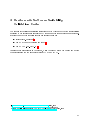
The second, Secure Digital Input/Output is an advanced standard for this type of memories
which uses several communication lines in order to improve the speed of reading or writing
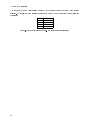
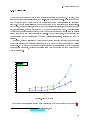
procedures. In an attempt to evaluate whether increased complications in the communication
protocol were acceptable, dierent comparison tests were made using the same hardware and
high level software.
160
SDIO
SPI
140
Tim e [ m s]
120
100
80
60
40
20
2
10
3
4
10
10
5
10
Byt e
Figure 2.10: SPI vs SDIO
As expected communication through SDIO interface is much more ecient than the SPI
1
1
.
Graph obtained using Scilab http://www.scilab.org April 4, 2013
25
2 Hardware Realization
2.6 Air Data Computer
It is the only external module of system Mnemosine MK IV, indeed to avoid a long linkage pipe
for the weak pressures detected by taps. It was decided to maintain it as unique external module
in order to facilitate as much as possible the phase of integration on the aircraft.
²
It uses the
same Urania sensors (Mnemosine MK III) and communicates via I C with the main board.
As dierential pressure transducer to measure the dynamic pressure it is used the HCLA0050EU[5]
made by Sensor Technics. Its main features are:
Range 0 to 50 hPa
Max pressure 1200 hPa
Temperature range
Sensitivity 80 mV/hPa
= °
25 C to +80
°
C
As total pressure transducer to measure the total pressure it is used the HCA0611ARH8
[6] also made by Sensor Technics. Its main features are:
Range 600 to 1100 hPa
Max pressure 3000 hPa
Temperature range 0 C to +85 C
Sensitivity 8 mV / hPa
Accuracy 1.0 % ES
Response time 2 ms
°
°
Regarding the sensors for angle of attack and sideslip, given the diculty of installation of a nose
boom in ULM aircraft, sometimes they were omitted. However the use of classical ag sensors
is always possible.
Figure 2.11: HCLA Pressure Sensors Family
26
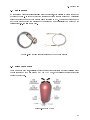
2.7 Engine Data
2.7 Engine Data
By exploiting a hall eect sensor installed near the propeller, it is possible to detect the number
of turns of the same. In order to detect the fuel consumption a fuel ow sensor may be installed
inner the engine cowl and a thermocouple allows detection of EGT. This thermocouple must be
of type J given the high temperature of the engine and must necessarily be mounted at the
critical point i.e. the less cooled part.
Figure 2.12: Typical Hall eect sensor and type J thermocouple
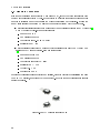
2.8 Stick Force Data
Using a small 3D load cell, originally built for automotive application and its acquisition board
that is connected with Mnemosine MK IV via UART port, it is possible to record stick force
during the ight test.
Figure 2.13: Futek MU300
27
2 Hardware Realization
This subsystem is composed of a load cell produced by Futek
3
also called DSC, produced by Mantracourt .
2
and load cell embedded digitiser,
The load cell gathers the stick forces in both
directions, while the DSC allows complete processing of the signals coming from the strain
gauges; it also transmits data, already engineered, via serial protocol to Mnemosine MK IV.
Figure 2.14: Mantracourt DSC Load Cell Embedded Digitiser
2
3
http://www.futek.com/ April 4, 2013
http://www.mantracourt.com/ April 4, 2013
28
2.9 Inertial Data
2.9 Inertial Data
To capture the inertial ight data, it is necessary to use an AHRS. It was choosed the MTi
Xsens[31].
The MTi is a miniature, gyro-enhanced Attitude and Heading Reference System.
Its internal low-power signal processor provides drift-free 3D orientation as well as calibrated
3D acceleration, 3D rate of turn and 3D earth-magnetic eld data.
The MTi is an excellent
measurement unit (IMU) for stabilization and control of cameras, robots, vehicles and other
(un)manned equipment. The main features of MTI are:
º
Real-time computed attitude, heading and inertial dynamic data 360
orientation refer-
enced by gravity and Earth Magnetic.
Field Integrated 3D gyroscopes, accelerometers and magnetometers.
On board DSP, running sensor fusion algorithm.
Gyroscopes enable high-frequency orientation tracking High update rate (120 Hz), inertial
data processing at max 512 Hz.
Individually calibrated for temperature, 3D misalignment and sensor cross-sensitivity.
Accepts and generates synchronization pulses.
This last point is prime for Mnemosine MK IV that is a synchronous real time system and allows
the essential command response from the board and the MTi. The MTi returns and technical
specications are:
·
·
·
·
·
°
3D Orientation (360 )
3D rate of turn
Static accuracy (roll / pitch) <0.5
°
Dynamic accuracy 2 RMS
Operating voltage 4.5 - 30 V
·
·
° ·
·
·
3D acceleration
3D magnetic eld
Digital interface RS-232, RS-485, RS-422
°
Static accuracy (heading) <1
Angular resolution 0.05
°
Figure 2.15: Xsens MTi
29
2 Hardware Realization
2.10 GPS Data
The GPS module for Mnemosine MK IV is not just a simple position sensor but it is the main
source of the entire time system, this means that it is probably one of the major critical points
of the whole project.
As previously mentioned, Mnemosine MK IV allows to acquire measurements synchronously;
to obtain this, the system receives in input a pulse every second that gives start to a default
sequence of operations. Thus the source of time is the external time-pulse of GPS. Following a
brief marketing research the LEA-5T made by U-Blox [32] has been chosen as Mnemosine GPS
module.
The LEA-5T features a Time Mode function whereby the GPS receiver assumes a stationary
3D position, either manually programmed or determined by an initial self-survey.
Stationary
operation enables GPS timing with only one visible satellite and eliminates timing errors which
otherwise would result in positioning errors. The accuracy of the time pulse is as good as 30 ns,
synchronized to GPS or UTC time. An accuracy of 15 ns is achievable by using the quantization
error information to compensate the granularity of the time pulse.
A built-in time mark and
counter unit provides precise time measurement of an external signal (EXTINT0 input). Main
features:
50-channel U-Blox 5 engine with over 1 million eective correlators.
Hybrid GPS, GALILEO and Satellite-Based Augmentation System (SBAS) engines like
WAAS, EGNOS, MSAS, GAGAN.
< 1 second Time-To-First-Fix for hot and aided starts.
Stationary mode for GPS timing operation.
Super sense indoor GPS with best-in-class acquisition and tracking sensitivity.
Output time pulse with at least one satellite in view.
Figure 2.16: U-Blox LEA-XT
30
2.11 CDU (Command and Display Unit)
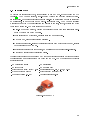
2.11 CDU (Command and Display Unit)
Inside the aircraft the operator has two CDUs. The rst controls the power supply circuits of
Mnemosine MK IV and contains the recording switch.
Figure 2.17: CDU Rendering
In order to facilitate the integration of CDU it was decided to design it, into a classical 3.5
aircraft instrument case; this CDU is splitted into three main parts: the rotary power switch, the
recording switch and the light indicators. Its minimalist design ensures the minor probability to
cause confusion although the operator retains full situation awareness.
The four lights identify:
Orange, external power supply in use
Green 1, aircraft power supply in use
Green 2, GPS x
Red, Recording!
The second, currently under development, is a multifunction touchscreen that makes possible to
upload the test card or other documents. It communicates with Mnemosine MK IV through a
bluetooth module.
31
3 Software Realization
Once dened the physical structure of the system, it is now possible focus on the software. In
this chapter all the choices that have been carried out for the operating system and application
software will be introduced and motivated.
3.1 Real Time Operating System
From rst instant it was clear that in order to meet the requirements, the presence of a realtime operating system had to be considered imperative. Mnemosine MK IV, like other real-time
systems are characterized by the severe consequences that result if logical as well as timing
correctness properties of the system are not met.
and hard.
Two types of real-time systems exist: soft
In a soft real-time system, task are performed by the system as fast as possible,
but the task don't have to nish by specic times. In hard real-time systems, task have to be
performed not only correctly but on time. Mnemosine MK IV like most real-time systems have
a combination of soft and hard requirements.
This systems are called foreground/background
systems or super-loops.
An application consists of an innite loop that calls modules (i.e., function) to perform the desired operation (background or task level ). Interrupt service routine (ISR) handles asynchronous
events (foreground) that is also called interrupt level.
Critical operations must be performed by ISRs to ensure that they are dealt with in timely
fashion. Because of this, ISRs have the tendency to take longer than they should. Also, information for background module that an ISR makes available is not processed until the background
routine gets its turn to execute, which is called the task-level response.
During the operation of the software, the Real Time Operating System (RTOS) inside Mnemosine MK IV must guarantee the determinism of events, for this reason all task and functions have
a specic timeout.
Shared Resource:
can be used by more than one task.
Each task should gain exclusive
access to shared resource to prevent data corruption. This process is called mutual exclusion and
of course this feature must be present in the chosen RTOS.
Multitasking:
is the process of scheduling and switching the central processing unit (CPU)
between several tasks; Multitasking allow to have more backgrounds, this helps to design a
specic application for each peripheral of the system, these application program are easier to
design and to maintain in comparison to a single background software.
Currently there are many types of operating systems, each of them with their own particularities and peculiarities. Below it will be exposed the motivations that led to the choice of the
RTOS.
33
3 Software Realization
Task:
also called thread, is a simple program that thinks it has the CPU all to itself. The
design process for our real-time application involves splitting the work to be done into tasks
responsible for a portion of the problem. To each task is assigned a priority, its own set of CPU
registers, and its own stack area.
Kernel:
is the part of multitasking system responsible for management of task i.e., for man-
aging the CPU's time and communication between tasks. A kernel adds overhead to the system
because the services provided by the kernel requires execution time. The amount of overhead
depends on how often these services are invoked and naturally how the kernel is made. One of
the major performance index for kernel is the
Context Switch.
When a multitasking kernel
decides to run a dierent task, it saves the current task's context (CPU registers) in the current
task's context storage area. After this operation is performed, the new task's context is restored
from its storage area and then resumes execution of the new task's code.
Preemptive kernel means that the highest priority task ready to run is always given control
of CPU. It is used when system responsiveness is important, therefore this feature is explicitly
required. When a task makes a higher priority task ready to run, the current task is preempted
(suspended), and higher priority task is immediately given control of the CPU. If an ISR makes
a higher priority task ready, when the ISR completes, the interrupted task is suspended, and the
new higher priority task is resumed[35].
3.1.1 Choosing the RTOS
Using a survey in the RTOS world and excluding all operating systems with proprietary license,
substantially two products are emerged : FreeRTOS [10] and ChibiOS/RT [11]. Remembering
that both FreeRTOS and ChibiOS/RT are distributed under GPL3 license [12], this means that
it can be used the code or part of code for a commercial product.
The reasons that led to
the choice of ChibiOS compared to FreeRTOS can be summarized as: ChibiOS/RT is designed
for deeply embedded real time applications where execution eciency and compact code are
important requirements. This RTOS is characterized by its high portability, compact size and,
mainly, by its architecture optimized for extremely ecient context switching.
ChibiOS/RT
has an ecient and portable preemptive kernel, best in class context switch performance i.e.,
withARMCM3/STM32F4xx-168-GCC4.6.2 the context switch time is 0.40µS with a kernel size
of 6172 byte (all the non-debug subsystems enabled). The architecture is static, everything is
statically allocated at compile time nevertheless dynamic extensions and objects are supported by
an optional layer built on top of the static core. There is an entire set of primitives: threads, virtual timers, semaphores, mutexes, condition variables, messages, mailboxes, event ags, queues.
It support priority inheritance algorithm on mutexes. HAL component supporting a many if not
all abstract device drivers also supporting external components like uIP, lwIP and FatFs essential
for the proper functioning of the SD card.
34
3.1 Real Time Operating System
The ChibiOS's father is Giovanni Di Sirio, in the eighties he developed an ancestor that was
an Operating System for Motorola 68000 [17].
In 1989 it supported GCC, ran EMACS, was
preemptive and real-time but in 1991 Linus Torvalds began the development of Linux and the
project changed course. The original full-featured OS turned in a minimalistic, ecient, RTOS:
ChibiOS/RT's father... In 2007, 15 years later, it turned to ChibiOS/RT: an open source RTOS
project targeted to embedded systems.
Currently the project is led and mainly developed by
Giovanni Di Sirio and in the last years ChibiOS/RT started growing in features, ports and users...
Now it is a real software community.
As underlined ChibiOS/RT is meant to be a whole operating system not just a scheduler. The
kernel has no internal tables, there is nothing that must be congured at compile time or that
can overow at run time, no upper bounds, the internal structures are all dynamic even if all
the objects are statically allocated.
System application program interface (API) has no error
conditions, all the previous points are nalized to this objective. The APIs are not slowed down
by parameter checks; they do exist but only are activated when the related debug switches. All
the static core APIs always succeed if correct parameters are passed. Exception to this rule are
the optional dynamic APIs that, of course, can report memory exhausted.
Note, rst fast then compact, the focus is on speed and execution eciency and then on
code size. This does not mean that the OS is large, the kernel size with all the subsystems
activated weighs around 5.5KiB (STM32, Cortex-M3).
Test results on all the supported platforms and performance metrics are included in each ChibiOS/RT
release. The test code is released as well, all the included demos are capable of executing the
test suite and the OS benchmarks[30].
35
3 Software Realization
3.2 Development Environment
The development environment chosen for the realization of the software is ChibiStudio. It is an
Integrated Development Environment (IDE) composed by freely distributed softwares grouped
in a handy suite.
It is essentially composed by Eclipse Juno 4.2 classic, congured for execution of embedded
applications.
Today is ocially distributed and free of charge
1
for Windows platform and unocially for
2
Linux .
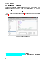
Figure 3.1: ChibiStudio screen shot
See Appendix C for the complete ChibiStudio software components.
1
2
http://sourceforge.net/projects/chibios/les/ChibiStudio/ 4 April, 2013
ftp://ftp.elet.polimi.it/users/Martino.Migliavacca/ 4 April, 2013 - Special thanks to Ing. Martino Migliavacca
Dipartimento di Elettronica E Informazione del Politecnico di Milano
36
3.3 Thread denitions (High Level Software Requirements)
3.3 Thread denitions (High Level Software Requirements)
The software is mainly divided into threads, each thread manages its own work. The purpose of
the threads is to support the following capabilities:
Data acquisition of the following parameters:
Air data: static pressure P_STAT, dynamic pressure P_DIN, OAT, AOA, AOS.
GPS data: 3D ECEF position, 3D ECEF velocity.
Stick force.
Control Surface positions: elevator ELE_POS, rudder RUD_POS, aileron AIL_POS,
aps FLP_POS.
²
Engine data: RPM, EGT, Fuel Flow. Data saving on secure digital SD.
ETH port communication.
CAN port communication.
I C port communication.
Software maintenance via UART port.
Ensure data synchronization
The following notation has been used in order to guarantee a project-unique identier for each
operational software (OPSW) requirement:
THD_xxx_yyy_zzz
The characters xxx denote the type the requirement belongs to, among the following:
HAL
COM
CAL
SAV
UPT
EXP
hardware abstraction layer
peripheral communication
calculate/compute/do something
save
update
export data
The characters yyy denote the type the requirement belongs to, among the following:
DEF
STP
FUN
denition
setup structure
function
and zzz denote a serial number useful for identication.
As mentioned ChibiOS / RT is written entirely in ANSI C, for this reason all the code that
will be proposed is intended written in this language; hereinafter will displays all the expected
threads with their general characteristics.
37
3 Software Realization
3.3.1 Main
The main has the task to initialize the operating system according to the operating parameters
of the board OLIMEX STM32E407 [9], allow the creation of all threads and their respective mail
boxes. Substantially the work of the script main ends with the initialization phase, where the
thread scheduler thanks to the operating system takes control of the entire software, common
aspect of all embedded real time operating systems.
3.3.2 Time scheduler
The time scheduler is not just a simple thread but a set functions independently managed through
the use of hardware and software interrupts.
It receives a pulse every second from GPS time
pulse, starting from here and knowing the sampling frequencies of all desired measures, a timer
starts and sends a startup message that allows the execution of the task. To give a fair priority
execution to each thread it is set at the creation time in the main. The priority policy is based on
the need of time of each task. Assigning task priorities is not a trivial undertaking because of the
complex nature of real-time system. An interesting technique called rate monotonic scheduling
(RMS) has been established to assign task priorities based on how often tasks execute. Simply
put, tasks with the highest rate of execution are given the highest priority.
Given a set of n task that are assigned RMS priorities, the basic RMS theorem states that
all task hard real-time deadlines are always met if the inequality in the following equation is
veried.
P Ei
≤ n 21/n − 1
i
Ti
Where
Ei
corresponds to the maximum execution time of task i and
execution period of task i. In other words,
Ei
Ti
Ti
corresponds to the
corresponds to the fraction of CPU time required to
execute task i [35]. It is likely that Mnemosine MK IV can not be run entirely by this philosophy,
but RMS is a good starting point.
38
3.3 Thread denitions (High Level Software Requirements)
3.3.3 SD thread
The SD thread should congure hardware abstraction layer and ChibiOS's SDC module. The
SDC driver implements a state machine internally, not all the driver functionalities can be used
in any moment, any transition not explicitly shown in the following diagram has to be considered
an error...
Figure 3.2: SDC diagram
In agreement with the above diagram, the thread must initialize the driver from left to right.
After the initialization phase, the thread enters a phase of waiting until it is released by the time
scheduler. The software should guarantee the following functions:
create a new mission folder in the SD card
create e close a new le each second where writes all acquired measurements in that time
period
start/stop recording
communicates its state and errors
keeping track of all written bytes
keeping track of all free bytes in the SD card
mount/unmount card
secure power falling procedure without loss of information
3
In order to use SD card a le system is needed, ChibiOS uses FatFS . FatFs is a generic FAT
le system module for small embedded systems. The FatFs is written in compliance with ANSI
C and completely separated from the disk I/O layer. Therefore it is independent of hardware
architecture, its features are:
3
http://elm-chan.org/fsw//00index_e.html April 4, 2013
39
3 Software Realization
Windows compatible FAT le system.
Platform independent and easy to port.
Very small footprint for code and work area.
Various conguration options: Multiple volumes (physical drives and partitions).
Long le name support in ANSI/OEM or Unicode.
RTOS support.
Multiple sector size support.
Read-only, minimized API, I/O buer.
3.3.4 Ethernet thread
This thread uses light-weight Internet Protocol (lwIP) that is a small independent implementation of the transmission control protocol for Internet Protocol (TCP/IP) suite that has been
4
initially developed by Adam Dunkels .
The focus of the lwIP TCP/IP implementation is to reduce resource usage while still having
a full scale TCP. This makes lwIP suitable for use in embedded systems with tens of kilobytes
of free RAM and around 40 kilobytes of code read-only memory (ROM).
Main features include: Internet Control Message Protocol (ICMP), Point-to-Point Protocol
Over Ethernet (PPPoE). Other extended features:
IP forwarding over multiple network in-
terfaces, TCP congestion control, round-trip time (RTT) estimation and fast recovery/fast retransmit; are also includes addon applications like Hypertext Transfer Protocol (HTTP) server,
Network Basic Input/Output System (NetBIOS) nameserver.
The Ethernet port will ensure proper delivery of data stream to ground stations. The data
transmission is unidirectional from airplane to ground.
3.3.5 CAN thread
The CAN thread should congure hardware abstraction layer and ChibiOS's CAN module. The
CAN driver implements a state machine internally, not all the driver functionalities can be used
in any moment, any transition not explicitly shown in the following diagram has to be considered
an error.
4
http://savannah.nongnu.org/projects/lwip/ April 4, 2013
40
3.3 Thread denitions (High Level Software Requirements)
Figure 3.3: CAN diagram
3.3.6 GPS thread
The GPS thread should congure hardware abstraction layer and ChibiOS's SD (Serial Driver)
module. The thread is generally divided into 2 parts, the initialization should perform a communication test that checks the GPS operation; while the innite loop is freed from time scheduler
every 200 ms (5 Hz), it requires GPS data and check its integrity.
Figure 3.4: SD driver
3.3.7 Stick force thread
The stick force thread should congure hardware abstraction layer and ChibiOS's UART module.
After the initialization phase, the thread must perform a communication test, in case of errors
will have to report it in an appropriate way.
Every 100 ms (10 Hz), the time scheduler will ensure the enforceability of the loop using
the traditional command-response method with the stick force conversion board sited near the
cloche.
41
3 Software Realization
3.3.8 AHRS thread
It is the thread that runs at higher frequency (50 Hz or 20 ms).
The AHRS thread should
congure hardware abstraction layer and ChibiOS's UART module.
After the initialization
phase, the thread must perform a communication test, in case of errors must report it in an
appropriate way. Once entered the stage of loop, it should require the latest data to the AHRS,
receive and store it.
Figure 3.5: UART driver
Figure 3.6: UART driver transmission diagram
Figure 3.7: UART driver receiver diagram
42
3.3 Thread denitions (High Level Software Requirements)
3.3.9 CDU thread
The CDU thread should congure hardware abstraction layer and ChibiOS's UART module in
order to use the multifunction touchscreen and other GPIO peripheral for the CDU. Since the
rotary supply selector switch is fully connected to Mnemosine with hardware cables, no software
code is needed.
Only the recording switch is monitored by the thread.
The multifunction
touchscreen is linked with bluetooth module that is actually a normal UART module and doesn't
need a specic abstraction layer.
3.3.10 Control surface position thread
The CDU thread should congure hardware abstraction layer and ChibiOS's ADC module. The
driver implements a state machine internally, not all the driver functionalities can be used in any
moment, any transition not explicitly shown in the following diagram has to be considered an
error.
Figure 3.8: ADC driver
The ADC Conversion Group is the object that species a physical conversion operation. This
structure contains some standard elds and several implementation-dependent elds. The standard elds dene the conversion group mode, the number of channels belonging to the conversion
group and the optional callbacks. The implementation dependent elds specify the physical ADC
operation mode, the analog channels belonging to the group and any other implementation specic setting. Usually the extra elds just mirror the physical ADC registers.
The driver supports three conversion modes:
One Shot, the driver performs a single group conversion then stops.
Linear Buer, the driver performs a series of group conversions then stops.
This mode
is like a one shot conversion repeated N times, the buer pointer increases after each
43
3 Software Realization
conversion.
The buer is organized as an S(CG)*N samples matrix, when S(CG) is the
conversion group size (number of channels) and N is the buer depth (number of repeated
conversions).
Circular Buer, much like the linear mode but the operation does not stop when the buer
is lled, it is automatically restarted with the buer pointer wrapping back to the buer
base.
The driver is able to invoke callbacks during the conversion process. A callback is invoked when
the operation has been completed or, in circular mode, when the buer has been lled and
the operation is restarted.
In linear and circular modes a callback is also invoked when the
buer is half lled. The half lled and lled callbacks in circular mode allow to implement
streaming processing of the sampled data, while the driver is busy lling one half of the buer
the application can process the other half, this allows for continuous interleaved operations.
Said this, more than one choice is possible, it is currently foreseen the use of a circular buer
to obtain a ltered measure for each channel.
3.3.11 Air thread
²
The AIR thread should congure hardware abstraction layer and ChibiOS's I C (Inter-Integrated
Circuit) module. The driver implements a state machine internally, not all the driver functionalities can be used in any moment, any transition not explicitly shown in the following diagram
has to be considered an error.
²
Figure 3.9: I C driver
As for the other thread, after an initialization phase, the algorithm must test communication
with the air data computer Urania, if positive, with an interval of 100 ms (10 Hz), the time
scheduler require its execution.
44
3.4 Software Requirements Specication (SRS)
3.4 Software Requirements Specication (SRS)
A Software Requirements Specication (SRS) is a complete description of the behavior of a
system to be developed. In order to align a well-established practice in the aviation world, it
is decided to draw up a formal SRS document that permits to verify the satisfaction of the
requirements set forth above and allows to write a faster and more ecient source code. The
document is entirely given in Appendix A.
Figure 3.10: Overall Software Conguration Flowchart
The diagram in Figure 3.10 shows the complete software architecture, which summarizes all
the individual threads previously seen.
45
4 Hardware & Software Suitability
Validation Code
The purpose of the following suitability validation code (SVC) is to show that the characteristics
expressed by the requirements are fully met by the union of the chosen hardware and software.
It should be noted that the following demos require the use of:
ChibiStudio v2.5 or later
1
OLIMEX STM32E407 development board
OLIMEX ARM-USB-TINY-H
2
3
All source code are presented in Appendix B, while Appendix C shows how to load and update
the software using the two supported systems (UART and JTAG).
1
2
3
http://sourceforge.net/projects/chibios/les/ChibiStudio/ April 4, 2013
https://www.olimex.com/Products/ARM/ST/STM32-E407/ April 4, 2013
https://www.olimex.com/Products/ARM/JTAG/ARM-USB-TINY-H/ April 4, 2013
47
4 Hardware & Software Suitability Validation Code
4.1 Serial Driver SVC
The purpose of this SVC is to verify the functionality of the ChibiOS/RT Serial Driver with the
board STM32E407. While the code is running, the green led blinks every second and connecting
a USB-TTL converter from PC to PD11 (TX-data) and PD12 (RX-data) with a serial virtual
terminal, the hello world!!! message is shown.
Figure 4.1: Serial Driver SVC Flowchart
After having extensively tested the software, the serial port communication requirement is
deemed satised.
48
4.2 USART/UART SVC
4.2 USART/UART SVC
The purpose of this SVC is to verify the functionality of the ChibiOS/RT UART Driver with the
board STM32E407. While the demo is running, after connecting a USB-TTL converter from PC
to PD11 (TX-data) and PD12 (RX-data) the green led blinks every time a character is received
or the hello world!!! message is shown. The driver restarts every ve seconds.
Figure 4.2: USART/UART Driver SVC Flowchart
After having extensively tested the software, the UART port communication requirement is
deemed satised.
49
4 Hardware & Software Suitability Validation Code
4.3 Analog to Digital Converter SVC
The purpose of this demo is to verify the functionality of the ChibiOS/RT ADC Driver with the
board STM32E407.
While the demo is running, after connecting a USB-TTL converter from
PC to PD11 (TX-data) and PD12 (RX-data), the green led blinks every time a string, that
contains the eight measure repeated twice, is shown.
and continuously every 56 system ticks.
The conversions are done automatically
Please note that the conversion is valid for a signal
between 0V - 3.3V and 3.3V is the maximum voltage rating. The eight values come from:
ADC3 Channel
STM32 Pad
External Connector Pin
IN9
PF3
PF pin 6
IN14
PF4
PF pin 7
IN15
PF5
PF pin 8
IN4
PF6
PF pin 9
IN5
PF7
PF pin 10
IN6
PF8
PF pin 11
IN7
PF9
PF pin 12
IN8
PF10
PF pin 13
Table 4.1: ADC board: pin conguration
50
4.3 Analog to Digital Converter SVC
Figure 4.3: ADC Driver SVC Flowchart
After having extensively tested the software, the analog to digital converter requirements are
deemed satised .
51
4 Hardware & Software Suitability Validation Code
4.4 SD SDIO Mode SVC
The purpose of this demo is to verify the functionality of the ChibiOS/RT SDIO Driver with
the board STM32E407. While the demo is running, after connecting a USB-TTL converter from
PC to PD11 (TX-data) and PD12 (RX-data) the green led blinks every half second. If WakeUP
button is pushed the SDIO's test is performed. The task reads information about the SD card
inserted and displays the results on the serial terminal emulator; a new mission folder is created
and inside the directory is written a generic log00.dat le.
Figure 4.4: SDIO Driver SVC Flowchart
After having extensively tested the software, the SDIO operational requirements are deemed
satised.
52
4.5 Time Scheduler SVC
4.5 Time Scheduler SVC
The purpose of this demo is to verify the functionality of the ChibiOS/RT EXT and GPT Drivers
with the board STM32E407 in order to simulate the Time Scheduler thread. While the demo is
running, after connecting a USB-TTL converter from PC to PD11 (TX-data) and PD12 (RXdata), the Time Scheduler test is performed if WakeUP button is pushed. All timer interrupts
are hardware interrupts so the CPU is free to execute threads instructions during the message
post. All the threads do nothing but write their own identier character in the output structure
shown on the terminal at the end of execution.
Figure 4.5: Time Scheduler SVC Flowchart
53
4 Hardware & Software Suitability Validation Code
1
Serial : ( / dev / ttyUSB0
,
38400 ,
8,
1,
None , None − CONNECTED )
2
3
4
5
6
7
8
9
AHRS
CSP
AIR
SF
GPS
CDU
SD
THREAD !
THREAD !
THREAD !
THREAD !
THREAD !
THREAD !
THREAD !
AHRS
CSP
AIR
SF
GPS
CDU
A_A_A_A_A_A_A_A_A_A_A_A_A_A_A_A_A_A_A_A_A_A_A_A_A_A_A_A_A_A_A_A_A_A_A_A_A_A_A_A_A
C____C____C____C____C____C____C____C____C____C____C____C____C____C____C____C____C
R_________R_________R_________R_________R_________R_________R_________R_________R
S_________S_________S_________S_________S_________S_________S_________S_________S
G___________________G___________________G___________________G___________________G
U________________________U________________________U________________________U_____
10
11
12
13
14
15
16
As it's visible from the results, ChibiOS proves to be able to fully meet the time scheduling
requirements.
54
4.6 Input Capture SVC
4.6 Input Capture SVC
The purpose of this demo is to verify the functionality of the ChibiOS/RT ICU Driver with the
board STM32E407 in order to simulate the capture of enigine's RPM. While the demo is running,
after connecting a USB-TTL converter from PC to PD11 (TX-data) and applying a square wave
to PD pin 16, the thread every 200 ms shows on the terminal the period of wave and in case of
timer overow it displays overow=1. It should be noted once again that all timer interrupts
are hardware interrupts so the CPU is completely free.
Figure 4.6: Input Capture SVC Flowchart
After having extensively tested the software, the ICU operational requirements are deemed
satised.
55
4 Hardware & Software Suitability Validation Code
4.7 CAN SVC
The purpose of this demo is to verify the functionality of the ChibiOS/RT CAN Driver with
the board STM32E407. The demo uses two dierent threads: the transmitter and the receiver.
Every half a second transmitter sends a message on the CAN bus (congured in loopback mode),
the message is transposed by receiver that ashes the LED.
Figure 4.7: CAN Driver SVC Flowchart
After having extensively tested the software, the CAN operational requirement is deemed
satised.
56
4.8 I²C SVC
4.8 I²C SVC
²
The purpose of this demo is to verify the functionality of the ChibiOS/RT I C Driver with the
board STM32E407 in order to acquire the three angle rates provided by IDG600 (3D mems rate
4
gyro) . While the demo is running, after connecting a USB-TTL converter from PC to PD11
(TX-data) and PD12 (RX-data) and the gyro to the I2C2 driver (PFpin3 & 4), the thread shows
on the terminal every 50 ms the yaw, pitch and roll rates.
²
Figure 4.8: I C Driver SVC Flowchart
²
After having extensively tested the software, the I C operational requirement is deemed satised.
4
http://invensense.com/mems/gyro/itg3200.html April 4, 2013
57
5 Conclusion and Future Developments
5.1 Prototyping
Now that the hardware and software conguration until the test demos has been fully described,
it's time to create the rst prototype.
First, it is necessary to integrate the wiring diagrams to realize the motherboard which will
be assembled on the microcontroller and other peripheral cards including GPS module.
Considering a work team consisting of one person and a project manager, it is expected that
the hardware integration phase, including also the physical realization of the board, should last
about two months.
The second step is to write the denitive source code which can be then tested in its entirety,
and decide the size of the individual threads i.e.
the physical division of the RAM that at
this design stage couldn't be determined. At the beginning, the task priority will be assigned
according to the rate monotonic scheduling philosophy, where basically high speed thread has
priority on low speed thread.
After having extensively tested the software and according to
their results, it will be obviously clear the good task priority policy. Considering a work team
consisting of one person and a project manager, it is expected that the software integration
phase, including the debugging of the source codes, should last about two more months.
The third phase will involve the nal integration of the system initially within ight case and
then on board of an ULM; the occasion could probably occur during the ight tests performed
during the course of Sperimentazione in Volo which is discussed in advance. Considering a work
team consisting of one person, a project manager and one aircraft's specialist, it is expected that
the nal integration phase, until the rst ight test, should last about three more weeks. However,
considering strong innovation in the project, it is reasonable to expect at least a week of delay
for each phase.
5.2 Conclusion
The aim of the present work was to verify the feasibility of the project coming to the preliminary
design of both hardware and software of the new data acquisition system for ight test of ULM.
The work started from requirements analysis, while to choose the sensors performance and
their measurement range it has been taken for granted the past experience (Mnemosine MK III).
In accordance with the mission requirements, the sensors that are currently been identied as the best possible choice are: Olimex STM32E407 development board, Sensors Technics
HCLA0050EU and HCA0611ARH8 pressure sensors, Xsens MTi AHRS, U-Blox LEA-5T GPS
module.
59
5 Conclusion and Future Developments
In the last days before the end of the thesis, two other requirements have been added. Today
it is increasingly common to use EFIS (Electronic Flight Instrument System) specialized for
light aircraft and it is requested the ability to interface this device with Mnemosine. The second
request is the ability to record cockpit voice directly with MK IV to get a synchronous audio
track with other aircraft data.
The choice of how to arrange the boards inside the hardware case has not been decided yet.
Preserving the schematics more than one conguration is possible and during the prototyping
phase will be identied the best choice. The most suitable solution now consists of a horizontal
motherboard where the MCU is also housed horizontally, while the serial adapter boards and
the analog conditioning boards are arranged vertically hence connected by side. It is expected
that this arrangement minimizes the volume used.
Figure 5.1: Boards Arrangement
Using all Open Source SW helped to keep down the overall budget. It was possible to test all
the features of the system by purchasing only the development board and the debugger for about
a hundred euros. Currently it is expected a nal expenditure in line with the budget estimated
in the preliminary phase for about a few thousand euros.
The strong push by the authorities for a safer aviation, will force the aviation industry to
perform more systematic ight test campaign and we are condent that Mnemosine MK IV
will be the reference point for the Design and Development of each Flight Test Instrumentation
System for Light Aircraft.
60
Bibliography
[1]
MNEMOSINE: A FEDERATED FLIGHT TEST INSTRUMENTATION SYSTEM FOR
SPORT AVIATION AIRCRAFT, C. Cardani, A. Folchini, A. Rolando 19th AIDAA National Congress, Forlì, Italy, September 17-20, 2007
[2]
R. B. GmbH, CAN Specication - Version 2.b
[3]
M. S. F. Systems, CANAerospace. Interface specication for airborne CAN applications - V
1.7
[4]
C. Technologies, AHRS400 Series User's Manual.
[5]
F. Semiconductor, MPXV5004G SERIES Integrated Silicon Pressure Sensor On-Chip Signal
Conditioned, Temperature Compensated, and Calibrated - Technical data, 2007.
[6]
F. Semiconductor, MPX5100/MPXV5100 SERIES Integrated Silicon Pressure Sensor OnChip Signal Conditioned, Temperature Compensated, and Calibrated - Technical data, 2005
[7]
http://www.aero.polimi.it
April 4, 2013
[8]
http://www.designspark.com/ April 4, 2013
[9]
Olimex ltd, STM32-E407 development board - User Manual
[10] http://www.freertos.org April 4, 2013
[11] http://www.chibios.org/dokuwiki/doku.php April 4, 2013
[12] http://gplv3.fsf.org/ April 4, 2013
[13] STMicroelectronics, STM32F407xx Reference Manual
[14] http://dunkels.com/adam/ April 4, 2013
[15] http://savannah.nongnu.org/projects/lwip/ April 4, 2013
[16] http://elm-chan.org/fsw//00index_e.html April 4, 2013
[17] http://www.okpedia.it/cpu-motorola-68000 April 4, 2013
[18] http://gcc.gnu.org/ April 4, 2013
[19] http://www.gnu.org/software/emacs/ April 4, 2013
[20] http://www.linux.org/ April 4, 2013
61
BIBLIOGRAPHY
[21] http://www.st.com/internet/com/home/home.jsp April 4, 2013
[23] http://www.arm.com/ April 4, 2013
[24] http://www.seneca.it/prodotti.php?id_c=4 April 4, 2013
[25] http://www.altheris.com/products/displacement-sensors-draw-wire-sensors.htm April 4, 2013
[26] http://www.linear.com/designtools/software/#LTspice April 4, 2013
[27] http://www.avagotech.com April 4, 2013
[28] http://en.wikipedia.org/wiki/Ultralight_aviation April 4, 2013
[29] EASA, CS-VLA amdt1
[30] http://www.chibios.org/dokuwiki/doku.php?id=chibios:documents:introduction April 4, 2013
[31] http://www.xsens.com/en/general/mti April 4, 2013
[32] http://www.u-blox.com/en/lea-5t.html April 4, 2013
[33] EASA, CS-LSA Initial Issue
[34] AGARDograph 300, volume 14 Chapter 2 HISTORICAL PERSPECTIVE, ONE HUNDRED YEARS OF FLIGHT TESTING, Robert L. van der Velde
[35] MicroC/OS-II The Real-Time Kernel, second edition, Jean J. Lambrosse
62
Appendix A (SRS)
63
MNEMOSINE MK IV FLIGHT TEST
ISTRUMENTATION Software Requirements
Specification (SRS)
Document ID
Compiled by
Project Leader
Authorization
M_FTI_SRS rev. A
Federico Rossi
Alberto Rolando
-
MNEMOSINE MKIV FLIGHT TEST
ISTRUMENTATION
M_FTI_SRS rev. A
Software Requirements Specification (SRS)
pag. 2/27
REVISION HISTORY
ISSUE
CHANGE DESCRIPTION
ISSUE DATE
A
First Issue
13/02/2013
MNEMOSINE MKIV FLIGHT TEST
ISTRUMENTATION
M_FTI_SRS rev. A
Software Requirements Specification (SRS)
pag. 3/27
TABLE OF CONTENTS
1 SCOPE..............................................................................................................................................5
1.1 IDENTIFICATION....................................................................................................................5
1.2 SYSTEM OVERVIEW..............................................................................................................5
1.3 DOCUMENT OVERVIEW ......................................................................................................6
1.4 OPERATIVE SOFTWARE REQUIREMENTS NOTATION...................................................6
2 CAPABILITY REQUIREMENTS ..................................................................................................7
2.1 Air data.......................................................................................................................................7
2.2 GPS data..................................................................................................................................10
2.3 Stick Force data.......................................................................................................................14
2.4 Control Surface Position data..................................................................................................18
2.5 Secure Digital..........................................................................................................................21
2.6 Engine .....................................................................................................................................24
3 ACRONYM LIST..........................................................................................................................27
MNEMOSINE MKIV FLIGHT TEST
ISTRUMENTATION
M_FTI_SRS rev. A
Software Requirements Specification (SRS)
pag. 4/27
BLANK
MNEMOSINE MKIV FLIGHT TEST
ISTRUMENTATION
M_FTI_SRS rev. A
Software Requirements Specification (SRS)
pag. 5/27
1
SCOPE
1.1 IDENTIFICATION
This software requirements specification applies to MNEMOSINE MK IV FLIGHT TEST
ISTRUMENTATION, abbreviated as MFTI.
This document details and defines the software specification of MFTI MK IV thread's.
1.2 SYSTEM OVERVIEW
The purpose of the threads are to support the following capabilities:
– Data acquisition of the following parameters:
– Air data: static pressure P_STAT, dynamic pressure P_DIN, OAT, AOA, AOS.
– GPS data: 3D ECEF position, 3D ECEF velocity.
– Stick force.
– Control Surface positions: elevator ELE_POS, rudder RUD_POS, aileron
AIL_POS, flaps FLP_POS.
– Engine data: RPM, EGT, Fuel Flow.
– Data saving on secure digital SD.
– ETH port communication.
– CAN port communication.
– I²C port communication.
– Software maintenance via USB port.
– Ensure data synchronization
MNEMOSINE MKIV FLIGHT TEST
ISTRUMENTATION
M_FTI_SRS rev. A
Software Requirements Specification (SRS)
pag. 6/27
1.3 DOCUMENT OVERVIEW
This document is organized in the following chapters:
chapter 1: defines MNEMOSINE FLIGHT TEST ISTRUMENTATION contents and system
summary
chapter 2: contains all the functional requirements.
chapter 3: contains the Acronym List .
1.4 OPERATIVE SOFTWARE REQUIREMENTS NOTATION
The following notation has been used in order to guarantee a project-unique identifier for
each OPSW requirement:
THD_xxx_yyy_zzz
The characters xxx denote the type the requirement belongs to, among the following:
HAL – hardware abstraction layer
COM – peripheral communication
CAL – calculate/compute/do something
SAV – save
UPT – update
EXP – export data
The characters yyy denote the type the requirement belongs to, among the following:
DEF – definition
STP – setup structure
FUN – function
TST – test
and zzz denote a serial number useful for identification.
MNEMOSINE MKIV FLIGHT TEST
ISTRUMENTATION
M_FTI_SRS rev. A
Software Requirements Specification (SRS)
pag. 7/27
2
CAPABILITY REQUIREMENTS
2.1 Air data
Thread Name
air_com_thread
Thread Acronym
AIR
Thread Priority
NORMAL_PRIO+10
Pointer
-
Input argument struct
-
Output argument struct
Air_Data_Struct
HAL reference
I2C2
AIR_HAL_DEF_001
The OPSW shall:
Define the following object:
systime_t WAIT_TIME
AIR_HAL_STP_001
The OPSW shall:
Setting up static const I2CConfig i2c_air_fg in compliance with I2C
communication protocol of URANIA.
AIR_HAL_FUN_001
The OPSW shall:
setting up i2cStart(&I2CD2, &i2c_air_fg);
MNEMOSINE MKIV FLIGHT TEST
ISTRUMENTATION
M_FTI_SRS rev. A
Software Requirements Specification (SRS)
pag. 8/27
AIR_COM_TST_001
The OPSW shall:
perform a communication test with URANIA in order to ensure the effectiveness
both in receiver and transmitter state.
AIR_COM_TST_002
The OPSW shall:
once assured proper communication the thread must check the consistency of the
received data.
AIR_COM_FUN_001
The OPSW shall:
the thread enters in a wait state until it receives a start on its mailbox.
result = chMBFetch(mbox, &fileBufferP, WAIT_TIME);
result could be:
RDY_OK
if a message has been correctly fetched.
RDY_RESET
if the mailbox has been reset while waiting.
RDY_TIMEOUT
if the operation has timed out.
AIR_COM_FUN_002
The OPSW shall:
if result = RDY_OK the thread shall decode the message and entry in acquisition
mode. In this mode it shall:
1. Acquire the bus i2cAcquireBus(&I2CD2)
2. Request data i2cMasterTransmitTimeout(...)
3. Receive data i2cMasterReceiveTimeout(...)
4. Release the bus i2cReleaseBus(&I2CD2)
MNEMOSINE MKIV FLIGHT TEST
ISTRUMENTATION
M_FTI_SRS rev. A
Software Requirements Specification (SRS)
pag. 9/27
AIR_CAL_FUN_001
The OPSW shall:
Convert AIR_rxbuf in to AIR_data and check its integrity.
AIR_EXP_FUN_001
The OPSW shall:
Fill the AIR data AIR_Data_Struct with new AIR_data.
MNEMOSINE MKIV FLIGHT TEST
ISTRUMENTATION
M_FTI_SRS rev. A
Software Requirements Specification (SRS)
pag.10/27
2.2 GPS data
Thread Name
gps_com_thread
Thread Acronym
GPS
Thread Priority
NORMAL_PRIO+10
Pointer
Input argument struct
-
Output argument struct
Gps_Data_Struct
HAL reference
USART1
GPS_HAL_DEF_001
The OPSW shall:
Define the following object:
GPIO_BASE_GPS
GPIO_BASE_PIN_A_GPS
GPIO_BASE_PIN_B_GPS
GPIO_BASE_PIN_C_GPS
GPIO_BASE_PIN_D_GPS
GPIO_BASE_PIN_OUT_GPS
GPIO_BASE_PIN_IN_GPS
GPS_USART_DRIVER
GPS_USART_SPEED
GPS_USART_CR1
GPS_USART_CR2
GPS_USART_CR3
systime_t WAIT_TIME
GPIO_RX_GPS
GPIO_A
GPIO_B
GPIO_C
GPIO_D
GPIO_OUT
GPIO_IN
GPIO_TX_GPS
MNEMOSINE MKIV FLIGHT TEST
ISTRUMENTATION
M_FTI_SRS rev. A
Software Requirements Specification (SRS)
pag.11/27
GPS_HAL_STP_001
The OPSW shall:
Setting up static UARTConfig uart_cfg_GPS as follows:
Callback that is invoked when a transmission buffer has been completely
read by the driver GPS_txend1
Callback that is invoked when a transmission has physically completed GPS_txend2
Callback that is invoked when a receive buffer has been completely written
GPS_rxend
callback is invoked when a character is received but the application was not
ready to receive it GPS_rxchar
Callback that is invoked on a receive error, the errors mask is passed as
parameter GPS_rxerr
GPS_USART_SPEED
GPS_USART_CR1
GPS_USART_CR2
GPS_USART_CR3
GPS_HAL_FUN_001
The OPSW shall:
Create a static void GPS_txend1(UARTDriver *uartp)
GPS_HAL_FUN_002
The OPSW shall:
Create a static void GPS_txend2(UARTDriver *uartp)
GPS_HAL_FUN_003
The OPSW shall:
Create a static void GPS_rxchar(UARTDriver *uartp, uint16_t c)
MNEMOSINE MKIV FLIGHT TEST
ISTRUMENTATION
M_FTI_SRS rev. A
Software Requirements Specification (SRS)
pag. 12/27
GPS_HAL_FUN_004
The OPSW shall:
Create a static void rxerr(UARTDriver *uartp, uartflags_t e)
GPS_HAL_FUN_005
The OPSW shall:
Setting up uartStart(&GPS_USART_DRIVER, &uart_cfg_GPS)
GPS_HAL_FUN_006
The OPSW shall:
Setting up:
palSetPadMode(GPIO_BASE_GPS, GPIO_RX_GPS, PAL_MODE_ALTERNATE(7))
palSetPadMode(GPIO_BASE_GPS, GPIO_TX_GPS, PAL_MODE_ALTERNATE(7))
GPS_HAL_FUN_007
The OPSW shall:
Setting up:
palSetPadMode(GPIO_BASE_PIN_A_GPS, GPIO_A_GPS, PAL_MODE_OUTPUT_PUSHPULL)
palSetPadMode(GPIO_BASE_PIN_B_GPS, GPIO_B_GPS, PAL_MODE_OUTPUT_PUSHPULL)
palSetPadMode(GPIO_BASE_PIN_C_GPS, GPIO_C_GPS, PAL_MODE_OUTPUT_PUSHPULL)
palSetPadMode(GPIO_BASE_PIN_D_GPS, GPIO_D_GPS, PAL_MODE_OUTPUT_PUSHPULL)
palSetPadMode(GPIO_BASE_PIN_OUT_GPS, GPIO_OUT_GPS, PAL_MODE_OUTPUT_PUSHPULL)
palSetPadMode(GPIO_BASE_PIN_IN_GPS, GPIO_IN_GPS, PAL_MODE_INPUT_PULLDOWN)
MNEMOSINE MKIV FLIGHT TEST
ISTRUMENTATION
M_FTI_SRS rev. A
Software Requirements Specification (SRS)
pag. 13/27
GPS_COM_TST_001
The OPSW shall:
perform a communication test with GPS module in order to ensure the
effectiveness both receiver and transmitter state.
GPS_COM_TST_002
The OPSW shall:
once assured proper communication, the thread must check the consistency of the
received data.
GPS_COM_FUN_001
The OPSW shall:
the thread enters in a wait state until it receives a start on its mailbox.
result = chMBFetch(mbox, &fileBufferP, WAIT_TIME);
result could be:
RDY_OK
if a message has been correctly fetched.
RDY_RESET
if the mailbox has been reset while waiting.
RDY_TIMEOUT
if the operation has timed out.
GPS_COM_FUN_002
The OPSW shall:
if result = RDY_OK the thread shall decode the message and entry in acquisition
mode. uartStartReceive(&GPS_USART_DRIVER, size_t n, void* GPS_rxbuf)
GPS_CAL_FUN_001
The OPSW shall:
Convert GPS_rxbuf in to GPS_data and check its integrity
GPS_EXP_FUN_001
The OPSW shall:
Fill the GPS_Data_Struct with new GPS_data
MNEMOSINE MKIV FLIGHT TEST
ISTRUMENTATION
M_FTI_SRS rev. A
Software Requirements Specification (SRS)
pag. 14/27
2.3 Stick Force data
Thread Name
sf_com_thread
Thread Acronym
SF
Thread Priority
NORMAL_PRIO+10
Pointer
Input argument struct
-
Output argument struct
SF_Data_Struct
HAL reference
USART 6
SF_HAL_DEF_001
The OPSW shall:
Define the following object:
GPIO_BASE_SF
GPIO_BASE_PIN_A_SF
GPIO_BASE_PIN_B_SF
GPIO_BASE_PIN_C_SF
GPIO_BASE_PIN_D_SF
GPIO_BASE_PIN_OUT_SF
GPIO_BASE_PIN_IN_SF
SF_USART_DRIVER
SF_USART_SPEED
SF_USART_CR1
SF_USART_CR2
SF_USART_CR3
systime_t WAIT_TIME
GPIO_RX_SF
GPIO_A
GPIO_B
GPIO_C
GPIO_D
GPIO_OUT
GPIO_IN
GPIO_TX_SF
MNEMOSINE MKIV FLIGHT TEST
ISTRUMENTATION
M_FTI_SRS rev. A
Software Requirements Specification (SRS)
pag. 15/27
SF_HAL_STP_001
The OPSW shall:
Setting up static UARTConfig uart_cfg_SF as follows:
Callback that is invoked when a transmission buffer has been completely
read by the driver SF_txend1
Callback that is invoked when a transmission has physically completed SF_txend2
Callback that is invoked when a receive buffer has been completely written
SF_rxend
callback is invoked when a character is received but the application was not
ready to receive it SF_rxchar
Callback that is invoked on a receive error, the errors mask is passed as
parameter SF_rxerr
SF_USART_SPEED
SF_USART_CR1
SF_USART_CR2
SF_USART_CR3
SF_HAL_FUN_001
The OPSW shall:
Create a static void SF_txend1(UARTDriver *uartp)
SF_HAL_FUN_002
The OPSW shall:
Create a static void SF_txend2(UARTDriver *uartp)
SF_HAL_FUN_003
The OPSW shall:
Create a static void SF_rxchar(UARTDriver *uartp, uint16_t c)
SF_HAL_FUN_004
The OPSW shall:
Create a static void rxerr(UARTDriver *uartp, uartflags_t e)
MNEMOSINE MKIV FLIGHT TEST
ISTRUMENTATION
M_FTI_SRS rev. A
Software Requirements Specification (SRS)
pag. 16/27
SF_HAL_FUN_005
The OPSW shall:
Setting up uartStart(&SF_USART_DRIVER, &uart_cfg_SF)
SF_HAL_FUN_006
The OPSW shall:
Setting up:
palSetPadMode(GPIO_BASE_SF, GPIO_RX_SF, PAL_MODE_ALTERNATE(7))
palSetPadMode(GPIO_BASE_SF, GPIO_TX_SF, PAL_MODE_ALTERNATE(7))
SF_HAL_FUN_007
The OPSW shall:
Setting up:
palSetPadMode(GPIO_BASE_PIN_A_SF, GPIO_A_SF, PAL_MODE_OUTPUT_PUSHPULL)
palSetPadMode(GPIO_BASE_PIN_B_SF, GPIO_B_SF, PAL_MODE_OUTPUT_PUSHPULL)
palSetPadMode(GPIO_BASE_PIN_C_SF, GPIO_C_SF, PAL_MODE_OUTPUT_PUSHPULL)
palSetPadMode(GPIO_BASE_PIN_D_SF, GPIO_D_SF, PAL_MODE_OUTPUT_PUSHPULL)
palSetPadMode(GPIO_BASE_PIN_OUT_SF, GPIO_OUT_SF, PAL_MODE_OUTPUT_PUSHPULL)
palSetPadMode(GPIO_BASE_PIN_IN_SF, GPIO_IN_SF, PAL_MODE_INPUT_PULLDOWN)
SF_COM_TST_001
The OPSW shall:
perform a communication test with SF module in order to ensure the effectiveness
both receiver and transmitter state.
SF_COM_TST_002
The OPSW shall:
once assured proper communication, the thread must check the consistency of the
received data.
MNEMOSINE MKIV FLIGHT TEST
ISTRUMENTATION
M_FTI_SRS rev. A
Software Requirements Specification (SRS)
pag. 17/27
SF_COM_FUN_001
The OPSW shall:
the thread enters in a wait state until it receives a start on its mailbox.
result = chMBFetch(mbox, &fileBufferP, WAIT_TIME);
result could be:
RDY_OK
if a message has been correctly fetched.
RDY_RESET
if the mailbox has been reset while waiting.
RDY_TIMEOUT
if the operation has timed out.
SF_COM_FUN_002
The OPSW shall:
if result = RDY_OK the thread shall decode the message and entry in acquisition
mode. uartStartReceive(&SF_USART_DRIVER, size_t n, void* SF_rxbuf)
SF_CAL_FUN_001
The OPSW shall:
Convert SF_rxbuf in to SF_data and check its integrity
SF_EXP_FUN_001
The OPSW shall:
Fill the SF_Data_Struct with new SF_data
MNEMOSINE MKIV FLIGHT TEST
ISTRUMENTATION
M_FTI_SRS rev. A
Software Requirements Specification (SRS)
pag. 18/27
2.4 Control Surface Position data
Thread Name
csp_com_thread
Thread Acronym
CSP
Thread Priority
NORMAL_PRIO+10
Pointer
Input argument struct
-
Output argument struct
CSP_Data_Struct
HAL reference
ADC3
CSP_HAL_DEF_001
The OPSW shall:
Define the following object:
GPIO_CSP
ADC_CSP_GRP_BUF_DEPTH
ADC_CSP_GRP_NUM_CHANNELS
adcsample_t CSP_samples[ADC_CSP_GRP_NUM_CHANNELS * ADC_CSP_GRP_BUF_DEPTH]
CSP_HAL_STP_001
The OPSW shall:
Setting up static const ADCConversionGroup adcgrpcfg_CSP as follows:
Enables the circular buffer mode for the group.
Setting up the number of the analog channels belonging to the conversion group.
Setting up adccallback_CSP as callback function associated to the group.
Setting up adcerrcallback_CSP as error callback function associated to the
group.
MNEMOSINE MKIV FLIGHT TEST
ISTRUMENTATION
M_FTI_SRS rev. A
Software Requirements Specification (SRS)
pag. 19/27
CSP_HAL_FUN_001
The OPSW shall:
Create a static void adccallback_CSP (ADCDriver *adcp, adcsample_t *buffer,
size_t n)
CSP_HAL_FUN_002
The OPSW shall:
Create a static void adcerrcallback_CSP (ADCDriver *adcp, adcerror_t err)
and post a error message to error thread
CSP_HAL_FUN_004
The OPSW shall:
Setting up: static const ADCConversionGroup adcgrpcfg = {
TRUE,
ADC_GRP_NUM_CHANNELS,
adccallback,
adcerrorcallback,
0,
/* CR1 */
ADC_CR2_SWSTART,
/* CR2 */
ADC_SMPR2_SMP_AN9(ADC_SAMPLE_56)
| ADC_SMPR1_SMP_AN14(ADC_SAMPLE_56)|
ADC_SMPR1_SMP_AN15(ADC_SAMPLE_56) | ADC_SMPR2_SMP_AN4(ADC_SAMPLE_56) |
ADC_SMPR2_SMP_AN5(ADC_SAMPLE_56)
| ADC_SMPR2_SMP_AN6(ADC_SAMPLE_56) |
ADC_SMPR2_SMP_AN7(ADC_SAMPLE_56)
| ADC_SMPR2_SMP_AN8(ADC_SAMPLE_56),
0,
/* SMPR2 */
ADC_SQR1_NUM_CH(ADC_GRP_NUM_CHANNELS),
ADC_SQR2_SQ8_N(ADC_CHANNEL_IN8) | ADC_SQR2_SQ7_N(ADC_CHANNEL_IN7),
| ADC_SQR3_SQ5_N(ADC_CHANNEL_IN5) |
ADC_SQR3_SQ4_N(ADC_CHANNEL_IN4)
| ADC_SQR3_SQ3_N(ADC_CHANNEL_IN15) |
ADC_SQR3_SQ2_N(ADC_CHANNEL_IN14)
| ADC_SQR3_SQ1_N(ADC_CHANNEL_IN9)
};
ADC_SQR3_SQ6_N(ADC_CHANNEL_IN6)
MNEMOSINE MKIV FLIGHT TEST
ISTRUMENTATION
Software Requirements Specification (SRS)
M_FTI_SRS rev. A
pag. 20/27
CSP_HAL_FUN_004
The OPSW shall:
Setting up:
palSetGroupMode(GPIOF, PAL_PORT_BIT(3) | PAL_PORT_BIT(4) |
PAL_PORT_BIT(5) | PAL_PORT_BIT(6) |
PAL_PORT_BIT(7) | PAL_PORT_BIT(8) |
PAL_MODE_INPUT_ANALOG);
PAL_PORT_BIT(9) | PAL_PORT_BIT(10), 0,
CSP_HAL_FUN_004
The OPSW shall:
Setting up ADC driver:
adcStart(&ADCD1, NULL);
CSP_COM_FUN_001
The OPSW shall:
the thread enters in a wait state until it receives a start on its mailbox.
result = chMBFetch(mbox, &fileBufferP, WAIT_TIME);
result could be:
RDY_OK
if a message has been correctly fetched.
RDY_RESET
if the mailbox has been reset while waiting.
RDY_TIMEOUT
if the operation has timed out.
CSP_COM_FUN_002
The OPSW shall:
if result = RDY_OK the thread shall decode the message and entry in acquisition
mode. adcStartConversion(&ADCD1, &adcgrpcfg_CSP, CSP_samples,
ADC_CSP_GRP_BUF_DEPTH);
CSP_EXP_FUN_001
The OPSW shall:
Fill the CSP_data_struct with new CSP_samples
MNEMOSINE MKIV FLIGHT TEST
ISTRUMENTATION
M_FTI_SRS rev. A
Software Requirements Specification (SRS)
pag. 21/27
2.5 Secure Digital
Thread Name
sd_save_thread
Thread Acronym
SD
Thread Priority
NORMAL_PRIO+10
Pointer
Input argument struct
-
Output argument struct
SD_Data_Struct
HAL reference
MMC_SDIO
SD_HAL_DEF_001
The OPSW shall:
Define the following object:
static FATFS SDC_FS
static bool_t fs_ready
FRESULT err,rc
FATFS *fsp
FIL Fil
UINT bw
char fold[]
SD_HAL_FUN_001
The OPSW shall:
setting up: sdcStart(&SDCD1, NULL);
uint32_t clusters
MNEMOSINE MKIV FLIGHT TEST
ISTRUMENTATION
M_FTI_SRS rev. A
Software Requirements Specification (SRS)
pag. 22/27
SD_COM_TST_001
The OPSW shall:
perform a communication test with SD card in order to ensure the effectiveness
both receiver and transmitter state.
SD_COM_TST_002
The OPSW shall:
once assured proper communication, the thread must check the card:
f_getfree("/", &clusters, &fsp);
free clusters = clusters
sectors per cluster = (uint32_t)SDC_FS.csize
bytes free = clusters * (uint32_t)SDC_FS.csize * (uint32_t) MMCSD_BLOCK_SIZE
SD_CAL_FUN_001
The OPSW shall:
Create a new mission folder with sequential identification number.
Copy the path to the new folder into fold[] variable.
SD_COM_FUN_001
The OPSW shall:
the thread enters in a wait state until it receives a start on its mailbox.
result = chMBFetch(mbox, &fileBufferP, WAIT_TIME);
result could be:
RDY_OK
if a message has been correctly fetched.
RDY_RESET
if the mailbox has been reset while waiting.
RDY_TIMEOUT
if the operation has timed out.
MNEMOSINE MKIV FLIGHT TEST
ISTRUMENTATION
M_FTI_SRS rev. A
Software Requirements Specification (SRS)
pag. 23/27
SD_CAL_FUN_002
The OPSW shall:
if result = RDY_OK the thread shall decode the message and entry in acquisition
mode. In this mode the thread collects and writes all the data struct in a new
file every seconds.
SD_CAL_FUN_003
The OPSW shall:
keep track of byte written and update the mission record file where all error
messages are stored.
SD_COM_FUN_002
The OPSW shall:
if the thread receive a FALLING message it must perform the following
instruction:
f_mount(0, NULL)
// unmount file system
sdcDisconnect(&SDCD1)
// disconnect SDC driver
in order to not corrupt the file system.
MNEMOSINE MKIV FLIGHT TEST
ISTRUMENTATION
M_FTI_SRS rev. A
Software Requirements Specification (SRS)
pag. 24/27
2.6 Engine
Thread Name
Eng_com_thread
Thread Acronym
ENG
Thread Priority
NORMAL_PRIO+10
Pointer
Input argument struct
-
Output argument struct
ENG_Data_Struct
HAL reference
TIM4 ETR CH2
ENG_HAL_DEF_001
The OPSW shall:
Define the following object:
uint8_t last_overflow
icucnt_t last_width, last_period
ENG_HAL_FUN_001
The OPSW shall:
setting up: static void icuwidthcb(ICUDriver *icup);
ENG_HAL_FUN_002
The OPSW shall:
setting up: static void icuperiodcb(ICUDriver *icup);
ENG_HAL_FUN_003
The OPSW shall:
setting up: static void icuoverflowcb(ICUDriver *icup);
MNEMOSINE MKIV FLIGHT TEST
ISTRUMENTATION
M_FTI_SRS rev. A
Software Requirements Specification (SRS)
pag. 25/27
ENG_HAL_FUN_004
The OPSW shall:
setting up: static ICUConfig icucfg = { ICU_INPUT_ACTIVE_HIGH,
100000,
/* 100kHz ICU clock frequency x10usec !!! */
icuwidthcb, icuperiodcb, icuoverflowcb, ICU_CHANNEL_2 };
ENG_HAL_FUN_005
The OPSW shall:
setting up:
palSetPadMode(GPIOE, 0, PAL_MODE_ALTERNATE(1));
icuStart(&ICUD4, &icucfg);
palSetPadMode(GPIOD, 13, PAL_MODE_ALTERNATE(2));
ENG_COM_FUN_001
The OPSW shall:
the thread enters in a wait state until it receives a start on its mailbox.
result = chMBFetch(mbox, &fileBufferP, WAIT_TIME);
result could be:
RDY_OK
if a message has been correctly fetched.
RDY_RESET
if the mailbox has been reset while waiting.
RDY_TIMEOUT
if the operation has timed out.
ENG_COM_FUN_002
The OPSW shall:
if result = RDY_OK the thread entry in acquisition mode.
icuEnable(&ICUD4);
ENG_EXP_FUN_001
The OPSW shall:
Fill the ENG_data_struct with new last_period & last_overflow
MNEMOSINE MKIV FLIGHT TEST
ISTRUMENTATION
M_FTI_SRS rev. A
Software Requirements Specification (SRS)
pag. 26/27
BLANK
MNEMOSINE MKIV FLIGHT TEST
ISTRUMENTATION
M_FTI_SRS rev. A
Software Requirements Specification (SRS)
pag. 27/27
3
ACRONYM LIST
GPS
Global Positioning System
OAT
Outer Air Temperature
AOA
Angle Of Attack
AOS
Angle Of Side-sleep
ECEF
Earth Centered Earth Fixed
RPM
Rotation Per Minute
EGT
Exhaust Gas Temperature
SD
Secure Digital Card
ETH
Ethernet
CAN
Controller Area Network
I²C
Inter-Integrated Circuit
USB
Universal Serial Bus
RDY
Ready
Appendix B (SVC)
Serial Driver source code
1
#i n c l u d e
" ch . h"
2
#i n c l u d e
" h a l . h"
3
4
5
/*
6
int
Application
main ( v o i d )
entry
point .
*/
{
7
halInit ( ) ;
chSysInit ( ) ;
8
9
10
11
/*
12
*
Activates
13
*
PD8 (TX)
14
*/
the
and
serial
PD9 (RX)
driver
are
3
routed
using
to
the
driver
default
configuration .
USART3 .
15
sdStart (& SD3 , NULL ) ;
palSetPadMode ( GPIOD ,
palSetPadMode ( GPIOD ,
16
17
18
8,
9,
PAL_MODE_ALTERNATE ( 7 ) ) ;
PAL_MODE_ALTERNATE ( 7 ) ) ;
19
20
while
22
23
24
25
(
TRUE )
{
sdWrite(& SD3 , " h e l l o w o r l d ! ! ! \ r \ n " ,
palTogglePad ( GPIOC , GPIOC_LED ) ;
chThdSleepMilliseconds ( 1 0 0 0 ) ;
21
sizeof (" hello
w orld ! ! ! \ r \n" ) ) ;
}
}
91
Appendix B (SVC)
USART/UART Driver source code
1
#i n c l u d e
" ch . h"
2
#i n c l u d e
" h a l . h"
3
4
static
VirtualTimer vt1 , vt2 ;
static
void
5
6
restart ( v o i d
*
p)
{
7
8
( void )
10
11
12
p;
chSysLockFromIsr ( ) ;
uartStartSendI (& UARTD3 ,
chSysUnlockFromIsr ( ) ;
9
14 ,
" Hello
World ! \ r \ n " ) ;
}
13
14
static
void
ledoff ( v o i d
*
p)
{
15
p;
16
( void )
17
palClearPad ( GPIOC , GPIOC_LED ) ;
18
}
19
20
/*
21
*
This
callback
22
*
read
by
23
24
the
is
invoked
when
a
transmission
buffer
has
been
completely
driver .
*/
static
void
txend1 ( UARTDriver
*
uartp )
{
25
uartp ;
26
( void )
27
palSetPad ( GPIOC , GPIOC_LED ) ;
28
}
29
30
/*
31
static
This
callback
void
is
invoked
when
txend2 ( UARTDriver
*
a
transmission
uartp )
has
physically
the
errors
c o m p l e t e d . */
{
32
33
( void )
35
36
if
(
chVTIsArmedI (& vt1 ) )
chVTResetI(& vt1 ) ;
chVTSetI(& vt1 , MS2ST ( 5 0 0 0 ) , restart , NULL ) ;
chSysUnlockFromIsr ( ) ;
37
38
39
40
uartp ;
palClearPad ( GPIOC , GPIOC_LED ) ;
chSysLockFromIsr ( ) ;
34
}
41
42
/*
43
*
This
44
*
as
45
46
callback
is
invoked
on
a
receive
error ,
mask
is
passed
parameter .
*/
static
void
rxerr ( UARTDriver
*
uartp
uartflags_t e )
,
{
47
48
( void )
49
( void )
50
uartp ;
e;
}
51
52
/*
53
*
This
54
*
was
55
56
callback
not
ready
is
invoked
when
to
receive
it ,
a
character
the
character
is
received
is
passed
*/
static
92
void
rxchar ( UARTDriver
*
uartp
,
uint16_t c )
{
but
as
the
application
parameter .
USART/UART Driver source code
57
58
( void )
59
( void )
60
/*
Flashing
the
LED
each
time
a
character
is
r e c e i v e d . */
palSetPad ( GPIOC , GPIOC_LED ) ;
chSysLockFromIsr ( ) ;
61
62
63
if
(
chVTIsArmedI (& vt2 ) )
chVTResetI(& vt2 ) ;
chVTSetI(& vt2 , MS2ST ( 2 0 0 ) , ledoff , NULL ) ;
chSysUnlockFromIsr ( ) ;
64
65
66
67
uartp ;
c;
}
68
69
/*
70
static
This
callback
void
is
invoked
when
rxend ( UARTDriver
*
a
receive
uartp )
buffer
has
been
completely
w r i t t e n . */
{
71
72
73
( void )
uartp ;
}
74
75
/ * UART
76
static
driver
configuration
81
UARTConfig uart_cfg_3
txend1 ,
txend2 ,
rxend ,
rxchar ,
rxerr ,
82
38400 ,
77
78
79
80
83
0,
84
USART_CR2_LINEN
85
0
86
s t r u c t u r e . */
=
{
,
};
87
88
/*
89
int
Application
main ( v o i d )
entry
p o i n t . */
{
90
halInit ( ) ;
chSysInit ( ) ;
91
92
93
94
/*
Activates
the
UART
driver
3,
PD8 (TX)
and
PD9 (RX)
are
routed
to
USART3 . * /
95
uartStart (& UARTD3 , &uart_cfg_3 ) ;
palSetPadMode ( GPIOD , 8 , PAL_MODE_ALTERNATE ( 7 ) ) ;
palSetPadMode ( GPIOD , 9 , PAL_MODE_ALTERNATE ( 7 ) ) ;
96
97
98
99
100
/*
101
uartStartSend (& UARTD3 ,
Starts
the
transmission ,
it
will
be
handled
entirely
s i z e o f ( " S t a r t i n g . . . \ r \n" ) ,
in
background . */
" S t a r t i n g . . . \ r \n" ) ;
102
103
while
105
106
(
TRUE )
{
chThdSleepMilliseconds ( 5 0 0 ) ;
104
}
}
93
Appendix B (SVC)
ADC Driver source code
1
#i n c l u d e
" ch . h"
2
#i n c l u d e
" h a l . h"
3
4
#d e f i n e
COUNT2VOLT
0.000805861
6
#d e f i n e
ADC_GRP_NUM_CHANNELS
8
7
#d e f i n e
ADC_GRP_BUF_DEPTH
2
//
3v3V
:
4095 count
5
8
9
static
adcsample_t samples [ ADC_GRP_NUM_CHANNELS
*
ADC_GRP_BUF_DEPTH
];
10
11
/*
12
static
ADC
13
streaming
void
( void )
callback .
do
n o t h i n g ! */
adccallback ( ADCDriver
*
adcp , adcsample_t
*
buffer
,
size_t n )
{
adcp ;
14
15
}
16
/*
17
static
ADC
callback .
do
nothing !
*/
adcerrorcallback ( ADCDriver
*
adcp , adcerror_t err )
{
adcp ;
( v o i d ) err ;
18
( void )
19
20
error
void
}
21
22
/*
23
*
Mode :
Continuous ,
24
*
Channels :
IN9 ,
25
*
ADC3_IN9
26
*
ADC3_IN15 = PF5
ADC3_IN4
= PF6
27
*
ADC3_IN5
= PF7
ADC3_IN6
= PF8
28
*
ADC3_IN7
= PF9
ADC3_IN8
= PF10 * /
29
static
conversion
const
group .
IN14 ,
31
16
samples
IN15 ,
= PF3
IN4 ,
of
8
IN5 ,
channels ,
IN6 ,
IN7 ,
SW
triggered .
IN8 .
ADC3_IN14 = PF4
ADCConversionGroup adcgrpcfg
TRUE ,
ADC_GRP_NUM_CHANNELS
30
=
{
,
adccallback ,
adcerrorcallback ,
32
33
34
0,
/*
CR1
*/
ADC_CR2_SWSTART ,
/ * CR2 * /
ADC_SMPR2_SMP_AN9 ( ADC_SAMPLE_56 ) |
ADC_SMPR1_SMP_AN15 ( ADC_SAMPLE_56 ) |
ADC_SMPR2_SMP_AN5 ( ADC_SAMPLE_56 ) |
ADC_SMPR2_SMP_AN7 ( ADC_SAMPLE_56 ) |
35
36
37
38
39
40
0,
/*
SMPR2
ADC_SMPR1_SMP_AN14 ( ADC_SAMPLE_56 ) |
ADC_SMPR2_SMP_AN4 ( ADC_SAMPLE_56 ) |
ADC_SMPR2_SMP_AN6 ( ADC_SAMPLE_56 ) |
ADC_SMPR2_SMP_AN8 ( ADC_SAMPLE_56 ) ,
*/
ADC_SQR1_NUM_CH ( ADC_GRP_NUM_CHANNELS ) ,
ADC_SQR2_SQ8_N ( ADC_CHANNEL_IN8 ) | ADC_SQR2_SQ7_N ( ADC_CHANNEL_IN7 ) ,
ADC_SQR3_SQ6_N ( ADC_CHANNEL_IN6 )
|
ADC_SQR3_SQ5_N ( ADC_CHANNEL_IN5 ) |
ADC_SQR3_SQ4_N ( ADC_CHANNEL_IN4 )
|
ADC_SQR3_SQ3_N ( ADC_CHANNEL_IN15 )
ADC_SQR3_SQ2_N ( ADC_CHANNEL_IN14 )
|
ADC_SQR3_SQ1_N ( ADC_CHANNEL_IN9 )
41
42
43
44
45
46
ADC
|
};
47
48
49
/*
50
int
Application
main ( v o i d )
entry
point .
*/
{
51
52
53
halInit ( ) ;
chSysInit ( ) ;
54
55
/*
56
*
94
Activates
PD8 (TX)
the
and
serial
PD9 (RX)
driver
are
3
routed
using
to
the
driver
USART3 . * /
default
configuration .
ADC Driver source code
57
sdStart (& SD3 , NULL ) ;
palSetPadMode ( GPIOD ,
palSetPadMode ( GPIOD ,
8,
62
/*
inputs
63
palSetGroupMode ( GPIOF , PAL_PORT_BIT ( 3 )
58
59
60
9,
PAL_MODE_ALTERNATE ( 7 ) ) ;
PAL_MODE_ALTERNATE ( 7 ) ) ;
61
Setting
up
analog
used
by
the
PAL_PORT_BIT ( 5 )
PAL_PORT_BIT ( 7 )
PAL_PORT_BIT ( 9 )
64
65
66
67
/*
Activates
the
ADC3
driver
and
the
demo . * /
|
|
|
|
PAL_PORT_BIT ( 4 ) |
PAL_PORT_BIT ( 6 ) |
PAL_PORT_BIT ( 8 ) |
PAL_PORT_BIT ( 1 0 ) ,
thermal
0,
PAL_MODE_INPUT_ANALOG ) ;
s e n s o r . */
adcStart (& ADCD3 , NULL ) ;
68
69
/*
70
adcStartConversion (& ADCD3 ,
Starts
an ADC
continuous
c o n v e r s i o n . */
adcgrpcfg
&
,
samples
,
ADC_GRP_BUF_DEPTH ) ;
71
( TRUE ) {
uint8_t i , j ;
c h a r val [ 7 ] ;
72
while
73
74
75
76
for (
77
78
79
80
' ;
}
sdWrite(& SD3 , " \ r \ n " , 2 ) ;
palTogglePad ( GPIOC , GPIOC_LED ) ;
chThdSleepMilliseconds ( 1 0 0 0 ) ;
81
82
83
84
85
i = 0 ; i <16 ; i++){
f o r ( j = 0 ; j< s i z e o f ( val ) ; j++) val [ j ]= '
chsprintf (& val [ 0 ] , "%d " , samples [ i ] ) ;
sdWrite(& SD3 , val , s i z e o f ( val ) ) ;
}
}
95
Appendix B (SVC)
SDIO Driver source code
1
#i n c l u d e
" ch . h"
2
#i n c l u d e
" h a l . h"
3
#i n c l u d e
" c h p r i n t f . h"
4
#i n c l u d e
" f f . h"
5
6
/ *===========================================================================* /
7
/*
8
/ *===========================================================================* /
FatFs
related .
*/
9
10
/*
11
static
@brief
12
/*
13
static
14
/*
15
static
FS
FS
o b j e c t . */
FATFS SDC_FS ;
mounted
and
r e a d y . */
bool_t fs_ready
Generic
large
=
FALSE ;
b u f f e r . */
uint8_t fbuff [ 1 0 2 4 ] ;
16
17
18
19
20
21
22
23
FRESULT err , rc ;
uint32_t clusters ;
FATFS * fsp ;
FIL Fil ;
c h a r fold [ ] = " MISSION00 " ;
c h a r path [ ] = " MISSION00 \ \LOG00 . d a t " ;
UINT bw ;
24
25
/*
26
int
Application
entry
point .
27
main ( v o i d ) {
BaseSequentialStream
28
uint8_t j ;
*
*/
chp ;
29
30
31
halInit ( ) ;
chSysInit ( ) ;
32
33
/* A c t i v a t e s
the
serial
36
sdStart (& SD3 , NULL ) ;
palSetPadMode ( GPIOD ,
palSetPadMode ( GPIOD ,
37
chp=&SD3 ;
34
35
driver
3
*/
PAL_MODE_ALTERNATE ( 7 ) ) ;
PAL_MODE_ALTERNATE ( 7 ) ) ;
8,
9,
38
39
/ * and
40
sdcStart (& SDCD1
SDC
driver
,
1
using
default
c o n f i g u r a t i o n . */
NULL ) ;
41
42
while
(
TRUE )
{
palTogglePad ( GPIOC , GPIOC_LED ) ;
chThdSleepMilliseconds ( 5 0 0 ) ;
43
44
45
46
/*
47
if (
48
SDIO TEST
*/
palReadPad ( GPIOA
//
mount
,
GPIOA_BUTTON_WKUP ) )
{
filesystem
sdcConnect (& SDCD1 ) ;
f_mount ( 0 , &SDC_FS ) ;
49
50
51
52
//
info
53
err
54
if
f_getfree ( " / " , &clusters , &fsp ) ;
( err != FR_OK ) {
chprintf ( chp , "FS : f _ g e t f r e e ( ) f a i l e d \ r \ n " ) ;
55
56
about
=
return
96
0;
SDC
SDIO Driver source code
57
}
58
chprintf ( chp ,
59
"FS :
%l u
free
clusters ,
%l u
sectors
clusters , ( uint32_t ) SDC_FS . csize ,
clusters * ( uint32_t ) SDC_FS . csize
60
61
*
per
(
cluster ,
%l u
bytes
f r e e \ r \n" ,
uint32_t ) MMCSD_BLOCK_SIZE ) ;
62
63
//
64
for
65
66
67
68
69
70
Create
a
new
folder
j = 0 ; j < 1 0 0 ; j++) {
fold [ 7 ] = j / 1 0 + ' 0 ' ;
fold [ 8 ] = j %10 + ' 0 ' ;
rc=f_mkdir ( fold ) ;
if
( rc == FR_OK ) {
path [ 7 ] = j / 1 0 + ' 0 ' ;
path [ 8 ] = j %10 + ' 0 ' ;
(
71
break ;
72
}
73
}
74
75
//
write
data
rc=f_open (& Fil , path , FA_OPEN_ALWAYS | FA_WRITE ) ;
rc=f_write (& Fil , " FTI d a t a \ r \ n " , s i z e o f ( " FTI d a t a \ r \ n " )
rc=f_close (& Fil ) ;
76
77
78
,
bw ) ;
&
79
80
//
82
83
filesystem
}
84
85
unmount
f_mount ( 0 , NULL ) ;
sdcDisconnect (& SDCD1 ) ;
81
}
}
97
Appendix B (SVC)
Time Scheduler source code
1
/*
main . c
*/
2
#i n c l u d e
" ch . h"
3
#i n c l u d e
" h a l . h"
4
#i n c l u d e
" g l o b a l . h"
5
19
Mailbox mbox_AHRS ;
msg_t mbox_buf_AHRS [ 1 ] ;
Mailbox mbox_CSP ;
msg_t mbox_buf_CSP [ 1 ] ;
Mailbox mbox_AIR ;
msg_t mbox_buf_AIR [ 1 ] ;
Mailbox mbox_SF ;
msg_t mbox_buf_SF [ 1 ] ;
Mailbox mbox_GPS ;
msg_t mbox_buf_GPS [ 1 ] ;
Mailbox mbox_CDU ;
msg_t mbox_buf_CDU [ 1 ] ;
Mailbox mbox_SD ;
msg_t mbox_buf_SD [ 1 ] ;
20
//
6
7
8
9
10
11
12
13
14
15
16
17
18
21
22
Global
Object
int16_t count ;
output_t out ;
23
24
msg_t time_dispenser ( v o i d ) ;
25
26
/*
27
static
Triggered
28
29
30
31
32
33
when
the
WakeUP
button
is
pressed
*/
extcb1 ( EXTDriver * extp , expchannel_t channel )
( v o i d ) extp ;
( v o i d ) channel ;
count = 0 ;
gptStartOneShotI (& GPTD2 , TIMER_PRE ) ;
time_dispenser ( ) ;
void
{
}
34
35
36
static
const
EXTConfig extcfg
=
{
{
EXT_CH_MODE_RISING_EDGE | EXT_CH_MODE_AUTOSTART
EXT_CH_MODE_DISABLED , NULL } ,
{ EXT_CH_MODE_DISABLED ,
NULL } ,
{ EXT_CH_MODE_DISABLED ,
NULL } ,
{ EXT_CH_MODE_DISABLED ,
NULL } ,
{ EXT_CH_MODE_DISABLED ,
NULL } ,
{ EXT_CH_MODE_DISABLED ,
NULL } ,
{ EXT_CH_MODE_DISABLED ,
NULL } ,
{ EXT_CH_MODE_DISABLED ,
NULL } ,
{ EXT_CH_MODE_DISABLED ,
NULL } ,
{ EXT_CH_MODE_DISABLED ,
NULL } ,
{ EXT_CH_MODE_DISABLED ,
NULL } ,
{ EXT_CH_MODE_DISABLED ,
NULL } ,
{ EXT_CH_MODE_DISABLED ,
NULL } ,
{ EXT_CH_MODE_DISABLED ,
NULL } ,
{ EXT_CH_MODE_DISABLED ,
NULL } ,
{ EXT_CH_MODE_DISABLED ,
NULL } ,
{ EXT_CH_MODE_DISABLED ,
NULL } ,
{ EXT_CH_MODE_DISABLED ,
NULL } ,
{ EXT_CH_MODE_DISABLED ,
NULL } ,
37
{
38
{
39
40
41
42
43
44
45
46
47
48
49
50
51
52
53
54
55
56
98
|
EXT_MODE_GPIOA
,
extcb1 } ,
Time Scheduler source code
EXT_CH_MODE_DISABLED
EXT_CH_MODE_DISABLED
{ EXT_CH_MODE_DISABLED
57
{
,
58
{
,
59
60
61
,
NULL } ,
NULL } ,
NULL }
}
};
62
63
/*
64
static
GPT2
callback .
void
gptp ;
( count <99) {
count ++;
gptStartOneShotI (& GPTD2
time_dispenser ( ) ;
65
( void )
66
if
67
68
69
70
71
*/
gpt2cb ( GPTDriver
*
,
gptp )
{
TIMER_PRE ) ;
}
}
72
73
/*
74
static
configuration .
const
76
*/
GPTConfig gpt2cfg
TIMER_FREQ ,
gpt2cb
/*
75
77
GPT2
Timer
=
{
c a l l b a c k . */
};
78
79
msg_t time_dispenser ( v o i d )
{
80
81
82
83
filebuffer_t FileBuffer ;
filebuffer_t * FileBufferP ;
FileBufferP=&FileBuffer ;
84
85
if
count%AHRS_COUNT_FREQ ) ) {
FileBufferP −>t . flag=FLAG_AHRS ;
chMBPost (& mbox_AHRS , ( msg_t ) FileBufferP
(0==(
86
87
88
}
89
if
91
}
93
if
95
}
97
if
101
if
103
}
105
if
107
}
109
if
110
111
112
,
TIME_IMMEDIATE ) ;
TIME_IMMEDIATE ) ;
,
count%GPS_COUNT_FREQ ) ) {
FileBufferP −>t . flag=FLAG_GPS ;
chMBPost (& mbox_GPS , ( msg_t ) FileBufferP
,
TIME_IMMEDIATE ) ;
count%CDU_COUNT_FREQ ) ) {
FileBufferP −>t . flag=FLAG_CDU ;
chMBPost (& mbox_CDU , ( msg_t ) FileBufferP
,
TIME_IMMEDIATE ) ;
(0==(
106
108
count%AIR_COUNT_FREQ ) ) {
FileBufferP −>t . flag=FLAG_AIR ;
chMBPost (& mbox_AIR , ( msg_t ) FileBufferP
(0==(
102
104
TIME_IMMEDIATE ) ;
count%SF_COUNT_FREQ ) ) {
FileBufferP −>t . flag=FLAG_SF ;
chMBPost (& mbox_SF , ( msg_t ) FileBufferP
99
}
,
(0==(
98
100
count%CSP_COUNT_FREQ ) ) {
FileBufferP −>t . flag=FLAG_CSP ;
chMBPost (& mbox_CSP , ( msg_t ) FileBufferP
(0==(
94
96
TIME_IMMEDIATE ) ;
(0==(
90
92
,
(
9 8 == count ) {
FileBufferP −>t . flag=FLAG_SD ;
chMBPost (& mbox_SD , ( msg_t ) FileBufferP
,
TIME_IMMEDIATE ) ;
}
113
114
FileBufferP −>t . flag = 0 ;
115
return
116
} //
end
//
idle
state
0;
time_dispenser
117
99
Appendix B (SVC)
118
119
int
main ( v o i d )
{
120
uint8_t i ;
121
122
123
for (
124
125
126
127
128
129
130
i = 0 ; i < 1 0 1 ; i++){
out . ahrs [ i ]= '_ ' ;
out . air [ i ]= '_ ' ;
out . cdu [ i ]= '_ ' ;
out . csp [ i ]= '_ ' ;
out . gps [ i ]= '_ ' ;
out . sf [ i ]= '_ ' ;
}
131
132
/*
Init
Mailboxes
*/
chMBInit (& mbox_AHRS , mbox_buf_AHRS , 1 ) ;
chMBInit (& mbox_CSP , mbox_buf_CSP , 1 ) ;
chMBInit (& mbox_AIR , mbox_buf_AIR , 1 ) ;
chMBInit (& mbox_SF , mbox_buf_SF , 1 ) ;
chMBInit (& mbox_GPS , mbox_buf_GPS , 1 ) ;
chMBInit (& mbox_CDU , mbox_buf_CDU , 1 ) ;
chMBInit (& mbox_SD , mbox_buf_SD , 1 ) ;
133
134
135
136
137
138
139
140
halInit ( ) ;
chSysInit ( ) ;
141
142
143
144
/*
Init
Threads
*/
chThdCreateStatic ( wa_ahrs ,
145
sizeof (
wa_ahrs )
sizeof (
wa_csp )
,
CSP_PRIO
,
csp_adc_thread
sizeof (
wa_air )
,
AIR_PRIO
,
air_com_thread
sizeof (
wa_sf )
sizeof (
wa_gps )
,
GPS_PRIO
,
gps_com_thread
sizeof (
wa_cdu )
,
CDU_PRIO
,
cdu_com_thread
sizeof (
wa_sd )
,
AHRS_PRIO
,
ahrs_com_thread
,
←-
( void
* )&
,
( void
* )&
,
( void
* )&
( void
* )&
,
( void
* )&
,
( void
* )&
( void
* )&
mbox_AHRS ) ;
chThdCreateStatic ( wa_csp ,
146
←-
mbox_CSP ) ;
chThdCreateStatic ( wa_air ,
147
←-
mbox_AIR ) ;
chThdCreateStatic ( wa_sf ,
148
SF_PRIO
,
sf_com_thread
,
,
←-
mbox_SF ) ;
chThdCreateStatic ( wa_gps ,
149
←-
mbox_GPS ) ;
chThdCreateStatic ( wa_cdu ,
150
←-
mbox_CDU ) ;
chThdCreateStatic ( wa_sd ,
151
,
SD_PRIO
,
sd_save_thread
,
mbox_SD ) ;
152
153
/*
154
*
Activates
PD8 (TX)
the
and
serial
PD9 (RX)
sdStart (& SD3 , NULL ) ;
palSetPadMode ( GPIOD ,
palSetPadMode ( GPIOD ,
155
156
157
8,
9,
driver
are
3
routed
using
to
/*
160
gptStart (& GPTD2
Initializes
the
,
GPT
drivers
2
*/
gpt2cfg ) ;
&
161
162
/*
Activates
the
EXT
driver
1
extStart (& EXTD1 , &extcfg ) ;
extChannelEnable (& EXTD1 , 1 ) ;
163
164
165
166
while
168
169
(
TRUE )
{
chThdSleepMilliseconds ( 5 0 0 0 ) ;
167
} //
}
//
100
end
end
infinite
main
loop
driver
PAL_MODE_ALTERNATE ( 7 ) ) ;
PAL_MODE_ALTERNATE ( 7 ) ) ;
158
159
the
USART3 . * /
*/
default
configuration .
←-
Time Scheduler source code
1
/*
global . h
*/
2
#i f n d e f
GLOBAL_H_
3
#d e f i n e
GLOBAL_H_
5
#d e f i n e
MAX_PRIO
6
#d e f i n e
AHRS_PRIO
MAX_PRIO
7
#d e f i n e
CSP_PRIO
8
#d e f i n e
AIR_PRIO
−
−
MAX_PRIO−3
MAX_PRIO−4
MAX_PRIO−5
MAX_PRIO−6
4
30
MAX_PRIO 1
MAX_PRIO 2
9
#d e f i n e
SF_PRIO
10
#d e f i n e
GPS_PRIO
11
#d e f i n e
CDU_PRIO
12
#d e f i n e
SD_PRIO
14
#d e f i n e
TIMER_FREQ
10000
/*
1 0 kHz
15
#d e f i n e
TIMER_PRE
100
//
TIMER_FREQ/TIMER_PRE Hz
17
#d e f i n e
AHRS_COUNT_FREQ
18
#d e f i n e
CSP_COUNT_FREQ
19
#d e f i n e
AIR_COUNT_FREQ
20
#d e f i n e
SF_COUNT_FREQ
21
#d e f i n e
GPS_COUNT_FREQ
( (TIMER_FREQ/TIMER_PRE) / 5 )
22
#d e f i n e
CDU_COUNT_FREQ
( (TIMER_FREQ/TIMER_PRE) / 4 )
24
#d e f i n e
FLAG_AHRS
1
25
#d e f i n e
FLAG_CSP
2
26
#d e f i n e
FLAG_AIR
3
27
#d e f i n e
FLAG_SF
4
28
#d e f i n e
FLAG_GPS
5
29
#d e f i n e
FLAG_CDU
6
30
#d e f i n e
FLAG_SD
7
32
#d e f i n e
BYTE_NUMBER 3 2
33
typedef
13
timer
clock
−>
100
ns
*/
100 hz
16
( (TIMER_FREQ/TIMER_PRE) / 5 0 )
( (TIMER_FREQ/TIMER_PRE) / 2 0 )
( (TIMER_FREQ/TIMER_PRE) / 1 0 )
( (TIMER_FREQ/TIMER_PRE) / 1 0 )
23
31
34
35
36
struct {
uint32_t flag ;
uint32_t message [ BYTE_NUMBER / 4 ] ;
} test_t ;
37
38
typedef
39
40
41
}
union
{
test_t t ;
c h a r c [ s i z e o f ( test_t )
filebuffer_t ;
];
42
43
44
45
46
47
48
49
50
typedef
struct {
uint8_t
uint8_t
uint8_t
uint8_t
uint8_t
uint8_t
} output_t ;
ahrs [ 1 0 2 ] ;
csp [ 1 0 2 ] ;
air [ 1 0 2 ] ;
sf [ 1 0 2 ] ;
gps [ 1 0 2 ] ;
cdu [ 1 0 2 ] ;
51
52
53
extern
54
extern
int16_t count ;
output_t out ;
55
56
57
e x t e r n WORKING_AREA ( wa_gps ,
128) ;
msg_t gps_com_thread ( v o i d * arg ) ;
58
59
60
e x t e r n WORKING_AREA ( wa_air ,
128) ;
msg_t air_com_thread ( v o i d * arg ) ;
101
Appendix B (SVC)
61
62
63
e x t e r n WORKING_AREA ( wa_sf ,
128) ;
msg_t sf_com_thread ( v o i d * arg ) ;
64
65
66
e x t e r n WORKING_AREA ( wa_csp ,
128) ;
msg_t csp_adc_thread ( v o i d * arg ) ;
67
68
69
e x t e r n WORKING_AREA ( wa_ahrs ,
128) ;
msg_t ahrs_com_thread ( v o i d * arg ) ;
70
71
72
e x t e r n WORKING_AREA ( wa_cdu ,
128) ;
msg_t cdu_com_thread ( v o i d * arg ) ;
73
74
75
e x t e r n WORKING_AREA ( wa_sd ,
128) ;
msg_t sd_save_thread ( v o i d * arg ) ;
76
77
1
#e n d i f
/*
/ * GLOBAL_H_ * /
global . c
*/
2
#i n c l u d e
" ch . h"
3
#i n c l u d e
" h a l . h"
4
#i n c l u d e
" g l o b a l . h"
5
#i n c l u d e
" c h s p r i n t f . h"
6
7
8
9
10
11
/ / ============================
WORKING_AREA ( wa_gps , 1 2 8 ) ;
msg_t gps_com_thread ( v o i d * arg )
GPS THREAD
=============================
{
12
13
14
15
16
//
GLOBAL OBJECT
Mailbox * mbox = ( Mailbox * ) arg ;
msg_t result ;
filebuffer_t * fileBufferP ;
17
18
//
LOCAL
//
INIT
OBJECT
19
20
21
22
23
chRegSetThreadName ( "GPS" ) ;
chThdSleepMilliseconds ( FLAG_GPS * 1 0 ) ;
sdWrite(& SD3 , "GPS THREAD! \ r \ n " , s i z e o f ( "GPS
THREAD! \ r \ n " ) ) ;
24
25
//
26
while (
INFINITE LOOP
TRUE )
{
result = chMBFetch ( mbox , &fileBufferP , TIME_INFINITE ) ;
i f ( fileBufferP −>t . flag == FLAG_GPS )
out . gps [ count ]= 'G ' ;
27
28
29
}
//
30
return
31
}
//
end
infinite
loop
0;
end
thread
32
33
34
35
36
37
/ / ===========================
WORKING_AREA ( wa_air , 1 2 8 ) ;
msg_t air_com_thread ( v o i d * arg )
38
39
40
41
//
GLOBAL OBJECT
Mailbox * mbox
msg_t result ;
102
=
(
Mailbox
*)
arg ;
AIR THREAD
{
=============================
Time Scheduler source code
42
filebuffer_t
*
fileBufferP ;
43
44
//
LOCAL
//
INIT
OBJECT
45
46
47
48
49
chRegSetThreadName ( "AIR" ) ;
chThdSleepMilliseconds ( FLAG_AIR * 1 0 ) ;
sdWrite(& SD3 , "AIR THREAD! \ r \ n " , s i z e o f ( "AIR
THREAD! \ r \ n " ) ) ;
50
51
//
52
while (
INFINITE LOOP
TRUE )
{
result = chMBFetch ( mbox , &fileBufferP , TIME_INFINITE ) ;
i f ( fileBufferP −>t . flag == FLAG_AIR )
out . air [ count ]= 'R ' ;
53
54
55
}
//
56
return
57
}
//
end
infinite
loop
0;
end
thread
58
59
60
61
62
63
/ / ============================
WORKING_AREA ( wa_sf , 1 2 8 ) ;
msg_t sf_com_thread ( v o i d * arg )
SF THREAD
==============================
{
64
65
66
67
68
69
//
GLOBAL OBJECT
Mailbox * mbox = ( Mailbox * ) arg ;
msg_t result ;
filebuffer_t * fileBufferP ;
70
71
//
LOCAL
//
INIT
OBJECT
72
73
74
75
76
chRegSetThreadName ( "SF" ) ;
chThdSleepMilliseconds ( FLAG_SF * 1 0 ) ;
sdWrite(& SD3 , "SF THREAD! \ r \ n " , s i z e o f ( "SF
THREAD! \ r \ n " ) ) ;
77
78
//
79
while (
INFINITE LOOP
TRUE )
{
result = chMBFetch ( mbox , &fileBufferP , TIME_INFINITE ) ;
i f ( fileBufferP −>t . flag == FLAG_SF )
out . sf [ count ]= ' S ' ;
80
81
82
}
//
83
return
84
}
//
end
infinite
loop
0;
end
thread
85
86
87
88
89
90
/ / ============================
WORKING_AREA ( wa_csp , 1 2 8 ) ;
msg_t csp_adc_thread ( v o i d * arg )
CSP THREAD
==============================
{
91
92
93
94
95
//
GLOBAL OBJECT
Mailbox * mbox = ( Mailbox * ) arg ;
msg_t result ;
filebuffer_t * fileBufferP ;
96
97
//
LOCAL
//
INIT
OBJECT
98
99
100
101
102
chRegSetThreadName ( "CSP" ) ;
chThdSleepMilliseconds ( FLAG_CSP * 1 0 ) ;
sdWrite(& SD3 , "CSP THREAD! \ r \ n " , s i z e o f ( "CSP
THREAD! \ r \ n " ) ) ;
103
Appendix B (SVC)
103
104
//
105
while (
INFINITE LOOP
TRUE )
{
result = chMBFetch ( mbox , &fileBufferP , TIME_INFINITE ) ;
i f ( fileBufferP −>t . flag == FLAG_CSP )
out . csp [ count ]= 'C ' ;
106
107
108
}
//
109
return
110
}
//
end
infinite
loop
0;
end
thread
111
112
113
114
115
116
/ / ============================
AHRS THREAD
WORKING_AREA ( wa_ahrs , 1 2 8 ) ;
msg_t ahrs_com_thread ( v o i d * arg )
==============================
{
117
118
119
120
121
//
GLOBAL OBJECT
Mailbox * mbox = ( Mailbox * ) arg ;
msg_t result ;
filebuffer_t * fileBufferP ;
122
123
//
LOCAL
//
INIT
OBJECT
124
125
126
127
128
chRegSetThreadName ( "AHRS" ) ;
chThdSleepMilliseconds ( FLAG_AHRS * 1 0 ) ;
sdWrite(& SD3 , "AHRS THREAD! \ r \ n " , s i z e o f ( "AHRS
THREAD! \ r \ n " ) ) ;
129
130
//
131
while (
INFINITE LOOP
TRUE )
{
result = chMBFetch ( mbox , &fileBufferP , TIME_INFINITE ) ;
i f ( fileBufferP −>t . flag == FLAG_AHRS )
out . ahrs [ count ]= 'A ' ;
132
133
134
}
//
135
return
136
}
//
end
infinite
loop
0;
end
thread
137
138
139
140
141
142
/ / ============================
WORKING_AREA ( wa_cdu , 1 2 8 ) ;
msg_t cdu_com_thread ( v o i d * arg )
CDU THREAD
==============================
{
143
144
145
146
147
//
GLOBAL OBJECT
Mailbox * mbox = ( Mailbox * ) arg ;
msg_t result ;
filebuffer_t * fileBufferP ;
148
149
//
LOCAL
//
INIT
OBJECT
150
151
152
153
154
chRegSetThreadName ( "CDU" ) ;
chThdSleepMilliseconds ( FLAG_CDU * 1 0 ) ;
sdWrite(& SD3 , "CDU THREAD! \ r \ n " , s i z e o f ( "CDU
THREAD! \ r \ n " ) ) ;
155
156
//
157
while (
INFINITE LOOP
TRUE )
{
result = chMBFetch ( mbox , &fileBufferP , TIME_INFINITE ) ;
i f ( fileBufferP −>t . flag == FLAG_CDU )
out . cdu [ count ]= 'U ' ;
158
159
160
}
//
161
return
162
}
//
163
104
end
infinite
0;
end
thread
loop
Time Scheduler source code
164
165
166
167
168
/ / ===========================
WORKING_AREA ( wa_sd , 1 2 8 ) ;
msg_t sd_save_thread ( v o i d
*
arg )
SD THREAD
==============================
{
169
170
171
172
173
//
GLOBAL OBJECT
Mailbox * mbox = ( Mailbox * ) arg ;
msg_t result ;
filebuffer_t * fileBufferP ;
174
175
//
176
uint8_t i ;
LOCAL
OBJECT
177
178
179
180
181
//
SETUP
chRegSetThreadName ( "SD" ) ;
chThdSleepMilliseconds ( FLAG_SD * 1 0 ) ;
sdWrite(& SD3 , "SD THREAD! \ r \ n " , s i z e o f ( "SD
THREAD! \ r \ n " ) ) ;
182
183
184
//
185
while (
INFINITE LOOP
TRUE )
{
result = chMBFetch ( mbox , &fileBufferP , TIME_INFINITE ) ;
i f ( fileBufferP −>t . flag == FLAG_SD ) {
sdWrite(& SD3 , " \ r \nAHRS " , s i z e o f ( " \ r \nAHRS " ) ) ;
sdWrite(& SD3 , out . ahrs , s i z e o f ( out . ahrs ) ) ;
sdWrite(& SD3 , " \ r \nCSP " , s i z e o f ( " \ r \nCSP " ) ) ;
sdWrite(& SD3 , out . csp , s i z e o f ( out . csp ) ) ;
sdWrite(& SD3 , " \ r \nAIR " , s i z e o f ( " \ r \nAIR " ) ) ;
sdWrite(& SD3 , out . air , s i z e o f ( out . air ) ) ;
sdWrite(& SD3 , " \ r \ nSF
" ,
s i z e o f ( " \ r \ nSF
") ) ;
sdWrite(& SD3 , out . sf , s i z e o f ( out . sf ) ) ;
sdWrite(& SD3 , " \ r \nGPS " , s i z e o f ( " \ r \nGPS " ) ) ;
sdWrite(& SD3 , out . gps , s i z e o f ( out . gps ) ) ;
sdWrite(& SD3 , " \ r \nCDU " , s i z e o f ( " \ r \nCDU " ) ) ;
sdWrite(& SD3 , out . cdu , s i z e o f ( out . cdu ) ) ;
sdWrite(& SD3 , " \ r \nEND\ r \ n " , s i z e o f ( " \ r \nEND\ r \ n " ) ) ;
f o r ( i = 0 ; i < 1 0 1 ; i++){
out . ahrs [ i ]= '_ ' ;
out . air [ i ]= '_ ' ;
out . cdu [ i ]= '_ ' ;
out . csp [ i ]= '_ ' ;
out . gps [ i ]= '_ ' ;
out . sf [ i ]= '_ ' ;
186
187
188
189
190
191
192
193
194
195
196
197
198
199
200
201
202
203
204
205
206
207
208
}
209
}
210
}
//
211
return
212
}
//
end
infinite
loop
0;
end
thread
105
Appendix B (SVC)
IC Driver source code
1
#i n c l u d e
" ch . h"
2
#i n c l u d e
" h a l . h"
3
4
5
uint8_t last_overflow = 0 ;
icucnt_t last_width , last_period ;
6
7
static
9
void
last_width
8
icuwidthcb ( ICUDriver * icup )
= icuGetWidth ( icup ) ;
{
}
10
11
v o i d icuperiodcb ( ICUDriver * icup )
last_period = icuGetPeriod ( icup ) ;
last_overflow = 0 ;
static
12
13
14
{
}
15
16
v o i d icuoverflowcb ( ICUDriver
last_overflow = 1 ;
static
17
18
*
icup )
{
}
19
20
ICUConfig icucfg =
ICU_INPUT_ACTIVE_HIGH ,
static
21
22
100000 ,
/*
1 0 0 kHz
ICU
clock
frequency
x10usec
! ! !
*/
icuwidthcb ,
icuperiodcb ,
icuoverflowcb ,
ICU_CHANNEL_2
23
24
25
26
27
{
};
28
29
/*
30
int
Application
main ( v o i d )
entry
point .
*/
{
31
32
BaseSequentialStream
*
chp ;
33
34
35
halInit ( ) ;
chSysInit ( ) ;
36
37
/*
38
*
Activates
PD8 (TX)
the
and
serial
PD9 (RX)
41
sdStart (& SD3 , NULL ) ;
palSetPadMode ( GPIOD ,
palSetPadMode ( GPIOD ,
42
chp=&SD3 ;
39
40
8,
9,
driver
are
3
routed
using
to
the
driver
USART3 .
default
configuration .
*/
PAL_MODE_ALTERNATE ( 7 ) ) ;
PAL_MODE_ALTERNATE ( 7 ) ) ;
43
44
/*
45
*
TIM4_ETR GPIOE0
Initializes
ICU
46
*
TIM4_CH2 GPIOD13
driver
is
the
4.
ICU
input
( pin
D16 ) .
*/
47
48
49
50
51
52
/*
Enables
ICU
*/
palSetPadMode ( GPIOE , 0 , PAL_MODE_ALTERNATE ( 1 ) ) ;
icuStart (& ICUD4 , &icucfg ) ;
palSetPadMode ( GPIOD , 1 3 , PAL_MODE_ALTERNATE ( 2 ) ) ;
icuEnable (& ICUD4 ) ;
53
54
while
(
TRUE )
{
chprintf ( chp , " p e r i o d=%d u s e c
chThdSleepMilliseconds ( 2 0 0 ) ;
55
56
106
o v e r f l o w=%d \ r \ n " ,
last_period * 1 0 , last_overflow ) ;
IC Driver source code
57
}
58
59
return
0;
}
107
Appendix B (SVC)
CAN Driver source code
1
#i n c l u d e
" ch . h"
2
#i n c l u d e
" h a l . h"
3
4
/*
5
*
from
*
See
6
7
Internal
mode ,
5 0 0 KBaud ,
automatic
wakeup ,
22.7.7
on
the
STM32
reference
manual .
CANConfig cancfg = {
CAN_MCR_ABOM | CAN_MCR_AWUM | CAN_MCR_TXFP ,
CAN_BTR_LBKM | CAN_BTR_SJW ( 0 ) | CAN_BTR_TS2 ( 1 )
CAN_BTR_TS1 ( 8 ) | CAN_BTR_BRP ( 6 ) ,
9
10
11
0,
12
NULL
automatic
recover
mode .
section
static
8
13
loopback
abort
*/
const
|
};
14
15
/*
16
static
17
18
19
Receiver
thread .
*/
WORKING_AREA ( can_rx_wa ,
static
msg_t can_rx ( v o i d * p ) {
EventListener el ;
CANRxFrame rxmsg ;
256) ;
20
21
( void )
p;
chRegSetThreadName ( " r e c e i v e r " ) ;
chEvtRegister (& CAND1 . rxfull_event , &el , 0 ) ;
w h i l e ( ! chThdShouldTerminate ( ) ) {
if
( chEvtWaitAnyTimeout ( ALL_EVENTS ,
MS2ST ( 1 0 0 ) )
22
23
24
25
26
27
while
28
/*
(
canReceive (& CAND1 ,
Process
rxmsg
&
,
TIME_IMMEDIATE )
message . */
palTogglePad ( GPIOC , GPIOC_LED ) ;
29
30
}
31
}
32
chEvtUnregister (& CAND1 . rxfull_event ,
33
return
34
el ) ;
&
0;
}
35
36
/*
37
static
38
39
Transmitter
thread .
*/
WORKING_AREA ( can_tx_wa , 2 5 6 ) ;
static
msg_t can_tx ( v o i d * p ) {
CANTxFrame txmsg ;
40
p;
41
( void )
42
chRegSetThreadName ( " t r a n s m i t t e r " ) ;
txmsg . IDE = CAN_IDE_EXT ;
txmsg . EID = 0 x01234567 ;
txmsg . RTR = CAN_RTR_DATA ;
txmsg . DLC = 8 ;
txmsg . data32 [ 0 ] = 0 x55AA55AA ;
txmsg . data32 [ 1 ] = 0 x00FF00FF ;
43
44
45
46
47
48
49
( ! chThdShouldTerminate ( ) ) {
canTransmit(& CAND1 , &txmsg , MS2ST ( 1 0 0 ) ) ;
chThdSleepMilliseconds ( 5 0 0 ) ;
50
while
51
52
53
}
54
55
==
0)
continue ;
return
}
56
108
0;
==
RDY_OK )
{
CAN Driver source code
57
/*
58
int
Application
main ( v o i d )
entry
point .
*/
{
59
halInit ( ) ;
chSysInit ( ) ;
60
61
62
63
/*
64
canStart (& CAND1 ,
Activates
the
CAN
driver
1.
*/
cancfg ) ;
&
65
66
/*
Starting
the
transmitter
chThdCreateStatic ( can_rx_wa ,
chThdCreateStatic ( can_tx_wa ,
67
68
and
receiver
threads .
can_rx_wa )
s i z e o f ( can_tx_wa )
sizeof (
,
,
*/
NORMALPRIO
NORMALPRIO
+
7,
+
7,
can_rx
can_tx
,
,
NULL ) ;
NULL ) ;
69
70
/*
71
while
(
main ( )
TRUE )
thread
activity ,
in
this
demo
it
does
nothing .
*/
{
chThdSleepMilliseconds ( 5 0 0 ) ;
72
73
}
74
75
Normal
return
0;
}
109
Appendix B (SVC)
I²C Driver source code
1
#i n c l u d e
" ch . h"
2
#i n c l u d e
" h a l . h"
3
#i n c l u d e
" c h p r i n t f . h"
4
5
//
IDG3205
3D
rate
gyro
6
#d e f i n e
GYRO_RX_DEPTH 6
7
#d e f i n e
GYRO_TX_DEPTH 2
8
#d e f i n e
GYRO_ON
9
#d e f i n e
GYRO_ZERO
0 x52
10
#d e f i n e
GYRO_REC
0 x52
11
#d e f i n e
steps_per_deg_slow
40
12
#d e f i n e
steps_per_deg_fast
4
0 x53
13
14
15
msg_t status = RDY_OK ;
systime_t tmo = MS2ST ( 2 0 ) ;
16
17
18
int16_t yaw , pitch , roll ;
int16_t yaw0 =0 , pitch0 =0 , roll0 = 0 ;
// t h r e e
axes
// c a l i b r a t i o n
zeroes
19
20
// s e n d
0 x04
to
address
0xFE
to
activate
uint8_t txbuf [ GYRO_TX_DEPTH ] ;
uint8_t rxbuf [ GYRO_RX_DEPTH ] ;
txbuf [ 0 ] = 0 xFE ;
/*
register
txbuf [ 1 ] = 0 x04 ;
i2cAcquireBus (& I2CD2 ) ;
status = i2cMasterTransmitTimeout (& I2CD2
tmo ) ;
i2cReleaseBus (& I2CD2 ) ;
22
23
24
25
26
27
28
29
wmpOn ( v o i d ) {
void
21
IDG3205
address
,
GYRO_ON
*/
,
txbuf
,
GYRO_TX_DEPTH
,
rxbuf
}
30
31
void
32
receiveData ( v o i d ) {
uint8_t rxbuf [ GYRO_RX_DEPTH
33
// s e n d
34
zero
// r e q u e s t
before
the
six
each
bytes
];
request
from
IDG3205
i2cAcquireBus (& I2CD2 ) ;
status=i2cMasterTransmitTimeout (& I2CD2 , GYRO_REC ,
i2cReleaseBus (& I2CD2 ) ;
35
36
37
0
x00 ,
1,
rxbuf
,
6,
tmo ) ;
38
( ( rxbuf [ 3 ] & (1 < <1) ) >>1) == 1 ) yaw = ( ( ( rxbuf [ 3 ] > > 2 ) <<8)+rxbuf [ 0 ] − yaw0 ) / ←steps_per_deg_slow ;
else
yaw = ( ( ( rxbuf [ 3 ] > > 2 ) <<8)+rxbuf [ 0 ] − yaw0 ) / steps_per_deg_fast ;
i f ( ( rxbuf [ 3 ] & (1 < <0) ) == 1 ) pitch = ( ( ( rxbuf [ 4 ] > > 2 ) <<8)+rxbuf [ 1 ] − pitch0 ) / ←steps_per_deg_slow ;
else
pitch = ( ( ( rxbuf [ 4 ] > > 2 ) <<8)+rxbuf [ 1 ] − pitch0 ) / steps_per_deg_fast ;
i f ( ( ( rxbuf [ 4 ] & (1 < <1) ) >>1) == 1 ) roll = ( ( ( rxbuf [ 5 ] > > 2 ) <<8)+rxbuf [ 2 ] − roll0 ) / ←steps_per_deg_slow ;
else
roll = ( ( ( rxbuf [ 5 ] > > 2 ) <<8)+rxbuf [ 2 ] − roll0 ) / steps_per_deg_fast ;
39
if (
40
41
42
43
44
45
}
46
47
void
48
49
calibrateZeroes ( v o i d ) {
uint8_t i ;
uint8_t data [ GYRO_RX_DEPTH
50
51
for
(
i = 0 ; i < 1 0 ; i++){
i2cAcquireBus (& I2CD2 ) ;
52
110
];
,
0,
←-
I²C Driver source code
status=i2cMasterTransmitTimeout (& I2CD2 , GYRO_REC ,
i2cReleaseBus (& I2CD2 ) ;
53
54
yaw0 +=((( data [ 3 ] > > 2 ) <<8)+data [ 0 ] ) / 1 0 ;
pitch0 +=((( data [ 4 ] > > 2 ) <<8)+data [ 1 ] ) / 1 0 ;
roll0 +=((( data [ 5 ] > > 2 ) <<8)+data [ 2 ] ) / 1 0 ;
55
56
57
10
x00 ,
1,
readings
data ,
6,
tmo ) ;
for
each
zero
chThdSleepMilliseconds ( 5 ) ;
58
59
60
// a v e r a g e
0
}
}
61
62
63
static
const
I2CConfig i2cfg1
=
OPMODE_I2C
{
,
400000 ,
FAST_DUTY_CYCLE_2
};
64
65
main ( v o i d )
int
{
66
BaseSequentialStream
67
*
chp ;
68
halInit ( ) ;
chSysInit ( ) ;
69
70
71
72
/*
73
*
Activates
PD8 (TX)
the
and
serial
76
sdStart (& SD3 , NULL ) ;
palSetPadMode ( GPIOD ,
palSetPadMode ( GPIOD ,
77
chp=&SD3 ;
74
75
driver
PD9 (RX)
are
8,
9,
3
using
routed
to
the
driver
USART3 .
default
configuration .
*/
PAL_MODE_ALTERNATE ( 7 ) ) ;
PAL_MODE_ALTERNATE ( 7 ) ) ;
78
79
/*
Starts
I2C2
PF0=SDA
PF1=SCL
*/
80
i2cStart (& I2CD2 , &i2cfg1 ) ;
palSetPadMode ( GPIOF , 0 , PAL_MODE_ALTERNATE ( 4 )
81
82
|
PAL_STM32_OTYPE_OPENDRAIN ) ;
/*
SDA
←-
|
PAL_STM32_OTYPE_OPENDRAIN ) ;
/*
SCL
←-
*/
palSetPadMode ( GPIOF ,
83
1,
PAL_MODE_ALTERNATE ( 4 )
*/
84
chThdSleepMilliseconds ( 1 0 0 ) ;
85
wmpOn ( )
86
;
chThdSleepMilliseconds ( 2 0 0 0 ) ;
87
88
89
//
calibration
calibrateZeroes ( ) ;
chprintf ( chp , " \ n \ n \ n \ r
90
91
%d %d %d
\ r \n" ,
yaw0 , pitch0 , roll0 ) ;
92
( TRUE ) {
receiveData ( ) ;
chprintf ( chp , "%d
93
while
94
95
97
yaw , pitch , roll ) ;
}
98
99
%d %d \ r \ n " ,
chThdSleepMilliseconds ( 5 0 ) ;
96
return
0;
}
111
Appendix C (ChibiStudio)
ChibiStudio components are:
Eclipse Juno 4.2 classic (http://www.eclipse.org) with the following optional components
installed:
Eclipse CDT 8.1.0.
C/C++ GDB Hardware Debugging 7.0.0.
Eclipse XML Editors and Tools 3.4.0.
Target Management Terminal 3.3.0.
Serial Connector plugin (http://rxtx.qbang.org/eclipse).
ChibiOS/RT debug plugin 1.0.8.
ChibiOS/RT conguration plugin 1.1.0.
Embedded Systems Register View plugin 0.2.1.90 (http://sourceforge.net/projects/embsysregview/).
GCC ARM toolchain gcc-arm-none-eabi-4_6-2012q2-20120614 (https://launchpad.net/gccarm-embedded).
OpenOCD 0.6.0 (http://openocd.sourceforge.net).
ChibiOS/RT 2.5.0.
113
Appendix D (Software Upgrade Procedures)
JTAG
The rst step towards the realization of a project involving the use of a microcontroller requires
the setup of the ToolChain and the JTAG debugger. After checking that the devices are properly
recognized by the operating system, it's possible to create a new project.
Procedure:
1. Copy an existing demo for STM32E407 to workspace and rename the folder (es. demo_0)
2. In ChibiStudio File
New
Makele Project with Existing Code
Browse
select
demo_0 folder. Now the folder is shown in the Project Explorer.
3. Right click on the folder
Clean Project
4. Open Makele and verify the statement # Imported source les and paths CHIBIOS =
.. /.. / Chibios
5. Link ChibiOS folder to the project: File
location (Linked Folder) Browse
new
folder
Advanced
./ChibiStudio/ChibiOS/os
6. Link board folder to the project: File
location (Linked Folder) Browse
new
folder
Properties
Advanced
Link to alternate
OK
./ChibiStudio/ChibiOS/boards
7. Properly set the Eclipse indexer: Project
Link to alternate
OK
C/C++ Build
Discovery
Option select Automate discovery of path and symbols, select GCC per project scanner
info prole.
This rst demo has the aim of verifying the hardware so a simple blinking thread is t for
purpose.
1
#i n c l u d e
" ch . h"
2
#i n c l u d e
" h a l . h"
3
4
5
/*
6
int
Application
main ( v o i d )
entry
point .
*/
{
7
8
9
halInit ( ) ;
chSysInit ( ) ;
10
11
12
13
while
(
TRUE )
{
palTogglePad ( GPIOC , GPIOC_LED ) ;
chThdSleepMilliseconds ( 1 0 0 0 ) ;
115
Appendix D (Software Upgrade Procedures)
14
15
}
}
Press Ctrl+b to build the project, if all has gone well in the Console a Done message will
shown.
Procedure to create a new External Toll Conguration:
1. Run
External Toll
External Tool Conguration
New launch conguration
2. In the Main window:
Name: OpenOCD 0.6 on Olimex Arm-Usb-Tiny-H (prompts for .cfg target conguration)
Location: ${eclipse_home}../tools/openocd/bin/openocd
Working Directory: ${workspace_loc:/ARMCM4-STM32F407-LWIP-FATFS-USB}
Arguments: -c telnet_port 4444 -f interface/olimex-arm-usb-tiny-h.cfg -f ${le_prompt:Select
target conguration le:${workspace_loc}/../tools/openocd/openocd/scripts/target/stm32f4x.cfg}
Apply and Close
Procedure to create a new Debug Conguration:
1. Run
Debug Congurations
GDB Hardware debugging
New launch conguration
2. In the Main window:
Name: OLIMEX-STM32E407_demo_0 (OpenOCD, Flash and Run)
C/C++ Application: ./build/ch.elf
Project: demo_0 (browse)
Built conguration: default
3. In the Debugger window:
GDB command: arm-none-eabi-gdb
Remote target: Use remote target, JTAG device generic TCP/IP, localhost, 3333
4. In the Startup window:
1
2
3
4
5
6
7
8
116
Reset and delay second: 1
Halt: no halt
Script:
set remote timeout 2 0
monitor reset init
monitor sleep 2 0 0
monitor halt 2 0 0 0
monitor sleep 2 0 0
monitor flash write_image erase $ { project_loc } / build / ch . bin
monitor sleep 2 0 0
monitor reset init
0
x08000000 bin
JTAG
Load image: no image
load symbols: use project binary
build/ch.elf
Apply and Close
After setup the hardware, it's possible to switch Eclipse in Debug Mode; Run External Conguration and select OpenOCD 0.6 on Olimex Arm-Usb-Tiny-H (prompts for .cfg target conguration); Debug and select OLIMEX-STM32E407_demo_0 (OpenOCD, Flash and Run). Now
the project is loaded in the microcontroller. This procedure is considered to be well-founded,
therefore, will be omitted from future demos.
117
Appendix D (Software Upgrade Procedures)
UART
Once Mnemosine MK IV is complete, it is necessary the capability to update the software without
accessing to the inner debugging pins. This is done by using the USART port 3 that is normally
connected to the CDU. Below is minutely described the procedure to accomplish this task.
Hardware required: OLIMEX-STM32E407, any USB-TTL cable converter
Hardware required: binary le ( ex. ch.bin ), STMicroelecttronics Flash Loader Demonstrator
1
1. Setting up the board for system memory boot: BOOT0=1 & BOOT1=0
2
it is foreseen
that there is an explicit protected switch outside the Mnemosine's case.
2. Connect the USB-TTL converter to the computer and to the port of Mnemosine's CDU.
3. Run Flash Loader Demonstrator and follow the images.
Figure 5.2: Flash Loader Demonstrator 1
1
2
Mirror copy available here:
http://code.google.com/p/afrodevices/downloads/detail?name=stm32stm8_ash_loader_demo.zip&can=2&q= April 4, 2013
See gure 2.1
118
UART
Figure 5.3: Flash Loader Demonstrator 2
Figure 5.4: Flash Loader Demonstrator 3
119
Appendix D (Software Upgrade Procedures)
Figure 5.5: Flash Loader Demonstrator 4
Figure 5.6: Flash Loader Demonstrator 5
120