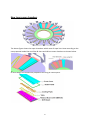
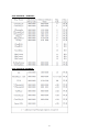
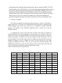
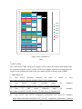
1
European Organization for Nuclear Research Indian Summer Students 2014 Internship Report Indian interns at CERN With Rolf-Dieter Heuer Director General, CERN & Archana Sharma Physicist, CERN Foreword What a great time to be a student of particle physics, however young you are and from wherever in the world you may hail. Every year, CERN welcomes summer students, people typically in the third year of their undergraduate studies, who come here to work with our scientists at the cutting edge of human knowledge. For the last few years, students from our Member States have been joined by young people from other countries, among them India, and it’s a pleasure for me to introduce the work of the 2014 cohort in this volume. CERN is celebrating its 60th anniversary this year. Sixty years of science for peace, over which time we’ve seen our membership grow from 12 countries to 21, and our user community expand to embrace over 100 nationalities. India has long been among the most important of CERN’s non-European partners, contributing to the intellectual life of the laboratory, and also to our infrastructure through the provision of specialised magnets for the LHC, to cite just one example. Indian physicists were involved with the discovery of the Higgs boson, a particle belonging to a family of particles that takes its name from the great Indian physicist Satyendra Nath Bose. So important was his work that one physics professor famously quipped to a student: “You don’t know who he was? Half the particles in the universe obey him!” The discovery of the Higgs boson and the confirmation of the underlying Brout-Englert-Higgs mechanism makes it a great time to be involved with fundamental physics as we embark on a new chapter in humankind’s understanding of the universe. I wish the Indian summer students whose work you can read here all the very best at the start of their careers, and I look forward to strengthening scientific and technical collaboration between CERN and India as we look forward to the next 60 years. Rolf-Dieter Heuer, CERN Director General Indian Summer Students at CERN 2014 Amal Ankit George Himanish Mayank Nancy Nabeel Mrinalini Eshan Priya Sachin Sudeep Rahul Sandipan Pronoy Saswata Contents Student Institute Supervisor Page No. 1. Amal Roy NIT Goa Jared Sturdy 1 2. Sudeep Maity NIT Goa Jared Sturdy 1 3. Ankit Verma IIT Indore Antti Onnela 9 4. Eshan Yash Sharma IIT Indore Jeremie Merlin 14 5. George Pius MIT Manipal Stefano Colafranceschi 18 6. Himanish Ganjoo BITS Pilani Stefano Colafranceschi 25 7. Nabeel Abdulla NIT Calicut Stefano Colafranceschi 25 8. Mayank Gaurav NIT Durgapur Antonio Conde Garcia 33 9. Mrinalini DTU Jared Sturdy 38 10. Nancy Nayak NIT Durgapur Anne Dabrowski 44 11. Priya Prasad NIT Durgapur Anne Dabrowski 44 12. Pronoy Sebastian NIT Calicut Stefano Colafranceschi 54 13. Rahul Sinha NIT Durgapur Antonello Di Mauro 59 14. Sachin Varghese NIT Goa Brian Dorney 64 15. Sandipan Das NIT Durgapur Giacomo Volpe 71 16. Saswata Das NIT Durgapur Jean- Pierre Revol 77 Study and Development of GLIBv3 application framework in XDAQ system of CMS -Sudeep Maity and Amal Roy B.Tech students, National Institute of Technology Goa Indian Summer Intern 2014 Cern, Geneva Supervisor - Jared Sturdy Abstract: - The project emphasizes on studying the role of GLIB in DAQ system of CMS and developing a web user interface for accessing the internal readout registers of GLIB in XDAQ (Xdaqgem) environment. Introduction The Gigabit link Interface boards (GLIB) is a field-programmable gate array (FPGA) based system. It is an evaluation platform and an easy entry point for users of high speed optical links in high energy physics experiments. Its intended use ranges from optical link evaluation in the laboratory to control, triggering and data acquisition from remote modules in beam or irradiation tests. The GLIB is a double-width Advanced Mezzanine Card (AMC) conceived to serve a small and simple system residing either inside a μTCA crate or on a bench with a link to a PC and it is based on a high-performance Virtex-6 FPGA. The GLIB can interface with four SFP+ transceiver modules, each operating at bi-directional data rates of up to 6.5Gbps. This performance matches comfortably the specifications of the GBT/Versatile Link project with its targeted data rate of 4.8Gbps. 1 The GLIB I/O capability can be further enhanced with two FPGA Mezzanine Cards (FMCs).The two high-pin-count FMC sockets each provide up to 80 user-specific differential I/O pairs directly connected to the FPGA as well as two differential clock inputs and two differential clock outputs. The primary FMC also provides four optional 6.5Gbps transceiver lines, thus allowing extending the high speed serial I/O capability. Figure 1: Image of GLIB final prototype (GLIBv3). The image above is of GLIBv3 board highlighting its major components i.e. the Virtex-6 FPGA, the AMC connector, the cage for 4 Small Form Factor Pluggable Plus (SFP+) optical modules, the FMC sockets, the SRAM devices, the socket for the GLIB user manual, a Module Management Controller (MMC) mezzanine card and the 1000Base-T interface (cabled Gigabit Ethernet). 2 GLIB part of GEM Hardware • On-detector electronics (VFAT ASICs) send data to an opto-hybrid, • Which is responsible for sending signals via the optical links to the front-end electronics(Gigabit Link Interface Boards) are housed in a uTCA crate. • GLIBs communicate with the chamber electronics via optical fibers and sends data to the central DAQ. • A uTCA Controller Hub connects to a PC and provides control of the GLIB through software over UDP via a protocol called IPBus (developed by CMS). Figure 2: GLIB and MCH 3 GLIB System Registers and their address Addr Name Description Type 0x00 Board_ID The board identifier code RO 0x01 System_ID The system identifier code RO 0x02 Firmware_ID The firmware date and version number RO 0x03 Test_Reg Register for test purpose only RW 0x04 Ctrl Control the external clocking circuitry RW 0x05 Ctrl2 Flash control RW 0x06 Status Status from various external components RO 0x07 Status2 Currently not used RO 0x08 Ctrl_SRAM SRAM interface: Control RW 0x09 Status_SRAM SRAM interface: Status RO 0x0A SPI_txdata SPI interface: data from FPGA to clock synthesizer RW 0x0B SPI_command SPI interface: configuration (polarity, phase, frequency etc.) RW 0x0C SPI_rxdata SPI interface: data from clock synthesizer to FPGA RO 0x0D I2C_settings I2C interface: configuration (bus select, frequency etc.) RW 0x0E I2C_command I2C interface: transaction parameters (slave address, data to slave etc.) RW 0x0F I2C_reply I2C interface: transaction reply (transaction status, data from slave etc.) RO 4 Building a Web GUI for accessing the GLIB registers in XDAQ (xdaqgem) XDAQ XDAQ is a framework designed specifically for the development of distributed data acquisition systems. It provides platform independent services, tools for local and remote inter-process communication, configuration and control, as well as technology independent data storage. XDAQ is a middleware that eases the tasks of designing, programming and managing data acquisition applications by providing a simple, consistent and integrated distributed programming environment. The framework builds upon industrial standards, open protocols and libraries. XDAQ in CMS control system 5 Purpose: The main idea behind the development of the xdaqgem software is to provide a SOAP interface for communication between the glib and the computer. It should provide the tools for exchanging the monitoring information between the applications, tools facilitating the GUI development – in case of the TS based on the AJAX technology, Tools for (remote) logging, monitoring the application state, and many, many others things. Tasks Required: In order to develop the XDAQ application for controlling the given hardware component subsystem we must: – customize some framework classes – define needed SOAP interface – define GUI – create the custom code for controlling and monitoring the hardware. Languages to be used: -C++ -Html and CSS -JavaScript -xml Approach: To develop a basic web interface that interacts with the user and can be used to exchange the version information between the user and the GLIB using C++ code. This code included all the html and JavaScript codes which were required to develop a web-based graphical user interface which was wrapped under CGICC wrapper. Xml files and make files were simultaneously developed for the build of the program. This program was put on the server side and the user was made able to write the versions onto the GLIB registers and the written values were also read back from the registers to ensure its reliability. 6 Figure Below is a sample idea of the web based reading and writing interface. Experience It has been a great experience to work with one of the sharpest minds of the world who work together as a team to discover the past, present and future of the mankind. These two months helped us academically to enrich ourselves with vast knowledge as well as improve ourselves to be part of a team, work with others and share and learn many new things. It also helped us in facing new challenges without fear of failure and step up in crucial situations and take responsibilities when required. We hope we have utilized this golden opportunity to its maximum and hope to build up ourselves on these experiences. 7 Acknowledgement We would like to thank our mentor Mr. Jared T. Sturdy who guided us through the whole project and constantly helped us in the same. Our heartfelt thanks to Dr. Archana Sharma for giving us a golden opportunity to be part of this wonderful program. We would also like to thank all our fellow members who were part of this group for all their support and encouragements throughout this program. I also thank Dr. G.R.C Reddy, Director NIT Goa and Dr. Venugopal Reddy, Faculty-in-charge, CERN Summer Students Program for all their help in making this internship possible. Finally I would like to thank all the CERN members for a giving a kind and lovely environment throughout the program and for helping us in all possible ways to make our stay a great experience for us. REFERENCES 1. https://espace.cern.ch/project-GBLIB/public. 2. https://twiki.cern.ch/twiki/bin/view/XdaqWiki/WebHome. 3. https://twiki.cern.ch/twiki/bin/view/CMSPublic/WebHome. 4. https://twiki.cern.ch/twiki/bin/view/CMSPublic/WorkBookCMSSWFramework. 5. https://twiki.cern.ch/twiki/bin/view/MPGD/GEMDAQSoftwareFirmware. 6. https://twiki.cern.ch/twiki/bin/view/MPGD/Electronics. 7. P Vichoudis et al, “The Gigabit Link Interface Board (GLIB), a flexible system for the evaluation and use of GBT-based optical links”. 8 Project Report of Summer Internship CMS, Tracker Upgrade CERN (European Organisation for Nuclear Research) 21/05/204-24/07/2014 Geneva Switzerland CMS TRACKER PHASE-2 UPGRADE: ANALYSIS AND MATERIAL SELECTION FOR CMS TRACKER BPS SUPPORT STRUCTURE Ankit Kumar Verma Discipline of Mechanical Engineering, School of Engineering, Indian Institute of Technology Indore, Madhya Pradesh453446 India [email protected] Antti Onnela (Supervisor) PH-DT CMS, CERN (European Organisation for Nuclear Research), Geneva Switzerland [email protected] ABSTRACT In this report, analysis of the Ring- which is the basic structural element of the proposed CMS Tracker BPS sub-detector is done to ensure the sufficient stiffness and strength of a support. Further, material selection for CMS Tracker BPS (Barrel with PS Module) support structure is concluded. This Inner barrel part of the Phase 2 upgrade tracker contains PS Type Modules which are mounted in tilted trajectory. The support structure is supposed to be homogenous made up of composites in order to provide the necessary strength so that the 2S and PS type of modules can be mounted. The deformation in support structure should be as minimum as possible in order to place the module on predefined orientation. Directional deformation in X, Y and Z direction is measured to understand the pattern of deformation. Further, thermal behaviour of ring is analysed as the support structure is supposed to be subjected to the range of temperature from -50° to +50°C. For detail report of this support structure, find my detailed analysis report on CERN sharepoint where analysis results of each and every case are discussed in details. surround it. As particles travel through the tracker the pixels and microstrips produce tiny electric signals that are amplified and detected. The tracker employs sensors covering an area the size of a tennis court, with 75 million separate electronic read-out channels: in the pixel detector there are some 6000 connections per square centimetre The CMS silicon tracker consists of 13 layers in the central region and 14 layers in the endcaps. The innermost three layers (up to 11 cm radius) consist of 100×150 μm pixels, 66 million in total. The next four layers (up to 55 cm radius) consist of 10 cm × 180 μm silicon strips, followed by the remaining six layers of 25 cm × 180 μm strips, out to a radius of 1.1 m. There are 9.6 million strip channels in total. Keywords: CMS Tracker, PS Module, BPS INTRODUCTION The CMS tracker records the paths taken by charged particles by finding their positions at a number of key points. The CMS tracker is made entirely of silicon: the pixels, at the very core of the detector and dealing with the highest intensity of particles, and the silicon microstrip detectors that SUPPORT STRUCTURE CONSTRUCTION AND ASSEMBLY: Tracker BPS has cylindrical layers each of which is individually made up of rings aligned in a line. Each Ring has 1 or 2 cooling pipes and support plates for holding the 2S and PS modules in the 9 considering two possible cases of loading- in plane and out of plane gravitational acceleration. 1.2) Analysis of Ring with triangular parts and support plates while considering both possible cases of loading – in plane and out of plane gravitational acceleration. 1.3) Thermal Analysis of Ring structure with support plate and triangular parts. required pattern. To reduce the number of the modules while maintaining the same geometrically coverage area, the proposed BPS geometry uses a tilted module arrangement. Modelling in ANSYS Workbench 15: Only self-weight of ring is considered. (g= 9.8066 m/s2). Cooling pipes are neglected. Weight of Modules are neglected. Deformation, stresses due to thermal difference is neglected. Ring is symmetrical along ZX plane (Fig.). Properties of Foam and Skin Material are assumed to be orthotropic. Simulations are performed considering Environment Temperature= 220C. Carbon skins are modelled as skin shell to increase the calculation efficiency. 2S module PS Module To fulfil this requirement a support structure is designed which can offer a flexibility to glue the modules at per required angle. Results: K13D2U/Cyanate Ester/UD-0.012, t=.72 mm 1) As shown in Fig1 that point 1, 2 and 3 are fixed one, so the magnitude of deformation is less in nearby area of fixed points and rest of the part has not much significant amount of deformation. The maximum deformation which is possible if acceleration due to gravity is working in the plane of the ring is 2.6 µm which is absolutely in the safe limit. And when acceleration due to gravity is considered to be out plane of plane, then the possible maximum deformation is .8 µm 2) The maximum von-mises stress is produced is near the fixed points which is .533 MPa which is also under the same limit and if acceleration due to gravity is working out of plane of ring then maximum possible stress is 4.8 MPa. In the current layout, the modules closest to the centre are horizontal and supported by flat plates, while those away from the centre are supported by Rings with modules tilted at angles ranging from 35 to 75 degree. Ring is the basic structure of this support structure for PS and 2S Module M76 (HexPly M76 UD M55J), t=.52 mm 1) If acceleration due to gravity is working in plane the maximum deformation possible is .11 mm while if g is working out of plane then maximum deformation possible is .115 mm. which is of course away from the fixed point. 2) The maximum von-mises stress possible if acceleration due to gravity is working in plane is 4.4 MPa while if g is working out of plane then maximum possible von-mises stress is 4.49 MPa. Analysis of the structure is done with three different carbon skins (K13D2U Vs M55 Vs T800) and keeping same foam core material (Airex 80.82).Further deformations both in plane and out of plane are considered. For the detailed analysis of CMS Tracker BPS is divided into three parts1.1) Analysis of Ring neglecting the cooling arrangements, triangular parts and support plates M76 (HexPly M76 UD M55J), t= 1.05 mm 1) If acceleration due to gravity is working in plane the maximum deformation possible is .114 mm while if g is working out of plane then maximum deformation possible is .1145 mm. which is of course away from the fixed point. 10 2) The maximum von-mises stress possible if acceleration due to gravity is working in plane is 4.45 MPa while if g is working out of plane then maximum possible von-mises stress is 4.45 MPa. Comparison of Analysis Results: Above is the analysis result from ANSYS Workbench 15 when in plane acceleration due to gravity is provided as loading plus the density of the support plate is increased to compensate the weight of Module which are here considered as of 35g. This ring structure is provided three fixed point and support plates and carbon skins are modelled as shell. In this analysis result, skin of K13D2U is used which shows the maximum deformation of 11.7 µm. Above is the analysis result of Ring with K13D2U as skin material but loading is provided as acceleration due to gravity out of plane. In this analysis the maximum deformation possible is .21 mm. It is clear from the graph, while using the same core material Airex 80.82 performance of skins are different depending on their mechanical and thermal properties. In case of the Cynate Ester the deformation is very less as compared to the other two skin used on the same core material but from economics point of view since the cost of Cynate Ester is much more as compared to those M76 ones, further the deformation is much significant and obviously it can fulfil our need. In M76 skins, that which has thickness 1.05 mm is preferred for its good Mechanical and thermal properties. Observations: The possible maximum total deformation, when acceleration due to gravity is in plane is 11.7 micrometre which is on support plate. Deformation on the support plate should be as low as possible so that modules can be placed at predefined orientation and the maximum possible total deformation when acceleration due to gravity is out of plane is 0.19 mm. 1.3) Analysis of Thermal Behaviour of Ring Structure: The support structure of CMS Tracker BPS is exposed to very adverse condition especially the temperature ranging from -50 to +50˚C so coefficient of thermal expansion creates some extra deformation and fatigue to the support structure along with loading and selfweight. Modelling is done same as earlier only thermal condition is included additionally. In thermal condition, full body is kept at uniform temperature. For all three carbon skin the deformation due to selfweight and temperature variation is noted and plotted. 1.2) Analysis of Ring with support plates in ANSYS 15: Now the analysis is done with support plates with modules, again changing the different carbon fibre skins while keeping the material of foam core same. Further von-mises stress, total deformation, directional deformation in X, Y and Z direction are recorded. 11 Observation: Above is the graph of Equivalent Von-Mises stress Vs Temperature. While using K13D2U as carbon skin type with Airex as Foam Core, when the in plane acceleration due to gravity is provided as loading, the maximum possible equivalent stress varies linearly with respect to temperature. It first decreases linearly until it crosses the environment temperature of 22°C, then it increases linearly. In case of K13D2U, the maximum possible equivalent stress is 5460 MPa at -50˚C while in case of M55 fibre, the maximum possible stress is 3885 MPa whereas with T800 skin show the maximum possible stress is 4220 MPa. This proves that K13D2U can withstand more stress as compared to other two carbon fibre skins. So, keeping all the aspects in mind, no doubt K13D2U is the choice of skin material for this type of support structure keeping Airex 80.82 as foam core material but it is economically very much expensive so now it depend on how much deformation is acceptable and in this respect M55 fits best. The above plotted graphs are of total deformation Vs temperature when the in plane loading (acceleration due to gravity) is provided. Since the coefficient of Thermal Expansion is negative for all the carbon fibre skin so on increasing the temperature below environment temperature, deformation goes down but as it crosses the environment temperature, the total deformation increases in linear manner. For carbon Fibre skin- K13D2U, an in plane acceleration due to gravity causes the maximum total deformation of .00046 m while for skin M55, same type of loading gives the maximum deformation of .0045 m and for skin T800 the maximum deformation possible is .0078 m. References: CERN SharePoint: 1) CMS Barrel PS Tracker Mass Calculation 2) Material Evaluation for CMS Barrel PS Tracker Support Rings 3) CMS Tracker Phase 2 Upgrade: Analysis and Material Selection for CMS Tracker BPS Support Structure by A. Verma 12 ACKNOWLEDMENT I would like to express my deepest appreciation to my supervisor Dr. Antti Onnela who has attitude and the substance of genius. He continually guided me and extended his ideas to solve the engineering problems. Without his guidance and persistent help this research work would not have been possible. I would like to express my profound gratitude to Dr. Archana Sharma who opened world of physics for me, motivated and guided me throughout the research work. She explained and demonstrated the CMS detector especially Tracker which helped me to understand the significance of my role in Design and Analysis team, CMS Tracker. I am really grateful to all my colleagues Duccio Abbaneo, Giovanni Bianchi, Antonio Conde Garcia, Jaakko Esala, Alan Honma, Mark Kovacs, Stefano Martina, Stefano Mersi, Pierre Rose and Kamil Cichy who always guided me through their great ideas and experiences. In the last, I extremly grateful to CERN and IIT Indore whose joint effort gave me the best ever learning experience, provided the inspiring atmosphere and a fantastic platform to prove and use my skill in best and effective manner. 13 CERN Summer internship – 2014 Report Wireless Environment Sensor By - Eshan Yash Sharma IIT Indore, India Supervisor - Jeremie Merlin Introduction The aim of this project is to make a wireless environment monitor that can measure various environmental conditions like temperature, pressure, humidity and particle count. This monitor has been constructed for use at clean room of TIF, CERN. Our environment monitor senses the various parameters, translates it into meaningful message and transmits it over radio frequency; the other part of the monitor consists of a RF receiver connected to a small sized computer. This small computer translates the received message into our language and then plots it on a TV screen. Sensors We have used temperature, pressure and humidity sensors. These sensors send voltage signal in accordance with the physical conditions. We have calibrated them by referring to their datasheets. We use mathematical equations to convert their signal into decimal numbers. The working of these sensors and their calibration are as follows: Temperature sensor: LM 335 According to its manufacturers it operates over a current range of 400μA to 5 mA. When calibrated at 25°C it has typically less than 1°C error over a 100°C temperature range. The conversion of sensor voltage into temperature is as follows: 𝑇= 𝑇𝑜 ∗ 𝑉𝑟𝑒𝑎𝑑 ∗ 𝑠𝑡𝑒𝑝 𝑐𝑜𝑛𝑣𝑒𝑟𝑡𝑒𝑟 𝑉𝑜𝑢𝑡 Here T is temperature, Vread is the voltage signal from sensor, T o is the temperature at which sensor is calibrated and Vout is the voltage output at T = To .In our case, To = 25 ͦ C Vout = 2.9815 V Step converter = 0.004882 14 Pressure sensor: MPXA 6115A It is a piezoresistive, monolithic, signal conditioned, silicon pressure sensor. It has a range from 15 kPa to 115 kPa. It has 8 pins out of which we use three, namely, supply voltage (Vs), ground (Gnd), and output voltage (Vout). The output signal is converted as: PressMaxPositive = ((VoutPressure/5.25 + 0.095)/0.009)+(1.5*0.009*5.25) PressMaxNegative = ((VoutPressure/4.75 + 0.095)/0.009)+(1.5*0.009*4.75) PressMinPositive = ((VoutPressure/5.25 + 0.095)/0.009)-(1.5*0.009*5.25) PressMinNegative = ((VoutPressure/4.75 + 0.095)/0.009)-(1.5*0.009*4.75) Pressure = (PressMaxPositive+PressMinPositive+PressMaxNegative+PressMinNegative)/4 VoutPressure = Vout * step converter Humidity Sensor: HIH-4000 This sensor provides the value of Relative Humidity (RH). It has three pins supply voltage (Vs), ground (Gnd), and output voltage (Vout). Humidity is affected by temperature. So, we consider temperature in our calculation of humidity from the observed voltage signal. The mathematical equation is as follows: Humidity = 𝑉𝑜 5 1 1 − 0.16 ∗ 0.0062 ∗ 1.0546 −0.00216 ∗𝑇 Here, T = temperature (observed by temperature sensor) Vo = Vout *( step converter) Transmission: The sensors used for measuring physical parameters are connected to Arduino Mega 2560 microcontroller. The voltage signal from these sensors is received and converted to meaningful data by arduino using the equations mentioned in the previous section. We use RF 433 MHz transmitter and receiver for transmitting information from sensors. The delay between every two bits is 1 millisecond. Message encoding The first step is to convert the decimal value into binary. We have used a function in arduino for this purpose. Next, we have to solve the problem of incorrect transmission or noise. Noise can be present due to several factors and we have to make the system capable of identifying the relevant signal. For this, we are using: Manchester coding Parity bit Sequential transmission of keys 15 Under Manchester coding, bit 1 is expressed as 10 and bit 0 as 01. The parity bit is assigned the value 1 if the message is an even number and is assigned value 0 if the message is odd. Lastly, the message is sequentially transmitted as: Sensor Key Sensor Value Parity bit Sensor key As an example let’s suppose the value of temperature is 22.12 C and the key for temperature sensor is 100. We multiply the sensor value by 100 to include the first two digits of decimal part. The binary equivalent of 100 is 01100100 and is 0000100010100100 for 2212. Parity bit for 2212 is 1. So, the message transmitted will be: 0110100101100101 01010101100101011001100101100101 1 0110100101100101 Thus the message length for 1 sensor data is 65 bits. The data of the three sensors is sent one after the other with their respective keys and parity bit of message. Reception at Raspberry Pi: The transmitted signal is received by RF receiver operating at the same frequency as the emitter i.e. 433 MHz. The receiver is connected to a Raspberry Pi which is a credit card size computer. We use one of its 7 General Purpose Input Output pins (GPIOs). Fig. 1 Raspberry Pi Fig. 2 Arduino and sensors 16 Reception Code: The code in RPi for reception is written in C++. It reads from RF receiver and stores a particular number of values (say, 516) in an array known as buffer. This buffer is then analyzed for information. The algorithm for identifying data in buffer is: 1. 2. 3. 4. 5. 6. 7. Search for the key of sensor Skip the bits having data and parity bit Check if the key sent at the end of message is available If both ending and starting key are detected then we analyze the bits in between Calculate the value of the data and check if it is even or odd Now compare the result obtained above with parity bit If the two match then the code declares that data has been received Storing data: All the data obtained in the previous section is saved in a text file having the name ‘date’_cleanroom.txt where ‘date’ is the actual date of that day in the format yyyymmdd. Display of data graphs: All the data received is displayed on an LCD TV in real time. For this we are using Gnuplot. It is a portable command-line driven graphing utility for Linux, OS/2, MS Windows, OSX, VMS, and many other platforms. Gnuplot can generate two- and threedimensional plots of functions, data, and data fits. On the screen we display graphs of temperature, pressure and humidity sensor values along with the last value received. We display the present time as well. The display looks like Fig. 3 Fig. 3 Display 17 Summer Internship Report George Pius Perangatt 29-Aug-14 18 Aim The object of our project was to complete the required quality control procedure and assemble four resistive plate chambers (RPCs). Introduction During our stay at CERN, the Large Hadron Collider was undergoing a long shutdown (LS1). This allowed for certain upgrades to be implemented in the CMS experiment. The upgrade required the installation of a fourth layer of RPC detectors in the compact muon solenoid thereby improving the muon tracking system and its ability to cope with higher luminosity. We were assigned for the construction of four RPCs which would be needed in the installation of the new layer. Procedure QC2 The first quality control procedure is called QC1 and is carried out by the manufacturer. The second quality control procedure (QC2) was carried out by us. QC2 is similar to QC1; the purpose of it is to ensure the quality of the gaps and it and entails the following tests: a visual inspection, gas leak test, spacer test, and the measurement of dark current and stability over a period of 3 days. Visual Inspection: This test looks at the following features of the gap: - Air bubbles: the fewer the air bubbles the better as if these air bubbles are close to the edge it can serve as a path for charge to build up and transfer to materials nearby. - The label: both sides have to be labeled correctly as the high voltage and ground sides respectively. - The cable and its connections: the cables must have the wires connected to the corresponding high voltage or ground side and must not be damaged. 19 - The PET coating on both high voltage and ground sides: the coating must be even with minimum gaps or deformations. - Glue excess: sometimes an excess of glue is present because of the application of the PET coating. This is undesirable as it impairs the flat and even surface that the PET coating is supposed to produce. - Gas inlets: these are very important as they serve as an access point that allows us to pressurize the gaps. They are quite fragile so while moving the gap caution must be taken to insure the inlet is not damaged and remains intact. - The sides of the gap must also be checked for any signs of damage. Leak test Once the visual inspection is completed, the gaps can now be leak tested. This is done by pressurizing the gap and observing it over a period of 10 minutes. A computer monitors the pressure and the pressure drop after the required time is noted. This helps calculate the leak rate of the gap. The gaps are leak tested twice, both at approximately 5 millibar and 15 millibar. A leak rate of up to 0.3 millibar per second is accepted. 20 Spacer Test The spacer test is done to make sure that the spacers that separate the two layers within the gap are placed in the correct positions. In order to do this, a template with the correct positions of the spacers is placed over the gap while it is pressurized. Pressure is applied even further on the gap by pressing down on certain points. While pressing a marked area, there should be no significant change in the pressure due to the fact that there should be a spacer at that point. However, any other area while pressed down should show a considerable change in the pressure. All marked areas are pressed down and if there is no significant change in pressure then it confirms that spacers are correctly positioned. High Voltage Test This is the last element of the QC2 procedure. The gaps are placed in a stand and a high voltage current is passed through them and leakage current is measured; this process lasts 3 days. There are two distinct parts to the test. In the first, the voltage is varied from 0 to 10 kilovolts and the leakage current is measured. In the second part the voltage is kept constant at 6 kilovolts and 9.7 kilovolts and it is checked whether the leakage current is constant while voltage is constant. 21 Chamber Construction Now that QC2 has been completed, the gaps are removed from the stand and assembly of the chamber can now begin. The following are the steps for assembly of the chamber - First the chamber is opened and the bottom is lined with a copper sheet. - The bottom gap is prepared by attaching plastic pipes (ones that have already been cut and bent appropriately) to the top right and bottom left gas inlets of the gap. They must be heated first in order to attach them to the gas inlets. The remaining inlets are blocked using more pieces of small plastic pipe (half the pipe is filled with glue so once the other end is attached it serves as a cap that blocks the gas from escaping). - The copper sheet is cleaned and the gap can now be placed inside the chamber. Afterwards the gap should be checked to make sure it is aligned correctly. Once the alignment is correct the supports are fixed in and the gap surface is also cleaned. - Next a readout strip is cleaned and installed over the bottom gap. - The top gaps are prepared in a similar fashion as to the bottom gap. Afterwards, the top wide and top narrow gaps are placed carefully inside the chamber and the alignment is once again checked. - Once the top gaps are inside the chamber the two pairs of adjacent gas inlets must be connected via a U-shaped plastic pipe in order for the two to function as one body when storing gas inside. The plastic pipes are attached to the appropriate gas inlets and the remaining inlets are blocked. - The gaps are leak tested again within the chamber to make sure they are still functioning properly. - The wires are labeled in order to avoid confusion once the chamber is closed. - Two separate copper sheets are placed over the top gaps. - Next the cables are soldered to the readout strip and ground pins are soldered to the copper sheet. - After the soldering has been completed, the cover can be placed and the chamber can be closed. - Next the patch panels for the gas pipes, high voltage cables and the cooling circuit are mounted. 22 - The chamber undergoes one last leak test as an extra precaution. - The cooling circuit is the attached and flat cables are used to connect cables and the FEBs. - Finally an aluminum covering is attached to protect the cooling circuit and the chamber is completed. Conclusion During my stay at CERN as an intern, I had the opportunity to assist with the second quality control procedure and the assembly of the chambers. However the process had not been completed yet; QC3 has to be carried out next. It repeats some of the elements from QC2; however, the focus of the procedure is the use of a cosmic stand to evaluate detector performance parameters such as efficiency, cluster size and noise. Once this has been successfully completed the chamber is subjected to QC4 which involves powering up the chambers and monitoring their stability. After this the chamber is finally ready to be installed. 23 Acknowledgements Firstly I would like to thank Mr. Jianxin Cai for teaching me the aspects of his work concerning RPCs at CERN and allowing me to assist. I would also like to thank Stefano Colafranceschi for his role as my supervisor and his continuous guidance that helped throughout my stay at CERN. Last but not least I would like to express my sincere gratitude to Dr. Archana Sharma for providing me with this amazing opportunity which led to an invaluable experience. 24 REPORT S U M M E R I N TE R N S HI P , J U N E - J U L Y 2 0 1 4 HI M A N I S H G A N J O O , B I R L A I N S T I TU T E O F T E C H N O L O G Y A N D S C I E N C E , P I L A N I , I N D I A N A B E E L M A B D U L L A H, N A T I O N A L I N S T I TU T E O F TE C HN O L O G Y , K O Z H I K O D E , I N D I A SUPERVISOR: STEFANO COLAFRANCHESCI OBJECTIVES ASSEMBLY AND TESTING OF RESISTIVE PLATE CHAMBERS FOR THE RE4 LAYER OF MUON DETECTORS FOR THE COMPACT MUON SOLENOID. 25 MUON DETECTORS IN THE CMS The Compact Muon Solenoid experiment uses Resistive Plate Chambers as detectors and trigger systems for muons produced due to p-p collisions in the Large hadron Collider. Muons are relics of most important particle-particle reactions, for instance, the Higgs boson candidate decays into four muons. In the CMS, drift tubes and Cathode Strip Chambers are used to track muons, and RPCs are used for triggering and reconstruction. Events occur at the high rate of 40 MHz in the experiment, and the first level of the triggering system is used to filter out events of interest. RPC layers form part of this triggering system, covering the barrel and the endcap of the detector. In accordance with the full recommendations of the CMS Technical Design Report, during Long Shutdown I, the process of adding a fourth layer, RE4 in the muon detector system, began. The designated new layer has two rings of 36 chambers each, to be placed in the endcap region. 26 RESISTIVE PLATE CHAMBERS Resistive Plate Chambers are a type of gas detector that is used to detect charged particles by their effect of ionization of gases. They were introduced by Santonico and Cardarelli in 1981, as a simpler alternative to spark chambers. They consist of a pair of parallel plates made of a material of high resistivity, with a gas filled within the spacing between the plates. The parallel plates provide a uniform strong electric field, due to high voltage applied across them, within the spacing. When a charged particle passes through the spacing, the gas gets ionized. The strong field propels the generated electrons towards the plates. These free charge carriers lead to electron avalanches, going on to deposit an electric discharge on the plate surface. The plates are highly resistive, and this ensures that the deposited discharge does not dissipate immediately. The spot at which the discharge is deposited remains blind for a certain time after deposition. 27 The deposited charge leads to an induced charge outside the plate, on regions covered by copper strips. The induced charge on these copper strips generates electrical signals, which are then passed on to the readout electronics for processing. Formation of an electron avalanche upon ionization, in the presence of a uniform electric field. Readout electronics are interfaced to readout strips, that register the location at which the induced charge appears, thus helping in tracking muons. The readout electronics contain discriminator circuits which send signals to link boards through copper cables. Link boards then provide services for data compression and conversion to optical signals sent to the CMS counting room. In our applications for the CMS, the RPC gaps are made out of two parallel layers of bakelite. They are filled a Freon gas mixture. The surfaces are painted with graphite to form high-voltage and ground electrodes on the two sides. 28 For our purposes, we need detection chambers that can withstand a high number of hits, due to high event generation rate of collisions. Also we need less noise, while the time resolution should be high. For this, RPC chambers with two gaps are usually used, with common readout strip sheets. Bakelite surfaces are also coated with linseed oil to reduce noise. The gap configuration in one chamber is: top-wide, top-narrow, and bottom gaps, put in two layers with intervening copper readout sheets. The front-end boards are specially designed to transmit muon hit signals. Analog signals from the strips are put through two discriminator circuits working in tandem. One selects signals with levels above the threshold, and the other detects the peak of the signal to discern the hit of the muon. This processing is done by a customized ASIC chip with 8 channels, one for each strip. The resolution for determining the hits on the chambers is decided by the width of the strips. In the endcaps, the RPC chambers form four radially-oriented discs, with 36 chambers each. 29 TESTING The CMS muon labs were charged with assembling and testing the RPCs for RE4. The gaps and assembled chambers go through a series of physical, electrical and run tests. The bottom gaps as seen placed in a chamber PRESSURE AND SPACER TESTS The gas gaps have four nozzles, and these are used to fill a test gas at 5 mbar and 15 mbar pressure, to check for significant pressure deviations due to gas leakage. The maximum deviations in a period of ten minutes are 0.4 mbar. Input station for pressure leak test 30 Post this, a manual spacer test is done to ensure all spacers are in place, and rigid, by placing a spacer map on the gap and pressuring spacer points to check for high pressure deviations. In addition, physical inspections are conducted to check for unnaturally large bubbles, broken coatings and other apparent shortcomings. ELECTRICAL TESTS The gaps tested above are assembled in a gap stand, where their surfaces are put to high voltage. The voltage values vary from 3 to 10 kV, over the 2 mm gap spacing. The tests check for leakage current for the applied voltages in two ways. One part checks the leakage for a range of voltage values, and the next step is to check leakage at a high voltage value maintained for a long time. Above: Gap stand for electrical testing. Below: Scatter plot, Voltage vs Leakage Current, Gap RE4/3-B123 31 COSMIC STAND Post assembly, the completed RPC chambers are assembled in the cosmic stand, which uses cosmic muons passing through the lab to conduct real-time tests on the detectors. The cosmic stand test runs for three to our days, and cosmic muon paths are tracked, with performance recorded and evaluated in real time. This test is complete with gas inputs and high voltage applied. It is a combined test of the final product. Above: Cosmic Stand at CERN Below: Final assembled chambers 32 Project Report CERN Summer Students Internship 2014 Name: Mayank Gaurav ([email protected]) Department of Mechanical Engineering National Institute of Technology, Durgapur Supervisor: Antonio Conde Garcia .................................................................................... Title: Designing of first full size Gem based Super Chamber Prototype for CMS. Introduction: The CMS muon system relies on three detector technologies: Drift Tubes (DT), Cathode Strip Chambers (CSC) and Resistive Plate Chambers (RPC) . The DT and CSC provide precision tracking functions, and RPCs provide fast trigger. During the CMS commissioning and construction, several concerns were raised on whether RPCs would be able to sustain the very hostile environment that will be created due to release of huge amount of particles in high energy collisions; it was decided not to instrument this area at all. Gas Electron Multipliers (GEMs) are an interesting technology for the future upgrade of the forward region of the muon system since they can provide precision tracking and fast trigger information simultaneously: moreover they can be designed with sufficiently fine segmentation to cope with high particle rates at LHC . Aim of the Project: This project covers the following topics in detail 1) 2) 3) 4) Designing of long Super chambers with new Gem Frame . Introduction of new vfats and subsequent changes in Readout. Introduction and study on GEB. Introduction of flanges in the structure 33 New Long super chambers The above figure shows the super chambers which were of equal size. Now according to the new proposed model there will be 18 short and 18 long super chambers as shown below. So accordingly first model was proposed consisting of various parts. 34 A brief description of parts • • • • • • Vfats: Very Forward Atlas and Totem (VFAT) chip. It is a complex digital part for data formatting and transmission. It resists radiations as well. It sends the collected data finally to the Optical Board. Gas Pipe: Transports the gas to be ionised. Readout: Electrons multiplied and transferred into the induction gap are collected and detected on a patterned printed circuit board called Readout. Optical Board: Sends the signal collected by the vfats to computer via optical cables. Spacers: It was used earlier to separate the gem foils. But new gem foils can be stretched. Cooling Pipe: It is used for cooling vfats and optical board. Generally one vfat generates 1 watt of heat .So total of 24 watts. Taking optical board and some extra total of 30 watts per chamber is assumed. Removal of spacers and including new GEM Frame (yellow) Introduction of new vfats and its arrangement With several new proposals, vfats (pink) were changed from rectangle to hexagon. The arrangement was changed accordingly taking into the considerations. Readout design slightly changed to be easily attached to outer frame and its outer dimensions changed keeping into account of the gem frame. 35 Introduction of GEB • • • • The new unit called geb is included in the design. It was specially designed to remove a large amount of cables that were emerging out in previous designs. It is present in contact with readout. Size of GEB is smaller by 24mm compared to readout. The figure below shows the arrangement of GEB with respect to readout. Introduction of Flanges Flanges or ear shaped structures were introduced to attach readout to the geb. It is present on sides of readout and geb and a total of six in number. Exploded view of the model 36 Further Proposed changes and discussions: The current model is still under discussion. With the change in vfat and its arrangement cooling is most important concern. Each of new Vfats generate 1 watt of heat and optical board 6 watt of heat. So (1*24)+(6)= 30 watts. So cooling system should be able to remove this amount of heat. The above project will be completed by 2015 and will be installed in CMS. GE2/1 project has started where one drift board will have chambers on both of its sides. It is a complicated project which has just begun. Conclusion: Designing of Triple Gem based Super chambers will enhance the particle detection capabilities of CMS to a great extent. Cooling is one of the important concerns since electronic chips and circuits are required to last during the long run. I have tried to include all my work and further progress of this project in this report showing all the necessary steps. Acknowledgement: I take this opportunity to express my profound gratitude and deep regards to my guide, Mr. Antonio Conde Garcia, for his exemplary guidance, monitoring and constant encouragement throughout the course of this project. The cooperation and guidance given by him time to time shall carry me a long way in the journey of life on which I am about to embark. I would like to thanks Mrs Archana Sharma, who served as the source of inspiration and continued to help me in tough situations. I am grateful to Dr. N.K.Roy and Dr. P Kumbhakar who made this project possible and supported us in whatever way he could. I am deeply thankful to my friends Saswata Das, Rahul Sinha, Nancy Nayak, Sandipan Das and Priya Prasad who helped me throughout my project . Last, but not the least, I thank my parents who are the ultimate source of energy and always embraced me with their countless blessings 37 CERN Summer internship – 2014 Report Development of Vfat interface application for XDAQ system of CMS Experiment SUPERVISOR – Dr Jared.T.Sturdy NAME - MRINALINI INSTITUTE - D.T.U., New Delhi INTRODUCTION: VFAT2 is a trigger and tracking front-end ASIC designed primarily for the TOTEM experiment. VFAT2 fits into the Totem electronics as shown in figure. The VFAT2 chip has 128 identical channels. It is a synchronous chip designed for sampling sensors at the LHC clock frequency of 40MHz. Each channel consists of a preamplifier and shaper followed by a comparator. If a particular channel receives a signal greater than the programmable threshold of the comparator a logic 1 is produced for one clock cycle only by a mono-stable. This logic 1 is written into the first of two SRAM (SRAM1). All other channels that do not go over threshold record a logic 0 in SRAM1. This occurs in parallel for all 128 channels at 40MHz. 38 At the same time a fast OR function can be used to set a flag which can immediately be used for creating a trigger. It is foreseen to have up to eight programmable sectors which can be flagged with the fast OR in this way. Triggering Function: Within TOTEM, VFAT2 will provide fast regional hit information to be included within the CMS First Level Trigger. Channels are grouped together to form sectors. A hit channel in a given sector will set an LVDS output assigned to that sector to a logic “1". The assignment of channels to sectors is programmable. There are 8 LVDS sector outputs labelled S1 to S8. Not all LVDS outputs need be used and the number sectors used can selected between 1,2,4 and 8. Once the number of sectors have been chosen the channel assignment to the sector can be made with different options. The options are determined by the requirements of the physics needed from VFATs used with the Roman Pots and VFATs used with the GEM detectors. Tracking Function: On receiving a LV1A signal, data corresponding to the triggered time slot is trans-erred to a second SRAM memory (SRAM2). The LV1A latency is not expected to exceed 6.4s (256 clock periods). Hence, SRAM1 is dimensioned 256 by 128. SRAM2 contains only triggered data. It is dimensioned to be 128 by 148 for data plus headers, hence VFAT2 can store up to 128 triggered events of data for all channels at any one instant in time. 39 VFAT2 will label the data with 3 headers. These are the Bunch Crossing number (BCN 12 bits), Event number (EN 8 bits), and the chip Identification number (ID 16 bits). The BCN is generated by a 12 bit counter (BC) that increments every clock cycle and is reset to zero on receiving a BC0 T1 command via LVDS. The EN is generated by an 8 bit counter that increments for every LV1. It is also reset by a BC0 command or the Clear signal. Both counters are cyclic and return to zero at the end of the counter range. As soon as SRAM2 contains data the Read cycle begins. During the Read cycle a Data Formatting block streams out a binary data stream to the GOL. The chip operates with a continuous write/read operation without dead time. VFAT part of GEM hardware: On-detector electronics (VFAT ASICs) send data to an opto-hybrid. Which is responsible for sending signals via the optical links to the front-end electronics (Gigabit Link Interface Boards) are housed in a uTCA crate. GLIBs communicate with the chamber electronics via optical fibers and sends data to the central DAQ. A uTCA Controller Hub connects to a PC and provides control of the GLIB through software over UDP via a protocol called IPBus (developed by CMS). 40 VFAT REGISTERS – PRINCIPAL: VFAT REGISTERS-EXTENDED: 41 XDAQ FRAMEWORK: XDAQ is a framework designed specifically for the development of distributed data acquisition systems. It provides platform independent services, tools for local and remote inter-process communication, configuration and control, as well as technology independent data storage. XDAQ is a middleware that eases the tasks of designing, programming and managing data acquisition applications by providing a simple, consistent and integrated distributed programming environment. The framework builds upon industrial standards, open protocols and libraries. WHY DO WE NEED TO BUILD AN INTERFACE FOR XDAQGEM? The main idea behind the development of the xdaqgem software is to provide a SOAP interface for communication between the VFAT and the computer. It should provide the tools for exchanging the monitoring information between the applications, tools facilitating the GUI development – in case of the TS based on the AJAX technology, Tools for (remote) logging, monitoring the application state, and many, many others things. REQUIREMENTS FOR MAKING AN INTERFACE: In order to develop the XDAQ application for controlling the given hardware component subsystem we must: – customize some framework classes – define needed SOAP interface – define GUI – create the custom code for controlling and monitoring the hardware. LANGUAGES: -C++ -Html and CSS -JavaScript -xml HOW DO WE MAKE AN INTERFACE? To develop a basic web interface that interacts with the user and can be used to exchange the version information between the user and the VFAT using C++ code. This code included all the html and JavaScript codes which were required to develop a web-based graphical user interface which was wrapped under CGICC wrapper. Xml files and make files were simultaneously developed for the build of the program. This program was put on the server side and the user was made able to write the versions onto the VFAT registers and the written values were also read back from the registers to ensure its reliability. 42 ACKNOWLEDGEMENT: I express my sincere and utmost thanks to Dr. Archana Sharma who gave me this opportunity to be a part of a project associated with CMS collaboration ,CERN. I am deeply indebted to my supervisor Dr Jared.T.Sturdy for his excellent guidance and constant inspiration. I thank him for his patience to sit down with me and explain to me the architecture of the interface and staying throughout the entire debugging process. He was very kind to answer all my doubts despite having a noncomputer engineering background( real admiration for him). I would also like to thank my colleagues who were part of this group for all their support and encouragements throughout this program and making it a memorable experience. And finally my parents, for being there for me always. 43 PROJECT REPORT OF SUMMER INTERNSHIP AT CERN 2014 Priya Prasad & Nancy Nayak Department of Electronics and Communication Engineering National Institute of Technology, Durgapur Supervisor: Dr. Anne Dabrowski Design of a LabVIEW program to control a Oscilloscope and High Voltage Power Supply Measurement 1. Abstract: In order to achieve the purpose of data collection, save and analyze, through the LabVIEW-based platform, this LabVIEW application is designed to control the oscilloscope by running it from a remote desktop which is not remotely connected from scope but have LabVIEW drivers installed. It configures the scope to take data from channels when there is an external trigger. It saves the data to csv format in a file. The Program mainly control amplitude, time scaling, trigger delay and trigger position, no. of channels enable, number of triggers to save, from the front panel (LabVIEW). 2. INTRODUCTION: CMS: The Compact Muon Solenoid (CMS) is a general-purpose detector at the Large Hadro Collider (LHC). It is designed to investigate a wide range of physics, including the search for the Higgs boson, extra dimensions, and particles that could make up dark matter. Although it has the same scientific goals as the ATLAS experiment, it uses different technical solutions and a huge solenoid magnet to bend the path of particles from collision in the LHC. LABVIEW AND NI-VISA : Alternative to the traditional instruments, a virtual instrument is an effective way to fulfill the improving technical requirements. The virtual instrument relying on computer technology, highlight the "software instrument" concept, User-self-definition and design, and the corresponding function can be designed according to the demand. And it can reach one or even multiple functions of traditional instruments in an integrated environment, and easy upgrade and expansion, cost effective .Now we have constructed a versatile virtual digital acquisition in the construction demand from the laboratory for measurement and control, which has been applied and received distinct effect. The Virtual Instrument Software Architecture (VISA) is a standard for configuring, 44 programming, and troubleshooting instrumentation systems comprising GPIB, VXI, PXI, Serial, Ethernet, and/or USB interfaces. VISA provides the programming interface between the hardware and development environments such as LabVIEW, LabWindows/CVI, and Measurement Studio for Microsoft Visual Studio. NI-VISA is the National Instruments implementation of the VISA I/O standard. NI-VISA includes software libraries, interactive utilities such as NI I/O Trace and the VISA Interactive Control, and configuration programs through Measurement & Automation Explorer for all our development needs. 3. SCOPE OF WORK We will have a setup for measurements using cosmic rays. A device will produce a trigger signal (an LVTTL pulse on a standard lemo cable) that will be connected to the dedicated trigger input of the scope. This device is controlled by another LabVIEW program. The features of the LabVIEW application that is written by us has the following features : It configures the scope to take data (one waveform each from any number of channels) when there is an external trigger. It saves the data to csv format in a file. (File name can be given at the front panel before execution of the program). We can enable or disable any number of channel from the four channels of the oscilloscope. We can control amplitude, time scaling, trigger delay and trigger position from the front panel. Number of triggers to save i.e. number of events. We can read the file even when program is running and if there is any error we can stop the execution instantly. The LABVIEW program can save the waveform file in such a way that it shows the date and time of each event occurred at the moment of triggering. Format of the waveform data saved is given below : Event1 0 08/07/2014 12:45:01 Channel1 0 0.859292 0.909106 0.884199 0.884199 -0.01245 0.024907 Channel2 -1.39479 -1.394792 -1.39479 -1.59405 -1.39479 -1.59405 -1.59405 Channel3 0.012454 0.909106 0.884199 0.896652 0.884199 0.012454 -0.02491 Channel4 -1.4197 -1.382339 -1.39479 Event 2 08/07/2014 12:45:02 -1.59405 -1.59405 Channel1 0.236617 0.896652 0.884199 0.896652 0.647582 -0.03736 0.024907 Channel2 -1.40725 -1.39479 -1.59405 -1.59405 1 -1.407246 -1.40725 -1.59405 -1.59405 -1.59405 Channel3 0.909106 0.909106 0.896652 0.884199 0 -0.01245 -0.01245 Channel4 -1.40725 -1.39479 -1.59405 -1.59405 -1.369885 45 -1.59405 -1.59405 Now charge of the signal is calculated using mathematical functions present in LabVIEW, and histogram is plotted. The purpose of plotting histogram is to calculate charge of the signal coming from Photo Multiplier tube. The reason behind calculating charge is that the output signal of a PMT is charge which is equal to number of photo electrons multiplied by the gain of the PMT. 4. EXPERIMENT: DESIGN OF LABVIEW CONTROL SYSTEM FOR LECROY OSCILLOSCOPE Before explaining the design part it is very essential to know how to connect scope with PC without remote connection. For the interface with Ethernet NI-VISA application is used. First the driver is installed. Then go for ‘Tools’>’Measurement & Automation Explorer’>’Devices and Interfaces’>’Network Devices’>’Create New VISA TCP/IP Resources’. Connect the device (oscilloscope) giving proper IP address and VISA name.‘Tools’> ‘Instrumentation’ > ‘Find instrument drivers’>If you are a user of National Instruments then you can ‘connect’ the Lecroy wave runner 104mxi oscilloscope to the PC via internet network, go to ‘scan for instruments’. It will automatically detect the oscilloscope. Then set visa resource name as given while creating new VISA TCP/IP Resources. (In our program VISA Resource Name is ‘BRM scope’).Configure all the channels with desired values, set the file path, enable channels which are required using boolean button given in front panel. Set values for amplitude, trigger position, time base, and number of events, bins. A. The design of control block diagram : The Program starts with a Case structure that helps us to enable the required channels. LecroyWaveSeries.lvlib:Initialize.vi takes VISA resource communication with the Device (LecroyWaverunner 104MXi-A) LecroyWaveSeries.lvlib:Configure Channel.vi channels to acquire waveform. name and establishes configures the common properties of the Open/Create/Replace File takes the file path from the front panel and create or replace the file (if already exists). After each iteration of while loop waveform data is placed in that file. Number of iteration of while loop is equal to number of events. For every eventLecroyWaveSeries.lvlib:Read Multiple Waveforms.vi waits for trigger and reads wave form data for all enabled channel whenever the trigger is received. This waveform data enters to case structure if there is no error. Inside the case structure there is a ‘for’ loop. In each iteration of for loop the waveform data is converted into two arrays, one containing the voltage of waveform and other contains charge. After the case structure a 2D array containing data of four channels is obtained which is exported to spreadsheet using Array to Spreadsheet String. 46 Output of while loop is a 2D array (event*number of channels) and it is transposed to get the following. Event 1 Event 2 Event 3 Channel1 • • • Channel2 • • • Channel3 • • • Channel4 • • • Using Index Array we get separate 1D arrays containing data of all events of each channel and is plotted in Histogram. B. Front Panel Design: Program front panel is a graphical user interface, it is VI's virtual instrument panel. Frontpanel is used to simulate the real instrumentation, Function is similar to the traditional instrument panel. Virtual instruments will gradually replace traditional instruments, and the virtual instrument is bound to play its important role in more fields. Virtual instrument front panel's controls are extremely similar to the traditional instrument panel's knobs, switches, buttons in the function and appearance. This makes the front panel intuitive and image. There are five Wavegraphs control the front panel, the four Wavegraph (Histogram CHx on the right side is used to display the Histogram of charge of the signal coming from PMT’s. The Wavegraph's function is very rich in the LabVIEW. User can choose the line style, color, data points by Plot legend. Using this feature, we can adjust the instrument waveform's display color, change the display of the data points. The front panel also set up the buttons and controls. In Front Panel we can give VISA Resource name, File in which waveform data is to be saved, Amplitude, Position, Time Delay, Number of Events, Vertical Coupling for each channel, enable or disable channel, Probe attenuation, Vertical offset, No. of bins for histogram plot etc. 47 Figure 1 Block Diagram in LabVIEW 48 Figure 2 Front Panel in LabVIEW after Simulation. 5. CONCLUSION: Design of the virtual instrument achieves function of controlling oscilloscope. Friendly software interface, simple operation, strong human-computer interaction, programming is easy, convenient and good scalability. It can be used for industrial, medical, control, and it is highly practical with the rapid development of computer technology and the measurement and control technology. 6. REFERENCES: 1. National Instruments, www.ni.com . 2. LabVIEW Application Builder User Guide, National Instruments Corporation. 3. National Instruments Discussion Forum. 4. Lecroy Waverunner 104 Mxi User Guide. 49 MEASUREMENT OF CAEN SY4527 POWER SUPPLY 1. ABSTRUCT: In this report measurement of high voltage power supply CAEN SY4527 has been done. SY4527 is a Universal High & Low Voltage Multichannel Power Supply Systems for Detectors. The System has been specifically designed to power the variety of detectors found in modern Physics Experiments, such as photomultipliers, wire chambers, streamers tubes, and silicon detectors and also to power Beam Halo Monitor. 2. INTRODUCTION: The system is modular and flexible enough to be appropriate both for major experiments where a large number of channels must be remotely controlled, and for test laboratories where simple manual operations on a limited number of channels are often desired. The modularity of CAEN SY4527 is appreciated over CAEN SY1527 for the easy maintenance of the CPU, fan unit and the power modules. This will make the maintenance, repair and upgrade much easier compared to the SY1527/2527. The tests show no significant difference in performance of the boards whether operated in the SY1527 or in the SY4527mainframe. Instead of CAEN Sy1527, CAEN SY4527 will be used to supply power to BHM in future. BEAM HALO MONITOR: A fast and directional monitoring system for the CMS experiment is designed to provide an online, bunch-by-bunch measurement of beam background induced by beam halo interactions, separately for each beam. The background detection is based on Cherenkov radiation produced in synthetic fused silica read out by a fast, UV sensitive photomultiplier tube. Twenty detector units per end will be azimuthally distributed around the rotating shielding of CMS, covering ˜408 cm2 at 20.6m from the interaction point, at a radius of ˜180 cm. The directional and fast response of the system allows the discrimination of the background particles from the dominant flux in the cavern induced by pp collision debris, produced within the 25 ns bunch spacing. A robust multi-layered shielding will enclose each detector unit to protect the photomultiplier tube from the magnetic field and to eliminate the occupancy from low energy particles. The design of the front-end units is validated by experimental results. An overview of the new system to be integrated in CMS during the current shutdown of LHC will be presented, and its perspective for monitoring in High Luminosity LHC. 50 WHY SY4527 IS BETTER THAN SY 1527? SY1527 SY4527 MAX OUTPUT POWER 2250 4200 @ 220 Vac 1990 @ 110 Vac POWER REQUIREMENT 100÷230 Vac 50÷60 Hz 3400Watt LOCAL CONTROL Keypad, 7.7” colour LCD 100÷240 Vac 50÷60 Hz 5500Watt @ 220 Vac 2750Watt @ 110Vac 10.4” touch screen (optional) REMOTE CONTROL RS232, TCP/IP Gb Ethernet, Wi Fi (optional) Figure 3High Voltage Power Supply CAEN SY4527 SOME ADVANCED FEATURES OF SY4527: • • • • • • Communication via Gigabit Ethernet, Wi-Fi(optional) OPC server too is Integration in DCS. Fast, accurate setting and monitoring of channel parameter. Live insertion of boards. Advanced trip handling. Hardware current protection. 51 • • • • Secure access to the system via Intranet. Application Software for remote control. Graphical wave interface. Easy firmware upgrading. 3. EXPERIMENT: STEPS THAT HAS BEEN TAKEN FOR MEASURING SY4527 Download GECO Software 2020 to communicate with Mainframe and the power supply. Make a resistor box of 12 resistors (you can make with 24 resistors too), each of resistance 1 megaohm. SPECIFICATION OF POWER SUPPLY: CAEN A1535SN: Maximum Voltage: 3.5kV , Maximum Current: 3uA , BASIC CPU We set V0set to 2.8kV and I0set (trip current) = 3 uA. Now we can measure Vmon and Imon. Imon will reach up to 2.8kV/1mega-ohm= 2.8 mA. So here no trip occurs. First 12 channels are checked for 48 hours and then next 12 channels are checked. GECO is connected with power supply using IP address 137.138.168.21 and user name and password as admin. Pw=on, Ramp up= 50 Vps, Ram down= 50 Vps, Trip=10s and we can get Vmon and Imon.. Each test is run for 30 to 48 hours. During the burn-in test we have to be able to check the values and see if/when a channel breaks down. So we connected a desktop remotely with the desktop connected with SY4527 and took measurements as it is important to know the "time of death" of the channel. We made trip current bit lesser than the maximum current. This avoid encounter of any losses of channels. 3. OBSERVATION: For all the 24 channels Vmon takes value within 2800V to 2802.5V at different time instant. 4. RESULT: Hence the maximum percentage error is ((2802.5 - 2800) / 2800) * 100% = 0.089% 52 24 23 22 21 20 19 18 17 16 15 14 13 12 11 10 9 8 7 6 5 4 3 2 1 2800 time7 time6 time5 time4 time3 time2 time1 2800.5 2801 2801.5 2802 2802.5 2803 Figure 4 Plot of channels vs Vmon 5. CONCLUSION: The CAEN SY4527 high voltage power supply will be used to power Beam Halo Monitor and the acquisition program we have written will be used, together with the device that makes the trigger, to test systematically with cosmic rays (muons) all the 40 detector units of BHM. 6. REFERENCES: [1] Caen SY4527 Hardware evaluation test report (C. Moine; https://edms.cern.ch/file/1244505/4/CAEN_SY4527_HW_Evaluation.doc A. Guy) [2] Caen SY4527 Control evaluation report (B. https://edms.cern.ch/file/1244505/4/CAEN_SY4527_Control_Evaluation.docx Farnham) [3] Caen V5 OPC server evaluation report (B. https://edms.cern.ch/file/1244505/4/CAEN_V5_OPC_Server_Evaluation.docx Farnham) [4] Caen SY1527 and SY4527 comparative performance test report (B. Farnham) https://edms.cern.ch/file/1244505/4/SY1527_SY4527_Comparative_Performance_Test.docx 53 PROJECT REPORT CERN SUMMER STUDENT INTERNSHIP 2014 TITLE: Assembling and testing of RPCs for muon upgrade in CMS NAME: Pronoy Sebastian SUPERVISOR: INSTITUTE: NIT Calicut ,India Stefano Colafranceschi OVERVIEW Resistive Plate Chambers (RPC) are gaseous parallel-plate detectors that combine good spatial resolution with a time resolution comparable to that of scintillators . They are therefore well suited for fast space-time particle tracking as required for the muon trigger at the LHC experiments. An RPC consists of two parallel plates, made out of phenolic resin (bakelite) with a bulk resistivity of 1010 - 1011 Ωcm, separated by a gas gap of a few millimeters. The whole structure is made gas tight. The outer surfaces of the resistive material are coated with conductive graphite paint to form the HV and ground electrodes. The read-out is performed by means of aluminum strips separated from the graphite coating by an insulating PET film. The focal aim of the project was to assemble these parts and to test and rectify the defects observed . CONSTRUCTION The Resistive plate chambers have the following constructional features: 1)Aluminium Honey Comb: The outermost part is the aluminium sheet which is made from aluminium wafers about 1 mm thick and with the spacer honeycomb structure in between. A material called PET is filled inside. 2) Graphite Sheet 3) Copper strips on sheets of mylar 4) Bakelite with linseed oil coating 5) Spacer 6) HV connection to gap 10) FEB adapter boards 7) Gas mixture: Freon, 1i-C4H10, SF6 11) Front end electronics 8) Plastic gas pipes 12) Output and Input Ports 9) Cables signal 54 Aluminium Honey Comb: This ensures that the structure is light weight.. In RE 1, the whole structure is aluminium without the honeycomb because it is the detector nearest to the point of collision and must withstand high temperatures. Graphite Sheet: acts as the electrode for the RPC - acts as cathode and anode on both sides. Spacer: To ensure that the spacing inside the RPC for the flow of gases remains even at 2 mm. This ensures constant electric field within the air gap. Spacers are 2mm thick and are placed at corners of a square grid of side 10 cm. Bakelite with linseed oil coating: functions as the insulator. There are two plates: Top plate and bottom plate. The top plate is made of two sections whereas the bottom plate is a single piece. The gas mixture flows between two bakelite plates. Between two such structures, the copper strips are placed. Copper Strips: when muon hits the chamber, an electric discharge is produced within the bakelite plates (because of the field and the gas). This causes a change in concentration of electrons at the particular Strip and a current is passed on to the electronic control through the ports. One such copper strip has 32 strips, each of which is connected to the front end electronics arrangement through wires. Front end electronics: This converts the information coming in as electric charge into digital signal to be sent to the computer for data processing. TESTING During the visual inspection each chamber undergoes a detailed checklist to validate the manufacturing process of the chamber. 1) LEAK TEST Leak test was carried out two times during the development of construction. One, at the very beginning ,to see whether there is any leakage in the bakelite chamber. Next one, after the completion of assembly including the fixing of Aluminium wafers. The process of leak test follows A suitable gas is passed into the gap through the input pipes from a source at a suitable pressure ( 15 mbar). The output wire is connected to a manometer. 55 Once the gas is filled inside the chamber (just like filling air in a balloon) the further inflow of gas is prevented using a stopper .Now the pressure inside the chamber is measured using the manometer and noted down. This set up is maintained for 10 minutes and the variation in pressure is noted. If there is no significant decrease in pressure the chamber is not leaking, else ,the its defective. 2) SPACER TEST To ensure that the gap between the two bakelite sheets are exactly 2 mm. The steps are as follows: The pressure variations (slight though ) inside the chamber is read graphically using a computer Dummy sheets of exact dimensions showing are placed over the RPC About 5 kg of weight is applied over the position of each spacer. If the spot does not show any significant fluctuation in pressure it means that the spacer is undamaged. If the pressure reading undergoes a change, it means the spacer is faulty. 56 3) HIGH VOLTAGE TEST In the electric test the front-end boards are powered and checked while the gaps are subjected to an high voltage scan to ensure that the RPC gaps operate without problems. Finally the core of the QC3 protocol is the chamber by chamber performed high voltage scan that aims at characterizing detector response while measuring main detector performance parameters such as efficiency, cluster size and noise. Since the RE4 chambers are based on double-gap RPCs, each detector is subjected to three independent efficiency scans using three different configuration: double-gap, top single-gap, bottom single-gap. During one efficiency scan, 7 runs at different effective HV are taken, from 8.5 to 10 kV; in each run, 10k events are collected in approximately 2 hours. Measured values of a sample RPC(RE4-3 TN100) 4) COSMIC STAND TEST Each cosmic telescope is equipped with two scintillator layers (top and bottom) that form the trigger. The chamber front-end boards are connected via flat cables to TDCs to tag and record all hits. The analysis routine performs a tracking algorithm to reconstruct cosmic muon tracks using three reference chambers installed in the telescope. 57 After a successful cosmic test, every chamber is powered on and monitored for about three days in order to check its stability over time (QC4). If dark current is found to be stable, a pair of chambers, one RE4/2 and one RE4/3 type, is assembled into a super-module . This assembly task reduces the amount of time needed to install all RE4 detectors at CMS. Since the RE4/2 and RE4/3 chambers share the same cooling circuit and gas pipes, and are mechanically attached to the same structure, several commissioning protocols are performed before the real detector installation at CMS. ACKNOWLEDGEMENT An endeavor over a period can be successful only with the support and advise of wellwishers. I take this opportunity to express my gratitude to all those who encouraged me to complete this project. I express my sincere thanks to Dr. Archana Sharma who gave me an opportunity to be a part of a project associated with CMS collaboration ,CERN. I am deeply indebted to my supervisor Mr Stefano Colafranceschi and Mr Brian Dorney who acted as a mariner’s compass and steered me throughout the project voyage through their excellent guidance and constant inspiration. I would be failing in my duty if I don’t acknowledge my indebt to Mr Choi for his valuable guidance and support at each and every stage of the internship. I also extend my thanks to all the faculty members of NIT Calicut for their external support and blessings. 58 Project Report CERN Summer Students Internship 2014 Name: Rahul Sinha National Institute of Technology, Durgapur Supervisors: Antonello Di Mauro & Ombretta Pinazza Title: Analysis of the LHC clock phase shift dependence on temperature and beam intensity Introduction: The LHC experiments rely on a proper and stable timing for the sampling of the detector signals, and for the synchronization of the readout system. The LHC timing is distributed and received at the experiments by a system which is common to all experiments. The experiments have developed methods to monitor the LHC bunch timing based on beam pickups in order to assure the required stability of the experiment clock with respect to the bunch arrival times and the position of the interaction region. The LHC clocks physically reach the location of the experiment via optical fibres buried up to 1m underground. The phases of the received clocks at the experiments are not constant, but they depend on temperature effects, beam shape effects and also inherent jitter of the clock. Optical fibres (quartz) dn/dT>0 implies faster signal propagation during winter and slower during summer. Expected overall seasonal drift (for 20 degree Celsius variation) is nearly 7.5ns. Day/night effect is nearly 200 ps. In addition various operational problems during the preparation of fills may lead to wrong filling schemes and satellite bunches with offset collisions which in turn may affect data quality and luminous intensity. It’s therefore important for the experiments to be able to control the timing and monitor all these parameters with high precision. The temperature and phase shift over a period of two years as observed by ATLAS experiment has been shown in Figure 1. 59 Figure 1 The analysis: Trends of some of the LHC fills The fills considered for this analysis have a stable beam time for at least one hour. The first step was plotting the external temperature and the clock phase against date and time, in order to select the reference fills between those with constant temperature. Some of those fills are shown in figure 2 and 3. Figure 2 Temperature and Phase plot for fill 2635 Figure 3 Temperature and Phase plot for fill 2701 Finding out the constant temperature fills The fills with constant temperature (the plots with temperature variation of not more than one degree Celsius) are separated out from rest of the fills. Some of those fills with constant temperature variation have been shown in Figure 4 and 5. These plots allows us to study the dependence on the beam intensity having almost excluded the influence of the temperature variations. 60 Figure 4 Temperature and Phase plot for fill 2489 with constant temperature Figure 5 Temperature and Phase plot for fill 2488 with constant temperature Beam Intensity Dependence Scientific works [ref Time of Flight @ CDF (II) by Stephanie Menzemer] propose the following model for the phase jitter dependency on the beam intensity ph ph0 1 int 1 int 0 Where phase0 is the phase of the fill at the beginning and int0 is the intensity of the fill at the beginning. Now a graph was plotted between phase-phase0 (along y axis) and {1/√int} -{1/√int0} (along x axis).Trend lines were added to the plots having zero intercept and the slope of those trend lines were determined from the plot. The slope of the trend lines gave the values of alpha for different fills, where alpha is the factor of proportionality between the two parts of the equation. These values of alpha are then used as a model for the phases of the plots with constant temperature (having nearly one degree variation). The phasephase0 vs. {1/√int-1/√int0} plot has been shown in Figure 6. Figure 6 Plot for alpha of constant temperature fills 61 Applying Phase Correction After getting the value of alpha for various fills from the above graph we apply phase correction to the above fills (the fills with constant temperature). Corrected Phase =Phase – Correcting Factor Correcting Factor= Alpha*[(1/√int)-(1/√int0)] Some of the plots with corrected phase have been shown in Figure 7 & 8. Figure 7 Corrected Phase plot for fill 2511 having Figure 8 Corrected Phase plot for fill 2516 having constant temperature constant temperature Applying Phase Correction to the fills with large temperature variation The same phase correction method used for the fills with constant temperature is now being applied to these fills and the plots are obtained. Alpha is evaluated as linear trend from the beginning of stable beam to the moment when the temperature variation reaches one degree. Then this value of alpha is used for correction for the entire fill. Figure 9 Corrected Phase plot for fill 2491 Figure 10 Corrected Phase plot for fill 2493 Plot of Phase Variation vs. Temperature Variation Now a curve was plotted between phase variations for every one degree rise of temperature for different fills. This plot was tried in order to see some relation between the temperature variation and phase variation. 62 The plot which was obtained has been shown in Figure 11. Figure 11 Phase Variation vs. Temperature Variation Conclusion The ideal trend of phase variation with temperature variation should have a slope of 6ps/degree C. From the above curve we can see most of the curves are nearly close to the ideal characteristics and the closest of all is the Fill 2493 which has been shown by red colour (having a slope of 7.3ps/degree C). Acknowledgement I would like to thank my supervisors Antonello Di Mauro and Ombretta Pinazza for their constant support and guidance. I would like to thank Dr. Archana Sharma for giving us this opportunity to be a part of the world’s best research centre and for helping us out at any point of time and constantly motivating and inspiring us to work hard. I would also like to thank Dr. N.K. Roy and Dr. P. Kumbhakar for providing me a chance to do an internship at a prestigious institution like CERN. 63 PROJECT REPORT CERN SUMMER STUDENTS PROGRAMME-2014 SCINTILLATOR CALIBERATION FOR COSMIC MUON TRIGGER SYSTEM DONE BY –SACHIN MATHEW VARGHESE SUPERVISOR- BRIAN DORNEY (NATIONAL INSTITUTE OF TECHNOLOGY, GOA, INDIA) PLACE OF WORK: TIF LAB, BUILDING 186, CERN MEYRIN SITE, GENEVA INTRODUCTION A Cosmic Muon Trigger System can be constructed using the scintillators as detectors and using the photomultiplier tube to receive the electric pulse. The basic principle used here is that when the muons strike the scintillator, it produces photons which in turn connected head-on to a PMT. The PMT converted the photon into electric signal in various steps. The output was observed in the oscilloscope as a plot of Voltage vs. Time and histograms. For every pulse received from the PMT, a particle was counted to be detected by the scintillator. A scintillator is a material which exhibits scintillation: the property of luminescence when excited by ionizing radiation. Luminescent materials, when struck by an incoming particle, absorb its energy and scintillate, i.e., reemit the absorbed energy in the form of light. Pic: Scintillators used PMT used There are many desired properties of scintillators, such as high density, fast operation speed, low cost, radiation hardness, production capability and durability of operational parameters.. 64 The first device which used a scintillator was built in 1903 by Sir William Crookes and used a ZnS screen. The scintillations produced by the screen were visible to the naked eye if viewed by a microscope in a darkened room; the device was known as a Spinthariscope. The technique led to a number of important discoveries but was obviously tedious. So in the TIF lab we use the PMTs instead of the naked eye observations. We have arranged the scintillators parallel to each other on a cosmic stand as follows in the picture. Each scintillator is connected with a PMT such that each of them could give an output signal in correspondence with the particle detection by the respective scintillators. Photomultiplier tubes (PMTs for short), members of the class of vacuum tubes, and more specifically phototubes, are extremely sensitive detectors of light in the ultraviolet, visible, and nearinfrared ranges of the electromagnetic spectrum. These detectors multiply the current produced by incident light by as much as 100 million times, in multiple dynode stages, enabling (for example) individual photons to be detected when the incident flux of light is very low. The combination of high gain, low noise, high frequency response, and large area of collection has earned photomultipliers an essential place in nuclear and particle physics. 65 Photomultiplier tubes typically utilize 1000 to 2000 volts to accelerate electrons within the chain of dynodes. The most negative voltage is connected to the cathode, and the most positive voltage is connected to the anode. Negative high-voltage supplies (with the positive terminal grounded) are preferred, because this configuration enables the photocurrent to be measured at the low voltage side of the circuit for amplification by subsequent electronic circuits operating at low voltage. Voltages are distributed to the dynodes by a resistive voltage divider, although variations such as active designs (with transistors or diodes) are possible. The divider design, which influences frequency response or rise time, can be selected to suit varying applications. Some instruments that use photomultipliers have provisions to vary the anode voltage to control the gain of the system. WHAT ARE WE TRACKING?? The muon is an elementary particle similar to the electron, with a unitary negative electric charge and a spin of ½. Together with the electron, the tau, and the three neutrinos, it is classified as a lepton. As is the case with other leptons, the muon is not believed to have any sub-structure at all (i.e., is not thought to be composed of any simpler particles). The muon is an unstable subatomic particle with a mean lifetime of 2.2 µs. This comparatively long decay life time (the second longest known) is due to being mediated by the weak interaction. Muons have a mass of 105.7 MeV/c2, which is about 200 times the mass of an electron. Since the muon's interactions are very similar to those of the electron, a muon can be thought of as a much heavier version of the electron. Due to their greater mass, muons are not as sharply accelerated when they encounter electromagnetic fields. This allows muons of a given energy to penetrate far more deeply into matter than electrons, since the deceleration of electrons and muons is primarily due to energy loss by the Bremsstrahlung mechanism. As an example, so-called "secondary muons", generated by cosmic rays hitting the atmosphere, can penetrate to the Earth's surface, and even into deep mines. On Earth, most naturally occurring muons are created by cosmic rays, which consist mostly of protons, many arriving from deep space at very high energy. About 10,000 muons reach every square meter of the earth's surface a minute; these charged particles form as by-products of cosmic rays colliding with molecules in the upper atmosphere. Travelling at relativistic speeds, muons can penetrate tens of meters into rocks and other matter before attenuating as a result of absorption or deflection by other atoms. The muons have a half-life of 2.2 microseconds. At the speed of light this would give a range of only 660 m. However, at relativistic speeds, the lifetime of the muon, as we perceive it, is much longer, so the penetration is also much more. 66 PRELIMINARY LAB TESTS There were a series of tests performed in order to verify the quality of the scintillators and the other functioning blocks in the setup. The muons on striking the scintillator produced photons in the latter which was in turn connected head-on to a PMT. The PMT powered by a high voltage power supply converts the photon into electric signal by various steps as mentioned in the introductory note. The output of the PMT goes into a Constant Fraction Discriminator (CFD) where the input pulse from the PMT is compared with a threshold voltage. If the pulse voltage is more than the threshold then the CFD generates a digital high pulse which goes into the pulse counter. TEST No 1 The scintillators were completely insulated using black colored insulation tapes such that no light falls on the surface. Now it is connected to the setup as described above and the PMTs are powered. High voltage of -1500V was applied to the photo cathode of the PMT and the oscilloscope trigger was set to -50mV (to cut off the noise). Now we were using a light source on the surface of the scintillator and checked for any unusual rise in the counter value. If there is an unusual rise this implies that there is leakage and that area needs to be insulated better. And as the requirement of the procedure all the scintillators were properly insulated. TEST No 2 The PMTs were directly connected to the oscilloscope to verify that the pulse voltage from these PMTs are always kept below a required level such that it is lower than the voltage level at the input of the Constant Fraction Discriminator. High voltage of -1500V was applied to the photo cathode of the PMT and the oscilloscope trigger was set to -50mV. Photon counter trigger was set to -50mV, too. The output at each stage was observed in the oscilloscope (LeCroy Wave Runner) as a plot of Voltage vs. Time and the histogram using the measurement table tools which calculated the peak voltage of the waveform. It was verified that the pulse voltage levels are kept to the required range. Scintillator PMT CFD POWER SUPPLY Scintillator-PMT setup with oscilloscope 67 QUAD COINCIDENCE LOGIC BOARD PULSE COUNTER EFFICIENCY AND ERROR TEST In a cosmic stand the scintillators are arranged in such a fashion that each one of them is parallel to one another and in a muon shower all of them should detect a muon crossing perpendicular its surface with a certain delay in nanosecond range and a photocurrent is generated. Photocurrent is the current that flows through a photosensitive device, such as a photodiode, as the result of exposure to radiant power (here photons from the scintillator). In this test we take a collection of four scintillators and place them in parallel to one another on a cosmic stand. We consider any three of them as reference to check the efficiency of the lone scintillator. The logic behind the test is that the total particle count of the three reference scintillators combined is count-T and the total particle counts of all the four scintillators is count-Q and now the Error = Count-Q/Count-T. These counts are subject to a counter being run for a period of 100 seconds at various voltages being supplied to the PMT ranging from 900V to 1650V. We observe that when the power supplied to the PMT goes beyond 1500V, the Efficiency vs. Voltage supply curve reaches a plateau and stabilizes. And the Error is given by the formulae Efficiency = 1-Error. These values are noted into a tabular form for each of the PMT. If the Efficiency vs. Voltage supply curve doesn’t reach a plateau and stabilize then we reduce the threshold of the PMT under study and repeat the tests. NOISE RATE TESTS The photocathode can be made of a variety of materials, with different properties. Typically the materials have low work function and are therefore prone to thermionic emission, causing noise and dark current from the PMTs. To test for this, we use a delay timer to delay a pulse from a PMT and check for the noise rate. The signal from the PMT is taken to the CFD and then to the signal copier which gives three signals of same amplitude and delay as that of the input pulse. Now one of these signals goes into the counter generating the total particle count that is count-X. Now the other one goes into a delay timer which delays this signal considerably in the range of micro seconds around 50us and now the input pulse to the delay timer and the output pulse from the delay timer goes into the quad coincidence logic board where these two signals are multiplied using an AND operation and this output goes to the pulse counter. These signal counts the number of erroneous particle counts namely count-Y. This count is erroneous as the width of the pulse cannot be more that 50 us for that reason even in microseconds range. Here the Noise Rate= Count-Y/ Count-X. And the Noise rate is calculated for various threshold voltages for the same PMT at the operating voltage with the highest efficiency until the noise rate is considerably minimized. This test is repeated to calculate the threshold voltage of all the scintillators. 68 EFFICIENCY TEST FOR PMT 1 (EFFICIENCY VS. OPERATING VOLTAGE) PMT 1 1 0.9 0.8 0.7 0.6 0.5 PMT 1 0.4 0.3 0.2 0.1 0 800 1000 1200 1400 NOISE RATE TEST (USING THE DELAYED PULSE) 1 Noise rate is high. 2 Noise rate is low. 69 1600 1800 CONCLUSION In this way the operating voltage, threshold voltage the noise rate and the efficiency of each scintillators were calculated through these experiments. And the scintillators were selected on the basis of their consistent output in terms of both photon counts and Efficiency and Noise rate calculated in the same conditions as required by the experiment setup for a Cosmic Muon Trigger System. REFERENCES 1. Hamamatsu Release notes on Scintillators and Photomultiplier tubes. 2. CERN CMS Database (Muon tracking) 3. Techniques for nuclear and particle Physics experiments by W.R.Leo Acknowledgements Firstly, I express my sincere gratitude to Dr. (Mrs.) Archana Sharma for selecting me so that I could spend the best summer period of my life at CERN. I am really grateful to my home institute (NIT, Goa) and Professor Dr. B. Reddy for permitting me to use this opportunity at CERN, Geneva, Switzerland to strengthen my career prospects. I thank my supervisor BRIAN DORNEY the person who made sure my internship is not very tiring or boring. He asked me to create a catalog of the lab equipment so that I understand them one by one which turned out to be very useful. Even though he was busy with his own work he would make sure that I don’t have any trouble in my work and he was at my side whenever, at whichever hour of the day I needed him. He would always support me with his appreciating words and I grew manifold in confidence and knowledge. I sincerely feel my work would not have been possible without the co-ordination of my fellow summer students at the laboratory. Even though most of them are foreign students we got together very easily and made friends! Finally, I also thank Mr. Mohsin Abbas, who was very helpful in my early days at CERN TIF Lab. He explained to me many things and provided with the required equipment and materials as and when required. I hope this experience at CERN will help me to contribute to this wonderful world with utmost sincerity and honesty. I also hope to work with the people I met at CERN in the near future. 70 QUALITY ASSURANCE MACRO FOR ALICE’S HMPID DETECTOR SANDIPAN DAS Supervisor: Giacomo Volpe NIT DURGAPUR 4TH YEAR Metallurgical and Materials Engineering Department Abstract ALICE (A Large Ion Collider Experiment) is an experiment at the LHC (Large Hadron Collider) optimized for the study of heavy ion collisions, at a centre of mass energy~5.5 TeV for nuclear pair. The prime aim of the experiment is to study in detail the behaviour of matter at high densities and temperature, in view of probing deconfinement and chiral symmetry restoration. The goals of ALICE involving particle identification are: the measurement of global event characteristics like event topology, momentum spectra of identified particles, particle correlations (HBT) and particle ratios. ALICE has 18 detectors, out of which HMPID(High Momentum Particle Identification Detector) is one, which is used for the identification of particles with high momentum i.e. pions, kaons and protons in the range of 1-5 GeV/c. Introduction The HMPID consists of seven modules in a calot like arrangement at the top of the ALICE set up. The range of positive identification (i.e. the range where the particles will emit Cherenkov light) starts at different momenta for different particle masses. For instance, the lower limit for Kaon identification will be ~0.7 GeVc-1 and the lower limit for Proton identification will be 1.2 GeVc-1. Cherenkov photons get emitted when a fast charged particle traverses the 15 mm thick layer of liquid C 6F14 (perfluorohexane) which in turn are detected by a photon counter, which exploits the novel technology of a thin layer of CsI deposited onto the pad cathode of a multi-wire proportional chamber (MWPC). The HMPID detector, with its surface of about 12 m, represents the largest scale application of this technique. The Cherenkov photons refracts out of the liquid radiator and reaches the CsI-coated pad cathode, located at a suitable distance (the proximity gap) that allows the contribution of the geometrical aberration to the Cherenkov angle resolution to be reduced. The electrons released by ionizing particles in the proximity gap, filled with CH4, are prevented from entering the MWPC sensitive volume by a positive polarization of the collection electrode close to the radiator. Each of the seven RICH module consists of a six independent photo detectors and six high voltage sectors Here we have developed a macro for quality assurance of HMPID to measure various parameters using the data collected by ALICE during RUN 1 Period. Plots(shown below) have been made to compare the parameters of the detector for LHC 2010, 2011, 2012. Sl.No. 1. 2. 3. 4. 5. 6. 7. Parameter X Residuals Y residuals mipCharge Occupancy Cherenkov angle vs Momentum No. of photons vs sin2θ Momentum vs pHMP 1 71 Figure I(left) I(right) II(left) II(right) III(left) III(right) IV 2 72 Analysis The analysis have been made using a software called ROOT which is most widely used in HEP(High Energy Physics).The raw data from the experiments have been taken from the repository. There are files in repository like .root files, one for each run and each file contains a TTree, one for each object, where TTREE is a root class that is implemented to store the information. The processed data have been taken as input to the Different MACRO written in ROOT to generate plots to make the performance analysis of the seven RICH modules of the detector. Plots have been made taking into consideration the various conditions existing in the detector after taking account of incidents like failure of some of the vessels of the radiator of particular RICH modules. The plots that have been studied are: Sl.No. Plots Figure 1. XResPOSMEAN V(left) 2. XResNEGMEAN V(right) 3. YResPOSMEAN VI(left) 4. YResNEGMEAN VI(right) 5. mipChargeMPV VII(left) 6. OccupancyMEAN VII(right) Track selection for the study that have been made are primary tracks by applying standard cuts. 3 73 Results and Discussion The quality assurance framework provides the means to assess the quality of the data at various level of Monte Carlo simulation and Monte Carlo and real data reconstruction. The quality assurance is performed in 2 steps: Creation of Quality Assurance data objects obligatory delivered from a root TH1; the Quality Assurance objects for a given level and a given detectors are stored in a ROOT file. Checking of QA data objects: this is done by comparing the parameters of the QA data with user defined reference QA data. For each run we retrieve the mean values of 1.X and Y residuals(both positive and negative) 2.mipCharge and plot them in one canvas to check the trend versus time. 3.Occupancy If the values obtained are not within predefined limits, then there are signs of error-problem being at the detector level or at the reconstruction level (in the codes). 4 74 Preliminary Analysis of Leak in HMPID detector SANDIPAN DAS Supervisor: Giacomo Volpe NIT DURGAPUR 4TH YEAR Metallurgical and Materials Engineering Department Abstract A short review is provided where we careful report on the leakages of the C6F14 radiator vessel problem like When were the leaks detected Impact of the leakages on the Experimental Result Most Probable Speculations A brief insight into the reasons Introduction There were 4 instances when the problem was reported Pressure drop during first C6F14 circulation test occurring only after 3 hours of filling manifested on Sep, 2006 in M6R1 just after transportation of cradle towards experimental site. Second Leak was manifested on June 2010 when 2 pressure drops were noticed on 28th June,2010,18:00 and 29th June,2010,09:00 in M3R0 after 2 years of not continuous operation(the last being in 2008) Third Leak was noticed in October 2010 in vessel M3R0 in same way as (1) Pressure trend showing drop sudden loss of C6F14 at 12:15 on June,2012 in M4R1 radiator vessel The Impact of the problem are listed below: Not induced any Quantum Efficiency Losses in remaining photocathodes Speculations are still going on inspecting the probable causes of leakage Inspection of radiator trays using an endoscope has been done A tightness check with Helium gas seems reasonable to examine the leakage but seems unrealistic at this moment Analysis So we examine the probable causes of leak failure. The analysis below will just just “speculate” which may in turn be useful to preventively modify the detector operation and minimize further leakage. The following reasons are listed: 1. Cracking of Plates due to Thermal stress and Mechanical deformation: Thermal Stress = α E ∆T. For Neoceram plate or Quartz plate, α is in the range of 0.5x10⁻⁶ and E is in the range of 109.So chances 5 75 of material fracture by overloading of mechanical stress or buckling is rare as these ceramic materials have high Ultimate Tensile Strength in the range of GPa. But the chances of being worn down by any deformation of Neoceram or Quartz plate (if occurs) may result in undue stress of tray with consequent development of cracks in plate. 2. Thermal Cycles: Under fluctuating/cyclic stress, failure can occur at loads considerably lower than tensile or yield strengths of the material under a static load. The detectors were not run continuously for 4 years and a fair enough thermal change (technical stops carried out during RUN 1) will “very slowly” start initiation of cracks in the region of stress concentration which slowly would increment if no sudden changes are allowed or drastically increment if sudden change of temperature is dropped to 9◦C (during the failure of cooling system).This over a period of time will propagate the cracks and may be a cause of leakage. 3. Hydrostatic Load: Out of plane loading, such as hydrostatic force, creates a flexural forces for panels. Classical beam theory would tell us that the loaded face is in compression, the other face is in tension, and the core will experience some shear stress distribution profile. Bending failure modes to consider include core shear failure, core to skin debonding and skin failures. To withstand hydrostatic pressure 24 cylindrical spacers are glued to bottom plate on one side, and quartz on the other side. But chances of failure by this mode seems bleak as the radiator tray has been designed with safety factor 7 to resist the hydrostatic load. 4. Initial Detachment of Glue Fitting Tray: Excessive tray sliding in fixations may detach C6F14 inlet fitting and thus the problem of leakage is severe. Though the possibility of such an occurrence looks remote as extensive care is taken while fixing the trays by the experts and technicians. 5. Ageing of Glue: Most prevalent reason of leakage of radiators is AGEING of glue (ARALDITE ) possibly by circulation of C6F14( perfluorohexane ).The main issue is there is no possibility for chemical analysis for C6F14 at tray outlet because of liquid mix up with the bulk in the reservoir and the detector ca not be taken out before 2019.SO whatever we hypothesize will only be limited to ourselves, this cannot be applied or even minimized until the radiators are taken out. An adhesive’s strength is measured by COHESION and ADHESION which in turn is dependent on Curing Time, Curing Temperature and Viscosity. Curing Time is the time taken by an adhesive to cure fully. If sufficient time is not given to the adhesive, it will not cure fully. Typically higher curing temperatures produce a more complete reaction with a greater degree of crosslinking than lower temperature. Alternatively, increasing the length of curing time does not always yield the same degree of cross linking as curing at high temperature. Curing at a high temperature will provide sufficient kinetic energy to quickly initiate chemical reaction to form crosslinks faster at even the most hindered location .MOISTURE plays an important role too. Water may enter the adhesive either by diffusion or by capillary action through cracks and crazes and alter the properties of adhesive. UV Radiation can also enhance ageing by breakdown of the material, leading to discolouring, loss of toughness and embrittlement. Consideration must be given to the Behaviour of joints constructed with adhesives as joint behaviour is largely determined by joint’s geometrical configuration in which it is MECHANICALLY loaded. Conclusion Well seeing all the reasons, Reason No 5, Ageing of the Glue seems more powerful and a possible reason for the leakage to happen in the C6F14 radiator. On the other hand, failure to happen by other 4 ways seems very bleak at present. There is even a great amount of limitation for the minimization of this problem as the access to the detectors can only happen once the entire run of the detector is complete. Search for materials of reducing the leakage is being carried out. 6 76 Comprehensive Testing and Calibration of PASA Circuit in the ADA-ADC Detector of ALICE Saswata Das Department of Electronics and Communication Engineering, National Institute of Technology, Durgapur Abstract: The main reason for the integration of the ADA-ADC detector in the ALICE Experiment is because ALICE wishes to extend its diffraction program for both single and double diffraction by improving detector efficiency, detection of gaps in the pseudo rapidity distribution of particles during collision, to study central diffraction. Additional advantages like improving sensitivity to diffractive masses, providing level zero trigger capabilities by counters, and extended centrality trigger in both pbPb and ppb collisions. PASA (Pre Amplifier Shaper Circuit) form an integral part of the front end electronics setup for the ADA-ADC Experiment. It is mainly associated with removing the time lag between two apparently similar events triggered during separate instances. It requires rigorous testing and calibration to ensure both the output channels are functioning properly. The paper outlines the utility, procedure and the results of the various tests carries out on the PASA. Important words: calibration. PASA, ADA-ADC, 2. ADA-ADC DETECTOR: The ALICE detector is a multipurpose detector exploiting the unique physics potential of nucleus-nucleus interactions at LHC energies. ALICE is also studying proton-proton collisions both as a comparison with lead-lead collisions and in physics areas where ALICE is competitive with other LHC experiments. The ALICE detector provides identification of hadrons, electrons, muons and photons produced in the collision of heavy nuclei, as well as measurements of their trajectories, momentum or energy in specific regions covered by the various subdetectors. Diffraction is an important part of the nonperturbative QCD studies. It is also important in the tuning of Glauber models used to simulate PbPb and pPb collisions. For this purpose, the ALICE collaboration needs to install a simple scintillator hodoscope in the RB26 section of the LHC tunnel. testing, I. INTRODUCTION: 1. ALICE: ALICE FORWARD DETECTOR is a small detector made of scintillation counters with optical fiber readout. There will be no active element such as electronic equipment installed in the tunnel. ALICE, abbreviation for A Large Ion Collider Experiment is an experiment at the Large Hadron Collider (LHC) optimized for the study of heavy-ion collisions, at center of mass energy almost equal to 5.5 TeV. The prime aim of the experiment is to study in detail the behavior of matter at high densities and temperatures, in view of probing deconfinement and chiral symmetry restoration. The goals of ALICE involving particle identification are: the measurement of global event characteristics like event topology, momentum spectra of identified particles, particle correlations (HBT), and particle ratios; the measurement of the phi decay in the KK channel; the detection of charm. The ALICE PID system has three detectors that participate in the particle identification with a full coverage of the central ALICE barrel. ALICE wishes to extend its diffraction program, following its pioneering study at LHC, for the first measurement of single and double diffraction cross sections at LHC), by extending the detector efficiency to smaller diffractive masses for single and double diffraction events, and to increase the detection of gaps in the pseudorapidity distribution of particles produced in the collision, for the study of central diffraction processes. The ADA (A side or positive Z coordinate) and ADC (C side or negative Z coordinate) are two scintillator hodoscopes 77 detect the two separate events as same. Hence we need to use an amplifier so that it amplifies the signal in such a way that the events occur at the same time that is it brings t1 and t2 closer to one another. Hence PASA is an important part of the system. covering respectively pseudorapidity ranges of 4.7 < η < 6.3 and -7.0 < η < -4.8 With the ADA and ADC counters the sensitivity to diffractive masses will approach the diffraction threshold of about 1.08 GeV/c 2, corresponding to the sum of proton and pion masses. The ADA and ADC counters will also provide level zero (perhaps also level -1) trigger capabilities, which is needed to extend the pseudorapidity coverage of the present Minimum Bias trigger used for particle multiplicity studies and for diffractive cross section measurements. They will extend the pseudorapidity gap trigger, crucial in the study of central diffraction, where the physics reach is limited by statistics. II. TESTING PROCEDURE: EQUIPMENTS REQUIRED FOR THE TESTS: 1.PASA x 24 (8 x 2 required for experiment 6 spare) 2.Mechanical Shoe box 3.Low Voltage Power Supply– CAEN SY2527 4.Power supply cable 5.Oscilloscope 6.Signal Generator 7.BNC to SMA adapters 8.Connecting wires (both input and output side) 9.Oscillator probe 10.Multimeter 11.Screw to operate the potentiometer of PASA In addition, the possibility of triggering on the charge deposition in the ADA and ADC detectors will provide an extended centrality trigger in both PbPb and pPb collisions studies. 3. PASA CIRCUIT: Test 1: DC TEST FOR INNER POWER SUPPLY OF PASA Step 1: Disconnect all PASA from the mechanical shoe box Step 2: Connect the power supply cable between shoebox and low voltage power supply Fig 1: A single Pre Amplifier Shaper Circuit Board Step 3: Check the following voltages using a multimeter: a. Voltage between pin 9 and 10 should be M10V b. Voltage between pin 7 and 8 should be P6V c. Pin 6, 5, 2 and 1 should be at ground potential The reason we use the PASA is because the direct pulse we obtain from the PMT, which is inverted in nature is directed by the detector setup, at a time say t1. Now, owing to the bell shaped nature of the curve plotted between the total charge and the number of particles possessing it, there is a particular instant, say t2 where the number of particles are same which carry different amount of charges. Hence, they should be designates as two separate events. However, the detector will Fig 2: a) The Circuit diagram for port J1; b) The mechanical shoebox along with a plugged in PASA on the back plane showing the blue connector pins to be tested 78 Test 2b: The Amplifying Output: In this test, we require two amplifiers in order to get a total amplification of around 10 (in ideal case). Hence 2 separate channels and 2 potentiometers are used for the test. Step 4: Plug in one PASA in the given orientation Step 5: Use a multimeter to check the following output voltages: C39 C37 REG RG 2 REG 1 C41 P2 RG 1 R34 Fig 5: The circuit diagram of PASA corresponding to amplifying output and the Potentiometers used to control the offset Fig 3: A single PASA representing the respective ICs and the corresponding resistors/capacitors used to measure the voltage for aforementioned test Test 3: PULSE GENERATOR TEST TO CHECK AMPLIFICATION FACTORS Test 2: BASE LINE OR OFFSET TEST This is the first and only time we have to use an input. Step 1: Connect the output terminal of the PASA (at first the non-amplifying output, represented by PX2 and then the amplifying output, represented by PX3) via the adapter to the input terminal of oscilloscope having a 50 ohm termination. Step 1: Connect a signal cable from the signal generator to the input terminal of the PASA. The parameters for the input signal from the generator are as follows: Rise time = 2.5 ns to 4 ns Fall time = 7 ns to 10 ns Pulse width or duration = to be adjusted according to waveform from PM Amplitude = 100 mV Step 2: Adjust the oscilloscope to measure DC Voltage. Test 2a: The Non-Amplifying Output: The first output will come without any amplification, i.e. value of G almost equal to 1. Only 1 potentiometer is required to be adjusted for the offset of the non-amplifying output. The same tests as specified in Test 2 have to be repeated. Fig 6: The Pulse Generator used to generate the signal of given parameters for aforementioned test Test 4: LONG TERM TEST Fig 4: The circuit diagram of PASA corresponding to This test is mainly implemented in order to see what the effect of time and temperature is on the PASAs, especially on the amplification factors obtained from the PASA. non-amplifying output and the Potentiometer used to control the offset 79 For each of the PASA, the result has to be checked after an interval of 1 hour. For Test 2, this mainly deals with setting the offset levels for the amplified as well as the non-amplified output of the PASA by calibrating the potentiometer so as to orient the waveform seen on the oscilloscope with the base line marker present on it. For the nonamplifying output calibrating the P2 is enough to correct the offset whereas in case of amplifying output, we have to calibrate both potentiometers P1 and P3 in order to correct the offset For the purpose of the test, 8 PASAs were chosen at random and the amplification factors of both the non-amplifying and the amplifying were measured at an interval of 1 hours for about 3 hours, giving 3 sets of readings for each of the 8 PASAs. III. RESULTS: For the Test 1, we simply needed to plug in a single PASA in the back plane and plug in the P6V and M10V and GND in the appropriate holes in the back plane as shown in diagram 4. The base line values for both amplifying and non-amplifying outputs are represented in graphical form as follows: The results including the reference values are represented in tabular format. Base Line value for Non-Amplified Output (mV) Base Line… Reference values: Rg1 = 5V, Rg2 = -5V, Reg1 = 1.5V, Reg2 = -8.5V 1300 1100 NEW PASA Sl.No 00-28831-e1-0001 00-28831-e1-0002 00-28831-e1-0003 00-28831-e1-0004 00-28831-e1-0005 00-28831-e1-0006 00-28831-e1-0007 00-28831-e1-0008 00-28831-e1-0009 00-28831-e1-00010 00-28831-e1-00011 00-28831-e1-00012 00-28831-e1-00013 00-28831-e1-00014 00-28831-e1-00015 00-28831-e1-00016 Rg1 Rg2 Reg1 Reg2 4.982 5.0044 4.9779 5.0484 5 5.013 5.0092 4.9525 4.9611 5.0007 4.9801 5.031 5.0078 5.064 5.0053 5.0238 -4.997 -4.9908 -5.0156 -5.02 -5.0197 -4.9992 -4.9933 -4.9963 -5.0045 -5.0265 -4.9754 -5.02 -4.9994 -5.0399 -5.0066 -5.0012 1.504 1.4991 1.5044 1.5026 1.5017 1.4997 1.5008 1.5001 1.5034 1.5022 1.4997 1.5086 1.5002 1.5025 1.4991 1.5075 -8.516 -8.532 -8.538 -8.49 -8.47 -8.516 -8.537 -8.486 -8.5 -8.554 -8.551 -8.5556 -8.484 -8.457 -8.505 -8.575 5.0047 4.9993 5.0072 5.01 4.9003 4.8731 5.0276 4.9707 -5.0162 -5.0031 -5.0128 -5.0184 -5.0117 -5.0353 -5.006 -5.0034 1.5038 1.4945 1.501 1.5048 1.499 1.5025 1.5046 1.4968 -8.548 -8.486 -8.536 -8.555 -8.564 -8.566 -8.511 -8.527 900 700 500 1 2 3 4 5 6 7 8 9101112131415161718192021222324 Base Line value of Amplified Output (mV) Base Line… 1300 1200 1100 1000 900 800 700 600 500 OLD PASA Sl.No PREAMP_000747767452000004 PREAMP_000747767452000005 PREAMP_000747767452000007 PREAMP_0007477674520000011 PREAMP_0007477674520000015 PREAMP_0007477674520000016 PREAMP_0007477674520000037 PREAMP_0007477674520000042 1 2 3 4 5 6 7 8 9101112131415161718192021222324 Fig 7: a) Graphical representation of Base Line Value for Non-Amplified Output; b) Graphical representation of Base Line Value for Amplified Output Table 1: Measured values of Voltage output for the 4 ICS as part of Test 1 for each PASA Test 3 is the only test in which we have to use an input pulse to the PASA. The required input signal specifications have been mentioned 80 before. For practical purposes for the particular test, we have use a pulse having the following parameters: Amplification factor 10 Amplitude: High Level : 0.000 mv Vpp Low Level : -150.000 mV Vpp Rise time: 5.0 ns Fall time: 9.0 ns Pulse width: 40 ns Frequency: 20.000 kHz Nature: Inverted 0 0 1 2 3 4 5 6 7 8 910111213141516171819202122232425 Fig 9: Amplification factor for a) Non-Amplified output b) Amplified Output for Various PASA when the specific pulse is input For the TEST 4: LONG TERM TEST, this test is performed, as mentioned before, in order to understand the effect of time on the amplification factor of the PASAs. 8 PASAs were chosen at random and they were plugged in together in the back plane and the supply was switched on and the setup was left for an hour after which the reading was taken. This was done for a period of 3 hours by taking readings at an interval of an hour. Fig 8: A typical shape of the inverted input pulse used for the aforementioned test The pulse was input and the output was connected to the oscilloscope via 50 ohm termination. Both the amplifying and nonamplifying outputs were monitored and the peak to peak amplitude values were recorded at a single instant directly from the oscilloscope. The amplitude values of the output. were then divided by the amplitude value of the input at that instant, seen in a suitable scale in order to compute the gain of both these channels (amplifying and nonamplifying). The graphical representation of the variation is as follows: 2 1.5 1 0.5 0 A.F After 1 hour A.F After 2 hours A.F After 3 hours 0 1 2 3 4 5 6 7 8 91011121314151617181920212223 The graphical results of this test are shown below: 4 Amplification factor for Amplified Output of Various PASAs 20 10.6 10.4 10.2 10 9.8 9.6 9.4 9.2 Amplification factor for Non-Amplified Output of Various PASAs Amplification factor 2 After 1 hour After 2 hours After 3 hours 0 1 2 3 4 5 6 7 8 910111213141516171819202122232425 0 0 1 2 3 4 5 6 7 8 910111213141516171819202122232425 Fig 10: The Change in Amplification factors for both channels measured at an interval of 1 hour for 8 PASAs 81 Before beginning the test, every time the back plane and the PASA should be checked whether the supply voltages are okay and the output voltages from the PASA are proper (Test 1 for PASA). IV. CONCLUSION AND DISCUSSION: Test 1, i.e the DC Test for the PASA, produced conclusive results for all the 24 PASAs, hence making sure that there is no problem with the internal circuitry of the PASAs The Power supply used for the tests is a simple Low Voltage supply from which 3 wires, a P6V, M10v and a GND has been fed directly to the appropriate sockets in the back plane. This can give rise to some noise which may affect the test results for the PASA. Since the PASA is very sensitive to the shape and characters of the pulse, care has been taken to keep the pulse parameters same throughout the tests. However, in certain cases, the shape of the pulse has changed and that may result in slight variations in the amplification factor as seen from the graphs. A very striking feature is noted when the scale is changed on the scope in order to measure the amplitude. As the scale is decreased it is seen that the amplitude also decreases slightly, resulting in slight variations of gain factors. In this experiment, the scale for input channel was taken as 50.0 mV and for the output channels was taken to be 500.0 mv in the scope. After performing the long term test, it can be concluded that the entire PASA system should be allowed to warm up, for about a period of 3 hours before any definite calculations can be done. It is seen that the waveform stabilises after a certain amount of warm up, hence giving definite values of rise time and fall time. The rise time and fall time for the amplifying as well as non-amplifying output give inconclusive results when monitored in the scope. This might be the result of noise arising from the connectors or wires. The mechanical holes that has been drilled on order to pass the wires from the output port of PASA to scope should be modified (redesigned) so that they do not touch the connecting wires and apply pressure on them. V. ACKNOWLEDGEMENT: I would like to take this opportunity to thank the entire ADA-ADC team that I have worked with for the past 2 months as part of my summer internship at CERN. Thanks especially to my supervisor Jean- Pierre Revol for making me an integral part of the ADAADC team. Also thanks to Evgueni Usenko and Alexander Kurepin, . Huge vote of thanks to the Mexicans, MArio Rodriguez Cahuantzi, Ildefonso Leon Monzon, Mario Ivan Hernandez for being with me while I performed the test, and attending to any problems I faced during the test. Thanks also to Luis and Abraham for cooperating and providing necessary help whenever required. Also thanks to Ernesto Calvo and Martin Poghosyan for helping me to be a part of the group. Heartfelt thanks to Archana Sharma Ma’m, for making my stay at CERN a productive and comfortable one. She was there for our entire team whenever we needed her and took a lot of initiatives on her part to make our stay memorable. Thanks are also due to my fellow CERN interns, Mayank, Rahul, Sandipan, Nancy and Priya. Heartful thanks to Archana Sharma for being such a helpful guide at a place so far from home. And last, but not the least, thanks to my parents, without whom this would not have been possible. 82 BITS Pilani ✦ ✦ DTU ✦ NIT Durgapur ✦IIT Indore NIT Goa ✦ MIT Manipal ✦ NIT Calicut ✦