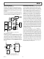
1
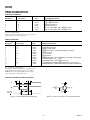
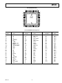
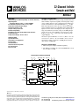
a 32-Channel Infinite Sample-and-Hold AD5533* FEATURES Infinite Sample-and-Hold Capability to ⴞ0.018% Accuracy High Integration: 32-Channel DAC in 12 mm ⴛ 12 mm CSPBGA Per Channel Acquisition Time of 16 s Max Adjustable Voltage Output Range Output Impedance 0.5 ⍀ Output Voltage Span 10 V Readback Capability DSP/Microcontroller Compatible Serial Interface Parallel Interface Temperature Range –40ⴗC to +85ⴗC GENERAL DESCRIPTION The AD5533 combines a 32-channel voltage translation function with an infinite output hold capability. An analog input voltage on the common input pin, VIN, is sampled and its digital representation transferred to a chosen DAC Register. VOUT for this DAC is then updated to reflect the new contents of the DAC register. Channel selection is accomplished via the parallel address inputs A0–A4 or via the serial input port. The output voltage range is determined by the offset voltage at the OFFS_IN pin and the gain of the output amplifier. It is restricted to a range from VSS + 2 V to VDD – 2 V because of the headroom of the output amplifier. The device is operated with AVCC = +5 V ± 5%, DVCC = +2.7 V to +5.25 V, VSS = –4.75 V to –16.5 V, and VDD = +8 V to +16.5 V and requires a stable 3 V reference on REF_IN as well as an offset voltage on OFFS_IN. APPLICATIONS Optical Networks Automatic Test Equipment Level Setting Instrumentation Industrial Control Systems Data Acquisition Low Cost I/O PRODUCT HIGHLIGHTS 1. Infinite Droopless Sample-and-Hold Capability. 2. The AD5533 is available in a 74-lead CSPBGA with a body size of 12 mm ⫻ 12 mm. FUNCTIONAL BLOCK DIAGRAM DVCC AVCC REF IN REF OUT OFFS IN VDD VSS VOUT 0 VIN ADC DAC TRACK / RESET BUSY DAC GND VOUT 31 AD5533 DAC AGND OFFS OUT DAC DGND SER / PAR INTERFACE CONTROL LOGIC SCLK D IN D OUT ADDRESS INPUT REGISTER SYNC/ CS A4 –A0 CAL WR OFFSET SEL *Protected by U.S. Patent No. 5,969,657. REV. A Information furnished by Analog Devices is believed to be accurate and reliable. However, no responsibility is assumed by Analog Devices for its use, nor for any infringements of patents or other rights of third parties that may result from its use. No license is granted by implication or otherwise under any patent or patent rights of Analog Devices. Trademarks and registered trademarks are the property of their respective companies. One Technology Way, P.O. Box 9106, Norwood, MA 02062-9106, U.S.A. Tel: 781/329-4700 www.analog.com Fax: 781/326-8703 © 2003 Analog Devices, Inc. All rights reserved. (VDD = +8 V to +16.5 V, VSS = –4.75 V to –16.5 V; AVCC = +4.75 V to +5.25 V; DVCC = 2.7 V AD5533–SPECIFICATIONS to 5.25 V; AGND = DGND = DAC_GND = 0 V; REF_IN = 3 V; Output Range from V + 2 V to V – 2 V. All outputs unloaded. All specifications T to T , unless otherwise noted.) SS DD Parameter1 MIN MAX A Version2 Unit Conditions/Comments ± 0.018 ± 0.006 3.46/3.6 ± 50 % max % typ min/max mV max Input Range 100 mV to 2.96 V. After Gain and Offset Adjustment. 3.52 typ. 0–3 70 V mV max Input Upper Dead Band 40 mV max Input Current 1 µA max Nominal Input Range. 50 mV typ. Referred to VIN. See Figure 5. 12 mV typ. Referred to VIN. See Figure 5. 100 nA typ. VIN Being Acquired on One Channel. Input Capacitance3 20 pF typ 1 0/4 µA max V min/max 3.0 2.85/3.15 1 V V min/max µA max 3 280 60 V typ kΩ typ ppm/°C typ 10 0.5 VSS + 2 /VDD – 2 5 500 7 –70 –70 250 ppm/°C typ Ω typ V min/max kΩ min pF max mA typ dB typ dB typ µV max 10 1.3 50 to REF_IN – 12 10 100 ppm/°C typ kΩ typ mV typ µA max pF max ± 10 0.8 0.4 2.4 2.0 200 10 µA max V max V max V min V min mV typ pF max 5 µA typ. DVCC = 5 V ± DVCC = 3 V ± DVCC = 5 V ± DVCC = 3 V ± 0.4 4.0 0.4 2.4 ±1 15 V max V min V max V min µA max pF typ DVCC = 5 V. Sinking 200 µA. DVCC = 5 V. Sourcing 200 µA. DVCC = 3 V. Sinking 200 µA. DVCC = 3 V. Sourcing 200 µA. DOUT Only. DOUT Only. ANALOG CHANNEL VIN to VOUT Nonlinearity Gain Offset Error ANALOG INPUT (VIN) Input Voltage Range Input Lower Dead Band ANALOG INPUT (OFFS_IN) Input Current Input Voltage Range VOLTAGE REFERENCE REF_IN Nominal Input Voltage Input Voltage Range3 Input Current REF_OUT Output Voltage Output Impedance3 Reference Temperature Coefficient 3 ANALOG OUTPUTS (VOUT 0–31) Output Temperature Coefficient 3, 4 DC Output Impedance Output Range Resistive Load3, 5 Capacitive Load3, 5 Short-Circuit Current3 DC Power Supply Rejection Ratio 3 DC Crosstalk3 ANALOG OUTPUT (OFFS_OUT) Output Temperature Coefficient 3, 4 DC Output Impedance3 Output Range Output Current Capacitive Load DIGITAL INPUTS3 Input Current Input Low Voltage Input High Voltage Input Hysteresis (SCLK and CS Only) Input Capacitance DIGITAL OUTPUTS (BUSY, DOUT)3 Output Low Voltage Output High Voltage Output Low Voltage Output High Voltage High Impedance Leakage Current High Impedance Output Capacitance –2– 100 nA typ. Output Range Restricted from VSS + 2 V to VDD – 2 V. <1 nA typ. VDD = +15 V ± 5%. VSS = –15 V ± 5%. Source Current. 5%. 10%. 5%. 10%. REV. A AD5533 Parameter1 POWER REQUIREMENTS Power Supply Voltages VDD VSS AVCC DVCC Power Supply Currents6 IDD ISS AICC DICC Power Dissipation6 A Version2 Unit 8/16.5 –4.75/–16.5 4.75/5.25 2.7/5.25 V min/max V min/max V min/max V min/max 15 15 33 1.5 280 mA max mA max mA max mA max mW typ Conditions/Comments 10 mA typ. All Channels Full-Scale. 10 mA typ. All Channels Full-Scale. 26 mA typ. 1 mA typ. VDD = +10 V, VSS = –5 V. NOTES 1 See Terminology. 2 A Version: Industrial temperature range –40°C to +85°C; typical at +25°C. 3 Guaranteed by design and characterization, not production tested. 4 AD780 as reference for the AD5533. 5 Ensure that you do not exceed T J (max). See maximum ratings. 6 Outputs unloaded. Specifications subject to change without notice. (VDD = 8 V to 16.5 V, VSS = –4.75 V to –16.5 V; AVCC = 4.75 V to 5.25 V; DVCC = 2.7 V to 5.25 V; AGND = DGND = DAC_GND = 0 V; REF_IN = 3 V; Output Range from VSS + 2 V to VDD – 2 V. All outputs unloaded. All specifications TMIN to TMAX, unless otherwise noted.) AC CHARACTERISTICS Parameter A Version1 Unit Conditions/Comments Output Settling Time2 Acquisition Time OFFS_IN Settling Time2 Digital Feedthrough2 Output Noise Spectral Density @ 1 kHz2 AC Crosstalk2 3 16 10 0.2 400 5 µs max µs max µs max nV-s typ nV/(√Hz) typ nV-s typ 500 pF, 5 kΩ Load; 0 V–3 V Step NOTES 1 A Version: Industrial temperature range –40°C to +85°C; typical at 25°C. 2 Guaranteed by design and characterization, not production tested. Specifications subject to change without notice. REV. A –3– AD5533 TIMING CHARACTERISTICS PARALLEL INTERFACE Parameter1, 2 Limit at TMIN, TMAX (A Version) Unit Conditions/Comments t1 t2 t3 t4 t5 t6 0 0 50 50 20 7 ns min ns min ns min ns min ns min ns min CS to WR Setup Time CS to WR Hold Time CS Pulsewidth Low WR Pulsewidth Low A4–A0, CAL, OFFS_SEL to WR Setup Time A4–A0, CAL, OFFS_SEL to WR Hold Time NOTES 1 See Interface Timing Diagram. 2 Guaranteed by design and characterization, not production tested. Specifications subject to change without notice. SERIAL INTERFACE Parameter1, 2 Limit at TMIN, TMAX (A Version) Unit Conditions/Comments fCLKIN t1 t2 t3 t4 t5 t6 t7 t8 3 t9 3 t10 t114 20 20 20 15 50 10 5 5 20 60 400 7 MHz max ns min ns min ns min ns min ns min ns min ns min ns max ns max ns min ns min SCLK Frequency SCLK High Pulsewidth SCLK Low Pulsewidth SYNC Falling Edge to SCLK Falling Edge Setup Time SYNC Low Time DIN Setup Time DIN Hold Time SYNC Falling Edge to SCLK Rising Edge Setup Time for Read Back SCLK Rising Edge to DOUT Valid SCLK Falling Edge to DOUT High Impedance 10th SCLK Falling Edge to SYNC Falling Edge for Read Back SCLK Falling Edge to SYNC Falling Edge Setup Time for Read Back NOTES 1 See Serial Interface Timing Diagrams. 2 Guaranteed by design and characterization, not production tested. 3 These numbers are measured with the load circuit of Figure 2. 4 SYNC should be taken low while SCLK is low for read back. Specifications subject to change without notice. PARALLEL INTERFACE TIMING DIAGRAM t2 t1 CS t3 200A t4 TO OUTPUT PIN WR t5 t6 1.6V CL 50pF 200A A4–A0, CAL, OFFS SEL Figure 1. Parallel Write (ISHA Mode Only) IOL IOH Figure 2. Load Circuit for DOUT Timing Specifications –4– REV. A AD5533 SERIAL INTERFACE TIMING DIAGRAMS t1 SCLK 1 2 3 4 5 6 7 8 9 10 t2 t3 SYNC t4 t5 t6 DIN MSB LSB Figure 3. 10-Bit Write (ISHA Mode and Both Readback Modes) t1 t7 SCLK 1 10 2 t11 3 4 5 6 7 8 9 10 11 12 13 14 t2 SYNC t10 t4 t8 t9 DOUT MSB LSB Figure 4. 14-Bit Read (Both Readback Modes) REV. A –5– AD5533 Max Power Dissipation . . . . . . . . . . . . (150°C – TA)/θJA mW3 Max Continuous Load Current at TJ = 70°C, per Channel Group . . . . . . . . . . . . . . . . . . . . . . . 15.5 mA4 ABSOLUTE MAXIMUM RATINGS 1, 2 (TA = 25°C, unless otherwise noted) VDD to AGND . . . . . . . . . . . . . . . . . . . . . . . . –0.3 V to +17 V VSS to AGND . . . . . . . . . . . . . . . . . . . . . . . . +0.3 V to –17 V AVCC to AGND, DAC_GND . . . . . . . . . . . . . –0.3 V to +7 V DVCC to DGND . . . . . . . . . . . . . . . . . . . . . . . –0.3 V to +7 V Digital Inputs to DGND . . . . . . . . . . –0.3 V to DVCC + 0.3 V Digital Outputs to DGND . . . . . . . . . –0.3 V to DVCC + 0.3 V REF_IN to AGND, DAC_GND . . . . –0.3 V to AVCC + 0.3 V VIN to AGND, DAC_GND . . . . . . . . –0.3 V to AVCC + 0.3 V VOUT0–31 to AGND . . . . . . . . . . VSS – 0.3 V to VDD + 0.3 V OFFS_IN to AGND . . . . . . . . . . VSS – 0.3 V to VDD + 0.3 V OFFS_OUT to AGND . . . . AGND – 0.3 V to AVCC + 0.3 V AGND to DGND. . . . . . . . . . . . . . . . . . . . . –0.3 V to +0.3 V Operating Temperature Range Industrial . . . . . . . . . . . . . . . . . . . . . . . . . . –40°C to +85°C Storage Temperature Range . . . . . . . . . . . . –65°C to +150°C Junction Temperature (TJ max) . . . . . . . . . . . . . . . . . . 150°C 74-Lead CSPBGA Package, θJA Thermal Impedance . . 41°C/W Reflow Soldering Peak Temperature . . . . . . . . . . . . . . . . . . . . . . . . . . 220°C Time at Peak Temperature . . . . . . . . . . . . 10 sec to 40 sec NOTES 1 Stresses above those listed under Absolute Maximum Ratings may cause permanent damage to the device. This is a stress rating only; functional operation of the device at these or any other conditions above those listed in the operational sections of this specification is not implied. Exposure to absolute maximum rating conditions for extended periods may affect device reliability. 2 Transient currents of up to 100 mA will not cause SCR latch-up. 3 This limit includes load power. 4 This maximum allowed continuous load current is spread over eight channels and channels are grouped as follows: Group 1: Channels 3, 4, 5, 6, 7, 8, 9, 10 Group 2: Channels 14, 16, 18, 20. 21, 24, 25, 26 Group 3: Channels 15, 17, 19, 22, 23, 27, 28, 29 Group 4: Channels 0, 1, 2, 11, 12, 13, 30, 31 For higher junction temperatures derate as follows: TJ (°C) Max Continuous Load Current per Group (mA) 70 90 100 110 125 135 150 15.5 9.025 6.925 5.175 3.425 2.55 1.5 ORDERING GUIDE Model Function AD5533ABC-1 AD5533ABC-1REEL AD5533BBC-1* AD5532ABC-1* AD5532ABC-2* AD5532ABC-3* AD5532ABC-5* AD5532BBC-1* AD5532HS* EVAL-AD5532EB 32-Channel ISHA Only 32-Channel ISHA Only 32-Channel Precision ISHA Only 32 DACs, 32-Channel ISHA 32 DACs, 32-Channel ISHA 32 DACs, 32-Channel ISHA 32 DACs, 32-Channel ISHA 32 DACs, 32-Channel Precision ISHA 32-Channel High-Speed DAC AD5532/AD5533 Evaluation Board Output Impedance Output Voltage Span Package Description Package Option 0.5 Ω typ 0.5 Ω typ 0.5 Ω typ 0.5 Ω typ 0.5 Ω typ 500 Ω typ 1 kΩ typ 0.5 Ω typ 0.5 kΩ typ 10 V 10 V 10 V 10 V 20 V 10 V 10 V 10 V 5V 74-Lead CSPBGA 74-Lead CSPBGA 74-Lead CSPBGA 74-Lead CSPBGA 74-Lead CSPBGA 74-Lead CSPBGA 74-Lead CSPBGA 74-Lead CSPBGA 74-Lead CSPBGA BC-74 BC-74 BC-74 BC-74 BC-74 BC-74 BC-74 BC-74 BC-74 *Separate Data Sheet. CAUTION ESD (electrostatic discharge) sensitive device. Electrostatic charges as high as 4000 V readily accumulate on the human body and test equipment and can discharge without detection. Although the AD5533 features proprietary ESD protection circuitry, permanent damage may occur on devices subjected to high energy electrostatic discharges. Therefore, proper ESD precautions are recommended to avoid performance degradation or loss of functionality. –6– REV. A AD5533 PIN CONFIGURATION 1 2 3 4 5 6 7 8 9 10 11 A A B B C C D TOP VIEW D E AD5533 E F F G G H H J J K K L L 1 2 3 4 5 6 7 8 9 10 11 74-Lead CSPBGA Ball Configuration CSPBGA Number Ball Name CSPBGA Number Ball Name CSPBGA Number Ball Name A1 A2 A3 A4 A5 A6 A7 A8 A9 A10 A11 B1 B2 B3 B4 B5 B6 B7 B8 B9 B10 B11 C1 C2 C6 N/C* A4 A2 A0 CS/SYNC DVCC SCLK OFFSET_SEL BUSY TRACK/RESET N/C* VO16 N/C* A3 A1 WR DGND DIN CAL SER/PAR DOUT REF_IN VO18 DAC_GND1 N/C* C10 C11 D1 D2 D10 D11 E1 E2 E10 E11 F1 F2 F10 F11 G1 G2 G10 G11 H1 H2 H10 H11 J1 J2 J6 AVCC1 REF_OUT VO20 DAC_GND2 AVCC2 OFFS_OUT VO26 VO14 AGND1 OFFS_IN VO25 VO21 AGND2 VO6 VO24 VO8 VO5 VO3 VO23 VIN VO4 VO7 VO22 VO19 VSS2 J10 J11 K1 K2 K3 K4 K5 K6 K7 K8 K9 K10 K11 L1 L2 L3 L4 L5 L6 L7 L8 L9 L10 L11 VO9 VO11 VO17 VO15 VO27 VSS3 VSS1 VSS4 VDD2 VO2 VO10 VO13 VO12 N/C* VO28 VO29 VO30 VDD3 VDD1 VDD4 VO31 VO0 VO1 N/C* *N/C = unconnected REV. A –7– AD5533 PIN FUNCTION DESCRIPTIONS Pin Function AGND(1–2) AVCC (1–2) VDD (1–4) VSS (1–4) DGND DVCC DAC_GND(1–2) REF_IN REF_OUT VOUT (0–31) VIN A4–A11, A02 CAL1 CS/SYNC Analog GND Pins Analog Supply Pins. Voltage range from 4.75 V to 5.25 V. VDD Supply Pins. Voltage range from 8 V to 16.5 V. VSS Supply Pins. Voltage range from –4.75 V to –16.5 V. Digital GND Pins Digital Supply Pins. Voltage range from 2.7 V to 5.25 V. Reference GND Supply for All the DACs Reference Voltage for Channels 0–31 Reference Output Voltage Analog Output Voltages from the 32 Channels Analog Input Voltage Parallel Interface: 5-Address Pins for 32 Channels. A4 = MSB of Channel Address. A0 = LSB. Parallel Interface: Control input that allows all 32 channels to acquire VIN simultaneously. This pin is both the Active Low Chip Select Pin for the parallel interface and the Frame Synchronization Pin for the serial interface. Parallel Interface: Write Pin. Active low. This is used in conjunction with the CS Pin to address the device using the parallel interface. Parallel Interface: Offset Select Pin. Active high. This is used to select the offset channel. Serial Clock Input for Serial Interface. This operates at clock speeds up to 20 MHz. Data Input for Serial Interface. Data must be valid on the falling edge of SCLK. Output from the DAC Registers for read back. Data is clocked out on the rising edge of SCLK and is valid on the falling edge of SCLK. This pin allows the user to select whether the serial or parallel interface will be used. If the pin is tied low, the parallel interface will be used. If it is tied high, the serial interface will be used. Offset Input. The user can supply a voltage here to offset the output span. OFFS_OUT can also be tied to this pin if the user wants to drive this pin with the offset channel. Offset Output. This is the acquired offset voltage that can be tied to the OFFS_IN Pin to offset the span. This output tells the user when the input voltage is being acquired. It goes low during acquisition and returns high when the acquisition operation is complete. If this input is held high, VIN is acquired once the channel is addressed. While it is held low, the input to the gain/offset stage is switched directly to VIN. The addressed channel begins to acquire VIN on the rising edge of TRACK. See TRACK Function section for further information. This input can also be used as a means of resetting the complete device to its power-on-reset conditions. This is achieved by applying a low-going pulse of between 90 ns and 200 ns to this pin. See section on RESET Function for further details. WR1 OFFSET_SEL1 SCLK2 DIN2 DOUT SER/PAR1 OFFS_IN OFFS_OUT BUSY TRACK/RESET2 NOTES 1 Internal pull-down devices on these logic inputs. Therefore, they can be left floating and will default to a logic low condition. 2 Internal pull-up devices on these logic inputs. Therefore, they can be left floating and will default to a logic high condition. –8– REV. A AD5533 TERMINOLOGY VIN to VOUT Nonlinearity DC Crosstalk This is the dc change in the output level of one channel in response to a full-scale change in the output of all other channels. It is expressed in µV. This is a measure of the maximum deviation from a straight line passing through the endpoints of the VIN versus VOUT transfer function. It is expressed as a percentage of the full-scale span. Output Settling Time This is the time taken from when BUSY goes high to when the output has settled to ± 0.018%. Offset Error This is a measure of the output error when VIN = 70 mV. Ideally, with VIN = 70 mV: ( Acquisition Time ) VOUT = (Gain × 70) – (Gain – 1) × VOFFS _ IN mV This is the time taken for the VIN input to be acquired. It is the length of time that BUSY stays low. Offset error is a measure of the difference between VOUT (actual) and VOUT (ideal). It is expressed in mV and can be positive or negative. See Figure 5. OFFS_IN Settling Time This is the time taken from a 0 V–3 V step change in input voltage on OFFS_IN until the output has settled to within ± 0.39%. Gain Error Digital Feedthrough This is a measure of the span error of the analog channel. It is the deviation in slope of the transfer function. See Figure 5. It is calculated as: This is a measure of the impulse injected into the analog outputs from the digital control inputs when the part is not being written to, i.e., CS/SYNC is high. It is specified in nV-s and is measured with a worst-case change on the Digital Input Pins, e.g., from all 0s to all 1s and vice versa. Gain Error = Actual Full-Scale Output – Ideal Full-Scale Output – Offset Error where: Ideal Full-Scale Output = Ideal Gain × 2.96 – ( Ideal Gain – 1) × VOFFS _ IN Ideal Gain = 3.52 ( Output Noise Spectral Density This is a measure of internally generated random noise. Random noise is characterized as a spectral density (voltage per root Hertz). It is measured by loading all DACs to midscale and measuring noise at the output. It is measured in nV/(√Hz). ) Output Temperature Coefficient AC Crosstalk This is a measure of the change in analog output with changes in temperature. It is expressed in ppm/°C. This is the area of the glitch that occurs on the output of one channel while another channel is acquiring. It is expressed in nV-s. DC Power Supply Rejection Ratio DC power supply rejection ratio (PSRR) is a measure of the change in the analog output for a change in the supply voltage (VDD and VSS). It is expressed in dBs. VDD and VSS are varied ±5%. VOUT GAIN ERROR + OFFSET ERROR IDEAL TRANSFER FUNCTION ACTUAL TRANSFER FUNCTION OFFSET ERROR 0V 70mV 2.96 LOWER DEAD BAND Figure 5. ISHA Transfer Function REV. A 3V UPPER DEAD BAND –9– VIN AD5533–Typical Performance Characteristics 20 0.0016 OFFSET ERROR – mV VOUT ERROR – V 0.0012 0.0008 0.0004 0.0000 –0.0004 –0.0008 –0.0012 3.535 3.56 15 TA = 25ⴗC VREFIN = 3V VIN = 1V 3.54 GAIN 3.530 10 3.52 OFFSET ERROR VOUT – V TA = 25ⴗC VREFIN = 3V VOFFS_IN = 0V 0.0020 GAIN 0.0024 3.525 5 3.50 –0.0016 –0.0020 –0.0024 0.1 0 –40 2.96 VIN – V TPC 1. V IN to V OUT Accuracy after Offset and Gain Adjustment 0 40 TEMPERATURE – ⴗC 80 3.48 TPC 2. Offset Error and Gain vs. Temperature 3.520 6 4 2 –2 –4 0 SINK/SOURCE CURRENT – mA –6 TPC 3. VOUT Source and Sink Capability 70k 63791 60k 5V 100 50k VOUT TA = 25ⴗC VREFIN = 3V VIN = 0 1.5V 10 FREQUENCY BUSY 90 TA = 25ⴗC VREFIN = 3V VIN = 1.5V VOFFS_IN = 0V 40k 30k 20k 0% 1V 2s 10k 0 TPC 4. Acquisition Time and Output Settling Time 1545 200 5.2670 5.2676 VOUT – V 5.2682 TPC 5. ISHA Mode Repeatability (64 K Acquisitions) –10– REV. A AD5533 FUNCTIONAL DESCRIPTION ADDRESSED CHANNEL The AD5533 can be thought of as consisting of an ADC and 32 DACs in a single package. The input voltage VIN is sampled and converted into a digital word. The digital result is loaded into one of the DAC Registers and is converted (with gain and offset) into an analog output voltage (VOUT0–VOUT31). Since the channel output voltage is effectively the output of a DAC, there is no droop associated with it. As long as power to the device is maintained, the output voltage will remain constant until this channel is addressed again. To update a single channel’s output voltage, the required new voltage level is set up on the Common Input Pin, VIN. The desired channel is then addressed via the Parallel Port or the Serial Port. When the channel address has been loaded, provided TRACK is high, the circuit begins to acquire the correct code to load to the DAC in order that the DAC output matches the voltage on VIN. The BUSY Pin goes low and remains so until the acquisition is complete. The noninverting input to the output buffer is tied to VIN during the acquisition period to avoid spurious outputs, while the DAC acquires the correct code. The acquisition is completed in 16 µs max. The BUSY Pin goes high and the updated DAC output assumes control of the output voltage. The output voltage of the DAC is connected to the noninverting input of the output buffer. Since the internal DACs are offset by 70 mV (max) from GND, the minimum VIN in ISHA Mode is 70 mV. The maximum VIN is 2.96 V due to the upper dead band of 40 mV (max). On power-on, all the DACs, including the offset channel, are loaded with zeros. Each of the 33 DACs is offset internally by 50 mV (typ) from GND so the outputs VOUT0 to VOUT31 are 50 mV (typ) on power-on if the OFFS_IN Pin is driven directly by the on-board offset channel (OFFS_OUT), i.e.: If OFFS_IN = OFFS_OUT = 50 mV = > VOUT = (Gain × VDAC) – (Gain – 1) × VOFFS_IN = 50 mV. Analog Input The equivalent analog input circuit is shown in Figure 6. The Capacitor C1 is typically 20 pF and can be attributed to the pin capacitance and 32 off-channels. When a channel is selected, an extra 7.5 pF (typ) is switched in. This Capacitor C2 is charged to the previously acquired voltage on that particular channel so it must charge/discharge to the new level. It is essential that the external source can charge/discharge this additional capacitance within 1 µs–2 µs of channel selection so that VIN can be acquired accurately. For this reason a low impedance source is recommended. VIN C2 7.5pF C1 20pF Figure 6. Analog Input Circuit Large source impedances will significantly affect the performance of the ADC. This may necessitate the use of an input buffer amplifier. Output Buffer Stage—Gain and Offset The function of the output buffer stage is to translate the 50 mV–3 V output of the DAC to a wider range. This is done by gaining up the DAC output by 3.52 and offsetting the voltage by the voltage on the OFFS_IN Pin. VOUT = 3.52 × VDAC − 2.52 × VOFFS _ IN VDAC is the output of the DAC. VOFFS_IN is the voltage at the OFFS_IN Pin. Table I shows how the output range on VOUT relates to the offset voltage supplied by the user. Table I. Sample Output Voltage Ranges VOFFS_IN (V) VDAC (V) VOUT (V) 0 1 2.130 0.05 to 3 0.05 to 3 0.05 to 3 0.176 to 10.56 –2.34 to +8.06 –5.192 to +5.192 VOUT is limited only by the headroom of the output amplifiers, VOUT must be within the maximum ratings. Offset Voltage Channel The offset voltage can be externally supplied by the user at OFFS_IN or it can be supplied by an additional offset voltage channel on the device itself. The required offset voltage is set up on VIN and acquired by the offset DAC. This offset channel’s DAC output is directly connected to OFFS_OUT. By connecting OFFS_OUT to OFFS_IN this offset voltage can be used as the offset voltage for the 32-output amplifiers. It is important to choose the offset so that VOUT is within maximum ratings. PIN DRIVER CONTROLLER DAC VIN OUTPUT STAGE ACQUISITION CIRCUIT BUSY VOUT1 DEVICE UNDER TEST AD5533 TRACK THRESHOLD VOLTAGE ONLY ONE CHANNEL SHOWN FOR SIMPLICITY Figure 7. Typical ATE Circuit Using TRACK Input REV. A –11– AD5533 Reset Function The reset function on the AD5533 can be used to reset all nodes on this device to their power-on-reset condition. This is implemented by applying a low-going pulse of between 90 ns and 200 ns to the TRACK/RESET Pin on the device. If the applied pulse is less than 90 ns, it is assumed to be a glitch and no operation takes place. If the applied pulse is wider than 200 ns, this pin adopts its TRACK function on the selected channel, VIN is switched to the output buffer, and an acquisition on the channel will not occur until a rising edge of TRACK. TRACK Function Normally in the ISHA Mode of operation, TRACK is held high and the channel begins to acquire when it is addressed. However, if TRACK is low when the channel is addressed, VIN is switched to the output buffer and an acquisition on the channel will not occur until a rising edge of TRACK. At this stage, the BUSY Pin will go low until the acquisition is complete, at which point the DAC assumes control of the voltage to the output buffer and VIN is free to change again without affecting this output value. This is useful in an application where the user wants to ramp up VIN until VOUT reaches a particular level (Figure 7). VIN does not need to be acquired continuously while it is ramping up. TRACK can be kept low and only when VOUT has reached its desired voltage is TRACK brought high. At this stage, the acquisition of VIN begins. In the example shown, a desired voltage is required on the output of the pin driver. This voltage is represented by one input to a comparator. The µC/µP ramps up the input voltage on VIN through a DAC. TRACK is kept low while the voltage on VIN ramps up so that VIN is not continually acquired. When the desired voltage is reached on the output of the pin driver, the comparator output switches. The µC/µP then knows what code is required to be input in order to obtain the desired voltage at the DUT. The TRACK input is now brought high and the part begins to acquire VIN. BUSY goes low until VIN has been acquired. When BUSY goes high, the output buffer is switched from VIN to the output of the DAC. 1. ISHA Mode In this standard mode, a channel is addressed and that channel acquires the voltage on VIN. This mode requires a 10-bit write to address the relevant channel (VOUT0–VOUT31, offset channel or all channels). MSB is written first. 2. Acquire and Readback Mode This mode allows the user to acquire VIN and read back the data in a particular DAC Register. The relevant channel is addressed (10-bit write, MSB first) and VIN is acquired in 16 µs (max). Following the acquisition, after the next falling edge of SYNC the data in the relevant DAC Register is clocked out onto the DOUT line in a 14-bit serial format. During read back DIN is ignored. The full acquisition time must elapse before the DAC register data can be clocked out. 3. Readback Mode Again, this is a Readback Mode but no acquisition is performed. The relevant channel is addressed (10-bit write, MSB first) and on the next falling edge of SYNC, the data in the relevant DAC Register is clocked out onto the DOUT line in a 14-bit serial format. The user must allow 400 ns (min) between the last SCLK falling edge in the 10-bit write and the falling edge of SYNC in the 14-bit read back. The serial write and read words can be seen in Figure 8. This feature allows the user to read back the DAC Register code of any of the channels. Read back is useful if the system has been calibrated and the user wants to know what code in the DAC corresponds to a desired voltage on VOUT. INTERFACES Serial Interface The SER/PAR Pin is tied high to enable the serial interface and to disable the parallel interface. The serial interface is controlled by the four pins that follow. MODES OF OPERATION The AD5533 can be used in three different modes. These modes are set by two mode bits, the first two bits in the serial word. The 01 option (DAC Mode) is not available for the AD5533. To avail of this mode, refer to the AD5532 data sheet. If you attempt to set up DAC Mode, the AD5533 will enter a Test Mode and a 24-clock write will be necessary to clear this. SYNC, DIN, SCLK Standard 3-wire Interface Pins. The SYNC Pin is shared with the CS function of the parallel interface. DOUT Data Out Pin for reading back the contents of the DAC Registers. The data is clocked out on the rising edge of SCLK and is valid on the falling edge of SCLK. CAL Bit When this is high, all 32 channels acquire VIN simultaneously. The acquisition time is then 45 µs (typ) and accuracy may be reduced. OFFSET_SEL Bit Table II. Modes of Operation If this bit is set high, the offset channel is selected and Bits A4–A0 are ignored. Mode Bit 1 Mode Bit 2 Operating Mode 0 0 1 1 0 1 0 1 ISHA Mode DAC Mode (Not Available) Acquire and Read Back Read Back Test Bit This must be set low for correct operation of the part. A4–A0 Used to address any one of the 32 channels (A4 = MSB of address, A0 = LSB). DB13–DB0 These are used in both Readback Modes to read a 14-bit word from the addressed DAC Register. –12– REV. A AD5533 MSB LSB 0 0 MODE BIT 1 CAL 0 OFFSET SEL MODE BIT 2 A4 –A0 TEST BIT MODE BITS a. 10-Bit Input Serial Write Word (ISHA Mode) LSB MSB 1 0 CAL OFFSET SEL MSB A4 –A0 0 LSB DB1 3 –DB0 TEST BIT MODE BITS 14-BIT DATA READ FROM PART AFTER NEXT FALLING EDGE OF SYNC (DB13 = MSB OF DAC WORD) 10-BIT SERIAL WORD WRITTEN TO PART b. Input Serial Interface (Acquire and Readback Mode) LSB MSB 1 1 0 OFFSET SEL 0 MSB A4 –A0 LSB DB1 3 –DB0 TEST BIT MODE BITS 14-BIT DATA READ FROM PART AFTER NEXT FALLING EDGE OF SYNC (DB13 = MSB OF DAC WORD) 10-BIT SERIAL WORD WRITTEN TO PART c. Input Serial Interface (Readback Mode) Figure 8. Serial Interface Formats The serial interface is designed to allow easy interfacing to most microcontrollers and DSPs, e.g., PIC16C, PIC17C, QSPI™, SPI®, DSP56000, TMS320, and ADSP-21xx, without the need for any glue logic. When interfacing to the 8051, the SCLK must be inverted. The Microprocessor Interfacing section explains how to interface to some popular DSPs and microcontrollers. Parallel Interface The SER/PAR Bit must be tied low to enable the parallel interface and disable the serial interface. The parallel interface is controlled by nine pins. Figures 3 and 4 show the timing diagram for a serial read and write to the AD5533. The serial interface works with both a continuous and a noncontinuous serial clock. The first falling edge of SYNC resets a counter that counts the number of serial clocks to ensure the correct number of bits are shifted in and out of the Serial Shift Registers. Any further edges on SYNC are ignored until the correct number of bits are shifted in or out. Once the correct number of bits have been shifted in or out, the SCLK is ignored. In order for another serial transfer to take place, the counter must be reset by the falling edge of SYNC. In read back, the first rising SCLK edge after the falling edge of SYNC causes DOUT to leave its high impedance state and data is clocked out onto the DOUT line and also on subsequent SCLK rising edges. The DOUT Pin goes back into a high impedance state on the falling edge of the 14th SCLK. Data on the DIN line is latched in on the first SCLK falling edge after the falling edge of the SYNC signal and on subsequent SCLK falling edges. The serial interface will not shift data in or out until it receives the falling edge of the SYNC signal. REV. A CS Active Low Package Select Pin. This pin is shared with the SYNC function for the serial interface. WR Active Low Write Pin. The values on the Address Pins are latched on a rising edge of WR. A4–A0 Five Address Pins (A4 = MSB of address, A0 = LSB). These are used to address the relevant channel (out of a possible 32). OFFSET_SEL Offset Select Pin. This has the same function as the OFFSET_SEL Bit in the serial interface. When it is high, the offset channel is addressed and the address on A4–A0 is ignored. CAL Same functionality as the CAL Bit in the serial interface. When this pin is high, all 32 channels acquire VIN simultaneously. –13– AD5533 SPDR Register. PC7 must be pulled low to start a transfer. It is taken high and pulled low again before any further read/write cycles can take place. A connection diagram is shown in Figure 10. MICROPROCESSOR INTERFACING AD5533 to ADSP-21xx Interface The ADSP-21xx family of DSPs are easily interfaced to the AD5533 without the need for extra logic. AD5533* A data transfer is initiated by writing a word to the Tx Register after the SPORT has been enabled. In a write sequence, data is clocked out on each rising edge of the DSP’s serial clock and clocked into the AD5533 on the falling edge of its SCLK. In read back, 16 bits of data are clocked out of the AD5533 on each rising edge of SCLK and clocked into the DSP on the rising edge of SCLK. DIN is ignored. The valid 14 bits of data will be centered in the 16-bit Rx Register when using this configuration. The SPORT Control Register should be set up as follows: TFSW INVRFS DTYPE ISCLK TFSR IRFS ITFS SLEN SLEN MC68HC11* D OUT MISO SYNC PC7 SCLK SCK D IN *ADDITIONAL PINS OMITTED FOR CLARITY Figure 10. AD5533 to MC68HC11 Interface AD5533 to PIC16C6x/PIC16C7x The PIC16C6x Synchronous Serial Port (SSP) is configured as an SPI Master with the Clock Polarity Bit = 0. This is done by writing to the Synchronous Serial Port Control Register (SSPCON). See PIC16/PIC17 Microcontroller User Manual. In this example, I/O port RA1 is being used to pulse SYNC and enable the serial port of the AD5533. This microcontroller transfers only eight bits of data during each serial transfer operation; therefore, two consecutive read/write operations are needed for a 10-bit write and a 14-bit read back. Figure 11 shows the connection diagram. = RFSW = 1, Alternate Framing = INVTFS = 1, Active Low Frame Signal = 00, Right Justify Data = 1, Internal Serial Clock = RFSR = 1, Frame Every Word = 0, External Framing Signal = 1, Internal Framing Signal = 1001, 10-Bit Data-Words (ISHA Mode Write) = 1111, 16-Bit Data-Words (Readback Mode) Figure 9 shows the connection diagram. PIC16C6x/7x* AD5533* AD5533* D OUT DR SYNC TFS MOSI ADSP-2101/ ADSP-2103* SCLK SCK/RC3 D OUT SDO/RC5 D IN SYNC SDI/RC4 RA1 RFS D IN SCLK *ADDITIONAL PINS OMITTED FOR CLARITY DT Figure 11. AD5533 to PIC16C6x/7x Interface SCLK AD5533 to 8051 *ADDITIONAL PINS OMITTED FOR CLARITY Figure 9. AD5533 to ADSP-2101/ADSP-2103 Interface AD5533 to MC68HC11 The Serial Peripheral Interface (SPI) on the MC68HC11 is configured for Master Mode (MSTR) = 1, Clock Polarity Bit (CPOL) = 0, and the Clock Phase Bit (CPHA) = 1. The SPI is configured by writing to the SPI Control Register (SPCR)—see 68HC11 User Manual. SCK of the 68HC11 drives the SCLK of the AD5533, the MOSI output drives the serial data line (DIN) of the AD5533, and the MISO input is driven from DOUT. The SYNC signal is derived from a port line (PC7). When data is being transmitted to the AD5533, the SYNC line is taken low (PC7). Data appearing on the MOSI output is valid on the falling edge of SCK. Serial data from the 68HC11 is transmitted in 8-bit bytes with only eight falling clock edges occurring in the transmit cycle. Data is transmitted MSB first. To transmit 10 data bits in ISHA Mode, it is important to left-justify the data in the The AD5533 requires a clock synchronized to the serial data. The 8051 serial interface must therefore be operated in Mode 0. In this mode, serial data enters and exits through RxD and a shift clock is output on TxD. Figure 12 shows how the 8051 is connected to the AD5533. Because the AD5533 shifts data out on the rising edge of the shift clock and latches data in on the falling edge, the shift clock must be inverted. The AD5533 requires its data with the MSB first. Since the 8051 outputs the LSB first, the transmit routine must take this into account. AD5533* 8051* SCLK TxD D OUT RxD D IN SYNC P1.1 *ADDITIONAL PINS OMITTED FOR CLARITY Figure 12. AD5533 to 8051 Interface –14– REV. A AD5533 APPLICATION CIRCUITS AD5533 in a Typical ATE System POWER SUPPLY DECOUPLING The AD5533 infinite sample-and-hold is ideally suited for use in automatic test equipment. Several ISHAs are required to control pin drivers, comparators, active loads, and signal timing. Traditionally, sample-and-hold devices with droop were used in this application. These required refreshing to prevent the voltage from drifting. The AD5533 has several advantages: no refreshing is required, there is no droop, pedestal error is eliminated, and there is no need for extra filtering to remove glitches. Overall, a higher level of integration is achieved in a smaller area, see Figure 13. PARAMETRIC MEASUREMENT SYSTEM BUS UNIT ISHA ISHA ACTIVE LOAD ISHA STORED DATA AND INHIBIT PATTERN DRIVER ISHA FORMATTER DUT ISHA PERIOD GENERATION AND DELAY TIMING ISHA COMPARE REGISTER ISHA COMPARATOR ISHAs SYSTEM BUS Figure 13. AD5533 in an ATE System Typical Application Circuit The AD5533 can be used to set up voltage levels on 32 channels as shown in the circuit below. An AD780 provides the 3 V reference for the AD5533 and for the AD5541 16-bit DAC. A simple 3-wire interface is used to write to the AD5541. Because the AD5541 has an output resistance of 6.25 kΩ (typ), the time taken to charge/discharge the capacitance at the VIN Pin is significant. Hence an AD820 is used to buffer the DAC output. Note that it is important to minimize noise on VIN and REFIN when laying out this circuit. AVCC In any circuit where accuracy is important, careful consideration of the power supply and ground return layout helps to ensure the rated performance. The printed circuit board on which the AD5533 is mounted should be designed so that the analog and digital sections are separated and confined to certain areas of the board. If the AD5533 is in a system where multiple devices require an AGND-to-DGND connection, the connection should be made at one point only. The star ground point should be established as close as possible to the device. For supplies with multiple pins (VSS, VDD, and AVCC), it is recommended to tie those pins together. The AD5533 should have ample supply bypassing of 10 µF in parallel with 0.1 µF on each supply located as close to the package as possible, ideally right up against the device. The 10 µF capacitors are the tantalum bead type. The 0.1 µF capacitor should have low effective series resistance (ESR) and effective series inductance (ESI), like the common ceramic types that provide a low impedance path to ground at high frequencies, to handle transient currents due to internal logic switching. The power supply lines of the AD5533 should use as large a trace as possible to provide low impedance paths and reduce the effects of glitches on the power supply line. Fast switching signals, such as clocks, should be shielded with digital ground to avoid radiating noise to other parts of the board and should never be run near the reference inputs. A ground line routed between the DIN and SCLK lines will help reduce crosstalk between them (not required on a multilayer board as there will be a separate ground plane but separating the lines will help). Note it is essential to minimize noise on VIN and REFIN lines. Particularly for optimum ISHA performance, the VIN line must be kept noise-free. Depending on the noise performance of the board, a noise filtering capacitor may be required on the VIN line. If this capacitor is necessary, then for optimum throughput it may be necessary to buffer the source which is driving VIN. Avoid crossover of digital and analog signals. Traces on opposite sides of the board should run at right angles to each other. This reduces the effects of feedthrough through the board. A microstrip technique is by far the best but not always possible with a double-sided board. In this technique, the component side of the board is dedicated to ground plane while signal traces are placed on the solder side. As is the case for all thin packages, care must be taken to avoid flexing the package and to avoid a point load on the surface of the package during the assembly process. AVCC DVCC VSS VDD CS DIN SCLK AD5541* AD820 VIN VOUT 0–31 AD5533* REF OFFS_IN OFFS_OUT REFIN AD780* VOUT SCLK DIN SYNC *ADDITIONAL PINS OMITTED FOR CLARITY Figure 14. Typical Application Circuit REV. A –15– AD5533 OUTLINE DIMENSIONS 74-Lead Chip Scale Ball Grid Array [CSPBGA] (BC-74) A1 CORNER INDEX AREA 12.00 BSC SQ 11 10 9 8 7 6 5 4 3 2 1 A1 TOP VIEW C00940–0–7/03(A) Dimensions shown in millimeters 1.00 BSC BOT TOM VIEW A B C D E F G H J K L 10.00 BSC SQ 1.00 BSC 1.70 MAX DETAIL A DETAIL A 0.30 MIN 0.20 MAX COPLANARITY 0.70 SEATING 0.60 PLANE 0.50 BALL DIAMETER COMPLIANT TO JEDEC STANDARDS MO-192ABD-1 Revision History Location Page 7/03—Data Sheet changed from REV. 0 to REV. A. Term SHA changed to ISHA . . . . . . . . . . . . . . . . . . . . . . . . . . . . . . . . . . . . . . . . . . . . . . . . . . . . . . . . . . . . . . . . . . . . . . . . . . . Global Term LFBGA updated to CSPBGA . . . . . . . . . . . . . . . . . . . . . . . . . . . . . . . . . . . . . . . . . . . . . . . . . . . . . . . . . . . . . . . . . . . . . Global Changes to APPLICATIONS . . . . . . . . . . . . . . . . . . . . . . . . . . . . . . . . . . . . . . . . . . . . . . . . . . . . . . . . . . . . . . . . . . . . . . . . . . . . . . 1 Changes to SPECIFICATIONS . . . . . . . . . . . . . . . . . . . . . . . . . . . . . . . . . . . . . . . . . . . . . . . . . . . . . . . . . . . . . . . . . . . . . . . . . . . . 2 Changes to TIMING CHARACTERISTICS . . . . . . . . . . . . . . . . . . . . . . . . . . . . . . . . . . . . . . . . . . . . . . . . . . . . . . . . . . . . . . . . . . 4 Changes to ABSOLUTE MAXIMUM RATINGS . . . . . . . . . . . . . . . . . . . . . . . . . . . . . . . . . . . . . . . . . . . . . . . . . . . . . . . . . . . . . . 6 Changes to ORDERING GUIDE . . . . . . . . . . . . . . . . . . . . . . . . . . . . . . . . . . . . . . . . . . . . . . . . . . . . . . . . . . . . . . . . . . . . . . . . . . . 6 Edits to PIN FUNCTION DESCRIPTION . . . . . . . . . . . . . . . . . . . . . . . . . . . . . . . . . . . . . . . . . . . . . . . . . . . . . . . . . . . . . . . . . . . 8 Changes to TERMINOLOGY . . . . . . . . . . . . . . . . . . . . . . . . . . . . . . . . . . . . . . . . . . . . . . . . . . . . . . . . . . . . . . . . . . . . . . . . . . . . . 9 Changes to FUNCTIONAL DESCRIPTION . . . . . . . . . . . . . . . . . . . . . . . . . . . . . . . . . . . . . . . . . . . . . . . . . . . . . . . . . . . . . . . . 11 Changes to Table I . . . . . . . . . . . . . . . . . . . . . . . . . . . . . . . . . . . . . . . . . . . . . . . . . . . . . . . . . . . . . . . . . . . . . . . . . . . . . . . . . . . . . 11 Changes to APPLICATION CIRCUITS . . . . . . . . . . . . . . . . . . . . . . . . . . . . . . . . . . . . . . . . . . . . . . . . . . . . . . . . . . . . . . . . . . . . 15 Updated OUTLINE DIMENSIONS . . . . . . . . . . . . . . . . . . . . . . . . . . . . . . . . . . . . . . . . . . . . . . . . . . . . . . . . . . . . . . . . . . . . . . . 16 –16– REV. A