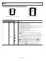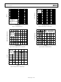
1
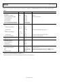
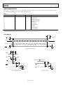
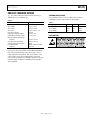
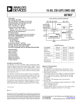
Quad, 12-Bit, Serial Input,
Unipolar/Bipolar, Voltage Output DAC
AD5726
Data Sheet
the VREFN input is set to 0 V and the VREFP input is set to a positive
voltage. A similar configuration with VREFP at 0 V and VREFN at a
negative voltage provides a unipolar negative output range.
FEATURES
+5 V to ±15 V operation
Unipolar or bipolar operation
±1 LSB maximum INL error, ±1 LSB maximum DNL error
Guaranteed monotonic over temperature
Double-buffered inputs
Asynchronous CLR to zero scale/midscale
Operating temperature range: −40°C to +125°C
iCMOS process technology
Bipolar outputs are configured by connecting both VREFP and
VREFN to nonzero voltages. This method of setting output voltage
ranges has advantages over the bipolar offsetting methods
because it is not dependent on internal and external resistors
with different temperature coefficients.
The AD5726 uses a serial interface that operates at clock rates up to
30 MHz and is compatible with DSP and microcontroller interface
standards. The asynchronous CLR function clears all DAC
registers to a user-selectable zero-scale or midscale output.
APPLICATIONS
Industrial automation
Closed-loop servo control, process control
Automotive test and measurement
Programmable logic controllers
The AD5726 is available in 16-lead SSOP, 20-lead SSOP, and
16-lead SOIC packages. It can be operated from a wide variety
of supply and reference voltages with supplies ranging from
single +5 V to ±15 V, and references ranging from +2.5 V to
±10 V. Power dissipation is less than 240 mW with ±15 V
supplies and only 30 mW with a +5 V supply. Operation is
specified over the temperature range of −40°C to +125°C.
GENERAL DESCRIPTION
The AD5726 is a quad, 12-bit, serial input, voltage output
digital-to-analog converter (DAC) fabricated on Analog
Devices, Inc., iCMOS® process technology1 that offers
guaranteed monotonicity and integral nonlinearity (INL)
of ±1 LSB maximum.
A similar device, also available from Analog Devices is
the AD5725, which is a quad, 12-bit, parallel input, unipolar/
bipolar, voltage output DAC.
Output voltage swing is set by two reference inputs, VREFP and
VREFN. The DAC offers a unipolar positive output range when
FUNCTIONAL BLOCK DIAGRAM
12
SDIN
SCLK
CS
VREFP
AVDD
I/O
REGISTER
AND
CONTROL
LOGIC
AD5726
GND
INPUT 12
REG A
DAC 12
REG A
DAC A
VOUTA
INPUT 12
REG B
DAC 12
REG B
DAC B
VOUTB
INPUT 12
REG C
DAC 12
REG C
DAC C
VOUTC
INPUT 12
REG D
DAC 12
REG D
DAC D
VOUTD
CLR CLRSEL LDAC
VREFN
06469-001
AVSS
Figure 1.
1
For analog systems designers within industrial/instrumentation equipment OEMs who need high performance ICs at higher voltage levels, iCMOS is a technology
platform that enables the development of analog ICs capable of 30 V and operating at ±15 V supplies while allowing dramatic reductions in power consumption and
package size, and increased ac and dc performance.
Rev. C
Document Feedback
Information furnished by Analog Devices is believed to be accurate and reliable. However, no
responsibility is assumed by Analog Devices for its use, nor for any infringements of patents or other
rights of third parties that may result from its use. Specifications subject to change without notice. No
license is granted by implication or otherwise under any patent or patent rights of Analog Devices.
Trademarks and registered trademarks arethe property of their respectiveowners.
One Technology Way, P.O. Box 9106, Norwood, MA 02062-9106, U.S.A.
Tel: 781.329.4700©2007–2013 Analog Devices, Inc. All rights reserved.
Technical Support
www.analog.com
AD5726
Data Sheet
TABLE OF CONTENTS
Features .....................................................................................1
Theory of Operation................................................................ 13
Applications...............................................................................1
DAC Architecture................................................................ 13
General Description ..................................................................1
Output Amplifiers ............................................................... 13
Functional Block Diagram.........................................................1
Reference Inputs .................................................................. 13
Revision History ........................................................................2
Serial Interface..................................................................... 14
Specifications.............................................................................3
Applications Information ........................................................ 15
AC Performance Characteristics............................................5
Power-Up Sequence............................................................. 15
Timing Characteristics...........................................................6
Reference Configuration...................................................... 15
Absolute Maximum Ratings ......................................................7
Power Supply Bypassing and Grounding ............................. 16
Thermal Resistance................................................................7
Galvanically Isolated Interface............................................. 16
ESD Caution ..........................................................................7
Microprocessor Interfacing.................................................. 17
Pin Configuration and Function Descriptions...........................8
Outline Dimensions ................................................................ 18
Typical Performance Characteristics .........................................9
Ordering Guide ................................................................... 19
Terminology ............................................................................12
REVISION HISTORY
10/13—Rev. B to Rev. C
1/08—Rev. 0 to Rev. A
Changes to Figure 25, Figure 26, and Figure 27 .......................15
Changes to Figure 28 ...............................................................16
Changes to Figure 6, Figure 7 .................................................... 9
Changes to Figure 12, Figure 13 .............................................. 10
Changes to Figure 19, Figure 20 .............................................. 11
Inserted New Figure 22, Renumbered Figures Sequentially .... 11
Added Major Code Transition Glitch Impulse Section............ 12
Changes to Figure 23 ............................................................... 13
Change to Input Shift Register Section.................................... 14
Change to Single +5 V Supply Operation Section ................... 16
6/08—Rev. A to Rev. B
Added 20-Lead SSOP .................................................. Universal
Changes to Features Section ......................................................1
Changes to General Description Section ...................................1
Deleted Table 1 ..........................................................................1
Changes to Pin Configuration and Function Descriptions
Section.......................................................................................8
Deleted Figure 7.........................................................................9
Changes to Typical Performance Characteristics Section ..........9
Added Figure 15 ......................................................................10
Changes to Figure 22 ...............................................................11
Updated Outline Dimensions ..................................................18
Changes to Ordering Guide .....................................................19
4/07—Revision 0: Initial Version
Rev. C | Page 2 of 20
Data Sheet
AD5726
SPECIFICATIONS
AVDD = +5 V ± 5%, AVSS = 0 V or −5 V ± 5%, VREFP = +2.5 V, VREFN = 0 V or −2.5 V, RLOAD = 2 kΩ. All specifications TMIN to TMAX, unless
otherwise noted. 1
Table 1.
Parameter
ACCURACY
Resolution
Relative Accuracy (INL)
Differential Nonlinearity (DNL)
Linearity Matching
Zero-Scale Error
Full-Scale Error
Zero-Scale Error
Full-Scale Error
Zero-Scale Temperature Coefficient 3
Full-Scale Temperature Coefficient3
REFERENCE INPUT
VREFP
Reference Input Range 4
Input Current
VREFN
Reference Input Range 4
Input Current
Large Signal Bandwidth3
OUTPUT CHARACTERISTICS3
Output Current
DIGITAL INPUTS
Input High Voltage, VIH
Input Low Voltage, VIL
Input Current3
Input Capacitance 3
POWER SUPPLY CHARACTERISTICS
Power Supply Sensitivity3
AIDD
AISS
Power Dissipation
Value
Unit
Test Conditions/Comments
12
±1
±1
±1
±1
±6
±6
±12
±12
±10
±10
Bits
LSB max
LSB max
LSB max
LSB typ
LSB max
LSB max
LSB max
LSB max
ppm FSR/°C typ
ppm FSR/°C typ
VREFN + 2.5
AVDD − 2.5
±0.75
V min
V max
mA max
AVSS
0V
VREFP − 2.5
−1.0
160
V min
V min
V max
mA max
kHz typ
±1.25
mA max
2.4
0.8
10
5
V min
V max
µA max
pF typ
0.002
1.5
1.5
30
%/% max
mA/channel max
mA/channel max
mW max
Y grade, AVSS = −5 V, outputs unloaded
Y grade, AVSS = 0 V 2
Guaranteed monotonic
AVSS
AVSS
AVSS
AVSS
AVSS
AVSS
= −5 V
= −5 V
= 0 V2
= 0 V2
= −5 V
= −5 V
Typically 0.25 mA
AVSS = 0 V
Typically −0.6 mA, AVSS = −5 V
−3 dB, VREFP = 0 V to 10 V p-p
AVSS = −5 V
Typically 0.0004%/%
Outputs unloaded, typically 0.75 mA, VIL = DGND, VIH = 5 V
Outputs unloaded, typically 0.75 mA, VIL = DGND, VIH = 5 V
Outputs unloaded, typically 15 mW, AVSS = 0 V
All supplies can be varied ±5% and operation is guaranteed. Device is tested with AVDD = 4.75 V.
For single-supply operation (VREFN = 0 V, AVSS = 0 V), due to internal offset errors, INL and DNL are measured beginning at Code 0x005.
Guaranteed by design and characterization, not production tested.
4 Operation is guaranteed over this reference range, but linearity is neither tested nor guaranteed.
1
2
3
Rev. C | Page 3 of 20
AD5726
Data Sheet
AVDD = +15 V ± 5%, AVSS = −15 V ± 5%, VREFP = +10 V, VREFN = −10 V, RLOAD = 2 kΩ. All specifications TMIN to TMAX, unless otherwise noted.1
Table 2.
Parameter
ACCURACY
Resolution
Relative Accuracy (INL)
Differential Nonlinearity (DNL)
Linearity Matching
Zero-Scale Error
Full-Scale Error
Zero-Scale Temperature Coefficient 2
Full-Scale Temperature Coefficient2
REFERENCE INPUT
VREFP
Reference Input Range 3
Input Current
VREFN
Reference Input Range 3
Input Current2
Large Signal Bandwidth2
OUTPUT CHARACTERISTICS2
Output Current
DIGITAL INPUTS
Input High Voltage, VIH
Input Low Voltage, VIL
Input Current2
Input Capacitance 2
POWER SUPPLY CHARACTERISTICS
Power Supply Sensitivity2
AIDD
AISS
Power Dissipation
Value
Unit
Test Conditions/Comments
12
±0.5
±1
±1
±3
±3
±4
±4
Bits
LSB max
LSB max
LSB max
LSB max
LSB max
ppm FSR/°C typ
ppm FSR/°C typ
VREFN + 2.5
AVDD − 2.5
±2
V min
V max
mA max
Code 0x000, Code 0x555, typically 1 mA
−10 V
VREFP − 2.5
−3.5
450
V min
V max
mA min
kHz typ
Code 0x000, Code 0x555, typically −2 mA
−3 dB, VREFP = 0 V to 2.5 V p-p
±5
mA max
2.4
0.8
10
5
V min
V max
µA max
pF typ
0.002
2
2
240
%/% max
mA/channel max
mA/channel max
mW max
Y grade
Guaranteed monotonic
Typically 0.0004%/%
Outputs unloaded, typically 1.25 mA, VIL = DGND, VIH = 5 V
Outputs unloaded, typically 1.25 mA, VIL = DGND, VIH = 5 V
All supplies can be varied ±5% and operation is guaranteed.
Guaranteed by design and characterization, not production tested.
3 Operation is guaranteed over this reference range, but linearity is neither tested nor guaranteed.
1
2
Rev. C | Page 4 of 20
Data Sheet
AD5726
AC PERFORMANCE CHARACTERISTICS
AVDD = +5 V ± 5% or +15 V ± 5%, AVSS = −5 V ± 5% or 0 V or −15 V ± 5%, GND = 0 V, VREFP = +2.5 V or +10 V, VREFN = −2.5 V or 0 V or
−10 V, RLOAD = 2 kΩ. All specifications TMIN to TMAX, unless otherwise noted. 1
Table 3.
Parameter
DYNAMIC PERFORMANCE
Output Voltage Settling Time (tS)
Slew Rate
Analog Crosstalk
Digital Feedthrough
Large Signal Bandwidth
Major Code Transition Glitch Impulse
1
A Grade
B Grade
Unit
Test Conditions/Comments
13
9
2.3
2
100
0.25
90
30
13
9
2.3
2
100
0.25
90
30
µs typ
µs typ
V/µs typ
V/µs typ
dB typ
nV-sec typ
kHz typ
nV-sec typ
To 0.01%, ±10 V voltage swing
To 0.01%, ±2.5 V voltage swing, AVDD = 5 V
10% to 90%, ±10 V voltage swing
10% to 90%, ±2.5 V voltage swing
Guaranteed by design and characterization, not production tested.
Rev. C | Page 5 of 20
3 dB, VREFP = 5 V + 10 V p-p, VREFN = −10 V
Code transition = 0x7FF to 0x800 and vice versa
AD5726
Data Sheet
TIMING CHARACTERISTICS
AVDD = +15 V or +5 V, AVSS = −15 V or −5 V or 0 V, GND = 0 V; VREFP = +10 V or +2.5 V; VREFN = −10 V or −2.5 V or 0 V, RLOAD = 2 kΩ,
CL = 200 pF. All specifications TMIN to TMAX, unless otherwise noted.1, 2
Table 4.
Parameter
tDS
tDH
tCH
tCL
tCSS
tCSH
tLD1
tLD2
tLDW
tCLRW
1
2
Limit at TMIN, TMAX
5
5
13
13
13
13
20
20
20
20
Unit
ns
ns
ns
ns
ns
ns
ns
ns
ns
ns
Description
Data setup time
Data hold time
Clock pulse width high
Clock pulse width low
Select time
Deselect delay
Load disable time
Load delay
Load pulse width
Clear pulse width
Guaranteed by design and characterization, not production tested.
All input control signals are specified with tr = tf = 5 ns (10% to 90% of 5 V) and timed from a voltage level of 1.6 V.
Timing Diagrams
tCSH
CS
tCSS
SDIN
A1
A0
X
X
D11
D10
D9
D8
D4
D3
D2
D1
D0
SCLK
tLD2
06469-002
tLD1
LDAC
Figure 2. Data Load Sequence
tDS
tDH
SDIN
SCLK
tCL
tCH
tCSH
CLRSEL
CS
tLD2
tLDW
tCLRW
CLR
LDAC
tS
tS
±1LSB
Figure 3. Data Load Timing
06469-004
±1LSB
VOUT
06469-003
VOUT
Figure 4. Clear Timing
Rev. C | Page 6 of 20
Data Sheet
AD5726
ABSOLUTE MAXIMUM RATINGS
THERMAL RESISTANCE
TA = 25°C, unless otherwise noted. Transient currents up to
100 mA do not cause SCR latch-up.
θJA is specified for the worst-case conditions, that is, a device
soldered in a circuit board for surface-mount packages.
Table 5.
Parameter
AVSS to GND
AVDD to GND
AVSS to AVDD
AVSS to VREFN
Current into Any Pin
Digital Input Voltage to GND
Digital Output Voltage to GND
Operating Temperature Range
Industrial
Storage Temperature Range
Junction Temperature (TJ max)
Lead Temperature
Soldering
Table 6.
Rating
+0.3 V to −17 V
−0.3 V to +17 V
−0.3 V to +34 V
−0.3 V to +AVSS − 2 V
±15 mA
−0.3 V to +7 V
−0.3 V to +7 V
Package Type
16-Lead SSOP
16-Lead SOIC
20-Lead SSOP
ESD CAUTION
−40°C to +125°C
−65°C to +150°C
145°C
JEDEC industry standard
J-STD-020
Stresses above those listed under Absolute Maximum Ratings
may cause permanent damage to the device. This is a stress
rating only; functional operation of the device at these or any
other conditions above those indicated in the operational
section of this specification is not implied. Exposure to absolute
maximum rating conditions for extended periods may affect
device reliability.
Rev. C | Page 7 of 20
θJA
151
124.9
126
θJC
28
42.9
46
Unit
°C/W
°C/W
°C/W
AD5726
Data Sheet
PIN CONFIGURATIONS AND FUNCTION DESCRIPTIONS
20
CLRSEL
16
CLRSEL
VOUTD 2
19
CLR
VOUTD 2
15
CLR
VOUTC 3
18
LDAC
VOUTC 3
14
LDAC
VREFN 4
AD5726
17
NC
TOP VIEW
(Not to Scale)
16
NC
VREFN 4
AD5726
13
NC
VREFP 5
TOP VIEW
(Not to Scale)
12
CS
15
NC
11
SCLK
VREFP 7
14
CS
VOUTA 7
10
SDIN
VOUTB 8
13
SCLK
AVSS 8
9
GND
VOUTA 9
12
SDIN
AVSS 10
11
GND
NC = NO CONNECT
NC 6
06469-005
VOUTB 6
NC 5
NC = NO CONNECT
Figure 5. 16-Lead SSOP and 16-Lead SOIC Pin Configuration
06469-033
AVDD 1
AVDD 1
Figure 6. 20-Lead SSOP Pin Configuration
Table 7. Pin Function Descriptions
Pin No.
16-Lead SSOP/SOIC
1
2
3
4
20-Lead SSOP
1
2
3
4
Mnemonic
AVDD
VOUTD
VOUTC
VREFN
5
7
VREFP
6
7
8
9
10
8
9
10
11
12
VOUTB
VOUTA
AVSS
GND
SDIN
11
12
13
14
SCLK
CS
13
14
5, 6, 15, 16, 17
18
NC
LDAC
15
19
CLR
16
20
CLRSEL
Description
Positive Analog Supply Pin. Voltage range is from 5 V to 15 V.
Buffered Analog Output Voltage of DAC D.
Buffered Analog Output Voltage of DAC C.
Negative DAC Reference Input. The voltage applied to this pin defines the zero-scale
output. Allowable range is AVSS to VREFP − 2.5 V.
Positive DAC Reference Input. The voltage applied to this pin defines the full-scale
output voltage. Allowable range is AVDD − 2.5 V to VREFN + 2.5 V.
Buffered Analog Output Voltage of DAC B.
Buffered Analog Output Voltage of DAC A.
Negative Analog Supply Pin. Voltage range is from 0 V to −15 V.
Ground Reference Pin.
Serial Data Input. Data must be valid on the rising edge of SCLK. This input is ignored
when CS is high.
Serial Clock Input. Data is clocked into the input register on the rising edge of SCLK.
Active Low Chip Select Pin. This pin must be active for data to be clocked in. This pin
is logically OR’ed with the SCLK input and disables the serial data input when high.
No Internal Connection.
Active Low, Asynchronous Load DAC Input. The data currently contained in the
serial input register is transferred out to the DAC data registers on the falling edge
of LDAC, independent of CS. Input data must remain stable while LDAC is low.
Active Low Input. Sets input register and DAC registers to zero-scale (0x000) or
midscale (0x800), depending on the state of CLRSEL. The data in the serial input
register is unaffected by this control.
Determines the action of CLR. If high, a clear command sets the internal DAC
registers to midscale (0x800). If low, the registers are set to zero (0x000).
Rev. C | Page 8 of 20
Data Sheet
AD5726
TYPICAL PERFORMANCE CHARACTERISTICS
0.05
0.4
0.3
MAX DNL ERROR (LSB)
INL ERROR (LSB)
0
+125°C
+25°C
–40°C
0.2
0.1
0
–0.1
–0.05
–0.10
–0.15
–0.2
500
1000
1500
2000
2500
3000
3500
4000
DAC (Code)
–0.25
1.0
06469-006
–0.4
0
AVDD = 5V
AVSS = 0V
VREFN = 0V
TA = 25°C
–0.20
1.2
1.6
1.8
2.0
2.2
2.4
2.6
2.8
3.0
VREFP (V)
Figure 10. Maximum DNL Error vs. VREFP
Figure 7. INL Error vs. DAC Code
1.0
0.20
+125°C
+25°C
–40°C
0.15
AVDD = +15V
AVSS = –15V
VREFN = –10V
TA = 25°C
0.8
0.6
MAX INL ERROR (LSB)
0.10
DNL ERROR (LSB)
1.4
06469-009
AVDD = +15V
AVSS = –15V
VREFP = +10V
VREFN = –10V
–0.3
0.05
0
–0.05
0.4
0.2
0
–0.2
–0.4
–0.10
–0.6
AVDD = +15V
AVSS = –15V
VREFP = +10V
VREFN = –10V
–0.8
500
1000
1500
2000
2500
3000
3500
4000
DAC (Code)
–1.0
7
6
10
9
11
12
3.0
VREFP (V)
Figure 8. DNL Error vs. DAC Code
Figure 11. Maximum INL Error vs. VREFP
0.5
1.0
AVDD = +15V
AVSS = –15V
VREFN = –10V
TA = 25°C
0.8
0.4
0.3
MAX INL ERROR (LSB)
0.6
0.4
0.2
0
–0.2
–0.4
AVDD = 5V
AVSS = 0V
VREFN = 0V
TA = 25°C
0.2
0.1
0
–0.1
–0.2
–0.6
–0.3
–0.8
–1.0
6
7
8
9
10
VREFP (V)
11
12
06469-008
MAX DNL ERROR (LSB)
8
06469-010
0
06469-011
–0.20
06469-007
–0.15
Figure 9. Maximum DNL Error vs. VREFP
–0.4
1.0
1.2
1.4
1.6
1.8
2.0
2.2
2.4
2.6
VREFP (V)
Figure 12. Maximum INL Error vs. VREFP
Rev. C | Page 9 of 20
2.8
AD5726
0.2
–0.2
DAC A
DAC B
DAC C
DAC D
INL ERROR (LSB)
0.1
DAC D
–0.3
DAC C
–0.4
DAC B
0
–0.1
–0.5
–0.2
–0.6
AVDD = 5V
AVSS = 0V
VREFP = 2.5V
VREFN = 0V
TA = 25°C
–0.3
DAC A
–20
0
20
40
60
80
100
120
TEMPERATURE (°C)
–0.4
06469-012
–0.7
–40
0
500
3500
4000
13
12
10
DAC B
0.1
DAC D
0
8
6
–0.1
4 AVDD = +15V
AVSS = –15V
VREFN = –10V
2
DIGITAL INPUTS HIGH
TA = 25°C
0
–7
–5
–3
–1
1
DAC A
–0.2
–20
0
20
40
60
80
100
120
TEMPERATURE (°C)
06469-013
DAC C
–0.3
–40
1.7995
AVDD = +15V
AVSS = –15V
1.5995
DAC A
DAC B
DAC C
DAC D
7
9
11
VREFP = +10V
VREFN = –10V
TA = 25°C
1.3995
1.1995
IVREFP (mA)
0.1
5
Figure 17. AIDD vs. VREFP, All DACs Loaded with Full-Scale Code
0.3
0.2
3
VREFP (V)
Figure 14. Zero-Scale Error vs. Temperature
0
–0.1
0.9995
0.7995
0.5995
AVDD = +15V
AVSS = –15V
VREFP = +10V
VREFN = –10V
TA = 25°C
0
500
1000
0.3995
0.1995
1500
2000
2500
3000
3500
DAC (Code)
4000
–0.0005
0
500
1000
1500
2000
2500
3000
DAC (Code)
Figure 18. IVREFP vs. DAC Code
Figure 15. Channel-to-Channel Matching
Rev. C | Page 10 of 20
3500
4000
06469-017
–0.2
06469-014
INL ERROR (LSB)
3000
14
0.2
–0.3
2500
16
AIDD (mA)
ZERO-SCALE ERROR (LSB)
0.3
2000
Figure 16. Channel-to-Channel Matching
AVDD = +15V
AVSS = –15V
VREFP = +10V
VREFN = –10V
2kΩ LOAD
0.4
1500
DAC (Code)
Figure 13. Full-Scale Error vs. Temperature
0.5
1000
06469-015
–0.1
FULL-SCALE ERROR (LSB)
0.3
AVDD = +15V
AVSS = –15V
VREFP = +10V
VREFN = –10V
2kΩ LOAD
06469-016
0
Data Sheet
Data Sheet
AD5726
12
2
AVDD = +15V
AVSS = –15V
VREFP = +10V
VREFN = –10V
TA = 25°C
0
10
OUTPUT SWING (V)
–2
–6
–8
–10
6
4
100k
1M
10M
FREQUENCY (Hz)
0
0.01
0x800 → 0x7FF (±15V SUPPLY)
0x7FF → 0x800 (±15V SUPPLY)
0x800 → 0x7FF (±5V SUPPLY)
0x7FF → 0x800 (±5V SUPPLY)
0.8
AVDD = +15V
AVSS = –15V
VREFP = +10V
VREFN = –10V
TA = 25°C
4
2
GLITCH AMPLITUDE (V)
POWER SUPPLY CURRENTS (mA)
1000
1.0
IDD
6
0
–2
–4
0.6
0.4
0.2
0
ISS
–0.2
–8
–40
–20
0
20
40
60
80
100
120
TEMPERATURE (°C)
06469-019
–6
Figure 20. Power Supply Currents vs. Temperature
AVDD = +15V
AVSS = –15V
VREFP = +10V
VREFN = –10V
TA = 25°C
DATA = 0x000
5
0
–5
–10
–10
–5
0
5
10
VOUT (V)
15
06469-020
–15
–20
–15
–0.4
0
100
200
300
400
500
600
700
800
TIME (ns)
Figure 23. Major Code Transition Glitch
20
IOUT (mA)
100
10
Figure 22. Output Swing vs. Load Resistance
8
10
1
LOAD RESISTANCE (kΩ)
Figure 19. Small Signal Response
15
0.1
06469-021
2
06469-018
AVDD = +15V
–12 AVSS = –15V
VREFP = 0V ± 100mV
VREFN = –10V
–14 FULL-SCALE
CODE LOADED
TA = 25°C
–16
10
100
1k
10k
8
06469-032
GAIN (dB)
–4
Figure 21. Output Current vs. Output Voltage
Rev. C | Page 11 of 20
900
AD5726
Data Sheet
TERMINOLOGY
Relative Accuracy or Integral Nonlinearity (INL)
For the DAC, relative accuracy or integral nonlinearity (INL) is
a measure of the maximum deviation, in LSBs, from a straight
line passing through the endpoints of the DAC transfer function.
A typical INL vs. code plot is shown in Figure 7.
Differential Nonlinearity (DNL)
Differential nonlinearity (DNL) is the difference between the
measured change and the ideal 1 LSB change between any two
adjacent codes. A specified differential nonlinearity of ±1 LSB
maximum ensures monotonicity. This DAC is guaranteed
monotonic by design. A typical DNL vs. code plot is shown
in Figure 8.
Monotonicity
A DAC is monotonic if the output either increases or remains
constant for increasing digital input code. The AD5726 is
monotonic over its full operating temperature range.
Full-Scale Error
Full-scale error is a measure of the output error when full-scale
code is loaded to the DAC register. Ideally, the output should be
VREFP − 1 LSB. Full-scale error is expressed in LSBs. A plot of
full-scale error vs. temperature is shown in Figure 13.
Zero-Scale Error
Zero-scale error is the error in the DAC output voltage when
0x0000 (straight binary coding) is loaded to the DAC register.
Ideally, the output voltage should be VREFN. A plot of zero-scale
error vs. temperature is shown in Figure 14.
Zero-Scale Error Temperature Coefficient
Zero-scale error temperature coefficient is a measure of the
change in zero-scale error with a change in temperature. Zeroscale error temperature coefficient is expressed in ppm FSR/°C.
Output Voltage Settling Time
Output voltage settling time is the amount of time it takes for the
output to settle to a specified level for a full-scale input change.
Slew Rate
The slew rate of a device is a limitation in the rate of change
of the output voltage. The output slewing speed of a voltageoutput DAC converter is usually limited by the slew rate of the
amplifier used at its output. Slew rate is measured from 10% to
90% of the output signal and is given in V/µs.
Digital Feedthrough
Digital feedthrough is a measure of the impulse injected into
the analog output of the DAC from the digital inputs of the
DAC, but is measured when the DAC output is not updated.
It is specified in nV-sec and measured with a full-scale code
change on the data bus.
Power Supply Sensitivity
Power supply sensitivity indicates how the output of the DAC is
affected by changes in the power supply voltage.
Analog Crosstalk
Analog crosstalk is the dc change in the output level of one
DAC in response to a change in the output of another DAC.
It is measured with a full-scale output change on one DAC
while monitoring another DAC. It is expressed in decibels.
Major Code Transition Glitch Impulse
Major code transition glitch impulse is the impulse injected
into the analog output when the input code in the DAC register
changes state, but the output voltage remains constant. It is
normally specified as the area of the glitch in nV-sec and is
measured when the digital input code is changed by 1 LSB at
the major code transition (0x7FF to 0x800 and 0x800 to 0x7FF).
See Figure 23.
Rev. C | Page 12 of 20
Data Sheet
AD5726
THEORY OF OPERATION
The AD5726 is a quad, 12-bit, serial input, unipolar/bipolar
voltage output DAC. It operates from single-supply voltages of
+5 V to +15 V or dual-supply voltages of ±5 V to ±15 V. The
four outputs are buffered and capable of driving a 2 kΩ load.
Data is written to the AD5726 in a 16-bit word format via a
3-wire serial interface.
synthesize symmetric bipolar waveforms, which require an
accurate, low drift bipolar reference. The AD588 provides both
voltages and needs no external components. Additionally, the
part is trimmed in production for 12-bit accuracy over the full
temperature range without user calibration.
AVDD
DAC ARCHITECTURE
+2.5V MIN
VREFP
Each of the four DACs is a voltage switched, high impedance
(50 kΩ), R-2R ladder configuration. Each 2R resistor is driven by a
pair of switches that connect the resistor to either VREFP or VREFN.
0xFFF
OUTPUT AMPLIFIERS
The AD5726 features buffered analog voltage outputs capable of
sourcing and sinking up to 5 mA when operating from ±15 V
supplies, eliminating the need for external buffer amplifiers in
most applications while maintaining specified accuracy over the
rated operating conditions. The output amplifiers are short-circuit
protected. The designer should verify that the output load meets
the capabilities of the device, in terms of both output current and
load capacitance. The AD5726 is stable with capacitive loads up
to 2 nF typically. However, any capacitance load increases the
settling time and should be minimized if speed is a concern.
The output stage includes a P-channel MOSFET to pull the
output voltage down to the negative supply. This is very important in single-supply systems where VREFN usually has the same
potential as the negative supply. With no load, the zero-scale
output voltage in these applications is less than 500 µV typically,
or less than 1 LSB when VREFP = 2.5 V. However, when sinking
current, this voltage increases because of the finite impedance
of the output stage. The effective value of the pull-down resistor
in the output stage is typically 320 Ω. With a 100 kΩ resistor
connected to 5 V, the resulting zero-scale output voltage is
16 mV. Thus, the best single-supply operation is obtained with
the output load connected to ground, so the output stage does
not have to sink current.
Like all amplifiers, the AD5726 output buffers generate voltage
noise, 5 nV/√Hz typically. This is easily reduced by adding a
simple RC low-pass filter on each output.
REFERENCE INPUTS
The two reference inputs of the AD5726 allow a great deal of
flexibility in circuit design. The user must take care, however,
to observe the minimum voltage input levels on VREFP and VREFN
to maintain the accuracy shown in the data sheet. These input
voltages can be set anywhere across a wide range within the
supplies, but must be a minimum of 2.5 V apart in any case
(see Figure 24). A wide output voltage range can be obtained
with ±5 V references that can be provided by the AD588 as
shown in Figure 26. Many applications utilize the DACs to
+2.5V MIN
1 LSB
0x000
–10V MIN
0V MIN
AVSS
06469-022
VREFN
Figure 24. Output Voltage Range Programming
When driving the reference input, it is important to note that
VREFP both sinks and sources current, and that the input currents
of both are code dependent. Many voltage reference products
have limited current sinking capabilities and must be buffered
with an amplifier to drive VREFP to maintain overall system accuracy. The input, VREFN, however, has no such requirement.
For a single 5 V supply, VREFP is limited to 2.5 V at the most, and
must always be at least 2.5 V less than the positive supply to ensure
linearity of the device. For these applications, the AD780 is an
excellent low drift 2.5 V reference. It works well with the AD5726
in a single 5 V system, as shown in Figure 28.
It is recommended that the reference inputs be bypassed with
0.2 µF capacitors when operating with ±10 V references. This
limits the reference bandwidth.
VREFP Input Requirements
The AD5726 uses a DAC switch driver circuit that compensates
for different supplies, reference voltages, and digital code inputs.
This ensures that all DAC ladder switches are always biased
equally, ensuring excellent linearity under all conditions. Thus,
as indicated in the specifications, the VREFP input of the AD5726
requires both sourcing and sinking current capability from the
reference voltage source. Many positive voltage references are
intended as current sources only and offer little sinking capability.
The user should consider references such as the AD584, AD586,
AD587, AD588, AD780, and REF43 for such an application.
Rev. C | Page 13 of 20
AD5726
Data Sheet
SERIAL INTERFACE
Load DAC (LDAC)
The AD5726 is controlled over a versatile 3-wire serial interface
that operates at clock rates up to 30 MHz and is compatible with
SPI, QSPI™, MICROWIRE™, and DSP standards.
When asserted, the LDAC pin is an asynchronous, active low,
digital input that transfers the contents of the input register to
the internal data bus, updating the addressed DAC output. New
data must not be programmed to the AD5726 while the LDAC
pin is low.
Input Shift Register
The input shift register is 16 bits wide. Data is loaded into the
device MSB first as a 16-bit word under the control of a serial
clock input, SCLK. The input register consists of two address
bits, two don’t care bits, and 12 data bits as shown in Table 10.
The timing diagram for this operation is shown in Figure 2.
CLR and CLRSEL
The CLR control allows the user to perform an asynchronous
clear function. Asserting CLR loads all four DAC registers,
forcing the DAC outputs to either zero scale (0x000) or midscale
(0x800), depending on the state of CLRSEL as shown in Table 8.
The CLR function is asynchronous and independent of CS.
When CLR returns high, the DAC outputs remain at the clear
value until LDAC is strobed, reloading the individual DAC
registers with either the data held in the input register prior to
the clear or with new data loaded through the serial interface.
When CS is low, the data presented to the input, SDIN, is shifted
MSB first into the internal shift register on the rising edge of
SCLK. Once all 16 bits of the serial data-word have been input,
the load control LDAC is strobed, and the word is latched onto
the internal data bus. The two address bits are decoded and used to
route the 12-bit data-word to the appropriate DAC data register.
Operation of CS and SCLK
Table 8. CLR/CLRSEL Truth Table
The CS and SCLK pins are internally fed to the same logical OR
gate and, therefore, require careful attention during a load cycle
to avoid clocking in false data bits. As shown in the timing diagram
in Figure 2, SCLK must be halted high, or CS must be brought
high, during the last high portion of SCLK following the rising
edge that clocked in the last data bit. Otherwise, an additional
rising edge is generated by CS rising while SCLK is low, causing
CS to act as the clock and allowing a false data bit into the input
shift register. The same must also be considered for the beginning
of the data load sequence.
CLR
0
0
1
1
DAC Registers
0
1
0
1
Zero scale (0x000)
Midscale (0x800)
No change
No change
Table 9. DAC Address Word Decode Table
A1
0
0
1
1
Coding
The AD5726 uses binary coding. The output voltage can be
calculated from the following equation:
VOUT = VREFN +
CLRSEL
A0
0
1
0
1
DAC Addressed
DAC A
DAC B
DAC C
DAC D
(VREFP − VREFN ) × D
4096
where D is the digital code in decimal.
Table 10. Input Register Format
DB0
A1
DB1
A0
DB2
X
DB3
X
DB4
D11
DB5
D10
DB6
D9
DB7
D8
DB8
D7
DB9
D6
Rev. C | Page 14 of 20
DB10
D5
DB11
D4
DB12
D3
DB13
D2
DB14
D1
DB15
D0
Data Sheet
AD5726
APPLICATIONS INFORMATION
POWER-UP SEQUENCE
To prevent CMOS latch-up conditions, powering AVDD, AVSS,
and GND prior to any reference voltages is recommended. The
ideal power-up sequence is GND, AVSS, AVDD, VREFP, VREFN, and
the digital inputs. Noncompliance with the power-up sequence
over an extended period can elevate the reference currents and
eventually damage the device. On the other hand, if the noncompliant power-up sequence condition is as short as a few
milliseconds, the device can resume normal operation without
damage once AVDD/AVSS are powered up.
REFERENCE CONFIGURATION
Output voltage ranges can be configured as either unipolar or
bipolar, and within these choices, a wide variety of options
exists. The unipolar configuration can be either a positive (as
shown in Figure 25) or a negative voltage output. The bipolar
configuration can be either symmetrical (as shown in Figure 26)
or nonsymmetrical.
+15V
+15V
0.1µF║10µF
+
VREFP
OP1177
OUTPUT
0.2µF
ADR01
TRIM
AVDD
The 0.2 µF bypass capacitors shown at their reference inputs in
Figure 26 should be used whenever ±10 V references are used.
Applications with single references or references to ±5 V may
not require the 0.2 µF bypassing. The 6.2 Ω resistor in series
with the output of the reference amplifier keeps the amplifier
from oscillating with the capacitive load. This has been found
to be large enough to stabilize this circuit. Larger resistor values
are acceptable if the drop across the resistor does not exceed a VBE.
Assuming a minimum VBE of 0.6 V and a maximum current of
2.75 mA, the resistor should be under 200 Ω for the loading of a
single AD5726.
Using two separate references is not recommended. Having two
references may cause different drifts with time and temperature,
whereas with a single reference, most drifts track.
AD5726
10kΩ
Unipolar positive full-scale operation can usually be set by a
reference with the correct output voltage. This is preferable to
using a reference and dividing down to the required value. For a
+10 V full-scale output, the circuit can be configured as shown
in Figure 25. In this configuration, the full-scale value is first set
by adjusting the 10 kΩ resistor for a full-scale output of 9.9976 V.
VREFN
+10V OPERATION
Adjustments may not be necessary for many applications
because the AD688 is a very high accuracy reference. However,
if additional adjustments are required, adjust the AD5726 fullscale first. Begin by loading the digital full-scale code (0xFFF).
Then, modify the gain adjust potentiometer to attain a DAC
output voltage of 9.9976 V. Next, alter the balance adjust to set
the midscale output voltage to 0.000 V.
AVSS
06469-023
0.1µF║10µF
–15V
Figure 25. Unipolar +10 V Operation
+15V
+15V
0.1µF║10µF
39kΩ
+15V
6
3
1
12
6.2Ω
VREFP
VIN
VOUT
ADR01
TEMP
AVDD
TRIM
GND
AD5726
VREFP
5
V+
AD5726
VREFN
AVSS
14
GAIN
100kΩ
15
6.2Ω
13
0.2µF
V–
VREFN
–15V
AVSS
7
OP1177
0.1µF║10µF
0.2µF
8
+15V
U2
0.2µF
AD688 FOR ±10V
AD588 FOR ±5V
–15V
±5 OR ±10V OPERATION
Figure 26. Symmetrical Bipolar Operation
0V TO –10V OPERATION
–15V
Figure 27. Unipolar −10 V Operation
0.1µF║10µF
1µF
06469-024
BALANCE
100kΩ
AVDD
0.1µF║10µF
4
U1
+15V
06469-025
INPUT
Figure 26 (symmetrical bipolar operation) shows the AD5726
configured for ±10 V operation. See the AD688 data sheet for a
full explanation of the reference operation.
Figure 27 shows the AD5726 configured for −10 V to 0 V operation. An ADR01 and OP1177 are configured to produce a −10 V
output that is connected directly to VREFP for the reference voltage.
Rev. C | Page 15 of 20
AD5726
Data Sheet
Single 5 V Supply Operation
The ground path (circuit board trace) should be as wide as possible
to reduce any effects of parasitic inductance and ohmic drops. A
ground plane is recommended if possible. The noise immunity
of the on-board digital circuitry, typically in the hundreds of millivolts, is well able to reject the common-mode noise typically seen
between system analog and digital grounds. Finally, connect the
analog and digital ground to each other at a single point in the
system to provide a common reference. This connection is preferably done at the power supply.
For operation with a 5 V supply, the reference voltage should
be set between 1.0 V and 2.5 V for optimum linearity. Figure 28
shows an AD780 used to supply a 2.5 V reference voltage. The
headroom of the reference and DAC are both sufficient to support
a +5 V supply with ±5 V tolerance.
5V
5V
0.01µF
0.1µF║10µF
Good grounding practice is essential to maintain analog performance in the surrounding analog support circuitry as well. With
two reference inputs and four analog outputs capable of moderate
bandwidth and output current, there is a significant potential
for ground loops. Again, a ground plane is recommended as
the most effective solution to minimize errors due to noise and
ground offsets.
INPUT
VREFP
OUTPUT
AD780
0.2µF
TRIM
GND
AVDD
10kΩ
AD5726
VREFN
AVSS
The AD5726 should have ample supply bypassing located as
close to the package as possible. Recommended capacitor values
are 10 µF in parallel with 0.1 µF. The 0.1 µF capacitor should
have low effective series resistance (ESR) and effective series
inductance (ESI), such as the common ceramic types, which
provide a low impedance path to ground at high frequencies
to handle transient currents due to internal logic switching.
06469-026
0V TO 2.5V OPERATION
SINGLE 5V SUPPLY
GND
Figure 28. 5 V Single-Supply Operation
POWER SUPPLY BYPASSING AND GROUNDING
In any circuit where accuracy is important, careful consideration
to the power supply and ground return layout helps to ensure
the rated performance. The AD5726 has a single ground pin
that is internally connected to the digital section as the logic
reference level. The user’s first instinct may be to connect this
pin to the digital ground; however, in large systems, the digital
ground is often noisy because of the switching currents of other
digital circuitry. Any noise introduced at the ground pin could
couple into the analog output. Thus, to avoid error-causing
digital noise in the sensitive analog circuitry, the ground pin
should be connected to the system analog ground.
MICROCONTROLLER
SERIAL CLOCK OUT
SERIAL DATA OUT
SYNC OUT
CONTROL OUT
GALVANICALLY ISOLATED INTERFACE
In many process control applications, it is necessary to provide
an isolation barrier between the controller and the unit being
controlled to protect and isolate the controlling circuitry from any
hazardous common-mode voltages that may occur. Isocouplers
provide voltage isolation in excess of 2.5 kV. The serial loading
structure of the AD5726 makes it ideal for isolated interfaces
because the number of interface lines is kept to a minimum.
Figure 29 shows a 4-channel isolated interface connected to
the AD5726 using an ADuM1400.
ADuM1400*
VIA
VIB
VIC
VID
ENCODE
DECODE
ENCODE
DECODE
ENCODE
DECODE
ENCODE
DECODE
*ADDITIONAL PINS OMITTED FOR CLARITY.
Figure 29. Isolated Interface
Rev. C | Page 16 of 20
VOA
VOB
VOC
VOD
TO SCLK
TO SDIN
TO CS
TO LDAC
06469-027
10µF
Data Sheet
AD5726
8xC51*
For all the interfaces, the DAC output update can be done
automatically when all the data is clocked in, or it can be
done under the control of LDAC.
MC68HC11 Interface
Figure 30 shows an example of a serial interface between the
AD5726 and the MC68HC11 microcontroller. The serial
peripheral interface (SPI) on the MC68HC11 is configured for
master mode (MSTR = 1); clock polarity bit (CPOL = 0), and
the clock phase bit (CPHA = 1). The SPI is configured by writing
to the SPI control register (SPCR); see the 68HC11 User Manual.
SCK of the MC68HC11 drives the SCLK of the AD5726, the
MOSI output drives the serial data line (SDIN) of the AD5726.
The CS is driven from one of the port lines, in this case, PC7.
When data is being transmitted to the AD5726, the CS line
(PC7) is taken low and data is transmitted MSB first. Data
appearing on the MOSI output is valid on the falling edge of
SCK. Eight falling clock edges occur in the transmit cycle; thus,
to load the required 16-bit word, PC7 is not brought high until
the second 8-bit word has been transferred to the input shift
register of the DAC.
RxD
SDIN
TxD
SCLK
P3.3
CS
P3.4
LDAC
*ADDITIONAL PINS OMITTED FOR CLARITY.
Figure 31. 8xC51 to AD5726 Interface
PIC16C6x/PIC16C7x Interface
The PIC16C6x/PIC16C7x synchronous serial port (SSP) is
configured as an SPI master with the clock polarity bit set to 0.
This is accomplished by writing to the synchronous serial port
control register (SSPCON). See the PIC16/17 Microcontroller
User Manual. In this example, I/O Port RA1 is used to pulse CS
and enable the serial port of the AD5726. This microcontroller
transfers only eight bits of data during each serial transfer operation; therefore, two consecutive write operations are needed.
Figure 32 shows the connection diagram.
PIC16C6x/
PIC16C7x*
AD5726*
SDO/RC5
SDIN
SCLK/RC3
SCLK
RA1
CS
AD5726*
SDIN
SCK
SCLK
PC7
CS
*ADDITIONAL PINS OMITTED FOR CLARITY.
*ADDITIONAL PINS OMITTED FOR CLARITY.
Figure 32. PIC16C6x/PIC16C7x to AD5726 Interface
Blackfin® DSP Interface
Figure 30. MC68HC11 to AD5726 Interface
8xC51 Interface
The AD5726 requires a clock synchronized to the serial data.
For this reason, the 8xC51 must be operated in Mode 0. In this
mode, serial data is transferred through RxD, and a shift clock
is output on TxD.
Figure 33 shows how the AD5726 can be interfaced to the
Analog Devices Blackfin DSP. The Blackfin processor has an
integrated SPI port that can be connected directly to the SPI
pins of the AD5726. It also has programmable I/O pins that can
be used to set the state of a digital input such as the LDAC pin.
P3.3 and P3.4 are bit-programmable pins on the serial port and
are used to drive CS and LDAC, respectively. The 8Cx51 provides
the LSB of its SBUF register as the first bit in the data stream. The
user must ensure that the data in the SBUF register is arranged
correctly because the DAC expects MSB first. When data is to
be transmitted to the DAC, P3.3 is taken low. Data on RxD is
clocked out of the microcontroller on the rising edge of TxD
and is valid on the falling edge. As a result, no glue logic is
required between this DAC and the microcontroller interface.
Rev. C | Page 17 of 20
ADSP-BF531
SPISELx
AD5726*
CS
SCK
SCLK
MOSI
SDIN
PF10
LDAC
*ADDITIONAL PINS OMITTED FOR CLARITY.
06469-031
MOSI
06469-028
MC68HC11*
AD5726*
06469-029
Microprocessor interfacing to the AD5726 is via a serial bus
that uses standard protocol compatible with microcontrollers
and DSP processors. The communications channel is a 3-wire
interface (minimum) consisting of a clock signal, a data signal,
and a synchronization signal. The AD5726 requires a 16-bit
data-word with data valid on the falling edge of SCLK.
The 8xC51 transmits data in 8-bit bytes with only eight falling
clock edges occurring in the transmit cycle. Because the DAC
expects a 16-bit word, CS (P3.3) must be left low after the first
eight bits are transferred. After the second byte has been transferred, the P3.3 line is taken high. The DAC can be updated
using LDAC via P3.4 of the 8xC51.
06469-030
MICROPROCESSOR INTERFACING
Figure 33. Blackfin DSP to AD5726 Interface
AD5726
Data Sheet
OUTLINE DIMENSIONS
7.50
7.20
6.90
11
20
5.60
5.30
5.00
1
8.20
7.80
7.40
10
0.65 BSC
8°
4°
0°
SEATING
PLANE
0.95
0.75
0.55
060106-A
0.38
0.22
0.05 MIN
COPLANARITY
0.10
0.25
0.09
1.85
1.75
1.65
2.00 MAX
COMPLIANT TO JEDEC STANDARDS MO-150-AE
Figure 34. 20-Lead Shrink Small Outline Package [SSOP]
(RS-20)
Dimensions shown in millimeters
6.50
6.20
5.90
9
16
5.60
5.30
5.00
1
8.20
7.80
7.40
8
0.65 BSC
0.38
0.22
SEATING
PLANE
8°
4°
0°
COMPLIANT TO JEDEC STANDARDS MO-150-AC
Figure 35. 16-Lead Shrink Small Outline Package [SSOP]
(RS-16)
Dimensions shown in millimeters
Rev. C | Page 18 of 20
0.95
0.75
0.55
060106-A
0.05 MIN
COPLANARITY
0.10
0.25
0.09
1.85
1.75
1.65
2.00 MAX
Data Sheet
AD5726
10.50 (0.4134)
10.10 (0.3976)
9
16
7.60 (0.2992)
7.40 (0.2913)
8
1.27 (0.0500)
BSC
0.30 (0.0118)
0.10 (0.0039)
COPLANARITY
0.10
0.51 (0.0201)
0.31 (0.0122)
10.65 (0.4193)
10.00 (0.3937)
0.75 (0.0295)
45°
0.25 (0.0098)
2.65 (0.1043)
2.35 (0.0925)
SEATING
PLANE
8°
0°
0.33 (0.0130)
0.20 (0.0079)
COMPLIANT TO JEDEC STANDARDS MS-013-AA
CONTROLLING DIMENSIONS ARE IN MILLIMETERS; INCH DIMENSIONS
(IN PARENTHESES) ARE ROUNDED-OFF MILLIMETER EQUIVALENTS FOR
REFERENCE ONLY AND ARE NOT APPROPRIATE FOR USE IN DESIGN.
1.27 (0.0500)
0.40 (0.0157)
03-27-2007-B
1
Figure 36. 16-Lead Standard Small Outline Package [SOIC_W]
Wide Body
(RW-16)
Dimensions shown in millimeters and (inches)
ORDERING GUIDE
Model1
AD5726YRSZ-1REEL
AD5726YRSZ-1500RL7
AD5726YRSZ-500RL7
AD5726YRSZ-REEL
AD5726YRWZ-REEL
AD5726YRWZ-REEL7
1
Temperature Range
−40°C to +125°C
−40°C to +125°C
−40°C to +125°C
−40°C to +125°C
−40°C to +125°C
−40°C to +125°C
Package Description
20-Lead SSOP
20-Lead SSOP
16-Lead SSOP
16-Lead SSOP
16-Lead SOIC_W
16-Lead SOIC_W
Z = RoHS Compliant Part.
Rev. C | Page 19 of 20
Package Option
RS-20
RS-20
RS-16
RS-16
RW-16
RW-16
AD5726
Data Sheet
NOTES
©2007–2013 Analog Devices, Inc. All rights reserved. Trademarks and
registered trademarks are the property of their respective owners.
D06469-0-10/13(C)
Rev. C | Page 20 of 20