1
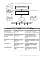
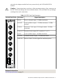
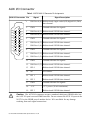
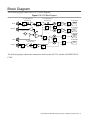
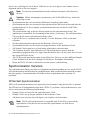
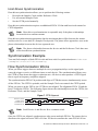
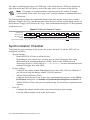
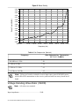
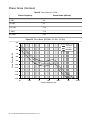
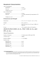
USER MANUAL AND SPECIFICATIONS
NI 5791R
RF Transceiver Adapter Module
The NI 5791 is an RF transceiver adapter module designed to work in conjunction with your
NI FlexRIO™ FPGA module. The NI 5791 features the following connectors and chips:
•
2-channel, 130 MS/s analog-to-digital converter (ADC) with 14-bit accuracy
•
2-channel, 130 MS/s (520 MS/s after interpolation) digital-to-analog converter (DAC)
with 16-bit accuracy
•
LO input and LO output connectors to support LO sharing for multiple-channel
applications
•
Timing chip with clocking options from the backplane and the front panel
•
Programmable attenuators
•
Selectable receive and transmit filters
•
The following front panel connectors:
–
RX IN
–
LO OUT
–
CLK IN
–
CLK OUT
–
LO IN
–
TX OUT
The NI 5791 can upconvert and downconvert RF signals ranging from 200 MHz to 4.4 GHz.
This document contains signal information and lists the specifications of the NI 5791R, which
is composed of the NI FlexRIO FPGA module and the NI 5791. This document also contains
tutorial sections that demonstrate how to acquire data using a LabVIEW FPGA Example VI
and how to create and run your own LabVIEW project with the NI 5791R.
Note NI 5791R refers to the combination of your NI 5791 adapter module and
your NI FlexRIO FPGA module. NI 5791 refers to your NI 5791 adapter module
only.
Note The NI 5791 is only compatible with the NI PXIe-796xR FPGA modules.
Note Before configuring your NI 5791, you must install the appropriate software
and hardware. Refer to the NI FlexRIO FPGA Module Installation Guide and
Specifications for installation instructions.
Note For EMC compliance, operate this device according to the documentation.
The following figure shows an example of a properly connected NI FlexRIO device.
Figure 1. NI FlexRIO Device
NI FlexRIO
Adapter Module
+
NI FlexRIO
FPGA Module
=
NI FlexRIO Device
Related Information
NI 5791 Specifications on page 21
Contents
Electromagnetic Compatibility Guidelines...............................................................................3
Connecting Cables....................................................................................................................4
How to Use Your NI FlexRIO Documentation Set..................................................................4
Key Features.............................................................................................................................6
Configuration............................................................................................................................6
Front Panel and Connector Pinouts...........................................................................................6
AUX I/O Connector..........................................................................................................8
Block Diagram..........................................................................................................................9
NI 5791 Component-Level Intellectual Property (CLIP).......................................................11
5791 CLIP.......................................................................................................................12
Programmable Chips.......................................................................................................13
2 | NI 5791R User Manual and Specifications | ni.com
Using Your NI 5791R with a LabVIEW FPGA Example VI.................................................13
Using the Included Streaming Example..........................................................................14
Creating a LabVIEW Project..........................................................................................14
NI-579x Configuration Design Library..................................................................................16
FPGA VI Requirements..................................................................................................17
Host VI Requirements.....................................................................................................17
Synchronization Overview......................................................................................................17
Synchronization Versions...............................................................................................18
Synchronization Example...............................................................................................19
How Synchronization Works..........................................................................................19
Synchronization Checklist..............................................................................................20
Clocking..................................................................................................................................21
579x Sample Projects..............................................................................................................21
NI 5791 Specifications............................................................................................................21
RX IN..............................................................................................................................22
LO OUT Front Panel Connector.....................................................................................27
CLK IN Front Panel Connector......................................................................................28
CLK OUT Front Panel Connector..................................................................................28
LO IN Front Panel Connector.........................................................................................29
TX OUT Front Panel Connector.....................................................................................29
TX OUT Spurious Responses.........................................................................................31
RX IN and TX OUT Frequency Characteristics.............................................................33
Baseband Characteristics................................................................................................35
AUX I/O (Port 0 DIO <0..3>, Port 1 DIO <0..3>, and PFI <0..3>)...............................35
Compliance and Certifications........................................................................................36
Environment....................................................................................................................37
Installing PXI EMC Filler Panels...................................................................................38
Where to Go for Support.................................................................................................39
Electromagnetic Compatibility Guidelines
This product was tested and complies with the regulatory requirements and limits for
electromagnetic compatibility (EMC) stated in the product specifications. These requirements
and limits are designed to provide reasonable protection against harmful interference when the
product is operated in the intended operational electromagnetic environment.
This product is intended for use in industrial locations. However, harmful interference may
occur in some installations, when the product is connected to a peripheral device or test object,
or if the product is used in residential or commercial areas. To minimize interference with
radio and television reception and prevent unacceptable performance degradation, install and
use this product in strict accordance with the instructions in the product documentation.
NI 5791R User Manual and Specifications | © National Instruments | 3
Furthermore, any modifications to the product not expressly approved by National Instruments
could void your authority to operate it under your local regulatory rules.
Caution To ensure the specified EMC performance, operate this product only with
shielded cables and accessories.
Caution To ensure the specified EMC performance, the length of all I/O cables
must be no longer than 3 m (10 ft).
Caution To ensure the specified EMC performance, you must install PXI EMC
Filler Panels (National Instruments part number 778700-1) in adjacent chassis slots.
Related Information
Installing PXI EMC Filler Panels on page 38
Connecting Cables
1.
Use any shielded 50 Ω SMA cable to connect signals to the connectors on the front panel
of your device.
2.
Use the SHH19–H19–AUX cable (NI part number: 152629-01 or 152629-02) to connect
to the digital I/O (DIO) and programmable function interface (PFI) signals on the
AUX I/O connector. NI recommends using the SCB-19 connector block to access the
DIO and PFI signals.
Related Information
NI 5791 Specifications on page 21
How to Use Your NI FlexRIO
Documentation Set
Refer to Figure 2 and Table 1 to learn how to use your FlexRIO documentation set.
4 | NI 5791R User Manual and Specifications | ni.com
Figure 2. How to Use Your NI FlexRIO Documentation Set.
INSTALL Hardware
and Software
NI FlexRIO FPGA Module
Installation Guide and Specifications
CONNECT Signals
and Learn About
Your Adapter
Module
NI FlexRIO Adapter Module
User Guide and Specifications
PROGRAM Your
NI FlexRIO System
in LabVIEW FPGA
Module
Are
You New to
LabVIEW FPGA
Module?
LEARN About
LabVIEW FPGA
Module
Yes
No
No
LabVIEW FPGA
Module Help
NI FlexRIO
Help
LabVIEW
Examples
Table 1. NI FlexRIO Documentation Locations and Descriptions
Document
Location
Description
NI FlexRIO FPGA
Available from the Start
Module Installation
menu and at ni.com/
Guide and Specifications manuals.
Contains installation instructions for
your NI FlexRIO system and
specifications for your FPGA module.
NI 5791R User Manual
and Specifications (this
document)
Contains signal information,
examples, CLIP details, and
specifications for your adapter
module.
Available from the Start
menu and at ni.com/
manuals.
LabVIEW FPGA Module Embedded in LabVIEW
Help*
Help and at ni.com/
manuals.
Contains information about the basic
functionality of the LabVIEW FPGA
Module.
NI FlexRIO Help
Available from the Start
menu and at ni.com/
manuals.
Contains FPGA Module, adapter
module, and CLIP configuration
information.
LabVIEW Examples
Available in NI Example
Finder.
Contains examples of how to run
FPGA VIs and Host VIs on your
device.
NI 5791R User Manual and Specifications | © National Instruments | 5
Table 1. NI FlexRIO Documentation Locations and Descriptions (Continued)
Document
Location
Description
IPNet
ni.com/ipnet
Contains LabVIEW FPGA functions
and intellectual property to share.
NI FlexRIO product
page
ni.com/flexrio
Contains product information and
data sheets for NI FlexRIO devices.
Key Features
The NI 5791 includes the following key features:
RF
............................................................................
frequency range
200 MHz to 4.4 GHz
Instantaneous bandwidth
............................................................................
100 MHz
ADC
............................................................................
14-bit dual channel at 130 MS/s
DAC
............................................................................
16-bit dual channel at 130 MS/s, interpolated
to 520 MS/s
Phase
............................................................................
noise
<94 dBc/Hz, 10 kHz offset, 2.4 GHz carrier
Dynamic
............................................................................
range
>105 dB
Noise figure
............................................................................
<8 dB at 2 GHz
EVM
............................................................................
<1.5% (RMS)
Receive (RX) IP3
............................................................................
+1 dBm at 2 GHz
Transmit
............................................................................
(TX) IP3
+17 dBm at 2 GHz
Configuration
You can configure the NI 5791 as follows:
•
Instantaneous bandwidth up to 100 MHz
•
1 transmitter channel, 16-bit, 520 MS/s (4× interpolation) (I and Q)
•
1 receiver channel, 14-bit, 130 MS/s (I and Q)
Front Panel and Connector Pinouts
Table 2 shows the front panel connector and signal descriptions for the NI 5791.
Caution To avoid permanent damage to the NI 5791, disconnect all signals
connected to the NI 5791 before powering down the module, and connect signals
6 | NI 5791R User Manual and Specifications | ni.com
only after the adapter module has been powered on by the NI FlexRIO FPGA
module.
Caution Connections that exceed any of the maximum ratings of any connector on
the NI 5791R can damage the device and the chassis. NI is not liable for any damage
resulting from such connections.
Table 2. NI 5791 Front Panel Connectors
Device Front Panel Connector
NATIONAL
INSTRUMENTS
NI 5791
RX IN
Receive channel input, +20 dBm maximum
LO OUT
Local oscillator output, +12 dBm maximum, +0 dBm
nominal
CLK IN
Reference Clock input, 50 Ω single-ended, +20 dBm
maximum
RX IN
LO OUT
CLK IN
Signal Description
CLK OUT Exported clock output, DC-coupled, 0 V to 2 V
LO IN
Local oscillator input, +20 dBm maximum
TX OUT
Transmit channel output, +20 dBm maximum
AUX I/O
Refer to Table 3 for the signal list and descriptions.
CLK OUT
LO IN
TX OUT
AUX
I/O
200MHz - 4.4 GHz
RF Transceiver
Related Information
NI 5791 Specifications on page 21
NI 5791R User Manual and Specifications | © National Instruments | 7
AUX I/O Connector
Table 3. NI 5791 AUX I/O Connector Pin Assignments
AUX I/O Connector Pin
18
16
14
12
10
8
6
4
2
Signal
Signal Description
1
DIO Port 0 (0) Bidirectional single-ended (SE) digital I/O (DIO)
data channel.
2
GND
17
3
DIO Port 0 (1) Bidirectional SE DIO data channel.
15
4
DIO Port 0 (2) Bidirectional SE DIO data channel.
5
GND
6
DIO Port 0 (3) Bidirectional SE DIO data channel.
7
DIO Port 1 (0) Bidirectional SE DIO data channel.
8
GND
9
DIO Port 1 (1) Bidirectional SE DIO data channel.
10
DIO Port 1 (2) Bidirectional SE DIO data channel.
11
GND
12
DIO Port 1 (3) Bidirectional SE DIO data channel.
13
PFI 0
Bidirectional SE DIO data channel.
14
NC
No connect.
15
PFI 1
Bidirectional SE DIO data channel.
16
PFI 2
Bidirectional SE DIO data channel.
17
GND
Ground reference for signals.
18
+5 V
+5 V power (10 mA maximum).
19
PFI 3
Bidirectional SE DIO data channel.
19
Ground reference for signals.
13
11
9
7
5
3
1
Ground reference for signals.
Ground reference for signals.
Ground reference for signals.
Caution The AUX I/O connector accepts a standard, third-party HDMI cable, but
the AUX I/O port is not an HDMI interface. Do not connect the AUX I/O port on the
NI 5791 to the HDMI port of another device. NI is not liable for any damage
resulting from such signal connections.
8 | NI 5791R User Manual and Specifications | ni.com
Block Diagram
The following figure shows the NI 5791 block diagram.
Figure 3. NI 5791 Block Diagram
31.75 dB Maximum
0.25 dB Step
31.75 dB Maximum
0.25 dB Step
TI ADS4246
12 dB
RX IN
4.4 GHz
LPF
LO OUT
RX RF Filter
Bank
90
0
52 MHz
LPF
RX LO Filter
Bank
ADI ADF4351
Synthesizer LO
12 dB
52 MHz
LPF
ADC
14 bit
Noise Reject
LPF
TI ADS4246
ADC
14 bit
Noise Reject
LPF TI DAC3482
DAC
16 bit
LO IN
31.75 dB Maximum
0.25 dB Step
TX LO Filter
Bank
90
0
204 MHz
LPF
TI DAC3482
DAC
16 bit
204 MHz
LPF
TX OUT
4.4 GHz
LPF
TX RF Filter
Bank
44 MHz
HPF
The following figure shows the connections between the NI 5791 and the LabVIEW FPGA
CLIP.
NI 5791R User Manual and Specifications | © National Instruments | 9
Figure 4. NI 5791 Connector Signals and CLIP Signal Block Diagram
NI 5791 Adapter Module
From RF
Mixer
ADC Data
ADC
ADS4246
Gain
From RF
Mixer
To RF Mixer
LabVIEW FPGA CLIP
14
ADC Clock
ADC SPI
ADC
Interface
Sample Clock
DAC Data
DAC
DAC3482
DAC
Interface
16
DAC Clock
To RF Mixer
Rx I
14 Rx Q
14
Tx I
16
Tx Q
16
Synchronize DAC
DAC SPI
CLK IN
CLK OUT
OUT3 OUT2
CLK1 AD9511
REF IN
OUT1
CLK2
OUT 4
SPI
CP
Sample Clock
Sample Clock 2x
PLL
PLL Locked
Sync Clock
VCXO
PLL Loop
Filter
DAC
RF LO
and Attenuators
SPI
SPI
Engine
Register
Bus
Clock
DAC SPI
Enable VCXO
Calibration
EEPROM
Microcontroller
Enable PLL
External Sample CLK
External Ref CLK
AI Gain Control
RF Filter Control
RF Filters
From RF LO
Register Bus Idle
Register Bus Address
Register Bus Read Data
Register Bus Read
Register Write Data
Register Bus Write
Initialization Done
User Error
User Return
User Command Idle
User Command
User Command Commit
User Command Status
User Data 0
User Data 1
LO Locked
DIO Port 0 Rd Data (0)
DIO Port 0 Wr Data (0)
DIO Port 0 Rd Data (1)
DIO Port 0 Wr Data (1)
DIO Port 0 Rd Data (2)
DIO Port 0 Wr Data (2)
DIO Port 0 Rd Data (3)
DIO Port 0 Wr Data (3)
DIO Port 0 (0)
DIO Port 0 (1)
DIO Port 0 (2)
DIO Port 0 (3)
DIO Port 0 WE
DIO Port 1 Rd Data (0)
DIO Port 1 Wr Data (0)
DIO Port 1 Rd Data (1)
DIO Port 1 Wr Data (1)
DIO Port 1 Rd Data (2)
DIO Port 1 Wr Data (2)
DIO Port 1 Rd Data (3)
DIO Port 1 Wr Data (3)
AUX I/O
DIO Port 1 (0)
DIO Port 1 (1)
DIO Port 1 (2)
DIO Port 1 (3)
DIO Port 1 WE
PFI 0 Rd Data
PFI 0 Wr Data
PFI 1 Rd Data
PFI 1 Wr Data
PFI 2 Rd Data
PFI 2 Wr Data
PFI 3 Rd Data
PFI 3 Wr Data
PFI 0
PFI 1
PFI 2
PFI 3
4
The following figure shows the NI 5791 low-pass filter bank.
10 | NI 5791R User Manual and Specifications | ni.com
PFI <0..3> WE
Figure 5. Low-Pass Filter (LPF) Bank
3600 MHz LPF
2400 MHz LPF
1600 MHz LPF
1066 MHz LPF
711 MHz LPF
474 MHz LPF
316 MHz LPF
4400 MHz LPF
NI 5791 Component-Level Intellectual Property
(CLIP)
The LabVIEW FPGA Module includes component-level intellectual property (CLIP) for HDL
IP integration. NI FlexRIO devices support two types of CLIP: user-defined and socketed.
•
User-defined CLIP allows you to insert HDL IP into an FPGA target, enabling VHDL
code to communicate directly with an FPGA VI.
•
Socketed CLIP provides the same IP integration of the user-defined CLIP, but also allows
the CLIP to communicate directly with circuitry external to the FPGA. Adapter module
socketed CLIP allows your IP to communicate directly with both the FPGA VI and the
external adapter module connector interface.
The following figure shows the relationship between an FPGA VI and the CLIP.
NI 5791R User Manual and Specifications | © National Instruments | 11
Figure 6. CLIP and FPGA VI Relationship
NI FlexRIO FPGA Module
FPGA
Adapter Module
CLIP Socket
LabVIEW
FPGA VI
User-Defined
CLIP
Socketed
CLIP
Socketed
CLIP
Socketed
CLIP
Fixed I/O
DRAM 1
CLIP Socket
Fixed I/O
DRAM 0
CLIP Socket
DRAM 0
DRAM 1
Fixed I/O
Adapter
Module
External
I/O Connector
User-Defined
CLIP
The NI 5791 ships with socketed CLIP items that add module I/O to the LabVIEW project.
The NI 5791 ships with the following CLIP item:
5791 CLIP
The 5791 CLIP provides access to I and Q data for one receive channel and one transmit
channel. The CLIP also provides a User Command interface for common configurations of the
baseband clocking, programmable attenuators, receive amplifier, receive and transmit filters,
LO filters, and RF path. You can also import and export the LO.
Configure the baseband clocking using one of the following settings:
•
Internal Sample Clock
•
Internal Sample Clock locked to an external Reference Clock though the CLK IN
connector
•
External Sample Clock through the CLK IN connector
•
Internal Sample Clock locked to an external Reference Clock through the Sync Clock
This CLIP also contains a FAM Registers Bus interface, which is a low-level bus interface that
directly programs registers on all programmable devices, such as the analog-to-digital
converter (ADC) and the digital-to-analog converter (DAC). Programming registers on these
devices allows for more advanced configuration.
Note You cannot configure the LO using the User Command interface. Use the
FAM Registers Bus interface to program the LO synthesizer, then use the User
Command interface to configure the LO filters.
12 | NI 5791R User Manual and Specifications | ni.com
Refer to the NI FlexRIO Help for more information about NI FlexRIO CLIP items,
configuring the NI 5791 with a socketed CLIP, and a list of available socketed CLIP signals.
Programmable Chips
You can program the following chips from the CLIP.
Table 4. Programmable Chips
Chip
Part Number
ADC
TI ADS4246
DAC
TI DAC3482
Clock Distribution
ADI AD9511
Frequency/Phase Adjust DAC
ADI AD5541
EEPROM
SST25VF080B
Programmable RF Attenuator
Peregrine PE43703
Using Your NI 5791R with a LabVIEW FPGA
Example VI
Note You must install the software before running this example. Refer to the
NI FlexRIO FPGA Installation Guide and Specifications for more information about
installing your software.
The NI FlexRIO Adapter Module Support software includes an example project to help you
get started creating your LabVIEW FPGA application. This section explains how to use an
existing LabVIEW FPGA example project to generate and acquire samples with the NI 5791R.
This example requires at least one SMA cable for connecting signals to your NI 5791R.
Note The examples available for your device are dependent on the version of the
software and driver you are using. For more information about which software
versions are compatible with your device, visit ni/com/info, enter
rdsoftwareversion in the text field, and click the NI FlexRIO link in the results.
The NI 5791R example project includes the following components:
•
A LabVIEW FPGA VI that can be compiled and run on the FPGA embedded in the
hardware
•
At least one VI that runs on Windows and interacts with the LabVIEW FPGA VI
Note In the LabVIEW FPGA Module software, NI FlexRIO adapter modules are
referred to as IO Modules.
NI 5791R User Manual and Specifications | © National Instruments | 13
Using the Included Streaming Example
Complete the following steps to run an example that acquires a waveform using the NI 5791.
1. Connect an antenna to the RX IN connector on the front panel of the NI 5791.
2. Launch LabVIEW.
3. Select File»Open Project.
4. Navigate to <labview>\examples\instr\ni579x\Streaming.
5.
6.
Select Streaming.lvproj.
In the Project Explorer window, select Rx Streaming (Host).vi under My Computer to
open the host VI. The Open FPGA VI Reference function in this VI uses the NI 7966R as
the FPGA target by default. If you are using an NI FlexRIO FPGA module other than the
NI 7966R, complete the following steps to change to the FPGA VI to support your target.
a) Specify the center frequency in the LO frequency [Hz] control.
b) On the block diagram, right-click the Open FPGA VI Reference (PXI-7966R)
function and select Configure Open FPGA VI Reference.
c) In the Configure Open FPGA VI Reference dialog box, click the Browse button
next to the Bitfile button.
d) In the Select Bitfile dialog box that opens, select the bitfile for your desired target.
The bitfile name is based on the adapter module, example type, and FPGA module.
e) Click the Select button.
f) Click OK in the Configure Open FPGA VI Reference dialog box.
g) Save the VI.
7. On the front panel, in the RIO Device pull-down menu, select an NI 5791 resource that
corresponds with the target configured in step 6.
8. Configure your measurement.
a) Specify the center frequency in the LO frequency [Hz] control.
b) Specify the reference level in the reference level [dBm] control.
c) Specify the sample rate in the sample rate [S/s] control.
9. Click the Run button to run the VI.
10. The VI acquires data and displays the captured waveform on the Power Level, Power
Spectrum, I Data, and Q Data graphs.
11. Click the STOP button to stop the VI.
12. Close the VI.
Creating a LabVIEW Project
This section explains how to set up your target and create an FPGA VI and host VI for data
communication. This section focuses on proper project configuration, proper CLIP
configuration, and how to access NI 5791 I/O nodes.
Creating a Project
1.
2.
3.
Launch LabVIEW, or if LabVIEW is already running, select File»Create Project.
In the Create Project dialog box, select LabVIEW FPGA Project and click Finish.
Select FlexRIO on My Computer and click Next.
14 | NI 5791R User Manual and Specifications | ni.com
4.
5.
6.
Either discover a LabVIEW FPGA target in your system or create a new system and
specify an FPGA target for which to construct a project.
Click Finish in the Project Preview dialog box.
Click File»Save and specify a name for the project.
Creating an FPGA Target VI
1.
2.
3.
4.
5.
6.
7.
8.
9.
In the Project Explorer window, expand FPGA Target.
Right-click FPGA Target and select New»FPGA Base Clock.
In the Resource pull-down menu, select 200 MHz Clock and click OK.
Right-click IO Module in the Project Explorer window and select Properties.
Select Enable IO Module.
Select the NI 5791 from the IO Module list. The available CLIP for the NI 5791 is
displayed in the Component Level IP pane.
Select NI 5791 in the Name list of the Component Level IP pane.
In the Clock Selections category, select 200 MHz Clock from the pull-down menu for
Clock 200 MHz. Leave Clock 40 MHz configured as the Top-Level Clock.
Click OK.
Note Configuring these clocks is required for proper CLIP operation. Refer to
the NI 5791 CLIP topics in the NI FlexRIO Help for more information about
configuring your clocks.
10. Select File»Open and select <labview>\instr.lib\ni579x\config\v1\FPGA
\Public\ni579x Config FPGA Template.vi.
11. Select File»Save As.
12. Select Copy»Open Additional Copy and check Add Copy to <your project
name>.lvproj.
13. Select the destination folder for the new file, specify a file name, and click OK. Use this
FPGA VI with the NI-579x Configuration Design Library.
14. In the Project Explorer window, expand IO Module Tree View. Use any of the
elements under IO Module (NI 5791 : NI 5791) in the block diagram of the FPGA VI.
Note Use Rx I, Rx Q, Tx I, and Tx Q in a single-cycle Timed Loop using the
Sample Clock provided by the CLIP. Sample Clock x2 runs at twice the rate of
the Sample clock. The DSP and Synchronization Design Libraries use Sample
Clock x2.
15. Add any FPGA code, controls, and indicators that you need. Refer to
Streaming.lvproj for example FPGA code, controls, and indicators.
16. Click the Run button. LabVIEW creates a default build specification and begins
compiling the VI. The Generating Intermediate Files window displays the code
generation process. The Compilation Status window displays the progress of the
compilation. The compilation takes several minutes.
17. Click Close in the Compilation Status window.
18. Save and close the VI .
19. Save the project.
NI 5791R User Manual and Specifications | © National Instruments | 15
Creating a Host VI
1.
In the Project Explorer window, right-click My Computer and select New»VI to open
a blank VI.
2.
Select Window»Show Block Diagram to open the VI block diagram.
3.
Add the Open FPGA VI Reference function from the FPGA Interface palette to the block
diagram.
4.
Right-click the Open FPGA VI Reference function and select Configure Open FPGA
VI Reference.
5.
In the Configure Open FPGA VI Reference dialog box, select VI in the Open section.
6.
In the Select VI dialog box, select your project under your device and click OK.
7.
Click OK in the Configure Open FPGA VI Reference dialog box. The target name
appears under the Open FPGA VI Reference function in the block diagram.
8.
Open the FPGA Interface palette.
9.
Add any Read/Write Control or Invoke Method nodes necessary to configure and
communicate with your FPGA VI.
10. Add the Close FPGA VI Reference function to your block diagram.
11. Wire the FPGA VI Reference function to the Close FPGA VI Reference function.
12. Save and close the VI.
13. Save the project.
Run the Host VI
1.
Open the front panel of your host VI.
2.
Click the Run button to run the VI.
NI-579x Configuration Design Library
The NI-579x Configuration Design Library consists of host and FPGA VIs that provide an
interface to configure the hardware on the NI 5791.
The library allows you to perform the following actions:
•
Configure the mixers
•
Configure the RF signal path, including attenuators, amplifiers, and filters
•
Read from and write to the EEPROM
•
Configure the reference level for the Rx channel and the output power for the Tx channel
•
Configure the clocks
•
Reinitialize the CLIP
•
Query for CLIP errors
The NI-579x Configuration Design Library relies on the Register Bus Design Library. The
Register Bus provides a packet-based configuration interface which exposes all of the address
spaces of the configurable chips and subsystems of the adapter module, without requiring
hundreds of controls and indicators on your FPGA VI front panel.
16 | NI 5791R User Manual and Specifications | ni.com
The NI-579x Configuration Design Library host VIs all require a register bus object for the
device you want to configure. Create the register bus object using Open Session.vi, or use
ni579x Open.vi.
For more information about how to use the NI-579x Configuration Design Library, refer to the
example located at <labview>\examples\instr\ni579x\Streaming
\Streaming.lvproj.
FPGA VI Requirements
Copy all the controls, indicators, and FPGA logic required to use the NI-579x Configuration
Design Library from the following VI: <labview>\instr.lib\ni579x\Config
\v1\FPGA\Public\ni579x Config FPGA Template.vi. The FAM Support installer
installs this VI on your system.
Configure your FPGA target to contain a FIFO with the following configuration.
•
Name: reg.host instruction fifo 0
•
Type: Host to Target - DMA
•
Requested number of elements: 1,023
•
Data type: U64
•
Arbitration for read: Arbitrate if multiple requestors only
•
Number of elements per read: 1
Host VI Requirements
Configure your host VI to use the NI-579x Configuration Design Library using the following
configuration:
1. Create a Register Bus object for your device and initialize the session using ni579x
Open.vi.
2.
Use any of the NI-579x Configuration Design Library Host VIs using the Register Bus
object returned by the ni579x Open VI.
3.
To access the Host VIs, select Functions»Instrument I/O»Instrument Drivers»
NI-579x Configuration.
4.
Close the session using the ni579x Close VI.
Synchronization Overview
Synchronization coordinates Sample Clock cycles across multiple NI FlexRIO devices.
Sources of error, such as common clock propagation delay, cabling and cable lengths, analog
delays in the FPGA module and/or adapter module, and skew/jitter in the common clock, can
affect frequency and phase relationships between devices.
Use the programming example to synchronize across multiple NI FlexRIO adapter modules.
Synchronization aligns the devices so that the devices are synchronized to the nearest Sample
Clock cycle. The devices may be offset by up to one half of one Sample Clock cycle, if the
NI 5791R User Manual and Specifications | © National Instruments | 17
devices are ±180 degrees out of phase. If the devices are zero degrees out of phase, device
alignment offset is also zero degrees.
Note For the best synchronization results, minimize the phase offset between
devices.
•
•
•
•
•
•
•
•
•
•
Caution Before attempting to synchronize your NI FlexRIO devices, notice the
following caveats:
Synchronization does not account for differences in analog signal paths.
Synchronization does not account for data pipeline delays that occur before and after the
synchronization VIs. For example, synchronization does not account for ADC/DAC
pipeline delays.
The synchronized edge is always delayed relative to the unsynchronized edge. The
application is responsible for accounting for this delay, if necessary. The synchronization
VIs provide the actual synchronization delay value.
Lock all devices to a common time reference. Use the Reference Clock as the time
reference.
Set the synchronization registers for the Reference Clock to zero.
Synchronization does not account for propagation delays of the Reference Clock.
All Sample Clocks must have a fixed phase relationship with each other.
The Common Periodic Time Reference (CPTR) period must be greater than the
maximum propagation delay of a signal from the master device to any slave device across
the selected FPGA I/O line.
The CPTR period must be the same across all devices. Devices can have different Sample
Clock frequencies if the device Sample Clocks have a fixed phase relationship.
Route the FPGA I/O lines to all the devices that you are synchronizing.
Synchronization Versions
The synchronization library provides two alignment methods depending on user needs: FPGA
self-synchronization and host-driven synchronization. Both synchronization methods produce
the same quality of synchronization, but differ in their requirements and versatility of
operation.
FPGA Self-Synchronization
FPGA self-synchronization does not require host involvement. Using the host VIs is optional.
The FPGAs can all independently align their CPTRs. To perform a self-synchronization, your
devices must meet the following requirements:
•
Sample Clocks are locked to the same Reference Clock.
•
Sample Clocks are an integer multiple of the Reference Clock.
•
All the devices are fewer than 90 degrees out-of-phase with each other.
Note FPGA self-synchronization is repeatable only if the devices meet all the
requirements. If the devices do not meet the requirements, use host-driven
synchronization.
18 | NI 5791R User Manual and Specifications | ni.com
Host-Driven Synchronization
Host-driven synchronization allows you to perform the following actions:
•
Decouple the Sample Clock and the Reference Clock
•
Use an external Sample Clock
•
Set the CPTR period manually
Host-driven synchronization requires an additional FPGA I/O line and host involvement for
CPTR alignment.
Note Host-driven synchronization is repeatable only if the phase relationships
between devices remain constant.
Host-driven synchronization guarantees that the maximum phase offset between the master
and slave device is one-half of a Sample Clock period. The phase offset approaches zero as the
phase relationships between the devices approach zero.
Note The phase relationship between the device and the Reference Clock does not
affect host-driven synchronization.
Synchronization Example
You can find examples of both FPGA code and host code for synchronization at <labview>
\examples\instr\ni579x\Streaming.
How Synchronization Works
When you share triggers between multiple devices, propagation delays on the signal path
cause the trigger to arrive at different times on each device. The synchronization library uses
the CPTR to slow down the trigger evaluation rate. All devices must produce a CPTR signal
that is equal in frequency and phase-aligned.
The synchronization FPGA VIs produce and align a CPTR that occurs simultaneously across
all the FPGAs. The CPTR is periodic, and the Sample Clock rate controls the CPTR period.
When you power on the FPGAs, the CPTRs are not aligned. The alignment FPGA VI and the
host VI align the CPTRs. The following figure shows the relationship between the CPTRs, the
Reference Clock, and the Sample Clock.
Figure 7. CPTR Alignment
Reference Clock
Sample Clock
CPTR Device A
CPTR Device B
Note Lock Device A and Device B to a common clock.
Once the CPTRs are aligned, synchronize an edge across multiple FPGAs. The master device
distributes the signal across an FPGA I/O line. All devices monitor the same FPGA I/O line.
NI 5791R User Manual and Specifications | © National Instruments | 19
The edge is synchronized at the next CPTR edge. After all the device CPTRs are aligned, an
edge sent out on the FPGA I/O lines is read at the same clock cycle across all the devices.
Note The quality of synchronization is only as good as the quality of Sample
Clock locking. Some static skew may exist. You can calibrate to eliminate this skew
if necessary.
The following figure shows the relationship between the time that the master device reads a
Reference Trigger (Ref Trig) and the time that all the devices read the synchronized version of
the Reference Trigger (Synchronized Ref Trig). This synchronization requires CPTR alignment
on all the devices.
Figure 8. Reading the Reference Triggers
Sample Clock
CPTR Device A
CPTR Device B
Ref Trig
Synchronized Ref Trig
Synchronization Checklist
Verify that the project settings in the system, the project, the host VI, and the FPGA VI are
configured as follows.
•
System settings:
–
Route the FPGA I/O lines to all the devices.
–
Depending on your chassis size, you may have to route PXI trigger lines using
Measurement & Automation Explorer (MAX). Refer to the Measurement &
Automation Explorer (MAX) Help at ni.com/manuals for more information about
routing PXI trigger lines with MAX.
•
Project settings:
–
Configure the adapter module IoModSyncClock (either PXI_CLK10 or DStarA) if
you are not driving the adapter module CLK IN connector.
–
Add the FPGA Reference Clock.
–
Configure the Reference Clock to have zero synchronization registers. In the FPGA
IO Property dialog box, set Number of Synchronization Registers for Read to 0.
–
Add the FPGA I/O lines that you are synchronizing. Do not remove synchronization
registers.
•
Host VI:
–
Configure the adapter module clock source based on the project settings.
–
Lock the adapter module clock to the clock source.
20 | NI 5791R User Manual and Specifications | ni.com
–
–
•
Run the Synchronization VI.
Refer to the example FPGA code at
<labviewdir>\examples\instr\ni579x\Streaming.
FPGA VI:
–
Configure the CPTR period. The synchronization library ensures that the CPTR
period is the same on the host and the FPGA.
–
Refer to the example FPGA code at
<labviewdir>\examples\instr\ni579x\Streaming.
Clocking
The NI 5791 clock source controls the sample rate and other timing functions on the device.
The following table contains information about the possible NI 5791 clock sources.
Table 5. NI 5791R Clock Sources
Clock
Frequency
Source Options
Sample Clock
130 MHz
•
•
Free-running and internally sourced
External through the CLK IN front panel connector
Reference Clock
10 MHz
•
•
•
Free-running and internally sourced
External through the CLK IN front panel connector
Sourced through PXI-CLK
579x Sample Projects
The NI 5791 software contains sample projects that are a starting point for application
development. The projects are available in LabVIEW under Create Project»Sample
Projects»NI-579X.
NI 5791 Specifications
Specifications are warranted by design and under the following conditions unless otherwise
noted:
•
Chassis fan speed is set to High. In addition, NI recommends using slot blockers and
EMC filler panels in empty module slots to minimize temperature drift.
•
The NI 5791 uses NI LabVIEW and LabVIEW FPGA software.
National Instruments RF devices are capable of acquiring and/or generating signals within
common Medical Implantable Communication System (MICS) frequency bands. NI RF
devices are tested and verified in manufacturing for several measurements. For more
NI 5791R User Manual and Specifications | © National Instruments | 21
information about RF device applications, visit to contact a National Instruments branch
office.
Specifications describe the warranted product performance over ambient temperature ranges of
0 °C to 55 °C, unless otherwise noted.
Specifications are subject to change without notice. For the most recent device specifications,
visit ni.com/manuals.
Typical values describe useful product performance beyond specifications that are not covered
by warranty and do not include guardbands for measurement uncertainty or drift. Typical
values may not be verified on all units shipped from the factory. Unless otherwise noted,
typical values cover the expected performance of units over ambient temperature ranges of
23 °C ± 5 °C with a 90% confidence level, based on measurements taken during development
or production.
Nominal values (or supplemental information) describe additional information about the
product that may be useful, including expected performance that is not covered under
Specifications or Typical values. Nominal values are not covered by warranty.
Related Information
Front Panel and Connector Pinouts on page 6
Connecting Cables on page 4
NI 5791 User Manual and Specifications on page 1
RX IN
Amplitude Range
............................................................................
RX input attenuation
0 dB to 63.5 dB in 0.25 dB steps, 6 µs switch
time
Absolute Amplitude Accuracy
Note All values are typical.
Table 6. Absolute Amplitude Accuracy
Center Frequency
Absolute Amplitude Accuracy,
Temperature 23 °C ± 5 °C (dB)
>200 MHz to 1 GHz
0.55
>1 GHz to 2 GHz
0.55
>2 GHz to 3 GHz
0.65
22 | NI 5791R User Manual and Specifications | ni.com
Table 6. Absolute Amplitude Accuracy (Continued)
Center Frequency
Absolute Amplitude Accuracy,
Temperature 23 °C ± 5 °C (dB)
>3 GHz to 3.9 GHz
1.3
>3.9 GHz to 4.4 GHz
1.5
Note Absolute amplitude accuracy uses a correction coefficient in EEPROM to
improve performance. Performance is verified over the first 45 dB of RX
attenuation.
Note Correction coefficients in EEPROM are valid only when the baseband
amplifier is in the signal path.
Noise Density
Table 7. Noise Density
Center Frequency
Average Noise Level (dBm/Hz),
Temperature 23 °C ± 5 °C
>200 MHz to 1 GHz
-163
>1 GHz to 2 GHz
-163
>2 GHz to 3 GHz
-162
>3 GHz to 3.5 GHz
-160
>3.5 GHz to 3.9 GHz
-158
>3.9 GHz to 4.4 GHz
-148
Note Performance is measured with an input reference level of -48 dBm and
with 0 dB of RX attenuation.
NI 5791R User Manual and Specifications | © National Instruments | 23
Figure 9. Noise Density
–153
–154
–155
–156
Noise Floor (dBm/Hz)
–157
–158
–159
–160
–161
–162
–163
–164
–165
–166
–167
–168
200.0 M
1.0 G
1.50 G
2.0 G
2.5 G
3.0 G
3.5 G
4.0 G 4.4 G
Frequency (Hz)
Table 8. Gain Compression (Nominal)
Frequency
Gain Compression, Temperature
23 °C ± 5 °C (dBm)
>200 MHz to 1 GHz
-20
>1 GHz to 2 GHz
-18
>2 GHz to 3.9 GHz
-15
>3.9 GHz to 4.4 GHz
-12
Note Values are based on stimulus of two input tones spaced 100 MHz apart,
with 0 dB of RX attenuation on the receive path and with one tone placed out of
band.
Voltage Standing Wave Ratio (VSWR)
Note All values are nominal.
Input impedance
............................................................................
50 Ω
24 | NI 5791R User Manual and Specifications | ni.com
Input VSWR with 10 dB of RX attenuation
<1.3 GHz
....................................................................
1.5:1
1.3 GHz < f < 3 GHz
....................................................................
1.1:1
>3 GHz
....................................................................
1.9:1
Spurious Responses
Note All responses are typical.
Non-input-related residual spurs
<3 GHz
....................................................................
<-101 dBm
3 GHz to 3.9 GHz
....................................................................
<-100 dBm
≥3.9 GHz
....................................................................
<-91 dBm
Note Performance is measured with 0 dB of RX attenuation and a 1.5 kHz
resolution bandwidth (RBW).
RX LO Residual Power
Note All values are nominal.
Table 9. Receiver LO Residual Power
Center Frequency
Residual Power, Temperature 23 °C ± 5 °C (dBFS)
>200 MHz to 1 GHz
-42
>1 GHz to 2 GHz
-52
>2 GHz to 3 GHz
-52
>3 GHz to 3.9 GHz
-52
>3.9 GHz to 4.4 GHz
-52
Note Receiver LO suppression is measured at the same RX attenuation after an
I/Q correction.
RX Sideband Image Suppression
Note All values are nominal.
NI 5791R User Manual and Specifications | © National Instruments | 25
Table 10. Sideband Image Suppression
Center Frequency
Temperature 23 °C ± 5 °C (dBc)
>200 MHz to 1 GHz
-39
>1 GHz to 2 GHz
-58
>2 GHz to 3 GHz
-54
>3 GHz to 3.9 GHz
-45
>3.9 GHz to 4.4 GHz
-35
Note The image suppression specifications hold at the center frequency of the
acquired instantaneous bandwidth after the device performs a single recent point
I/Q impairment self-correction.
RX Third Order Intermodulation Distortion (IP3)
Note All values are nominal.
Table 11. RX IP3
Frequency
Temperature 23 °C ± 5 °C (dBm)
>200 MHz to 1 GHz
-2
>1 GHz to 2 GHz
-1
>2 GHz to 3 GHz
0
>3 GHz to 3.9 GHz
1
>3.9 GHz to 4.4 GHz
1
Note Values are based on two input tones spaced 1 MHz apart such that the
tones are 6 dB less than full-scale with 0 dB of RX attenuation.
Dynamic Range
Note All values are nominal.
26 | NI 5791R User Manual and Specifications | ni.com
Table 12. Dynamic Range at 900 MHz
Reference Level
(dBm)
IP3 (dBm)
Noise Floor
(dBm/Hz)
Dynamic Range (dB)
5
24
-135
106
-5
14
-145
106
-15
4
-155
106
-25
0
-163
109
Note The signal level of each tone is set to 6 dB less than the reference level to
prevent overload. Dynamic range = 2/3 × (IMD3 – Noise Floor)
Table 13. Dynamic Range at 2,400 MHz
Reference Level
(dBm)
IP3 (dBm)
Noise Floor
(dBm/Hz)
Dynamic Range (dB)
5
22
-135
105
-5
12
-145
105
-15
3
-155
105
-25
1
-163
109
Note The signal level of each tone is set to 6 dB less than the reference level to
prevent overload. Dynamic range = 2/3 × (IP3 – Noise Floor)
LO OUT Front Panel Connector
............................................................................
Frequency range
200 MHz to 4.4 GHz
Frequency resolution
............................................................................
1,000 kHz
Output power
<2.4 GHz
....................................................................
0 dBm ± 3 dB, nominal
≥2.4 GHz
....................................................................
-3 dBm ± 3 dB, nominal
Output impedance
............................................................................
50 Ω, nominal
Output VSWR
............................................................................
1.78:1
Amplitude settling time
............................................................................
<0.25 dB in <10 ms, typical
Maximum DC voltage
............................................................................
±0.5 VDC
NI 5791R User Manual and Specifications | © National Instruments | 27
Figure 10. LO Output Power
10
9
LO Output Power (dBm)
8
7
6
5
4
3
2
1
0
0
500 M 1E+09 1.5E+09 2E+09 2.5E+09 3E+09 3.5E+09 4E+09 4.5E+09 5E+09
LO Frequency (Hz)
Note For frequencies above 2.8 GHz, the gain is <0 dB. The NI 5791 can daisy
chain up to eight channels of adapter modules below 2.8 GHz without external
amplification. For frequencies above 2.8 GHz, NI recommends using external LO
distribution amplifiers if more than two adapter modules share LOs.
CLK IN Front Panel Connector
............................................................................
Frequency
10 MHz
Amplitude
Square
....................................................................
0.7 Vpk-pk to 5.0 Vpk-pk into 50 Ω, typical
....................................................................
Sine
1.4 Vpk-pk to 5.0 Vpk-pk (1 VRMS to 3.5 VRMS)
into 50 Ω, typical
............................................................................
Input impedance
50 Ω, nominal
Coupling
............................................................................
AC
CLK OUT Front Panel Connector
Frequency
Reference
....................................................................
Clock
10 MHz
Sample Clock
....................................................................
130 MHz
28 | NI 5791R User Manual and Specifications | ni.com
Amplitude
............................................................................
1.65 Vpk-pk into 50 Ω, nominal
............................................................................
Output impedance
50 Ω, series, nominal
Coupling
............................................................................
AC
LO IN Front Panel Connector
Frequency
............................................................................
range
200 MHz to 4.4 GHz
Input power
<2.4 GHz
....................................................................
3 dBm ± 3 dB, nominal
≥2.4 GHz
....................................................................
0 dBm ± 3 dB, nominal
Input impedance
............................................................................
50 Ω
Input VSWR
............................................................................
1.78:1
Absolute maximum power
............................................................................
+15 dBm
Maximum
............................................................................
DC power
±0.5 VDC
TX OUT Front Panel Connector
Amplitude Characteristics
Power range
....................................................................
Output
Noise floor to +8 dBm, nominal
Output resolution
....................................................................
0.25 dB, nominal
Amplitude settling time
....................................................................
<0.5 dB within 1 ms, nominal
Absolute Amplitude Accuracy
Note All values are typical.
Table 14. Absolute Amplitude Accuracy
Frequency
Temperature 23 °C ±5 °C (dB)
>200 MHz to 1 GHz
0.8
1 GHz to 2 GHz
1.3
2 GHz to 3 GHz
1.3
NI 5791R User Manual and Specifications | © National Instruments | 29
Table 14. Absolute Amplitude Accuracy (Continued)
Frequency
Temperature 23 °C ±5 °C (dB)
3 GHz to 4.4 GHz
1.8
Note Absolute amplitude accuracy uses a correction coefficient in EEPROM to
improve performance. The TX amplitude accuracy applies to the output power
level from -12 dBm to -4 dBm.
Figure 11. TX Output Power
TX Output Power (dBm)
10.0
9.5
9.0
8.5
8.0
7.5
7.0
6.5
6.0
5.5
5.0
4.5
4.0
3.5
3.0
2.5
2.0
1.5
1.0
500.0 m
0.0
–500.0 m
–1.0
200.0 M
1.0 G
1.5 G
2.0 G
2.5 G
3.0 G
3.5 G
4.0 G 4.4 G
Frequency (Hz)
Noise Density
Note All values are typical.
Table 15. Noise Density
Frequency
Temperature 23 °C ±5 °C (dBm/Hz)
>200 MHz to 1 GHz
-138
>1 GHz to 2 GHz
-138
30 | NI 5791R User Manual and Specifications | ni.com
Table 15. Noise Density (Continued)
Frequency
Temperature 23 °C ±5 °C (dBm/Hz)
>2 GHz to 3 GHz
-130
>3 GHz to 4.4 GHz
-130
Note Performance is measured with 0 dB of TX attenuation.
Output Voltage Standing Wave Ratio (VSWR)
<2.0
............................................................................
GHz
1.6:1
≥2.0 GHz and <3.0 GHz
............................................................................
1.4:1
≥3.0 GHz
............................................................................
1.7:1
Note The VSWR is measured with 10 dB of TX attenuation.
TX OUT Spurious Responses
Third Order Intermodulation (IP3)
Note All values are typical.
Table 16. IP3
Frequency
Temperature 23 °C ± 5 °C (dBm)
>200 MHz to 1 GHz
19
>1 GHz to 2 GHz
17
>2 GHz to 3 GHz
13
>3 GHz to 3.9 GHz
11
>3.9 GHz to 4.4 GHz
8
Note Values are based on two input tones spaced 1.3 MHz apart with 5 dB of
TX attenuation.
NI 5791R User Manual and Specifications | © National Instruments | 31
Second Order Intermodulation (IP2)
Note All values are typical.
Note All values are typical.
Table 17. IP2
Frequency
Temperature 23 °C ±5 °C (dBm)
>200 MHz to 1 GHz
25
>1 GHz to 2 GHz
25
>2 GHz to 3 GHz
25
>3 GHz to 4.4 GHz
35
Note Values are based on two input tones spaced 1.3 MHz apart with 5 dB of
TX attenuation.
TX Sideband Image Suppression
Note All values are nominal.
Table 18. Image Suppression
Frequency
Temperature 23 °C ±5 °C (dBc)
>200 MHz to 1 GHz
-50
>1 GHz to 2 GHz
-50
>2 GHz to 3 GHz
-50
>3 GHz to 4.4 GHz
-45
Note The image suppression specifications hold at the center frequency of the
transmitted instantaneous bandwidth after the device performs a recent single
point I/Q impairment self-correction.
TX LO Residual Power
Note All values are typical.
32 | NI 5791R User Manual and Specifications | ni.com
Table 19. TX LO Residual Power
Frequency
Temperature 23 °C ±5 °C (dBm)
>200 MHz to 1 GHz
-48
>1 GHz to 2 GHz
-48
>2 GHz to 3 GHz
-48
>3 GHz to 4.4 GHz
-45
Note This specification holds at the center frequency of the transmitted
instantaneous bandwidth, 100 MHz maximum after the device performs a recent
single point I/Q impairment self-correction. The measurement is performed with
0 dB of TX attenuation.
RX IN and TX OUT Frequency Characteristics
Frequency
............................................................................
range
200 MHz to 4.4 GHz
Instantaneous bandwidth
............................................................................
100 MHz
............................................................................
Tuning
resolution1
<250 kHz
LO step size2
....................................................................
Integer mode
4 MHz, 6 MHz, 12 MHz, 24 MHz step sizes
Fractional
....................................................................
mode
100 kHz step size
Frequency Settling Time
............................................................................
Settling time3
<100 µs per 50 MHz step
1
2
3
Tuning resolution combines LO step size capability and frequency shift DSP
implemented on the FPGA.
Enable fractional mode and use a 100 kHz LO step size with all LO step size specifications.
This settling time specification only includes frequency settling time, and it excludes
any residual amplitude settling that may occur as a result of large frequency changes.
Driver and operating system timing can affect transition times. This specification
reflects only hardware settling.
NI 5791R User Manual and Specifications | © National Instruments | 33
Phase Noise (Nominal)
Table 20. Phase Noise at 2.4 GHz
Offset Frequency
Phase Noise (dBc/Hz)
1 kHz
-90
10 kHz
-94
100 kHz
-104
1 MHz
-130
10 MHz
-140
Figure 12. Phase Noise (900 MHz, 2.4 GHz, 4.4 GHz)
–40
4.4 GHz
2.4 GHz
900 MHz
–50
Phase Noise (dBc/Hz)
–60
–70
–80
–90
–100
–110
–120
–130
–140
10
100
1k
10 k
100 k
Offset Frequency (Hz)
34 | NI 5791R User Manual and Specifications | ni.com
1M
10 M
Baseband Characteristics
ADC (TI ADS4246)4
Resolution
....................................................................14 bits
Data rate
....................................................................
130 MS/s5
Samples per cycle
....................................................................
1
DAC (TI DAC3482)
Resolution
....................................................................
16 bits
Data rate
....................................................................
130 MS/s (automatically interpolated to 520
MS/s)
Samples per cycle
....................................................................
1
Dimensions and Weight
............................................................................
Dimensions
12.9 × 2.0 × 12.1 cm (5.1 × 0.8 × 4.7 in)
Weight
............................................................................
413 g (14.6 oz)
I/O
............................................................................
RX in, RX out, LO in, LO out, 10 MHz, 10
MHz out
Power
............................................................................
6 W, nominal, with one LO turned on
AUX I/O (Port 0 DIO <0..3>, Port 1 DIO <0..3>, and
PFI <0..3>)
General Characteristics
............................................................................
Number of channels
12 bidirectional (8 DIO and 4 PFI)
Connector type
............................................................................
HDMI
Interface standard
............................................................................
3.3 LVCMOS
Interface logic
Maximum VIL
....................................................................
0.8 V
Minimum VIH
....................................................................
2.0 V
Maximum
....................................................................
VOL
0.4 V
....................................................................
Minimum VOH
2.7 V
Maximum VOH
....................................................................
3.6 V
4
5
ADCs and DACs are dual-channel components with each channel assigned to I and Q, respectively.
Use the Fractional Interpolation and Decimation DSP blocks implemented in the LabVIEW FPGA
target to decimate and interpolate the data.
NI 5791R User Manual and Specifications | © National Instruments | 35
....................................................................
Z
50 Ω ± 20%
OUT
I....................................................................
±2 mA
OUT (DC)
Pull-down
............................................................................
resistor
150 kΩ
Recommended operating voltage
............................................................................
-0.3 V to 3.6 V
Overvoltage protection
............................................................................
±10 V
Maximum toggle frequency
............................................................................
6.6 MHz
+5 V maximum power
............................................................................
10 mA
+5 V voltage tolerance
............................................................................
4.2 V to 5 V
Compliance and Certifications
Safety
This product is designed to meet the requirements of the following electrical equipment safety
standards for measurement, control, and laboratory use:
•
IEC 61010-1, EN 61010-1
•
UL 61010-1, CSA 61010-1
Note For UL and other safety certifications, refer to the product label or the Online
Product Certification section.
Electromagnetic Compatibility
This product meets the requirements of the following EMC standards for electrical equipment
for measurement, control, and laboratory use:
•
EN 61326-1 (IEC 61326-1): Class A emissions; Basic immunity
•
EN 55011 (CISPR 11): Group 1, Class A emissions
•
AS/NZS CISPR 11: Group 1, Class A emissions
•
FCC 47 CFR Part 15B: Class A emissions
•
ICES-001: Class A emissions
Note In the United States (per FCC 47 CFR), Class A equipment is intended for
use in commercial, light-industrial, and heavy-industrial locations. In Europe,
Canada, Australia, and New Zealand (per CISPR 11), Class A equipment is intended
for use only in heavy-industrial locations.
Note Group 1 equipment (per CISPR 11) is any industrial, scientific, or medical
equipment that does not intentionally generate radio frequency energy for the
treatment of material or inspection/analysis purposes.
Note For EMC declarations and certifications, and additional information, refer to
the Online Product Certification section.
36 | NI 5791R User Manual and Specifications | ni.com
CE Compliance
This product meets the essential requirements of applicable European Directives, as follows:
•
2006/95/EC; Low-Voltage Directive (safety)
•
2004/108/EC; Electromagnetic Compatibility Directive (EMC)
Online Product Certification
To obtain product certifications and the DoC for this product, visit ni.com/certification, search
by model number or product line, and click the appropriate link in the Certification column.
Environmental Management
NI is committed to designing and manufacturing products in an environmentally responsible
manner. NI recognizes that eliminating certain hazardous substances from our products is
beneficial not only to the environment but also to NI customers.
For additional environmental information, refer to the Minimize Our Environmental Impact
web page at ni.com/environment. This page contains the environmental regulations and
directives with which NI complies, as well as other environmental information not included in
this document.
Waste Electrical and Electronic Equipment (WEEE)
EU Customers At the end of the product life cycle, all products must be sent to a
WEEE recycling center. For more information about WEEE recycling centers,
National Instruments WEEE initiatives, and compliance with
WEEE Directive 2002/96/EC on Waste Electrical and Electronic Equipment, visit
ni.com/environment/weee.htm.
电子信息产品污染控制管理办法(中国 RoHS)
中国客户 National Instruments 符合中国电子信息产品中限制使用某些有害物
质指令(RoHS)。关于 National Instruments 中国 RoHS 合规性信息,请登录
ni.com/environment/rohs_china。(For information about China RoHS
compliance, go to ni.com/environment/rohs_china.)
Environment
............................................................................
Maximum altitude
2,000 m (at 25 °C ambient temperature)
Pollution Degree
............................................................................
2
Indoor use only.
NI 5791R User Manual and Specifications | © National Instruments | 37
Operating Environment
Ambient
............................................................................
temperature range
0 °C to 55 °C (Tested in accordance with
IEC-60068-2-1 and IEC-60068-2-2.)
Relative humidity range
............................................................................
10% to 90%, noncondensing (Tested in
accordance with IEC-60068-2-56.)
Storage Environment
Ambient
............................................................................
temperature range
-40 °C to 70 °C (Tested in accordance
with IEC-60068-2-1 and IEC-60068-2-2.)
Relative humidity range
............................................................................
5% to 95%, noncondensing (Tested in
accordance with IEC-60068-2-56.)
Operational shock
............................................................................
30 g peak, half-sine, 11 ms pulse (Tested in
accordance with IEC-60068-2-27. Test profile
developed in accordance with MILPRF-28800F.)
Random vibration
Operating
....................................................................
5 Hz to 500 Hz, 0.3 grms
Nonoperating
....................................................................
5 Hz to 500 Hz, 2.4 grms (Tested in accordance
with IEC-60068-2-64. Nonoperating test
profile exceeds the requirements of MILPRF-28800F, Class 3.)
Installing PXI EMC Filler Panels
To ensure specified EMC performance, PXI EMC filler panels must be properly installed in
your NI FlexRIO system. The PXI EMC filler panels (National Instruments part number
778700-01) must be purchased separately. For more installation information, refer to the NI
FlexRIO FPGA Module Installation Guide and Specifications.
1. Remove the captive screw covers.
2.
Install the PXI EMC filler panels by securing the captive mounting screws to the chassis,
as shown in the figure below. Make sure that the EMC gasket is on the right side of the
PXI EMC filler panel.
38 | NI 5791R User Manual and Specifications | ni.com
Figure 13. PXI EMC Filler Panels and Chassis
1
2
3
1
1. Captive Screw Covers
2. Captive Mounting Screws
3. EMC Gasket
Note You must populate all slots with a module or a PXI EMC filler panel to
ensure proper module cooling. Do not over tighten screws (2.5 lb · in
maximum). For additional information about the use of PXI EMC filler panels
in your PXI system, visit ni.com/info and enter emcpanels.
Related Information
Electromagnetic Compatibility Guidelines on page 3
Where to Go for Support
The National Instruments Web site is your complete resource for technical support. At ni.com/
support you have access to everything from troubleshooting and application development selfhelp resources to email and phone assistance from NI Application Engineers.
A Declaration of Conformity (DoC) is our claim of compliance with the Council of the
European Communities using the manufacturer’s declaration of conformity. This system
affords the user protection for electromagnetic compatibility (EMC) and product safety. You
can obtain the DoC for your product by visiting ni.com/certification. If your product supports
calibration, you can obtain the calibration certificate for your product at ni.com/calibration.
National Instruments corporate headquarters is located at 11500 North Mopac Expressway,
Austin, Texas, 78759-3504. National Instruments also has offices located around the world to
NI 5791R User Manual and Specifications | © National Instruments | 39
help address your support needs. For telephone support in the United States, create your
service request at ni.com/support and follow the calling instructions or dial 512 795 8248. For
telephone support outside the United States, visit the Worldwide Offices section of ni.com/
niglobal to access the branch office Web sites, which provide up-to-date contact information,
support phone numbers, email addresses, and current events.
Refer to the NI Trademarks and Logo Guidelines at ni.com/trademarks for information on National Instruments trademarks.
Other product and company names mentioned herein are trademarks or trade names of their respective companies. For patents
covering National Instruments products/technology, refer to the appropriate location: Help»Patents in your software, the
patents.txt file on your media, or the National Instruments Patent Notice at ni.com/patents. You can find information about
end-user license agreements (EULAs) and third-party legal notices in the readme file for your NI product. Refer to the Export
Compliance Information at ni.com/legal/export-compliance for the National Instruments global trade compliance policy and
how to obtain relevant HTS codes, ECCNs, and other import/export data.
© 2012—2013 National Instruments. All rights reserved.
373845C-01
May13