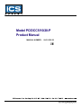
1
Model PCIDCC5/10/20-P
Product Manual
MANUAL NUMBER :
00431-550-1B
FOREWORD
This product manual provides information to install, operate and or program the referenced product(s)
manufactured or distributed by ICS Advent. The following pages contain information regarding the
warranty and repair policies.
Check our Web site (www.icsadvent.com) for technical information, manuals, and BIOS updates.
Technical assistance is also available at: 800-480-0044 (U.S.) or 858-677-0877 (international).
Customer Comments: If you experience any problems with this manual or just want to provide some
feedback, please send us a message using the online "Service Form" on our Web site (www.icsadvent.com)
under "Support." Detail any errors you find. We will correct the errors or problems as soon as possible and
post the revised manual in our online Support Library. Thank you.
The information in this document is provided for reference only. ICS Advent does not assume any liability
arising from the application or use of the information or products described herein. This document may
contain or reference information and products protected by copyrights or patents and does not convey any
license under the patent rights of ICS Advent, nor the rights of others.
Copyright © 1998, 1999, a California Corporation, 6260 Sequence Drive, San Diego, CA 92121-4371. ICS
Advent is a Registered Trademark of ICS Advent. All trademarks and registered trademarks are the property of their respective owners. All rights reserved. Printed in the United States of America. No part of this
publication may be reproduced, stored in a retrieval system, or transmitted, in any form or by any means,
electronic, mechanical, photocopying, recording , or otherwise, without the prior written permission of the
publisher.
Page - iii
This page intentionally left blank
Page - iv
Guarantee
A thirty day money-back guarantee is provided on all standard products sold. Special order products are
covered by our Limited Warranty, however they may not be returned for refund or credit. EPROMs,
RAM, Flash EPROMs or other forms of solid electronic media are not returnable for credit - but for
replacement only. Extended Warranty available. Consult factory.
Refunds
In order to receive a refund on a product for the purchase price, the product must not have been
damaged by the customer or by the common carrier chosen by the customer to return the goods and
the product must be returned complete (meaning all manuals, software, cables, etc.) within 30 days of
receipt and in an as-new and resalable condition. The Return Procedure must be followed to assure
prompt refund.
Restocking Charges
Product returned after 30 days, and before 60 days, of the purchase will be subject to a minimum 20%
restocking charge and charges for any damaged or missing parts. Products not returned within 60
days of purchase, or products which are not in an as-new and re-saleable condition, are not eligible
for credit return and will be returned to the customer.
Limited Warranty
Effective April 1, 1998, all products carry a 2-year limited warranty. Within two years of purchase,
ICS Advent will repair or replace, at our option, any defective product. ICS Advent will service the
warranty for all standard catalog products for the first two years from the date of shipment.
Please note: The 2-year warranty may not apply to special promotion items. Please consult the factory for
warranty verification.
The limited warranty is void if the product has been subjected to alteration, neglect, misuse, or abuse; if any
repairs have been attempted by anyone other than ICS Advent or its authorized agent; or if the failure is
caused by accident, acts of God, or other causes beyond the control of ICS Advent or the manufacturer.
Neglect, misuse, and abuse shall include any installation, operation, or maintenance of the product other than
in accordance with the user’s manual.
No agent, dealer, distributor, service company, or other party is authorized to change, modify, or extend the
terms of this Limited Warranty in any manner whatsoever. ICS Advent reserves the right to make changes
or improvements in any product without incurring any obligation to similarly alter products previously
purchased.
Shipments not in compliance with this Guarantee
and Limited Warranty Return Policy will not be accepted by ICS Advent.
Page - v
Return Procedure
For any Guarantee or Limited Warranty return, please contact ICS Advent's Customer Service at
800-480-0044 (U.S.) or 858-677-0877 (international) and obtain a Return Material Authorization (RMA)
Number. All product(s) returned to ICS Advent for service or credit must be accompanied by a Return
Material Authorization (RMA) Number. Freight on all returned items must be prepaid by the customer who
is responsible for any loss or damage caused by common carrier in transit. Returns for Warranty must
include a Failure Report for each unit, by serial number(s), as well as a copy of the original invoice showing
date of purchase.
To reduce risk of damage, returns of product must be in an ICS Advent shipping container. If the original
container has been lost or damaged, new shipping containers may be obtained from ICS Advent Customer
Service at a nominal cost.
ICS Advent owns all parts removed from repaired products. ICS Advent uses new and reconditioned parts
made by various manufacturers in performing warranty repairs and building replacement products.
If ICS Advent repairs or replaces a product, its warranty term is not extended.
ICS Advent will normally return your replacement or repaired items via Second Day Air. Overnight delivery
or delivery via other carriers is available at an additional charge.
Limitation of Liability
In no event shall ICS Advent be liable for any defect in hardware, software, loss, or inadequacy of data of
any kind, or for any direct, indirect, incidental, or consequential damages in connection with or arising out of
the performance or use of any product furnished hereunder. ICS Advent liability shall in no event exceed the
purchase price of the product purchased hereunder. The foregoing limitation of liability shall be equally
applicable to any service provided by ICS Advent or its authorized agent.
Some Sales Items and Customized Systems are not subject to the guarantee and limited warranty.
However in these instances , any deviations will be disclosed prior to sales and noted in the original invoice.
ICS Advent reserves the right to refuse returns or credits on software or special order items.
Page - vi
Advisories
Three types of advisories are used throughout the manual to stress important points or warn of potential
hazards to the user or the system. They are the Note, the Caution, and the Warning. Following is an example
of each type of advisory:
Note: The note is used to present special instruction, or to provide extra information which may
help to simplify the use of the product.
CAUTION!
A Caution is used to alert you to a situation which if ignored may cause injury or
damage equipment.
WARNING!
A Warning is used to alert you of a situation which if ignored will cause serious injury.
Cautions and Warnings are accented with triangular symbols. The exclamation symbol is used in all cautions
and warnings to help alert you to the important instructions. The lightning flash symbol is used on the left
hand side of a caution or a warning if the advisory relates to the presence of voltage which may be of
sufficient magnitude to cause electrical shock.
Use caution when servicing any electrical component. We have tried to identify the areas which may pose
a Caution or Warning condition in this manual; however, ICS Advent does not claim to have covered all
situations which might require the use of a Caution or Warning.
You must refer to the documentation for any component you install into a computer system to ensure proper
precautions and procedures are followed.
Page - vii
This page intentionally left blank
Page - viii
Table of Contents
Chapter 1: Introduction ............................................................................................. 1-1
Counters ............................................................................................................................................ 1-1
Timebase ........................................................................................................................................... 1-1
Digital I/O .......................................................................................................................................... 1-1
Interrupts ........................................................................................................................................... 1-2
Software ............................................................................................................................................ 1-2
Specifications .................................................................................................................................... 1-2
Chapter 2: Installation ................................................................................................ 2-1
Installation Overview ........................................................................................................................... 2-1
Installing the Board ............................................................................................................................ 2-1
Chapter 3: Programming ........................................................................................... 3-1
I/O Addresses .................................................................................................................................... 3-1
Byte-Oriented Operation .................................................................................................................... 3-3
9513 Register Functions .................................................................................................................... 3-3
Indirect Addressing ............................................................................................................................ 3-3
Programming Sequence .................................................................................................................... 3-3
Initialization Sequence ................................................................................................................ 3-4
Saving, Reading, and Disarming the Counters ............................................................................ 3-6
Master Mode Register ....................................................................................................................... 3-6
Master Mode Register Bit Assignments ...................................................................................... 3-7
Counter Mode Register ...................................................................................................................... 3-8
Counter Mode Register Bit Assignments ..................................................................................... 3-9
Data Pointer Register ........................................................................................................................ 3-9
Peek and Poke Driver for Windows 95/NT ........................................................................................ 3-11
Using The Library ....................................................................................................................... 3-12
PeekPoke Driver for Windows NT Installation .................................................................................... 3-13
Installing the Windows NT PeekPoke Driver ............................................................................... 3-13
PeekPoke Driver for Windows 95 Installation .................................................................................... 3-14
Installing the Windows 95 PeekPoke Driver ............................................................................... 3-14
Chapter 4: How to remain CE Compliant ................................................................. 4-1
How to remain CE Compliant ............................................................................................................. 4-1
FCC Compliance Statement for Class A Devices ................................................................................ 4-1
Page - ix
Chapter 5: Connector Pin Assignments ................................................................... 5-1
CE Declaration of Conformity
List of Figures
Figure 1-1: PCIDCC5-P Block Diagram .................................................................................................... 1-4
Figure 1-2: PCIDCC5-P Board Layout ..................................................................................................... 1-5
Figure 1-3: PCIDCC10-P and PCIDCC20-P Block diagram ...................................................................... 1-6
Figure 1-4: PCIDCC10-P and PCIDCC20-P Board Layout ......................................................................... 1-7
Figure 3-1: Master Mode Register Bit Assignments .................................................................................. 3-6
Figure 3-2: Counter Mode Register Bit Assignments ................................................................................ 3-8
Figure 5-1: PCIDCC5-P 37-Pin Connector ................................................................................................ 5-2
Current Revision 1B
February 2001
Page - x
Chapter 1: Introduction
Chapter 1: Introduction
The PCIDCC5/10/20-P series is a family of counter/timer cards consiting of three different models:
the PCIDCC5-P, PCIDCC10-P, and the PCIDCC20-P. The PCIDCC20-P contains four AM9513
System Timing Controller LSI circuits. Each AM9513 consits of five independant 16 bit up/down
counters. The PCIDCC10-P contains two AM9513 circuits and the PCIDCC5-P contains one. The
PCIDCC5-P does however contain an 8 bit input port and an 8 bit output port in addition to the 9513.
The PCIDCC10-P and PCIDCC20-P are physically the same board except for the difference in the
number of counters. On the PCIDCC10-P and PCIDCC20-P, the signals for each counter are
available on independant 26 pin headers; on the PCIDCC5-P, the signals are available on a DB37
male connector.
Counters
The counters can be programmed to count up or count down in either binary or BCD. A selection
of various internal and external frequency sources and outputs may be chosen as inputs for individual counters with software selectable active-high or active-low polarities. Each counter may be
gated by either software or hardware.
Each counter has associated with it a Load Register and a Hold Register. Load Registers are used
to automatically reload the counter to any predefined value, thus controlling the effective count
period.
Hold Registers are used to save count values without disturbing the count process. This permits the
processor to read intermediate counts. The Hold Register may also be used as a second Load
Register, in some modes. Counters 1 and 2 have additional alarm registers and comparators associated with them plus logic for operations in a 24-hour time-of-day mode. The time-of-day logic will
accept 50Hz, 60Hz, and 100Hz input frequencies.
Each counter has a single dedicated output pin. Considerable versatility for configuring both the input
and the gating of individual counters is provided. This not only permits dynamic re-assignment of
inputs under software control, but also allows multiple counters to use a single input, allows a single
gate input to control more than one counter, and allows for cascading.
Timebase
A 4Mhz crystal oscillator is provided on the card. It provides a 1Mhz clock input for the counters.
Digital I/O
The PCIDCC5-P also contains an 8-bit, latched, parallel digital, TTL input port and an 8 bit, latched,
parallel digital, TTL output port. The output port features tri-state outputs designed specifically for
driving capacitive or low-impedance loads. Outputs can source up to 24mA and can drive 15 standard TTL loads or 60 low-power Schottky TTL loads.
Manual 00431-550-1
Page 1-1
PCIDCC5/10/20-P Manual
Interrupts
Interrupts from counter outputs or external sources are supported. The Interrupt Request Level
(IRQ) is selected by the PCI compatiable BIOS. Each slot on the PCI motherboard is assigned one
IRQ. If a conflict arises from the IRQ selected by the BIOS, simply move the PCIDCC5/10/20-P to
a different slot. On the PCIDCC5-P, if an Interrupt Enable input at I/O connector pin 2 is held high,
the interrupt function is disabled. Conversely, if the Interrupt Enable input is held low, a rising edge
on the Interrupt Input, pin 1, will generate an interrupt on the selected level. It is the user’s responsibility to set up and enable the Programmable Interrupt Controller (PCI), the interrupt vectors, and
an interrupt service routine.
Typically, counter outputs can be jumpered to the Interrupt Input and the Interrupt Enable can be
controlled by one of the digital output bits. This allows software control of a periodic interrupt, for
example.
Software
The files contained on the provided diskette may be copied onto your hard disk. Files contained on
the disk are stored in separate directories. Refer to the README.TXT file on the diskette for more
information about these files.
Specifications
Sample Modes for the 9513 Timer
Software-Triggered Strobe w/No Hardware Gating
Software-Triggered Strobe w/Level Gating
Hardware-Triggered Strobe
Rate Generator w/Synchronization (Event Counter with Auto-Read/Reset)
Rate Generator w/No Hardware Gating
Rate Generator w/Level Gating
Retriggerable One-Shot
Non-Retriggerable One-Shot
Hardware-Triggered Delayed-Pulse One-Shot
Hardware-Triggered Delayed Pulse Strobe
Software-Triggered Delayed-Pulse One-Shot
Software-Triggered Delayed-Pulse One-Shot w/ Hardware Gating
Variable Duty Cycle Rate Generator w/No Hardware Gating
Variable Duty Cycle Rate Generator w/Level Gating
Software-Triggered Strobe w/Level Gating and Hardware Retriggering
Software-Triggered Strobe w/Edge gating and Hardware Retriggering
Frequency Shift Keying
Page 1-2
Manual 00431-550-1
Chapter 1: Introduction
Inputs
Voltage: One LSTTL load
Logic High:
2.0 to 5.0 VDC
Logic Low:
-0.5 to 0.8 VDC
Hysteresis (Source & Gate):
0.2V min., 0.3V typical
Switching Characteristics:
See Appendix A
Maximum Input Frequency:
7 MHz
Outputs
Counter Outputs: Can sink 3.2 mA and source 200 uA
Fout: Can sink 3.2 mA and source 200 uA.
Digital Output Port (PCI/DCC5-P Only): Can drive up to 15 standard TTL loads or 60 low-power
Schottky loads.
Enviromental
Operating Temperature Range:
0 to 50o C.
Storage Temperature Range:
-25 to +85o C.
Humidity:
0 to 90% RH, non-condensing
Power Required:
5 VDC at 400 mA typical
Agency Approvals
CE Conformity with:
EU EMC Directive 89/336/EEC
EU Low Voltage Directive 72/23/EEC
Manual 00431-550-1
Page 1-3
PCIDCC5/10/20-P Manual
AMD 9513
4 MHZ OSCILLATOR
AND
DIVIDE BY 4
CIRCUITRY
1 MHZ
STROBE
INPUT
PORT
(8-BIT
DATA
LATCH)
ENABLE
INTERRUPT
PROGRAMMABLE
DIVIDER
OUT
#1 16 BIT
UP/DOWN
COUNTER
IN
GATE
OUT
#2 16 BIT
UP/DOWN
COUNTER
IN
GATE
OUT
#3 16 BIT
UP/DOWN
COUNTER
IN
GATE
OUT
#4 16 BIT
UP/DOWN
COUNTER
IN
GATE
OUT
#5 16 BIT
UP/DOWN
COUNTER
IN
GATE
OUT
DATA BUS
EPLD FOR IRQ
DIGITAL I/O OUTPUT PORT
AND
PCI INTERFACE
ADDRESS
IRQ
DATA
PCI BUS
Figure 1-1: PCIDCC5-P Block Diagram
Page 1-4
Manual 00431-550-1
Chapter 1: Introduction
Figure 1-2: PCIDCC5-P Board Layout
Manual 00431-550-1
Page 1-5
PCIDCC5/10/20-P Manual
4 MHZ OSCILLATOR
AND
DIVIDE BY 4
CIRCUITRY
1 MHZ
PCI/DCC20 ONLY
AMD 9513
AMD 9513
AMD 9513
AMD 9513
PROGRAMMABLE
DIVIDER
OUT
PROGRAMMABLE
DIVIDER
OUT
PROGRAMMABLE
DIVIDER
OUT
PROGRAMMABLE
DIVIDER
OUT
#1 16 BIT
UP/DOWN
COUNTER
IN
GATE
OUT
#1 16 BIT
UP/DOWN
COUNTER
IN
GATE
OUT
#1 16 BIT
UP/DOWN
COUNTER
IN
GATE
OUT
#1 16 BIT
UP/DOWN
COUNTER
IN
GATE
OUT
#2 16 BIT
UP/DOWN
COUNTER
IN
GATE
OUT
#2 16 BIT
UP/DOWN
COUNTER
IN
GATE
OUT
#2 16 BIT
UP/DOWN
COUNTER
IN
GATE
OUT
#2 16 BIT
UP/DOWN
COUNTER
IN
GATE
OUT
#3 16 BIT
UP/DOWN
COUNTER
IN
GATE
OUT
#3 16 BIT
UP/DOWN
COUNTER
IN
GATE
OUT
#3 16 BIT
UP/DOWN
COUNTER
IN
GATE
OUT
#3 16 BIT
UP/DOWN
COUNTER
IN
GATE
OUT
#4 16 BIT
UP/DOWN
COUNTER
IN
GATE
OUT
#4 16 BIT
UP/DOWN
COUNTER
IN
GATE
OUT
#4 16 BIT
UP/DOWN
COUNTER
IN
GATE
OUT
#4 16 BIT
UP/DOWN
COUNTER
IN
GATE
OUT
#5 16 BIT
UP/DOWN
COUNTER
IN
GATE
OUT
#5 16 BIT
UP/DOWN
COUNTER
IN
GATE
OUT
#5 16 BIT
UP/DOWN
COUNTER
IN
GATE
OUT
#5 16 BIT
UP/DOWN
COUNTER
IN
GATE
OUT
DATA BUS
EPLD FOR IRQ
DIGITAL I/O OUTPUT PORT
AND
PCI INTERFACE
ADDRESS
IRQ
OPTIONAL INTERRUPT FROM
CHIP#1, COUNTER#5
DATA
PCI BUS
Figure 1-3: PCIDCC10-P and PCIDCC20-P Block diagram
Page 1-6
Manual 00431-550-1
U2
U3
U4
DCC 20 ONLY
U1
DCC 20 ONLY
Chapter 1: Introduction
J1
J2
J3
J4
Figure 1-4: PCIDCC10-P and PCIDCC20-P Board Layout
Manual 00431-550-1
Page 1-7
Chapter 2: Installation
Chapter 2: Installation
Installation Overview
The PCIDCC5/10/20-P series of adapters is fully PCI 2.1 compliant and thus 'Plug-and-Play'. The
Interrupt Request (IRQ) and Base Address of the adapter is defined by the PCI BIOS. This scheme
typically prevents I/O and IRQ conflicts. As with any scheme however, coflicts may occur. If a
conflict does occur, simply move the adapter to a different PCI slot. Each slot is assigned a specific
I/O range and IRQ, so moving slots typically resolves any conflict.
.
Installing the Board
CAUTION!
Be sure to turn off the power to the computer before installing the board. Failure to
do so could cause damage to the board or computer, invalidating the warranty
To install the board, perform the following steps:
1. Turn off the computer and remove the cover of the case.
2. Select an empty, PCI slot and remove the screw at the top of the slot’s backplate.
3. Remove the backplate.
4. Plug the board into the empty slot. Ensure that the board is firmly seated in the slot.
5. Reinstall the screw removed in step 2. Ensure that the board is securely fastened in place.
6. Reinstall the cover of the case.
Manual 00431-550-1
Page 2-1
Chapter 3: Programming
Chapter 3: Programming
I/O Addresses
The PCIDCC5-P, PCIDCC10-P, and PCIDCC20-P sixteen consecutive addresses in the I/O space.
The base or starting address is selected by the PCI BIOS and falls on a 16-bit boundary. The
address maps for the appropriate boards are as follows:
PCIDCC5-P
I/O Addre s s
Write
R e ad
Base + 0
9513 Data Write
9513 Data Read
Base + 1
9513 Command
9513 Status
Base + 2
invalid
Digital Input IP0- 7
Base + 3
Digital Output OP0- 7
invalid
Base + 4- 7
not used
not used
Base +8
not used
Interrupt Status - rising edge
latched
1 = IRQ pending
0 = no IRQ
Interrupt source:
PCIDCC5- P = DB37 Pin1
PCIDCC10- P & 20- P = Out5 of
connector J1
Base + 9
Bit D0
Register Interrupt
Enable
0 = IRQ Disabled
1 = IRQ Enabled
after reset = 0
Bit D0
Register Interrupt Enable
0 = IRQ Disabled
1 = IRQ Enabled
after reset = 0
Manual 00431-550-1
Page 3-1
PCIDCC5/10/20-P Manual
PCIDCC10-P & 20-P
Chip
I/O Addre s s
Write
R e ad
1
Base + 0
9513 Data Write
9513 Data Read
Base + 1
9513 Command
9513 Status
Base + 2
9513 Data Write
9513 Data Read
Base + 3
9513 Command
9513 Status
2
PCIDCC20-P
3
4
Base + 4
9513 Data Write
9513 Data Read
Base + 5
9513 Command
9513 Status
Base + 6
9513 Data Write
9513 Data Read
Base + 7
9513 Command
9513 Status
Exte nde d Re gis te rs
Page 3-2
Base + 8
not used
Interrupt Status - rising
edge latched
1 = IRQ pending
0 = no IRQ
Interrupt source:
PCIDCC5- P = DB37
Pin1
PCIDCC10- P & 20- P = Out5 of
connector J1
Base + 9
Bit D0
Register Interrupt
Enable
0 = IRQ Disabled
1 = IRQ Enabled
after reset = 0
Bit D0
Register Interrupt
Enable
0 = IRQ Disabled
1 = IRQ Enabled
after reset = 0
Manual 00431-550-1
Chapter 3: Programming
Byte-Oriented Operation
If you are using an AT class computer, note that all ports are eight bits wide (one byte) and you
should perform byte-oriented read/write operations rather than word (16 bits) operations. When
performing consecutive byte transfers to the same I/O port on an AT, be sure to allow sufficient
recovery time for the I/O circuits.
9513 Register Functions
All data transfers to the 9513 LSI counter timer chip are performed through two I/O ports. Since
there are a number of internal registers in the 9513 LSI chip, an indirect system of accessing those
registers is used via an internal data pointer register which, in turn, is reached through the command
register. The Data port (Base +0) is used for data transfer; i.e., loading and reading registers. The
Command port (Base +1) is used for addressing registers. The Command port also performs other
functions such as loading and enabling the counters, latching counter contents, etc. (Appendix A of
this manual contains a data sheet with detailed information on the 9513 LSI chip.)
Indirect Addressing
The basic premise behind indirect addressing is to first point to the register you wish to access. To do
this, you use the data pointer register which is one of several specific uses for the Command port
(Base +1). Then you load or read the data via 2 writes or reads to the Data port (Base +0). Because
of this, most functions require at least three lines of code. To simplify programming slightly, the 9513
also uses the Command port (Base +1) to perform other frequently used commands with a single
write. This is explained further in the following programming section.
Programming Sequence
Setup and initialization of this board follows a very basic procedure. The necessary steps and code
examples that follow outline this procedure. The various registers and bit definitions on the following
pages can be modified for use in your own application.
Doing a Master Reset to the board, before the initialization sequence, is a good idea. Write "FF" to
the Command Register of each chip before initializing the board.{1st chip base+1, 2nd chip base+3}.
It is not always necessary to do a Master Reset but some operating systems require it.
In the following steps, delays have not been added. Whenever two OUT statements follow one
another in a compiled language, a delay must be added between them to allow for hardware
recovery time. To insert a delay, simply use an empty loop as follows:
For X= 1 to 2: Next X
Manual 00431-550-1
Page 3-3
PCIDCC5/10/20-P Manual
Initialization Sequence
1. Set the Master Mode (MM) register. This initializes the board. Refer to the Master Mode Register
section later in this chapter for bit definitions for this register.
OUT
BASEADDR+1,
&H17
'Write to Data Pointer Register to point to the
'Master Mode Register.
OUT
BASEADDR,
&HB0
'Load LSB of MM register.
OUT
BASEADDR,
&H40
'Load MSB of MM register.
This particular example sets the board in the following configuration:
-Binary scalar division
-Data Pointer Increment disabled
-8 bit bus (always)
-Fout active
-Fout = Fout source/16
-Compare & Time-of-Day disabled
2. Set Counter Mode (CM) register for each counter. Refer to the Counter Mode Register section
later in this chapter for bit definitions for this register.
OUT
BASEADDR+1,
&H01
OUT
BASEADDR,
&H22
'Load LSB of CM1 register.
OUT
BASEADDR,
&H01
'Load MSB of CM1 register.
OUT
BASEADDR+1,
OUT
BASEADDR,
&H00
'Load LSB of CM2 register.
OUT
BASEADDR,
&H22
'Load MSB of CM2 register.
&H02
'Point to the Counter 1 Mode Register (CM1).
'Point to Counter Mode Register (CM2).
This sets the counters (1 and 2) to the following modes:
Counter 1:
-No gating (special gate disabled)
-Count on rising edge
-Counter source from SRC1 pin
-Reload from load register
-Count repetitively
-Count binary
-Count down
-Toggle output on terminal count
Page 3-4
Manual 00431-550-1
Chapter 3: Programming
Counter 2:
s-No gating
-Count on rising edge
-Counter source is output of Counter 1
-Reload from load register
-Count repetitively
-Count in binary
-Count down
-Toggle output on terminal count
3. Fill each Counter Load Register with a starting value (which is automatically reloaded into the
counter after each terminal count.)
OUT BASEADDR+1, &H09
'Point to the Counter 1 Load Register.
OUT BASEADDR, &HFF
'Load LSB of C1 Load Register.
OUT BASEADDR, &HFF
'Load MSB of C1 Load Register.
OUT BASEADDR, &H0A
'Point to Counter 2 Load Register.
OUT BASEADDR, &H00
'Load LSB of C2 Load Register.
OUT
'Load MSB of C2 Load Register.
BASEADDR,
&H80
4. Load counters (transfer contents of load register into counter). See the Command description
section later in this chapter for more information on using this command.
OUT
BASEADDR+1,
&H43
'Loads Counter 1 and 2.
5. Arm counters (this begins the count cycle.)
OUT
BASEADDR+1,
&H21
'Arms counter 1.
OUT
BASEADDR+1,
&H22
'Arms counter 2.
Note: To arm both counters simultaneously, use OUT BASEADDR+1, &H23.
Manual 00431-550-1
Page 3-5
PCIDCC5/10/20-P Manual
Saving, Reading, and Disarming the Counters
1. Save the count (put the current count into the Counter Hold Register while counting continues
undisturbed):
OUT
BASEADDR+1,
&HA3
'Saves counter 1 and 2.
2. Read the count from the Counter Hold Register:
3.
OUT BASEADDR+1, &H11
'Point to Counter 1 Hold Register.
CTR1LO=INP(BASEADDR)
'Read the LSB.
CTR1HI=INP(BASEADDR)
'Read the MSB.
OUT BASEADDR+1, &H12
'Point to Counter 2 Hold Register.
CTR2LO=INP(BASEADDR)
'Read the LSB.
CTR2HI=INP(BASEADDR)
'Read the MSB.
Disarm counters when done.
OUT
BASEADDR+1,
&HC1
'Disarms
counter
1.
OUT
BASEADDR+1,
&HC2
'Disarms
counter
2.
Master Mode Register
The 16-bit Master Mode (MM) register controls the overall operation of the board and should be
initialized by your program. It is a 16-bit register and, in the following description, bit locations are
listed as MM15 through MM0 which correspond to the most significant bit through the least significant bit.
(fig3-1.wmf) (updated manual copy)
Figure 3-1: Master Mode Register Bit Assignments
Page 3-6
Manual 00431-550-1
Chapter 3: Programming
Master Mode Register Bit Assignments
Function
Properties
Scaler Ratios
Master Mode bit MM15 controls the counting configuration of the Frequency
Scaler counter. When MM15 = 0, the Scaler divides the oscillator frequency
in binary steps so that each subfrequency is 1/16 of the preceding frequency.
When MM15 = 1, the Scaler divides in BCD steps so that adjacent
frequencies are related by ratios of 10 instead of 16.
Data Pointer
Bit MM14 controls the Data Pointer Logic to enable or disable the
sequencing automatic, sequencing functions. When MM14 = 1, the contents
of the Data Pointer can be changed only directly by entering a command.
When MM14 = 0, several types of automatic sequencing of the Data Pointer
are available. These are described in the Data Pointer register section of the
data sheet at the back of this manual.
Bus Width
Bit MM13 controls the multiplexer at the data bus interface in order to
configure the part for an 8-bit or 16-bit external bus. The PCI/DCC-P Series
uses an 8-bit bus.
FOUT Gate
Master Mode bit MM12 provides a software gating capability for the FOUT
signal. When MM12 = 1, FOUT is off and in a low-impedance state to the
ground.
FOUT Divider
Bits MM8 through MM1 specify the dividing ratio for the FOUT Divider. The
FOUT source (selected bye bits MM4 through MM7) is divided by an integer
value between 1 and 16, inclusive, and is then passed to the FOUT output
buffer.
FOUT Source
Master Mode bits MM4 through MM7 specify the source input for the FOUT
divider. Fifteen inputs are available for selection and they include the five
Source pins, the five Gate pins and the five internal frequencies derived from
the oscillator and the scaler.
Comparator Enable Bits MM2 and MM3 control the Comparator associated with the Controllers
1 and 2. When a Comparator is enabled, its output is substituted for the normal
counter output on the associated OUT1 or OUT2 pin. See the data sheet at
the back of this manual for more information.
Time-of-Day
Manual 00431-550-1
Bits MM0 and MM1 of the Master Mode register specify the Time-of-Day
(TOD) options. When MM0 = 0 and MM1 = 0, the special logic used to
implement the TOD is disabled and Counter 1 and 2 will operate in exactly
the same way as Counter 3, 4, and 5. When MM0 =1 or MM1 = 1, additional
counter decoding and control logic is enabled on Counters 1 and 2, which
causes their decades to turn over at the counts that generate appropriate 24hour TOD accumulations. For additional information, see the Time-of-Day
chapter in the 9513A System timing controller technical manual.
Page 3-7
PCIDCC5/10/20-P Manual
Counter Mode Register
The Counter Mode register for each counter should be initialized after the Master Mode register.
The Counter Mode registers are 16-bit registers and the bit locations are designated CM15 through
CM0, which correspond to the most significant bit to the least significant bit. Each Counter uses a
separate Counter Mode (CM) register allowing the individual counters to operate independently.
These options include output configuration, count control, count source and gating control. The
following figure shows the bit assignments for the Counter Mode registers. This section describes
the control options in detail. Note that generally each counter is independently configured and does
not depend on modes of other counters. The Counter Mode register should be loaded only when the
counter is Disarmed. Attempts to load the Counter Mode register when the counter is armed may
result in erratic counter operation.
(fig3-2.wmf)(modified in manual)
Figure 3-2: Counter Mode Register Bit Assignments
Page 3-8
Manual 00431-550-1
Chapter 3: Programming
Counter Mode Register Bit Assignments
Function
Properties
Gating Control:
Counter Mode bits CM15, CM14, and CM13 specify the hardware gating
options. When “no gating” is selected (000), the counter will proceed
unconditionally as long as it is armed. For any other gating mode, the count
process is conditioned by the specified gating configuration.
Counter Source
Selection:
Counter Mode bits CM8 through CM12 specify the source used as input to
the counter and the active edge that is counted. Bit CM12 controls the polarity
for all the sources; logic zero counts rising edges and logic one counts falling
edges. Bits CM8 through CM11 select 1 of 16 counting sources to route to
the counter input. Five of the available inputs are internal frequencies
derived from the internal oscillator. Ten of the available inputs are interface
pins; five are labeled SRC and five are labeled GATE. The 16th available
input is the TC output from the adjacent lower-numbered counter. (The
Counter 5 TC wraps around to the Counter 1 input.)
Count Control:
Counter Mode bits CM3 through CM7 specify the various options available
for direct control of the counting process. CM3 and CM4 operate independently
of the others and control up/down and BCD/binary counting. Bit CM5 controls
the repetitions of the count process. When CM5 = 1, counting will proceed
in the specified mode until the counter is disarmed. When CM5 = 0, the count
process will proceed only until one full cycle of operation occurs. This may
occur after one or two TC events. Bit CM7 controls the special gating functions
that allow retriggering and the selection of Load or Hold sources for counter
reloading.
Output Control:
Counter mode bits CM0 through CM2 specify the output control configuration.
The OUT pin may be off (a high impedance state), or it may be inactive with
a low-impedance to ground. The three remaining valid combinations represent
the active-high, active-low, or TC toggle output waveforms.
Data Pointer Register
The Data Pointer Register is set using the information in the following figure. For detailed information about the Data Pointer Register, refer to the data sheet at the back of this manual. As discussed
in the Programming Sequence Section of this chapter, this register points to other registers in the
9513. It navigates through the various registers of the 9513’s indirect addressing scheme. The Data
Pointer Register is selected with a write to Base +1 where the three most significant bits must be 000.
Command Port (Base +1)
The Command port of the 9513 has many different functions, including loading, arming, and saving
the counters. It also allows access to the counter registers via the Data Pointer Register. The
various functions are indicated by the three most significant bits.
(fig3-3.wmf) (updated manual copy)
Manual 00431-550-1
Page 3-9
PCIDCC5/10/20-P Manual
Command Descriptions (BASE+1)
Six of the command types are used for direct software control of the counting process and they
each contain a 5-bit S field. In a linear-select fashion, each bit in the S field corresponds to one of
five general counters (S1=Counter 1, S2=Counter2, etc.). When an S bit is a one, the specified
operation is performed on the counter so designated; when an S bit is a zero, no operation occurs for
the corresponding counter.
Arm Counters
C7
C6
C5
C4
C3
C2
C1
C0
0
0
1
S5
S4
S3
S2
S1
Any combination of counters, as specified by the S field, will be enabled for counting. A counter
must be armed before counting can commence. Once armed, the counting process may be further
enabled or disabled using the hardware gating facilities.
Load Counters
C7
C6
C5
C4
C3
C2
C1
C0
0
1
0
S5
S4
S3
S2
S1
Any combination of counters, as specified in the S field, will be loaded with previously entered
values. The source of information for each counter will be either the Load register or the Hold
register, as determined by the operating configuration in the Mode register.
Load and Arm Counters
C7
C6
C5
C4
C3
C2
C1
C0
0
1
1
S5
S4
S3
S2
S1
Any combination of counters, as specified in the S field, will be first loaded then armed. This command is equivalent to issuing a LOAD command and then ARM command.
Page 3-10
Manual 00431-550-1
Chapter 3: Programming
Disarm Counters
C7
C6
C5
C4
C3
C2
C1
C0
1
1
0
S5
S4
S3
S2
S1
Any combination of counters, as specified by the S field, will be disabled from counting. A disarmed
counter will cease all counting independent of other conditions.
Save Counters
C7
C6
C5
C4
C3
C2
C1
C0
1
0
1
S5
S4
S3
S2
S1
Any combination of counters, as specified by the S field, will have their contents transferred into
their associated Hold register. The transfer takes place without interfering with any counting that may
be underway. This command will overwrite any previous Hold register contents.
Disarm and Save Counters
C7
C6
C5
C4
C3
C2
C1
C0
1
0
0
S5
S4
S3
S2
S1
Any combination of counters, as specified by the S field, will be disarmed and the contents of the
Counter register will be transferred into the associated Hold registers.
Master Reset
C7
C6
C5
C4
C3
C2
C1
C0
1
1
1
1
1
1
1
1
The Master Reset command duplicates the action of the power-on reset circuitry. It disarms all
counters, enters Hex 0000 in the Master Mode, Load and Hold registers and enter 0B00 hex in each
of the Counter Mode Registers. Doing a Master Reset to the board, before the initialization sequence,
is a good idea. Write "FF" to the Command Register of each chip before initializing the board. {1st
chip base+1, 2nd chip base+3}. It is not always necessary to do a Master Reset but some operating
systems require it.
Peek and Poke Driver for Windows 95/NT
This driver allows developers to write Win32 programs which access hardware I/O ports and physical memory. This should allow easier testing of hardware components since they can be accessed
without the use of a specific driver.
It should be noted that this driver will give application level access to areas of the hardware and
memory which can quite easily crash the operating system or even corrupt data. Care needs to be
taken to only access known memory or I/O ports.
Manual 00431-550-1
Page 3-11
PCIDCC5/10/20-P Manual
Using The Library
There are two libraries that can be used to ease use of the Peek and Poke driver. They are
pplib95.lib and pplibnt.lib. They are used for Windows 95 and Windows NT respectively. These
libraries provide I/O routines familiar to those who have used Microsoft compilers in the past.
To use a library, add pplib95.lib or pplibnt.lib to your link, whichever is appropriate for the target OS.
Include pplib95.h or pplibnt.h in the C/C++ file you will be accessing the functions from. These
libraries are compatible with all Microsoft compilers. NOTE: These libraries are not thread safe.
The following is a list of the functions provided by the library.
Function
Description
BOOL ics_pp_open ( void )
Opens the Peek and Poke driver. Returns TRUE if successful. This
must be called before any calls are made to the other library
functions.
void ics_pp_close ( void )
Closes the driver. Should be called before the application exits.
void *ics_pp_make_pointer
(int page, int length)
This function is used to allow access to a particular region of
physical memory by a Win32 application. page is the starting page
of the physical memory. length is the size of the region in pages.
For example, for a pointer to a region of physical memory starting
at 0xA0000 and 64k long: void *ptr = ics_pp_make_pointer (0xA0,
0x10); The pointer can then be treated as a standard C/C++ pointer.
NOTE: Be sure to release this memory region back to the system
with a call to ics_pp_release_pointer. (See Below.)
void ics_pp_release_pointer
(void *address, int length)
This function is used to release a memory mapping made with
ics_pp_make_pointer. It is important to release such pointers back
to the system. Failure to do so could affect the way the system
runs even after the application has exited. address is the address
that was returned by the ics_pp_make_pointer function. length is
the size of the mapped region in pages.
int _outp (USHORT port,
int data) USHORT _outpw
(USHORT port, USHORT
data) ULONG _outpl
(USHORT port, ULONG
data)
These functions output data to the given port. Use _outp for byte
width, _outpw for word width, and _outpl for double word width.
Int _inp (USHORT port)
USHORT _inpw (USHORT
port) ULONG _inpl
(USHORT port)
These functions return data input from the given port. Use _inp for
byte width, _inpw for word width, and _inpl for double word width.
Page 3-12
Manual 00431-550-1
Chapter 3: Programming
PeekPoke Driver for Windows NT Installation
This driver allows developers to write WinNT programs which access hardware I/O ports and
physical memory.
Installing the Windows NT PeekPoke Driver
Under Windows NT 3.51:
•
From the Program Manager, click on File->Run.
•
Type a:\setup and press OK.
From Windows NT 4.0
•
From the Start Menu, select Run.
•
Type a:\setup and press OK.
The InstallShield installer will initialize and run. Follow the on-screen instructions. You will need to
provide one piece of information:
•
The destination path for the driver files.
When the files are transferred, you will be asked if you want to reboot the computer. The drivers will
not work until after a reboot.
Manual 00431-550-1
Page 3-13
PCIDCC5/10/20-P Manual
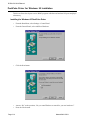
PeekPoke Driver for Windows 95 Installation
This driver allows developers to write Win95 programs which access hardware I/O ports and physical memory.
Installing the Windows 95 PeekPoke Driver
•
From the Start Menu, select Settings->Control Panel.
•
From the Control Panel, select Add New Hardware.
•
Click the Next button.
•
Answer “No” to the question, “Do you want Windows to search for you new hardware?”
•
Press the Next button.
Page 3-14
Manual 00431-550-1
Chapter 3: Programming
•
Scroll the hardware types list down and select the “System devices” type.
•
Press the Next button.
•
Press the Have Disk button.
•
Insert your disk labeled “Windows 95 PeekPoke Driver Disk.”
•
Make sure “A:\” is selected as the source.
•
Press OK.
Manual 00431-550-1
Page 3-15
PCIDCC5/10/20-P Manual
•
The model “PeekPoke – Direct Hardware Access Driver” should be selected in the Models box.
•
Press the Next button.
•
Windows 95 will copy the driver’s files onto your system.
•
Press the Finish button.
•
At this point, you will need to shutdown and reboot your machine for the changes to take effect.
Page 3-16
Manual 00431-550-1
Chapter 4: Calibration
Chapter 4: How to remain CE Compliant
How to remain CE Compliant
In order for machines to remain CE compliant, only CE compliant parts may be used. To keep a
chassis compliant it must contain only compliant cards, and for cards to remain compliant they must
be used in compliant chassis. Any modifications made to the equipment may affect the CE compliance standards and should not be done unless approved in writing by Industrial Computer Source.
The PCIDCC5/10/20-P Family is designed to be CE Compliant when used in an CE compliant
chassis. Maintaining CE Compliance also requires proper cabling and termination techniques. The
user is advised to follow proper cabling techniques from sensor to interface to ensure a complete CE
Compliant system. Industrial Computer Source does not offer engineering services for designing
cabling or termination systems. Although Industrial Computer Source offers accessory cables and
termination panels, it is the user's responsibility to ensure they are installed with proper shielding to
maintain CE compliance.
FCC Compliance Statement for Class A Devices
This device complies with Part 15 of the FCC Rules. Operation is subject to the following two
conditions:
1. This device may not cause harmful interference, and
2. This device must accept any interference received, including interference that may cause
undesired operation.
This equipment has been tested and found to comply with the limits for a Class A digital device,
pursuant to Part 15 of the FCC Rules. These limits are designed to provide reasonable protection
against harmful interference when the equipment is operated in a commercial environment. This
equipment generatesm usesm and radiates radio frequency energy and, if not installed and used in
accordance with the instructions, may cause harmful interference to radio communications. Operation of this equipment in a residential area is likely to cause harmful interference, in which case the
user will be required to correct the interference at his or her own expense.
Changes or modifications not expressly approved by the party responsible for compliance could void
the user's authority to operate the equipment.
Note: The assembler of a personal computer system may be required to test the system and/or
make necessary modifications if a system is found to cause harmful interference or to be
non-compliant with the appropriate standards for its intended use.
Manual 00431-550-1
Page 4-1
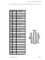
Chapter 5: Connector Pin Assignments
Chapter 5: Connector Pin Assignments
Counter and digital I/O signals are connected to the PCIDCC5-P card via a 37-pin D type connector that extends through the back of the computer case. The mating connector is an AMP 7473041 or equivalent. Pin assignments are as follows:
(37-pinA.tbl & 37-pinb.tbl)
Pin
Name
Function
1
Interrupt Input
2
(not) Interrrupt Enable
3
OP7
Digital Output Bit 7
4
OP6
Digital Output Bit 6
5
OP5
Digital Output Bit 5
6
OP4
Digital Output Bit 4
7
OP3
Digital Output Bit 3
8
OP2
Digital Output Bit 2
9
OP1
Digital Output Bit 1
10
OP0
Digital Output Bit 0
11
GND
Digital Common
12
GATE5
Counter 5 Gate
13
SRC5
Counter 5 Input
14
GATE4
Counter 4 Gate
15
SRC4
Counter 4 Input
16
GATE3
Counter 3 Gate
17
SRC3
Counter 3 Input
18
GATE2
Counter 2 Gate
19
SRC2
Counter 2 Input
Pin
Name
19
SRC2
20
+5VDC
21
Function
Counter 2 Input
+5 Volt Power (from
computer)
(not) IP Strobe
22
IP7
Digital Input 7
23
IP6
Digital Input 6
24
IP5
Digital Input 5
25
IP4
Digital Input 4
26
IP3
Digital Input 3
27
IP2
Digital Input 2
28
IP1
Digital Input 1
29
IP0
Digital Input 0
30
FOUT
Oscillator Out
31
OUT5
Counter 5 Output
32
OUT4
Counter 4 Output
33
OUT3
Counter 3 Output
34
OUT2
Counter 2 Output
35
OUT1
Counter 1 Output
36
SRC1
Counter 1 Input
37
GATE1
Counter 1 Gate
(00224.wmf)
Manual 00431-550-1
Page 5-1
PCIDCC5/10/20-P Manual
REAR VIEW
COUNTER 2 INPUT
19
37
COUNTER 1 GATE
COUNTER 2 GATE
COUNTER 1 INPUT
COUNTER 3 INPUT
COUNTER 1 OUTPUT
COUNTER 3 GATE
COUNTER 2 OUTPUT
COUNTER 4 INPUT
COUNTER 3 OUTPUT
COUNTER 4 GATE
COUNTER 4 OUTPUT
COUNTER 5 INPUT
COUNTER 5 OUTPUT
COUNTER 5 GATE
FOUT
GND
IP0
OP0
IP1
OP1
IP2
OP2
IP3
OP3
DIGITAL INPUTS
DIGITAL OUTPUTS
IP4
OP4
IP5
OP5
IP6
OP6
IP7
OP7
IP STROBE/
INTERRUPT ENABLE/
20
INTERRUPT ENABLE
+5VDC
1
Figure 5-1: PCIDCC5-P 37-Pin Connector
Page 5-2
Manual 00431-550-1
Chapter 5: Connector Pin Assignments
Counter and digital I/O signals are connected to the PCIDCC10-P & 20-P via a 26 Pin Connector.
(26-pin.tbl & 00223.wmf)
Pin
Name
Function
1
OUT3
Digital Output Bit 3
2
OUT2
Digital Output Bit 2
3
GATE2
Counter 2 Gate
4
OUT1
Digital Output Bit 1
5
OUT4
Digital Output Bit 4
6
GATE1
Counter 1 Gate
7
OUT5
Digital Output Bit 5
8
GATE3
Counter 3 Gate
9
GATE4
Counter 4 Gate
10
GATE5
Counter 5 Gate
11
SOURCE1 Counter 1 Input
12
SOURCE2 Counter 2 Input
13
SOURCE3 Counter 3 Input
14
SOURCE4 Counter 4 Input
15
SOURCE5 Counter 5 Input
16
FOUT
17
N/C
18
N/C
19
N/C
20
N/C
21
N/C
22
N/C
23
N/C
24
+5VDC
25
GND
26
N/C
Frequency Output
+5 Volt Power (ref. only)
Ground
Manual 00431-550-1
Page 5-3
Declaration of Conformity
Information Technology Equipment
6260 Sequence Drive
San Diego, CA 92121-4371
(800) 523-2320 / (858) 677-0877
The product(s) covered by this declaration:
PCIDCC5-P
PCIDCC10-P
PCIDCC20-P
The European Union directives covered by this declaration:
EMC Directive 89/336/EEC and Low Voltage Directive 73/23/EEC
The basis on which conformity is declared:
EN 50081-1:1992 Emissions, Generic Requirements
-EN 55022:1998 Limits and Methods of Measurement of Radio Disturbance Characteristics of Information
Technology Equipment
EN 50082-1:1992 Immunity, Generic Requirements
-EN61000-4-2:1995 Electrostatic Discharge (ESD) Immunity
-EN61000-4-3:1995 Radiated RF Field Immunity
-EN61000-4-4:1995 EFT Immunity for AC and I/O Lines
EN 60950:1992 Safety of Information Technology Equipment
The technical documentation required to demonstrate this product meets the requirements of the EMC Directive and the Low
Voltage Directive has been compiled by ICS Advent and is available for inspection by the relevant enforcement authorities.
Attention
The attention of the specifier, purchaser, installer, or user is drawn to special measures and limitations for use which must be
observed when the product is taken into service to maintain compliance with the above
directives. Details of these special measures and limitations are in the product manual.
Mr. Jim Jameson
President & Chief Executive Officer
ICS Advent Europe
Ben Turner Industrial Road
Oving Road
Chichester, West Sussex
PO19 4ET, UK