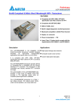
1
aTCA-RN720 Rear Transition Module with two QSFP and four SFP+ service ports. Users Guide Manual Revision: Revision Date: Part Number: 1.00 November 6, 2013 50-1G031-1000 Advance Technologies; Automate the World. aTCA-RN720 User's Guide Revision History Version Number 1.00 Dates 6/11/2013 Description Initial release 2 aTCA-RN720 User's Guide Preface Copyright 2013 ADLINK Technology, Inc. This document contains proprietary information protected by copyright. All rights are reserved. No part of this manual may be reproduced by any mechanical, electronic, or other means in any form without prior written permission of the manufacturer. Disclaimer The information in this document is subject to change without prior notice in order to improve reliability, design, and function and does not represent a commitment on the part of the manufacturer. In no event will the manufacturer be liable for direct, indirect, special, incidental, or consequential damages arising out of the use or inability to use the product or documentation, even if advised of the possibility of such damages. Environmental Responsibility ADLINK is committed to fulfill its social responsibility to global environmental preservation through compliance with the European Union's Restriction of Hazardous Substances (RoHS) directive and Waste Electrical and Electronic Equipment (WEEE) directive. Environmental protection is a top priority for ADLINK. We have enforced measures to ensure that our products, manufacturing processes, components, and raw materials have as little impact on the environment as possible. When products are at their end of life, our customers are encouraged to dispose of them in accordance with the product disposal and/or recovery programs prescribed by their nation or company. Trademarks Product names mentioned herein are used for identification purposes only and may be trademarks and/or registered trademarks of their respective companies. 3 aTCA-RN720 User's Guide Table of Contents 1 Introduction ............................................................................................................ 9 2 Summary of Specifications ................................................................................. 10 3 External Interfaces ............................................................................................... 11 3.1 3.2 3.3 3.4 4 Front Panel Overview ..................................................................................... 11 Traffic Service Port ......................................................................................... 11 LEDs and Markers .......................................................................................... 11 Zone 3 Interface.............................................................................................. 12 Installation and Operation ................................................................................... 14 4.1 Hardware Configuration Setting ...................................................................... 14 4.1.1 Headers/Jumpers .................................................................................... 14 4.1.2 DIP Switches ........................................................................................... 15 4.2 Hardware Installation ...................................................................................... 15 4.2.1 Front Blade .............................................................................................. 15 4.2.2 RTM ......................................................................................................... 15 4.2.3 Console/Management PC Connection..................................................... 17 4.2.4 Service Port Connection .......................................................................... 17 4.3 RTM Status Check at Bootloader.................................................................... 17 4.3.1 I2C Mux Access....................................................................................... 18 4.3.2 SFP Module Access................................................................................. 18 4.3.3 Retimer Access........................................................................................ 19 4.3.4 I2C to I/O Device Access ......................................................................... 21 4.4 IPMI Command ............................................................................................... 22 4.4.1 Deactivate and Activate ........................................................................... 22 4.4.2 Reset ....................................................................................................... 23 4.4.3 Hot Swap ................................................................................................. 24 4.4.4 Threshold Base Sensor Data................................................................... 25 4.4.5 Sensor Threshold Values......................................................................... 27 4.4.6 FRU Information ...................................................................................... 28 4.4.7 Faceplate LED ......................................................................................... 29 4.4.8 HPM Upgrade .......................................................................................... 29 5 Architecture Overview ......................................................................................... 31 6 Data Path: Ports and Retimers............................................................................ 32 6.1 6.2 6.3 6.4 Overview ......................................................................................................... 32 The Retimer, GN2405A .................................................................................. 33 Channel Configuration .................................................................................... 33 Port Mapping................................................................................................... 35 4 aTCA-RN720 User's Guide 7 Module Management Controller.......................................................................... 36 7.1 Overview ......................................................................................................... 36 7.2 Features and Functions .................................................................................. 37 7.3 MMC Control Operation .................................................................................. 37 7.4 Sensor Threshold Values................................................................................ 45 7.4.1 Voltage Threshold.................................................................................... 45 7.4.2 Temperature Threshold ........................................................................... 45 8 CPLD ..................................................................................................................... 46 9 I2C ......................................................................................................................... 49 10 10.1 10.2 10.3 10.4 11 11.1 11.2 12 Power and Reset............................................................................................... 51 Power Consumption Budget ........................................................................... 51 Power Distribution........................................................................................... 52 Power Sequencing.......................................................................................... 52 Reset .............................................................................................................. 52 Outline ............................................................................................................... 54 Board Outline .................................................................................................. 54 Layer Stack-up................................................................................................ 55 References ........................................................................................................ 56 Safety ........................................................................................................................... 57 Getting Service ............................................................................................................ 58 5 aTCA-RN720 User's Guide List of Figures Figure 3-1 aTCA-RN720 Faceplate............................................................................... 11 Figure 4-1 Header J1 and Switch SW1 ......................................................................... 14 Figure 4-2 Header J15 .................................................................................................. 15 Figure 4-3 Injector (Bottom side)................................................................................... 16 Figure 4-4 Plugging the Board ...................................................................................... 16 Figure 4-5 Devices on I2C Bus ..................................................................................... 17 Figure 5-1 aTCA-RN720 Architecture ........................................................................... 31 Figure 6-1 QSFP/SFP+ and Data Path ......................................................................... 32 Figure 6-2 GN2405 Block diagram ................................................................................ 33 Figure 7-1 MMC Block................................................................................................... 36 Figure 7-2 Cold Reset Procedure.................................................................................. 38 Figure 7-3 Deactivate Procedure .................................................................................. 39 Figure 7-4 Activate Procedure....................................................................................... 39 Figure 7-5 RTM Deactivate Procedure.......................................................................... 40 Figure 7-6 RTM Activate Procedure .............................................................................. 41 Figure 7-7 Shutdown Procedure ................................................................................... 42 Figure 7-8 RTM Shutdown Procedure........................................................................... 42 Figure 7-9 Hot Swap Procedure.................................................................................... 43 Figure 7-10 RTM Hot Swap Procedure ......................................................................... 44 Figure 8-1 CPLD Block.................................................................................................. 46 Figure 8-2 Zone 3 RTM_LED_DATA format ................................................................. 47 Figure 9-1 PCA9546A Block Diagram ........................................................................... 49 Figure 9-2 PCA8575 Block Diagram ............................................................................. 50 Figure 10-1 Power Distribution...................................................................................... 52 Figure 10-2 Power Sequence........................................................................................ 52 Figure 10-3 Reset Tree ................................................................................................. 53 Figure 11-1 aTCA-RN720 photos.................................................................................. 54 Figure 11-2 PCB Layer Stack-up .................................................................................. 55 6 aTCA-RN720 User's Guide List of Tables Table 1-1 Glossary .......................................................................................................... 9 Table 2-1 aTCA-RN720 Specifications.......................................................................... 10 Table 3-1 Faceplate LEDs and Markers........................................................................ 12 Table 3-2 Zone 3 Connector Pin-out: P1....................................................................... 12 Table 3-3 Zone 3 Connector Pin-out: P2....................................................................... 13 Table 6-1 Service Port Mapping .................................................................................... 35 Table 7-1 Board Shutdown and Reset Procedures (Front Blade + RTM) ..................... 37 Table 7-2 Signals: Cold Reset Procedure ..................................................................... 38 Table 7-3 Signals: Deactivate Procedure ...................................................................... 39 Table 7-4 Signals: Activate Procedure .......................................................................... 39 Table 7-5 Signals: RTM Deactivate Procedure ............................................................. 40 Table 7-6 Signals: RTM Activate Procedure ................................................................. 41 Table 7-7 Signals: Shutdown Procedure ....................................................................... 42 Table 7-8 Signals: RTM Shutdown Procedure .............................................................. 43 Table 7-9 Signals: Hot Swap Procedure ....................................................................... 43 Table 7-10 Signals: RTM Hot Swap Procedure............................................................. 44 Table 7-11 Sensor Voltage Threshold........................................................................... 45 Table 7-12 Sensor Temperature Threshold .................................................................. 45 Table 8-1 LED Data and E and L/A LED Indication per Port ......................................... 47 Table 8-2 LED_DATA1 Stream: aTCA-N700 front blade .............................................. 47 Table 10-1 Power Consumption Budget........................................................................ 51 7 aTCA-RN720 User's Guide 1 Introduction The aTCA-RN720 is a Rear Transition Module that provides two QSFP and four SFP+ service ports. The aTCA-RN720 is designed to be paired with the aTCA-N700 Traffic Management Blade, but it can be paired with any front blade which shares the same Zone 3 specifications. When an ATCA front blade has high capacity processing capability requiring additional I/O ports through the RTM, the aTCA-RN720 can meet such needs by loading aggregated 120Gbps service ports to the front blade with QSFP and SFP+ ports. This document is intended to provide a basic usage guide to customers using the aTCA-RN720 blade. Shown in Table 1-1 is a selected set of abbreviations that are frequently used throughout the document. Table 1-1 Glossary Terms ATCA Blade E-keying FRU GPIO Hot-swap IPMB IPMB-L IPMC IPMI JTAG MAC MMC MTBF NPU OOS PHY PICMG RLDRAM RTM SFI SFP SFP+ UART Description Advanced Telecom Computing Architecture A printed circuit board assembly that plugs into a chassis Standard defined by PICMG useful to verify whether the ATCA blade plugged in is compliant to the fabric link capabilities Field Replaceable Unit General Purpose Input/Output Functions of replacing system components without shutting down the system Intelligent Platform Management Bus IPMB Local interface Intelligent Platform Management Controller Intelligent Platform Management Interface Joint Test Action Group Media Access Controller Module Management Controller Mean Time Between Failure Network Processor Unit Out Of Service Physical Layer PCI Industrial Computer Manufacturers Group Reduced Latency Dynamic RAM Rear Transition Module SFP+ high speed serial electrical interface Small Form Pluggable (1G interface) Small Form Pluggable Plus (10G interface) Universal Asynchronous Receiver-Transmitter 8 aTCA-RN720 User's Guide 2 Summary of Specifications Summarized in Table 2-1 is the specifications of the aTCA-RN720. Table 2-1 aTCA-RN720 Specifications Feature Physical I/O Interface Shelf Management Backplane Connection Power Environment Function Dimensions Compliance 10Gbps Ethernet 10/100/1000Base-T, Management Serial (UART), Console Blade Operation and Management Zone 3 Power consumption Temperature Relative Humidity Software Shelf Management Description 8U x 6HP x 70mm AdavancedTCA, single slot PICMG3.0 Rev 3.0 2 x 40G QSFP + 4 × 10G SFP+ ports N/A N/A Intelligent type with MMC via IPMB-L IPMI v2.0 12 x 10G Serdes lanes for data transport 12V, 3.3V_Sub from front blade 25Watt Max. +0 to 55oC (operating), -40to +85oC (non-operating) 20 – 80 % (operating), 5-95% (non-operating) IPMI v2.0 9 aTCA-RN720 User's Guide 3 External Interfaces The aTCA-RN720 has QSFP and SFP+ service ports and LED indicators available from the faceplate. The Zone 3 connectors connect to a front blade, the aTCA-N700 for example. 3.1 Front Panel Overview The face plate of the main blade has following components: z z z z LED-OOS: Out Of Service Indicator LED-Power Good: Power Good indicator LED-Hot Swap: Hot Swap Indicator Traffic Service Ports with LEDs: 2 QSFP and 4 SFP+ Ports Figure 3-1 aTCA-RN720 Faceplate 3.2 Traffic Service Port Up to two service ports are provided with QSFP receptacles and up to four service ports are provided with SFP+ receptacles. Either a fiber optic cable or a copper cable with a mating QSFP/SFP+ connector can be used to connect the RTM with remote blades or appliances. A 1G SFP module in place of the SFP+ is also possible. The RTM offers auto detection capability to configure the module automatically upon plugging in. 3.3 LEDs and Markers Various LEDs for system status monitoring are available from the faceplate. Three mandatory LEDs include Power GOOD, OOS, and Hot-Swap per ATCA specifications. Other LEDs include link indication LEDs for service port activities associated with the service ports. Shown in Table 3-1 are the LEDs and markers and their implications. 10 aTCA-RN720 User's Guide Table 3-1 Faceplate LEDs and Markers Name Marker HS LED OOS LED Power GOOD LED E Service Port L/A Display Blue Solid Blue Short Blink Blue Long Blink OFF Red Solid Red Blink OFF Green Solid OFF Green Solid OFF Green On Green Blink OFF Description DC-DC Power OFF(M1) Hot swap Operation(M5/M6) Hot swap Operation(M2) Normal Operation(M3/M4) Out of Service(M1) Out of Service or Service Preparation (M5/M6) Normal Operation (M3/M4) Power GOOD Power Fail Enabled Not Enabled Link Up Link Activity Link Down 3.4 Zone 3 Interface The two Zone 3 connectors are used for the front blade connection. For the data plane interface, Twelve Serdes lanes are routed to the Zone 3 connectors. The twelve pairs of 10G Serdes lanes are connected to the front blade. The Serdes lanes are configured for 2 x XLAUI, and 4x SFI interfaces. Table 3-2 and Table 3-3show the detailed signal definitions. Table 3-2 Zone 3 Connector Pin-out: P1 Note*I/O is from the viewpoint of the Front Blade. Unspecified pins are N.C. Pin No A1~C1, A2~C2 D1 Signal Name I/O* Description RTM_12V O RTM 12V from Front Blade RTM_MP O RTM 3.3V from Front Blade F1 RTM_INSERT I H1 RTM_ENABLE O E2 RTM_SCL O RTM Presence signal to IPMC (to GPIO) RTM Enable signal driven by IPMC (via GPIO). Implements ENABLE# per AMC.0 Section 3.6. IPMB-L from IPMC to RTM MMC F2 RTM_SDA O IPMB-L from IPMC to RTM MMC C4 IRQ_RTM I Interrupt to LMP H4 RTM_RESET O Reset signal from LMP to RTM A5 DIAG_EN O DIAG_TEST Enable G6 LMP_RTM_SCL O LMP I2C for RTM H6 LMP_RTM_SDA I/O LMP I2C for RTM 11 aTCA-RN720 User's Guide Table 3-3 Zone 3 Connector Pin-out: P2 Pin No A7 Signal Name RTM_SFP_RX_P/N [0:3] RTM_SFP_TX_P/N [0:3] RTM_SFP_RX_P/N [4:7] RTM_SFP_TX_P/N [4:7] RTM_SFP_RX_P/N [8:11] RTM_SFP_TX_P/N [8:11] RTM_LED_CLK0 B7 RTM_LED_DATA0 O LED data from switch for the SFP+ ports C7 RTM_LED_CLK1 O LED control CLK from switch for the SFP+ ports D7 RTM_LED_DATA1 O LED data from switch for the SFP+ ports A1~H1 A2~H2 A3~H3 A4~H4 A5~H5 A6~H6 I/O Description I QSFP ports RX: Port 1 O QSFP ports TX: Port 1 I QSFP ports RX: Port 2 O QSFP ports TX: Port 2 I SFP+ ports RX: Port 3~6 O SFP+ ports TX: Port 3~6 O LED control CLK from switch for the SFP+ ports 12 aTCA-RN720 User's Guide 4 Installation and Operation Before installing the aTCA-RN720, make sure that the following are ready or checked to insure proper installation and operation: z An ATCA chassis with a reserved slot for the front blade and the aTCA-RN720. Note that any front blade with identical Zone 3 pin assignment can use the aTCA-RN720. z A console PC that runs a serial port monitoring or terminal emulation program z Software: All the necessary firmware are programmed into the EEPROM/flash memories upon delivery of the board z The aTCA-RN720 Users Guide, this document 4.1 Hardware Configuration Setting For usual operation, users are not recommended to change any on-board hardware configuration setting, but there are some options on the board for those want to investigate more flexibility for testing. 4.1.1 Headers/Jumpers The J1 Header is used for debugging using a local UART. When a front blade monitoring is not available, an extra console may be connected through this header. Refer to Figure 4-1 for connections. The J15 is provided for In System Programming (ISP) for the MMC as shown in Figure 4-2. Figure 4-1 Header J1 and Switch SW1 13 aTCA-RN720 User's Guide Figure 4-2 Header J15 4.1.2 DIP Switches SW1 is provided for MMC to select different I/O connection between ISP interface and UART interface during debugging phase. • • MMC to UART: Close pin 1 and pin2. MMC to ISP interface: Open pin 1 and pin2 4.2 Hardware Installation The steps required to install the aTCA-RN720 are the following: Front Blade installation, RTM plugging-in, Monitoring Station Connection, and Traffic Port connection. 4.2.1 Front Blade For front blade installation, refer to the front blade user's manual. 4.2.2 RTM The board should be plugged in as the following procedures: Step 1: The injector handles (top and bottom) shown in Figure 4-3should be opened to plug the board into a chassis slot. Step 2: The board should be aligned on to the rail (marked as (A)) in the reserved slot for the board Step 3: Slide the board into the chassis until the guide of the faceplate and the hole of the chassis meet as in (B) Step 4: Once the guide of the faceplate slides into the hole, close the upper injector handle so that the handle wedge goes into the handle hole and makes a click sound. 14 aTCA-RN720 User's Guide Step 5: When the chassis was powered up and in operation, during plugging-in the board (Hot Swap situation), the board starts booting up as soon as the handles is fully closed in Step 4. Figure 4-3 Injector (Bottom side) Figure 4-4 Plugging the Board After plugging in the board, make sure that the injector handle is locked into the hole on the faceplate. This will activate the hot swap switch and the booting will start. Note: To pull out the main board, follow the steps described in the following: Step 1: The bottom side injector handle should be slightly pulled out to the front from the hole without pulling out the board. Step 2: Once the injector handle is out from the hole, the Hot Swap switch becomes OPEN Step 3: The Hot Swap LED (or Blue LED) should then start blinking and it will stay ON after several seconds, which indicates the READY status. Step 4: At the READY status, completely open the top and the bottom handles and pull out the board from the chassis. 15 aTCA-RN720 User's Guide 4.2.3 Console/Management PC Connection The aTCA-RN720 does not have its own faceplate outlet for the console connection. The management of the RTM is only through the front blade. 4.2.4 Service Port Connection 40G or 10G Ethernet traffic sources should be connected to corresponding QSFP or SFP+ ports via matching cable assemblies. 4.3 RTM Status Check at Bootloader When all the hardware installation is done, one is able to run the commands through the front blade monitoring port. The first software functional module that comes at booting procedure may be the bootloader on the front blade. The bootloader initializes necessary devices on the front board including the RTM. Shown in Figure 4-5are the devices on the I2C Bus with their I2C addresses, respectively. The Local Management Processor on the front blade connected via Zone 3 interface is the master of the I2C Bus. Figure 4-5 Devices on I2C Bus The I2C devices are accessible by the Uboot bootloader i2c commands on the front blade, which are described in the following sections. 16 aTCA-RN720 User's Guide 4.3.1 I2C Mux Access To check the I2C Mux addresses select I2C bus 3 and check the MUX addresses at the Uboot prompt. =>i2c dev 3 =>i2c probe (*screen capture of the results) 4.3.2 SFP Module Access To check the SFP module status enable the corresponding MUX and check SFP eeprom info as the following. =>i2c dev 3 =>i2c probe /* Enable MUX(0x77) and check SFP address */ =>i2c mw 0x77 0x0 0x8; i2c probe =>i2c mw 0x77 0x0 0x9; i2c probe =>i2c mw 0x77 0x0 0xa; i2c probe =>i2c mw 0x77 0x0 0xb; i2c probe =>i2c mw 0x77 0x0 0xc; i2c probe =>i2c mw 0x77 0x0 0xd; i2c probe (*screen capture of the results) =>i2c mw 0x77 0x0 0x8; i2c md 0x50 0x90 0x50 =>i2c mw 0x77 0x0 0x9; i2c md 0x50 0x90 0x50 =>i2c mw 0x77 0x0 0xa; i2c md 0x50 0x0 0x50 =>i2c mw 0x77 0x0 0xb; i2c md 0x50 0x0 0x50 =>i2c mw 0x77 0x0 0xc; i2c md 0x50 0x0 0x50 =>i2c mw 0x77 0x0 0xd; i2c md 0x50 0x0 0x50 17 aTCA-RN720 User's Guide (*screen capture of the results) 4.3.3 Retimer Access To check the Retimer status, refer to the following example. More specific parameter settings for the retimer should refer to Section 6.2 and GN2405A datasheet from Gennum. =>i2c dev 3 =>i2c mw 0x73 0x0 0x8; i2c probe =>i2c mw 0x73 0x0 0x9; i2c probe =>i2c mw 0x73 0x0 0xa; i2c probe =>i2c mw 0x73 0x0 0xb; i2c probe =>i2c mw 0x73 0x0 0xc; i2c probe =>i2c mw 0x73 0x0 0xd; i2c probe (*screen capture of the results) 18 aTCA-RN720 User's Guide /*retimer register read/write@address 0x9A /*retimer 0 =>i2c mw 0x73 0x0 0x8; i2c probe =>i2c md 0x16 0x9a 0x2 =>i2c mw 0x16 0x9a 0xcafe.2 =>i2c md 0x16 0x9a 0x2 =>i2c mw 0x16 0x9a 0x4415.2 =>i2c md 0x16 0x9a 0x2 (*screen capture of the results) /*retimer 1 =>i2c mw 0x73 0x0 0x9; i2c probe =>i2c md 0x16 0x9a 0x2 =>i2c mw 0x16 0x9a 0xcafe.2 =>i2c md 0x16 0x9a 0x2 =>i2c mw 0x16 0x9a 0x4415.2 =>i2c md 0x16 0x9a 0x2 /*retimer 2 =>i2c mw 0x73 0x0 0xa; i2c probe =>i2c md 0x16 0x9a 0x2 =>i2c mw 0x16 0x9a 0xcafe.2 =>i2c md 0x16 0x9a 0x2 =>i2c mw 0x16 0x9a 0x4415.2 =>i2c md 0x16 0x9a 0x2 /*retimer 3 =>i2c mw 0x73 0x0 0xb; i2c probe =>i2c md 0x16 0x9a 0x2 =>i2c mw 0x16 0x9a 0xcafe.2 19 aTCA-RN720 User's Guide =>i2c md 0x16 0x9a 0x2 =>i2c mw 0x16 0x9a 0x4415.2 =>i2c md 0x16 0x9a 0x2 /*retimer 4 =>i2c mw 0x73 0x0 0xc; i2c probe =>i2c md 0x16 0x9a 0x2 =>i2c mw 0x16 0x9a 0xcafe.2 =>i2c md 0x16 0x9a 0x2 =>i2c mw 0x16 0x9a 0x4415.2 =>i2c md 0x16 0x9a 0x2 /*retimer 5 =>i2c mw 0x73 0x0 0xd; i2c probe =>i2c md 0x16 0x9a 0x2 =>i2c mw 0x16 0x9a 0xcafe.2 =>i2c md 0x16 0x9a 0x2 =>i2c mw 0x16 0x9a 0x4415.2 =>i2c md 0x16 0x9a 0x2 4.3.4 I2C to I/O Device Access To check the I/O Device to the SFP module status, refer to the following example. Make sure that the corresponding SFP modules are present on the board. 15 SFP4 TXDISABLE 14 SFP3 TXDISABLE 13 SFP4 INSERT 12 SFP3 INSERT 11 SFP2 INSERT 10 SFP1 INSERT 9 QSFP2 INSERT 8 QSFP1 INSERT 7 SFP2 TXDISABLE 6 SFP1 TXDISABLE 5 SFP4 TXFAULT 4 SFP3 TXFAULT 3 SFP2 TXFAULT 2 SFP1 TXFAULT 1 QSFP2 TXFAULT 0 QSFP1 TXFAULT =>i2c dev 3 =>i2c probe =>i2c md 0x20 0x0.0 0x2 (*screen capture of the results: Insert status) 20 aTCA-RN720 User's Guide 4.4 IPMI Command When the front blade is up and running the aTCA-RN720 is ready to receive commands from a shelf manager in the chassis. This section summarizes some command execution examples and their responses based on the factory environment. Actual commands may differ per different shelf manager at customer environment. 4.4.1 Deactivate and Activate One can deactivate and activate the aTCA-RN720 at any state. Attached below are the example runs. Step 1. Make sure FRU Statue is at M4 by running clia command at the shelf manager. Step 2. Deactivate the FRU and check the status. 21 aTCA-RN720 User's Guide Step 3. Activate the FRU and check the status. 4.4.2 Reset One can execute cold reset. Attached below are the example runs. 22 aTCA-RN720 User's Guide Step 1. Run cold reset command at the shelf manager and check the status. 4.4.3 Hot Swap One can check proper Hot Swap operations of the RTM. Step 1. Make sure that RTM is in normal operation and open the RTM Hot-swap handle switch and wait until the RTM Blue LED is on. Check the FRU status and SEL log. 23 aTCA-RN720 User's Guide Step 2. Close the RTM Hot-swap handle switch and wait until the RTM Blue LED goes off. 4.4.4 Threshold Base Sensor Data Threshold base sensor data such as voltages and temperatures are available for access though a shelf manager as the following examples. Step 1. Execute following command to get the information about threshold base sensor data. (Discrete sensor data information is omitted). 24 aTCA-RN720 User's Guide 25 aTCA-RN720 User's Guide 4.4.5 Sensor Threshold Values Predefined threshold values for the sensors are available for access though a shelf manager as the following examples. 26 aTCA-RN720 User's Guide 4.4.6 FRU Information RTM FRU information is available for access as in the following example. 27 aTCA-RN720 User's Guide 4.4.7 Faceplate LED Face plate LEDs can be controlled by a shelf manager. See the following examples. Step 1. Make the OOS LED blink. Step 2. Make the RUN LED blink. 4.4.8 HPM Upgrade The MMC firmware can be upgraded by the IPMI tool. See the following example. >ipimtool.exe –I lan –H <shelfmanager IP address> -T <ipmb-0 address> -B 0 –t 0x90 –b 7 hpm upgrade <firmwareimg> activate 28 aTCA-RN720 User's Guide 29 aTCA-RN720 User's Guide 5 Architecture Overview The aTCA-RN720 is composed of the several major components as illustrated in Figure 5-1: the MMC, the CPLD, the Retimers, the I2C Block and the QSFP/SFP+s. The QSFP/SFP+ optic ports and the Retimers GN2405A from Gennum play a major role in the data plane. The data plane components are connected via the 10G Serdes interface, where 10Gbps data rate is supported by a pair of Serdes lanes per port. Since the SFI signals according to SFF8431 specification are not intended to travel over a backplane, the use of the timer with equalizer function is essential to compensate the signals. The 40G interface XLAUI depends on four pairs of 10G Serdes links. The equalizer function of the Retimer compensates any frequency dependent loss on the path to extend the reachability of sensitive 10G signals on the board. The retimer function recovers clean edges of the signal distorted due to unwanted reflections on the impedance mismatch points such as the vias and the connectors along the traces on the board. The GN2405A on the board has both functions. The GN2405A supports two ports, thereby the board needs six devices to support twelve of 10G interfaces, which result in12 TX links from the front blade to the RTM and another 12 SFI RX links from the RTM to the front blade. At the center of the control functions, there exists the Module Management Controller or the MMC. The MMC is responsible for the RTM management and interfaces with the front blade IPMC via IPMB-L to exchange management commands, and the FRU information and the status. The CPLD sits in between the MMC and the devices to distribute the control signals such as Enable/Disable and Resets and collect various signals for the MMC. The I2C HUBs inside the I2C Block are used to extend a limited I2C bus from the Zone 3 connector to control many devices by duplicating its primary I2C Bus into secondary I2Cs. SFI (Rx) GN2405 A SFI (Rx) SFI Port1 SFI (Tx) GN2405 A SFI (Tx) Zone 3 LMP I2C MUX SFI Port2 IPMB_L Mgmt. MMC PWR Port3 RST CPLD LED Control Service Port LED Port4 Port5 RST LOGIC Port6 Figure 5-1 aTCA-RN720 Architecture 30 aTCA-RN720 User's Guide 6 Data Path: Ports and Retimers 6.1 Overview The retimers used on the board are essential to improve the 10Gbps SFI signal quality. According to SFF 8431 specification, the SFI signal may not reach from a front blade to an RTM SFP+ port or vice versa, at viable quality after traversing a Zone 3 connector and several vias on the lossy PCB. The retimer along with equalization features compensates such losses and reflections. The retimer used on the board is quad retimerGN2405A from Gennum. Shown in Figure 6-1are the six retimers and the QSFP/SFP+ ports which are connected to the corresponding switch ports on the front blade via the Zone 3 connector(s). A single GN2405A covers dual SFI+ RX/TX paths in an asymmetric way. It is asymmetric in a sense that the path characteristic from the front blade (via Zone 3 connector) to the retimer input and the one from the QSFP/SFP+ RX to the retimer input are significantly different. So each one of the path should be configured differently, meaning different adjustment may be applied for the different path characteristics for all the devices. Figure 6-1 QSFP/SFP+ and Data Path 31 aTCA-RN720 User's Guide 6.2 The Retimer, GN2405A The GN2405A architecture is illustrated in Figure 6-2, showing quad entities for both RX and TX. The features of GN2405A are summarized as the following: • • • • • • • Quad Datacom Repeater / Retimer supporting four RX lanes and four TX lanes Continuous rate operation from 9.95Gb/s to 11.3Gb/s Support for 2.5Gb/s and 5Gb/s data rates Compensate for up to 28dB of loss Integrated 6dB equalizer at input On chip 100Ω differential I/O termination I2C Control Interface Figure 6-2 GN2405 Block diagram The retimers are configured through an I2C bus. The configuration I2C bus is from the Zone 3 connector connects to the PCA9547 I2C HUB to reach to the retimers. The retimers on the RTM I2C bus always function as a slave. 6.3 Channel Configuration The board specific channel configuration by the GN2405A is done through an I2C interface. The optimal operation setting at various conditions may be obtained through simulations and testing. Summarized below is the list of the controls that can be applied to the device. Refer to the GN2405A datasheet for the detailed setting values. The list of the tables is quoted from the datasheet as informative indications. 32 aTCA-RN720 User's Guide • Loss of Signal (LOS): the device can control the de-assert threshold and the hysteresis for the LOS. The detailed setting may be found from the following list of tables in the datasheet. Ö Table 5-2: LOS Range Settings Ö Table 5-3: LOS Threshold Control Register Addresses Ö Table 5-4: LOS De-assert Threshold Positive & LOS De-assert Threshold Negative Setting Register Address Ö Table 5-5: LOS Hysteresis Setting Register Addresses Ö Table 5-6: Typical LOS Threshold Settings (Range Select = Low, Hysteresis = 2) Ö Table 5-7: Typical LOS Threshold Settings (Range Select = High, Hysteresis = 2) Ö Table 5-8: LOS Indicator Register Addresses • Channel Power Down and Output Enable/Disable: the device can control the channel power down and output driver enable/disable via the I2C.Setting details can be found from the following tables in the datasheet. Ö Table 5-9: Channel Power Down Enable/Disable Register Addresses Ö Table 5-10: Output Driver Disable/Enable Register Addresses • Data Rate Detection/Selection Enable/Disable: the device can configure either a manual data rate selection or an automatic data rate selection, which has also an enable/disable option. Setting details can be found from the following tables in the datasheet. Ö Table 5-11: Recommended Register Settings for Infiniband Ö Table 5-12: Lock Period Control Settings Ö Table 5-13: Rate Period Control Settings Ö Table 5-14: Automatic Data Rate Detection Enable/disable & Manual Data Rate Setting Ö Table 5-15: Automatic Data Rate Detect Block Power Down Register Addresses Ö Table 5-16: Clock Divider Block Power Down Register Addresses • Bypass Enable/Disable: the device can configure the input to bypass the internal module and to go to the output directly which may be useful during test phase. Loop Bandwidth Control: the device can configure the Loop bandwidth of ranges 20MHz to 40MHz. Output Swing Control: the typical output swing range is in 385 mVppD~ 1050 mVppDin ten steps. Output Mute Override: the output can be muted with an override enable/disable option. Output De-emphasis: Depending on the channel characteristics, the output deemphasis level can be adjusted. The post-tap de-emphasis range is 0 ~ 350 mVppD and the pre-tap de-emphasis range is 0 ~ 350 mVppD. Output Polarity Invert: The output signal polarity can be inverted with a register setting. Loss-of-Lock (LOL): The status of the PLL lock is visible through a register. • • • • • • 33 aTCA-RN720 User's Guide 6.4 Port Mapping The front blade (aTCA-N700) service port numbers, Zone 3 signals and its corresponding retimers are mapped as shown in Table 6-1. A different front blade may have different port numbers. Table 6-1 Service Port Mapping Zone 3 Pin Pos Zone 3 Signal name Conn P3: A1~H1, A2~H2 RTM_SFP_RX_P/N [0:3], RTM_SFP_TX_P/N [0:3] Conn P3: A3~H3, A4~H4 RTM_SFP_RX_P/N [4:7], RTM_SFP_TX_P/N [4:7] Conn P3: A5~H5, A6~H6 aTCA-N700 Switch Port (SerDes lane#) P14 (57) P14 (58) P14 (59) P14 (60) P13 (53) P13 (54) P13 (55) P13 (56) P12 (49) P12 (50) RTM_SFP_RX_P/N [8:11], RTM_SFP_TX_P/N [8:11] P12 (51) P12 (52) 34 Retimer # Port Number (SFP+/SFP) GN2405A#0 GN2405A#1 P1(QSFP)@Top location GN2405A#2 GN2405A#3 P2(QSFP) P3 (SFP+) GN2405A#4 P4 (SFP+) GN2405A#5 P5 (SFP+) P6 (SFP+) aTCA-RN720 User's Guide 7 Module Management Controller 7.1 Overview Figure 7-1 shows the 7 Module Management Controller (MMC) and its associated components. The MMC is responsible for the RTM chassis management functions compliant to IPMI v2.0 specifications. The MMC interfaces with the IPMC on the front blade through the IPMB-L on the Zone 3 connector to exchange IPMI commands. The Interface with the CPLD is via the GPIO pins. The power distribution and monitoring of the voltage rails are the critical functions of the MMC. Figure 7-1 MMC Block 35 aTCA-RN720 User's Guide 7.2 Features and Functions Itemized below are the features and the functions of the MMC. • RTM Management 9 Intelligent RTM depends on the MMC. 9 MMC communicates with the front blade IPMC via IPMB-L through a Hot-swap buffer : FRU information and Commands are exchanged. • Programmable device(CPLD) Download Interface 9 The CPLD programming interface is connected to the MMC GPIO. Upon request from the IPMC, the MMC initiates the programming of the CPLD image downloaded to the RTM via IPMB-L interface. • Power Sequence 9 The MMC controls all the power rail enable/disable signals, which is essential to the power sequencing. The power sequencing therefore is controlled by the MMC. • Power monitoring 9 All the power rail monitoring is done. Any violation of the threshold vales triggers an event and the MMC reports to the IPMC and shuts down the power to protect the board. • FRU Information 9 The MMC provides a Master only I2C Interface which is connected to an EEPROM that contains RTM information, the log, and the alarms. • Sensor 9 The on board sensors are connected to a Master only I2C Interface of the MMC and provide the collected information such as voltage and thermal values to the MMC per the MMC’s request. 7.3 MMC Control Operation Some of the major chassis management operations are described in Table 7-1 and detailed explanations follow. Table 7-1 Board Shutdown and Reset Procedures (Front Blade + RTM) No 1 2 Item Cold Reset Front Blade Deactivate 3 Front Blade Activate 4 5 6 7 8 9 RTM Deactivate RTM Activate Front blade shutdown RTM shutdown Front Hot swap RTM Hot swap Description Cold reset Command from Shelf manager Front Blade Deactivate Command from Shelf manager Front Blade activate Command from Shelf manager RTM Deactivate Command from Shelf manager RTM activate Command from Shelf manager Front Blade Shutdown Command from LMP RTM Shutdown Command from LMP Open the Hot-swap switch of Front blade Open the Hot-swap switch of RTM 36 aTCA-RN720 User's Guide Cold Reset triggered by Shelf manager Figure 7-2 Cold Reset Procedure (s) Shelf manager sends RESET command to IPMC. ① IPMC converts the command into Cold reset signal to FPGA. ②FPGA sends Resets to LMP and all Devices including RTM. ③MMC in RTM receives the Reset and forward the Reset to selected devices in the RTM. Table 7-2 Signals: Cold Reset Procedure Signal name Cold RESET PB(5) RESET Descriptions Cold RESET Command 0 : Cold RESET 1 : Normal operation RESET Command 0 : RESET 1 : Normal operation 37 aTCA-RN720 User's Guide Deactivate Figure 7-3 Deactivate Procedure ⒮ Shelf manager sends Deactivate to IPMC. ① IPMC sends Deactivate to LMP via PAYLOAD Interface (UART). ② LMP completes the operation and sends the completion message via PAYLOAD Interface (UART) to IPMC. ③ IPMC initiates Power Down sequence to power off Front Blade and RTM. Table 7-3 Signals: Deactivate Procedure Signal name PAYLOAD Interface P5(4),P5(5) Status Deactivate Command - IPMI Message Deactivate Done Indicator - IPMI Message Activate Figure 7-4 Activate Procedure ⒮ Shelf manager sends Active Command to IPMC. ① IPMC initiates Power ON sequence to power ON Front Blade and RTM. Table 7-4 Signals: Activate Procedure Signal name PAYLOAD Interface P5(4),P5(5) Status Activate Command - IPMI Message Deactivate Done Indicator - IPMI Message 38 aTCA-RN720 User's Guide RTM Deactivate Figure 7-5 RTM Deactivate Procedure ⒮ Shelf manager sends RTM Deactivate Command to IPMC. ①IPMC sends RTM Deactivate to LMP via PAYLOAD Interface (UART). ② LMP completes the operation and sends completion message to IPMC. ③ IPMC sends RTM Power OFF command to MMC via IPMB-L. ④ MMC completes RTM Power OFF operation and sends the completion message to IPMC. ⑤ IPMC turns off RTM Power 12V. Table 7-5 Signals: RTM Deactivate Procedure Signal name PAYLOAD Interface P5(4),P5(5) Status RTM Deactivate Command - IPMI Message RTM Deactivate Done Indicator - IPMI Message IPMB-L P8(0),P8(1) RTM Power OFF - IPMI Message RTM Power OFF Done - IPMI Message P1(4) RTM Power 12V OFF 0 : Power OFF 1 : Power ON IPMB-L MMC : PD(0),PD(1) RTM Power OFF - IPMI Message RTM Power OFF Done - IPMI Message MMC : PC(0) RTM Internal Power OFF 0 : Power ON 1 : Power OFF 39 aTCA-RN720 User's Guide RTM Enable PAYLOAD Interface RTM Power ON RTM Power OK RTM Activate Figure 7-6 RTM Activate Procedure ⒮ Shelf manager sends RTM Activate to IPMC. ① IPMC turns on RTM Power 12V. ② IPMC sends RTM Power ON Command to MMC via IPMB-L. ③ MMC sends Power OK to IPMC. ④ IPMC sends RTM Enable to LMP via PAYLOAD Interface (UART). Table 7-6 Signals: RTM Activate Procedure Signal name PAYLOAD Interface P5(4),P5(5) IPMB-L P8(0),P8(1) P1(4) IPMB-L MMC : PD(0),PD(1) MMC : PC(0) Status RTM Enable Indicator - IPMI Message RTM Power ON - IPMI Message RTM Power OK - IPMI Message RTM Power 12V ON 0 : Power OFF 1 : Power ON RTM Power OFF - IPMI Message RTM Power OFF Done - IPMI Message RTM Internal Power OFF 0 : Power ON 1 : Power OFF 40 aTCA-RN720 User's Guide Shutdown triggered by LMP LMP UART#1 Power Sequence P5(5) Power OFF IPMC Figure 7-7 Shutdown Procedure ⒮ LMP sends Shutdown Command to IPMC via PAYLOAD Interface (UART). ① IPMC initiates Power Down sequence to turn off Blade and RTM power. Table 7-7 Signals: Shutdown Procedure Signal name PAYLOAD Interface P5(4),P5(5) Status Shutdown Command - IPMI Message RTM Shutdown triggered by LMP Figure 7-8 RTM Shutdown Procedure ⒮ LMP sends RTM Shutdown to IPMC via PAYLOAD Interface (UART). ① IPMC sends RTM Power OFF to MMC via IPMB-L. ② MMC completes RTM Power OFF operation and sends the completion message to IPMC. ③ IPMC turns off RTM Power 12V. ④ IPMC sends RTM Disable information to LMP via PAYLOAD Interface (UART). 41 aTCA-RN720 User's Guide Table 7-8 Signals: RTM Shutdown Procedure Signal name PAYLOAD Interface IPMC : P5(4),P5(5) Status RTM Shutdown Command - IPMI Message RTM Disable Indicator IPMB-L IPMC : P8(0),P8(1) IPMC : P1(4) IPMB-L MMC : PD(0),PD(1) MMC : PC(0) - IPMI Message RTM Power OFF - IPMI Message RTM Power OFF Done - IPMI Message RTM Power 12V OFF 0 : Power OFF 1 : Power ON RTM Power OFF - IPMI Message RTM Power OFF Done - IPMI Message RTM Internal Power OFF 0 : Power ON 1 : Power OFF Deactivate CMD PAYLOD Interface Deactivate Done Hot Swap Figure 7-9 Hot Swap Procedure ⒮Hot swap Latch Open operation triggers a signal to IPMC. ① IPMC sends Deactivate command to PAYLOAD Interface (UART). ② LMP completes the operation and sends the completion message to IPMC via PAYLOAD Interface (UART). ③ IPMC initiates Power Down sequence and turns off Blade and RTM power. Table 7-9 Signals: Hot Swap Procedure Signal name PAYLOAD Interface P5(4),P5(5) PE(5) Status Deactivate Command - IPMI Message Deactivate Done Indicator - IPMI Message Hot swap Indicator 0 : Hot swap Indicator 1 : Normal operation 42 aTCA-RN720 User's Guide RTM Hot Swap Figure 7-10 RTM Hot Swap Procedure ⒮ RTM Hot swap switch open operation triggers a signal to MMC. ① MMC sends RTM Deactivate command to IPMC. ②IPMC forwards RTM Deactivate command to LMP via PAYLOAD Interface (UART). ③LMP completes the operation and sends the completion message to IPMC via PAYLOAD Interface (UART). ④IPMC sends RTM Power OFF to MMC via IPMB-L. ⑤MMC completes operation and sends the completion message to IPMC. ⑥ IPMC turns off RTM Power 12V. Table 7-10 Signals: RTM Hot Swap Procedure Signal name PAYLOAD Interface IPMC : P5(4),P5(5) Status RTM Deactivate Command - IPMI Message RTM Deactivate Done Indicator IPMB-L IPMC : P8(0),P8(1) IPMC : P1(4) IPMB-L MMC : PD(0),PD(1) MMC : PC(0) MMC : PE(2) - IPMI Message RTM Power OFF - IPMI Message RTM Power OFF Done - IPMI Message RTM Power 12V OFF 0 : Power OFF 1 : Power ON RTM Power OFF - IPMI Message RTM Power OFF Done - IPMI Message RTM Internal Power OFF 0 : Power ON 1 : Power OFF Hot swap Indicator 0 : Hot swap Indicator 1 : Normal operation 43 aTCA-RN720 User's Guide 7.4 Sensor Threshold Values 7.4.1 Voltage Threshold The voltage monitoring sensors are installed as summarized in Table 7-11. Table 7-11 Sensor Voltage Threshold Title RTM2 +12V_A RTM2 +3.3V_MP RTM2 +3.3V Thresholds UNR : +15V UC : +14V UNC : +12.6V LNC : +11.4V LC : +4.5V LNR : N/A UNR : 3.78V UC : +3.6V UNC : +3.46V LNC : 3.135V LC : +3V LNR : N/A UNR : 3.6V UC : +3.465V UNC : N/A LNC : N/A LC : +3.135V LNR : N/A Hysteresis 0.1V 0.04V 0.04V 7.4.2 Temperature Threshold The temperature monitoring sensors are installed as in Table 7-12. Table 7-12 Sensor Temperature Threshold Title RTM2 Inlet Temp RTM2 SFP Temp Thresholds UNR : 70 ℃ UC :60 ℃ UNC :45 ℃ UNR : Tmax -△T + 10℃ UC : Tmax -△T UNC : Tmax -△T - 10℃ 44 Hysteresis 2℃ 2℃ aTCA-RN720 User's Guide 8 CPLD The CPLD is used for various control purposes. Shown in Figure 8-1 is the interconnections to the associated devices on the board. The CPLD connects to the front blade with LED DATA and interrupt request signal IRQ. The LED data[0:1] come from the front blade switch. The front blade forwards these multiplexed LED status (link, activity) signals to the QSFP/SFP+ status LEDs on the faceplate. The CPLD decodes the LED data[0:1] and distribute 6 pairs of individual (Enable, Link/Act) LED signals to each one of the SFP LEDs on the faceplate. Also connected are the I2C HUBs to collect interrupt signals. The CPLD receives the reset signal from the MMC and distributes to the retimers and the I2C HUBs. The target device of the CPLD is LC4064V-75TN48C from Lattice Semiconductor. Figure 8-1 CPLD Block The LED Data for each switch port (total of 23 ports) has the following attributes: • Link Status: Up=1, Down = 0. • Act Status: Act=1, No Act = 0. • Link-En Status: Enable = 1, Disable = 0. 45 aTCA-RN720 User's Guide The LED indication is mapped to the LED data values as shown in Table 8-1. Table 8-1 LED Data and E and L/A LED Indication per Port LINK-EN 1 1 1 0 LINK 1 1 0 0 ACT 1 0 0 0 E status ON ON ON OFF Description Link-en/Act Link-en/Link Link-en/No Link Link Disable /No Link L/A status BLINK ON OFF OFF The LED DATA from the Zone 3 connector to the RTM is RTM_LED_DATA1. The aTCA-N700 front blade sends the stream as in Figure 8-2 where the ports are arranged as in Table 8-2. The RTM CPLD picks up necessary port information and distributes to the corresponding QSFP/SFPs. The preamble is a LED_DATA HIGH pulse without a clock. The CPLD deserializes the LED data and drives corresponding SFP port LEDs accordingly. The switch serdes numbers are per aTCA-N700 front blade. (a) aTCA-N700 front blade Figure 8-2 Zone 3 RTM_LED_DATA format Table 8-2 LED_DATA1 Stream: aTCA-N700 front blade Data Port No. Port 0 Port 1 Port 2 DataBit 0 1 2 3 4 5 6 7 8 9 10 11 Description PORT_EN 1 LINK/ACT 1 Switch Serdes No. Port Name. 57 R-P01 Don't care Don't care X Don't care Don't care X 46 aTCA-RN720 User's Guide Data Port No. Port 3 Port 4 Port 5 Port 6 Port 7 Port 8 Port 9 Port 10 Port 11 Port 12 ~Port 19 DataBit 12 13 14 15 16 17 18 19 20 21 22 23 24 25 26 27 28 29 30 31 32 33 34 35 36 37 38 39 40 41 42 43 44 45 46 47 48 Description ~ Don't care Switch Serdes No. Port Name. Don't care Don't care X PORT_EN 1 LINK/ACT 1 53 R-P02 Don't care Don't care X Don't care Don't care X Don't care Don't care X 49 R-P03 50 R-P04 51 R-P05 52 R-P06 Don't care X PORT_EN 1 LINK/ACT 1 PORT_EN 1 LINK/ACT 1 PORT_EN 1 LINK/ACT 1 PORT_EN 1 LINK/ACT 1 79 47 aTCA-RN720 User's Guide 9 I2C The Zone 3 connector offers two I2C buses. I2C #1 (Conn P1_E2/F2: RTM_SCL/RTM_SDA) is from the front blade IPMC for IPMB-L connection and I2C #2(Conn P2_G6/H6: LMP_SCL/LMP_SDA) is from the front blade switch for the SFP+ port link control. • I2C #1 is connected only to the MMC on the RTM. • I2C #2 is connected to the I2C switch for the front blade switch to control SFP related information (configuration and status gathering) directly or through the I2C IO Buffer. I2C #2 from the front blade switch is connected to the four I2C HUBs as shown in Figure. The I2C HUB on the board is PCA9546A from Phillips. PCA9546A is a 5-channel I2C Hub which enables extension of an I2C bus by buffering both the data (SDA) and the clock (SCL) lines, for the five buses of 400pF. The I2C bus capacitance limit of 400pF restricts the number of devices and bus length. Four I2C buses from each PCA9546A connect to the four SFP+ ports. The features of the PCA9546A are: • 1-of-4 bidirectional translating switches • Supports hot insertion • 0 Hz to 400 kHz clock frequency Figure 9-1 PCA9546A Block Diagram One PCA9547 is used for the retimer configuration, where six I2C buses from the device connect to the six retimers each. To collect the status signals such as TXFAULT, INSERT, and RXLOS for the SFP+ ports, three PCA8575 devices (I2C to I/O) are used on board. 48 aTCA-RN720 User's Guide The features of the PCA8575 are: • 400 kHz I2C-bus interface • 2.3 V to 5.5 V operation with 5.5 V tolerant I/Os • 16-bit remote I/O pins that default to inputs at power-up • 8 programmable slave addresses using 3 address pins Figure 9-2 PCA8575 Block Diagram 49 aTCA-RN720 User's Guide 10 Power and Reset 10.1 Power Consumption Budget The RTM power consumption is estimated as in Table 10-1, where the total power consumption is well below the target maximum value 25 watts. Table 10-1 Power Consumption Budget 50 aTCA-RN720 User's Guide 10.2 Power Distribution The RTM receives the powers via a Zone 3 connector from the front blade. 12V and 3.3V_PRE are available from the Zone connector. The 3.3V_PRE is used for the MMC. The 12V is used as a source to generated necessary voltages including 3.3V on the board. Shown in Figure 10-1 is the RTM2 power distribution block diagram. Figure 10-1 Power Distribution 10.3 Power Sequencing The power sequencing and monitoring is done by the MMC. The MMC generates 3.3V_EN enable signal to the DC-DC converter as illustrated in Figure 10-2. Figure 10-2 Power Sequence 10.4 Reset Shown in Figure 10-3 is the RTM reset tree. The RTM2 reset commands come from the front blade, either by an IPMI Reset command or the hardware signals. The hardware signals are either RTM_ENABLE (Conn P1_H1) or RTM_RESET (Conn P1_H4). The RTM_ENABLE is for the MMC reset. The RTM_RESET signal is forwarded to the CPLD with passing to the MMC. The CPLD resets the other devices. 51 aTCA-RN720 User's Guide P1(H1) Zone 3 MMC_Enable MMC_RST ISP_RST (For programming) MMC RTM_Reset P1(H4) P1(E2/F2) IPMB_L(I2C) CPLD_RST RTM Logic Figure 10-3 Reset Tree 52 RST CPLD aTCA-RN720 User's Guide 11 Outline 11.1 Board Outline Some of the board pictures are shown in Figure 11-1. Figure 11-1 aTCA-RN720 photos 53 aTCA-RN720 User's Guide 11.2 Layer Stack-up The layering of the PCB is illustrated in Figure 11-2.The blade has 10layers of PCB laminate with FR408HR material, which has a low dielectric constant and low dissipation factor that are adequate to support 10Gbps SerDes signals. Design Specifications Design Specifications Lyrs: 1L(Ref 2L) & 10L(Ref 9L) Lyrs: Line: 5.30mil Line: Zo: 1 50Ω Tol: 10% Zd: 1L(Ref 2L) & 10L(Ref 9L) 3.70mil 100Ω Space: 6.30mil Tol: 10% Lyrs: 3L(Ref 2L & 4L) Lyrs: 3L(Ref 2L & 4L) Line: 6.10mil Line: 4.35mil Zo: 50Ω Tol: 10% Zd: 100Ω Space: 5.65mil Tol: 10% Lyrs 8L(Ref 7L & 9L) Lyrs 8L(Ref 7L & 9L) Line 6.10mil Line 4.35mil Zo: 50Ω Zd: 100Ω Tol: 10% Space: 5.65mil Tol: 10% Zo Line Zd Line Space Line 49.9 5.30 100.1 3.70 6.30 3.70 10.00 2 3 1 2 50.0 6.10 99.8 4.35 5.65 4.35 10.00 3 4 4 5 5 6 6 7 7 8 50.0 6.10 99.8 4.35 5.65 4.35 10.00 9 10 8 9 49.9 5.30 100.1 3.70 6.30 Figure 11-2 PCB Layer Stack-up 54 3.70 10.00 10 aTCA-RN720 User's Guide 12 References 1. aTCA-N700 Hardware User Manual Rev. 1.01, Oct. 2013 55 aTCA-RN720 User's Guide Safety 1. Please read these safety instructions carefully. 2. Please keep this User‘s Manual for later reference. 3. One AC Inlets provided and service as Disconnect Devices, disconnect the equipment from both AC outlets use these AC Inlets before servicing or clearing. Use moisture sheet or cloth for cleaning. 4. For pluggable equipment, that the socket-outlet shall be installed near the equipment and shall be easily accessible. 5. Please keep this equipment from humidity. 6. Lay this equipment on a reliable surface when install. A drop or fall could cause injury. 7. Make sure the voltage of the power source when connect the equipment to the power outlet. 8. Place the power cord such a way that people can not step on it. Do not place anything over the power cord. 9. All cautions and warnings on the equipment should be noted. 10. If the equipment is not use for long time, disconnect the equipment from mains to avoid being damaged by transient overvoltage. 11. Never pour any liquid into openings; this could cause fire or electrical shock. 12. Never open the equipment. For safety reason, the equipment should only be opened by qualified service personnel. 13. If one of the following situations arises, get the equipment checked by a service personnel: a. The Power cord or plug is damaged. b. Liquid has penetrated into the equipment. c. The equipment has been exposed to moisture. d. The equipment has not work well or you can not get it work according to user‘s manual. e. The equipment has dropped and damaged. f. If the equipment has obvious sign of breakage. 56 aTCA-RN720 User's Guide Getting Service ADLINK Technology, Inc. Address: 9F, No.166 Jian Yi Road, Zhonghe District New Taipei City 235, Taiwan Tel: +886-2-8226-5877 Fax: +886-2-8226-5717 Email: [email protected] Ampro ADLINK Technology, Inc. Address: 5215 Hellyer Avenue, #110, San Jose, CA 95138, USA Tel: +1-408-360-0200 Toll Free: +1-800-966-5200 (USA only) Fax: +1-408-360-0222 Email: [email protected] ADLINK Technology (China) Co., Ltd. Address: 300 Fang Chun Rd., Zhangjiang Hi-Tech Park, Pudong New Area, Shanghai, 201203 China Tel: +86-21-5132-8988 Fax: +86-21-5132-3588 Email: [email protected] ADLINK Technology Beijing Address: Rm. 801, Power Creative E, No. 1, B/D Shang Di East Rd., Beijing, 100085 China Tel: +86-10-5885-8666 Fax: +86-10-5885-8625 Email: [email protected] ADLINK Technology Shenzhen Address: 2F, C Block, Bldg. A1, Cyber-Tech Zone, Gao Xin Ave. Sec. 7, High-Tech Industrial Park S., Shenzhen, 518054 China Tel: +86-755-2643-4858 Fax: +86-755-2664-6353 Email: [email protected] LiPPERT ADLINK Technology GmbH Address: Hans-Thoma-Strasse 11, D-68163, Mannheim, Germany Tel: +49-621-43214-0 Fax: +49-621 43214-30 Email: [email protected] ADLINK Technology, Inc. (French Liaison Office) Address: 15 rue Emile Baudot, 91300 Massy CEDEX, France Tel: +33 (0) 1 60 12 35 66 Fax: +33 (0) 1 60 12 35 66 Email: [email protected] 57 aTCA-RN720 User's Guide ADLINK Technology Japan Corporation Address: KANDA374 Bldg. 4F, 3-7-4 Kanda Kajicho, Chiyoda-ku, Tokyo 101-0045, Japan Tel: +81-3-4455-3722 Fax: +81-3-5209-6013 Email: [email protected] ADLINK Technology, Inc. (Korean Liaison Office) Address: 8F Mointer B/D,1675-12, Seocho-Dong, Seocho-Gu, Seoul 137-070, Korea Tel: +82-2-2057-0565 Fax: +82-2-2057-0563 Email: [email protected] ADLINK Technology Singapore Pte. Ltd. Address: 84 Genting Lane #07-02A, Cityneon Design Centre, Singapore 349584 Tel: +65-6844-2261 Fax: +65-6844-2263 Email: [email protected] ADLINK Technology Singapore Pte. Ltd. (Indian Liaison Office) Address: 1st Floor, #50-56 (Between 16th/17th Cross) Margosa Plaza, Margosa Main Road, Malleswaram, Bangalore-560055, India Tel: +91-80-65605817, +91-80-42246107 Fax: +91-80- 23464606 Email: [email protected] 58