1
Allwinner Technology CO., Ltd.
A10 User Manual
V1.20
2012.4.9
A10 User Manual V1.20
Copyright © 2011-2012 Allwinner Technology. All Rights Reserved.
2012-04-09
A10
Allwinner Technology CO., Ltd.
A10
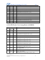
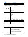
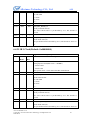
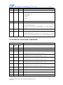
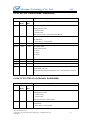
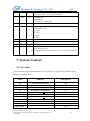
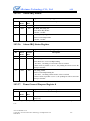
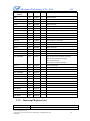
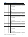
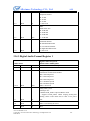
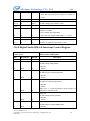
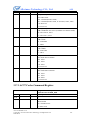
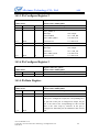
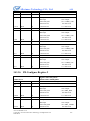
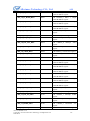
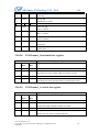
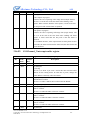
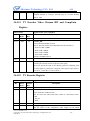
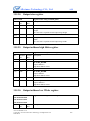
Revision History
Version
Date
Section/ Page
Changes compared to previous issue
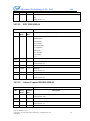
V1.00
2011-8-22
Initial version
V1.01
2011-11-17
Format changes
V1.10
2012-3-29
Audio Codec
Revise some description
V1.20
2012-4-9
USB
Revise some description
A10 User Manual V1.20
Copyright © 2011-2012 Allwinner Technology. All Rights Reserved.
2012-04-09
1
Allwinner Technology CO., Ltd.
A10
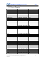
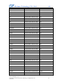
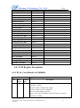
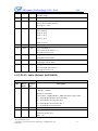
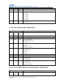
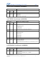
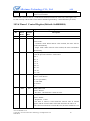
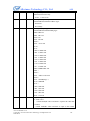
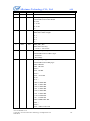
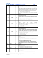
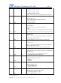
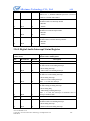
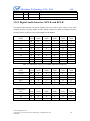
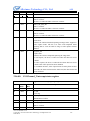
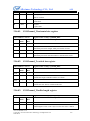
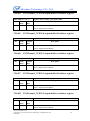
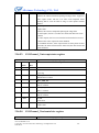
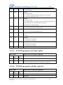
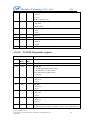
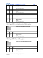
Technical Items
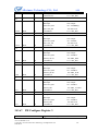
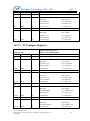
NO.
Abbreviation
Full Name
Description
A processor core designed by ARM Holdings
1
ARM Cortex™-A8
ARM Cortex™-A8
implementing the ARM v7 instruction set
architecture
2
Mali-400
3
SDRAM
Mali-400
Synchronous Dynamic Random
Access Memory
A 2D/3D graphic processor unit designed by
ARM Holdings
Dynamic random access memory (DRAM) that
is synchronized with the system bus
A commonly used technique for controlling
4
PWM
Pulse Width Modulator
power to inertial electrical devices, made
practical by modern electronic power switches
A synchronous serial data link standard named
5
SPI
Serial Peripheral Interface
by Motorola that operates in full duplex mode.
Devices communicate in master/slave mode
where the master device initiates the data frame
6
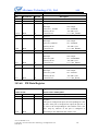
UART
Universal Asynchronous
Receiver/Transmitter
Used
for
serial
communication
with
a
peripheral, modem (data carrier equipment,
DCE) or data set
The allocation of memory storage for use in
7
DMA
Dynamic-Memory-Allocation
a computer program during the run-time of
that program
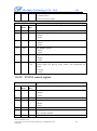
8
I2S
IIS
9
PCM
Pulse Code Modulation
An electrical serial bus interface standard used
for connecting digital audio devices together
Method used to digitally represent sampled
analog signals
Intel Corporation's Audio Codec standard
10
AC97
Audio Codec 97
developed by the Intel Architecture Labs in
1997, and used mainly in motherboards,
modems, and sound cards.
A
11
Audio Codec
Audio Codec
computer
program
implementing
an
algorithm that compresses and decompresses
digital audio data according to a given audio file
format or streaming media audio format.
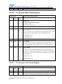
A non-volatile memory card format developed
12
SD
Security Digital3.0
by the SD Card Association for use in portable
devices.
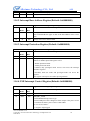
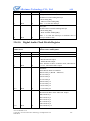
USB On-The-Go
Dual-role controller, which supports both Host
A10 User Manual V1.20
Copyright © 2011-2012 Allwinner Technology. All Rights Reserved.
2012-04-09
2
Allwinner Technology CO., Ltd.
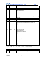
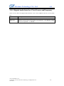
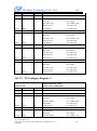
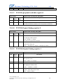
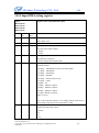
13
USB OTG
A10
and device functions and is full compliant with
the On-The-Go Supplement to the USB 2.0
Specification, Revision 1.0a
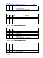
14
EHCI
15
LRADC
16
TP
Enhanced Host Controller
Interface
Low Resolution Analog to
Digital Converter
Touch Panel Controller
A high-speed controller standard that is publicly
specified
A module which can transfer analog signal to
digital signal
A Human-Machine Interactive Interface
A data stream defined by ISO13818-1, which
17
TS
Transport Stream
consists of one or more programs with video
and audio data.
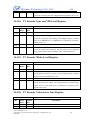
A vehicle bus standard designed to allow
18
CAN
Controller–area network
microcontrollers and devices to communicate
with each other within a vehicle without a host
computer
19
20
PATA
SATA
Parallel Advanced Technology
Attachment
Serial Advanced Technology
Attachment
An old computer bus interface for connecting
hard disk drivers, optical drivers, and compact
flash card
A computer bus interface for connecting host
bus adapters to mass storage devices such as
hard disk drives and optical drives.
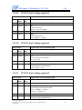
The hardware block that interfaces with
21
CSI
Camera Sensor Interface
different image sensor interfaces and provides a
standard output that can be used for subsequent
image processing.
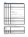
22
HDMI
High-Definition Multimedia
Interface
A
compact
audio/video
interface
transmitting uncompressed digital data
A10 User Manual V1.20
Copyright © 2011-2012 Allwinner Technology. All Rights Reserved.
2012-04-09
3
for
Allwinner Technology CO., Ltd.
A10
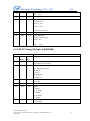
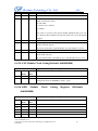
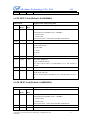
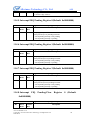
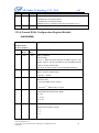
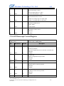
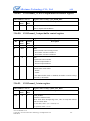
Table of Contents
Revision History ............................................................................................................................................... 1
Technical Items ................................................................................................................................................. 2
1.
Introduction ............................................................................................................................................ 24
1.1. Feature.............................................................................................................................................. 24
1.1.1.
CPU .......................................................................................................................................... 24
1.1.2.
GPU.......................................................................................................................................... 25
1.1.3.
VPU.......................................................................................................................................... 25
1.1.4.
Display Processing Ability ....................................................................................................... 25
1.1.5.
Display Output Ability ............................................................................................................. 25
1.1.6.
Image Input Ability .................................................................................................................. 26
1.1.7.
Memory .................................................................................................................................... 26
1.1.8.
Peripheral ................................................................................................................................. 26
1.1.9.
System ...................................................................................................................................... 27
1.1.10. Security .................................................................................................................................... 27
1.1.11. Package .................................................................................................................................... 27
2.
3.
4.
5.
Pin Description ....................................................................................................................................... 27
2.1.
Pin Placement Table ......................................................................................................................... 27
2.2.
Pin Detail Description ...................................................................................................................... 27
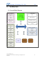
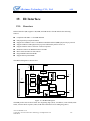
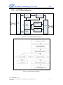
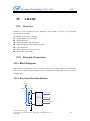
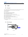
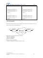
Architecture ............................................................................................................................................ 28
3.1.
General Block Diagram.................................................................................................................... 28
3.2.
Memory Mapping ............................................................................................................................ 29
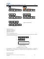
Boot Mode ............................................................................................................................................... 32
4.1.
Overview .......................................................................................................................................... 32
4.2.
Boot Diagram ................................................................................................................................... 33
System Mode........................................................................................................................................... 34
5.1.
6.
Overview .......................................................................................................................................... 34
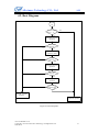
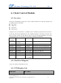
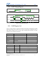
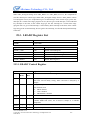
Clock Control Module ........................................................................................................................... 35
6.1.
Overview .......................................................................................................................................... 35
6.2.
Clock Tree Diagram ......................................................................................................................... 35
6.3.
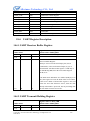
CCM Register List ........................................................................................................................... 35
6.4. CCM Register Description ............................................................................................................... 37
6.4.1.
PLL1-Core(Default: 0x21005000) ........................................................................................... 37
6.4.2.
PLL2-Audio (Default: 0x08100010)........................................................................................ 38
A10 User Manual V1.20
Copyright © 2011-2012 Allwinner Technology. All Rights Reserved.
2012-04-09
4
Allwinner Technology CO., Ltd.
6.4.3.
6.4.4.
6.4.5.
6.4.6.
6.4.7.
6.4.8.
6.4.9.
6.4.10.
6.4.11.
6.4.12.
6.4.13.
6.4.14.
6.4.15.
6.4.16.
6.4.17.
6.4.18.
6.4.19.
6.4.20.
6.4.21.
6.4.22.
6.4.23.
6.4.24.
6.4.25.
6.4.26.
6.4.27.
6.4.28.
6.4.29.
6.4.30.
6.4.31.
6.4.32.
6.4.33.
6.4.34.
6.4.35.
6.4.36.
6.4.37.
6.4.38.
6.4.39.
6.4.40.
6.4.41.
6.4.42.
6.4.43.
6.4.44.
6.4.45.
6.4.46.
A10
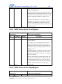
PLL2-Tuning (Default: 0x00000000) ...................................................................................... 39
PLL3-Video 0(Default: 0x0010D063) ..................................................................................... 40
PLL4-VE(Default: 0x21081000) ............................................................................................. 40
PLL5-DDR(Default: 0x11049280) .......................................................................................... 41
PLL6-NC(Default: 0x21009911) ............................................................................................. 42
PLL6-Tuning (Default: ) .......................................................................................................... 43
PLL7-Video 1(Default: 0x0010D063) ..................................................................................... 43
PLL1-Tuning2 (Default: 0x00000000) .................................................................................... 44
PLL5-Tuning2(Default: 0x00000000) ..................................................................................... 44
OSC24M (Default: 0x00138013) ............................................................................................. 45
CPU/AHB/APB0 Clock Ratio(Default: 0x00010010) ............................................................. 45
APB1 Clock Divide Ratio(Default: 0x00000000) ................................................................... 46
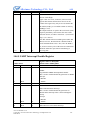
AXI Module Clock Gating(Default: 0x00000000) .................................................................. 47
AHB Module Clock Gating Register 0(Default: 0x00000000) ................................................ 47
AHB Module Clock Gating Register 1(Default: 0x00000000) ................................................ 48
APB0 Module Clock Gating(Default: 0x00000000)................................................................ 49
APB1 Module Clock Gating(Default: 0x00000000)................................................................ 50
NAND Clock(Default: 0x00000000) ....................................................................................... 51
SD/MMC 0 Clock(Default: 0x00000000)................................................................................ 51
SD/MMC 1 Clock(Default: 0x00000000)................................................................................ 52
SD/MMC 2 Clock(Default: 0x00000000)................................................................................ 53
SD/MMC 3 Clock(Default: 0x00000000)................................................................................ 53
TS Clock(Default: 0x00000000) .............................................................................................. 54
SS Clock(Default: 0x00000000) .............................................................................................. 55
SPI0 Clock(Default: 0x00000000) ........................................................................................... 55
SPI1 Clock(Default: 0x00000000) ........................................................................................... 56
SPI2 Clock(Default: 0x00000000) ........................................................................................... 57
IR 0 Clock(Default: 0x00000000)............................................................................................ 57
IR 1 Clock(Default: 0x00000000)............................................................................................ 58
IIS Clock(Default: 0x00000000).............................................................................................. 59
AC97 Clock(Default: 0x00030000) ......................................................................................... 59
Keypad Clock(Default: 0x0000001F) ...................................................................................... 60
NC Clock(Default: 0x00000000) ............................................................................................. 60
USB Clock(Default: 0x00000000) ........................................................................................... 61
SPI3 Clock(Default: 0x00000000) ........................................................................................... 61
DRAM CLK(Default: 0x00000000) ........................................................................................ 62
DE-BE 0 Clock(Default: 0x00000000) .................................................................................... 63
DE-BE 1 Clock(Default: 0x00000000) .................................................................................... 64
DE-FE 0 Clock(Default: 0x00000000) .................................................................................... 64
DE-FE 1 Clock(Default: 0x00000000) .................................................................................... 65
DE-MP Clock(Default: 0x00000000) ...................................................................................... 66
LCD 0 CH0 Clock(Default: 0x00000000) ............................................................................... 66
LCD 1 CH0 Clock(Default: 0x00000000) ............................................................................... 67
CSI-ISP(Default: 0x00000000) ................................................................................................ 67
A10 User Manual V1.20
Copyright © 2011-2012 Allwinner Technology. All Rights Reserved.
2012-04-09
5
Allwinner Technology CO., Ltd.
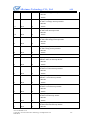
6.4.47.
6.4.48.
6.4.49.
6.4.50.
6.4.51.
6.4.52.
6.4.53.
6.4.54.
6.4.55.
6.4.56.
6.4.57.
6.4.58.
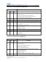
7.
A10
TVD Clock(Default: 0x00000000) .......................................................................................... 68
LCD 0 CH1 Clock(Default: 0x00000000) ............................................................................... 68
LCD 1 CH1 Clock(Default: 0x00000000) ............................................................................... 69
CSI 0 Clock(Default: 0x00000000) ......................................................................................... 70
CSI 1 Clock(Default: 0x00000000) ......................................................................................... 71
VE Clock(Default: 0x00000000) ............................................................................................. 72
Audio Codec Clock(Default: 0x00000000) ............................................................................. 72
AVS Clock(Default: 0x00000000) ........................................................................................... 73
ACE Clock(Default: 0x00000000)........................................................................................... 73
LVDS Clock(Default: 0x00000000) ........................................................................................ 74
HDMI Clock(Default: 0x00000000) ........................................................................................ 74
Mali400 Clock(Default: 0x00000000) ..................................................................................... 74
System Control ....................................................................................................................................... 75
7.1.
Overview .......................................................................................................................................... 75
7.2.
System Control Register List ........................................................................................................... 76
7.3. System Control Register .................................................................................................................. 76
7.3.1.
SRAM Control Register 0(Default: 0x7FFFFFFF) .................................................................. 76
7.3.2.
SRAM Control Register 1(Default: 0x00001300) ................................................................... 76
8.
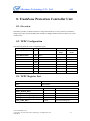
TrustZone Protection Controller Unit .................................................................................................. 78
8.1.
Overview .......................................................................................................................................... 78
8.2.
TZPC Configuration ........................................................................................................................ 78
8.3.
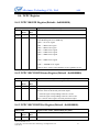
TZPC Register List .......................................................................................................................... 78
8.4. TZPC Register.................................................................................................................................. 79
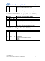
8.4.1.
TZPC R0SIZE Register(Default : 0x00000010) ...................................................................... 79
8.4.2.
TZPC DECPORT0Status Register(Default : 0x00000000)...................................................... 79
8.4.3.
TZPC DECPORT0Set Register(Default : 0x00000000) .......................................................... 79
8.4.4.
TZPC DECPORT0Clear Register(Default : 0x00000000)....................................................... 80
8.4.5.
CPU Control Register(Default :0x00000002) .......................................................................... 80
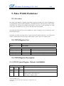
9.
Pulse Width Modulator ......................................................................................................................... 81
9.1.
Overview .......................................................................................................................................... 81
9.2.
PWM Register List........................................................................................................................... 81
9.3. PWM Register Description .............................................................................................................. 81
9.3.1.
PWM Control Register (Default: 0x00000000) ....................................................................... 81
9.3.2.
PWM Channel 0 Period Register ............................................................................................. 83
9.3.3.
PWM Channel 1 Period Register ............................................................................................. 84
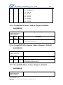
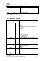
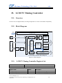
10. Timer Controller .................................................................................................................................... 85
10.1. Overview .......................................................................................................................................... 85
A10 User Manual V1.20
Copyright © 2011-2012 Allwinner Technology. All Rights Reserved.
2012-04-09
6
Allwinner Technology CO., Ltd.
A10
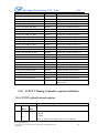
10.2. Timer Register List........................................................................................................................... 85
10.3. Timer Programmable Register ......................................................................................................... 86
10.3.1. Timer IRQ Enable Register(Default: 0x00000000) ................................................................. 86
10.3.2. Timer IRQ Status Register(Default: 0x00000000) ................................................................... 87
10.3.3. Timer 0 Control Register(Default: 0x00000004) ..................................................................... 88
10.3.4. Timer 0 Interval Value Register ............................................................................................... 89
10.3.5. Timer 0 Current Value Register ................................................................................................ 89
10.3.6. Timer 1 Control Register(Default: 0x00000004) ..................................................................... 90
10.3.7. Timer 1 Interval Value Register ............................................................................................... 91
10.3.8. Timer 1 Current Value Register ................................................................................................ 91
10.3.9. Timer 2 Control Register(Default: 0x00000004) ..................................................................... 91
10.3.10. Timer 2 Interval Value Register ............................................................................................... 92
10.3.11. Timer 2 Current Value Register ................................................................................................ 93
10.3.12. Timer 3 Control Register(Default: 0x00000000) ..................................................................... 93
10.3.13. Timer 3 Interval Value .............................................................................................................. 93
10.3.14. Timer 4 Control Register(Default: 0x00000004) ..................................................................... 94
10.3.15. Timer 4 Interval Value Register ............................................................................................... 95
10.3.16. Timer 4 Current Value Register ................................................................................................ 95
10.3.17. Timer 5 Control Register(Default: 0x00000004) ..................................................................... 95
10.3.18. Timer 5 Interval Value Register ............................................................................................... 96
10.3.19. Timer 5 Current Value Register ................................................................................................ 97
10.3.20. AVS Counter Control Register(Default: 0x00000000) ............................................................ 97
10.3.21. AVS Counter 0 Register(Default: 0x00000000)....................................................................... 98
10.3.22. AVS Counter 1 Register(Default: 0x00000000)....................................................................... 98
10.3.23. AVS Counter Divisor Register(Default: 0x05DB05DB).......................................................... 98
10.3.24. Watch Dog Control Register .................................................................................................... 99
10.3.25. Watch-Dog Mode Register(Default: 0x00000000) .................................................................. 99
10.3.26. 64-bit Counter Low Register(Default: 0x00000000) ............................................................. 100
10.3.27. 64-bit Counter High Register(Default: 0x00000000)............................................................. 100
10.3.28. 64-bit Counter Control Register(Default: 0x00000000) ........................................................ 101
10.3.29. LOSC Control(Default: 0x00004000) .................................................................................... 101
10.3.30. RTC YY-MM-DD(Default: 0x00000000) .............................................................................. 102
10.3.31. RTC HH-MM-SS ................................................................................................................... 103
10.3.32. Alarm Counter DD-HH-MM-SS ............................................................................................ 103
10.3.33. Alarm Week HH-MM-SS ....................................................................................................... 104
10.3.34. Alarm Enable ......................................................................................................................... 104
10.3.35. Alarm IRQ Enable.................................................................................................................. 106
10.3.36. Alarm IRQ Status Register ..................................................................................................... 106
10.3.37. Timer General Purpose Register 0 ......................................................................................... 106
10.3.38. Timer General Purpose Register 1 ......................................................................................... 107
10.3.39. Timer General Purpose Register 2 ......................................................................................... 107
10.3.40. Timer General Purpose Register 3 ......................................................................................... 107
10.3.41. CPU Config Register(Default: 0x000000C0) ........................................................................ 107
A10 User Manual V1.20
Copyright © 2011-2012 Allwinner Technology. All Rights Reserved.
2012-04-09
7
Allwinner Technology CO., Ltd.
A10
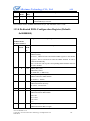
11. Interrupt Controller............................................................................................................................. 109
11.1.
Overview ........................................................................................................................................ 109
11.2.
Interrupt Source.............................................................................................................................. 109
11.3.
Interrupt Register List .................................................................................................................... 111
11.4. Interrupt Programmable Register ................................................................................................... 112
11.4.1. Interrupt Vector Register(Default: 0x00000000).................................................................... 112
11.4.2. Interrupt Base Address Register(Default: 0x00000000) ........................................................ 113
11.4.3. Interrupt Protection Register(Default: 0x00000000).............................................................. 113
11.4.4. NMI Interrupt Control Register(Default: 0x00000000) ......................................................... 113
11.4.5. Interrupt IRQ Pending Register 0(Default: 0x00000000) ...................................................... 114
11.4.6. Interrupt IRQ Pending Register 1(Default: 0x00000000) ...................................................... 114
11.4.7. Interrupt IRQ Pending Register 2(Default: 0x00000000) ...................................................... 114
11.4.8. Interrupt FIQ Pending/Clear Register 0 (Default: 0x00000000) ............................................ 114
11.4.9. Interrupt FIQ Pending/Clear Register 1(Default: 0x00000000) ............................................. 115
11.4.10. Interrupt FIQ Pending/Clear Register 2(Default: 0x00000000) ............................................. 115
11.4.11. Interrupt Select Register 0(Default: 0x00000000) ................................................................. 115
11.4.12. Interrupt Select Register 1(Default: 0x00000000) ................................................................. 116
11.4.13. Interrupt Select Register 2(Default: 0x00000000) ................................................................. 116
11.4.14. Interrupt Enable Register 0(Default: 0x00000000) ................................................................ 116
11.4.15. Interrupt Enable Register 1(Default: 0x00000000) ................................................................ 116
11.4.16. Interrupt Enable Register 2(Default: 0x00000000) ................................................................ 117
11.4.17. Interrupt Mask Register 0(Default: 0x00000000) .................................................................. 117
11.4.18. Interrupt Mask Register 1(Default: 0x00000000) .................................................................. 117
11.4.19. Interrupt Mask Register 2(Default: 0x00000000) .................................................................. 117
11.4.20. Interrupt Response Register 0(Default: 0x00000000)............................................................ 118
11.4.21. Interrupt Response Register 1(Default: 0x00000000)............................................................ 118
11.4.22. Interrupt Response Register 2(Default: 0x00000000)............................................................ 118
11.4.23. Interrupt Fast Forcing Register 0(Default: 0x00000000) ....................................................... 118
11.4.24. Interrupt Fast Forcing Register 1(Default: 0x00000000) ....................................................... 119
11.4.25. Interrupt Fast Forcing Register 2(Default: 0x00000000) ....................................................... 119
11.4.26. Interrupt Source Priority 0 Register(Default: 0x00000000) ................................................... 119
11.4.27. Interrupt Source Priority 1 Register (Default: 0x00000000) .................................................. 122
11.4.28. Interrupt Source Priority 2 Register(Default: 0x00000000) ................................................... 124
11.4.29. Interrupt Source Priority 3 Register(Default: 0x00000000) ................................................... 127
11.4.30. Interrupt Source Priority 4 Register(Default: 0x00000000) ................................................... 130
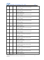
12. DMA Controller ................................................................................................................................... 134
12.1. Overview ........................................................................................................................................ 134
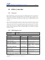
12.2. DMA Register List ......................................................................................................................... 134
12.3. DMA Programmable Register ........................................................................................................ 135
12.3.1. DMA IRQ Enable Register(Default: 0x00000000) ................................................................ 135
12.3.2. DMA IRQ Pending Status Register(Default: 0x00000000) ................................................... 137
A10 User Manual V1.20
Copyright © 2011-2012 Allwinner Technology. All Rights Reserved.
2012-04-09
8
Allwinner Technology CO., Ltd.
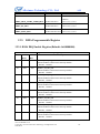
12.3.3.
12.3.4.
12.3.5.
12.3.6.
12.3.7.
12.3.8.
12.3.9.
12.3.10.
12.3.11.
12.3.12.
A10
NDMA Auto Gating Register(Default: 0x00000000) ............................................................ 140
Normal DMA Configuration Register(Default: 0x00000000) ............................................... 141
Normal DMA Source Address Register (Default: 0x00000000) ............................................ 144
Normal DMA Destination Address Register (Default: 0x00000000) .................................... 144
Normal DMA Byte Counter Register (Default: 0x00000000) ............................................... 144
Dedicated DMA Configuration Register (Default: 0x00000000) .......................................... 145
Dedicated DMA Source Start Address Register(N=0:7) ........................................................ 148
Dedicated DMA Destination Start Address Register.............................................................. 148
Dedicated DMA Byte Counter Register ................................................................................. 149
Dedicated DMA Parameter Register ...................................................................................... 149
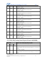
13. SDRAM Controller .............................................................................................................................. 150
13.1. Overview ........................................................................................................................................ 150
14. NAND Flash Controller ....................................................................................................................... 151
14.1. Overview ........................................................................................................................................ 151
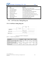
15. SD3.0 Controller................................................................................................................................... 152
15.1. Overview ........................................................................................................................................ 152
15.2. SD3.0 Timing Diagram .................................................................................................................. 152
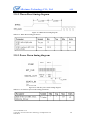
16. Two Wire Interface .............................................................................................................................. 153
16.1. Overview ........................................................................................................................................ 153
16.2. TWI Controller Timing Diagram ................................................................................................... 153
16.3. TWI Controller Register List ......................................................................................................... 154
16.4. TWI Controller Register Description ............................................................................................. 154
16.4.1. TWI Slave Address Register .................................................................................................. 154
16.4.2. TWI Extend Address Register ................................................................................................ 155
16.4.3. TWI Data Register ................................................................................................................. 155
16.4.4. TWI Control Register ............................................................................................................. 155
16.4.5. TWI Status Register ............................................................................................................... 158
16.4.6. TWI Clock Register ............................................................................................................... 159
16.4.7. TWI Soft Reset Register ........................................................................................................ 159
16.4.8. TWI Enhance Feature Register .............................................................................................. 160
16.4.9. TWI Line Control Register .................................................................................................... 160
16.4.10. TWI DVFS Control Register ................................................................................................. 161
16.5. TWI Controller Special Requirement ............................................................................................ 161
16.5.1. TWI Pin List........................................................................................................................... 161
16.5.2. TWI Controller Operation ...................................................................................................... 162
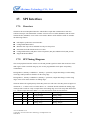
17. SPI Interface ......................................................................................................................................... 163
17.1. Overview ........................................................................................................................................ 163
A10 User Manual V1.20
Copyright © 2011-2012 Allwinner Technology. All Rights Reserved.
2012-04-09
9
Allwinner Technology CO., Ltd.
A10
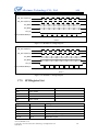
17.2. SPI Timing Diagram ...................................................................................................................... 163
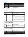
17.3. SPI Register List ............................................................................................................................ 164
17.4. SPI Register Description ................................................................................................................ 165
17.4.1. SPI RX Data Register............................................................................................................. 165
17.4.2. SPI TX Data Register ............................................................................................................. 165
17.4.3. SPI Control Register .............................................................................................................. 165
17.4.4. SPI Interrupt Control Register................................................................................................ 168
17.4.5. SPI Interrupt Status Register .................................................................................................. 170
17.4.6. SPI DMA Control Register .................................................................................................... 172
17.4.7. SPI Wait Clock Register ......................................................................................................... 174
17.4.8. SPI Clock Control Register .................................................................................................... 174
17.4.9. SPI Burst Counter Register .................................................................................................... 175
17.4.10. SPI Transmit Counter Register............................................................................................... 175
17.4.11. SPI FIFO Status Register ....................................................................................................... 175
17.4.12. SPI Special Requirement........................................................................................................ 176
17.4.13. SPI Pin List ............................................................................................................................ 176
17.4.14. SPI Module Clock Source and Frequency ............................................................................. 176
18. UART Interface .................................................................................................................................... 178
18.1. Overview ........................................................................................................................................ 178
18.2. UART Timing Diagram.................................................................................................................. 179
18.3. UART Register List........................................................................................................................ 179
18.4. UART Register Description ........................................................................................................... 180
18.4.1. UART Receiver Buffer Register ............................................................................................ 180
18.4.2. UART Transmit Holding Register .......................................................................................... 180
18.4.3. UART Divisor Latch Low Register........................................................................................ 181
18.4.4. UART Divisor Latch High Register ....................................................................................... 181
18.4.5. UART Interrupt Enable Register ............................................................................................ 182
18.4.6. UART Interrupt Identity Register........................................................................................... 183
18.4.7. UART FIFO Control Register ................................................................................................ 185
18.4.8. UART Line Control Register ................................................................................................. 186
18.4.9. UART Modem Control Register ............................................................................................ 188
18.4.10. UART Line Status Register .................................................................................................... 189
18.4.11. UART Modem Status Register ............................................................................................... 192
18.4.12. UART Scratch Register .......................................................................................................... 194
18.4.13. UART Status Register ............................................................................................................ 195
18.4.14. UART Transmit FIFO Level Register .................................................................................... 196
18.4.15. UART Receive FIFO Level Register ..................................................................................... 196
18.4.16. UART Halt TX Register ......................................................................................................... 196
18.5. UART Special Requirement ........................................................................................................... 197
18.5.1. UART Pin List........................................................................................................................ 197
A10 User Manual V1.20
Copyright © 2011-2012 Allwinner Technology. All Rights Reserved.
2012-04-09
10
Allwinner Technology CO., Ltd.
A10
19. IR Interface........................................................................................................................................... 199
19.1. Overview ........................................................................................................................................ 199
19.2. IR Timing Diagram ........................................................................................................................ 201
19.3. IR Register List .............................................................................................................................. 201
19.4. IR Register Description .................................................................................................................. 202
19.4.1. IR Control Register ................................................................................................................ 202
19.4.2. IR Transmitter Configure Register ......................................................................................... 203
19.4.3. IR Transmitter Address Register ............................................................................................ 204
19.4.4. IR Transmitter Counter Register ............................................................................................ 204
19.4.5. IR Receiver Configure Register ............................................................................................. 205
19.4.6. IR Receiver Address Register ................................................................................................ 205
19.4.7. IR Receiver Counter Register ................................................................................................ 206
19.4.8. IR Transmitter FIFO Register ................................................................................................ 206
19.4.9. IR Receiver FIFO Register..................................................................................................... 206
19.4.10. IR Transmitter Interrupt Control Register .............................................................................. 207
19.4.11. IR Transmitter Status Register ............................................................................................... 208
19.4.12. IR Receiver Interrupt Control Register .................................................................................. 209
19.4.13. IR Receiver Status Register.................................................................................................... 210
19.4.14. CIR Configure Register.......................................................................................................... 211
20. USB_OTG Controller .......................................................................................................................... 215
20.1. Overview ........................................................................................................................................ 215
20.2. USB_OTG Timing Diagram .......................................................................................................... 215
21. USB Host Controller ............................................................................................................................ 216
21.1. Overview ........................................................................................................................................ 216
21.2. USB Host Timing Diagram ............................................................................................................ 217
22. Digital Audio Interface ........................................................................................................................ 218
22.1. Overview ........................................................................................................................................ 218
22.2. Digital Audio Interface Timing Diagram ....................................................................................... 219
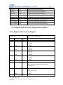
22.3. Digital Audio Interface Register List ............................................................................................. 220
22.4. Digital Audio Interface Register Description ................................................................................. 221
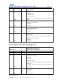
22.4.1. Digital Audio Control Register .............................................................................................. 221
22.4.2. Digital Audio Format Register 0 ............................................................................................ 222
22.4.3. Digital Audio Format Register 1 ............................................................................................ 223
22.4.4. Digital Audio TX FIFO Register ............................................................................................ 225
22.4.5. Digital Audio RX FIFO register ............................................................................................. 225
22.4.6. Digital Audio FIFO Control Register ..................................................................................... 225
22.4.7. Digital Audio FIFO Status Register ....................................................................................... 226
22.4.8. Digital Audio DMA & Interrupt Control Register ................................................................. 227
A10 User Manual V1.20
Copyright © 2011-2012 Allwinner Technology. All Rights Reserved.
2012-04-09
11
Allwinner Technology CO., Ltd.
22.4.9.
22.4.10.
22.4.11.
22.4.12.
22.4.13.
22.4.14.
22.4.15.
22.4.16.
A10
Digital Audio Interrupt Status Register .................................................................................. 228
Digital Audio Clock Divide Register ..................................................................................... 229
Digital Audio TX Counter register ......................................................................................... 230
Digital Audio RX Counter register......................................................................................... 230
Digital Audio TX Channel Select register .............................................................................. 230
Digital Audio TX Channel Mapping Register ........................................................................ 231
Digital Audio RX Channel Select register ............................................................................. 233
Digital Audio RX Channel Mapping Register ....................................................................... 233
22.5. Digital Audio Interface Special Requirement ................................................................................ 234
22.5.1. Digital Audio Interface Pin List ............................................................................................. 234
22.5.2. Digital Audio Interface MCLK and BCLK ............................................................................ 235
22.5.3. Digital Audio Interface Clock Source andFrequency............................................................. 236
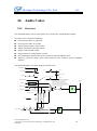
23. AC97 Interface ..................................................................................................................................... 237
23.1. Overview ........................................................................................................................................ 237
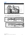
23.2. AC97 Block diagram ..................................................................................................................... 238
23.3. AC97 Interface clock tree .............................................................................................................. 239
23.4. AC Link frame Format ................................................................................................................... 239
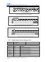
23.5. AC97 Interface Timing Diagram ................................................................................................... 240
23.5.1. Cold Reset timing diagram..................................................................................................... 240
23.5.2. Warm Reset timing diagram ................................................................................................... 241
23.5.3. Power Down timing diagram ................................................................................................. 241
23.5.4. AC-link Clock ........................................................................................................................ 242
23.5.5. Data transmission timing diagram.......................................................................................... 243
23.6. AC97 Interface Register List ......................................................................................................... 245
23.7. AC97 Interface Register Description ............................................................................................. 245
23.7.1. AC97 Control Register ........................................................................................................... 245
23.7.2. AC97 Format Register ........................................................................................................... 246
23.7.3. AC97 Codec Command Register ........................................................................................... 247
23.7.4. AC97 Codec Status Register .................................................................................................. 248
23.7.5. AC97 TX FIFO Register ........................................................................................................ 248
23.7.6. AC97 RX FIFO Register ........................................................................................................ 248
23.7.7. AC97 FIFO Control Register ................................................................................................. 248
23.7.8. AC97 FIFO Status Register.................................................................................................... 250
23.7.9. AC97 Interrupt Control Register ............................................................................................ 250
23.7.10. AC97 Interrupt status Register ............................................................................................... 251
23.7.11. AC97 TX Counter register ..................................................................................................... 252
23.7.12. AC97 RX Counter register ..................................................................................................... 253
23.7.13. AC97 Interface Pin list ........................................................................................................... 253
23.8. AC97 Clock Requirement .............................................................................................................. 253
A10 User Manual V1.20
Copyright © 2011-2012 Allwinner Technology. All Rights Reserved.
2012-04-09
12
Allwinner Technology CO., Ltd.
A10
24. Audio Codec ......................................................................................................................................... 254
24.1. Overview ........................................................................................................................................ 254
24.2. Audio Codec Register List ............................................................................................................. 255
24.2.1. DAC Digital Part Control Register ........................................................................................ 255
24.2.2. DAC FIFO Control Register .................................................................................................. 255
24.2.3. DAC FIFO Status Register ..................................................................................................... 257
24.2.4. DAC TX DATA register ......................................................................................................... 258
24.2.5. DAC Analog Control Register ............................................................................................... 258
24.2.6. ADC FIFO Status Register ..................................................................................................... 260
24.2.7. ADC RX DATA register ......................................................................................................... 261
24.2.8. ADC Analog Control Register ............................................................................................... 261
24.2.9. DAC TX Counter register ...................................................................................................... 264
24.2.10. ADC RX Counter register ...................................................................................................... 264
25. LRADC ................................................................................................................................................. 265
25.1. Overview ........................................................................................................................................ 265
25.2. Principle of operation ..................................................................................................................... 265
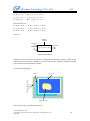
25.2.1. Block Diagram ....................................................................................................................... 265
25.2.2. Key Function Introduction ..................................................................................................... 265
25.3. LRADC Register List ..................................................................................................................... 266
25.3.1. LRADC Control Register ....................................................................................................... 266
25.3.2. LRADC Interrupt Control Register ........................................................................................ 267
25.3.3. LRADC Interrupt Status Register .......................................................................................... 268
25.3.4. LRADC Data 0 Register ........................................................................................................ 270
25.3.5. LRADC Data 1 Register ........................................................................................................ 271
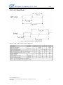
26. TP Controller ........................................................................................................................................ 272
26.1. Overview ........................................................................................................................................ 272
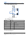
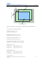
26.2. Typical Application Circuit ............................................................................................................ 273
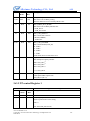
26.3. TP Register List.............................................................................................................................. 273
26.3.1. TP Control Register 0 ............................................................................................................. 273
26.3.2. TP control Register 1.............................................................................................................. 274
26.3.3. TP control Register 2.............................................................................................................. 275
26.4. Median filter Control Register ....................................................................................................... 276
26.4.1. TP Interrupt& FIFO Control Register .................................................................................... 276
26.4.2. TP Interrupt& FIFO Status Register....................................................................................... 277
26.4.3. Common Data Register .......................................................................................................... 278
27. Keypad Interface .................................................................................................................................. 280
27.1. Overview ........................................................................................................................................ 280
27.2. Keypad Interface Register List....................................................................................................... 280
A10 User Manual V1.20
Copyright © 2011-2012 Allwinner Technology. All Rights Reserved.
2012-04-09
13
Allwinner Technology CO., Ltd.
A10
27.3. Keypad Interface Register Description .......................................................................................... 280
27.3.1. Keypad Control Register ........................................................................................................ 280
27.3.2. Keypad Timing Register ........................................................................................................ 281
27.3.3. Keypad Interrupt Configure Register ..................................................................................... 281
27.3.4. Keypad Interrupt Status Register ........................................................................................... 282
27.3.5. Keypad Input Data Register 0 ................................................................................................ 282
27.3.6. Keypad Input Data Register 1 ................................................................................................ 282
27.4. Keypad Interface Pin List............................................................................................................... 282
28. Security System .................................................................................................................................... 284
28.1. Overview ........................................................................................................................................ 284
29. Security ID ............................................................................................................................................ 285
29.1. Overview ........................................................................................................................................ 285
29.2. Security ID Register List ................................................................................................................ 285
29.3. SID Register Description ............................................................................................................... 285
29.3.1. SID Root Key 0 Register........................................................................................................ 285
29.3.2. SID Root Key 1 Register........................................................................................................ 285
29.3.3. SID Root Key 2 Register........................................................................................................ 286
29.3.4. SID Root Key 3 Register........................................................................................................ 286
30. Port Controller ..................................................................................................................................... 287
30.1. Overview ........................................................................................................................................ 287
30.2. Port Register List ........................................................................................................................... 287
30.3. Port Register Description ............................................................................................................... 288
30.3.1. PA Configure Register 0 ......................................................................................................... 288
30.3.2. PA Configure Register 1 ......................................................................................................... 289
30.3.3. PA Configure Register 2 ......................................................................................................... 291
30.3.4. PA Configure Register 3 ......................................................................................................... 291
30.3.5. PA Data Register .................................................................................................................... 291
30.3.6. PA Multi-Driving Register 0 .................................................................................................. 292
30.3.7. PA Multi-Driving Register 1 .................................................................................................. 292
30.3.8. PA Pull Register 0 .................................................................................................................. 292
30.3.9. PA Pull Register 1 .................................................................................................................. 292
30.3.10. PB Configure Register 0 ........................................................................................................ 293
30.3.11. PB Configure Register 1 ........................................................................................................ 294
30.3.12. PB Configure Register 2 ........................................................................................................ 295
30.3.13. PB Configure Register 3 ........................................................................................................ 296
30.3.14. PB Data Register .................................................................................................................... 297
30.3.15. PB Multi-Driving Register 0 .................................................................................................. 297
30.3.16. PB Multi-Driving Register 1 .................................................................................................. 297
30.3.17. PB Pull Register 0 .................................................................................................................. 298
A10 User Manual V1.20
Copyright © 2011-2012 Allwinner Technology. All Rights Reserved.
2012-04-09
14
Allwinner Technology CO., Ltd.
30.3.18.
30.3.19.
30.3.20.
30.3.21.
30.3.22.
30.3.23.
30.3.24.
30.3.25.
30.3.26.
30.3.27.
30.3.28.
30.3.29.
30.3.30.
30.3.31.
30.3.32.
30.3.33.
30.3.34.
30.3.35.
30.3.36.
30.3.37.
30.3.38.
30.3.39.
30.3.40.
30.3.41.
30.3.42.
30.3.43.
30.3.44.
30.3.45.
30.3.46.
30.3.47.
30.3.48.
30.3.49.
30.3.50.
30.3.51.
30.3.52.
30.3.53.
30.3.54.
30.3.55.
30.3.56.
30.3.57.
30.3.58.
30.3.59.
30.3.60.
30.3.61.
A10
PB Pull Register 1 .................................................................................................................. 298
PC Configure Register 0 ........................................................................................................ 298
PC Configure Register 1 ........................................................................................................ 299
PC Configure Register 2 ........................................................................................................ 301
PC Configure Register 3 ........................................................................................................ 302
PC Data Register .................................................................................................................... 302
PC Multi-Driving Register 0 .................................................................................................. 303
PC Multi-Driving Register 1 .................................................................................................. 303
PC Pull Register 0 .................................................................................................................. 303
PC Pull Register 1 .................................................................................................................. 303
PD Configure Register 0 ........................................................................................................ 304
PD Configure Register 1 ........................................................................................................ 305
PD Configure Register 2 ........................................................................................................ 306
PD Configure Register 3 ........................................................................................................ 307
PD Data Register .................................................................................................................... 308
PD Multi-Driving Register 0 .................................................................................................. 309
PD Multi-Driving Register 1 .................................................................................................. 309
PD Pull Register 0 .................................................................................................................. 309
PD Pull Register 1 .................................................................................................................. 309
PE Configure Register 0......................................................................................................... 310
PE Configure Register 1......................................................................................................... 311
PE Configure Register 2......................................................................................................... 312
PE Configure Register 3......................................................................................................... 312
PE Data Register .................................................................................................................... 312
PE Multi-Driving Register 0 .................................................................................................. 312
PE Multi-Driving Register 1 .................................................................................................. 313
PE Pull Register 0 .................................................................................................................. 313
PE Pull Register 1 .................................................................................................................. 313
PF Configure Register 0 ......................................................................................................... 313
PF Configure Register 1 ......................................................................................................... 314
PF Configure Register 2 ......................................................................................................... 314
PF Configure Register 3 ......................................................................................................... 315
PF Data Register .................................................................................................................... 315
PF Multi-Driving Register 0 .................................................................................................. 315
PF Multi-Driving Register 1 .................................................................................................. 315
PF Pull Register 0................................................................................................................... 316
PF Pull Register 1................................................................................................................... 316
PG Configure Register 0 ........................................................................................................ 316
PG Configure Register 1 ........................................................................................................ 317
PG Configure Register 2 ........................................................................................................ 318
PG Configure Register 3 ........................................................................................................ 318
PG Data Register .................................................................................................................... 318
PG Multi-Driving Register 0 .................................................................................................. 319
PG Multi-Driving Register 1 .................................................................................................. 319
A10 User Manual V1.20
Copyright © 2011-2012 Allwinner Technology. All Rights Reserved.
2012-04-09
15
Allwinner Technology CO., Ltd.
30.3.62.
30.3.63.
30.3.64.
30.3.65.
30.3.66.
30.3.67.
30.3.68.
30.3.69.
30.3.70.
30.3.71.
30.3.72.
30.3.73.
30.3.74.
30.3.75.
30.3.76.
30.3.77.
30.3.78.
30.3.79.
30.3.80.
30.3.81.
30.3.82.
30.3.83.
30.3.84.
30.3.85.
30.3.86.
30.3.87.
30.3.88.
A10
PG Pull Register 0 .................................................................................................................. 319
PG Pull Register 1 .................................................................................................................. 319
PH Configure Register 0 ........................................................................................................ 320
PH Configure Register 1 ........................................................................................................ 321
PH Configure Register 2 ........................................................................................................ 322
PH Configure Register 3 ........................................................................................................ 323
PH Data Register .................................................................................................................... 324
PH Multi-Driving Register 0 .................................................................................................. 325
PH Multi-Driving Register 1 .................................................................................................. 325
PH Pull Register 0 .................................................................................................................. 325
PH Pull Register 1 .................................................................................................................. 325
PI Configure Register 0 .......................................................................................................... 326
PI Configure Register 1 .......................................................................................................... 327
PI Configure Register 2 .......................................................................................................... 328
PI Configure Register 3 .......................................................................................................... 329
PI Data Register ..................................................................................................................... 329
PI Multi-Driving Register 0 ................................................................................................... 330
PI Multi-Driving Register 1 ................................................................................................... 330
PI Pull Register 0 ................................................................................................................... 330
PI Pull Register 1 ................................................................................................................... 330
PIO Interrupt Configure Register 0 ........................................................................................ 331
PIO Interrupt Configure Register 1 ........................................................................................ 331
PIO Interrupt Configure Register 2 ........................................................................................ 331
PIO Interrupt Configure Register 3 ........................................................................................ 332
PIO Interrupt Control Register ............................................................................................... 332
PIO Interrupt Status Register ................................................................................................. 332
PIO Interrupt Debounce Register ........................................................................................... 333
31. CSI0 with ISP FE ................................................................................................................................. 334
31.1. Overview ........................................................................................................................................ 334
31.2. Feature............................................................................................................................................ 334
31.2.1. CSI ......................................................................................................................................... 334
31.2.2. ISP FE .................................................................................................................................... 334
31.3. Block diagram ................................................................................................................................ 335
31.3.1. CSI data ports ......................................................................................................................... 335
31.4. Timing ............................................................................................................................................ 335
31.4.1. CSI timing .............................................................................................................................. 335
31.4.2. 16bit YUV422 Timing ........................................................................................................... 336
31.4.3. CCIR656 2 channel Timing ................................................................................................... 336
31.4.4. CCIR656 4 channel Timing ................................................................................................... 337
31.4.5. CCIR656 Header Code .......................................................................................................... 337
31.5. CSI0 Register List .......................................................................................................................... 338
A10 User Manual V1.20
Copyright © 2011-2012 Allwinner Technology. All Rights Reserved.
2012-04-09
16
Allwinner Technology CO., Ltd.
A10
31.6. CSI0 Register Description.............................................................................................................. 343
31.6.1. CSI Enable Register ............................................................................................................... 343
31.6.2. CSI configuration register ...................................................................................................... 343
31.6.3. CSI capture control register ................................................................................................... 345
31.6.4. CSI horizontal scale register .................................................................................................. 346
31.6.5. CSI Channel_0 FIFO 0 output buffer-A address register ....................................................... 346
31.6.6. CSI Channel_0 FIFO 0 output buffer-B address register ....................................................... 346
31.6.7. CSI Channel_0 FIFO 1 output buffer-A address register ....................................................... 347
31.6.8. CSI Channel_0 FIFO 1 output buffer-B address register ....................................................... 347
31.6.9. CSI Channel_0 FIFO 2 output buffer-A address register ....................................................... 347
31.6.10. CSI Channel_0 FIFO 2 output buffer-B address register ....................................................... 347
31.6.11. CSI Channel_0 output buffer control register ........................................................................ 347
31.6.12. CSI Channel_0 status register ................................................................................................ 348
31.6.13. CSI Channel_0 interrupt enable register ................................................................................ 349
31.6.14. CSI Channel_0 interrupt status register ................................................................................. 350
31.6.15. CSI Channel_0 horizontal size register .................................................................................. 350
31.6.16. CSI Channel_0 vertical size register ...................................................................................... 350
31.6.17. CSI Channel_0 buffer length register ..................................................................................... 351
31.6.18. CSI Channel_1 FIFO 0 output buffer-A address register ....................................................... 351
31.6.19. CSI Channel_1 FIFO 0 output buffer-B address register ....................................................... 351
31.6.20. CSI Channel_1 FIFO 1 output buffer-A address register ....................................................... 351
31.6.21. CSI Channel_1 FIFO 1 output buffer-B address register ....................................................... 352
31.6.22. CSI Channel_1 FIFO 2 output buffer-A address register ....................................................... 352
31.6.23. CSI Channel_1 FIFO 2 output buffer-B address register ....................................................... 352
31.6.24. CSI Channel_1 output buffer control register ........................................................................ 352
31.6.25. CSI Channel_1 status register ................................................................................................ 353
31.6.26. CSI Channel_1 interrupt enable register ................................................................................ 353
31.6.27. CSI Channel_1 interrupt status register ................................................................................. 354
31.6.28. CSI Channel_1 horizontal size register .................................................................................. 355
31.6.29. CSI Channel_1 vertical size register ...................................................................................... 355
31.6.30. CSI Channel_1 buffer length register ..................................................................................... 356
31.6.31. CSI Channel_2 FIFO 0 output buffer-A address register ....................................................... 356
31.6.32. CSI Channel_2 FIFO 0 output buffer-B address register ....................................................... 356
31.6.33. CSI Channel_2 FIFO 1 output buffer-A address register ....................................................... 356
31.6.34. CSI Channel_2 FIFO 1 output buffer-B address register ....................................................... 356
31.6.35. CSI Channel_2 FIFO 2 output buffer-A address register ....................................................... 357
31.6.36. CSI Channel_2 FIFO 2 output buffer-B address register ....................................................... 357
31.6.37. CSI Channel_2 output buffer control register ........................................................................ 357
31.6.38. CSI Channel_2 status register ................................................................................................ 358
31.6.39. CSI Channel_2 interrupt enable register ................................................................................ 358
31.6.40. CSI Channel_2 interrupt status register ................................................................................. 359
31.6.41. CSI Channel_2 horizontal size register .................................................................................. 360
31.6.42. CSI Channel_2 vertical size register ...................................................................................... 360
31.6.43. CSI Channel_2 buffer length register ..................................................................................... 360
A10 User Manual V1.20
Copyright © 2011-2012 Allwinner Technology. All Rights Reserved.
2012-04-09
17
Allwinner Technology CO., Ltd.
31.6.44.
31.6.45.
31.6.46.
31.6.47.
31.6.48.
31.6.49.
31.6.50.
31.6.51.
31.6.52.
31.6.53.
31.6.54.
31.6.55.
31.6.56.
31.6.57.
31.6.58.
31.6.59.
31.6.60.
31.6.61.
31.6.62.
31.6.63.
31.6.64.
31.6.65.
31.6.66.
31.6.67.
31.6.68.
31.6.69.
31.6.70.
31.6.71.
31.6.72.
31.6.73.
31.6.74.
31.6.75.
31.6.76.
31.6.77.
31.6.78.
31.6.79.
31.6.80.
31.6.81.
31.6.82.
31.6.83.
31.6.84.
31.6.85.
31.6.86.
31.6.87.
A10
CSI Channel_3 FIFO 0 output buffer-A address register ....................................................... 361
CSI Channel_3 FIFO 0 output buffer-B address register ....................................................... 361
CSI Channel_3 FIFO 1 output buffer-A address register ....................................................... 361
CSI Channel_3 FIFO 1 output buffer-B address register ....................................................... 361
CSI Channel_3 FIFO 2 output buffer-A address register ....................................................... 361
CSI Channel_3 FIFO 2 output buffer-B address register ....................................................... 362
CSI Channel_3 output buffer control register ........................................................................ 362
CSI Channel_3 status register ................................................................................................ 362
CSI Channel_3 interrupt enable register ................................................................................ 363
CSI Channel_3 interrupt status register ................................................................................. 364
CSI Channel_3 horizontal size register .................................................................................. 364
CSI Channel_3 vertical size register ...................................................................................... 365
CSI Channel_3 buffer length register ..................................................................................... 365
ISP Enable register ................................................................................................................. 365
ISP Mode register ................................................................................................................... 366
ISP OBC Image Black size register........................................................................................ 367
ISP OBC Image Valid size register ........................................................................................ 367
ISP OBC Image Start register................................................................................................. 367
ISP OBC configuration register ............................................................................................. 368
ISP Horizontal OBC window start register ............................................................................ 368
ISP Vertical OBC window start register ................................................................................. 369
ISP Vertical OBC parameter register ...................................................................................... 369
ISP OBC fixed value register ................................................................................................. 369
ISP OBC offset register .......................................................................................................... 370
ISP OBC clamp value register................................................................................................ 370
ISP LSC configuration register .............................................................................................. 370
ISP LSC gain factor address register ...................................................................................... 371
ISP LSC gain factor address length register ........................................................................... 371
ISP Offset register .................................................................................................................. 371
ISP Gain Factor register ......................................................................................................... 371
ISP Dark Frame Enable register ............................................................................................. 372
ISP Dark Frame buffer address register ................................................................................. 372
ISP Dark Frame buffer address length register ...................................................................... 372
ISP luma DC subtraction value register ................................................................................. 373
ISP H3A Median filter threshold register ............................................................................... 373
ISP AF window number register ............................................................................................ 373
ISP AF window size register .................................................................................................. 374
ISP AF window start register.................................................................................................. 374
ISP AF configuration register ................................................................................................. 374
ISP AF filter parameter 0 register........................................................................................... 375
ISP AF filter parameter 1 register........................................................................................... 375
ISP AF filter parameter 2 register........................................................................................... 375
ISP AWBE window number register ...................................................................................... 376
ISP AWBE window size register ............................................................................................ 376
A10 User Manual V1.20
Copyright © 2011-2012 Allwinner Technology. All Rights Reserved.
2012-04-09
18
Allwinner Technology CO., Ltd.
A10
31.6.88. ISP AWBE window start register ........................................................................................... 376
31.6.89. ISP AWBE configuration register .......................................................................................... 377
31.6.90. ISP Histogram region 0 window size register ........................................................................ 377
31.6.91. ISP Histogram region 0 window start register ....................................................................... 377
31.6.92. ISP Histogram region 1 window size register ........................................................................ 378
31.6.93. ISP Histogram region 1 window start register ....................................................................... 378
31.6.94. ISP Histogram region 2 window size register ........................................................................ 378
31.6.95. ISP Histogram region 2 window start register ....................................................................... 379
31.6.96. ISP Histogram region 3 window size register ........................................................................ 379
31.6.97. ISP Histogram region 3 window start register ....................................................................... 379
31.6.98. ISP 3A Statistics output address register ................................................................................ 380
31.6.99. ISP LUT Defect Correction configuration register ................................................................ 380
31.6.100. ISP LUT Defect Correction address register .......................................................................... 380
31.6.101. ISP FE Y/Raw Output address length register ....................................................................... 381
31.6.102. SP FE Y/Raw Output address register .................................................................................... 381
31.6.103. ISP interrupt enable register ................................................................................................... 381
31.6.104. ISP interrupt status register .................................................................................................... 382
31.6.105. ISP FE CbCr Output address length register .......................................................................... 382
31.6.106. ISP FE CbCr Output address register ..................................................................................... 383
32. CSI1 ....................................................................................................................................................... 384
32.1. Overview ........................................................................................................................................ 384
32.2. Block diagram ................................................................................................................................ 384
32.3. CSI data ports ................................................................................................................................. 385
32.4. Timing ............................................................................................................................................ 385
32.4.1. CSI timing .............................................................................................................................. 385
32.5. CSI1 Registers List ........................................................................................................................ 385
32.6. CSI1 Register Description.............................................................................................................. 386
32.6.1. CSI Enable Register ............................................................................................................... 386
32.6.2. CSI configuration register ...................................................................................................... 387
32.6.3. CSI capture control register ................................................................................................... 389
32.6.4. CSI horizontal scale register .................................................................................................. 389
32.6.5. CSI Channel_0 FIFO 0 output buffer-A address register ....................................................... 390
32.6.6. CSI Channel_0 FIFO 0 output buffer-B address register ....................................................... 390
32.6.7. CSI Channel_0 FIFO 1 output buffer-A address register ....................................................... 390
32.6.8. CSI Channel_0 FIFO 1 output buffer-B address register ....................................................... 391
32.6.9. CSI Channel_0 FIFO 2 output buffer-A address register ....................................................... 391
32.6.10. CSI Channel_0 FIFO 2 output buffer-B address register ....................................................... 391
32.6.11. CSI Channel_0 output buffer control register ........................................................................ 391
32.6.12. CSI Channel_0 status register ................................................................................................ 392
32.6.13. CSI Channel_0 interrupt enable register ................................................................................ 393
32.6.14. CSI Channel_0 interrupt status register ................................................................................. 394
A10 User Manual V1.20
Copyright © 2011-2012 Allwinner Technology. All Rights Reserved.
2012-04-09
19
Allwinner Technology CO., Ltd.
A10
32.6.15. CSI Channel_0 horizontal size register .................................................................................. 394
32.6.16. CSI Channel_0 vertical size register ...................................................................................... 394
32.6.17. CSI Channel_0 buffer length register ..................................................................................... 395
33. LCD/TV Timing Controller ................................................................................................................ 396
33.1. Overview ........................................................................................................................................ 396
33.2. Block Diagram ............................................................................................................................... 396
33.3. LCD/TV Timing Controller Register List ...................................................................................... 396
33.4. LCD/TV Timing Controller registers definition ............................................................................ 398
33.4.1. TCON global control register................................................................................................. 398
33.4.2. TCON global interrupt register0 ............................................................................................ 399
33.4.3. TCON global interrupt register1 ............................................................................................ 400
33.4.4. TCON FRM control register .................................................................................................. 400
33.4.5. TCON FRM seed register ...................................................................................................... 401
33.4.6. TCON FRM table register ...................................................................................................... 402
33.4.7. TCON0 control register.......................................................................................................... 402
33.4.8. TCON0 data clock register..................................................................................................... 403
33.4.9. TCON0 basic timing register0 ............................................................................................... 404
33.4.10. TCON0 basic timing register1 ............................................................................................... 404
33.4.11. TCON0 basic timing register2 ............................................................................................... 405
33.4.12. TCON0 basic timing register3 ............................................................................................... 405
33.4.13. TCON0 hv panel interface register ........................................................................................ 405
33.4.14. TCON0 cpu panel interface register....................................................................................... 406
33.4.15. TCON0 cpu panel write data register ..................................................................................... 407
33.4.16. TCON0 cpu panel read data register0 .................................................................................... 407
33.4.17. TCON0 cpu panel read data register1 .................................................................................... 408
33.4.18. TCON0 ttl panel timing register 0.......................................................................................... 408
33.4.19. TCON0 tttl panel timing register 1 ........................................................................................ 408
33.4.20. TCON0 ttl panel timing register 2.......................................................................................... 409
33.4.21. TCON0 ttl panel timing register3........................................................................................... 409
33.4.22. TCON0 ttl panel timing register3........................................................................................... 409
33.4.23. TCON0 lvds panel interface register ...................................................................................... 410
33.4.24. TCON0 IO polarity register ................................................................................................... 411
33.4.25. TCON1 control register.......................................................................................................... 412
33.4.26. TCON1 basic timing register0 ............................................................................................... 413
33.4.27. TCON1 basic timing register1 ............................................................................................... 413
33.4.28. TCON1 basic timing register2 ............................................................................................... 413
33.4.29. TCON1 basic timing register3 ............................................................................................... 414
33.4.30. TCON1 basic timing register4 ............................................................................................... 414
33.4.31. TCON1 basic timing register5 ............................................................................................... 414
33.4.32. TCON1 IO polarity register ................................................................................................... 415
33.4.33. TCON1 IO control register .................................................................................................... 415
33.4.34. TCON ECC FIFO register ..................................................................................................... 416
A10 User Manual V1.20
Copyright © 2011-2012 Allwinner Technology. All Rights Reserved.
2012-04-09
20
Allwinner Technology CO., Ltd.
33.4.35.
33.4.36.
33.4.37.
33.4.38.
33.4.39.
33.4.40.
33.4.41.
33.4.42.
33.4.43.
33.4.44.
33.4.45.
33.4.46.
33.4.47.
33.4.48.
A10
TCON CEU control register................................................................................................... 416
TCON CEU coefficent register .............................................................................................. 416
TCON0 lvds panel analog register0 ....................................................................................... 419
TCON0 lvds panel analog register1 ....................................................................................... 420
TCON1 fill data control register ............................................................................................ 420
TCON1 fill data begin register ............................................................................................... 420
TCON1 fill data end register .................................................................................................. 421
TCON1 fill data value register ............................................................................................... 421
TCON1 fill data begin register ............................................................................................... 421
TCON1 fill data end register .................................................................................................. 421
TCON1 fill data value register ............................................................................................... 421
TCON1 fill data begin register ............................................................................................... 422
TCON1 fill data end register .................................................................................................. 422
TCON1 fill data value register ............................................................................................... 422
34. TV Encoder........................................................................................................................................... 422
34.1
Overview ........................................................................................................................................ 422
34.2
TV Encoder Register List............................................................................................................... 422
34.3
TV Encoder Register Description .................................................................................................. 424
34.4 TV Encoder Enable Register .......................................................................................................... 424
34.4.1 TV Encoder Configuration Register....................................................................................... 425
34.4.2 TV Encoder DAC Register1 .................................................................................................. 427
34.4.3 TV Encoder Notch and DAC Delay Register......................................................................... 429
34.4.4 TV Encoder chroma frequency Register ................................................................................ 431
34.4.5 TV Encoder Front/Back Porch Register ................................................................................. 431
34.4.6 TV Encoder HD mode VSYNC Register ............................................................................... 432
34.4.7 TV Encoder Line Number Register........................................................................................ 432
34.4.8 TV Encoder Level Register .................................................................................................... 433
34.4.9 TV Encoder DAC Register2 .................................................................................................. 433
34.4.10 TV Encoder Auto Detection Enable Register......................................................................... 434
34.4.11 TV Encoder Auto Detection Interrupt Status Register ........................................................... 434
34.4.12 TV Encoder Auto Detection Status Register .......................................................................... 435
34.4.13 TV Encoder Notch Filter Frequency Register ........................................................................ 435
34.4.14 TV Encoder Cb/Cr Level/Gain Register ................................................................................ 436
34.4.15 TV Encoder Tint and Color Burst Phase Register .................................................................. 436
34.4.16 TV Encoder Burst Width Register.......................................................................................... 437
34.4.17 TV Encoder Cb/Cr Gain Register .......................................................................................... 437
34.4.18 TV Encoder Sync and VBI Level Register ............................................................................ 438
34.4.19 TV Encoder White Level Register ......................................................................................... 438
34.4.20 TV Encoder Video Active Line Register ................................................................................ 438
34.4.21 TV Encoder Video Chroma BW and CompGain Register ..................................................... 439
34.4.22 TV Encoder Register .............................................................................................................. 439
34.4.23 TV Encoder Re-sync parameters Register ............................................................................. 440
A10 User Manual V1.20
Copyright © 2011-2012 Allwinner Technology. All Rights Reserved.
2012-04-09
21
Allwinner Technology CO., Ltd.
34.4.24
34.4.25
34.4.26
34.4.27
34.4.28
34.4.29
34.4.30
34.4.31
34.4.32
34.4.33
A10
TV Encoder Slave Parameter Register ................................................................................... 440
TV Encoder Configuration Register....................................................................................... 441
TV Encoder Configuration Register....................................................................................... 441
TV Encoder MacroVision Control Register ........................................................................... 442
TV Encoder MacroVision N0~N3 Register ........................................................................... 442
TV Encoder MacroVision N4~N7 Register ........................................................................... 443
TV Encoder MacroVision N8~N10 Register ......................................................................... 443
TV Encoder MacroVision N11~N12 Register ....................................................................... 443
TV Encoder MacroVision N13~N16 Register ....................................................................... 443
TV Encoder MacroVision N17~N20 Register ....................................................................... 444
35. Mixer Processor(MP)...................................................................................................................... 445
35.1. Overview ........................................................................................................................................ 445
35.2. Block Diagram ............................................................................................................................... 446
35.3. MP Description .............................................................................................................................. 446
35.3.1. Data Mode .............................................................................................................................. 446
35.3.2. Rotation and mirroring control............................................................................................... 446
35.3.3. Memory scan order ................................................................................................................ 447
35.3.4. Color space converter ............................................................................................................. 447
35.3.5. Formatter ................................................................................................................................ 448
35.3.6. ROP ........................................................................................................................................ 451
35.3.7. Alpha / Color key ................................................................................................................... 452
35.3.8. Scaling.................................................................................................................................... 455
35.4. Register list .................................................................................................................................... 459
35.5. Registers description ...................................................................................................................... 461
35.5.1. MP control register ................................................................................................................. 461
35.5.2. MP Status register .................................................................................................................. 461
35.5.3. Input DMA globe control register .......................................................................................... 462
35.5.4. Input DMA start address high 4bits register........................................................................... 462
35.5.5. Input DMA start address low 32bits register .......................................................................... 463
35.5.6. Input DMA line width register ............................................................................................... 463
35.5.7. Input DMA memory block size register ................................................................................. 464
35.5.8. Input DMA memory block coordinate control register .......................................................... 464
35.5.9. Input DMA setting register..................................................................................................... 465
35.5.10. Input DMA fill-color register ................................................................................................. 466
35.5.11. Color space converter 0 control register................................................................................. 467
35.5.12. Color space converter 1 control register................................................................................. 468
35.5.13. Scaler control register ............................................................................................................ 469
35.5.14. Scaling output size register .................................................................................................... 469
35.5.15. Scaler horizontal scaling factor register ................................................................................. 470
35.5.16. Scaler vertical scaling factor register ..................................................................................... 470
35.5.17. Scaler horizontal start phase setting register .......................................................................... 470
A10 User Manual V1.20
Copyright © 2011-2012 Allwinner Technology. All Rights Reserved.
2012-04-09
22
Allwinner Technology CO., Ltd.
35.5.18.
35.5.19.
35.5.20.
35.5.21.
35.5.22.
35.5.23.
35.5.24.
35.5.25.
35.5.26.
35.5.27.
35.5.28.
35.5.29.
35.5.30.
35.5.31.
35.5.32.
35.5.33.
35.5.34.
35.5.35.
35.5.36.
35.5.37.
35.5.38.
35.5.39.
35.5.40.
35.5.41.
35.5.42.
35.5.43.
35.5.44.
35.5.45.
35.5.46.
35.5.47.
A10
Scaler vertical start phase setting register .............................................................................. 471
ROP control register ............................................................................................................... 471
ROP channel 3 index 0 control table setting register ............................................................. 473
ROP channel 3 index 1 control table setting register ............................................................. 474
Alpha / Color key control register .......................................................................................... 476
Color key min color register .................................................................................................. 477
Color key max color register .................................................................................................. 477
Fill color of ROP output setting register ................................................................................ 478
Color space converter 2 control register................................................................................. 478
Output control register ........................................................................................................... 478
Output size register ................................................................................................................ 480
Output address high 4bits register .......................................................................................... 480
Output address low 32bits register ......................................................................................... 480
Output line width register....................................................................................................... 481
Output alpha control register .................................................................................................. 481
CSC0/1 Y/G coefficient register ............................................................................................ 482
CSC0/1 Y/G constant register ................................................................................................ 483
CSC0/1 U/R coefficient register............................................................................................. 483
CSC0/1 U/R constant register ................................................................................................ 483
CSC0/1 V/B coefficient register............................................................................................. 484
CSC0/1 V/B constant register ................................................................................................ 484
CSC2 Y/G coefficient register................................................................................................ 484
CSC2 Y/G constant register ................................................................................................... 485
CSC2 U/R coefficient register................................................................................................ 485
CSC2 U/R constant register ................................................................................................... 485
CSC2 V/B coefficient register ................................................................................................ 486
CSC2 V/B constant register ................................................................................................... 486
Scaling horizontal filtering coefficient RAM block ............................................................... 486
Scaling vertical filtering coefficient RAM block ................................................................... 487
Palette table ............................................................................................................................ 487
36. Declaration............................................................................................................................................ 494
A10 User Manual V1.20
Copyright © 2011-2012 Allwinner Technology. All Rights Reserved.
2012-04-09
23
Allwinner Technology CO., Ltd.
1.
A10
Introduction
With ARM Cortex A8 core, A10 will drive SoC into a brand new era of connected Smart HD
which can enhance the application of connected HD SOC as well as user experiences of consumer
electronics like multimedia products. Due to its outstanding connected HD video performance and
cost efficiency, the highly integrated A10 is target at cool HD pad which can bring end-users better
experiences of surfing, watching, gaming and reading.
The A10 is dedicated to furthering the development of connected HD video CODEC application,
and 1080P H.264 high profile encoding technology can become one of the benchmarks. Besides
its remarkable super HD 2160p video decoding capability, A10 can stream smoothly HD video
over internet, including FLASH10.3/HTML5/3RD APK.
Besides self-developed display acceleration frame, MALI400 2D/3D GPU has also been
introduced to strengthen the connected smart HD SOC in terms of high profile display so that it
can support popular smart systems such as Android2.3/3.0 better and improve the performance of
Android-loaded products as well as user experience.
There is no doubt that low power consumption and excellent user experience will be always on the
top of end-users‘ wish list. A10 has adopted Allwinnertech‘s most advanced technology of video
CODEC and power consumption is much lower during 1080p decoding process. What‘s more,
Allwinnertech will keep applying progressive VLSI design under new process so that end
products can become even more competitive with shorter R&D cycle and easier production
advantages.
1.1. Feature
The A10 is featured as following:
1.1.1. CPU
ARM Cortex-A8 Core
32KB I-Cache/32KB D-Cache/256KB L2 Cache
Using NEON for video, audio, and graphic workloads eases the burden of supporting more
dedicated accelerators across the SoC and enable the system to support the standards of
tomorrow
RCT JAVA-Accelerations to optimize just in time(JIT) and dynamitic adaptive
compilation(DAC), and reduces memory footprint up to three times
Trustzone technology allows for secure transactions and digital right managements(DRM)
A10 User Manual V1.20
Copyright © 2011-2012 Allwinner Technology. All Rights Reserved.
2012-04-09
24
Allwinner Technology CO., Ltd.
A10
1.1.2. GPU
3D
2D
support Open GL ES 2.0 / open VG 1.1
support BLT / ROP2/3/4
support 90/180/270 degree Rotation
support Mirror / alpha (including plane and pixel alpha) / color key
Scaling function with 4*4 taps and 32 phase
Support format convertion
1.1.3. VPU
Video Decoding (FULL HD)
Support all popular video formats, including VP8,AVS, H.264, H.263, VC-1,
MPEG-1/2/4
Support 1920*1080@60fps in all formats
Video Encoding
Support encoding in H.264 High Profile format
1080p@60fps
720p@100fps
1.1.4. Display Processing Ability
Four moveable and size-adjustable layers
8 tap scale filter in horizontal and 4 tap in vertical direction for scaling
support Multi-format image input
support Alpha blending / color key / gamma
support Hardware cursor / sprite
support Vertical keystone correction
support Output color correction (luminance / hue / saturation etc)
support motion adaptive de-interlace
support Video enhancement (lum peaking / DCTi / black and white level extension)
support 3D format content input/output format convert/display (including HDMI)
1.1.5. Display Output Ability
Support HDMI V1.3/V1.4
Flexible LCD interface (CPU / Sync RGB / LVDS) up to 1920*1080 resolution
A10 User Manual V1.20
Copyright © 2011-2012 Allwinner Technology. All Rights Reserved.
2012-04-09
25
Allwinner Technology CO., Ltd.
A10
CVBS / YPbPr up to 1920*1080 resolution
1.1.6. Image Input Ability
Dual camera sensor interface (CSI0 supports ISP function)
1.1.7. Memory
16/32-bits SDRAM controller
support DDR2 SDRAM and DDR3 SDRAM up to 800Mbps
Memory Capacity up to 16 G-bits
8-bits NAND Flash Controller with 8 chip select and 2 r/b signals
Support SLC/MLC/TLC/DDR NAND
ECC up to 64 bits
1.1.8. Peripheral
1 USB 2.0 OTG controller for general application/2 USB EHCI controller for host application
4 high-speed Memory controller supports SD version 3.0 and MMC version 4.2
8 UARTs with 64 Bytes TX FIFO and 64 Bytes RX FIFO
One UART with full modem function
Two UARTs with RTS/CTS hardware flow control
Five UARTs with two wires
4 SPI controller
1 dedicated SPI controller for serial NOR Flash boot application
3 SPI for general applications
4 SD3.0 Card controller
2 PS2 controller for connecting external PS2 mouse and PS2 keypad
3 Two-Wire Interface up to 400Kbps
Key Matrix (8x8) with internal debounce filter
IR controller supports MIR, FIR and IR remoter
2-CH 6-bits LRADC for line control
Internal 4-wire touch panel controller with pressure sensor and 2-point touch
I2S/PCM controller for 8-channel output and 2-channel input
AC97 controller compatible with AC97 version 2.3 standard
Internal 24-bits Audio Codec for 2 channel headphone, 2 channel microphone, 2 channel FM
input and Line input
2 PWM controller
A10 User Manual V1.20
Copyright © 2011-2012 Allwinner Technology. All Rights Reserved.
2012-04-09
26
Allwinner Technology CO., Ltd.
A10
1.1.9. System
8 channel normal DMA and 8 channel dedicateed DMA
Internal (32K+64K) SRAM on chip
4 timer, 1 RTC timer and 1 watchdog
1.1.10. Security
Security System
Support DES,3DES, AES encryption and decryption.
Support SHA-1, MD5 message digest
Support hardware 64-bit random generator
128-bits EFUSE chip ID
1.1.11. Package
2.
TFBGA441package
0.8mm pitch
Pin Description
Notes: see details in datasheet of A10.
2.1. Pin Placement Table
Notes: see details in datasheet of A10.
2.2. Pin Detail Description
Notes: see details in datasheet of A10.
A10 User Manual V1.20
Copyright © 2011-2012 Allwinner Technology. All Rights Reserved.
2012-04-09
27
Allwinner Technology CO., Ltd.
3.
A10
Architecture
3.1. General Block Diagram
Multi-Media
System Peripheral
Timer 6-ch
PLL
PWM
CSI
Cortex-A8
I-Cache 32KB
D-TCM 32KB
L2
256KB
Video Decoder
DMA (16 ch)
H.264/JPEG Encoder
LRADC*2
NTSC, PAL,Y/Pb/Pr
TV Out
Peripheral Interface
TWI
AXI/AHB/APB Bus
SPI
Memory Subsystem
UART
SRAM
ROM
IR
DDR-III/DDR-II
PIO
NAND
USB OTG
SD/MMC
IIS
Audio Codec
CCM
DE/TCON
2D/3D
Touch Panel
HDMI
LVDS
Figure 3-1 General Block Diagram
A10 User Manual V1.20
Copyright © 2011-2012 Allwinner Technology. All Rights Reserved.
2012-04-09
28
Allwinner Technology CO., Ltd.
A10
3.2. Memory Mapping
Module
Address
Size(Bytes)
SRAM A1
0x0000 0000---0x0000 3FFF
16K
SRAM A2
0x0000 4000---0x0000 7FFF
16K
SRAM A3
0x0000 8000---0x0000 B3FF
13K
SRAM A4
0x0000 B400---0x0000 BFFF
3K
SRAM Nand
2K
SRAM D
0x0001 0000---0x0001 0FFF
4K
SRAM B(Secure)
0x0002 0000---0x0002 FFFF
64K
SRAM Controller
0x01C0 0000---0x01C0 0FFF
4K
DRAM Controller
0x01C0 1000---0x01C0 1FFF
4K
DMA
0x01C0 2000---0x01C0 2FFF
4K
NFC
0x01C0 3000---0x01C0 3FFF
4K
TS
0x01C0 4000---0x01C0 4FFF
4K
SPI 0
0x01C0 5000---0x01C0 5FFF
4K
SPI 1
0x01C0 6000---0x01C0 6FFF
4K
MS
0x01C0 7000---0x01C0 7FFF
4K
TVD
0x01C0 8000---0x01C0 8FFF
4K
CSI 0
0x01C0 9000---0x01C0 9FFF
4K
TVE 0
0x01C0 A000---0x01C0 AFFF
4K
EMAC
0x01C0 B000---0x01C0 BFFF
4K
LCD 0
0x01C0 C000---0x01C0 CFFF
4K
LCD 1
0x01C0 D000---0x01C0 DFFF
4K
VE
0x01C0 E000---0x01C0 EFFF
4K
SD/MMC 0
0x01C0 F000---0x01C0 FFFF
4K
SD/MMC 1
0x01C1 0000---0x01C1 0FFF
4K
SD/MMC 2
0x01C1 1000---0x01C1 1FFF
4K
SD/MMC 3
0x01C1 2000---0x01C1 2FFF
4K
USB 0
0x01C1 3000---0x01C1 3FFF
4K
USB 1
0x01C1 4000---0x01C1 4FFF
4K
SS
0x01C1 5000---0x01C1 5FFF
4K
HDMI
0x01C1 6000---0x01C1 6FFF
4K
SPI 2
0x01C1 7000---0x01C1 7FFF
4K
NC
0x01C1 8000---0x01C1 8FFF
4K
PATA
0x01C1 9000---0x01C1 9FFF
4K
ACE
0x01C1 A000---0x01C1 AFFF
4K
TVE 1
0x01C1 B000---0x01C1 BFFF
4K
USB 2
0x01C1 C000---0x01C1 CFFF
4K
CSI 1
0x01C1 D000---0x01C1 DFFF
4K
TZASC
0x01C1 E000---0x01C1 EFFF
4K
A10 User Manual V1.20
Copyright © 2011-2012 Allwinner Technology. All Rights Reserved.
2012-04-09
29
Allwinner Technology CO., Ltd.
A10
SPI3
0x01C1 F000---0x01C1 FFFF
4K
CCM
0x01C2 0000---0x01C2 03FF
1K
INTC
0x01C2 0400---0x01C2 07FF
1K
PIO
0x01C2 0800---0x01C2 0BFF
1K
Timer
0x01C2 0C00---0x01C2 0FFF
1K
NC
0x01C2 1000---0x01C2 13FF
1K
AC97
0x01C2 1400---0x01C2 17FF
1K
IR0
0x01C2 1800---0x01C2 1BFF
1K
IR 1
0x01C2 1C00---0x01C2 1FFF
1K
IIS
0x01C2 2400---0x01C2 27FF
1K
LRADC 0/1
0x01C2 2800---0x01C2 2BFF
1K
AD/DA
0x01C2 2C00---0x01C2 2FFF
1K
KEYPAD
0x01C2 3000---0x01C2 33FF
1K
TZPC
0x01C2 3400---0x01C2 37FF
1K
SID
0x01C2 3800---0x01C2 3BFF
1K
SJTAG
0x01C2 3C00---0x01C2 3FFF
1K
TP
0x01C2 5000---0x01C2 53FF
1K
PMU
0x01C2 5400---0x01C2 57FF
1K
UART 0
0x01C2 8000---0x01C2 83FF
1K
UART 1
0x01C2 8400---0x01C2 87FF
1K
UART 2
0x01C2 8800---0x01C2 8BFF
1K
UART 3
0x01C2 8C00---0x01C2 8FFF
1K
UART 4
0x01C2 9000---0x01C2 93FF
1K
UART 5
0x01C2 9400---0x01C2 97FF
1K
UART 6
0x01C2 9800---0x01C2 9BFF
1K
UART 7
0x01C2 9C00---0x01C2 9FFF
1K
PS2-0
0x01C2 A000---0x01C2 A3FF
1K
PS2-1
0x01C2 A400---0x01C2 A7FF
1K
TWI 0
0x01C2 AC00---0x01C2 AFFF
1K
TWI 1
0x01C2 B000---0x01C2 B3FF
1K
TWI 2
0x01C2 B400---0x01C2 B7FF
1K
CAN
0x01C2 BC00---0x01C2 BFFF
1K
SCR
0x01C2 C400---0x01C2 C7FF
1K
Reserved
/
64K
Mali400
0x01C4 0000---0x01C4 FFFF
64K
SRAM C
0x01D0 0000---0x01DF FFFF
Module sram
DE_FE0
0x01E0 0000---0x01E1 FFFF
128K
DE_FE1
0x01E2 0000---0x01E3 FFFF
128K
DE_BE0
0x01E6 0000---0x01E7 FFFF
128K
DE_BE1
0x01E4 0000---0x01E5 FFFF
128K
MP
0x01E8 0000---0x01E9 FFFF
128K
AVG
0x01EA 0000---0x01EB FFFF
128K
A10 User Manual V1.20
Copyright © 2011-2012 Allwinner Technology. All Rights Reserved.
2012-04-09
30
Allwinner Technology CO., Ltd.
A10
Reserved
/
64K
DDR-II/DDR-III
0x4000 0000---0xBFFF FFFF
2G
BROM
0xFFFF 0000—0xFFFF 7FFF
32K
A10 User Manual V1.20
Copyright © 2011-2012 Allwinner Technology. All Rights Reserved.
2012-04-09
31
Allwinner Technology CO., Ltd.
4.
A10
Boot Mode
4.1. Overview
With on-chip 32KB ROM, A10 is providing flexible boot-loading options in default sequence of
SD Card0, NAND FLASH, SD Card2, and SPI NOR FLASH. An external Boot Select Pin (BSP)
is applied to determine when system should jump to USB boot. Normally, the BSP is pulled up by
an internal 50K resistor. After power up, boot code that is stored in embedded ROM will check
automatically the state of the pin, and the system will boot from USB only if the pin is on
low-level state (‗0‘).
Since A10 will always start to fetch instructions from SD Card0, it permits final product to be
mass produced with SD card rather than USB, which can improve the MP productivity greatly.
A10 User Manual V1.20
Copyright © 2011-2012 Allwinner Technology. All Rights Reserved.
2012-04-09
32
Allwinner Technology CO., Ltd.
A10
4.2. Boot Diagram
Power
up
The state of BSP
pin is ‘0’?
Yes
No
SDC0(PF port) boot
operation
SDC0 Boot
Success?
Yes
NAND Flash boot
operation (CE0)
No
Yes
NFC Boot
Success?
SDC2(PC port) boot
operation
Yes
No
SDC2 Boot
Success?
No
SPI0(PC port) boot
operation
Yes
SPI Nor Flash
Boot Success?
No
boot OK, run other
firmware
USB boot operation
Figure 4-1 Boot Sequence
A10 User Manual V1.20
Copyright © 2011-2012 Allwinner Technology. All Rights Reserved.
2012-04-09
33
Allwinner Technology CO., Ltd.
5.
A10
System Mode
5.1. Overview
Together with power management IC (PMIC), A10 offers a comprehensive power and
clock-management scheme that enables high-performance and ultralow-power consumption.
There are four low-power modes, namely, General Clock Gating, STOP, SUPER STANDBY and
SLEEP.
In General Clock Gating mode, developer can turn on clocks for selective internal peripherals
accordingly in order to achieve optimized power consumption. For instance, if an UART is not
required, software programming can cut off the timer out of power saving consideration.
In STOP mode, all clocks to Cortex-A8 core as well as peripherals can be frozen by disabling
PLLs.
In SUPER STANDBY mode, ONLY AVCC and DRAM-VCC power domains are on while all
others (VCC, CPU-VDD, CORE-VDD, RTC-VDD…) are off. The external SDRAM has entered
self-refresh mode under which data can be preserved and firmware can be activated quickly.
In SLEEP mode, Cortex-A8 core has been power-gated, and so with internal logic except the
wakeup logic (RTC module). In order to enter SLEEP mode, an independent power source is
required that supplies power to the wakeup logic.
A10 User Manual V1.20
Copyright © 2011-2012 Allwinner Technology. All Rights Reserved.
2012-04-09
34
Allwinner Technology CO., Ltd.
A10
6. Clock Control Module
6.1. Overview
The Clock Control Module is made up of 7 PLLs, a Main Oscillator, an on-chip RC Oscillator and
a 32768Hz low-power Oscillator.
CPU Clock
AHB Clock
APB Clock
Special Clock
It integrates two crystal oscillators. A 24-MHz crystal is mandatory and provides the clock source
for the PLL and the main digital blocks. The 32768Hz oscillator is used only to provide a low
power, accurate reference for the RTC.In order to provide the high-performance, low power
consumption and easy user interface, the chip has the following clock domain:
CLK
Domain
Module
OSC24M
Most
Generator
RC_osc
Speed Range
Clock
Description
24MHz
Root clock for most of the chip.
Timer,Key
32KHz
Source for the RTC/Timer
32K768Hz
Timer,Key
32768Hz
Low-power source for the RTC/Timer
CPU32_clk
CPU32
2K~1200M
Divided from CPU32_clk or OSC24M
AHB_clk
AHB Devices
8K~276M
Divided from CPU32_clk
APB_clk
Peripheral
0.5K~138M
Divided from AHB_clk
SDRAM_clk
SDRAM
0~400MHz
Sourced from the PLL
USB_clk
USB
480MHz
Sourced from the PLL
Audio_clk
A/D,D/A
24.576MHz
/22.5792MHz
Sourced from the PLL
6.2. Clock Tree Diagram
Notes: See details in the datasheet of A10.
6.3. CCM Register List
Module Name
Base Address
CCM
0x01C20000
A10 User Manual V1.20
Copyright © 2011-2012 Allwinner Technology. All Rights Reserved.
2012-04-09
35
Allwinner Technology CO., Ltd.
A10
Register Name
Offset
Description
PLL1_CFG_REG
0x0000
PLL1 control
PLL1_TUN_REG
0x0004
PLL1 tuning
PLL2_CFG_REG
0x0008
PLL2 control
PLL2_TUN_REG
0x000C
PLL2 tuning
PLL3_CFG_REG
0x0010
PLL3 control
PLL4_CFG_REG
0x0018
PLL4 control
PLL5_CFG_REG
0x0020
PLL5 control
PLL5_TUN_REG
0x0024
PLL5 tuning
PLL6_CFG_REG
0x0028
PLL6 control
PLL6_TUN_REG
0x002C
PLL6 tuning
PLL7_CFG_REG
0x0030
PLL7 control
/
0x0034
/
PLL1_TUN2_REG
0x0038
PLL1 tuning2
PLL5_TUN2_REG
0x003C
PLL5 tuning2
/
/
Reserved
OSC24M_CFG_REG
0x0050
OSC24M control
CPU_AHB_APB0_CFG_REG
0x0054
CPU, AHB and APB0 divide ratio
APB1_CLK_DIV_REG
0x0058
APB1 clock dividor
AXI_GATING_REG
0x005C
AXI module clock gating
AHB_GATING_REG0
0x0060
AHB module clock gating 0
AHB_GATING_REG1
0x0064
AHB module clock gating 1
APB0_GATING_REG
0x0068
APB0 module clock gating
APB1_GATING_REG
0x006C
APB1 module clock gating
NAND_SCLK_CFG_REG
0x0080
/
0x0084
SD0_CLK_REG
0x0088
SD1_CLK_REG
0x008C
SD2_CLK_REG
0x0090
SD3_CLK_REG
0x0094
TS_CLK_REG
0x0098
SS_CLK_REG
0x009C
SPI0_CLK_REG
0x00A0
SPI1_CLK_REG
0x00A4
SPI2_CLK_REG
0x00A8
/
0x00AC
IR0_CLK_REG
0x00B0
IR1_CLK_REG
0x00B4
IIS_CLK_REG
0x00B8
AC97_CLK_REG
0x00BC
NC
0x00C0
A10 User Manual V1.20
Copyright © 2011-2012 Allwinner Technology. All Rights Reserved.
2012-04-09
36
Allwinner Technology CO., Ltd.
KEYPAD_CLK_REG
0x00C4
NC
0x00C8
USB_CLK_REG
0x00CC
NC
/
SPI3_CLK_REG
0x00D4
DRAM_CLK_REG
0x0100
BE0_SCLK_CFG_REG
0x0104
BE0_SCLK_CFG_REG
0x0108
FE0_CLK_REG
0x010C
FE1_CLK_REG
0x0110
MP_CLK_REG
0x0114
LCD0_CH0_CLK_REG
0x0118
LCD1_CH0_CLK_REG
0x011C
CSI_ISP_CLK_REG
0x0120
TVD_CLK_REG
0x0128
LCD0_CH1_CLK_REG
0x012C
LCD1_CH1_CLK_REG
0x0130
CSI0_CLK_REG
0x0134
CSI1_CLK_REG
0x0138
VE_CLK_REG
0x013C
AUDIO_CODEC_CLK_REG
0x0140
AVS_CLK_REG
0x0144
ACE_CLK_REG
0x0148
LVDS_CLK_REG
0x014C
HDMI_CLK_REG.
0x0150
MALI400_CLK_REG
0x0154
A10
6.4. CCM Register Description
6.4.1. PLL1-Core(Default: 0x21005000)
Offset: 0x00
Bit
Read/
Write
31
R/W
Register Name: PLL1_CFG_REG
Default
/Hex
0x0
Description
PLL1_Enable.
0: Disable, 1: Enable.
The PLL1 output=(24MHz*N*K)/(M*P).
The PLL1 output is for the CORECLK.
Note: the output 24MHz*N*K clock
must be in the range of 240MHz~2GHz if the bypass is disabled.
Its default is 384MHz.
A10 User Manual V1.20
Copyright © 2011-2012 Allwinner Technology. All Rights Reserved.
2012-04-09
37
Allwinner Technology CO., Ltd.
25
R/W
0x0
19:18
/
/
17:16
R/W
0x0
PLL1_OUT_EXT_DIVP.
PLL1 Output external divider P.
The range is 1/2/4/8.
12:8
R/W
0x10
PLL1_FACTOR_N
PLL1 Factor N..
Factor=0, N=0;
Factor=1, N=1;
Factor=2, N=2
……
Factor=31,N=31
7:6
/
/
5:4
R/W
0x0
PLL1_FACTOR_K.
PLL1 Factor K.(K=Factor + 1 )
The range is from 1 to 4.
3
R/W
0x0
SIG_DELT_PAT_IN.
Sigma-delta pattern input.
2
R/W
0x0
SIG_DELT_PAT_EN.
Sigma-delta pattern enable.
1:0
R/W
0x0
PLL1_FACTOR_M.
PLL1 Factor M. (M=Factor + 1 )
The range is from 1 to 4.
A10
EXG_MODE.
Exchange mode.
/
/
6.4.2. PLL2-Audio (Default: 0x08100010)
Offset: 0x08
Register Name: PLL2_CFG_REG
Bit
Read/
Write
Default
/Hex
31
R/W
0x0
30
/
/
29:26
R/W
0x2
Description
PLL2_Enable.
0: Disable, 1: Enable.
The PLL2 is for Audio.
PLL2 Output = 24MHz*N/PLL2_PRE_DIV/PLL2_POST_DIV.
1X = 48*N/PreDiv/PostDiv/2(not 50% duty)
2X = 48*N/PreDiv/4( 8X/4 50% duty)
4X = 48*N/PreDiv/2( 8X/2 50% duty )
8X = 48*N/PreDiv( not 50% duty)
/
PLL2_POST_DIV.
PLL2 post-dividor[3:0].
0000: 0x1
A10 User Manual V1.20
Copyright © 2011-2012 Allwinner Technology. All Rights Reserved.
2012-04-09
38
Allwinner Technology CO., Ltd.
A10
……
1111: 0x10
15
/
/
14:8
R/W
0x0
7:5
/
/
4:0
R/W
0x10
/
PLL2_Factor_N.
PLL2 Factor N.
Factor=0, N=1;
Factor=1, N=1;
……
Factor=0x7F, N=0x7F;
/
PLL2_PRE_DIV.
PLL2 pre-dividor[4:0].
00000: 0x1
……
11111: 0x20
6.4.3. PLL2-Tuning (Default: 0x00000000)
Offset: 0x0C
Register Name: PLL2_TUN_REG
Bit
Read/
Write
Default
/Hex
Description
31
R/W
0x0
SIG_DELT_PAT_EN.
Sigma-delta pattern enable.
30:29
R/W
0x0
SPR_FREQ_MODE.
Spread Frequency Mode.
00: DC=0
01: DC=1
10: Triangular
11: awmode
28:20
R/W
0x0
WAVE_STEP.
Wave step.
19
/
/
18:17
R/W
0x0
FREQ.
Frequency.
00: 31.5KHz
01: 32KHz
10: 32.5KHz
11: 33KHz
16:0
R/W
0x0
WAVE_BOT.
Wave Bottom.
/
A10 User Manual V1.20
Copyright © 2011-2012 Allwinner Technology. All Rights Reserved.
2012-04-09
39
Allwinner Technology CO., Ltd.
A10
6.4.4. PLL3-Video 0(Default: 0x0010D063)
Offset: 0x10
Register Name: PLL3_CFG_REG
Bit
Read/
Write
Default
/Hex
Description
31
R/W
0x0
30
/
/
/
29:27
/
/
/
23:21
/
/
/
15
R/W
0x1
PLL3_MODE_SEL.
PLL3 mode select.
0: fractional mode, 1: integer mode.
14
R/W
0x1
PLL3_FUNC_SET.
PLL3 fractional setting.
0: 270MHz, 1: 297MHz.
13
/
/
/
7
/
/
/
6:0
R/W
0x63
PLL3_Enable.
0: Disable, 1: Enable.
In the integer mode, The PLL3 output=3MHz*M.
In the fractional mode, the PLL3 output is select by bit 14.
The PLL3 output range is 27MHz~381MHz.
PLL3_FACTOR_M.
PLL3 Factor M.
The range is from 9 to 127.
6.4.5. PLL4-VE(Default: 0x21081000)
Offset: 0x18
Register Name: PLL4_CFG_REG
Bit
Read/
Write
Default
/Hex
Description
31
R/W
0x0
PLL4_Enable.
0: Disable, 1: Enable.
The PLL4 output=(24MHz*N*K)/(M*P).
The PLL4 output is for the VE.
Note: the output 24MHz*N*K clock
must be in the range of 240MHz~2GHz if the bypass is disabled.
30
R/W
0x0
PLL4_OUT_BYPASS_EN.
PLL4 Output Bypass Enable.
0: Disable, 1: Enable.
If the bypass is enabled, the PLL4 output is 24MHz.
18
/
/
/
A10 User Manual V1.20
Copyright © 2011-2012 Allwinner Technology. All Rights Reserved.
2012-04-09
40
Allwinner Technology CO., Ltd.
17:16
R/W
0x0
15:13
R/W
/
12:8
R/W
0x10
7:6
/
/
5:4
R/W
0x0
3:2
/
/
1:0
R/W
0x0
A10
PLL4_OUT_EXT_DIV_P.
PLL4 Output external divider P.
The range is 1/2/4/8.
/
PLL4_FACTOR_N.
PLL4 Factor N.
Factor=0, N=0;
Factor=1, N=1;
Factor=2, N=2
……
Factor=31,N=31
/
PLL4_FACTOR_K.
PLL4 Factor K.(K=Factor + 1 )
The range is from 1 to 4.
/
PLL4_FACTOR_M.
PLL4 Factor M.(M = Factor + 1 )
The range is from 1 to 4.
6.4.6. PLL5-DDR(Default: 0x11049280)
Offset: 0x20
Register Name: PLL5_CFG_REG
Bit
Read/
Write
Default
/Hex
Description
31
R/W
0x0
PLL5_Enable.
0: Disable, 1: Enable.
The PLL5 output for DDR = (24MHz*N*K)/M.
The PLL5 output for other module =(24MHz*N*K)/P.
The PLL5 output is for the DDR.
Note: the output 24MHz*N*K clock
must be in the range of 240MHz~2GHz if the bypass is disabled.
30
R/W
0x0
PLL5_OUT_BYPASS_EN.
PLL5 Output Bypass Enable.
0: Disable, 1: Enable.
If the bypass is enabled, the output is 24MHz.
29
R/W
0x0
DDR_CLK_OUT_EN.
DDR clock output en.
17:16
R/W
0x0
PLL5_OUT_EXT_DIV_P.
PLL5 Output External Divider P.
The range is 1/2/4//8.
12:8
R/W
0x12
PLL5_FACTOR_N.
A10 User Manual V1.20
Copyright © 2011-2012 Allwinner Technology. All Rights Reserved.
2012-04-09
41
Allwinner Technology CO., Ltd.
A10
PLL5 Factor N.
Factor=0, N=0;
Factor=1, N=1;
Factor=2, N=2
……
Factor=31,N=31
7
R/W
0x1
LDO_EN.
LDO Enable.
6
R/W
/
5:4
R/W
0x0
PLL5_FACTOR_K.
PLL5 Factor K.(K=Factor + 1 )
The range is from 1 to 4.
3:2
R/W
0x0
PLL5_FACTOR_M1.
PLL5 Factor M1.
1:0
R/W
0x0
PLL5_FACTOR_M.
PLL5 Factor M.(M = Factor + 1 )
The range is from 1 to 4.
/
6.4.7. PLL6-NC(Default: 0x21009911)
Offset: 0x28
Register Name: PLL6_CFG_REG
Bit
Read/
Write
Default
/Hex
Description
31
R/W
0x0
PLL6_Enable.
0: Disable, 1: Enable.
For NC, the output =(24MHz*N*K)/M/6
If the NC is on, the output should be equal to 100MHz
For other module, the output = (24MHz*N*K)/2
Note: the output 24MHz*N*K clock
must be in the range of 240MHz~2GHz if the bypass is disabled.
30
R/W
0x0
PLL6_BYPASS_EN.
PLL6 Output Bypass Enable.
0: Disable, 1: Enable.
If the bypass is enabled, the PLL6 output is 24MHz.
19
/
/
/
18
/
/
/
17:16
/
/
/
14
/
/
/
13
/
/
/
12:8
R/W
0x19
PLL6_FACTOR_N.
PLL6 Factor N.
Factor=0, N=0;
A10 User Manual V1.20
Copyright © 2011-2012 Allwinner Technology. All Rights Reserved.
2012-04-09
42
Allwinner Technology CO., Ltd.
A10
Factor=1, N=1;
Factor=2, N=2;
……
Factor=31,N=31
5:4
PLL6_FACTOR_K.
PLL6 Factor K.(K=Factor + 1 )
The range is from 1 to 4.
3:2
/
/
1:0
R/W
0x1
/
PLL6_FACTOR_M.
PLL6 Factor M.(M = Factor + 1 )
The range is from 1 to 4.
6.4.8. PLL6-Tuning (Default: )
Offset: 0x2C
Bit
Register Name: PLL6_TUN_REG
Read/
Write
31:0
/
Default
/Hex
/
Description
/
6.4.9. PLL7-Video 1(Default: 0x0010D063)
Offset: 0x30
Register Name: PLL7_CFG_REG
Bit
Read/
Write
Default
/Hex
Description
31
R/W
0x0
30
/
/
/
29:27
/
/
/
23:21
/
/
/
15
R/W
0x1
PLL7_MODE_SEL.
PLL7 mode select.
0: fractional mode, 1: integer mode.
14
R/W
0x1
PLL7_FRAC_SET.
PLL7 fractional setting.
0: 270MHz, 1: 297MHz.
13
/
/
/
7
/
/
/
6:0
R/W
0x63
PLL7_Enable.
0: Disable, 1: Enable.
In the integer mode, The PLL7 output=3MHz*M.
In the fractional mode, the PLL7 output is select by bit 14.
The PLL7 output range is 27MHz~381MHz.
PLL7_FACTOR_M.
A10 User Manual V1.20
Copyright © 2011-2012 Allwinner Technology. All Rights Reserved.
2012-04-09
43
Allwinner Technology CO., Ltd.
A10
PLL7 Factor M.
The range is from 9 to 127.
6.4.10. PLL1-Tuning2 (Default: 0x00000000)
Offset: 0x38
Register Name: PLL1_TUN2_REG
Bit
Read/
Write
Default
/Hex
Description
31
R/W
0x0
SIG_DELT_PAT_EN.
Sigma-delta pattern enable.
30:29
R/W
0x0
SPR_FREQ_MODE.
Spread Frequency Mode.
00: DC=0
01: DC=1
10: Triangular
11: awmode
28:20
R/W
0x0
WAVE_STEP.
Wave step.
19
/
/
18:17
R/W
0x0
FREQ.
Frequency.
00: 31.5KHz
01: 32KHz
10: 32.5KHz
11: 33KHz
16:0
R/W
0x0
WAVE_BOT.
Wave Bottom.
/
6.4.11. PLL5-Tuning2(Default: 0x00000000)
Offset: 0x3C
Register Name: PLL5_TUN2_REG
Bit
Read/
Write
Default
/Hex
Description
31
R/W
0x0
SIG_DELT_PAT_EN.
Sigma-delta pattern enable.
30:29
R/W
0x0
SPR_FREQ_MODE.
Spread Frequency Mode.
00: DC=0
01: DC=1
10: Triangular
11: awmode
28:20
R/W
0x0
WAVE_STEP.
A10 User Manual V1.20
Copyright © 2011-2012 Allwinner Technology. All Rights Reserved.
2012-04-09
44
Allwinner Technology CO., Ltd.
A10
Wave step.
19
/
/
/
18:17
R/W
0x0
FREQ.
Frequency.
00: 31.5KHz
01: 32KHz
10: 32.5KHz
11: 33KHz
16:0
R/W
0x0
WAVE_BOT.
Wave Bottom.
6.4.12. OSC24M (Default: 0x00138013)
Offset: 0x50
Bit
Register Name: OSC24M_CFG_REG
Read/
Write
Default
/Hex
Description
31:24
R/W
0x0
Reserved.
23:21
/
/
17
R/W
0x1
PLL_IN_PWR_SEL.
PLL Input Power Select.
0: 2.5v, 1: 3.3v
16
R/W
0x1
LDO_EN.
LDO Enable.
0: Disable, 1: Enable.
15
R/W
0x1
PLL_BIAS_EN.
PLL Bias Enable.
0: disable,
1: enable.
14:5
/
/
/
3:2
/
/
/
1
R/W
0x1
OSC24M_GSM.
OSC24M GSM.
0
R/W
0x1
OSC24M_EN.
OSC24M Enable.
0: Disable, 1: Enable.
/
6.4.13. CPU/AHB/APB0 Clock Ratio(Default: 0x00010010)
Offset: 0x54
Bit
Read/
Write
Register Name: CPU_AHB_APB0_CFG_REG
Default
/Hex
A10 User Manual V1.20
Copyright © 2011-2012 Allwinner Technology. All Rights Reserved.
2012-04-09
Description
45
Allwinner Technology CO., Ltd.
31:24
/
/
/
23
/
/
/
22:18
/
/
/
17:16
R/W
0x1
15:14
/
/
/
13:12
/
/
/
11:10
/
/
/
9:8
R/W
0x0
7:6
/
/
5:4
R/W
0x1
3:2
/
/
1:0
R/W
0x0
A10
CPU_CLK_SRC_SEL.
CPU Clock Source Select.
00: 32KHz OSC( Internal )
01: OSC24M
10: PLL1
11: 200MHz(source from the PLL6).
If the clock source is changed, at most to wait for 8 present running
clock cycles.
APB0_CLK_RATIO.
APB0 Clock divide ratio. APB0 clock source is AHB2 clock.
00: /2
01: /2
10: /4
11: /8
/
AHB_CLK_DIV_RATIO.
AHB Clock divide ratio.
AHB clock source is AXI Clock.
00: /1
01: /2
10: /4
11: /8
/
AXI_CLK_DIV_RATIO.
AXI Clock divide ratio.
AXI Clock source is CPU clock.
00: /1
01: /2
10: /3
11: /4
6.4.14. APB1 Clock Divide Ratio(Default: 0x00000000)
Offset: 0x58
Bit
Read/
Write
Register Name: APB1_CLK_DIV_REG
Default
/Hex
A10 User Manual V1.20
Copyright © 2011-2012 Allwinner Technology. All Rights Reserved.
2012-04-09
Description
46
Allwinner Technology CO., Ltd.
31
/
/
/
30:26
/
/
/
25:24
R/W
0x0
23:18
/
/
17:16
R/W
0x0
15:5
/
/
4:0
R/W
0x0
A10
APB1_CLK_SRC_SEL.
APB1 Clock Source Select
00: OSC24M
01: PLL6 (set to 1.2GHz)
10: 32KHz
11: /
This clock is used for some special module apbclk(twi,uart, ps2, can,
scr). Because these modules need special clock rate even if the apbclk
changed.
/
CLK_RAT_N
Clock pre-divide ratio (n)
The select clock source is pre-divided by 2^n. The divider is 1/2/4/8.
/
CLK_RAT_M.
Clock divide ratio (m)
The pre-divided clock is divided by (m+1). The divider is from 1 to 32.
6.4.15. AXI Module Clock Gating(Default: 0x00000000)
Offset: 0x5C
Bit
Register Name: AXI_GATING_REG
Read/
Write
Default
/Hex
31:1
/
/
0
R/W
0x0
6.4.16. AHB
Description
/
DRAM_AXI_GATING.
Gating AXI Clock for SDRAM(0: mask, 1: pass).
Module
Clock
Gating
Register
0(Default:
0x00000000)
Offset: 0x60
Bit
Register Name: AHB_GATING_REG0
Read/
Write
Default
/Hex
Description
31
/
/
/
30
/
/
/
29
/
/
/
28
/
/
/
27
/
/
/
A10 User Manual V1.20
Copyright © 2011-2012 Allwinner Technology. All Rights Reserved.
2012-04-09
47
Allwinner Technology CO., Ltd.
A10
26
/
/
25
R/W
0x0
Gating AHB Clock for NC(0: mask, 1: pass).
24
R/W
0x0
Gating AHB Clock for PATA(0: mask, 1: pass).
23
R/W
0x0
Gating AHB Clock for SPI3(0: mask, 1: pass).
22
R/W
0x0
Gating AHB Clock for SPI2(0: mask, 1: pass).
21
R/W
0x0
Gating AHB Clock for SPI1(0: mask, 1: pass).
20
R/W
0x0
Gating AHB Clock for SPI0(0: mask, 1: pass).
19
/
/
18
R/W
0x0
Gating AHB Clock for TS(0: mask, 1: pass).
17
R/W
0x0
Gating AHB Clock for EMAC(0: mask, 1: pass).
16
R/W
0x0
Gating AHB Clock for ACE(0: mask, 1: pass).
15
/
/
14
R/W
0x0
Gating AHB Clock for SDRAM(0: mask, 1: pass).
13
R/W
0x0
Gating AHB Clock for NAND(0: mask, 1: pass).
12
R/W
0x0
Gating AHB Clock for NC(0: mask, 1: pass).
11
R/W
0x0
Gating AHB Clock for SD/MMC3(0: mask, 1: pass).
10
R/W
0x0
Gating AHB Clock for SD/MMC2(0: mask, 1: pass).
9
R/W
0x0
Gating AHB Clock for SD/MMC1(0: mask, 1: pass).
8
R/W
0x0
Gating AHB Clock for SD/MMC0(0: mask, 1: pass).
7
R/W
0x0
Gating AHB Clock for BIST(0: mask, 1: pass).
6
R/W
0x0
Gating AHB Clock for DMA(0: mask, 1: pass).
5
R/W
0x0
Gating AHB Clock for SS(0: mask, 1: pass).
4
/
/
3
R/W
0x0
2
/
/
1
R/W
0x0
Gating AHB Clock for USB EHCI0 (0: mask, 1: pass).
0
R/W
0x0
Gating AHB Clock for USB0(0: mask, 1: pass).
6.4.17. AHB
Reserved
/
/
/
Gating AHB Clock for USB EHCI1 (0: mask, 1: pass).
/
Module
Clock
Gating
Register
1(Default:
0x00000000)
Offset: 0x64
Bit
Register Name: AHB_GATING_REG1
Read/
Write
Default
/Hex
Description
31:21
/
/
/
20
R/W
0x0
19
/
/
18
R/W
0x0
17
/
/
/
16
/
/
/
15
R/W
0x0
Gating AHB Clock for Mali-400(0: mask, 1: pass).
/
Gating AHB Clock for MP(0: mask, 1: pass).
Gating AHB Clock for DE-FE1(0: mask, 1: pass).
A10 User Manual V1.20
Copyright © 2011-2012 Allwinner Technology. All Rights Reserved.
2012-04-09
48
Allwinner Technology CO., Ltd.
14
R/W
0x0
Gating AHB Clock for DE-FE0(0: mask, 1: pass).
13
R/W
0x0
Gating AHB Clock for DE-BE1(0: mask, 1: pass).
12
R/W
0x0
Gating AHB Clock for DE-BE0(0: mask, 1: pass).
11
R/W
0x0
Gating AHB Clock for HDMI(0: mask, 1: pass).
10
/
/
9
R/W
0x0
Gating AHB Clock for CSI1(0: mask, 1: pass).
8
R/W
0x0
Gating AHB Clock for CSI0(0: mask, 1: pass).
7
/
/
6
/
/
5
R/W
0x0
Gating AHB Clock for LCD1(0: mask, 1: pass).
4
R/W
0x0
Gating AHB Clock for LCD0(0: mask, 1: pass).
3
R/W
0x0
Gating AHB Clock for TVE 1(0: mask, 1: pass).
2
R/W
0x0
Gating AHB Clock for TVE 0(0: mask, 1: pass).
1
R/W
0x0
Gating AHB Clock for TVD(0: mask, 1: pass).
0
R/W
0x0
Gating AHB Clock for VE(0: mask, 1: pass).
A10
/
6.4.18. APB0 Module Clock Gating(Default: 0x00000000)
Offset: 0x68
Bit
Register Name: APB0_GATING_REG
Read/
Write
Default
/Hex
Description
31:12
/
/
/
11
/
/
/
10
R/W
0x0
9
/
/
/
8
/
/
/
7
R/W
0x0
IR1_APB_GATING.
Gating APB Clock for IR1(0: mask, 1: pass).
6
R/W
0x0
IR0_APB_GATING.
Gating APB Clock for IR0(0: mask, 1: pass).
5
R/W
0x0
PIO_APB_GATING.
Gating APB Clock for PIO(0: mask, 1: pass).
4
/
/
3
R/W
0x0
IIS_APB_GATING.
Gating APB Clock for IIS(0: mask, 1: pass).
2
R/W
0x0
AC97_APB_GATING.
Gating APB Clock for AC97(0: mask, 1: pass).
1
R/W
0x0
NC
0
R/W
0x0
CODEC_APB_GATING.
Gating APB Clock for Audio CODEC (0: mask, 1: pass).
KEYPAD_APB_GATING.
Gating APB Clock for Keypad(0: mask, 1: pass).
/
A10 User Manual V1.20
Copyright © 2011-2012 Allwinner Technology. All Rights Reserved.
2012-04-09
49
Allwinner Technology CO., Ltd.
A10
6.4.19. APB1 Module Clock Gating(Default: 0x00000000)
Offset: 0x6C
Bit
Register Name: APB1_GATING_REG
Read/
Write
Default
/Hex
Description
31:24
/
/
/
23
R/W
0x0
UART7_APB_GATING.
Gating APB Clock for UART7(0: mask, 1: pass).
22
R/W
0x0
UART6_APB_GATING.
Gating APB Clock for UART6(0: mask, 1: pass).
21
R/W
0x0
UART5_APB_GATING.
Gating APB Clock for UART5(0: mask, 1: pass).
20
R/W
0x0
UART4_APB_GATING.
Gating APB Clock for UART4(0: mask, 1: pass).
19
R/W
0x0
UART3_APB_GATING.
Gating APB Clock for UART3(0: mask, 1: pass).
18
R/W
0x0
UART2_APB_GATING.
Gating APB Clock for UART2(0: mask, 1: pass).
17
R/W
0x0
UART1_APB_GATING.
Gating APB Clock for UART1(0: mask, 1: pass).
16
R/W
0x0
UART0_APB_GATING.
Gating APB Clock for UART0(0: mask, 1: pass).
15:8
/
/
7
R/W
0x0
PS21_APB_GATING.
Gating APB Clock for PS2-1(0: mask, 1: pass).
6
R/W
0x0
PS20_APB_GATING.
Gating APB Clock for PS2-0(0: mask, 1: pass).
5
R/W
0x0
SCR_APB_GATING.
Gating APB Clock for SCR(0: mask, 1: pass).
4
R/W
0x0
CAN_APB_GATING.
Gating APB Clock for CAN(0: mask, 1: pass).
3
/
/
2
R/W
0x0
TWI2_APB_GATING.
Gating APB Clock for TWI2(0: mask, 1: pass).
1
R/W
0x0
TWI1_APB_GATING.
Gating APB Clock for TWI1(0: mask, 1: pass).
0
R/W
0x0
TWI0_APB_GATING.
Gating APB Clock for TWI0(0: mask, 1: pass).
/
/
A10 User Manual V1.20
Copyright © 2011-2012 Allwinner Technology. All Rights Reserved.
2012-04-09
50
Allwinner Technology CO., Ltd.
A10
6.4.20. NAND Clock(Default: 0x00000000)
Offset: 0x80
Register Name: NAND_SCLK_CFG_REG
Bit
Read/
Write
Default
/Hex
31
R/W
0x0
30:26
/
/
25:24
R/W
0x0
23:18
/
/
17:16
R/W
0x0
15:4
/
/
3:0
R/W
0x0
Description
SCLK_GATING.
Gating Special Clock(Max Clock = 200MHz)
0: Clock is OFF
1: Clock is ON
This special clock = Clock Source/Divider N/Divider M.
/
CLK_SRC_SEL.
Clock Source Select
00: OSC24M
01: PLL6
10: PLL5
11: /
/
CLK_DIV_RATIO_N.
Clock pre-divide ratio (n)
The select clock source is pre-divided by 2^n. The divider is
1/2/4/8.
/
CLK_DIV_RATIO_M
Clock divide ratio (m)
The pre-divided clock is divided by (m+1). The divider is from 1 to
16.
Note: In application, the module clock frequency always switches off.
6.4.21. SD/MMC 0 Clock(Default: 0x00000000)
Offset: 0x88
Register Name: SD0_CLK_REG
Bit
Read/
Write
Default
/Hex
31
R/W
0x0
30:26
/
/
25:24
R/W
0x0
Description
SCLK_GATING.
Gating Special Clock(Max Clock = 200MHz)
0: Clock is OFF
1: Clock is ON
This special clock = Clock Source/Divider N/Divider M.
/
CLK_SRC_SEL.
A10 User Manual V1.20
Copyright © 2011-2012 Allwinner Technology. All Rights Reserved.
2012-04-09
51
Allwinner Technology CO., Ltd.
A10
Clock Source Select
00: OSC24M
01: PLL6
10: PLL5
11: /
23:18
/
/
17:16
R/W
0x0
15:4
/
/
3:0
R/W
0x0
/
CLK_DIV_RATIO_N.
Clock pre-divide ratio (n)
The select clock source is pre-divided by 2^n. The divider is
1/2/4/8.
/
CLK_DIV_RATIO_M.
Clock divide ratio (m)
The pre-divided clock is divided by (m+1). The divider is from 1
to 16.
6.4.22. SD/MMC 1 Clock(Default: 0x00000000)
Offset: 0x8C
Register Name: SD1_CLK_REG
Bit
Read/
Write
Default
/Hex
31
R/W
0x0
30:26
/
/
25:24
R/W
0x0
23:18
/
/
17:16
R/W
0x0
15:4
/
/
3:0
R/W
0x0
Description
SCLK_GATING.
Gating Special Clock(Max Clock = 200MHz)
0: Clock is OFF
1: Clock is ON
This special clock = Clock Source/Divider N/Divider M.
/
CLK_SRC_SEL.
Clock Source Select
00: OSC24M
01: PLL6
10: PLL5
11: /
/
CLK_DIV_RATIO_N.
Clock pre-divide ratio (n)
The select clock source is pre-divided by 2^n. The divider is
1/2/4/8.
/
CLK_DIV_RATIO_M.
Clock divide ratio (m)
The pre-divided clock is divided by (m+1). The divider is from 1
A10 User Manual V1.20
Copyright © 2011-2012 Allwinner Technology. All Rights Reserved.
2012-04-09
52
Allwinner Technology CO., Ltd.
A10
to 16.
6.4.23. SD/MMC 2 Clock(Default: 0x00000000)
Offset: 0x90
Register Name: SD2_CLK_REG
Bit
Read/
Write
Default
/Hex
31
R/W
0x0
30:26
/
/
25:24
R/W
0x0
23:18
/
/
17:16
R/W
0x0
15:4
/
/
3:0
R/W
0x0
Description
SCLK_GATING.
Gating Special Clock(Max Clock = 200MHz)
0: Clock is OFF
1: Clock is ON
This special clock = Clock Source/Divider N/Divider M.
/
CLK_SRC_SEL.
Clock Source Select
00: OSC24M
01: PLL6
10: PLL5
11: /
/
CLK_DIV_RATIO_N.
Clock pre-divide ratio (n)
The select clock source is pre-divided by 2^n. The divider is
1/2/4/8.
/
CLK_DIV_RATIO_M.
Clock divide ratio (m)
The pre-divided clock is divided by (m+1). The divider is from 1
to 16.
6.4.24. SD/MMC 3 Clock(Default: 0x00000000)
Offset: 0x94
Register Name: SD3_CLK_REG
Bit
Read/
Write
Default
/Hex
31
R/W
0x0
30:26
/
/
25:24
R/W
0x0
Description
SCLK_GATING.
Gating Special Clock(Max Clock = 200MHz)
0: Clock is OFF
1: Clock is ON
This special clock = Clock Source/Divider N/Divider M.
/
CLK_SRC_SEL.
A10 User Manual V1.20
Copyright © 2011-2012 Allwinner Technology. All Rights Reserved.
2012-04-09
53
Allwinner Technology CO., Ltd.
A10
Clock Source Select
00: OSC24M
01: PLL6
10: PLL5
11: /
23:18
/
/
17:16
R/W
0x0
15:4
/
/
3:0
R/W
0x0
/
CLK_DIV_RATIO_N.
Clock pre-divide ratio (n)
The select clock source is pre-divided by 2^n. The divider is
1/2/4/8.
/
CLK_DIV_RATIO_M.
Clock divide ratio (m)
The pre-divided clock is divided by (m+1). The divider is from 1
to 16.
6.4.25. TS Clock(Default: 0x00000000)
Offset: 0x98
Register Name: TS_CLK_REG
Bit
Read/
Write
Default
/Hex
31
R/W
0x0
30:26
/
/
25:24
R/W
0x0
23:18
/
/
17:16
R/W
0x0
15:4
/
/
3:0
R/W
0x0
Description
SCLK_GATING.
Gating Special Clock(Max Clock = 200MHz)
0: Clock is OFF
1: Clock is ON
This special clock = Clock Source/Divider N/Divider M.
/
CLK_SRC_SEL.
Clock Source Select
00: OSC24M
01: PLL6
10: PLL5
11: /
/
CLK_DIV_RATIO_N.
Clock pre-divide ratio (n)
The select clock source is pre-divided by 2^n. The divider is
1/2/4/8.
/
CLK_DIV_RATIO_M.
Clock divide ratio (m)
The pre-divided clock is divided by (m+1). The divider is from 1
A10 User Manual V1.20
Copyright © 2011-2012 Allwinner Technology. All Rights Reserved.
2012-04-09
54
Allwinner Technology CO., Ltd.
A10
to 16.
6.4.26. SS Clock(Default: 0x00000000)
Offset: 0x9C
Register Name: SS_CLK_REG
Bit
Read/
Write
Default
/Hex
31
R/W
0x0
30:26
/
/
25:24
R/W
0x0
23:18
/
/
17:16
R/W
0x0
15:4
/
/
3:0
R/W
0x0
Description
SCLK_GATING.
Gating Special Clock(Max Clock = 200MHz)
0: Clock is OFF
1: Clock is ON
This special clock = Clock Source/Divider N/Divider M.
/
CLK_SRC_SEL.
Clock Source Select
00: OSC24M
01: PLL6
10: PLL5
11: /
/
CLK_DIV_RATIO_N.
Clock pre-divide ratio (n)
The select clock source is pre-divided by 2^n. The divider is
1/2/4/8.
/
CLK_DIV_RATIO_M.
Clock divide ratio (m)
The pre-divided clock is divided by (m+1). The divider is from 1 to
16.
6.4.27. SPI0 Clock(Default: 0x00000000)
Offset: 0xA0
Register Name: SPI0_CLK_REG
Bit
Read/
Write
Default
/Hex
31
R/W
0x0
30:26
/
/
25:24
R/W
0x0
Description
SCLK_GATING.
Gating Special Clock(Max Clock = 200MHz)
0: Clock is OFF
1: Clock is ON
This special clock = Clock Source/Divider N/Divider M.
/
CLK_SRC_SEL.
A10 User Manual V1.20
Copyright © 2011-2012 Allwinner Technology. All Rights Reserved.
2012-04-09
55
Allwinner Technology CO., Ltd.
A10
Clock Source Select
00: OSC24M
01: PLL6
10: PLL5
11: /
23:18
/
/
17:16
R/W
0x0
15:4
/
/
3:0
R/W
0x0
/
CLK_DIV_RATIO_N.
Clock pre-divide ratio (n)
The select clock source is pre-divided by 2^n. The divider is
1/2/4/8.
/
CLK_DIV_RATIO_M.
Clock divide ratio (m)
The pre-divided clock is divided by (m+1). The divider is from 1 to
16.
6.4.28. SPI1 Clock(Default: 0x00000000)
Offset: 0xA4
Register Name: SPI1_CLK_REG
Bit
Read/
Write
Default
/Hex
31
R/W
0x0
30:26
/
/
25:24
R/W
0x0
23:18
/
/
17:16
R/W
0x0
15:4
/
/
3:0
R/W
0x0
Description
SCLK_GATING.
Gating Special Clock(Max Clock = 200MHz)
0: Clock is OFF
1: Clock is ON
This special clock = Clock Source/Divider N/Divider M.
/
CLK_SRC_SEL.
Clock Source Select
00: OSC24M
01: PLL6
10: PLL5
11: /
/
CLK_DIV_RATIO_N.
Clock pre-divide ratio (n)
The select clock source is pre-divided by 2^n. The divider is
1/2/4/8.
/
CLK_DIV_RATIO_M.
Clock divide ratio (m)
The pre-divided clock is divided by (m+1). The divider is from 1 to
A10 User Manual V1.20
Copyright © 2011-2012 Allwinner Technology. All Rights Reserved.
2012-04-09
56
Allwinner Technology CO., Ltd.
A10
16.
6.4.29. SPI2 Clock(Default: 0x00000000)
Offset: 0xA8
Register Name: SPI2_CLK_REG
Bit
Read/
Write
Default
/Hex
31
R/W
0x0
30:26
/
/
25:24
R/W
0x0
23:18
/
/
17:16
R/W
0x0
15:4
/
/
3:0
R/W
0x0
Description
SCLK_GATING.
Gating Special Clock(Max Clock = 200MHz)
0: Clock is OFF
1: Clock is ON
This special clock = Clock Source/Divider N/Divider M.
/
CLK_SRC_SEL.
Clock Source Select
00: OSC24M
01: PLL6
10: PLL5
11: /
/
CLK_DIV_RATIO_N.
Clock pre-divide ratio (n)
The select clock source is pre-divided by 2^n. The divider is
1/2/4/8.
/
CLK_DIV_RATIO_M.
Clock divide ratio (m)
The pre-divided clock is divided by (m+1). The divider is from 1 to
16.
6.4.30. IR 0 Clock(Default: 0x00000000)
Offset: 0xB0
Register Name: IR0_CLK_REG
Bit
Read/
Write
Default
/Hex
31
R/W
0x0
30:26
/
/
25:24
R/W
0x0
Description
SCLK_GATING.
Gating Special Clock(Max Clock = 100MHz)
0: Clock is OFF
1: Clock is ON
This special clock = Clock Source/Divider N/Divider M.
/
CLK_SRC_SEL.
A10 User Manual V1.20
Copyright © 2011-2012 Allwinner Technology. All Rights Reserved.
2012-04-09
57
Allwinner Technology CO., Ltd.
A10
Clock Source Select
00: OSC24M
01: PLL6
10: PLL5
11: /
23:18
/
/
17:16
R/W
0x0
15:4
/
/
3:0
R/W
0x0
/
CLK_DIV_RATIO_N.
Clock pre-divide ratio (n)
The select clock source is pre-divided by 2^n. The divider is
1/2/4/8.
/
CLK_DIV_RATIO_M.
Clock divide ratio (m)
The pre-divided clock is divided by (m+1). The divider is from 1 to
16.
6.4.31. IR 1 Clock(Default: 0x00000000)
Offset: 0xB4
Register Name: IR1_CLK_REG
Bit
Read/
Write
Default
/Hex
31
R/W
0x0
30:26
/
/
25:24
R/W
0x0
23:18
/
/
17:16
R/W
0x0
15:4
/
/
3:0
R/W
0x0
Description
SCLK_GATING.
Gating Special Clock(Max Clock = 100MHz)
0: Clock is OFF
1: Clock is ON
This special clock = Clock Source/Divider N/Divider M.
/
CLK_SRC_SEL.
Clock Source Select
00: OSC24M
01: PLL6
10: PLL5
11: /
/
CLK_DIV_RATIO.
Clock pre-divide ratio (n)
The select clock source is pre-divided by 2^n. The divider is
1/2/4/8.
/
CLK_DIV_RATIO_M.
Clock divide ratio (m)
The pre-divided clock is divided by (m+1). The divider is from 1 to
A10 User Manual V1.20
Copyright © 2011-2012 Allwinner Technology. All Rights Reserved.
2012-04-09
58
Allwinner Technology CO., Ltd.
A10
16.
6.4.32. IIS Clock(Default: 0x00000000)
Offset: 0xB8
Register Name: IIS_CLK_REG
Bit
Read/
Write
Default
/Hex
Description
31
R/W
0x0
30:25
/
/
/
24
/
/
/
23:18
/
/
/
17:16
R/W
0x0
15:4
/
/
/
3:0
/
/
/
SCLK_GATING.
Gating Special Clock(Max Clock = 100MHz)
0: Clock is OFF
1: Clock is ON
This special clock = Clock Source/Divider N.
CLK_DIV_RATIO_N.
Clock pre-divide ratio (n)
The select clock source is pre-divided by 2^n. The divider is
1/2/4/8.
The clock source is PLL2 (8x).
6.4.33. AC97 Clock(Default: 0x00030000)
Offset: 0xBC
Register Name: AC97_CLK_REG
Bit
Read/
Write
Default
/Hex
Description
31
R/W
0x0
30:25
/
/
/
24
/
/
/
23:18
/
/
/
17:16
R/W
0x3
SCLK_GATING.
Gating Special Clock(Max Clock = 100MHz)
0: Clock is OFF
1: Clock is ON
This special clock = Clock Source/Divider N.
CLK_DIV_RATIO_N.
Clock pre-divide ratio (n)
The select clock source is pre-divided by 2^n. The divider is
1/2/4/8.
The clock source is PLL2 (8x).
A10 User Manual V1.20
Copyright © 2011-2012 Allwinner Technology. All Rights Reserved.
2012-04-09
59
Allwinner Technology CO., Ltd.
15:4
/
/
/
3:0
/
/
/
A10
6.4.34. Keypad Clock(Default: 0x0000001F)
Offset: 0xC4
Register Name: KEYPAD_CLK_REG
Bit
Read/
Write
Default
/Hex
31
R/W
0x0
30:26
/
/
25:24
R/W
0x0
23:18
/
/
17:16
R/W
0x0
15:5
/
/
4:0
R/W
0x1f
Description
SCLK_GATING.
Gating Special Clock(Max Clock = 100MHz)
0: Clock is OFF
1: Clock is ON
This special clock = Clock Source/Divider N/Divider M.
/
CLK_SRC_SEL.
Clock Source Select
0: OSC24M
1: /
2: LOSC clock (32KHz)
3: /
/
CLK_RATIO_N.
Clock pre-divide ratio (n)
The select clock source is pre-divided by 2^n. The divider is
1/2/4/8.
/
CLK_RATIO_M.
Clock divide ratio (m)
The pre-divided clock is divided by (m+1). The divider is from 1 to
32.
6.4.35. NC Clock(Default: 0x00000000)
Offset: 0xC8
Register Name: NC
Bit
Read/
Write
Default
/Hex
31
R/W
0x0
30:25
/
/
24
R/W
0x0
Description
SCLK_GATING.
Gating Special Clock
0: Clock is OFF
1: Clock is ON
/
CLK_SRC_GATING.
A10 User Manual V1.20
Copyright © 2011-2012 Allwinner Technology. All Rights Reserved.
2012-04-09
60
Allwinner Technology CO., Ltd.
A10
Clock Source Select
0: PLL6 for NC(100MHz)
1: External Clock
23:18
/
/
/
17:16
/
/
/
15:5
/
/
/
4:0
/
/
/
6.4.36. USB Clock(Default: 0x00000000)
Offset: 0xCC
Bit
Read/
Write
Register Name: USB_CLK_REG
Default
/Hex
Description
31:10
/
/
/
9
/
/
/
8
R/W
0x0
7:3
/
/
2
R/W
0x0
USBPHY2_RST.
USB PHY2 Reset Control
0: Reset valid
1: Reset invalid
1
R/W
0x0
USBPHY1_RST.
USB PHY1 Reset Control
0: Reset valid
1: Reset invalid
0
R/W
0x0
USBPHY0_RST.
USB PHY0 Reset Control
0: Reset valid
1: Reset invalid
SCLK_GATING_USBPHY.
Gating Special Clock for USB PHY0/1/2
0: Clock is OFF
1: Clock is ON
/
6.4.37. SPI3 Clock(Default: 0x00000000)
Offset: 0xD4
Bit
Read/
Write
31
R/W
Register Name: SPI3_CLK_REG
Default
/Hex
0x0
Description
SCLK_GATING.
Gating Special Clock(Max Clock = 200MHz)
0: Clock is OFF
1: Clock is ON
A10 User Manual V1.20
Copyright © 2011-2012 Allwinner Technology. All Rights Reserved.
2012-04-09
61
Allwinner Technology CO., Ltd.
A10
This special clock = Clock Source/Divider N/Divider M.
30:26
/
/
25:24
R/W
0x0
23:18
/
/
17:16
R/W
0x0
15:4
/
/
3:0
R/W
0x0
/
CLK_SRC_SEL.
Clock Source Select
00: OSC24M
01: PLL6
10: PLL5
11: /
/
CLK_DIV_RATIO_N.
Clock pre-divide ratio (n)
The select clock source is pre-divided by 2^n. The divider is
1/2/4/8.
/
CLK_DIV_RATIO_M.
Clock divide ratio (m)
The pre-divided clock is divided by (m+1). The divider is from 1 to
16.
6.4.38. DRAM CLK(Default: 0x00000000)
Offset: 0x100
Bit
Read/
Write
Register Name: DRAM_CLK_REG
Default
/Hex
Description
31
/
/
/
30
/
/
/
29
R/W
0x0
ACE_DCLK_GATING.
Gating DRAM Clock for ACE(0: mask, 1: pass).
28
R/W
0x0
DE_MP_DCLK_GATING.
Gating DRAM Clock for DE_MP(0: mask, 1: pass).
27
R/W
0x0
BE1_DCLK_GATING.
Gating DRAM Clock for DE_BE1(0: mask, 1: pass).
26
R/W
0x0
BE0_DCLK_GATING.
Gating DRAM Clock for DE_BE0(0: mask, 1: pass).
25
R/W
0x0
FE0_DCLK_GATING.
Gating DRAM Clock for DE_FE1(0: mask, 1: pass).
24
R/W
0x0
FE1_DCLK_GATING.
Gating DRAM Clock for DE_FE0(0: mask, 1: pass).
23:16
/
/
15
R/W
0x0
14:7
/
/
/
DCLK_OUT_EN.
DRAM Clock Output Enable(0: disable, 1: enable)
/
A10 User Manual V1.20
Copyright © 2011-2012 Allwinner Technology. All Rights Reserved.
2012-04-09
62
Allwinner Technology CO., Ltd.
6
R/W
0x0
TVE1_DCLK_GATING.
Gating DRAM Clock for TVE 1(0: mask, 1: pass).
5
R/W
0x0
TVE0_DCLK_GATING.
Gating DRAM Clock for TVE 0(0: mask, 1: pass).
4
R/W
0x0
TVD_DCLK_GATING.
Gating DRAM Clock for TVD(0: mask, 1: pass).
3
R/W
0x0
TS_DCLK_GATING.
Gating DRAM Clock for TS(0: mask, 1: pass).
2
R/W
0x0
CSI1_DCLK_GATING.
Gating DRAM Clock for CSI1(0: mask, 1: pass).
1
R/W
0x0
CSI0_DCLK_GATING.
Gating DRAM Clock for CSI0(0: mask, 1: pass).
0
R/W
0x0
VE_DCLK_GATING.
Gating DRAM Clock for VE(0: mask, 1: pass).
A10
6.4.39. DE-BE 0 Clock(Default: 0x00000000)
Offset: 0x104
Register Name: BE0_SCLK_CFG_REG
Bit
Read/
Write
Default
/Hex
Description
31
R/W
0x0
SCLK_GATING.
Gating Special Clock
0: Clock is OFF
1: Clock is ON
This special clock = Clock Source/Divider M.
30
R/W
0x0
BE0_RST.
0: reset valid, 1: reset invalid.
29:26
/
/
25:24
R/W
0x0
23:18
/
/
/
17:16
/
/
/
15:4
/
/
/
3:0
R/W
0x0
/
CLK_SRC_SEL.
Clock Source Select
00: PLL3
01: PLL7
10: PLL5
11: /
CLK_DIV_RATIO_M.
Clock divide ratio (m)
The pre-divided clock is divided by (m+1). The divider is from 1 to
16.
A10 User Manual V1.20
Copyright © 2011-2012 Allwinner Technology. All Rights Reserved.
2012-04-09
63
Allwinner Technology CO., Ltd.
A10
6.4.40. DE-BE 1 Clock(Default: 0x00000000)
Offset: 0x108
Register Name: BE1_CLK_REG
Bit
Read/
Write
Default
/Hex
Description
31
R/W
0x0
SCLK_GATING.
Gating Special Clock
0: Clock is OFF
1: Clock is ON
This special clock = Clock Source/Divider M.
30
R/W
0x0
BE1_RST.
DE-BE1 Reset.
0: reset valid, 1: reset invalid.
29:26
/
/
25:24
R/W
0x0
23:18
/
/
/
17:16
/
/
/
15:4
/
/
/
3:0
R/W
0x0
/
CLK_SRC_SEL.
Clock Source Select
00: PLL3
01: PLL7
10: PLL5
11: /
CLK_DIV_RATIO_M.
Clock divide ratio (m)
The pre-divided clock is divided by (m+1). The divider is from 1 to
16.
6.4.41. DE-FE 0 Clock(Default: 0x00000000)
Offset: 0x10C
Register Name: FE0_CLK_REG
Bit
Read/
Write
Default
/Hex
Description
31
R/W
0x0
SCLK_GATING.
Gating Special Clock
0: Clock is OFF
1: Clock is ON
This special clock = Clock Source/Divider M.
30
R/W
0x0
FE0_RST.
DE-FE0 Reset.
0: reset valid, 1: reset invalid.
A10 User Manual V1.20
Copyright © 2011-2012 Allwinner Technology. All Rights Reserved.
2012-04-09
64
Allwinner Technology CO., Ltd.
29:26
/
/
25:24
R/W
0x0
23:18
/
/
/
17:16
/
/
/
15:4
/
/
/
3:0
R/W
0x0
A10
/
CLK_SRC_SEL.
Clock Source Select
00: PLL3
01: PLL7
10: PLL5
11: /
CLK_DIV_RATIO_M.
Clock divide ratio (m)
The pre-divided clock is divided by (m+1). The divider is from 1 to
16.
6.4.42. DE-FE 1 Clock(Default: 0x00000000)
Offset: 0x110
Register Name: FE1_CLK_REG
Bit
Read/
Write
Default
/Hex
Description
31
R/W
0x0
SCLK_GATING.
Gating Special Clock
0: Clock is OFF
1: Clock is ON
This special clock = Clock Source/Divider M.
30
R/W
0x0
FE1_RST.
DE-FE1 Reset.
0: reset valid, 1: reset invalid.
29:26
/
/
25:24
R/W
0x0
23:18
/
/
/
17:16
/
/
/
15:4
/
/
/
3:0
R/W
0x0
/
CLK_SRC_SEL.
Clock Source Select
00: PLL3
01: PLL7
10: PLL5
11: /
CLK_DIV_RATIO_M.
Clock divide ratio (m)
The pre-divided clock is divided by (m+1). The divider is from 1 to
16.
A10 User Manual V1.20
Copyright © 2011-2012 Allwinner Technology. All Rights Reserved.
2012-04-09
65
Allwinner Technology CO., Ltd.
A10
6.4.43. DE-MP Clock(Default: 0x00000000)
Offset: 0x114
Register Name: MP_CLK_REG
Bit
Read/
Write
Default
/Hex
Description
31
R/W
0x0
SCLK_GATING.
Gating Special Clock
0: Clock is OFF
1: Clock is ON
This special clock = Clock Source/Divider M.
30
R/W
0x0
MP_RST.
DE-MP Reset.
0: reset valid, 1: reset invalid.
29:26
/
/
25:24
R/W
0x0
23:18
/
/
/
17:16
/
/
/
15:4
/
/
/
3:0
R/W
0x0
/
CLK_SRC_SEL.
Clock Source Select
00: PLL3
01: PLL7
10: PLL5
11: /
CLK_DIV_RATIO_M.
Clock divide ratio (m)
The pre-divided clock is divided by (m+1). The divider is from 1 to
16.
6.4.44. LCD 0 CH0 Clock(Default: 0x00000000)
Offset: 0x118
Register Name: LCD0_CH0_CLK_REG
Bit
Read/
Write
Default
/Hex
Description
31
R/W
0x0
SCLK_GATING.
Gating Special Clock
0: Clock is OFF
1: Clock is ON
This special clock = Clock Source
30
R/W
0x0
LCD0_RST.
LCD0 Reset.
0: reset valid, 1: reset invalid.
A10 User Manual V1.20
Copyright © 2011-2012 Allwinner Technology. All Rights Reserved.
2012-04-09
66
Allwinner Technology CO., Ltd.
29:26
/
/
25:24
R/W
0x0
23:18
/
/
/
17:16
/
/
/
15:4
/
/
/
3:0
/
/
/
A10
/
CLK_SRC_SEL.
Clock Source Select
00: PLL3(1X)
01: PLL7(1X)
10: PLL3(2X)
11: PLL7(2X)
6.4.45. LCD 1 CH0 Clock(Default: 0x00000000)
Offset: 0x11C
Register Name: LCD1_CH0_CLK_REG
Bit
Read/
Write
Default
/Hex
Description
31
R/W
0x0
SCLK_GATING.
Gating Special Clock
0: Clock is OFF
1: Clock is ON
This special clock = Clock Source
30
R/W
0x0
LCD1_RST.
LCD1 Reset.
0: reset valid, 1: reset invalid.
29:26
/
/
25:24
R/W
0x0
23:18
/
/
/
17:16
/
/
/
15:4
/
/
/
3:0
/
/
/
/
CLK_SRC_SEL.
Clock Source Select
00: PLL3(1X)
01: PLL7(1X)
10: PLL3(2X)
11: PLL7(2X)
6.4.46. CSI-ISP(Default: 0x00000000)
Offset: 0x120
Bit
Read/
Register Name: CSI_ISP_CLK_REG
Default
A10 User Manual V1.20
Copyright © 2011-2012 Allwinner Technology. All Rights Reserved.
2012-04-09
Description
67
Allwinner Technology CO., Ltd.
Write
A10
/Hex
31
R/W
0x0
30:26
/
/
25:24
R/W
0x0
23:4
/
/
3:0
R/W
0x0
SCLK_GATING.
Gating Special Clock
0: Clock is OFF
1: Clock is ON
This special clock = Clock Source/Divider M.
/
SCLK2_SRC_SEL.
Special Clock 2 Source Select
00: PLL3(1X)
01: PLL4
10: PLL5
11: PLL6
/
CLK_DIV_RATIO_M.
Clock divide ratio (m)
The pre-divided clock is divided by (m+1). The divider is from 1 to
16.
6.4.47. TVD Clock(Default: 0x00000000)
Offset: 0x128
Register Name: TVD_CLK_REG
Bit
Read/
Write
Default
/Hex
Description
31
R/W
0x0
30:25
/
/
24
R/W
0x0
23:18
/
/
/
17:16
/
/
/
15:4
/
/
/
3:0
/
/
/
SCLK_GATING.
Gating Special Clock
0: Clock is OFF
1: Clock is ON
This special clock = Clock Source.
/
CLK_SRC_SEL.
Clock Source Select
0: PLL3
1: PLL7
6.4.48. LCD 0 CH1 Clock(Default: 0x00000000)
Offset: 0x12C
Register Name: LCD0_CH1_CLK_REG
A10 User Manual V1.20
Copyright © 2011-2012 Allwinner Technology. All Rights Reserved.
2012-04-09
68
Allwinner Technology CO., Ltd.
Bit
Read/
Write
Default
/Hex
31
R/W
0x0
30:26
/
/
25:24
R/W
0x0
23:18
/
/
/
17:16
/
/
/
15
R/W
0x0
14:12
/
/
/
11
R/W
0
SCLK1_SRC_SEL.
Special Clock 1 Source Select.
0: Special Clock 2
1: Speical Clock 2 divide by 2
10:4
/
/
/
3:0
R/W
0x0
A10
Description
SCLK2_GATING.
Gating Special Clock 2
0: Clock is OFF
1: Clock is ON
This special clock 2= Special Clock 2 Source/Divider M.
/
SCLK2_SEL.
Special Clock 2 Source Select
00: PLL3(1X)
01: PLL7(1X)
10: PLL3(2X)
11: PLL7(2X)
SCLK1_GATING.
Gating Special Clock 1
0: Clock is OFF
1: Clock is ON
This special clock 1= Special Clock 1 Source.
CLK_DIV_RATIO_M.
Clock divide ratio (m)
The pre-divided clock is divided by (m+1). The divider is from 1 to
16.
6.4.49. LCD 1 CH1 Clock(Default: 0x00000000)
Offset: 0x130
Bit
Read/
Write
31
R/W
Register Name: LCD1_CH1_CLK_REG
Default
/Hex
0x0
Description
SCLK2_GATING.
Gating Special Clock 2
0: Clock is OFF
1: Clock is ON
This special clock 2= Special Clock 2 Source/Divider M.
A10 User Manual V1.20
Copyright © 2011-2012 Allwinner Technology. All Rights Reserved.
2012-04-09
69
Allwinner Technology CO., Ltd.
30:26
/
/
25:24
R/W
0x0
23:18
/
/
/
17:16
/
/
/
15
R/W
0x0
14:12
/
/
11
R/W
0x0
10:4
/
/
3:0
R/W
0x0
A10
/
SCLK2_SRC_SEL.
Special Clock 2 Source Select
00: PLL3(1X)
01: PLL7(1X)
10: PLL3(2X)
11: PLL7(2X)
SCLK1_GATING.
Gating Special Clock 1
0: Clock is OFF
1: Clock is ON
This special clock 1= Special Clock 1 Source.
/
SCLK1_SRC_SEL.
Special Clock 1 Source Select.
0: Special Clock 2
1: Speical Clock 2 divide by 2
/
CLK_DIV_RATIO_M.
Clock divide ratio (m)
The pre-divided clock is divided by (m+1). The divider is from 1 to
16.
6.4.50. CSI 0 Clock(Default: 0x00000000)
Offset: 0x134
Register Name: CSI0_CLK_REG
Bit
Read/
Write
Default
/Hex
Description
31
R/W
0x0
SCLK_GATING.
Gating Special Clock
0: Clock is OFF
1: Clock is ON
This special clock = Clock Source/Divider M.
30
R/W
0x0
CSI0_RST.
CSI0 Reset.
0: reset valid, 1: reset invalid.
29:27
/
/
26:24
R/W
0x0
/
CLK_SRC_SEL.
Clock Source Select
000: OSC24M
A10 User Manual V1.20
Copyright © 2011-2012 Allwinner Technology. All Rights Reserved.
2012-04-09
70
Allwinner Technology CO., Ltd.
A10
001: PLL3(1X)
010: PLL7(1X)
011: /
100: /
101: PLL3(2X)
110: PLL7(2X)
111: /
23:18
/
/
/
17:16
/
/
/
15:5
/
/
/
4:0
/
/
CLK_DIV_RATIO_M.
Clock divide ratio (m)
The pre-divided clock is divided by (m+1). The divider is from 1 to
32.
6.4.51. CSI 1 Clock(Default: 0x00000000)
Offset: 0x138
Register Name: CSI1_CLK_REG
Bit
Read/
Write
Default
/Hex
Description
31
R/W
0x0
SCLK_GATING.
Gating Special Clock
0: Clock is OFF
1: Clock is ON
This special clock = Clock Source/Divider M.
30
R/W
0x0
CSI1_RST.
CSI1 Reset.
0: reset valid, 1: reset invalid.
29:27
/
/
26:24
R/W
0x0
23:18
/
/
/
17:16
/
/
/
15:5
/
/
/
4:0
R/W
0x0
/
Clock Source Select
000: OSC24M
001: PLL3(1X)
010: PLL7(1X)
011: /
100: /
101: PLL3(2X)
110: PLL7(2X)
111: /
CLK_DIV_RATIO_M.
A10 User Manual V1.20
Copyright © 2011-2012 Allwinner Technology. All Rights Reserved.
2012-04-09
71
Allwinner Technology CO., Ltd.
A10
Clock divide ratio (m)
The pre-divided clock is divided by (m+1). The divider is from 1 to
32.
6.4.52. VE Clock(Default: 0x00000000)
Offset: 0x13C
Register Name: VE_CLK_REG
Bit
Read/
Write
Default
/Hex
31
R/W
0x0
30:19
/
/
18:16
R/W
0x0
15:1
/
/
0
R/W
0x0
Description
SCLK_GATING.
Gating the Special clock for VE(0: mask, 1: pass).
Its clock source is the PLL4 output.
This special clock = Clock Source/Divider N.
/
CLK_DIV_RATIO_N.
Clock pre-divide ratio (N)
The select clock source is pre-divided by n+1. The divider is from 1
to 8.
/
VE_RST.
VE Reset.
0: reset valid, 1: reset invalid.
6.4.53. Audio Codec Clock(Default: 0x00000000)
Offset: 0x140
Register Name: AUDIO_CODEC_CLK_REG
Bit
Read/
Write
Default
/Hex
Description
31
R/W
0x0
30:26
/
/
/
25:24
/
/
/
23:18
/
/
/
17:16
/
/
/
15:4
/
/
/
3:0
/
/
/
SCLK_GATING.
Gating Special Clock
0: Clock is OFF
1: Clock is ON
This special clock = PLL2 output.
A10 User Manual V1.20
Copyright © 2011-2012 Allwinner Technology. All Rights Reserved.
2012-04-09
72
Allwinner Technology CO., Ltd.
A10
6.4.54. AVS Clock(Default: 0x00000000)
Offset: 0x144
Register Name: AVS_CLK_REG
Bit
Read/
Write
Default
/Hex
Description
31
R/W
0x0
30:26
/
/
/
25:24
/
/
/
23:18
/
/
/
17:16
/
/
/
15:4
/
/
/
3:0
/
/
/
SCLK_GATING.
Gating Special Clock
0: Clock is OFF
1: Clock is ON
This special clock = OSC24M.
6.4.55. ACE Clock(Default: 0x00000000)
Offset: 0x148
Register Name: ACE_CLK_REG
Bit
Read/
Write
Default
/Hex
31
R/W
0x0
30:25
/
/
24
R/W
0x0
23:17
/
/
16
R/W
0x0
15:4
/
/
3:0
R/W
0x0
Description
SCLK_GATING.
Gating Special Clock(Max Clock = 200MHz)
0: Clock is OFF
1: Clock is ON
This special clock = Clock Source/Divider M.
/
CLK_SRC_SEL.
Clock Source Select
0: PLL4
1: PLL5
/
ACE_RST.
ACE Reset.
0: reset valid, 1: reset invalid
/
CLK_DIV_RATIO_M.
Clock divide ratio (m)
The pre-divided clock is divided by (m+1). The divider is from 1 to
16.
A10 User Manual V1.20
Copyright © 2011-2012 Allwinner Technology. All Rights Reserved.
2012-04-09
73
Allwinner Technology CO., Ltd.
A10
6.4.56. LVDS Clock(Default: 0x00000000)
Offset: 0x14C
Bit
Read/
Write
Register Name:LVDS_CLK_REG
Default
/Hex
31:1
/
/
0
R/W
0x0
Description
/
LVDS_RST.
LVDS reset.
0: reset valid, 1: reset invalid.
6.4.57. HDMI Clock(Default: 0x00000000)
Offset: 0x150
Register Name: HDMI_CLK_REG.
Bit
Read/
Write
Default
/Hex
31
R/W
0x0
30:26
/
/
25:24
R/W
0x0
23:4
/
/
3:0
R/W
0x0
Description
SCLK_GATING.
Gating Special Clock
0: Clock is OFF
1: Clock is ON
This special clock = Clock Source/ Divider M
/
CLK_SRC_SEL.
Clock Source Select
00: PLL3(1X)
01: PLL7(1X)
10: PLL3(2X)
11: PLL7(2X)
/
CLK_DIV_RATIO_M.
Clock divide ratio (m)
The pre-divided clock is divided by (m+1). The divider is from 1 to
16.
6.4.58. Mali400 Clock(Default: 0x00000000)
Offset: 0x154
Bit
Read/
Write
31
R/W
Register Name: MALI400_CLK_REG
Default
/Hex
0x0
Description
SCLK_GATING.
Gating Special Clock(Max Clock = 381MHz)
0: Clock is OFF
A10 User Manual V1.20
Copyright © 2011-2012 Allwinner Technology. All Rights Reserved.
2012-04-09
74
Allwinner Technology CO., Ltd.
A10
1: Clock is ON
This special clock = Clock Source/Divider M.
30
R/W
0x0
MALI400_RST.
Mali400 Reset.
0: reset valid, 1: reset invalid
29:26
/
/
25:24
R/W
0x0
23:18
/
/
/
17:16
/
/
/
15:4
/
/
/
3:0
R/W
0x0
/
CLK_SRC_SEL.
Clock Source Select
00: PLL3
01: PLL4
10: PLL5
11: PLL7.
CLK_DIV_RATIO_M.
Clock divide ratio (m)
The pre-divided clock is divided by (m+1). The divider is from 1 to
16.
7. System Control
7.1. Overview
A10 embeds a high-speed SRAM which has been split into five segments. See detailed memory
mapping in following table:
Area
Address
Size(Bytes)
A1
0x00000000--0x00003FFF
16K
A2
0x00004000--0x00007FFF
16K
A3
0x00008000--0x0000B3FF
13K
A4
0x0000B400--0x0000BFFF
3K
C1
0x01D00000-0x01D7FFFF
VE
C2
0x01D80000-0x01D9FFFF
ACE
C3
0x01DC0000-0x01DCFFFF
ISP
2K
NAND
D( USB )
0x00010000—0x00010FFF
4K
B(Secure RAM)
0x00020000--0x0002FFFF
64K
CPU I-Cache
A10 User Manual V1.20
Copyright © 2011-2012 Allwinner Technology. All Rights Reserved.
2012-04-09
32K
75
Allwinner Technology CO., Ltd.
A10
CPU D-Cache
32K
CPU L2 Cache
256K
Total
K
7.2. System Control Register List
Module Name
Base Address
SRAM
0x01C00000
Register Name
Offset
Description
SRAM_CTRL_REG0
0x0000
SRAM Control Register 0
SRAM_CTRL_REG1
0x0004
SRAM Control Register 1
7.3. System Control Register
7.3.1. SRAM Control Register 0(Default: 0x7FFFFFFF)
Offset: 0x00
Bit
Register Name: SRAM_CTRL_REG0
Read/
Write
Default
/Hex
31
/
/
30:0
R/W
0x7fffff
ff
Description
/
SRAM_C1_MAP.
SRAM Area C1 50K Bytes Configuration by AHB.
0: map to CPU/DMA
1: map to VE
7.3.2. SRAM Control Register 1(Default: 0x00001300)
Offset: 0x04
Register Name: SRAM_CTRL_REG1
Bit
Read/
Write
Default
/Hex
Description
31
R/W
0x0
30:20
/
/
/
19
/
/
Reserved
18
/
/
Reserved
17
/
/
Reserved
16
/
/
Reserved
BIST_NDMA_CTRL_SEL.
Bist and Normal DMA control select.
0: N-DMA, 1: Bist.
A10 User Manual V1.20
Copyright © 2011-2012 Allwinner Technology. All Rights Reserved.
2012-04-09
76
Allwinner Technology CO., Ltd.
15:13
/
/
12
R/W
0x1
11:10
/
/
9:8
R/W
0x3
7:6
/
/
5:4
R/W
0x0
3:1
/
/
0
R/W
0x0
A10
/
SRAM_C3_MAP.
SRAM C3 map config.
0: map to CPU/BIST
1: map to ISP
/
SRAM_C2_MAP.
SRAM C2 map config.
0: map to CPU/BIST
1: map to AE
2: map to CE
3: map to ACE
/
SRAM_A3_A4_MAP.
SRAM Area A3/A4 Configuration by AHB.
00: map to CPU/DMA
01: map to EMAC
10/11: /
/
SRAMD_MAP.
SRAM D Area Config.
0: map to CPU/DMA
1: map to USB0
A10 User Manual V1.20
Copyright © 2011-2012 Allwinner Technology. All Rights Reserved.
2012-04-09
77
Allwinner Technology CO., Ltd.
A10
8. TrustZone Protection Controller Unit
8.1. Overview
The TZPC provides a software interface to the protection bits in a secure system in a TrustZone
design. It provides system flexibility that enables to configure different areas of memory as secure
or non-secure.
8.2. TZPC Configuration
The following table shows the configurable region
Register
TZPCDECPORT0
Bit
TZPC0
TZPC1
TZPC2
Module Name
Module
Name
Module
Name
[0]
INTC
/
/
[1]
RTC&ALARM
/
/
[2]
/
/
/
[3]
/
/
/
[4]
/
/
/
[5]
/
/
/
[6]
/
/
/
[7]
/
/
/
8.3. TZPC Register List
Module Name
Base Address
TZPC
0x01C23400
Register Name
Offset
Description
TZPC_R0SIZE_REG
0x0000
TZPC R0SIZE register
TZPC_DECPORT0_STA_REG
0x0004
TZPC Decode Port0 Status
TZPC_DECPORT0_SET_REG
0x0008
TZPC Decode Port0 Set
TZPC_DECPORT0_CLR_REG
0x000C
TZPC Decode Port0 Clear
CPU_CTRL_REG
0x0020
CPU Control Register
A10 User Manual V1.20
Copyright © 2011-2012 Allwinner Technology. All Rights Reserved.
2012-04-09
78
Allwinner Technology CO., Ltd.
A10
8.4. TZPC Register
8.4.1. TZPC R0SIZE Register(Default : 0x00000010)
Offset: 0x00
Bit
Register Name: TZPC_R0SIZE_REG
Read/
Write
Default
/Hex
31:10
/
/
9:0
R
0x10
Description
/
SEC_RAM_SIZE.
Secure RAM region size in 4KB step.
0x000: = no secure region
0x001: = 4KB secure region
0x002: = 8KB secure region
0x003: = 12KB secure region
0x004: = 16KB secure region
0x005: = 20KB secure region
…….
0x010: = 64KB secure region
……….
0x1FF: = 2044KB secure region
0x200 or above sets the entire RAM to secure regardless of size.
8.4.2. TZPC DECPORT0Status Register(Default : 0x00000000)
Offset: 0x04
Bit
Register Name: TZPC_DECPORT0_STA_REG
Read/
Write
Default
/Hex
31:8
/
/
7:0
R
0x0
Description
/
STA_DEC_PROT_OUT.
Show the status of the decode protection output:
0: = Decode region corresponding to the bit is secure
1: = Decode region corresponding to the bit is non-secure.
There is one bit of the register for each protection output.
8.4.3. TZPC DECPORT0Set Register(Default : 0x00000000)
Offset: 0x08
Bit
31:8
Register Name: TZPC_DECPORT0_SET_REG
Read/
Write
/
Default
/Hex
/
Description
/
A10 User Manual V1.20
Copyright © 2011-2012 Allwinner Technology. All Rights Reserved.
2012-04-09
79
Allwinner Technology CO., Ltd.
7:0
R/W
0x0
A10
SET_DEC_PORT_OUT.
Sets the corresponding decode protection output:
0: = No effect
1: = Set decode region to non-secure.
There is one bit of the register for each protection output.
8.4.4. TZPC DECPORT0Clear Register(Default : 0x00000000)
Offset: 0x0C
Bit
Register Name: TZPC_DECPORT0_CLR_REG
Read/
Write
Default
/Hex
31:8
/
/
7:0
R/W
0x0
Description
/
CLR_DEC_PROT_OUT.
Clears the corresponding decode protection output:
0: = No effect
1: = Set decode region to secure.
There is one bit of the register for each protection output.
8.4.5. CPU Control Register(Default :0x00000002)
Offset: 0x20
Bit
Register Name: CPU_CTRL_REG
Read/
Write
Default
/Hex
Description
31:8
/
/
/
7:1
/
/
Reserved
0
R/W
0x0
CP15SDISABLE.
Disable write access to certain CP15 registers.
0: enable
1: disable
A10 User Manual V1.20
Copyright © 2011-2012 Allwinner Technology. All Rights Reserved.
2012-04-09
80
Allwinner Technology CO., Ltd.
A10
9. Pulse Width Modulator
9.1. Overview
The output of the PWM is a toggling signal whose frequency and duty cycle can be modulated by
its programmable registers. Each channel has a dedicated internal 16-bit up counter. If the counter
reaches the value stored in the channel period register, it will reset. At the beginning of a count
period cycle, the PWMOUT is set to active state and counts from 0x0000.
The PWM divider divides the clock (24MHz) by 1-4096 according to the pre-scalar bits in the
PWM control register.
In PWM cycle mode, the output will be a square waveform, and the frequency is set to the period
register. In PWM pulse mode, the output will be either a positive pulse or a negative pulse.
9.2. PWM Register List
Module Name
Base Address
PWM
0x01C20C00
Register Name
Offset
Description
PWM_CTRL_REG
0x0200
PWM Control Register
PWM_CH0_PERIOD
0x0204
PWM Channel 0 Period Register
PWM_CH1_PERIOD
0x0208
PWM Channel 1 Period Register
9.3. PWM Register Description
9.3.1. PWM Control Register (Default: 0x00000000)
Offset: 0x200
Bit
Read/
Write
Register Name: PWM_CTRL_REG
Default
/Hex
31:24
/
/
23
R/W
0x0
Description
/
PWM_CH1_PULSE_OUT_START.
PWM Channel 1 pulse output start.
0: no effect, 1: output 1 pulse.
A10 User Manual V1.20
Copyright © 2011-2012 Allwinner Technology. All Rights Reserved.
2012-04-09
81
Allwinner Technology CO., Ltd.
A10
The pulse width should be according to the period 1 register[15:0],and
the pulse state should be according to the active state.
After the pulse is finished,the bit will be cleared automatically.
22
R/W
0x0
PWM_CH1_MODE.
PWM Channel 1 mode.
0: cycle mode, 1: pulse mode.
21
R/W
0x0
PWM_CH1_CLK_GATING
Gating the Special Clock for PWM1(0: mask, 1: pass).
20
R/W
0x0
PWM_CH1_ACT_STATE.
PWM Channel 1 Active State.
0: Low Level, 1: High Level.
19
R/W
0x0
PWM_CH1_EN.
PWM Channel 1 Enable.
0: Disable, 1: Enable.
18:15
R/W
0x0
PWM_CH1_PRESCAL.
PWM Channel 1 Prescalar.
These bits should be setting before the PWM Channel 1 clock gate on.
0000: /120
0001: /180
0010: /240
0011: /360
0100: /480
0101: /
0110: /
0111: /
1000: /12k
1001: /24k
1010: /36k
1011: /48k
1100: /72k
1101: /
1110: /
1111: /
14:9
/
/
8
R/W
0x0
PWM_CH0_PUL_START.
PWM Channel 0 pulse output start.
0: no effect, 1: output 1 pulse.
The pulse width should be according to the period 0 register[15:0],and
the pulse state should be according to the active state.
After the pulse is finished,the bit will be cleared automatically.
7
R/W
0x0
PWM_CHANNEL0_MODE.
0: cycle mode, 1: pulse mode.
6
R/W
0x0
SCLK_CH0_GATING.
/
A10 User Manual V1.20
Copyright © 2011-2012 Allwinner Technology. All Rights Reserved.
2012-04-09
82
Allwinner Technology CO., Ltd.
A10
Gating the Special Clock for PWM0(0: mask, 1: pass).
5
R/W
0x0
PWM_CH0_ACT_STA.
PWM Channel 0 Active State.
0: Low Level, 1: High Level.
4
R/W
0x0
PWM_CH0_EN.
PWM Channel 0 Enable.
0: Disable, 1: Enable.
3:0
R/W
0x0
PWM_CH0_PRESCAL.
PWM Channel 0 Prescalar.
These bits should be setting before the PWM Channel 0 clock gate on.
0000: /120
0001: /180
0010: /240
0011: /360
0100: /480
0101: /
0110: /
0111: /
1000: /12k
1001: /24k
1010: /36k
1011: /48k
1100: /72k
1101: /
1110: /
1111: /
9.3.2. PWM Channel 0 Period Register
Offset: 0x204
Bit
Read/
Write
Register Name: PWM_CH0_PERIOD
Default
/Hex
Description
31:24
/
/
/
23:16
R/W
x
PWM_CH0_ENTIRE_CYS
Number of the entire cycles in the PWM clock.
0 = 1 cycle
1 = 2 cycles
……
N = N+1 cycles
If the register need to be modified dynamically, the PCLK should be
faster than the PWM CLK(PWM CLK = 24MHz/prescale).
15:8
/
/
/
A10 User Manual V1.20
Copyright © 2011-2012 Allwinner Technology. All Rights Reserved.
2012-04-09
83
Allwinner Technology CO., Ltd.
7:0
R/W
x
A10
PWM_CH0_ENTIRE_ACT_CYS
Number of the active cycles in the PWM clock.
0 = 0 cycle
1 = 1 cycles
……
N = N cycles
Note: the active cycles should be no larger than the period cycles.
9.3.3. PWM Channel 1 Period Register
Offset: 0x208
Bit
Read/
Write
Register Name: PWM_CH1_PERIOD
Default
/Hex
Description
31:24
/
/
/
23:16
R/W
x
PWM_CH1_ENTIRE_CYS
Number of the entire cycles in the PWM clock.
0 = 1 cycle
1 = 2 cycles
……
N = N+1
If the register need to be modified dynamically, the PCLK should be
faster than the PWM CLK(PWM CLK = 24MHz/prescale).
15:8
/
/
/
7:0
R/W
x
PWM_CH1_ENTIRE_CYS
Number of the active cycles in the PWM clock.
0 = 0 cycle
1 = 1 cycles
……
N = N cycles
A10 User Manual V1.20
Copyright © 2011-2012 Allwinner Technology. All Rights Reserved.
2012-04-09
84
Allwinner Technology CO., Ltd.
A10
10. Timer Controller
10.1. Overview
The chip implements 6 timers. Timer 0 and 1 can take their inputs from internal RC oscillator,
external 32768Hz crystal or OSC24M. They provide the operating system‘s scheduler interrupt.
They are designed to offer maximum accuracy and efficient management, even for systems with
long or short response time. They provide 24-bit programmable overflow counter and work in
auto-reload mode or no-reload mode. Timer 2 is used for OS to generate a periodic interrupt.
The Watchdog timer is a timing device that resumes the controller operation after malfunctioning
due to noise and system errors. The watchdog timer can be used as a normal 16-bit interval timer
to request interrupt service. The watchdog timer generates a general reset signal.
The Real Time Clock (RTC) can be used as a calendar. RTC can operate using the backup battery
while the system power is off. Although power is off, backup battery can store the time by Second,
Minute, Hour (HH-MM-SS), Day, Month, and Year (YY-MM-DD) data. It has a built-in leap year
generator and an independent power pin (RTCVDD).
The Alarm generates an alarm signal at a specified time in the power-off mode or normal
operation mode. In normal operation mode, both the alarm interrupt and the power management
wakeup are activated. In power-off mode, the power management wakeup signal is activated.
10.2. Timer Register List
Module Name
Base Address
Timer
0x01C20C00
Register Name
Offset
Description
TMR_IRQ_EN_REG
0x0000
Timer IRQ Enable
TMR_IRQ_STA_REG
0x0004
Timer Status
TMR0_CTRL_REG
0x0010
Timer 0 Control
TMR0_INTV_VALUE_REG
0x0014
Timer 0 Interval Value
TMR0_CUR_VALUE_REG
0x0018
Timer 0 Current Value
TMR1_CTRL_REG
0x0020
Timer 1 Control
TMR1_INTV_VALUE_REG
0x0024
Timer 1 Interval Value
TMR1_CUR_VALUE_REG
0x0028
Timer 1 Current Value
TMR2_CTRL_REG
0x0030
Timer 2 Control
A10 User Manual V1.20
Copyright © 2011-2012 Allwinner Technology. All Rights Reserved.
2012-04-09
85
Allwinner Technology CO., Ltd.
TMR2_INTV_VALUE_REG
0x0034
Timer 2 Interval Value
TMR2_CUR_VALUE_REG
0x0038
Timer 2 Current Value
TMR3_CTRL_REG
0x0040
Timer 3 Control
TMR3_INTV_VALUE_REG
0x0044
Timer 3 Interval Value
TMR4_CTRL_REG
0x0050
Timer 4 Control
TMR4_INTV_VALUE_REG
0x0054
Timer 4 Interval Value
TMR4_CUR_VALUE_REG
0x0058
Timer 4 Current Value
TMR5_CTRL_REG
0x0060
Timer 5 Control
TMR5_INTV_VALUE_REG
0x0064
Timer 5 Interval Value
TMR5_CUR_VALUE_REG
0x0068
Timer 5 Current Value
AVS_CNT_CTL_REG
0x0080
AVS Control Register
AVS_CNT0_REG
0x0084
AVS Counter 0 Register
AVS_CNT1_REG
0x0088
AVS Counter 1 Register
AVS_CNT_DIV_REG
0x008C
AVS Divisor
WDOG_CTRL_REG
0x0090
Watchdog Control
WDOG_MODE_REG
0x0094
Watchdog Mode
CNT64_CTRL_REG
0x00A0
64-bit Counter control
CNT64_LO_REG
0x00A4
64-bit Counter low
CNT64_HI_REG
0x00A8
64-bit Counter high
LOSC_CTRL_REG
0x0100
Low Oscillator Control
RTC_YY_MM_DD_REG
0x0104
RTC Year-Month-Day
RTC_HH_MM_SS_REG
0x0108
RTC Hour-Minute-Second
DD_HH_MM_SS_REG
0x010C
Alarm Day-Hour-Minute-Second
ALARM_WK_HH_MM-SS
0x0110
Alarm Week HMS
ALARM_EN_REG
0x0114
Alarm Enable
ALARM_IRQ_EN
0x0118
Alarm IRQ Enable
ALARM_IRQ_STA_REG
0x011C
Alarm IRQ Status
TMR_GP_DATA_REG0
0x0120
Timer general purpose register 0
TMR_GP_DATA_REG1
0x0124
Timer general purpose register 1
TMR_GP_DATA_REG2
0x0128
Timer general purpose register 2
TMR_GP_DATA_REG3
0x012C
Timer general purpose register 3
CPU_CFG_REG
0x0140
CPU configuration register
A10
10.3. Timer Programmable Register
10.3.1. Timer IRQ Enable Register(Default: 0x00000000)
Offset: 0x00
Bit
Read/
Write
Register Name: TMR_IRQ_EN_REG
Default
/Hex
A10 User Manual V1.20
Copyright © 2011-2012 Allwinner Technology. All Rights Reserved.
2012-04-09
Description
86
Allwinner Technology CO., Ltd.
31:9
/
/
8
R/W
0x0
7:6
/
/
5
R/W
0x0
TMR5_IRQ_EN.
Timer 5 Interrupt Enable.
0: No effect
1: Timer 5 Interval Value reached interrupt enable.
4
R/W
0x0
TMR4_IRQ_EN.
Timer 4 Interrupt Enable.
0: No effect
1: Timer 4 Interval Value reached interrupt enable.
3
R/W
0x0
TMR3_IRQ_EN.
Timer 3 Interrupt Enable.
0: No effect
1: Timer 3 Interval Value reached interrupt enable.
2
R/W
0x0
TMR2_IRQ_EN.
Timer 2 Interrupt Enable.
0: No effect
1: Timer 2 Interval Value reached interrupt enable.
1
R/W
0x0
TMR1_IRQ_EN.
Timer 1 Interrupt Enable.
0: No effect
1: Timer 1 Interval Value reached interrupt enable.
0
R/W
0x0
TMR0_IRQ_EN.
Timer 0 Interrupt Enable.
0: No effect
1: Timer 0 Interval Value reached interrupt enable.
A10
/
WDOG_IRQ_EN.
Watchdog Interrupt Enable.
0: No effect
1: watchdog Interval Value reached interrupt enable.
/
10.3.2. Timer IRQ Status Register(Default: 0x00000000)
Offset: 0x04
Bit
Read/
Write
31:9
8
7:6
5
Register Name: TMR_IRQ_STA_REG
/
R/W
/
R/W
Default
/Hex
/
0x0
/
0x0
Description
/
WDOG_IRQ_PEND.
Watchdog IRQ Pending. Set 1 to the bit will clear it.
0: No effect, 1: Pending, Watchdog counter value is reached.
/
TMR5_IRQ_PEND.
A10 User Manual V1.20
Copyright © 2011-2012 Allwinner Technology. All Rights Reserved.
2012-04-09
87
Allwinner Technology CO., Ltd.
A10
Timer 5 IRQ Pending. Set 1 to the bit will clear it.
0: No effect
1: Pending, timer 3 counter value is reached.
4
R/W
0x0
TMR4_IRQ_PEND.
Timer 4 IRQ Pending. Set 1 to the bit will clear it.
0: No effect
1: Pending, timer 3 counter value is reached.
3
R/W
0x0
TMR3_IRQ_PEND.
Timer 3 IRQ Pending. Set 1 to the bit will clear it.
0: No effect
1: Pending, timer 3 counter value is reached.
2
R/W
0x0
TMR2_IRQ_PEND.
Timer 2 IRQ Pending. Set 1 to the bit will clear it.
0: No effect
1: Pending, timer 2 counter value is reached.
1
R/W
0x0
TMR1_IRQ_PEND.
Timer 1 IRQ Pending. Set 1 to the bit will clear it.
0: No effect
1: Pending, timer 1 interval value is reached.
0
R/W
0x0
TMR0_IRQ_PEND.
Timer 0 IRQ Pending. Set 1 to the bit will clear it.
0: No effect
1: Pending, timer 0 interval value is reached.
10.3.3. Timer 0 Control Register(Default: 0x00000004)
Offset: 0x10
Bit
Register Name: TMR0_CTRL_REG
Read/
Write
Default
/Hex
Description
31:8
/
/
/
7
R/W
0x0
TMR0_MODE.
Timer0 mode.
0: Continous mode. When interval value reached, the timer will not
disable automatically.
1: Single mode. When interval value reached, the timer will disable
automatically.
6:4
R/W
0x0
TMR0_CLK_PRES.
Select the pre-scale of timer 0 clock source.
000: /1
001: /2
010: /4
011: /8
A10 User Manual V1.20
Copyright © 2011-2012 Allwinner Technology. All Rights Reserved.
2012-04-09
88
Allwinner Technology CO., Ltd.
A10
100: /16
101: /32
110: /64
111: /128
3:2
R/W
0x1
TMR0_CLK_SRC.
Timer 0 Clock Source.
00: Low speed OSC,
01: OSC24M.
10: PLL6/6
11: /
1
R/W
0x0
TMR0_RELOAD.
Timer 0 Reload.
0: No effect, 1: Reload timer 0 Interval value.
0
R/W
0x0
TMR0_EN.
Timer 0 Enable.
0: Stop/Pause, 1: Start.
If the timer is started, it will reload the interval value to internal
register, and the current counter will count from interval value to 0.
If the current counter does not reach the zero, the timer enable bit is set
to ―0‖, the current value counter will pause. At least wait for 2 Tcylces,
the start bit can be set to 1.
In timer pause state, the interval value register can be modified. If the
timer is started again, and the Software hope the current value register
to down-count from the new interval value, the reload bit and the
enable bit should be set to 1 at the same time.
Note: the time between the timer disabled and enabled should be larger than 2*Tcycles(Tcycles=
Timer clock source/pre-scale).
10.3.4. Timer 0 Interval Value Register
Offset: 0x14
Bit
Read/
Write
31:0
R/W
Register Name: TMR0_INTV_VALUE_REG
Default
/Hex
x
Description
TMR0_INTV_VALUE.
Timer 0 Interval Value.
Note: the value setting should consider the system clock and the timer clock source.
10.3.5. Timer 0 Current Value Register
Offset: 0x18
Bit
Read/
Write
Register Name: TMR0_CUR_VALUE_REG
Default
/Hex
A10 User Manual V1.20
Copyright © 2011-2012 Allwinner Technology. All Rights Reserved.
2012-04-09
Description
89
Allwinner Technology CO., Ltd.
31:0
R/W
0x0
A10
TMR0_CUR_VALUE.
Timer 0 Current Value.
Note: Timer 0 current value is a 32-bit down-counter(from interval value to 0). This register can
be read correctly if the PCLK is faster than 2*TimerFreq(TimerFreq = TimerClkSource/pre-scale).
10.3.6. Timer 1 Control Register(Default: 0x00000004)
Offset: 0x20
Bit
Register Name: TMR1_CTRL_REG
Read/
Write
Default
/Hex
Description
31:8
/
/
/
7
R/W
0x0
TMR1_MODE.
Timer1 mode.
0: Continous mode. When interval value reached, the timer will not
disable automatically.
1: Single mode. When interval value reached, the timer will disable
automatically.
6:4
R/W
0x0
TMR1_CLK_PRES.
Select the pre-scale of timer 1 clock source.
000: /1
001: /2
010: /4
011: /8
100: /16
101: /32
110: /64
111: /128
3:2
R/W
0x1
TMR1_CLK_SRC.
Timer 1 Clock Source.
00: Low speed OSC,
01: OSC24M.
10: PLL6/6
11: /
1
R/W
0x0
TMR1_RELOAD.
Timer 1 Reload.
0: No effect, 1: Reload timer 1 Interval value.
0
R/W
0x0
TMR1_EN.
Timer 1 Enable.
0: Stop/Pause, 1: Start.
If the timer is started, it will reload the interval value to internal
register, and the current counter will count from interval value to 0.
If the current counter does not reach the zero, the timer enable bit is set
A10 User Manual V1.20
Copyright © 2011-2012 Allwinner Technology. All Rights Reserved.
2012-04-09
90
Allwinner Technology CO., Ltd.
A10
to ―0‖, the current value counter will pause. At least wait for 2 Tcylces,
the start bit can be set to 1.
In timer pause state, the interval value register can be modified. If the
timer is started again, and the Software hope the current value register
to down-count from the new interval value, the reload bit and the
enable bit should be set to 1 at the same time.
Note: the time between the timer disabled and enabled should be larger than 2*Tcycles(Tcycles=
Timer clock source/pre-scale).
10.3.7. Timer 1 Interval Value Register
Offset: 0x24
Register Name: TMR1_INTV_VALUE_REG
Bit
Read/
Write
31:0
R/W
Default
/Hex
x
Description
TMR1_INTV_VALUE.
Timer 1 Interval Value.
Note: the value setting should consider the system clock and the timer clock source.
10.3.8. Timer 1 Current Value Register
Offset: 0x28
Register Name: TMR1_CUR_VALUE_REG
Bit
Read/
Write
31:0
R/W
Default
/Hex
0x0
Description
TMR1_CUR_VALUE.
Timer 1 Current Value.
Note: Timer 1 current value is a 32-bit down-counter(from interval value to 0). This register can
be read correctly if the PCLK is faster than 2*TimerFreq(TimerFreq = TimerClkSource/pre-scale).
10.3.9. Timer 2 Control Register(Default: 0x00000004)
Offset: 0x30
Bit
Register Name: TMR2_CTRL_REG
Read/
Write
Default
/Hex
Description
31:8
/
/
/
7
R/W
0x0
TMR2_MODE.
Timer2 mode.
0: Continous mode. When interval value reaches, the timer will not
disable automatically.
1: Single mode. When interval value reaches, the timer will disable
automatically.
6:4
R/W
0x0
TMR2_CLK_PRES.
A10 User Manual V1.20
Copyright © 2011-2012 Allwinner Technology. All Rights Reserved.
2012-04-09
91
Allwinner Technology CO., Ltd.
A10
Select the pre-scale of timer 2 clock source.
000: /1
001: /2
010: /4
011: /8
100: /16
101: /32
110: /64
111: /128
3:2
R/W
0x1
TMR2_CLK_SRC.
Timer 2 Clock Source.
00: Low speed OSC,
01: OSC24M.
1x: /
1
R/W
0x0
TMR2_RELOAD.
Timer 2 Reload.
0: No effect, 1: Reload timer 2 Interval value.
0
R/W
0x0
TMR2_EN.
Timer 2 Enable.
0: Stop/Pause, 1: Start.
If the timer is started, it will reload the interval value to internal
register, and the current counter will count from interval value to 0.
If the current counter does not reach the zero, the timer enable bit is set
to ―0‖, the current value counter will pause. At least wait for 2 Tcylces,
the start bit can be set to 1.
In timer pause state, the interval value register can be modified. If the
timer is started again, and the Software hope the current value register
to down-count from the new interval value, the reload bit and the
enable bit should be set to 1 at the same time.
Note: the time between the timer disabled and enabled should be larger than 2*Tcycles(Tcycles=
Timer clock source/pre-scale).
10.3.10. Timer 2 Interval Value Register
Offset: 0x34
Bit
Read/
Write
31:0
R/W
Register Name: TMR2_INTV_VALUE_REG
Default
/Hex
x
Description
TMR2_INTV_VALUE.
Timer 2 Interval Value.
Note: the value setting should consider the system clock and the timer clock source.
A10 User Manual V1.20
Copyright © 2011-2012 Allwinner Technology. All Rights Reserved.
2012-04-09
92
Allwinner Technology CO., Ltd.
A10
10.3.11. Timer 2 Current Value Register
Offset: 0x38
Register Name: TMR2_CUR_VALUE_REG
Bit
Read/
Write
31:0
R/W
Default
/Hex
0x0
Description
TMR2_CUR_VALUE.
Timer 2 Current Value.
Note: Timer current value is a 32-bit down-counter(from interval value to 0). This register can be
read correctly if the PCLK is faster than 2*TimerFreq(TimerFreq = TimerClkSource/pre-scale).
10.3.12. Timer 3 Control Register(Default: 0x00000000)
Offset: 0x40
Bit
Register Name: TMR3_CTRL_REG
Read/
Write
Default
/Hex
Description
31:5
/
/
/
4
R/W
0x0
TMR3_MODE.
Timer 3 mode.
0: Continous mode. When interval value reached, the timer will not
disable automatically.
1: Single mode. When interval value reached, the timer will disable
automatically.
3:2
R/W
0x0
TMR3_CLK_PRES.
Select the pre-scale of timer 3 clock source.
Timer3 clock source is the losc.
00: /16
01: /32
10: /64
11: /
1
/
/
0
R/W
0x0
/
TMR3_EN.
Timer 3 Enable.
0: Disable, 1: Enable.
Note: the time between the timer disabled and enabled should be larger than 2*Tcycles(Tcycles=
Timer clock source/pre-scale).
10.3.13. Timer 3 Interval Value
Offset: 0x44
Bit
Read/
Write
Register Name: TMR3_INTV_VALUE_REG
Default
/Hex
A10 User Manual V1.20
Copyright © 2011-2012 Allwinner Technology. All Rights Reserved.
2012-04-09
Description
93
Allwinner Technology CO., Ltd.
31:0
R/W
x
A10
TMR3_INTV_VALUE.
Timer 3 Interval Value.
10.3.14. Timer 4 Control Register(Default: 0x00000004)
Offset: 0x50
Bit
Register Name: TMR4_CTRL_REG
Read/
Write
Default
/Hex
Description
31:8
/
/
/
7
R/W
0x0
TMR4_MODE.
Timer4 mode.
0: Continous mode. When interval value reached, the timer will not
disable automatically.
1: Single mode. When interval value reached, the timer will disable
automatically.
6:4
R/W
0x0
TMR4_CLK_PRES.
Select the pre-scale of timer 4 clock source.
000: /1
001: /2
010: /4
011: /8
100: /16
101: /32
110: /64
111: /128
3:2
R/W
0x1
TMR4_CLK_SRC.
Timer 4 Clock Source.
00: Low speed OSC,
01: OSC24M.
10: External CLKIN0
11: /
1
R/W
0x0
TMR4_RELOAD.
Timer 4 Reload.
0: No effect, 1: Reload timer 0 Interval value.
0
R/W
0x0
TMR4_EN.
Timer 4 Enable.
0: Stop/Pause, 1: Start.
If the timer is started, it will reload the interval value to internal
register, and the current counter will count from interval value to 0.
If the current counter does not reach the zero, the timer enable bit is set
to ―0‖, the current value counter will pause. At least wait for 2 Tcylces,
the start bit can be set to 1.
A10 User Manual V1.20
Copyright © 2011-2012 Allwinner Technology. All Rights Reserved.
2012-04-09
94
Allwinner Technology CO., Ltd.
A10
In timer pause state, the interval value register can be modified. If the
timer is started again, and the Software hope the current value register
to down-count from the new interval value, the reload bit and the
enable bit should be set to 1 at the same time.
Note1:if the clock source is External CLKIN, the interval value register is not used, the current
value register is an up counter that counting from 0.
Note2: the time between the timer disabled and enabled should be larger than 2*Tcycles(Tcycles=
Timer clock source/pre-scale).
10.3.15. Timer 4 Interval Value Register
Offset: 0x54
Register Name: TMR4_INTV_VALUE_REG
Bit
Read/
Write
31:0
R/W
Default
/Hex
x
Description
TMR4_INTV_VALUE.
Timer 4 Interval Value.
Note: the value setting should consider the system clock and the timer clock source.
10.3.16. Timer 4 Current Value Register
Offset: 0x58
Register Name: TMR4_CUR_VALUE_REG
Bit
Read/
Write
31:0
R/W
Default
/Hex
x
Description
TMR4_CUR_VALUE.
Timer 4 Current Value.
Note1: Timer current value is a 32-bit down-counter(from interval value to 0). This register can be
read correctly if the PCLK is faster than 2*TimerFreq(TimerFreq = TimerClkSource/pre-scale).
Note2: before the timer 4 is enabled, the timer 4 current value register need to be written with
zero.
10.3.17. Timer 5 Control Register(Default: 0x00000004)
Offset: 0x60
Bit
Register Name: TMR5_CTRL_REG
Read/
Write
Default
/Hex
31:8
/
/
7
R/W
0x0
Description
/
TMR5_MODE.
Timer5 mode.
0: Continous mode. When interval value reached, the timer will not
disable automatically.
1: Single mode. When interval value reached, the timer will disable
A10 User Manual V1.20
Copyright © 2011-2012 Allwinner Technology. All Rights Reserved.
2012-04-09
95
Allwinner Technology CO., Ltd.
A10
automatically.
6:4
R/W
0x0
TMR5_CLK_PRES.
Select the pre-scale of timer 5 clock source.
000: /1
001: /2
010: /4
011: /8
100: /16
101: /32
110: /64
111: /128
3:2
R/W
0x1
TMR5_CLK_SRC.
Timer 5 Clock Source.
00: Low speed OSC,
01: OSC24M.
10: External CLKIN1
11: /
1
R/W
0x0
TMR5_RELOAD.
Timer 5 Reload.
0: No effect
1: Reload timer 0 Interval value.
0
R/W
0x0
TMR5_EN.
Timer 5 Enable.
0: Stop/Pause, 1: Start.
If the timer is started, it will reload the interval value to internal
register, and the current counter will count from interval value to 0.
If the current counter does not reach the zero, the timer enable bit is set
to ―0‖, the current value counter will pause. At least wait for 2 Tcylces,
the start bit can be set to 1.
In timer pause state, the interval value register can be modified. If the
timer is started again, and the Software hope the current value register
to down-count from the new interval value, the reload bit and the
enable bit should be set to 1 at the same time.
Note:1:if the clock source is External CLKIN, the interval value register is not used, the current
value register is an up counter that counting from 0.
2: the time between the timer disabled and enabled should be larger than 2*Tcycles(Tcycles=
Timer clock source/pre-scale).
10.3.18. Timer 5 Interval Value Register
Offset: 0x64
Bit
Read/
Write
Register Name: TMR5_INTV_VALUE_REG
Default
/Hex
A10 User Manual V1.20
Copyright © 2011-2012 Allwinner Technology. All Rights Reserved.
2012-04-09
Description
96
Allwinner Technology CO., Ltd.
31:0
R/W
x
A10
TMR5_INTV_VALUE.
Timer 5 Interval Value.
Note: the value setting should consider the system clock and the timer clock source.
10.3.19. Timer 5 Current Value Register
Offset: 0x68
Register Name: TMR5_CUR_VALUE_REG
Bit
Read/
Write
31:0
R/W
Default
/Hex
x
Description
TMR5_CUR_VALUE.
Timer 5 Current Value.
Note: Timer 1 current value is a 32-bit down-counter(from interval value to 0). This register can
be read correctly if the PCLK is faster than 2*TimerFreq(TimerFreq = TimerClkSource/pre-scale).
Note2: before the timer 5 is enabled, the timer 5 current value register need to be written with
zero.
10.3.20. AVS Counter Control Register(Default: 0x00000000)
Offset: 0x80
Bit
31:10
9
8
7:2
1
0
Register Name: AVS_CNT_CTL_REG
Read
/Write
/
Default
/
Description
/
0x0
AVS_CNT1_PS
Audio/Video Sync Counter 1 Pause Control
0: Not pause
1: Pause Counter 1
R/W
0x0
AVS_CNT0_PS
Audio/Video Sync Counter 0 Pause Control
0: Not pause
1: Pause Counter 0
/
/
R
R/W
R/W
/
0x0
AVS_CNT1_EN
Audio/Video Sync Counter 1 Enable/ Disable. The counter source is
OSC24M.
0: Disable
1: Enable
0x0
AVS_CNT0_EN
Audio/Video Sync Counter 1 Enable/ Disable. The counter source is
OSC24M.
0: Disable
1: Enable
A10 User Manual V1.20
Copyright © 2011-2012 Allwinner Technology. All Rights Reserved.
2012-04-09
97
Allwinner Technology CO., Ltd.
A10
10.3.21. AVS Counter 0 Register(Default: 0x00000000)
Offset: 0x84
Bit
31:0
Register Name: AVS_CNT0_REG
Read
/Write
R/W
Default
Description
0x0
AVS_CNT0
Counter 0 for Audio/ Video Sync Application
The high 32 bits of the internal 33-bits counter register. The initial
value of the internal 33-bits counter register can be set by software.
The LSB bit of the 33-bits counter register should be zero when the
initial value is updated. It will count from the initial value. The initial
value can be updated at any time. It can also be paused by setting
AVS_CNT0_PS to ‗1‘. When it is paused, the counter won‘t
increase.
10.3.22. AVS Counter 1 Register(Default: 0x00000000)
Offset: 0x88
Bit
31:0
Register Name: AVS_CNT1_REG
Read
/Write
R/W
Default
0x0
Description
AVS_CNT1
Counter 1 for Audio/ Video Sync Application
The high 32 bits of the internal 33-bits counter register. The initial
value of the internal 33-bits counter register can be set by software.
The LSB bit of the 33-bits counter register should be zero when the
initial value is updated. It will count from the initial value. The
initial value can be updated at any time. It can also be paused by
setting AVS_CNT1_PS to ‗1‘. When it is paused, the counter won‘t
increase.
10.3.23. AVS Counter Divisor Register(Default: 0x05DB05DB)
Offset: 0x8C
Bit
31:28
27:16
Read
/Write
/
R/W
Register Name: AVS_CNT_DIV_REG
Default
/
0x5DB
Description
/
AVS_CNT1_D
Divisor N for AVS Counter1
AVS CN1 CLK=24MHz/Divisor_N1.
Divisor N1 = Bit[27:16] + 1.
The number N is from 1 to 0x7ff. The zero value is reserved.
A10 User Manual V1.20
Copyright © 2011-2012 Allwinner Technology. All Rights Reserved.
2012-04-09
98
Allwinner Technology CO., Ltd.
A10
The internal 33-bits counter engine will maintain another 12-bits
counter. The 12-bits counter is used for counting the cycle number
of one 24Mhz clock. When the 12-bits counter reaches (>= N) the
divisor value, the internal 33-bits counter register will increase 1
and the 12-bits counter will reset to zero and restart again.
Notes: It can be configured by software at any time.
15:12
11:0
/
R/W
/
/
AVS_CNT0_D
Divisor N for AVS Counter0
AVS CN0 CLK=24MHz/Divisor_N0.
Divisor N0 = Bit[11:0] + 1
The number N is from 1 to 0x7ff. The zero value is reserved.
The internal 33-bits counter engine will maintain another 12-bits
counter. The 12-bits counter is used for counting the cycle number
of one 24Mhz clock. When the 12-bits counter reaches (>= N) the
divisor value, the internal 33-bits counter register will increase 1
and the 12-bits counter will reset to zero and restart again.
Notes: It can be configured by software at any time.
0x5DB
10.3.24. Watch Dog Control Register
Offset: 0x90
Bit
Register Name: WDOG_CTRL_REG
Read/
Write
Default
/Hex
31:13
/
/
12:1
R/W
0x333
0
R/W
x
Description
/
Reserved.
WDOG_RSTART.
Watch-Dog Restart.
0: No effect, 1: Restart the Watch-Dog.
10.3.25. Watch-Dog Mode Register(Default: 0x00000000)
Offset: 0x94
Bit
Register Name: WDOG_MODE_REG
Read/
Write
Default
/Hex
31:7
/
/
6:3
R/W
0x0
Description
/
WDOG_INTV_VALUE.
Watch-Dog Interval Value
Watchdog clock source is OSC24M. if the OSC24M is turned off, the
watchdog will not work.
0000: 0.5sec
0001: 1sec
A10 User Manual V1.20
Copyright © 2011-2012 Allwinner Technology. All Rights Reserved.
2012-04-09
99
Allwinner Technology CO., Ltd.
A10
0010: 2sec
0011: 3sec
0100: 4sec
0101: 5sec
0110: 6sec
0111: 8sec
1000: 10sec
1001: 12sec
1010: 14sec
1011: 16sec
1100: /
1101: /
1110: /
1111: /
2
/
/
/
1
R/W
0x0
WDOG_RST_EN.
Watch-Dog Reset Enable.
0: No effect on the resets,
1: Enables the Watch-Dog to activate the system reset.
0
R/W
0x0
WDOG_EN.
Watch-Dog Enable.
0: No effect, 1: Enable the Watch-Dog.
10.3.26. 64-bit Counter Low Register(Default: 0x00000000)
Offset: 0xA4
Bit
Read/
Write
31:0
R/W
Register Name: CNT64_LO_REG
Default
/Hex
0x0
Description
CNT64_LO.
64-bit Counter[31:0].
10.3.27. 64-bit Counter High Register(Default: 0x00000000)
Offset: 0xA8
Bit
Read/
Write
31:0
R/W
Register Name: CNT64_HI_REG
Default
/Hex
0x0
Description
CNT64_HI.
64-bit Counter[63:32].
A10 User Manual V1.20
Copyright © 2011-2012 Allwinner Technology. All Rights Reserved.
2012-04-09
100
Allwinner Technology CO., Ltd.
A10
10.3.28. 64-bit Counter Control Register(Default: 0x00000000)
Offset: 0xA0
Bit
Read/
Write
Register Name: CNT64_CTRL_REG
Default
/Hex
Description
31:3
/
/
/
2
R/W
0x0
CNT64_CLK_SRC_SEL.
64-bit Counter Clock Source Select.
0: OSC24M
1: PLL6/6
1
R/W
0x0
CNT64_RL_EN.
64-bit Counter Read Latch Enable.
0: no effect, 1: to latch the 64-bit Counter to the Low/Hi registers and it
will change to zero after the registers are latched.
0
R/W
0x0
CNT64_CLR_EN.
64-bit Counter Clear Enable.
0: no effect, 1: to clear the 64-bit Counter Low/Hi registers and it will
change to zero after the registers are cleared.
10.3.29. LOSC Control(Default: 0x00004000)
Offset: 0x100
Bit
Read/
Write
Register Name: LOSC_CTRL_REG
Default
/Hex
Description
31:16
W
0x0
Reserved.
15
R/W
0x0
CLK32K_AUTO_SWT_PEND.
CLK32K auto switch pending.
0: no effect, 1: auto switch pending.
14
R/W
0x1
CLK32K_AUTO_SWT_EN.
CLK32K auto switch enable.
0: Disable, 1: Enable.
13:10
/
/
9
R/W
0x0
ALM_DDHHMMSS_ACCE.
ALARM DD-HH-MM-SS access.
After writing the ALARM DD-HH-MM-SS register, this bit is set and
it will be cleared until the real writing operation is finished.
8
R/W
0x0
RTC_HHMMSS_ACCE.
RTC HH-MM-SS access.
After writing the RTC HH-MM-SS register, this bit is set and it will be
cleared until the real writing operation is finished.
After writing the RTC YY-MM-DD register, the YY-MM-DD register
/
A10 User Manual V1.20
Copyright © 2011-2012 Allwinner Technology. All Rights Reserved.
2012-04-09
101
Allwinner Technology CO., Ltd.
A10
will be refreshed for at most one second.
7
R/W
0x0
6:4
/
/
3:2
R/W
0x0
1
/
/
0
R/W
0x0
RTC_YYMMDD_ACCE.
RTC YY-MM-DD access.
After writing the RTC YY-MM-DD register, this bit is set and it will be
cleared until the real writing operation is finished.
After writing the RTC YY-MM-DD register, the YY-MM-DD register
will be refreshed for at most one second.
/
EXT_LOSC_GSM.
External 32768Hz Crystal GSM.
00 low
01
10
11 high
/
OSC32K_SRC_SEL.
OSC32KHz Clock source Select.
0: Internal 32khz, 1: External 32.768KHz OSC.
Note: Any bit of [9:7] is set, the RTC HH-MM-SS, YY-MM-DD and ALARM DD-HH-MM-SS
register can‘t be written.
10.3.30. RTC YY-MM-DD(Default: 0x00000000)
Offset: 0x104
Register Name: RTC_YY_MM_DD_REG
Bit
Read/
Write
Default
/Hex
Description
31
R/W
0x0
RTC_TEST_MODE_CTRL.
RTC TEST Mode Control bit.
30
R/W
0x0
RTC_SIM_CTRL.
RTC Simulation Control bit.
29:23
/
/
22
R/W
0x0
21:16
R/W
x
YEAR.
Year.
Range from 0~63.
15:12
/
/
/
11:8
R/W
x
MONTH.
Month.
Range from 1~12.
/
LEAP.
Leap Year.
0: not, 1: Leap year.
This bit can not set by hardware. It should be set or clear by software.
A10 User Manual V1.20
Copyright © 2011-2012 Allwinner Technology. All Rights Reserved.
2012-04-09
102
Allwinner Technology CO., Ltd.
7:5
/
/
/
4:0
R/W
x
DAY.
Day.
Range from 1~31.
A10
10.3.31. RTC HH-MM-SS
Offset: 0x108
Bit
Read/
Write
Register Name: RTC_HH_MM_SS_REG
Default
/Hex
Description
31:29
R/W
0x0
WK_NO.
Week number.
000: Monday
001: Tuesday
010: Wednesday
011: Thursday
100: Friday
101: Saturday
110: Sunday
111: /
2821
/
/
/
20:16
R/W
x
HOUR.
Range from 0~23
15:14
/
/
/
13:8
R/W
x
MINUTE.
Range from 0~59
7:6
/
/
/
5:0
R/W
x
SECOND.
Range from 0~59
10.3.32. Alarm Counter DD-HH-MM-SS
Offset: 0x10C
Bit
Read/
Write
Register Name: DD_HH_MM_SS_REG
Default
/Hex
Description
31:24
R/W
x
DAY.
Range from 0~255.
23:22
/
/
/
20:16
R/W
x
HOUR.
Range from 0~23.
15:14
/
/
/
A10 User Manual V1.20
Copyright © 2011-2012 Allwinner Technology. All Rights Reserved.
2012-04-09
103
Allwinner Technology CO., Ltd.
13:8
R/W
x
MINUTE.
Range from 0~59.
7:6
/
/
/
5:0
R/W
x
SECOND.
Range from 0~59.
A10
Note: If the second is set to 0, it will be 1 second in fact.
10.3.33. Alarm Week HH-MM-SS
Offset: 0x110
Bit
Read/
Write
Register Name: ALARM_WK_HH_MM-SS
Default
/Hex
Description
31:21
/
/
/
20:16
R/W
x
HOUR.
Range from 0~23.
15:14
/
/
/
13:8
R/W
x
MINUTE.
Range from 0~59.
7:6
/
/
/
5:0
R/W
x
SECOND.
Range from 0~59.
10.3.34. Alarm Enable
Offset: 0x114
Bit
Read/
Write
Register Name: ALARM_EN_REG
Default
/Hex
31:9
/
/
8
R/W
0x0
7
/
/
6
R/W
0x0
Description
/
ALM_CNT_EN.
Alarm Counter Enable.
If this bit is set to ―1‖, the Alarm Counter DD-HH-MM-SS register‘s
valid bits will down count to zero, and the the alarm pending bit will be
set to ―1‖.
0:disable,
1:enable.
/
WK6_ALM_EN.
Week 6(Sunday) Alarm Enable.
0: Disable, 1: Enable.
If this bit is set to ―1‖, only when the Alarm Week HH-MM-SS register
valid bits is equal to RTC HH-MM-SS register and the register RTC
HH-MM-SS bit[31:29] is 6, the week 6 alarm irq pending bit will be
A10 User Manual V1.20
Copyright © 2011-2012 Allwinner Technology. All Rights Reserved.
2012-04-09
104
Allwinner Technology CO., Ltd.
A10
set to ―1‖.
5
R/W
0x0
WK5_ALM_EN.
Week 5(Saturday) Alarm Enable.
0: Disable, 1: Enable.
If this bit is set to ―1‖, only when the Alarm Week HH-MM-SS register
valid bits is equal to RTC HH-MM-SS register and the register RTC
HH-MM-SS bit[31:29] is 5, the week 5 alarm irq pending bit will be
set to ―1‖.
4
R/W
0x0
WK4_ALM_EN.
Week 4(Friday) Alarm Enable.
0: Disable, 1: Enable.
If this bit is set to ―1‖, only when the Alarm Week HH-MM-SS register
valid bits is equal to RTC HH-MM-SS register and the register RTC
HH-MM-SS bit[31:29] is 4, the week 4 alarm irq pending bit will be
set to ―1‖.
3
R/W
0x0
WK3_ALM_EN.
Week 3(Thursday) Alarm Enable.
0: Disable, 1: Enable.
If this bit is set to ―1‖, only when the Alarm Week HH-MM-SS register
valid bits is equal to RTC HH-MM-SS register and the register RTC
HH-MM-SS bit[31:29] is 3, the week 3 alarm irq pending bit will be
set to ―1‖.
2
R/W
0x0
WK2_ALM_EN.
Week 2(Wednesday) Alarm Enable.
0: Disable, 1: Enable.
If this bit is set to ―1‖, only when the Alarm Week HH-MM-SS register
valid bits is equal to RTC HH-MM-SS register and the register RTC
HH-MM-SS bit[31:29] is 2, the week 2 alarm irq pending bit will be
set to ―1‖.
1
R/W
0x0
WK1_ALM_EN.
Week 1(Tuesday) Alarm Enable.
0: Disable, 1: Enable.
If this bit is set to ―1‖, only when the Alarm Week HH-MM-SS register
valid bits is equal to RTC HH-MM-SS register and the register RTC
HH-MM-SS bit[31:29] is 1, the week 1 alarm irq pending bit will be
set to ―1‖.
0
R/W
0x0
WK0_ALM_EN.
Week 0(Monday) Alarm Enable.
0: Disable, 1: Enable.
If this bit is set to ―1‖, only when the Alarm Week HH-MM-SS register
valid bits is equal to RTC HH-MM-SS register and the register RTC
HH-MM-SS bit[31:29] is 0, the week 0 alarm irq pending bit will be
set to ―1‖.
A10 User Manual V1.20
Copyright © 2011-2012 Allwinner Technology. All Rights Reserved.
2012-04-09
105
Allwinner Technology CO., Ltd.
A10
10.3.35. Alarm IRQ Enable
Offset: 0x118
Bit
Read/
Write
Register Name: ALARM_IRQ_EN
Default
/Hex
Description
31:2
/
/
/
1
R/W
0x0
ALARM_WK_IRQ_EN.
Alarm Week IRQ Enable.
0:disable, 1:enable.
0
R/W
0x0
ALARM_CNT_IRQ_EN.
Alarm Counter IRQ Enable.
0:disable, 1:enable.
10.3.36. Alarm IRQ Status Register
Offset: 0x11C
Bit
Read/
Write
Register Name: ALARM_IRQ_STA_REG
Default
/Hex
Description
31:2
/
/
/
1
R/W
0x0
WEEK_IRQ_PEND.
Alarm Week (0/1/2/3/4/5/6) IRQ Pending.
0: No effect, 1: Pending, week counter value is reached.
If alarm week irq enable is set to 1, the pending bit will be sent to the
interrupt controller.
0
R/W
0x0
CNT_IRQ_PEND.
Alarm Counter IRQ Pending bit.
0: No effect, 1: Pending, alarm counter value is reached.
If alarm counter irq enable is set to 1, the pending bit will be sent to the
interrupt controller.
10.3.37. Timer General Purpose Register 0
Offset: 0x120
Bit
Read/
Write
31:0
R/W
Register Name: TMR_GP_DATA_REG0
Default
/Hex
x
Description
TMR_GP_DATA0.
Data[31:0].
Note: timer general purpose register 0/1/2/3 value can be stored if the RTCVDD is larger than
1.0v.
A10 User Manual V1.20
Copyright © 2011-2012 Allwinner Technology. All Rights Reserved.
2012-04-09
106
Allwinner Technology CO., Ltd.
A10
10.3.38. Timer General Purpose Register 1
Offset: 0x124
Bit
Read/
Write
31:0
R/W
Register Name: TMR_GP_DATA_REG1
Default
/Hex
x
Description
TMR_GP_DATA1
Data[31:0].
10.3.39. Timer General Purpose Register 2
Offset: 0x128
Bit
Read/
Write
31:0
R/W
Register Name: TMR_GP_DATA_REG2
Default
/Hex
x
Description
TMR_GP_DATA2.
Data[31:0].
10.3.40. Timer General Purpose Register 3
Offset: 0x12C
Bit
Read/
Write
31:0
R/W
Register Name: TMR_GP_DATA_REG3
Default
/Hex
x
Description
TMR_GP_DATA3.
Data[31:0].
10.3.41. CPU Config Register(Default: 0x000000C0)
Offset: 0x13C
Bit
Read/
Write
Register Name: CPU_CFG_REG
Default
/Hex
Description
31:8
/
/
/
7:6
R
0x3
5:2
/
/
1
R/W
0x0
L1_DATA_CACHE_INVA_EN.
Enable L1 data cache invalidation at reset.
For L1 data cache, the cycles are up to 512 cpu clock cycles
0: enable
1: disable
0
R/W
0x0
L2_DATA_CACHE_INVA_EN.
Enable L2 data cache invalidation at reset.
For L1 data cache, the cycles are up to 1024 cpu clock cycles
Reserve to 2‘b11.
/
A10 User Manual V1.20
Copyright © 2011-2012 Allwinner Technology. All Rights Reserved.
2012-04-09
107
Allwinner Technology CO., Ltd.
A10
0: enable
1: disable
Note: the bit[1:0] can be set to 0 by software.
A10 User Manual V1.20
Copyright © 2011-2012 Allwinner Technology. All Rights Reserved.
2012-04-09
108
Allwinner Technology CO., Ltd.
A10
11. Interrupt Controller
11.1. Overview
The Interrupt Controller in A10 can handle individually maskable interrupt sources up to 95. With
the 4-level programmable interrupt priority, developer can define the priority for each interrupt
source, permitting higher priority interrupts to be serviced even if a lower priority interrupt is
being treated.
The Interrupt Controller is featured as following:
Support 95 vectored nIRQ interrupt
4 programmable interrupt priority levels
Fixed interrupt priority of the same level
Support Hardware interrupt priority level masking
Programmable interrupt priority level masking
Generates IRQ and FIQ
Generates Software interrupt
One external NMI interrupt source
11.2. Interrupt Source
The interrupt source 0 is always located at FIQ. The interrupt sources 1 to 63 are located at
System Interrupt and user peripheral.
Interrupt
Source
SRC
Vector
FIQ
Description
External NMI
0
0x0000
YES
External Non-Mask Interrupt.
Power
module
battery/VDD/VDDIO/VDD18/VDD25
brownout detect
UART 0
1
0x0004
UART 0 interrupt
UART 1
2
0x0008
UART 1 interrupt
UART 2
3
0x000C
UART 2 interrupt
UART 3
4
0x0010
UART 3 interrupt
IR 0
5
0x0014
IR 0 interrupt
IR 1
6
0x0018
IR 1 interrupt
TWI 0
7
0x001C
TWI 0 interrupt
TWI 1
8
0x0020
TWI 1 interrupt
TWI 2
9
0x0024
TWI 2 interrupt
A10 User Manual V1.20
Copyright © 2011-2012 Allwinner Technology. All Rights Reserved.
2012-04-09
109
Allwinner Technology CO., Ltd.
Interrupt
Source
FIQ
A10
SRC
Vector
Description
SPI 0
10
0x0028
SPI 0 interrupt
SPI 1
11
0x002C
SPI 1 interrupt
SPI 2
12
0x0030
SPI 2 interrupt
NC
13
0x0034
NC
AC97
14
0x0038
AC97 interrupt
TS
15
0x003C
TS interrupt
IIS
16
0x0040
Digital Audio Controller interrupt
UART 4
17
0x0044
UART 4 interrupt
UART 5
18
0x0048
UART 5 interrupt
UART 6
19
0x004C
UART 6 interrupt
UART 7
20
0x0050
UART 7 interrupt
Keypad
21
0x0054
Keypad interrupt.
Timer 0
22
0x0058
Timer port 0
Timer 1
23
0x005C
Timer port 1
Timer
2/Alarm/WD
24
0x0060
Timer 2 , Alarm, Watchdog
Timer 3
25
0x0064
Timer 3 interrupt.
CAN
26
0x0068
CAN Bus controller interrupt.
DMA
27
0x006C
DMA channel interrupt
PIO
28
0x0070
PIO interrupt
Touch Panel.
29
0x0074
Touch Panel interrupt.
Audio Codec
30
0x0078
Analog Aduio Codec interrupt
LRADC
31
0x007C
LRADC interrupt
SD/MMC 0
32
0x0080
SD/MMC Host Controller 0 interrupt
SD/MMC 1
33
0x0084
SD/MMC Host Controller 1 interrupt
SD/MMC 2
34
0x0088
SD/MMC Host Controller 2 interrupt
SD/MMC 3
35
0x008C
SD/MMC Host Controller 3 interrupt
/
36
/
NAND
37
0x0094
NAND Flash Controller (NFC) interrupt
USB 0
38
0x0098
USB 0 wakeup, connect, disconnect interrupt
USB 1
39
0x009C
USB 1 wakeup, connect, disconnect interrupt
USB 2
40
0x00A0
USB 2 wakeup, connect, disconnect interrupt
SCR
41
0x00A4
SCR interrupt.
CSI 0
42
0x00A8
CSI 0 interrupt
CSI 1
43
0x00AC
CSI 1 interrupt
LCD Controller 0
44
0x00B0
LCD Controller 0 interrupt
LCD Controller 1
45
0x00B4
LCD Controller 1 interrupt
MP
46
0x00B8
MP interrupt.
DE-FE0/DE-BE0
47
0x00BC
DE-FE0/DE-BE0 interrupt
DE-FE1/DE-BE1
48
0x00C0
DE-FE1/DE-BE1 interrupt
/
A10 User Manual V1.20
Copyright © 2011-2012 Allwinner Technology. All Rights Reserved.
2012-04-09
110
Allwinner Technology CO., Ltd.
Interrupt
Source
FIQ
A10
SRC
Vector
Description
PMU
49
0x00C4
PMU interrupt
SPI3
50
0x00C8
SPI3 interrupt
TZASC
51
0x00CC
TZASC interrupt
PATA
52
0x00D0
PATA interrupt
VE
53
0x00D4
VE interrupt
SS
54
0x00D8
Security System interrupt.
EMAC
55
0x00DC
EMAC interrupt
/
56
/
/
Reserved
57
/
/
HDMI
58
0x00E8
HDMI interrupt
TVE 0/1
59
0x00EC
TV encoder 0/1 interrupt
ACE
60
0x00F0
ACE interrupt
TVD
61
0x00F4
TV decoder interrupt
PS2-0
62
0x00F8
PS2-0 interrupt
PS2-1
63
0x00FC
PS2-1 interrupt
USB 3
64
0x100
USB 3 wakeup, connect, disconnect interrupt
USB 4
65
0x104
USB 4 wakeup, connect, disconnect interrupt
PLE/PERFMU
66
0x108
PLE on non-secure transfers interrupt
PLE on secure transfer interrupt
PLE error interrupt
Performance monitor interrupt
Timer 4
67
0x010C
Timer 4 interrupt.
Timer 5
68
0x0110
Timer 5 interrupt.
GPU-GP
69
0x0114
GPU-GPMMU
70
0x0118
GPU-PP0
71
0x011C
GPU-PPMMU0
72
0x0120
GPU-PMU
73
0x0124
GPU-RSV0
74
0x0128
GPU-RSV1
75
0x012C
GPU-RSV2
76
0x0130
GPU-RSV3
77
0x0134
GPU-RSV4
78
0x0138
GPU-RSV5
79
0x013C
GPU-RSV6
80
0x0140
11.3. Interrupt Register List
Module Name
Base Address
INTC
0x01C20400
A10 User Manual V1.20
Copyright © 2011-2012 Allwinner Technology. All Rights Reserved.
2012-04-09
111
Allwinner Technology CO., Ltd.
Register Name
Offset
Description
INTC_VECTOR_REG
0x0000
Interrupt Vector
INTC_BASE_ADDR_REG
0x0004
Interrupt Base Address
NMI_INT_CTRL_REG
0x000C
Interrupt Control
INTC_IRQ_PEND_REG0
0x0010
Interrupt IRQ Pending 0 Status
INTC_IRQ_PEND_REG1
0x0014
Interrupt IRQ Pending 1 Status
INTC_IRQ_PEND_REG02
0x0018
Interrupt IRQ Pending 2 Status
INTC_FIQ_PEND_REG0
0x0020
Interrupt FIQ Pending 0 Status
INTC_FIQ_PEND_REG1
0x0024
Interrupt FIQ Pending 1 Status
INTC_FIQ_PEND_REG2
0x0028
Interrupt FIQ Pending 2 Status
INTC_IRQ_TYPE_SEL0
0x0030
Interrupt Select 0
INTC_IRQ_TYPE_SEL1
0x0034
Interrupt Select 1
INTC_IRQ_TYPE_SEL2
0x0038
Interrupt Select 2
INTC_EN_REG0
0x0040
Interrupt Enable 0
INTC_EN_REG1
0x0044
Interrupt Enable 1
INTC_EN_REG2
0x0048
Interrupt Enable 2
INTC_MASK_REG0
0x0050
Interrupt Mask 0
INTC_MASK_REG1
0x0054
Interrupt Mask 1
INTC_MASK_REG2
0x0058
Interrupt Mask 2
INTC_RESP_REG0
0x0060
Interrupt Response 0
INTC_RESP_REG1
0x0064
Interrupt Response 1
INTC_RESP_REG2
0x0068
Interrupt Response 2
INTC_FF_REG0
0x0070
Interrupt Fast Forcing 0
INTC_FF_REG1
0x0074
Interrupt Fast Forcing 1
INTC_FF_REG2
0x0078
Interrupt Fast Forcing 2
INTC_PRIO_REG0
0x0080
Interrupt Source Priority 0
INTC_PRIO_REG1
0x0084
Interrupt Source Priority 1
INTC_PRIO_REG2
0x0088
Interrupt Source Priority 2
INTC_PRIO_REG3
0x008C
Interrupt Source Priority 3
INTC_PRIO_REG4
0x0090
Interrupt Source Priority 4
A10
11.4. Interrupt Programmable Register
11.4.1. Interrupt Vector Register(Default: 0x00000000)
Offset:0x00
Bit
31:2
Register Name: INTC_VECTOR_REG
Read/
Write
R
Default
/Hex
Description
0x0
VECTOR_ADDR.
This register present the vector address for the interrupt currently
A10 User Manual V1.20
Copyright © 2011-2012 Allwinner Technology. All Rights Reserved.
2012-04-09
112
Allwinner Technology CO., Ltd.
A10
active on the CPU IRQ input.
1:0
R
0x0
Always return zero to this field.
11.4.2. Interrupt Base Address Register(Default: 0x00000000)
Offset:0x04
Register Name: INTC_BASE_ADDR_REG
Bit
Read/
Write
Default
/Hex
Description
31:2
R/W
0x0
BASE_ADDR.
This bit-field holds the upper 30 bits of the base address of the vector
table.
1:0
R
0x0
Always write zero to this bit-field.
11.4.3. Interrupt Protection Register(Default: 0x00000000)
Offset:0x08
Bit
Register Name: INTC_PROT_EN.
Read/
Write
Default
/Hex
31:1
/
/
0
R/W
0x0
Description
/
INTC_PROT_EN.
Enables or disables protected register access:
0: disable protection mode
1: enable protection mode
If enabled, only privileged mode accesss can access the interrupt
controller registers.
If disabled, both user mode and privileged mode can access the
registers.
This register can only be accessed in privileged mode.
11.4.4. NMI Interrupt Control Register(Default: 0x00000000)
Offset:0x0C
Bit
Register Name: NMI_INT_CTRL_REG
Read/
Write
Default
/Hex
31:2
/
/
1:0
R/W
0x0
Description
/
NMI_SRC_TYPE.
External NMI Interrupt Source Type.
External NMI pin will be changed to alarm output if the power of I/O
is switched off, and it‘s power source is RTCVDD.
00: Low level sensitive
01: Negative edge trigged
A10 User Manual V1.20
Copyright © 2011-2012 Allwinner Technology. All Rights Reserved.
2012-04-09
113
Allwinner Technology CO., Ltd.
A10
10: High level sensitive
11: Positive edge sensitive
11.4.5. Interrupt IRQ Pending Register 0(Default: 0x00000000)
Offset:0x10
Bit
Register Name: INTC_IRQ_PEND_REG0
Read/
Write
31:0
R
Default
/Hex
0x0
Description
INT_IRQ_SRC_PEND0.
Interrupt Source[31:0] Pending/Clear Bit.
0: Corresponding interrupt is not pending.
1: Corresponding interrupt is pending
11.4.6. Interrupt IRQ Pending Register 1(Default: 0x00000000)
Offset:0x14
Bit
Register Name: INTC_IRQ_PEND_REG1
Read/
Write
31:0
R
Default
/Hex
0x0
Description
INT_IRQ_SRC_PEND1.
Interrupt Source[63:32] Pending/Clear Bit.
0: Corresponding interrupt is not pending.
1: Corresponding interrupt is pending
11.4.7. Interrupt IRQ Pending Register 2(Default: 0x00000000)
Offset:0x18
Bit
Register Name: INTC_IRQ_PEND_REG2
Read/
Write
31:0
R
Default
/Hex
0x0
11.4.8. Interrupt
Description
INT_IRQ_SRC_PEND2.
Interrupt Source[95:64] Pending/Clear Bit.
0: Corresponding interrupt is not pending.
1: Corresponding interrupt is pending
FIQ Pending/Clear Register 0
(Default:
0x00000000)
Offset:0x20
Bit
Read/
Write
Register Name: INTC_FIQ_PEND_REG0
Default
/Hex
A10 User Manual V1.20
Copyright © 2011-2012 Allwinner Technology. All Rights Reserved.
2012-04-09
Description
114
Allwinner Technology CO., Ltd.
31:0
R
0x0
11.4.9. Interrupt
A10
INT_FIQ_SRC_PEND0.
Interrupt FIQ Source[31:0] Pending/Clear Bit.
0: Corresponding interrupt is not pending.
1: Corresponding interrupt is pending
FIQ
Pending/Clear
Register
1(Default:
0x00000000)
Offset:0x24
Bit
Register Name: INTC_FIQ_PEND_REG1
Read/
Write
31:0
R
Default
/Hex
0x0
Description
INT_FIQ_SRC_PEND1.
Interrupt FIQ Source[63:32] Pending/Clear Bit.
0: Corresponding interrupt is not pending.
1: Corresponding interrupt is pending
11.4.10. Interrupt FIQ Pending/Clear Register 2(Default:
0x00000000)
Offset:0x28
Bit
Register Name: INTC_FIQ_PEND_REG2
Read/
Write
31:0
R
Default
/Hex
0x0
Description
INT_FIQ_SRC_PEND2.
Interrupt FIQ Source[95:64] Pending/Clear Bit.
0: Corresponding interrupt is not pending.
1: Corresponding interrupt is pending
11.4.11. Interrupt Select Register 0(Default: 0x00000000)
Offset:0x30
Bit
Read/
Write
31:0
R/W
Register Name: INTC_IRQ_TYPE_SEL0
Default
/Hex
0x0
Description
INT_IRQ_TYPE_SEL0.
Interrupt Source[31:0] irq type select.
0: IRQ.
1: FIQ
A10 User Manual V1.20
Copyright © 2011-2012 Allwinner Technology. All Rights Reserved.
2012-04-09
115
Allwinner Technology CO., Ltd.
A10
11.4.12. Interrupt Select Register 1(Default: 0x00000000)
Offset:0x34
Bit
Read/
Write
31:0
R/W
Register Name: INTC_IRQ_TYPE_SEL1
Default
/Hex
0x0
Description
INT_IRQ_TYPE_SEL1.
Interrupt Source[63:32] irq type select.
0: IRQ.
1: FIQ
11.4.13. Interrupt Select Register 2(Default: 0x00000000)
Offset:0x38
Bit
Read/
Write
31:0
R/W
Register Name: INTC_IRQ_TYPE_SEL2
Default
/Hex
0x0
Description
INT_IRQ_TYPE_SEL2.
Interrupt Source[95:64] irq type select.
0: IRQ.
1: FIQ
11.4.14. Interrupt Enable Register 0(Default: 0x00000000)
Offset:0x40
Bit
Read/
Write
31:0
R/W
Register Name: INTC_EN_REG0
Default
/Hex
0x0
Description
INT_EN0.
Interrupt Source[31:0] Enable Bits.
0: Corresponding interrupt is disabled.
1: Corresponding interrupt is enabled.
11.4.15. Interrupt Enable Register 1(Default: 0x00000000)
Offset:0x44
Bit
Read/
Write
31:0
R/W
Register Name: INTC_EN_REG1
Default
/Hex
0x0
Description
Interrupt Source[63:32] Enable Bits.
0: Corresponding interrupt is disabled.
1: Corresponding interrupt is enabled.
A10 User Manual V1.20
Copyright © 2011-2012 Allwinner Technology. All Rights Reserved.
2012-04-09
116
Allwinner Technology CO., Ltd.
A10
11.4.16. Interrupt Enable Register 2(Default: 0x00000000)
Offset:0x48
Bit
Read/
Write
31:0
R/W
Register Name: INTC_EN_REG2
Default
/Hex
0x0
Description
Interrupt Source[95:64] Enable Bits.
0: Corresponding interrupt is disabled.
1: Corresponding interrupt is enabled.
11.4.17. Interrupt Mask Register 0(Default: 0x00000000)
Offset:0x50
Bit
Read/
Write
31:0
R/W
Register Name: INTC_MASK_REG0
Default
/Hex
Description
0x0
Interrupt Source[31:0] Mask Bits.
0: No effect.
1: interrupt is masked.
If interrupt is enabled and the interrupt occurred, the interrupt pending
bit will be set whether the corresponding interrupt mask bit is set.
11.4.18. Interrupt Mask Register 1(Default: 0x00000000)
Offset:0x54
Bit
Read/
Write
31:0
R/W
Register Name: INTC_MASK_REG1
Default
/Hex
Description
0x0
Interrupt Source[63:32] Mask Bits.
0: No effect.
1: interrupt is masked.
If interrupt is enabled and the interrupt occurred, the interrupt pending
bit will be set whether the corresponding interrupt mask bit is set.
11.4.19. Interrupt Mask Register 2(Default: 0x00000000)
Offset:0x58
Bit
Read/
Write
31:0
R/W
Register Name: INTC_MASK_REG2
Default
/Hex
Description
0x0
Interrupt Source[95:64] Mask Bits.
0: No effect.
1: interrupt is masked.
If interrupt is enabled and the interrupt occurred, the interrupt pending
A10 User Manual V1.20
Copyright © 2011-2012 Allwinner Technology. All Rights Reserved.
2012-04-09
117
Allwinner Technology CO., Ltd.
A10
bit will be set whether the corresponding interrupt mask bit is set.
11.4.20. Interrupt Response Register 0(Default: 0x00000000)
Offset:0x60
Register Name: INTC_RESP_REG0
Bit
Read/
Write
31:0
R/W
Default
/Hex
Description
0x0
Interrupt response bit.
If the corresponding bit is set, the interrupt with the lower or the same
priority level is masked.
11.4.21. Interrupt Response Register 1(Default: 0x00000000)
Offset:0x64
Register Name: INTC_RESP_REG1
Bit
Read/
Write
31:0
R/W
Default
/Hex
Description
0x0
Interrupt response bit.
If the corresponding bit is set, the interrupt with the lower or the same
priority level is masked.
11.4.22. Interrupt Response Register 2(Default: 0x00000000)
Offset:0x68
Register Name: INTC_RESP_REG2
Bit
Read/
Write
31:0
R/W
Default
/Hex
Description
0x0
Interrupt response bit.
If the corresponding bit is set, the interrupt with the lower or the same
priority level is masked.
11.4.23. Interrupt
Fast
Forcing
Register
0(Default:
0x00000000)
Offset:0x70
Bit
31:0
Register Name: INTC_FF_REG0
Read/
Write
W
Default
/Hex
Description
0x0
Enables the fast forcing feature on the corresponding interrupt
source[31:0].
0: No effect.
A10 User Manual V1.20
Copyright © 2011-2012 Allwinner Technology. All Rights Reserved.
2012-04-09
118
Allwinner Technology CO., Ltd.
A10
1: Forcing the corresponding interrupt.
Setting this bit can be valid only when the corresponding interrupt
enable bit is set.
11.4.24. Interrupt
Fast
Forcing
Register
1(Default:
0x00000000)
Offset:0x74
Bit
Register Name: INTC_FF_REG1
Read/
Write
31:0
W
Default
/Hex
Description
0x0
Enables the fast forcing feature on the corresponding interrupt
source[63:32].
0: No effect.
1: Forcing the corresponding interrupt.
Setting this bit can be valid only when the corresponding interrupt
enable bit is set.
11.4.25. Interrupt
Fast
Forcing
Register
2(Default:
0x00000000)
Offset:0x78
Bit
Register Name: INTC_FF_REG2
Read/
Write
31:0
W
Default
/Hex
Description
0x0
Enables the fast forcing feature on the corresponding interrupt
source[95:64].
0: No effect.
1: Forcing the corresponding interrupt.
Setting this bit can be valid only when the corresponding interrupt
enable bit is set.
11.4.26. Interrupt
Source
Priority
0
Register(Default:
0x00000000)
Offset:0x80
Bit
31:30
Read/
Write
R/W
Register Name: INTC_PRIO_REG0
Default
/Hex
0x0
Description
IRQ 15 Priority.
Set priority level for IRQ bit 15
A10 User Manual V1.20
Copyright © 2011-2012 Allwinner Technology. All Rights Reserved.
2012-04-09
119
Allwinner Technology CO., Ltd.
Offset:0x80
A10
Register Name: INTC_PRIO_REG0
Level0 = 0x0 level 0, lowest priority
Level1 = 0x1 level 1
Level2 = 0x2 level 2
Level3 = 0x3 level 3, highest priority
29:28
R/W
0x0
IRQ 14 Priority.
Set priority level for IRQ bit 14
Level0 = 0x0 level 0, lowest priority
Level1 = 0x1 level 1
Level2 = 0x2 level 2
Level3 = 0x3 level 3, highest priority
27:26
R/W
0x0
IRQ 13 Priority.
Set priority level for IRQ bit 13
Level0 = 0x0 level 0, lowest priority
Level1 = 0x1 level 1
Level2 = 0x2 level 2
Level3 = 0x3 level 3, highest priority
25:24
R/W
0x0
IRQ 12 Priority.
Set priority level for IRQ bit 12
Level0 = 0x0 level 0, lowest priority
Level1 = 0x1 level 1
Level2 = 0x2 level 2
Level3 = 0x3 level 3, highest priority
23:22
R/W
0x0
IRQ 11 Priority.
Set priority level for IRQ bit 11
Level0 = 0x0 level 0, lowest priority
Level1 = 0x1 level 1
Level2 = 0x2 level 2
Level3 = 0x3 level 3, highest priority
21:20
R/W
0x0
IRQ 10 Priority.
Set priority level for IRQ bit 10
Level0 = 0x0 level 0, lowest priority
Level1 = 0x1 level 1
Level2 = 0x2 level 2
Level3 = 0x3 level 3, highest priority
19:18
R/W
0x0
IRQ 9 Priority.
Set priority level for IRQ bit 9
Level0 = 0x0 level 0, lowest priority
Level1 = 0x1 level 1
Level2 = 0x2 level 2
Level3 = 0x3 level 3, highest priority
17:16
R/W
0x0
IRQ 8 Priority.
Set priority level for IRQ bit 8
A10 User Manual V1.20
Copyright © 2011-2012 Allwinner Technology. All Rights Reserved.
2012-04-09
120
Allwinner Technology CO., Ltd.
Offset:0x80
A10
Register Name: INTC_PRIO_REG0
Level0 = 0x0 level 0, lowest priority
Level1 = 0x1 level 1
Level2 = 0x2 level 2
Level3 = 0x3 level 3, highest priority
15:14
R/W
0x0
IRQ 7 Priority.
Set priority level for IRQ bit 7
Level0 = 0x0 level 0, lowest priority
Level1 = 0x1 level 1
Level2 = 0x2 level 2
Level3 = 0x3 level 3, highest priority
13:12
R/W
0x0
IRQ 6 Priority.
Set priority level for IRQ bit 6
Level0 = 0x0 level 0, lowest priority
Level1 = 0x1 level 1
Level2 = 0x2 level 2
Level3 = 0x3 level 3, highest priority
11:10
R/W
0x0
IRQ 5 Priority.
Set priority level for IRQ bit 5
Level0 = 0x0 level 0, lowest priority
Level1 = 0x1 level 1
Level2 = 0x2 level 2
Level3 = 0x3 level 3, highest priority
9:8
R/W
0x0
IRQ 4 Priority.
Set priority level for IRQ 4
Level0 = 0x0 level 0, lowest priority
Level1 = 0x1 level 1
Level2 = 0x2 level 2
Level3 = 0x3 level 3, highest priority
7:6
R/W
0x0
IRQ 3 Priority.
Set priority level for IRQ bit 3
Level0 = 0x0 level 0, lowest priority
Level1 = 0x1 level 1
Level2 = 0x1 level 2
Level3 = 0x1 level 3, highest priority
5:4
R/W
0x0
IRQ 2 Priority.
Set priority level for IRQ bit 2
Level0 = 0x0 level 0, lowest priority
Level1 = 0x1 level 1
Level2 = 0x1 level 2
Level3 = 0x1 level 3, highest priority
3:2
R/W
0x0
IRQ 1 Priority.
Set priority level for IRQ bit 1
A10 User Manual V1.20
Copyright © 2011-2012 Allwinner Technology. All Rights Reserved.
2012-04-09
121
Allwinner Technology CO., Ltd.
Offset:0x80
A10
Register Name: INTC_PRIO_REG0
Level0 = 0x0 level 0, lowest priority
Level1 = 0x1 level 1
Level2 = 0x1 level 2
Level3 = 0x1 level 3, highest priority
1:0
/
/
/
Programs the priority level for all sources except FIQ source(source 0). The priority level can be
between 0(lowest) and 7(highest).
11.4.27. Interrupt
Source
Priority
1
Register
(Default:
0x00000000)
Offset:0x84
Bit
Read/
Write
Register Name: INTC_PRIO_REG1
Default
/Hex
Description
31:30
R/W
0x0
IRQ 31 Priority.
Set priority level for IRQ bit 31
Level0 = 0x0 level 0, lowest priority
Level1 = 0x1 level 1
Level2 = 0x1 level 2
Level3 = 0x1 level 3, highest priority
29:28
R/W
0x0
IRQ 30 Priority.
Set priority level for IRQ bit 30
Level0 = 0x0 level 0, lowest priority
Level1 = 0x1 level 1
Level2 = 0x1 level 2
Level3 = 0x1 level 3, highest priority
27:26
R/W
0x0
IRQ 29 Priority.
Set priority level for IRQ bit 29
Level0 = 0x0 level 0, lowest priority
Level1 = 0x1 level 1
Level2 = 0x1 level 2
Level3 = 0x1 level 3, highest priority
25:24
R/W
0x0
IRQ 28 Priority.
Set priority level for IRQ bit 28
Level0 = 0x0 level 0, lowest priority
Level1 = 0x1 level 1
Level2 = 0x1 level 2
Level3 = 0x1 level 3, highest priority
23:22
R/W
0x0
IRQ 27 Priority.
Set priority level for IRQ bit 27
A10 User Manual V1.20
Copyright © 2011-2012 Allwinner Technology. All Rights Reserved.
2012-04-09
122
Allwinner Technology CO., Ltd.
Offset:0x84
A10
Register Name: INTC_PRIO_REG1
Level0 = 0x0 level 0, lowest priority
Level1 = 0x1 level 1
Level2 = 0x1 level 2
Level3 = 0x1 level 3, highest priority
21:20
R/W
0x0
IRQ 26 Priority.
Set priority level for IRQ bit 26
Level0 = 0x0 level 0, lowest priority
Level1 = 0x1 level 1
Level2 = 0x1 level 2
Level3 = 0x1 level 3, highest priority
19:18
R/W
0x0
IRQ 25 Priority.
Set priority level for IRQ bit 25
Level0 = 0x0 level 0, lowest priority
Level1 = 0x1 level 1
Level2 = 0x1 level 2
Level3 = 0x1 level 3, highest priority
17:16
R/W
0x0
IRQ 24 Priority.
Set priority level for IRQ bit 24
Level0 = 0x0 level 0, lowest priority
Level1 = 0x1 level 1
Level2 = 0x1 level 2
Level3 = 0x1 level 3, highest priority
15:14
R/W
0x0
IRQ 23 Priority.
Set priority level for IRQ bit 23
Level0 = 0x0 level 0, lowest priority
Level1 = 0x1 level 1
Level2 = 0x1 level 2
Level3 = 0x1 level 3, highest priority
13:12
R/W
0x0
IRQ 22 Priority.
Set priority level for IRQ bit 22
Level0 = 0x0 level 0, lowest priority
Level1 = 0x1 level 1
Level2 = 0x1 level 2
Level3 = 0x1 level 3, highest priority
11:10
R/W
0x0
IRQ 21 Priority.
Set priority level for IRQ bit 21
Level0 = 0x0 level 0, lowest priority
Level1 = 0x1 level 1
Level2 = 0x1 level 2
Level3 = 0x1 level 3, highest priority
9:8
R/W
0x0
IRQ 20 Priority.
Set priority level for IRQ bit 20
A10 User Manual V1.20
Copyright © 2011-2012 Allwinner Technology. All Rights Reserved.
2012-04-09
123
Allwinner Technology CO., Ltd.
Offset:0x84
A10
Register Name: INTC_PRIO_REG1
Level0 = 0x0 level 0, lowest priority
Level1 = 0x1 level 1
Level2 = 0x1 level 2
Level3 = 0x1 level 3, highest priority
7:6
R/W
0x0
IRQ 19 Priority.
Set priority level for IRQ bit 19
Level0 = 0x0 level 0, lowest priority
Level1 = 0x1 level 1
Level2 = 0x1 level 2
Level3 = 0x1 level 3, highest priority
5:4
R/W
0x0
IRQ 18 Priority.
Set priority level for IRQ bit 18
Level0 = 0x0 level 0, lowest priority
Level1 = 0x1 level 1
Level2 = 0x1 level 2
Level3 = 0x1 level 3, highest priority
3:2
R/W
0x0
IRQ17_PRIO.
IRQ 17 Priority.
Set priority level for IRQ bit 17
Level0 = 0x0 level 0, lowest priority
Level1 = 0x1 level 1
Level2 = 0x1 level 2
Level3 = 0x1 level 3, highest priority
1:0
R/W
0x0
IRQ16_PRIO.
IRQ 16 Priority.
Set priority level for IRQ bit 16
Level0 = 0x0 level 0, lowest priority
Level1 = 0x1 level 1
Level2 = 0x1 level 2
Level3 = 0x1 level 3, highest priority
11.4.28. Interrupt Source Priority 2 Register(Default:
0x00000000)
Offset:0x88
Bit
31:30
Read/
Write
R/W
Register Name: INTC_PRIO_REG2
Default
/Hex
0x0
Description
IRQ47_PRIO.
IRQ 47 Priority.
Set priority level for IRQ bit 47
A10 User Manual V1.20
Copyright © 2011-2012 Allwinner Technology. All Rights Reserved.
2012-04-09
124
Allwinner Technology CO., Ltd.
Offset:0x88
A10
Register Name: INTC_PRIO_REG2
Level0 = 0x0 level 0, lowest priority
Level1 = 0x1 level 1
Level2 = 0x1 level 2
Level3 = 0x1 level 3, highest priority
29:28
R/W
0x0
IRQ46_PRIO.
IRQ 46 Priority.
Set priority level for IRQ bit 46
Level0 = 0x0 level 0, lowest priority
Level1 = 0x1 level 1
Level2 = 0x1 level 2
Level3 = 0x1 level 3, highest priority
27:26
R/W
0x0
IRQ45_PRIO.
IRQ 45 Priority.
Set priority level for IRQ bit 45
Level0 = 0x0 level 0, lowest priority
Level1 = 0x1 level 1
Level2 = 0x1 level 2
Level3 = 0x1 level 3, highest priority
25:24
R/W
0x0
IRQ44_RPIO.
IRQ 44 Priority.
Set priority level for IRQ bit 44
Level0 = 0x0 level 0, lowest priority
Level1 = 0x1 level 1
Level2 = 0x1 level 2
Level3 = 0x1 level 3, highest priority
23:22
R/W
0x0
IRQ43_PRIO.
IRQ 43 Priority.
Set priority level for IRQ bit 43
Level0 = 0x0 level 0, lowest priority
Level1 = 0x1 level 1
Level2 = 0x1 level 2
Level3 = 0x1 level 3, highest priority
21:20
R/W
0x0
IRQ42_PRIO.
IRQ 42 Priority.
Set priority level for IRQ bit 42
Level0 = 0x0 level 0, lowest priority
Level1 = 0x1 level 1
Level2 = 0x1 level 2
Level3 = 0x1 level 3, highest priority
19:18
R/W
0x0
IRQ41_PRIO.
IRQ 41 Priority.
Set priority level for IRQ bit 41
A10 User Manual V1.20
Copyright © 2011-2012 Allwinner Technology. All Rights Reserved.
2012-04-09
125
Allwinner Technology CO., Ltd.
Offset:0x88
A10
Register Name: INTC_PRIO_REG2
Level0 = 0x0 level 0, lowest priority
Level1 = 0x1 level 1
Level2 = 0x1 level 2
Level3 = 0x1 level 3, highest priority
17:16
R/W
0x0
IRQ40_PRIO.
IRQ 40 Priority.
Set priority level for IRQ bit 40
Level0 = 0x0 level 0, lowest priority
Level1 = 0x1 level 1
Level2 = 0x1 level 2
Level3 = 0x1 level 3, highest priority
15:14
R/W
0x0
IRQ39_PRIO.
IRQ 39 Priority.
Set priority level for IRQ bit 39
Level0 = 0x0 level 0, lowest priority
Level1 = 0x1 level 1
Level2 = 0x1 level 2
Level3 = 0x1 level 3, highest priority
13:12
R/W
0x0
IRQ38_PRIO.
IRQ 38 Priority.
Set priority level for IRQ bit 38
Level0 = 0x0 level 0, lowest priority
Level1 = 0x1 level 1
Level2 = 0x1 level 2
Level3 = 0x1 level 3, highest priority
11:10
R/W
0x0
IRQ37_PRIO.
IRQ 37 Priority.
Set priority level for IRQ bit 37
Level0 = 0x0 level 0, lowest priority
Level1 = 0x1 level 1
Level2 = 0x1 level 2
Level3 = 0x1 level 3, highest priority
9:8
R/W
0x0
IRQ36_PRIO.
IRQ 36 Priority.
Set priority level for IRQ bit 36
Level0 = 0x0 level 0, lowest priority
Level1 = 0x1 level 1
Level2 = 0x1 level 2
Level3 = 0x1 level 3, highest priority
7:6
R/W
0x0
IRQ35_PRIO.
IRQ 35 Priority.
Set priority level for IRQ bit 35
A10 User Manual V1.20
Copyright © 2011-2012 Allwinner Technology. All Rights Reserved.
2012-04-09
126
Allwinner Technology CO., Ltd.
Offset:0x88
A10
Register Name: INTC_PRIO_REG2
Level0 = 0x0 level 0, lowest priority
Level1 = 0x1 level 1
Level2 = 0x1 level 2
Level3 = 0x1 level 3, highest priority
5:4
R/W
0x0
IRQ34_PRIO.
IRQ 34 Priority.
Set priority level for IRQ bit 34
Level0 = 0x0 level 0, lowest priority
Level1 = 0x1 level 1
Level2 = 0x1 level 2
Level3 = 0x1 level 3, highest priority
3:2
R/W
0x0
IRQ33_PRIO.
IRQ 33 Priority.
Set priority level for IRQ bit 33
Level0 = 0x0 level 0, lowest priority
Level1 = 0x1 level 1
Level2 = 0x1 level 2
Level3 = 0x1 level 3, highest priority
1:0
R/W
0x0
IRQ32_PRIO.
IRQ 32 Priority.
Set priority level for IRQ bit 32
Level0 = 0x0 level 0, lowest priority
Level1 = 0x1 level 1
Level2 = 0x1 level 2
Level3 = 0x1 level 3, highest priority
11.4.29. Interrupt Source Priority 3 Register(Default:
0x00000000)
Offset:0x8C
Bit
Read/
Write
Register Name: INTC_PRIO_REG3
Default
/Hex
Description
31:30
R/W
0x0
IRQ63_PRIO.
IRQ 63 Priority.
Set priority level for IRQ bit 63
Level0 = 0x0 level 0, lowest priority
Level1 = 0x1 level 1
Level2 = 0x1 level 2
Level3 = 0x1 level 3, highest priority
29:28
R/W
0x0
IRQ62_PRIO.
A10 User Manual V1.20
Copyright © 2011-2012 Allwinner Technology. All Rights Reserved.
2012-04-09
127
Allwinner Technology CO., Ltd.
Offset:0x8C
A10
Register Name: INTC_PRIO_REG3
IRQ 62 Priority.
Set priority level for IRQ bit 62
Level0 = 0x0 level 0, lowest priority
Level1 = 0x1 level 1
Level2 = 0x1 level 2
Level3 = 0x1 level 3, highest priority
27:26
R/W
0x0
IRQ61_PRIO.
IRQ 61 Priority.
Set priority level for IRQ bit 61
Level0 = 0x0 level 0, lowest priority
Level1 = 0x1 level 1
Level2 = 0x1 level 2
Level3 = 0x1 level 3, highest priority
25:24
R/W
0x0
IRQ60_PRIO.
IRQ 60 Priority.
Set priority level for IRQ bit 60
Level0 = 0x0 level 0, lowest priority
Level1 = 0x1 level 1
Level2 = 0x1 level 2
Level3 = 0x1 level 3, highest priority
23:22
R/W
0x0
IRQ59_PRIO.
IRQ 59 Priority.
Set priority level for IRQ bit 59
Level0 = 0x0 level 0, lowest priority
Level1 = 0x1 level 1
Level2 = 0x1 level 2
Level3 = 0x1 level 3, highest priority
21:20
R/W
0x0
IRQ58_PRIO
IRQ 58 Priority.
Set priority level for IRQ bit 58
Level0 = 0x0 level 0, lowest priority
Level1 = 0x1 level 1
Level2 = 0x1 level 2
Level3 = 0x1 level 3, highest priority
19:18
R/W
0x0
IRQ57_PRIO.
IRQ 57 Priority.
Set priority level for IRQ bit 57
Level0 = 0x0 level 0, lowest priority
Level1 = 0x1 level 1
Level2 = 0x1 level 2
Level3 = 0x1 level 3, highest priority
17:16
R/W
0x0
IRQ56_PRIO.
A10 User Manual V1.20
Copyright © 2011-2012 Allwinner Technology. All Rights Reserved.
2012-04-09
128
Allwinner Technology CO., Ltd.
Offset:0x8C
A10
Register Name: INTC_PRIO_REG3
IRQ 56 Priority.
Set priority level for IRQ bit 56
Level0 = 0x0 level 0, lowest priority
Level1 = 0x1 level 1
Level2 = 0x1 level 2
Level3 = 0x1 level 3, highest priority
15:14
R/W
0x0
IRQ55_PRIO.
IRQ 55 Priority.
Set priority level for IRQ bit 55
Level0 = 0x0 level 0, lowest priority
Level1 = 0x1 level 1
Level2 = 0x1 level 2
Level3 = 0x1 level 3, highest priority
13:12
R/W
0x0
IRQ54_PRIO.
IRQ 54 Priority.
Set priority level for IRQ bit 54
Level0 = 0x0 level 0, lowest priority
Level1 = 0x1 level 1
Level2 = 0x1 level 2
Level3 = 0x1 level 3, highest priority
11:10
R/W
0x0
IRQ53_PRIO.
IRQ 53 Priority.
Set priority level for IRQ bit 53
Level0 = 0x0 level 0, lowest priority
Level1 = 0x1 level 1
Level2 = 0x1 level 2
Level3 = 0x1 level 3, highest priority
9:8
R/W
0x0
IRQ52_PRIO.
IRQ 52 Priority.
Set priority level for IRQ bit 52
Level0 = 0x0 level 0, lowest priority
Level1 = 0x1 level 1
Level2 = 0x1 level 2
Level3 = 0x1 level 3, highest priority
7:6
R/W
0x0
IRQ51_PRIO.
IRQ 51 Priority.
Set priority level for IRQ bit 51
Level0 = 0x0 level 0, lowest priority
Level1 = 0x1 level 1
Level2 = 0x1 level 2
Level3 = 0x1 level 3, highest priority
5:4
R/W
0x0
IRQ50_PRIO.
A10 User Manual V1.20
Copyright © 2011-2012 Allwinner Technology. All Rights Reserved.
2012-04-09
129
Allwinner Technology CO., Ltd.
Offset:0x8C
A10
Register Name: INTC_PRIO_REG3
IRQ 50 Priority.
Set priority level for IRQ bit 50
Level0 = 0x0 level 0, lowest priority
Level1 = 0x1 level 1
Level2 = 0x1 level 2
Level3 = 0x1 level 3, highest priority
3:2
R/W
0x0
IRQ49_PRIO.
IRQ 49 Priority.
Set priority level for IRQ bit 49
Level0 = 0x0 level 0, lowest priority
Level1 = 0x1 level 1
Level2 = 0x1 level 2
Level3 = 0x1 level 3, highest priority
1:0
R/W
0x0
IRQ48_PRIO.
IRQ 48 Priority.
Set priority level for IRQ bit 48
Level0 = 0x0 level 0, lowest priority
Level1 = 0x1 level 1
Level2 = 0x1 level 2
Level3 = 0x1 level 3, highest priority
11.4.30. Interrupt Source Priority 4 Register(Default:
0x00000000)
Offset:0x90
Bit
Read/
Write
Register Name: INTC_PRIO_REG5
Default
/Hex
Description
31:30
R/W
0x0
IRQ79_PRIO.
IRQ 79 Priority.
Set priority level for IRQ bit 79
Level0 = 0x0 level 0, lowest priority
Level1 = 0x1 level 1
Level2 = 0x1 level 2
Level3 = 0x1 level 3, highest priority
29:28
R/W
0x0
IRQ78_PRIO.
IRQ 78 Priority.
Set priority level for IRQ bit 78
Level0 = 0x0 level 0, lowest priority
Level1 = 0x1 level 1
Level2 = 0x1 level 2
A10 User Manual V1.20
Copyright © 2011-2012 Allwinner Technology. All Rights Reserved.
2012-04-09
130
Allwinner Technology CO., Ltd.
Offset:0x90
A10
Register Name: INTC_PRIO_REG5
Level3 = 0x1 level 3, highest priority
27:26
R/W
0x0
IRQ77_PRIO.
IRQ 77 Priority.
Set priority level for IRQ bit 77
Level0 = 0x0 level 0, lowest priority
Level1 = 0x1 level 1
Level2 = 0x1 level 2
Level3 = 0x1 level 3, highest priority
25:24
R/W
0x0
IRQ76_PRIO.
IRQ 76 Priority.
Set priority level for IRQ bit 76
Level0 = 0x0 level 0, lowest priority
Level1 = 0x1 level 1
Level2 = 0x1 level 2
Level3 = 0x1 level 3, highest priority
23:22
R/W
0x0
IRQ75_PRIO.
IRQ 75 Priority.
Set priority level for IRQ bit 75
Level0 = 0x0 level 0, lowest priority
Level1 = 0x1 level 1
Level2 = 0x1 level 2
Level3 = 0x1 level 3, highest priority
21:20
R/W
0x0
IRQ74_PRIO.
IRQ 74 Priority.
Set priority level for IRQ bit 74
Level0 = 0x0 level 0, lowest priority
Level1 = 0x1 level 1
Level2 = 0x1 level 2
Level3 = 0x1 level 3, highest priority
19:18
R/W
0x0
IRQ73_PRIO.
IRQ 73 Priority.
Set priority level for IRQ bit 73
Level0 = 0x0 level 0, lowest priority
Level1 = 0x1 level 1
Level2 = 0x1 level 2
Level3 = 0x1 level 3, highest priority
17:16
R/W
0x0
IRQ72_PRIO.
IRQ 72 Priority.
Set priority level for IRQ bit 72
Level0 = 0x0 level 0, lowest priority
Level1 = 0x1 level 1
Level2 = 0x1 level 2
A10 User Manual V1.20
Copyright © 2011-2012 Allwinner Technology. All Rights Reserved.
2012-04-09
131
Allwinner Technology CO., Ltd.
Offset:0x90
A10
Register Name: INTC_PRIO_REG5
Level3 = 0x1 level 3, highest priority
15:14
R/W
0x0
IRQ71_PRIO.
IRQ 71 Priority.
Set priority level for IRQ bit 71
Level0 = 0x0 level 0, lowest priority
Level1 = 0x1 level 1
Level2 = 0x1 level 2
Level3 = 0x1 level 3, highest priority
13:12
R/W
0x0
IRQ70_PRIO.
IRQ 70 Priority.
Set priority level for IRQ bit 70
Level0 = 0x0 level 0, lowest priority
Level1 = 0x1 level 1
Level2 = 0x1 level 2
Level3 = 0x1 level 3, highest priority
11:10
R/W
0x0
IRQ69_PRIO.
IRQ 69 Priority.
Set priority level for IRQ bit 69
Level0 = 0x0 level 0, lowest priority
Level1 = 0x1 level 1
Level2 = 0x1 level 2
Level3 = 0x1 level 3, highest priority
9:8
R/W
0x0
IRQ68_PRIO.
IRQ 68 Priority.
Set priority level for IRQ bit 68
Level0 = 0x0 level 0, lowest priority
Level1 = 0x1 level 1
Level2 = 0x1 level 2
Level3 = 0x1 level 3, highest priority
7:6
R/W
0x0
IRQ67_PRIO.
IRQ 67 Priority.
Set priority level for IRQ bit 67
Level0 = 0x0 level 0, lowest priority
Level1 = 0x1 level 1
Level2 = 0x1 level 2
Level3 = 0x1 level 3, highest priority
5:4
R/W
0x0
IRQ66_PRIO.
IRQ 66 Priority.
Set priority level for IRQ bit 66
Level0 = 0x0 level 0, lowest priority
Level1 = 0x1 level 1
Level2 = 0x1 level 2
A10 User Manual V1.20
Copyright © 2011-2012 Allwinner Technology. All Rights Reserved.
2012-04-09
132
Allwinner Technology CO., Ltd.
Offset:0x90
A10
Register Name: INTC_PRIO_REG5
Level3 = 0x1 level 3, highest priority
3:2
R/W
0x0
IRQ65_PRIO.
IRQ 65 Priority.
Set priority level for IRQ bit 65
Level0 = 0x0 level 0, lowest priority
Level1 = 0x1 level 1
Level2 = 0x1 level 2
Level3 = 0x1 level 3, highest priority
1:0
R/W
0x0
IRQ64_PRIO.
IRQ 64 Priority.
Set priority level for IRQ bit 64
Level0 = 0x0 level 0, lowest priority
Level1 = 0x1 level 1
Level2 = 0x1 level 2
Level3 = 0x1 level 3, highest priority
A10 User Manual V1.20
Copyright © 2011-2012 Allwinner Technology. All Rights Reserved.
2012-04-09
133
Allwinner Technology CO., Ltd.
A10
12. DMA Controller
12.1. Overview
Many peripherals on the A10 use direct memory access (DMA) transfers. There are two kinds of
DMA, namely, Normal DMA and Dedicated DMA. For Normal DMA, ONLY one channel can be
activated and the sequence is determined by the priority level. For Dedicated DMA, at most
8-channels can be activated at the same time as long as there is conflict of their source or
destination.
Both Normal DMA and Dedicated DMA can support 8-bit/16-bit/32-bit data width. The data
width of Source and Destination can be different, but the address should be consistently aligned.
Although the increase mode of Normal DMA should be address aligned, but there is no need for
its byte counter always goes in multiple. The Dedicated DMA can only transfer data between
DRAM and modules. DMA Source Address, Destination Address can be modified even if DMA
transfers have started.
12.2. DMA Register List
Module Name
Base Address
DMA
0x01C02000
Register Name
Offset
Description
DMA_IRQ_EN_REG
0x0000
DMA IRQ Enable
DMA_IRQ_PEND_STA_REG
0x0004
DMA IRQ Pending Status
NDMA_CTRL_REG
0x100+N*0x20
Normal DMA Configuration
(N=0,1,2,3,4,5,6,7)
0x100+N*0x20+4
Normal DMA Source Address
(N=0,1,2,3,4,5,6,7)
0x100+N*0x20+8
Normal
DMA
Address
(N=0,1,2,3,4,5,6,7)
0x100+N*0x20+C
Normal DMA Byte Counter
(N=0,1,2,3,4,5,6,7)
0x300+N*0x20
Dedicated DMA Configuration
(N=0,1,2,3,4,5,6,7)
0x300+N*0x20+4
Dedicated DMA Source Start
Address
NDMA_SRC_ADDR_REG
NDMA_DEST_ADDR_REG
NDMA_BC_REG
DDMA_CFG_REG
DDMA_SRC_START_ADDR_REG
A10 User Manual V1.20
Copyright © 2011-2012 Allwinner Technology. All Rights Reserved.
2012-04-09
Destination
134
Allwinner Technology CO., Ltd.
A10
(N=0,1,2,3,4,5,6,7)
DDMA_DEST_START_ADDR_REG
DDMA_BC_REG
DDMA_PARA_REG
0x300+N*0x20+8
Dedicated DMA Destination Start
Address
(N=0,1,2,3,4,5,6,7)
0x300+N*0x20+C
Dedicated DMA Byte Counter
(N=0,1,2,3,4,5,6,7)
0x300+N*0x20+0x18
Dedicated DMA Parameter
(N=0,1,2,3,4,5,6,7)
12.3. DMA Programmable Register
12.3.1. DMA IRQ Enable Register(Default: 0x00000000)
Offset: 0x00
Register Name: DMA_IRQ_EN_REG
Bit
Read/
Write
Default
/Hex
Description
31
R/W
0x0
DDMA7_END_IRQ_EN.
Dedicated DMA 7 End Transfer Interrupt Enable.
0: Disable, 1: Enable.
30
R/W
0x0
DDMA7_HF_IRQ_EN.
Dedicated DMA 7 Half Transfer Interrupt Enable.
0: Disable, 1: Enable.
29
R/W
0x0
DDMA6_END_IRQ_EN.
Dedicated DMA 6 End Transfer Interrupt Enable.
0: Disable, 1: Enable.
28
R/W
0x0
DDMA6_HF_IRQ_EN.
Dedicated DMA 6 Half Transfer Interrupt Enable.
0: Disable, 1: Enable.
27
R/W
0x0
DDMA5_END_IRQ_EN.
Dedicated DMA 5 End Transfer Interrupt Enable.
0: Disable, 1: Enable.
26
R/W
0x0
DDMA5_HF_IRQ_EN
Dedicated DMA 5 Half Transfer Interrupt Enable.
0: Disable, 1: Enable.
25
R/W
0x0
DDMA4_END_IRQ_EN
Dedicated DMA 4 End Transfer Interrupt Enable.
0: Disable, 1: Enable.
24
R/W
0x0
DDMA4_HF_IRQ_EN
Dedicated DMA 4 Half Transfer Interrupt Enable.
0: Disable, 1: Enable.
A10 User Manual V1.20
Copyright © 2011-2012 Allwinner Technology. All Rights Reserved.
2012-04-09
135
Allwinner Technology CO., Ltd.
23
R/W
0x0
DDMA3_END_IRQ_EN
Dedicated DMA 3 End Transfer Interrupt Enable.
0: Disable, 1: Enable.
22
R/W
0x0
DDMA3_HF_IRQ_EN
Dedicated DMA 3 Half Transfer Interrupt Enable.
0: Disable, 1: Enable.
21
R/W
0x0
DDMA2_END_IRQ_EN
Dedicated DMA 2 End Transfer Interrupt Enable.
0: Disable, 1: Enable.
20
R/W
0x0
DDMA2_HF_IRQ_EN
Dedicated DMA 2 Half Transfer Interrupt Enable.
0: Disable, 1: Enable.
19
R/W
0x0
DDMA1_END_IRQ_EN
Dedicated DMA 1 End Transfer Interrupt Enable.
0: Disable, 1: Enable.
18
R/W
0x0
DDMA1_HF_IRQ_EN
Dedicated DMA 1 Half Transfer Interrupt Enable.
0: Disable, 1: Enable.
17
R/W
0x0
DDMA0_END_IRQ_EN
Dedicated DMA 0 End Transfer Interrupt Enable.
0: Disable, 1: Enable.
16
R/W
0x0
DDMA0_HF_IRQ_EN
Dedicated DMA 0 Half Transfer Interrupt Enable.
0: Disable, 1: Enable.
15
R/W
0x0
NDMA7_END_IRQ_EN.
Normal DMA 7 End Transfer Interrupt Enable.
0: Disable, 1: Enable.
14
R/W
0x0
NDMA7_HF_IRQ_EN
Normal DMA 7 Half Transfer Interrupt Enable.
0: Disable, 1: Enable.
13
R/W
0x0
NDMA6_END_IRQ_EN
Normal DMA 6 End Transfer Interrupt Enable.
0: Disable, 1: Enable.
12
R/W
0x0
NDMA6_HF_IRQ_EN
Normal DMA 6 Half Transfer Interrupt Enable.
0: Disable, 1: Enable.
11
R/W
0x0
NDMA5_END_IRQ_EN
Normal DMA 5 End Transfer Interrupt Enable.
0: Disable, 1: Enable.
10
R/W
0x0
NDMA5_HF_IRQ_EN
Normal DMA 5 Half Transfer Interrupt Enable.
0: Disable, 1: Enable.
9
R/W
0x0
NDMA4_END_IRQ_EN
A10 User Manual V1.20
Copyright © 2011-2012 Allwinner Technology. All Rights Reserved.
2012-04-09
A10
136
Allwinner Technology CO., Ltd.
A10
Normal DMA 4 End Transfer Interrupt Enable.
0: Disable, 1: Enable.
8
R/W
0x0
NDMA4_HF_IRQ_EN
Normal DMA 4 Half Transfer Interrupt Enable.
0: Disable, 1: Enable.
7
R/W
0x0
NDMA3_END_IRQ_EN
Normal DMA 3 End Transfer Interrupt Enable.
0: Disable, 1: Enable.
6
R/W
0x0
NDMA3_HF_IRQ_EN
Normal DMA 3 Half Transfer Interrupt Enable.
0: Disable, 1: Enable.
5
R/W
0x0
NDMA2_END_IRQ_EN
Normal DMA 2 End Transfer Interrupt Enable.
0: Disable, 1: Enable.
4
R/W
0x0
NDMA2_HF_IRQ_EN
Normal DMA 2 Half Transfer Interrupt Enable.
0: Disable, 1: Enable.
3
R/W
0x0
NDMA1_END_IRQ_EN
Normal DMA 1 End Transfer Interrupt Enable.
0: Disable, 1: Enable.
2
R/W
0x0
NDMA1_HF_IRQ_EN
Normal DMA 1 Half Transfer Interrupt Enable.
0: Disable, 1: Enable.
1
R/W
0x0
NDMA0_END_IRQ_EN
Normal DMA 0 End Transfer Interrupt Enable.
0: Disable, 1: Enable.
0
R/W
0x0
NDMA0_HF_IRQ_EN
Normal DMA 0 Half Transfer Interrupt Enable.
0: Disable, 1: Enable.
12.3.2. DMA IRQ Pending Status Register(Default: 0x00000000)
Offset: 0x04
Bit
Read/
Write
31
30
Register Name: DMA_IRQ_PEND_STA_REG
Default
/Hex
Description
R/W
0x0
DDMA7_END_IRQ_PEND.
Dedicated DMA 7 End Transfer Interrupt Pending. Set 1 to the bit will
clear it.
0: No effect, 1: Pending.
R/W
0x0
DDMA7_HF_IRQ_PEND
Dedicated DMA 7 Half Transfer Interrupt Pending. Set 1 to the bit will
clear it.
A10 User Manual V1.20
Copyright © 2011-2012 Allwinner Technology. All Rights Reserved.
2012-04-09
137
Allwinner Technology CO., Ltd.
A10
0: No effect, 1: Pending.
29
R/W
0x0
DDMA6_END_IRQ_PEND
Dedicated DMA 6 End Transfer Interrupt Pending. Set 1 to the bit will
clear it.
0: No effect, 1: Pending.
28
R/W
0x0
DDMA6_HF_IRQ_PEND
Dedicated DMA 6 Half Transfer Interrupt Pending. Set 1 to the bit will
clear it.
0: No effect, 1: Pending.
27
R/W
0x0
DDMA5_END_IRQ_PEND
Dedicated DMA 5 End Transfer Interrupt Pending. Set 1 to the bit will
clear it.
0: No effect, 1: Pending.
26
R/W
0x0
DDMA5_HF_IRQ_PEND
Dedicated DMA 5 Half Transfer Interrupt Pending. Set 1 to the bit will
clear it.
0: No effect, 1: Pending.
25
R/W
0x0
DDMA4_END_IRQ_PEND
Dedicated DMA 4 End Transfer Interrupt Pending. Set 1 to the bit will
clear it.
0: No effect, 1: Pending.
24
R/W
0x0
DDMA4_HF_IRQ_PEND
Dedicated DMA 4 Half Transfer Interrupt Pending. Set 1 to the bit will
clear it.
0: No effect, 1: Pending.
23
R/W
0x0
DDMA3_END_IRQ_PEND
Dedicated DMA 3 End Transfer Interrupt Pending. Set 1 to the bit will
clear it.
0: No effect, 1: Pending.
22
R/W
0x0
DDMA3_HF_IRQ_PEND
Dedicated DMA 3 Half Transfer Interrupt Pending. Set 1 to the bit will
clear it.
0: No effect, 1: Pending.
21
R/W
0x0
DDMA2_END_IRQ_PEND
Dedicated DMA 2 End Transfer Interrupt Pending. Set 1 to the bit will
clear it.
0: No effect, 1: Pending.
20
R/W
0x0
DDMA2_HF_IRQ_PEND
Dedicated DMA 2 Half Transfer Interrupt Pending. Set 1 to the bit will
clear it.
0: No effect, 1: Pending.
19
R/W
0x0
DDMA1_END_IRQ_PEND
Dedicated DMA 1 End Transfer Interrupt Pending. Set 1 to the bit will
A10 User Manual V1.20
Copyright © 2011-2012 Allwinner Technology. All Rights Reserved.
2012-04-09
138
Allwinner Technology CO., Ltd.
A10
clear it.
0: No effect, 1: Pending.
18
R/W
0x0
DDMA1_HF_IRQ_PEND
Dedicated DMA 1 Half Transfer Interrupt Pending. Set 1 to the bit will
clear it.
0: No effect, 1: Pending.
17
R/W
0x0
DDMA0_END_IRQ_PEND
Dedicated DMA 0 End Transfer Interrupt Pending. Set 1 to the bit will
clear it.
0: No effect, 1: Pending.
16
R/W
0x0
DDMA0_HF_IRQ_PEND
Dedicated DMA 0 Half Transfer Interrupt Pending. Set 1 to the bit will
clear it.
0: No effect, 1: Pending.
15
R/W
0x0
NDMA7_END_IRQ_PEND.
Normal DMA 7 End Transfer Interrupt Pending. Set 1 to the bit will
clear it.
0: No effect, 1: Pending.
14
R/W
0x0
NDMA7_HF_IRQ_PEND.
Normal DMA 7 Half Transfer Interrupt Pending. Set 1 to the bit will
clear it.
0: No effect, 1: Pending.
13
R/W
0x0
NDMA6_END_IRQ_PEND.
Normal DMA 6 End Transfer Interrupt Pending. Set 1 to the bit will
clear it.
0: No effect, 1: Pending.
12
R/W
0x0
NDMA6_HF_IRQ_PEND.
Normal DMA 6 Half Transfer Interrupt Pending. Set 1 to the bit will
clear it.
0: No effect, 1: Pending.
11
R/W
0x0
NDMA5_END_IRQ_PEND.
Normal DMA 5 End Transfer Interrupt Pending. Set 1 to the bit will
clear it.
0: No effect, 1: Pending.
10
R/W
0x0
NDMA5_HF_IRQ_PEND.
Normal DMA 5 Half Transfer Interrupt Pending. Set 1 to the bit will
clear it.
0: No effect, 1: Pending.
9
R/W
0x0
NDMA4_END_IRQ_PEND.
Normal DMA 4 End Transfer Interrupt Pending. Set 1 to the bit will
clear it.
0: No effect, 1: Pending.
8
R/W
0x0
NDMA4_HF_IRQ_PEND.
A10 User Manual V1.20
Copyright © 2011-2012 Allwinner Technology. All Rights Reserved.
2012-04-09
139
Allwinner Technology CO., Ltd.
A10
Normal DMA 4 Half Transfer Interrupt Pending. Set 1 to the bit will
clear it.
0: No effect, 1: Pending.
7
R/W
0x0
NDMA3_END_IRQ_PEND.
Normal DMA 3 End Transfer Interrupt Pending. Set 1 to the bit will
clear it.
0: No effect, 1: Pending.
6
R/W
0x0
NDMA3_HF_IRQ_PEND.
Normal DMA 3 Half Transfer Interrupt Pending. Set 1 to the bit will
clear it.
0: No effect, 1: Pending.
5
R/W
0x0
NDMA2_END_IRQ_PEND.
Normal DMA 2 End Transfer Interrupt Pending. Set 1 to the bit will
clear it.
0: No effect, 1: Pending.
4
R/W
0x0
NDMA2_HF_IRQ_PEND.
Normal DMA 2 Half Transfer Interrupt Pending. Set 1 to the bit will
clear it.
0: No effect, 1: Pending.
3
R/W
0x0
NDMA1_END_IRQ_PEND.
Normal DMA 1 End Transfer Interrupt Pending. Set 1 to the bit will
clear it.
0: No effect, 1: Pending.
2
R/W
0x0
NDMA1_HF_IRQ_PEND.
Normal DMA 1 Half Transfer Interrupt Pending. Set 1 to the bit will
clear it.
0: No effect, 1: Pending.
1
R/W
0x0
NDMA0_END_IRQ_PEND.
Normal DMA 0 End Transfer Interrupt Pending. Set 1 to the bit will
clear it.
0: No effect, 1: Pending.
0
R/W
0x0
NDMA0_HF_IRQ_PEND.
Normal DMA 0 Half Transfer Interrupt Pending. Set 1 to the bit will
clear it.
0: No effect, 1: Pending.
12.3.3. NDMA Auto Gating Register(Default: 0x00000000)
Register Name: NDMA_AUTO_GAT_REG
Default Value: 0x0000_0000
Offset: 0x08
Bit
Read/
Write
Default
/Hex
A10 User Manual V1.20
Copyright © 2011-2012 Allwinner Technology. All Rights Reserved.
2012-04-09
Description
140
Allwinner Technology CO., Ltd.
31:17
/
/
16
R/W
0x0
15:0
/
/
A10
/.
NDMA Auto Clock Gating bit
0: NDMA auto clock gating enable
1: NDMA auto clock gating disable
If NDMA works in continous mode, this bit should be set to 1.
/
12.3.4. Normal DMA Configuration Register(Default:
0x00000000)
Offset:
0x100+N*0x20
(N=0,1,2,3,4,5,6,7)
Bit
Read/
Write
31
Register Name: NDMA_CTRL_REG
Default
/Hex
Description
R/W
0x0
DMA_LOADING.
DMA Loading.
If set to 1, DMA will start and load the DMA registers to the
shadow registers. The bit will hold on until the DMA finished.
It will be cleared automatically.
Set 0 to the bit will reset the corresponding DMA channel.
30
R/W
0x0
DMA_CONTI_MODE_EN.
DMA Continuous Mode Enable.
0: Disable, 1: Enable.
29:27
R/W
0x0
DMA_WAIT_STATE.
DMA Wait State.
0: wait for 0 DMA clock to request,
…
7: wait for 2(n+1) DMA clock to request.
26:25
R/W
0x0
NDMA_DEST_DATA_WIDTH.
Normal DMA Destination Data Width.
00: 8-bit
01: 16-bit
10: 32-bit
11: /
24:23
R/W
0x0
DMA_DEST_BST_LEN.
DMA Destination Burst Length.
00: 1,
01: 4
10: 8
11: /.
A10 User Manual V1.20
Copyright © 2011-2012 Allwinner Technology. All Rights Reserved.
2012-04-09
141
Allwinner Technology CO., Ltd.
A10
22
R/W
0x0
DMA_DEST_SEC.
DMA Destination Security
0: secure, 1: non-secure.
21
R/W
0x0
NDMA_DEST_ADDR_TYPE.
Normal DMA Destination Address Type.
0: Increment
1: No Change.
20:16
R/W
0x0
NDMA_DEST_DRQ_TYPE.
Normal DMA Destination DRQ Type.
00000 : IR0-TX
00001 : IR1-TX
00010 : NC
00011 : IIS-TX
00100 : /
00101 : AC97-TX
00110 :
00111 :
01000 : UART0 TX
01001 : UART1 TX
01010 : UART2 TX
01011 : UART3 TX
01100 : UART4 TX
01101 : UART5 TX
01110 : UART6 TX
01111 : UART7 TX
10000 : HDMI DDC TX
10001 : /
10010 : /
10011 : Audio Codec D/A
10100 : /
10101 : SRAM(range : )
10110 : SDRAM
10111 : /
11000 : SPI0 TX
11001 : SPI1 TX
11010 : SPI2 TX
11011 : SPI3 TX
others : reserved.
15
R/W
0x0
BC_MODE_SEL.
BC mode select.
0 : normal mode(the value read back is equal to the value that
is written)
1 : remain mode(the value read back is equal to the remain
A10 User Manual V1.20
Copyright © 2011-2012 Allwinner Technology. All Rights Reserved.
2012-04-09
142
Allwinner Technology CO., Ltd.
A10
counter to be transfered).
14:11
/
/
/
10:9
R/W
0x0
NDMA_SRC_DATA_WIDTH.
Normal DMA Source Data Width.
00: 8-bit
01: 16-bit
10: 32-bit
11: /
8:7
R/W
0x0
DMA_SRC_BST_LEN.
DMA Source Burst Length.
00: 1
01: 4
10: 8
11: /
6
R/W
0x0
DMA_SRC_SEC.
DMA Source Security.
0 : secure, 1 : non-secure.
5
R/W
0x0
NDMA_SRC_ADDR_TYPE.
Normal DMA Source Address Type.
0: Increment
1: No Change
4:0
R/W
0x0
NDMA_SRC_DRQ_TYPE.
Normal DMA Source DRQ Type.
00000 : IR0-RX
00001 : IR1-RX
00010: /
00011 : IIS-RX
00100 : /
00101 : AC97-RX
00110 :
00111 : /
01000 : UART0 RX
01001 : UART1 RX
01010 : UART2 RX
01011 : UART3 RX
01100 : UART4 RX
01101 : UART5 RX
01110 : UART6 RX
01111 : UART7 RX
10000 : HDMI DDC RX
10001 : /
10010 : /
10011 : Audio Codec A/D
A10 User Manual V1.20
Copyright © 2011-2012 Allwinner Technology. All Rights Reserved.
2012-04-09
143
Allwinner Technology CO., Ltd.
A10
10100 : /
10101 : SRAM(range : )
10110 : SDRAM
10111 : TP A/D
11000 : SPI0 RX
11001 : SPI1 RX
11010 : SPI2 RX
11011 : SPI3 RX
others : reserved.
12.3.5. Normal DMA Source Address Register (Default:
0x00000000)
Offset:
0x100+N*0x20+0x4
(N=0,1,2,3,4,5,6,7)
Bit
Read/
Write
31:0
R/W
Register Name: NDMA_SRC_ADDR_REG
Default
/Hex
0x0
Description
NDMA_SRC_ADDR.
Normal DMA Source Address.
12.3.6. Normal DMA Destination Address Register (Default:
0x00000000)
Offset:
0x100+N*0x20+0x8
(N=0,1,2,3,4,5,6,7)
Bit
Read/
Write
31:0
R/W
Register Name: NDMA_DEST_ADDR_REG
Default
/Hex
0x0
Description
NDMA_DEST_ADDR.
Normal DMA Destination Address.
12.3.7. Normal DMA Byte Counter Register (Default:
0x00000000)
Offset:
0x100+N*0x20+0xC
(N=0,1,2,3,4,5,6,7)
Register Name: NDMA_BC_REG
A10 User Manual V1.20
Copyright © 2011-2012 Allwinner Technology. All Rights Reserved.
2012-04-09
144
Allwinner Technology CO., Ltd.
Bit
Read/
Write
Default
/Hex
31:24
/
/
23:0
R/W
0x0
A10
Description
/
NDMA_BC.
Normal DMA Byte Counter.
Note: If ByteCounter=0, DMA will transfer no byte. The maximum value is 128k.
12.3.8. Dedicated DMA Configuration Register (Default:
0x00000000)
Offset:
0x300+N*0x20
(N=0,1,2,3,4,5,6,7)
Register Name: DDMA_CFG_REG
Bit
Read
/Write
Defa
ult/H
ex
Description
31
R/W
0x0
DMA_LOADING.
DMA Loading.
If set to 1, DMA will start and load the DMA registers to the shadow
registers. The bit will hold on until the DMA finished. It will be
cleared automatically.
Set 0 to the bit will stop the corresponding DMA channel and reset
its state machine.
30
R
0x0
DMA_BSY_STA.
DMA Busy Status.
0: DMA idle, 1: DMA busy.
29
R/W
0x0
DMA_CONT_MODE_EN.
DMA Continuous Mode Enable.
0: Disable, 1: Enable.
28
R/W
0x0
DMA_DEST_SEC.
DMA Destination Security.
0: secure, 1: non-secure
27
/
/
26:25
R/W
0x0
DMA_DEST_DATA_WIDTH.
DMA Destination Data Width.
00: 8-bit
01: 16-bit
10: 32-bit
11: /
24:23
R/W
0x0
DMA_DEST_BST_LEN.
DMA Destination Burst Length.
/
A10 User Manual V1.20
Copyright © 2011-2012 Allwinner Technology. All Rights Reserved.
2012-04-09
145
Allwinner Technology CO., Ltd.
A10
00: 1,
01: 4.
10: 8
11: /
22:21
R/W
0x0
DMA_ADDR_MODE.
DMA Destination Address Mode
DMA Source Address Mode
0x0: Linear Mode
0x1: IO Mode
0x2: Horizontal Page Mode
0x3: Vertical Page Mode
20:16
R/W
0x0
DDMA_DEST_DRQ_TYPE.
Dedicated DMA Destination DRQ Type
0x0: SRAM memory
0x1: SDRAM memory
0x2: PATA
0x3: NAND Flash Controller (NFC)
0x4: USB0
0x5: /
0x6: Ethernet MAC Tx
0x7: /
0x8: SPI1 TX
0x9: /
0xA: Security System Tx
0xB: /
0xC: /
0xD: /
0xE: TCON0
0xF: TCON1
0x10: /
0x11: /
0x12: /
0x13: /
0x14: /
0x15: /
0x16: /
0x17: Memory Stick Controller (MSC)
0x18: HDMI Audio
0x19: /
0x1A: SPI0 TX
0x1B: /
0x1C: SPI2 TX
0x1D: /
A10 User Manual V1.20
Copyright © 2011-2012 Allwinner Technology. All Rights Reserved.
2012-04-09
146
Allwinner Technology CO., Ltd.
A10
0x1E: SPI3 TX
0x1F: ./
15
R/W
0x0
BC_MODE_SEL.
BC mode select.
0 : normal mode(the value read back is equal to the value that is
written)
1 : remain mode(the value read back is equal to the remain counter to
be transfered).
14:13
/
/
12
R/W
0x0
11
/
/
10:9
R/W
0x0
DMA_SRC_DATA_WIDTH.
DMA Source Data Width.
00: 8-bit
01: 16-bit
10: 32-bit
11: /
8:7
R/W
0x0
DMA_SRC_BST_LEN.
DMA Source Burst Length.
00: 1,
01: 4
10: 8
11: /.
6:5
R/W
0x0
DMA_SRC_ADDR_MODE.
DMA Source Address Mode
0x0: Linear Mode
0x1: IO Mode
0x2: Horizontal Page Mode
0x3: Vertical Page Mode
4:0
R/W
0x0
DDMA_SRC_DRQ_TYPE.
Dedicated DMA Source DRQ Type
0x0: SRAM memory
0x1: SDRAM memory
0x2: PATA
0x3: NAND Flash Controller (NFC)
0x4: USB0
0x5: /
0x6: /
0x7: Ethernet MAC Rx
0x8: /
0x9: SPI1 RX
/
DMA_SRC_SEC.
DMA Source Security.
0: secure, 1: non-secure.
/
A10 User Manual V1.20
Copyright © 2011-2012 Allwinner Technology. All Rights Reserved.
2012-04-09
147
Allwinner Technology CO., Ltd.
A10
0xA: /
0xB: Security System Rx
0xC: /
0xD: /
0xE: /
0xF: /
0x10: /
0x11: /
0x12: /
0x13: /
0x14: /
0x15: /
0x16: /
0x17: Memory Stick Controller (MSC)
0x18: /
0x19: /
0x1A: /
0x1B: SPI0 RX.
0x1C: /
0x1D: SPI2 RX
0x1E: /
0x1F:. SPI3 RX
12.3.9. Dedicated DMA Source Start Address Register(N=0:7)
Offset:
0x300+N*0x20+0x4
(N=0,1,2,3,4,5,6,7)
Bit
Read/
Write
31:0
R/W
Register Name: DDMA_SRC_START_ADDR_REG
Default
/Hex
x
Description
DDMA_SRC_START_ADDR.
Dedicated DMA Source Start Address.
12.3.10. Dedicated DMA Destination Start Address Register
Offset:
0x300+N*0x20+0x8
(N=0,1,2,3,4,5,6,7)
Bit
Read/
Write
31:0
R/W
Register Name: DDMA_DEST_START_ADDR_REG
Default
/Hex
x
Description
DDMA_DEST_START_ADDR.
Dedicated DMA Destination Start Address.
A10 User Manual V1.20
Copyright © 2011-2012 Allwinner Technology. All Rights Reserved.
2012-04-09
148
Allwinner Technology CO., Ltd.
A10
12.3.11. Dedicated DMA Byte Counter Register
Offset:
0x300+N*0x20+0xC
(N=0,1,2,3,4,5,6,7)
Bit
Read/
Write
Register Name: DDMA_BC_REG
Default
/Hex
Description
31:25
/
/
/
24:0
R/W
x
DDMA_BC.
Dedicated DMA Byte Counter.
Note: If ByteCounter=0, DMA will transfer no byte. The maximum value is 0x1000000.
12.3.12. Dedicated DMA Parameter Register
Offset:
0x300+N*0x20+0x18
(N=0,1,2,3,4,5,6,7)
Bit
Read/
Write
Register Name: DDMA_PARA_REG
Default
/Hex
Description
31:24
R/W
0x0
DEST_DATA_BLK_SIZE.
Destination Data Block Size n.
23:16
R/W
0x0
DEST_WAIT_CYC.
Destination Wait Clock Cycles n
15:8
R/W
0x0
SRC_DATA_BLK_SIZE.
Source Data Block Size n.
7:0
R/W
0x0
SRC_WAIT_CYC.
Source Wait Clock Cycles n.
Note: If the counter=N, the value is N+1.
A10 User Manual V1.20
Copyright © 2011-2012 Allwinner Technology. All Rights Reserved.
2012-04-09
149
Allwinner Technology CO., Ltd.
A10
13. SDRAM Controller
13.1. Overview
The SDRAM Controller (DRAMC) provides a simple, flexible, burst-optimized interface to all
in-dusty-standard double data rate II (DDR2) ordinary SDRAM andouble data rate III (DDR3)
ordinary SDRAM. It supports up to a 16G bits memory address space.
The DRAMC automatically handles memory management, initialization, and refresh operations. It
gives the host CPU a simple command interface, hiding details of the required address, page, and
burst handling procedures. All memory parameters are runtime-configurable, including timing,
memory setting, SDRAM type, and Extended-Mode-Register settings.
The DRAMC includes the following features:
Support DDR2 SDRAM and DDR3 SDRAM
Support Different Memory Device‘s Power Voltage of 1.5V and 1.8V
Support DDR2/3 SDRAM of clock frequency up to DDR800
Support Memory Capacity up to 16G bits (2G Bytes)
Support 2 chip select signals
15 address lines and three bank address lines
Data IO size can up to 32-bit for DDR2 and DDR3 (x8, x16)
Automatically generates initialization and refresh sequences
Runtime-configurable parameters setting for application flexibility
Clock frequency can be chosen for different application
Priority of transferring through multiple ports is programmable
Random read or write operation is supported
A10 User Manual V1.20
Copyright © 2011-2012 Allwinner Technology. All Rights Reserved.
2012-04-09
150
Allwinner Technology CO., Ltd.
A10
14. NAND Flash Controller
14.1. Overview
The NFC is the NAND Flash Controller which supports all NAND/MLC flash memory available
in the market. New type flash can be supported by software re-configuration. The NFC can
support 8 NAND flash with 1.8/3.3 V voltage supply. There are 8 separate chip select lines (CE#)
for connecting up to 8 flash chips with2 R/B signals.
The On-the-fly error correction code (ECC) is built-in NFC for enhancing reliability. BCH is
implemented and it can detect and correct up to 64 bits error per 512 or 1024 bytes data. The on
chip ECC and parity checking circuitry of NFC frees CPU for other tasks. The ECC function can
be disabled by software.
The data can be transferred by DMA or by CPU memory-mapped IO method. The NFC provides
automatic timing control for reading or writing external Flash. The NFC maintains the proper
relativity for CLE, CE# and ALE control signal lines. Three kinds of mode are supported for serial
read access. The conventional serial access is mode 0 and mode 1 is for EDO type and mode 2 for
extension EDO type. NFC can monitor the status of R/B# signal line.
Block management and wear leveling management are implemented in software.
The NAND Flash Controller (NFC) includes the following features:
Supports all SLC/MLC/TLC flash and EF-NAND memory available in the market
Software configure seed for randomize engine
Software configure method for adaptability to a variety of system and memory types
Supports 8-bit Data Bus Width
Supports 1024, 2048, 4096, 8192, 16384 bytes size per page
Supports 1.8/3.3 V voltage supply Flash
Up to 8 flash chips which are controlled by NFC_CEx#
Supports Conventional and EDO serial access method for serial reading Flash
On-the-fly BCH error correction code which correcting up to 64 bits per 512 or 1024 bytes
Corrected Error bits number information report
ECC automatic disable function for all 0xff data
NFC status information is reported by its‘ registers and interrupt is supported
One Command FIFO
External DMA is supported for transferring data
Two 256x32-bit RAM for Pipeline Procession
Support SDR, DDR and Toggle NAND
Support self –debug for NFC debug
A10 User Manual V1.20
Copyright © 2011-2012 Allwinner Technology. All Rights Reserved.
2012-04-09
151
Allwinner Technology CO., Ltd.
A10
15. SD3.0 Controller
15.1. Overview
The SD3.0 controller can be configured either as a Secure Digital Multimedia Card controller,
which simultaneously supports Secure Digital memory (SD Memo), UHS-1 Card, Secure Digital
I/O (SDIO), Multimedia Cards (MMC), eMMC Card and Consumer Electronics Advanced
Transport Architecture (CE-ATA).
The SD3.0 controller includes the following features:
Supports Secure Digital memory protocol commands (up to SD3.0)
Supports Secure Digital I/O protocol commands
Supports Multimedia Card protocol commands (up to MMC4.3)
Supports CE-ATA digital protocol commands
Supports eMMC boot operation and alternative boot operation
Supports UHS-1card voltage switching and DDR R/W operation
Supports Command Completion signal and interrupt to host processor and Command
Completion Signal disable feature
Supports one SD (Verson1.0 to 3.0) or MMC (Verson3.3 to 4.3) or CE-ATA device
Supports hardware CRC generation and error detection
Supports programmable baud rate
Supports host pull-up control
Supports SDIO interrupts in 1-bit and 4-bit modes
Supports SDIO suspend and resume operation
Supports SDIO read wait
Supports block size of 1 to 65535 bytes
Supports descriptor-based internal DMA controller
Internal 16x32-bit (64 bytes total) FIFO for data transfer
Support 3.3 V and 1.8V IO pad
15.2. SD3.0 Timing Diagram
Please refer to relative Specifications as following:
Physical Layer Specification Ver3.00 Final, 2009.04.16
SDIO Specification Ver2.00
Consumer Electronics Advanced Transport Architecture (CE-ATA – version 1.1)
Multimedia Cards (MMC – version 4.2)
JEDEC Standard – JESD84-44, Embedded Multimedia Card (eMMC) Card Product Standard
A10 User Manual V1.20
Copyright © 2011-2012 Allwinner Technology. All Rights Reserved.
2012-04-09
152
Allwinner Technology CO., Ltd.
A10
16. Two Wire Interface
16.1. Overview
This 2-Wire Controller is designed to be used as an interface between CPU host and the serial
2-Wire bus. It can support all the standard 2-Wire transfer, including Slave and Master. The
communication to the 2-Wire bus is carried out on a byte-wise basis using interrupt or polled
handshaking. This 2-Wire Controller can be operated in standard mode (100K bps) or fast-mode,
supporting data rate up to 400K bps. Multiple Masters and 10-bit addressing Mode are supported
for this specified application. General Call Addressing is also supported in Slave mode.
The 2-Wire Controller includes the following features:
Software-programmable for Slave or Master
Support Repeated START signal
Support Multi-master systems
Support 10-bit addressing with 2-Wire bus
Performs arbitration and clock synchronization
Own address and General Call address detection
Interrupt on address detection
Supports speeds up to 400Kbits/s (‗fast mode‘)
Support operation from a wide range of input clock frequencies
16.2. TWI Controller Timing Diagram
Data transferred are always in a unit of 8-bit (byte), followed by an acknowledge bit. The number
of bytes that can be transmitted per transfer is unrestricted. Data is transferred in serial with the
MSB first. Between each byte of data transfer, a receiver device will hold the clock line SCL low
to force the transmitter into a wait state while waiting the response from microprocessor.
Data transfer with acknowledge is obligatory. The clock line is driven by the master all the time,
including the acknowledge-related clock cycle, except for the SCL holding between each bytes.
After sending each byte, the transmitter releases the SDA line to allow the receiver to pull down
the SDA line and send an acknowledge signal (or leave it high to send a "not acknowledge") to the
transmitter.
When a slave receiver doesn't acknowledge the slave address (unable to receive because of no
resource available), the data line must be left high by the slave so that the master can then generate
a STOP condition to abort the transfer. Slave receiver can also indicate not to want to send more
data during a transfer by leave the acknowledge signal high. And the master should generate the
STOP condition to abort the transfer.
A10 User Manual V1.20
Copyright © 2011-2012 Allwinner Technology. All Rights Reserved.
2012-04-09
153
Allwinner Technology CO., Ltd.
A10
Below diagram provides an illustration the relation of SDA signal line and SCL signal line on the
2-Wire serial bus.
SDA
IIC1
IIC3
IIC4
IIC5
IIC2
SCL
Figure 16-1 2-Wire Timing Diagram
16.3. TWI Controller Register List
Module Name
Base Address
TWI0
0x01C2AC00
TWI1
0x01C2B000
TWI2
0x01C2B400
Register Name
Offset
Description
TWI_ADDR
0x0000
TWI Slave address
TWI_XADDR
0x0004
TWI Extended slave address
TWI_DATA
0x0008
TWI Data byte
TWI_CNTR
0x000C
TWI Control register
TWI_STAT
0x0010
TWI Status register
TWI_CCR
0x0014
TWI Clock control register
TWI_SRST
0x0018
TWI Software reset
TWI_EFR
0x001C
TWI Enhance Feature register
TWI_LCR
0x0020
TWI Line Control register
16.4. TWI Controller Register Description
16.4.1. TWI Slave Address Register
Register Name: TWI_ADDR
Default Value: 0x0000_0000
Offset: 0x00
Bit
Read/Write
Default
31:8
/
/
Description
/
SLA
Slave address
7-bit addressing
SLA6, SLA5, SLA4, SLA3, SLA2, SLA1, SLA0
7:1
R/W
0
10-bit addressing
A10 User Manual V1.20
Copyright © 2011-2012 Allwinner Technology. All Rights Reserved.
2012-04-09
154
Allwinner Technology CO., Ltd.
A10
1, 1, 1, 1, 0, SLAX[9:8]
0
R/W
0
GCE
General call address enable
0: Disable
1: Enable
Notes:
For 7-bit addressing:
SLA6 – SLA0 is the 7-bit address of the TWI when in slave mode. When the TWI receives this
address after a START condition, it will generate an interrupt and enter slave mode. (SLA6
corresponds to the first bit received from the 2-Wire bus.) If GCE is set to ‗1‘, the TWI will also
recognize the general call address (00h).
For 10-bit addressing:
When the address received starts with 11110b, the TWI recognizes this as the first part of a 10-bit
address and if the next two bits match ADDR[2:1] (i.e. SLAX9 and SLAX8 of the device‘s
extended address), it sends an ACK. (The device does not generate an interrupt at this point.) If
the next byte of the address matches the XADDR register (SLAX7 – SLAX0), the TWI generates
an interrupt and goes into slave mode.
16.4.2. TWI Extend Address Register
Register Name: TWI_XADDR
Default Value: 0x0000_0000
Offset: 0x04
Bit
Read/Write
Default
31:8
/
/
/
0
SLAX
Extend Slave Address
SLAX[7:0]
7:0
R/W
Description
16.4.3. TWI Data Register
Register Name: TWI_DATA
Default Value: 0x0000_0000
Offset: 0x08
Bit
Read/Write
Default
31:8
/
/
/
0
TWI_DATA
Data byte for transmitting or received
7:0
R/W
Description
16.4.4. TWI Control Register
Offset: 0x0C
Register Name: TWI_CNTR
A10 User Manual V1.20
Copyright © 2011-2012 Allwinner Technology. All Rights Reserved.
2012-04-09
155
Allwinner Technology CO., Ltd.
A10
Default Value: 0x0000_0000
Bit
Read/Write
Default
31:8
/
/
/
0
INT_EN
Interrupt Enable
1‘b0: The interrupt line always low
1‘b1: The interrupt line will go high when INT_FLAG is
set.
0
BUS_EN
2-Wire Bus Enable
1‘b0: The 2-Wire bus inputs ISDA/ISCL are ignored and
the 2-Wire Controller will not respond to any
address on the bus
1‘b1: The TWI will respond to calls to its slave address –
and to the general call address if the GCE bit in the
ADDR register is set.
Notes: In master operation mode, this bit should be set to
‗1‘
7
6
R/W
R/W
Description
M_STA
Master Mode Start
When M_STA is set to ‗1‘, TWI Controller enters master
mode and will transmit a START condition on the bus
when the bus is free. If the M_STA bit is set to ‗1‘ when
the 2-Wire Controller is already in master mode and one
or more bytes have been transmitted, then a repeated
START condition will be sent. If the M_STA bit is set to
‗1‘ when the TWI is being accessed in slave mode, the
TWI will complete the data transfer in slave mode then
enter master mode when the bus has been released.
5
4
R/W
R/W
0
The M_STA bit is cleared automatically after a START
condition has been sent: writing a ‗0‘ to this bit has no
effect.
0
M_STP
Master Mode Stop
If M_STP is set to ‗1‘ in master mode, a STOP condition
is transmitted on the 2-Wire bus. If the M_STP bit is set
to ‗1‘ in slave mode, the TWI will behave as if a STOP
condition has been received, but no STOP condition will
be transmitted on the 2-Wire bus. If both M_STA and
M_STP bits are set, the TWI will first transmit the STOP
condition (if in master mode) then transmit the START
condition.
A10 User Manual V1.20
Copyright © 2011-2012 Allwinner Technology. All Rights Reserved.
2012-04-09
156
Allwinner Technology CO., Ltd.
A10
The M_STP bit is cleared automatically: writing a ‗0‘ to
this bit has no effect.
3
R/W
0
INT_FLAG
Interrupt Flag
INT_FLAG is automatically set to ‗1‘ when any of 28
(out of the possible 29) states is entered (see ‗STAT
Register‘ below). The only state that does not set
INT_FLAG is state F8h. If the INT_EN bit is set, the
interrupt line goes high when IFLG is set to ‗1‘. If the
TWI is operating in slave mode, data transfer is suspended
when INT_FLAG is set and the low period of the 2-wire
bus clock line (SCL) is stretched until ‗0‘ is written to
INT_FLAG. The 2-wire clock line is then released and the
interrupt line goes low.
A_ACK
Assert Acknowledge
When A_ACK is set to ‗1‘, an Acknowledge (low level
on SDA) will be sent during the acknowledge clock pulse
on the 2-Wire bus if:
1. Either the whole of a matching 7-bit slave address or
the first or the second byte of a matching 10-bit slave
address has been received.
2. The general call address has been received and the GCE
bit in the ADDR register is set to ‗1‘.
3. A data byte has been received in master or slave mode.
When A_ACK is ‗0‘, a Not Acknowledge (high level on
SDA) will be sent when a data byte is received in master
or slave mode.
If A_ACK is cleared to ‗0‘ in slave transmitter mode, the
byte in the DATA register is assumed to be the ‗last byte‘.
After this byte has been transmitted, the TWI will enter
state C8h then return to the idle state (status code F8h)
when INT_FLAG is cleared.
2
R/W
0
The TWI will not respond as a slave unless A_ACK is set.
1:0
R/W
0
/
A10 User Manual V1.20
Copyright © 2011-2012 Allwinner Technology. All Rights Reserved.
2012-04-09
157
Allwinner Technology CO., Ltd.
A10
16.4.5. TWI Status Register
Register Name: TWI_STAT
Default Value: 0x0000_00F8
Offset: 0x10
Bit
Read/Write
Default
31:8
/
/
/
0xF8
STA
Status Information Byte
Code Status
0x00: Bus error
0x08: START condition transmitted
0x10: Repeated START condition transmitted
0x18: Address + Write bit transmitted, ACK received
0x20: Address + Write bit transmitted, ACK not received
0x28: Data byte transmitted in master mode, ACK
received
0x30: Data byte transmitted in master mode, ACK not
received
0x38: Arbitration lost in address or data byte
0x40: Address + Read bit transmitted, ACK received
0x48: Address + Read bit transmitted, ACK not received
0x50: Data byte received in master mode, ACK
transmitted
0x58: Data byte received in master mode, not ACK
transmitted
0x60: Slave address + Write bit received, ACK
transmitted
0x68: Arbitration lost in address as master, slave address
+ Write bit received, ACK transmitted
0x70: General Call address received, ACK transmitted
0x78: Arbitration lost in address as master, General Call
address received, ACK transmitted
0x80: Data byte received after slave address received,
ACK transmitted
0x88: Data byte received after slave address received, not
ACK transmitted
0x90: Data byte received after General Call received,
ACK transmitted
0x98: Data byte received after General Call received, not
ACK transmitted
0xA0: STOP or repeated START condition received in
slave mode
7:0
R
Description
A10 User Manual V1.20
Copyright © 2011-2012 Allwinner Technology. All Rights Reserved.
2012-04-09
158
Allwinner Technology CO., Ltd.
A10
0xA8: Slave address + Read bit received, ACK
transmitted
0xB0: Arbitration lost in address as master, slave address
+ Read bit received, ACK transmitted
0xB8: Data byte transmitted in slave mode, ACK received
0xC0: Data byte transmitted in slave mode, ACK not
received
0xC8: Last byte transmitted in slave mode, ACK received
0xD0: Second Address byte + Write bit transmitted, ACK
received
0xD8: Second Address byte + Write bit transmitted, ACK
not received
0xF8: No relevant status information, INT_FLAG=0
Others: Reserved
16.4.6. TWI Clock Register
Register Name: TWI_CCR
Default Value: 0x0000_0000
Offset: 0x14
Bit
Read/Write
Default
Description
31:7
/
/
/
6:3
R/W
0
CLK_M
CLK_N
The 2-Wire bus is sampled by the TWI at the frequency
defined by F0:
Fsamp = F 0 = Fin / 2^CLK_N
The TWI OSCL output frequency, in master mode, is F1 /
10:
F1 = F0 / (CLK_M + 1)
Foscl = F1 / 10 = Fin / (2^CLK_N * (CLK_M + 1)*10)
For Example:
Fin = 48Mhz (APB clock input)
For 400kHz full speed 2Wire, CLK_N = 2, CLK_M=2
F0 = 48M/2^2=12Mhz, F1= F0/(10*(2+1)) = 0.4Mhz
2:0
R/W
0
For 100Khz standard speed 2Wire, CLK_N=2, CLK_M=11
F0=48M/2^2=12Mhz, F1=F0/(10*(11+1)) = 0.1Mhz
16.4.7. TWI Soft Reset Register
Offset: 0x18
Register Name: TWI_SRST
A10 User Manual V1.20
Copyright © 2011-2012 Allwinner Technology. All Rights Reserved.
2012-04-09
159
Allwinner Technology CO., Ltd.
A10
Default Value: 0x0000_0000
Bit
Read/Write
Default
31:1
/
/
/
0
SOFT_RST
Soft Reset
Write ‗1‘ to this bit to reset the TWI and clear to ‗0‘ when
completing Soft Reset operation.
0
R/W
Description
16.4.8. TWI Enhance Feature Register
Register Name: TWI_EFR
Default Value: 0x0000_0000
Offset: 0x1C
Bit
Read/Write
Default
31:2
/
/
/
0
DBN
Data Byte number follow Read Command Control
0— No Data Byte to be wrote after read command
1— Only 1 byte data to be wrote after read command
2— 2 bytes data can be wrote after read command
3— 3 bytes data can be wrote after read command
0:1
R/W
Description
16.4.9. TWI Line Control Register
Register Name: TWI_LCR
Default Value: 0x0000_003a
Offset: 0x20
Bit
Read/Write
Default
31:6
/
/
/
1
SCL_STATE
Current state of TWI_SCL
0 – low
1 - high
1
SDA_STATE
Current state of TWI_SDA
0 – low
1 - high
1
SCL_CTL
TWI_SCL line state control bit
When line control mode is enabled (bit[2] set), value of this
bit decide the output level of TWI_SCL
0 – output low level
1 – output high level
5
4
3
R
R
R/W
Description
A10 User Manual V1.20
Copyright © 2011-2012 Allwinner Technology. All Rights Reserved.
2012-04-09
160
Allwinner Technology CO., Ltd.
2
R/W
1
R/W
0
R/W
A10
0
SCL_CTL_EN
TWI_SCL line state control enable
When this bit is set, the state of TWI_SCL is control by the
value of bit[3].
0-disable TWI_SCL line control mode
1-enable TWI_SCL line control mode
1
SDA_CTL
TWI_SDA line state control bit
When line control mode is enabled (bit[0] set), value of this
bit decide the output level of TWI_SDA
0 – output low level
1 – output high level
0
SDA_CTL_EN
TWI_SDA line state control enable
When this bit is set, the state of TWI_SDA is control by the
value of bit[1].
0-disable TWI_SDA line control mode
1-enable TWI_SDA line control mode
16.4.10. TWI DVFS Control Register
Register Name: TWI_DVFSCR
Default Value: 0x0000_0000
Offset: 0x24
Bit
Read/Write
Default
31:2
/
/
/
0
MS_PRIORITY
CPU and DVFS BUSY set priority select
0: CPU has higher priority
1: DVFS has higher priority
0
CPU_BUSY_SET
CPU Busy set
0
DVFC_BUSY_SET
DVFS Busy set
2
R/W
1
R/W
0
R/W
Description
Notes: This register is only implemented in TWI0.
16.5. TWI Controller Special Requirement
16.5.1. TWI Pin List
Port Name
Width
Direction
Description
A10 User Manual V1.20
Copyright © 2011-2012 Allwinner Technology. All Rights Reserved.
2012-04-09
161
Allwinner Technology CO., Ltd.
TWI_SCL
1
IN/OUT
TWI Clock line
TWI_SDA
1
IN/OUT
TWI Serial Data line
A10
16.5.2. TWI Controller Operation
There are four operation modes on the 2-Wire bus which dictates the communications method.
They are Master Transmit, Master Receive, Slave Transmit and Slave Receive. In general, CPU
host controls TWI by writing commands and data to it's registers. The TWI interrupts the CPU
host for the attention each time a byte transfer is done or a START/STOP conditions is detected.
The CPU host can also poll the status register for current status if the interrupt mechanism is not
disabled by the CPU host.
When the CPU host wants to start a bus transfer, it initiates a bus START to enter the master mode
by setting IM_STA bit in the 2WIRE_CNTR register to high (before it must be low). The TWI
will assert INT line and INT_FLAG to indicate a completion for the START condition and each
consequent byte transfer. At each interrupt, the micro-processor needs to check the 2WIRE_STAT
register for current status. A transfer has to be concluded with STOP condition by setting M_STP
bit high.
In Slave Mode, the TWI also constantly samples the bus and look for its own slave address during
addressing cycles. Once a match is found, it is addressed and interrupt the CPU host with the
corresponding status. Upon request, the CPU host should read the status, read/write
2WIRE_DATA data register, and set the 2WIRE_CNTR control register. After each byte transfer, a
slave device always halt the operation of remote master by holding the next low pulse on SCL line
until the microprocessor responds to the status of previous byte transfer or START condition.
A10 User Manual V1.20
Copyright © 2011-2012 Allwinner Technology. All Rights Reserved.
2012-04-09
162
Allwinner Technology CO., Ltd.
A10
17. SPI Interface
17.1. Overview
The SPI is the Serial Peripheral Interface which allows rapid data communication with less
software interrupts. The SPI module contains one 64x8 receiver buffer (RXFIFO) and one 64x8
transmit buffer (TXFIFO). It can work at two modes: Master mode and Slave mode. It includes
the following features:
Full-duplex synchronous serial interface
Configurable Master/Slave
SPI0 has four chip selects and SPI1 has only one chip select
8x64 FIFO for both transmit and receive data
Configurable Polarity and phase of the Chip Select (SPI_SS) and SPI Clock (SPI_SCLK)
Support Dedicated DMA
17.2. SPI Timing Diagram
The serial peripheral interface master uses the SPI_SCLK signal to transfer data in and out of the
shift register. Data is clocked using any one of four programmable clock phase and polarity
combinations.
During Phase 0, Polarity 0 and Phase 1, Polarity 1 operations, output data changes on the falling
clock edge and input data is shifted in on the rising edge.
During Phase 1, Polarity 0 and Phase 0, Polarity 1 operations, output data changes on the rising
edges of the clock and is shifted in on falling edges.
The POL defines the signal polarity when SPI_SCLK is in idle state. The SPI_SCLK is high level
when POL is ‗1‘ and it is low level when POL is ‗0‘. The PHA decides whether the leading edge
of SPI_SCLK is used for setup or sample data. The leading edge is used for setup data when PHA
is ‗1‘ and for sample data when PHA is ‗0‘. The four kind of modes are listed below:
SPI Mode
POL
PHA
Leading Edge
Trailing Edge
0
0
0
Rising, Sample
Falling, Setup
1
0
1
Rising, Setup
Falling, Sample
2
1
0
Falling, Sample
Rising, Setup
3
1
1
Failing, Setup
Rising, Sample
A10 User Manual V1.20
Copyright © 2011-2012 Allwinner Technology. All Rights Reserved.
2012-04-09
163
Allwinner Technology CO., Ltd.
A10
SPI_SCLK (Mode 0)
SPI_SCLK (Mode 2)
SPI_MOSI
SPI_MISO
SPI_SS
Sample MOSI/ MISO pin
Phase 0
Figure 17-1 SPI Phase 0 Timing Diagram
SPI_SCLK (Mode 1)
SPI_SCLK (Mode 3)
SPI_MOSI
SPI_MISO
SPI_SS
Sample MOSI/ MISO pin
Phase 1
Figure 17-2 SPI Phase 1 Timing Diagram
17.3. SPI Register List
Module Name
Base Address
SPI0
0x01C05000
SPI1
0x01C06000
SPI2
0x01C17000
SPI3
0x01C1F000
Register Name
Offset
Description
SPI_RXDATA
0x00
SPI RX Data register
SPI_TXDATA
0x04
SPI TX Data register
SPI_CTL
0x08
SPI Control register
SPI_INTCTL
0x0C
SPI Interrupt Control register
SPI_ST
0x10
SPI Status register
A10 User Manual V1.20
Copyright © 2011-2012 Allwinner Technology. All Rights Reserved.
2012-04-09
164
Allwinner Technology CO., Ltd.
A10
SPI_DMACTL
0x14
SPI DMA Control register
SPI_WAIT
0x18
SPI Wait Clock Counter register
SPI_CCTL
0x1C
SPI Clock Rate Control register
SPI_BC
0x20
SPI Burst Counter register
SPI_TC
0x24
SPI Transmit Counter Register
SPI_FIFO_STA
0x28
SPI FIFO Status register
17.4. SPI Register Description
17.4.1. SPI RX Data Register
Register Name: SPI_RXDATA
Default Value: 0x0000_0000
Offset: 0x00
Bit
31:0
Read/Write
R
Default
Description
RDATA
Receive Data
In 8-bits SPI bus width, this register can be accessed in byte,
half-word or word unit by AHB. In byte accessing method,
if there are words in RXFIFO, the top word is returned and
the RXFIFO depth is decreased by 1. In half-word accessing
method, the two SPI bursts are returned and the RXFIFO
depth is decrease by 2. In word accessing method, the four
SPI bursts are returned and the RXFIFO depth is decreased
by 4.
0
17.4.2. SPI TX Data Register
Register Name: SPI_TXDATA
Default Value: 0x0000_0000
Offset: 0x04
Bit
31:0
Read/Write
W
Default
Description
TDATA
Transmit Data
0
17.4.3. SPI Control Register
Register Name: SPI_CTL
Default Value: 0x0002_001C
Offset: 0x08
Bit
Read/Write
Default
Description
31:20
/
/
/
19
R/W
0
SDC
A10 User Manual V1.20
Copyright © 2011-2012 Allwinner Technology. All Rights Reserved.
2012-04-09
165
Allwinner Technology CO., Ltd.
A10
Master Sample Data Control
Set this bit to ‗1‘ to make the internal read sample point
with a delay of half cycle of SPI_CLK. It is used in high
speed read operation to reduce the error caused by the time
delay of SPI_CLK propagating between master and slave.
1 – delay internal read sample point
0 – normal operation, do not delay internal read sample
point
18
R/W
17
R/W
16
15
14
13:12
R/W
R/W
R/W
R/W
0
TP_EN
Transmit Pause Enable
In master mode, it is used to control transmit state machine
to stop smart burst sending when RX FIFO is full.
1 – stop transmit data when RXFIFO full
0 – normal operation, ignore RXFIFO status
1
SS_LEVEL
When
control
SS
signal
manually
(SPI_CTRL_REG.SS_CTRL==1), set this bit to ‗1‘ or ‗0‘ to
control the level of SS signal.
1 – set SS to high
0 – set SS to low
0
SS_CTRL
SS Output Mode Select
Usually, controller sends SS signal automatically with data
together. When this bit is set to 1, software must manually
write SPI_CTRL_REG.SS_LEVEL (bit [17]) to 1 or 0 to
control the level of SS signal.
1 – manual output SS
0 – automatic output SS
0
DHB
Discard Hash Burst
In master mode it controls whether discarding unused SPI
bursts
0: Receiving all SPI bursts in BC period
1: Discard unused SPI bursts, only fetching the SPI bursts
during dummy burst period. The bursts number is specified
by WTC.
0
DDB
Dummy Burst Type
0: The bit value of dummy SPI burst is zero
1: The bit value of dummy SPI burst is one
0
SS
SPI Chip Select
Select one of four external SPI Master/Slave Devices
A10 User Manual V1.20
Copyright © 2011-2012 Allwinner Technology. All Rights Reserved.
2012-04-09
166
Allwinner Technology CO., Ltd.
A10
00: SPI_SS0 will be asserted
01: SPI_SS1 will be asserted
10: SPI_SS2 will be asserted
11: SPI_SS3 will be asserted
Notes: This two bits can‘t be configured for SPI1 Engine.
11
10
9
8
7
6
5
4
R/W
R/W
R/W
R/W
R/W
R/W
R/W
R/W
0
RPSM
Rapids mode select
Select rapids operation for high speed read.
0: normal read mode
1: rapids read mode
0
XCH
Exchange Burst
In master mode it is used to start to SPI burst
0: Idle
1: Initiates exchange. After finishing the SPI bursts transfer
specified by BC, this bit is cleared to zero by SPI Controller.
0
RF_RST
RXFIFO Reset
Write ‗1‘ to reset the control portion of the receiver FIFO
and treats the FIFO as empty.
It is 'self-clearing'. It is not necessary to clear this bit.
0
TF_RST
TXFIFO Reset
Write ‗1‘ to reset the control portion of the transmit FIFO
and treats the FIFO as empty.
It is 'self-clearing'. It is not necessary to clear this bit.
0
SSCTL
In master mode, this bit selects the output wave form for the
SPI_SSx signal.
0: SPI_SSx remains asserted between SPI bursts
1: Negate SPI_SSx between SPI bursts
0
LMTF
LSB/ MSB Transfer First select
0: MSB first
1: LSB first
0
DMAMC
SPI DMA Mode Control
0: Normal DMA mode
1: Dedicate DMA mode
1
SSPOL
SPI Chip Select Signal Polarity Control
0: Active high polarity (0 = Idle)
1: Active low polarity (1 = Idle)
A10 User Manual V1.20
Copyright © 2011-2012 Allwinner Technology. All Rights Reserved.
2012-04-09
167
Allwinner Technology CO., Ltd.
3
2
1
0
R/W
R/W
R/W
R/W
A10
1
POL
SPI Clock Polarity Control
0: Active high polarity (0 = Idle)
1: Active low polarity (1 = Idle)
1
PHA
SPI Clock/Data Phase Control
0: Phase 0 (Leading edge for sample data)
1: Phase 1 (Leading edge for setup data)
0
MODE
SPI Function Mode Select
0: Slave Mode
1: Master Mode
0
EN
SPI Module Enable Control
0: Disable
1: Enable
17.4.4. SPI Interrupt Control Register
Register Name: SPI_INTCTL
Default Value: 0x0000_0000
Offset: 0x0C
Bit
Read/Write
Default
31:18
/
/
/
0
SS_INT_EN
SSI Interrupt Enable
Chip Select Signal (SSx) from valid state to invalid state
0: Disable
1: Enable
17
R/W
Description
16
R/W
0
TX_INT_EN
Transfer Completed Interrupt Enable
0: Disable
1: Enable
15
/
/
/
0
TF_UR_INT_EN
TXFIFO under run Interrupt Enable
0: Disable
1: Enable
14
R/W
13
R/W
0
TF_OF_INT_EN
TX FIFO Overflow Interrupt Enable
0: Disable
1: Enable
12
R/W
0
TF_E34_INT_EN
A10 User Manual V1.20
Copyright © 2011-2012 Allwinner Technology. All Rights Reserved.
2012-04-09
168
Allwinner Technology CO., Ltd.
A10
TX FIFO 3/4 Empty Interrrupt Enable
0: Disable
1: Enable
11
10
9
R/W
R/W
R/W
0
TF_E14_INT_EN
TX FIFO 1/4 Empty Interrrupt Enable
0: Disable
1: Enable
0
TF_FL_INT_EN
TX FIFO Full Interrupt Enable
0: Disable
1: Enable
0
TF_HALF_EMP_INT_EN
TX FIFO Half Empty Interrupt Enable
0: Disable
1: Enable
8
R/W
0
TX_EMP_INT_EN
TX FIFO Empty Interrupt Enable
0: Disable
1: Enable
7
/
/
/
0
RF_UR_INT_EN
RXFIFO under run Interrupt Enable
0: Disable
1: Enable
0
RF_OF_INT_EN
RX FIFO Overflow Interrupt Enable
0: Disable
1: Enable
0
RF_F34_INT_EN
RXFIFO 3/4 Full Interrupt Enable
0: Disable
1: Enable
0
RF_F14_INT_EN
RX FIFO 1/4 Full Interrupt Enable
0: Disable
1: Enable
0
RF_FU_INT_EN
RX FIFO Full Interrupt Enable
0: Disable
1: Enable
0
RF_HALF_FU_INT_EN
RX FIFO Half Full Interrupt Enable
0: Disable
6
5
4
3
2
1
R/W
R/W
R/W
R/W
R/W
R/W
A10 User Manual V1.20
Copyright © 2011-2012 Allwinner Technology. All Rights Reserved.
2012-04-09
169
Allwinner Technology CO., Ltd.
A10
1: Enable
0
R/W
0
RF_RDY_INT_EN
RX FIFO Ready Interrupt Enable
0: Disable
1: Enable
17.4.5. SPI Interrupt Status Register
Register Name: SPI_INT_STA
Default Value: 0x0000_1B00
Offset: 0x10
Bit
Read/Write
Default
Description
31
R
0
INT_CBF
Interrupt Clear Busy Flag
0: clear interrupt flag done
1; clear interrupt flag busy
30:24
/
/
/
23:20
/
/
/
19:18
/
/
/
0
SSI
SS Invalid Interrupt
When SSI is 1, it indicates that SS has changed from valid
state to invalid state. Writing 1 to this bit clears it.
17
R/W
16
R/W
0
TC
Transfer Completed
In master mode, it indicates that all bursts specified by BC
has been exchanged. In other condition, When set, this bit
indicates that all the data in TXFIFO has been loaded in the
Shift register, and the Shift register has shifted out all the
bits. Writing 1 to this bit clears it.
0: Busy
1: Transfer Completed
15
/
/
/
0
TU
TXFIFO under run
This bit is set when if the TXFIFO is underrun. Writing 1 to
this bit clears it.
0: TXFIFO is not underrun
1: TXFIFO is underrun
0
TO
TXFIFO Overflow
This bit is set when if the TXFIFO is overflow. Writing 1 to
this bit clears it.
14
13
R/W
R/W
A10 User Manual V1.20
Copyright © 2011-2012 Allwinner Technology. All Rights Reserved.
2012-04-09
170
Allwinner Technology CO., Ltd.
A10
0: TXFIFO is not overflow
1: TXFIFO is overflowed
12
11
10
9
R/W
R/W
R/W
R/W
1
TE34
TXFIFO 3/4 empty
This bit is set if the TXFIFO is more than 3/4 empty.
Writing 1 to this bit clears it.
1
TE14
TXFIFO 1/4 empty
This bit is set if the TXFIFO is more than 1/4 empty.
Writing 1 to this bit clears it.
0
TF
TXFIFO Full
This bit is set when if the TXFIFO is full . Writing 1 to this
bit clears it.
0: TXFIFO is not Full
1: TXFIFO is Full
1
THE
TXFIFO Half empty
This bit is set if the TXFIFO is more than half empty.
Writing 1 to this bit clears it.
0: TXFIFO holds more than half words
1: TXFIFO holds half or fewer words
8
R/W
1
TE
TXFIFO Empty
This bit is set if the TXFIFO is empty. Writing 1 to this bit
clears it.
0: TXFIFO contains one or more words.
1: TXFIFO is empty
7
/
/
/
0
RU
RXFIFO Underrun
When set, this bit indicates that RXFIFO has underrun.
Writing 1 to this bit clears it.
0
RO
RXFIFO Overflow
When set, this bit indicates that RXFIFO has overflowed.
Writing 1 to this bit clears it.
0: RXFIFO is available.
1: RXFIFO has overflowed.
0
RF34
RXFIFO 3/4 Full
This bit is set when the RXFIFO is 3/4 full . Writing 1 to
this bit clears it.
6
5
4
R/W
R/W
R/W
A10 User Manual V1.20
Copyright © 2011-2012 Allwinner Technology. All Rights Reserved.
2012-04-09
171
Allwinner Technology CO., Ltd.
A10
0: Not 3/4 Full
1: 3/4 Full
3
2
1
0
R/W
R/W
R/W
R/W
0
RF14
RXFIFO 1/4 Full
This bit is set when the RXFIFO is 1/4 full . Writing 1 to
this bit clears it.
0: Not 1/4 Full
1: 1/4 Full
0
RF
RXFIFO Full
This bit is set when the RXFIFO is full . Writing 1 to this bit
clears it.
0: Not Full
1: Full
0
RHF
RXFIFO Half Full. This bit is set if the RXFIFO is half full
(≥ 4 words in RXFIFO) . Writing 1 to this bit clears it.
0: Less than 4 words are stored in RXFIFO.
1: Four or more words are available in RXFIFO.
0
RR
RXFIFO Ready
This bit is set any time there is one or more words stored in
RXFIFO (≥ 1 words) . Writing 1 to this bit clears it.
0: No valid data in RXFIFO
1: More than 1 word in RXFIFO
17.4.6. SPI DMA Control Register
Register Name: SPI_DMACTL
Default Value: 0x0000_0000
Offset: 0x14
Bit
Read/Write
Default
31:13
/
/
/
0
TF_EMP34_DMA
TXFIFO3/4 Empty DMA Request Enable
0: Disable
1: Enable
0
TF_EMP14_DMA
TXFIFO 1/4 Empty DMA Request Enable
0: Disable
1: Enable
0
TF_NF_DMA
TXFIFO Not Full DMA Request Enable
12
11
10
R/W
R/W
R/W
Description
A10 User Manual V1.20
Copyright © 2011-2012 Allwinner Technology. All Rights Reserved.
2012-04-09
172
Allwinner Technology CO., Ltd.
A10
When enable, if more than one free room for burst, DMA
request is asserted, else de-asserted.
0: Disable
1: Enable
9
R/W
0
TF_HE_DMA
TXFIFO Half Empty DMA Request Enable
0: Disable
1: Enable
8
R/W
0
TF_EMP_DMA
TXFIFO Empty DMA Request Enable
0: Disable
1: Enable
7:5
/
/
/
RF_FU34_DMA
RXFIFO 3/4 Full DMA Request Enable
This bit enables/disables the RXFIFO 3/4 Full DMA
Request.
0: Disable
4
3
2
1
0
R/W
R/W
R/W
R/W
R/W
0
1: Enable
0
RF_FU14_DMA
RXFIFO 1/4 Full DMA Request Enable
This bit enables/disables the RXFIFO 1/4 Full DMA
Request.
0: Disable
1: Enable
0
RF_FU_DMA
RXFIFO Full DMA Request Enable
This bit enables/disables the RXFIFO Half Full DMA
Request.
0: Disable
1: Enable
0
RF_HF_DMA
RXFIFO Half Full DMA Request Enable
This bit enables/disables the RXFIFO Half Full DMA
Request.
0: Disable
1: Enable
0
RF_RDY_DMA
RXFIFO Ready Request Enable
This bit enables/disables the RXFIFO Ready DMA Request
when one or more than one words in RXFIFO
0: Disable
1: Enable
A10 User Manual V1.20
Copyright © 2011-2012 Allwinner Technology. All Rights Reserved.
2012-04-09
173
Allwinner Technology CO., Ltd.
A10
17.4.7. SPI Wait Clock Register
Register Name: SPI_WAIT
Default Value: 0x0000_0000
Offset: 0x18
Bit
Read/Write
Default
31:16
/
/
/
0
WCC
Wait Clock Counter (In Master mode)
These bits control the number of wait states to be inserted in
data transfers. The SPI module counts SPI_SCLK by WCC
for delaying next word data transfer.
0: No wait states inserted
N: N SPI_SCLK wait states inserted
15:0
R/W
Description
17.4.8. SPI Clock Control Register
Register Name: SPI_CCTL
Default Value: 0x0000_0002
Offset: 0x1C
Bit
Read/Write
Default
31:13
/
/
/
0
DRS
Divide Rate Select (Master Mode Only)
0: Select Clock Divide Rate 1
1: Select Clock Divide Rate 2
0
CDR1
Clock Divide Rate 1 (Master Mode Only)
This field selects the baud rate of the SPI_SCLK based on a
division of the AHB_CLK. These bits allow SPI to
synchronize with different external SPI devices. The max
frequency is one quarter of AHB_CLK. The divide ratio is
determined according to the following table using the
equation: 2^(n+1). The SPI_SCLK is determined according
to the following equation: SPI_CLK = AHB_CLK /
2^(n+1).
0x2
CDR2
Clock Divide Rate 2 (Master Mode Only)
The SPI_SCLK is determined according to the following
equation: SPI_CLK = AHB_CLK / (2*(n + 1)).
12
11:8
7:0
R/W
R/W
R/W
Description
A10 User Manual V1.20
Copyright © 2011-2012 Allwinner Technology. All Rights Reserved.
2012-04-09
174
Allwinner Technology CO., Ltd.
A10
17.4.9. SPI Burst Counter Register
Register Name: SPI_BC
Default Value: 0x0000_0000
Offset: 0x20
Bit
Read/Write
Default
31:24
/
/
/
0
BC
Burst Counter
In master mode, this field specifies the total burst number
when SMC is 1.
0: 0 burst
1: 1 burst
…
N: N bursts
23:0
R/W
Description
17.4.10. SPI Transmit Counter Register
Register Name: SPI_TC
Default Value: 0x0000_0000
Offset: 0x24
Bit
Read/Write
Default
31:24
/
/
23:0
R/W
Description
/
0
WTC
Write Transmit Counter
In master mode, this field specifies the burst number that
should be sent to TXFIFO before automatically sending
dummy burst when SMC is 1. For saving bus bandwidth,
the dummy burst (all zero bits or all one bits) is sent by SPI
Controller automatically.
0: 0 burst
1: 1 burst
…
N: N bursts
17.4.11. SPI FIFO Status Register
Register Name: SPI_FIFO_STA
Default Value: 0x0000_0000
Offset: 0x28
Bit
Read/Write
Default
31:25
/
/
/
0x0
TF_CNT
TXFIFO Counter
22:16
R
Description
A10 User Manual V1.20
Copyright © 2011-2012 Allwinner Technology. All Rights Reserved.
2012-04-09
175
Allwinner Technology CO., Ltd.
A10
These bits indicate the number of words in TXFIFO
0: 0 byte in TXFIFO
1: 1 byte in TXFIFO
…
…
63: 63 bytes in TXFIFO
64: 64 bytes in TXFIFO
15:7
6:0
/
R
/
/
0x0
RF_CNT
RXFIFO Counter
These bits indicate the number of words in RXFIFO
0: 0 byte in RXFIFO
1: 1 byte in RXFIFO
…
…
63: 63 bytes in RXFIFO
64: 64 bytes in RXFIFO
17.4.12. SPI Special Requirement
17.4.13. SPI Pin List
The direction of SPI pin is different in two work modes: Master Mode and Slave Mode.
Port Name
Width
Direction(M)
Direction(S)
Description
SPI_SCLK
1
OUT
IN
SPI Clock
SPI_MOSI
1
OUT
IN
SPI Master Output Slave Input Data
Signal
SPI_MISO
1
IN
OUT
SPI Master Input Slave Output Data
Signal
SPI_SS[3:0]
4
OUT
IN
SPI Chip Select Signal
Notes: SPI0 module has four chip select signals and SPI1 module has only one chip select signal
for pin saving.
17.4.14. SPI Module Clock Source and Frequency
The SPI module uses two clock source: AHB_CLK and SPI_CLK. The SPI_SCLK can in the range
from 3Khz to 100 MHZ and AHB_CLK >= 2xSPI_SCLK.
Clock Name
Description
Requirement
AHB_CLK
AHB bus clock, as the clock source of SPI
module
AHB_CLK >= 2xSPI_SCLK
SPI_CLK
SPI serial input clock
A10 User Manual V1.20
Copyright © 2011-2012 Allwinner Technology. All Rights Reserved.
2012-04-09
176
Allwinner Technology CO., Ltd.
A10 User Manual V1.20
Copyright © 2011-2012 Allwinner Technology. All Rights Reserved.
2012-04-09
A10
177
Allwinner Technology CO., Ltd.
A10
18. UART Interface
18.1. Overview
The UART is used for serial communication with a peripheral, modem (data carrier equipment,
DCE) or data set. Data is written from a master (CPU) over the APB bus to the UART and it is
converted to serial form and transmitted to the destination device. Serial data is also received by
the UART and stored for the master (CPU) to read back.
The UART contains registers to control the character length, baud rate, parity generation/checking,
and interrupt generation. Although there is only one interrupt output signal from the UART, there
are several prioritized interrupt types that can be responsible for its assertion. Each of the interrupt
types can be separately enabled/disabled with the control registers.
The UART has 16450 and 16550 modes of operation, which are compatible with a range of
standard software drivers. In 16550 mode, transmit and receive operations are both buffered by
FIFOs. In 16450 mode, these FIFOs are disabled.
The UART supports word lengths from five to eight bits, an optional parity bit and 1, 1 ½ or 2
stop bits, and is fully programmable by an AMBA APB CPU interface. A 16-bit programmable
baud rate generator and an 8-bit scratch register are included, together with separate transmit and
receive FIFOs. Eight modem control lines and a diagnostic loop-back mode are provided.
Interrupts can be generated for a range of TX Buffer/FIFO, RX Buffer/FIFO, Modem Status and
Line Status conditions.
For integration in systems where Infrared SIR serial data format is required, the UART can be
configured to have a software-programmable IrDA SIR Mode. If this mode is not selected, only
the UART (RS232 standard) serial data format is available.
The UART includes the following features:
Compatible with industry-standard 16550 UARTs
64-Bytes Transmit and receive data FIFOs
DMA controller interface
Software/ Hardware Flow Control
Programmable Transmit Holding Register Empty interrupt
Support IrDa 1.0 SIR
Interrupt support for FIFOs, Status Change
A10 User Manual V1.20
Copyright © 2011-2012 Allwinner Technology. All Rights Reserved.
2012-04-09
178
Allwinner Technology CO., Ltd.
A10
18.2. UART Timing Diagram
One Character
Bit Time
TX/RX
Serial Data
S
Data bits 5-8
P
S 1,1.5,2
Figure 18-1 UART Serial Data Format
Data Bits
Bit Time
SIN/SOUT
S
Stop
3/16 Bit Time
3/16 Bit Time
SIR_OUT
3/16 Bit Time
SIR_IN
Figure 18-2 Serial IrDA Data Format
18.3. UART Register List
There are 8 UART controllers. UART1 has full modem control signals, including RTS, CTS, DTR,
DSR, DCD and RING signal. UART2/3 has two data flow control singals, including RTS and CTS.
Other UART controller has only two data signals, including DIN and DOUT. All UART
controllers can be configured as Serial IrDA.
Module Name
Base Address
UART0
0x01C28000
UART1
0x01C28400
UART2
0x01C28800
UART3
0x01C28C00
UART4
0x01C29000
UART5
0x01C29400
UART6
0x01C29800
UART7
0x01C29C00
Register Name
Offset
Description
UART_RBR
0x00
UART Receive Buffer Register
UART_THR
0x00
UART Transmit Holding Register
UART_DLL
0x00
UART Divisor Latch Low Register
UART_DLH
0x04
UART Divisor Latch High Register
UART_IER
0x04
UART Interrupt Enable Register
UART_IIR
0x08
UART Interrupt Identity Register
A10 User Manual V1.20
Copyright © 2011-2012 Allwinner Technology. All Rights Reserved.
2012-04-09
179
Allwinner Technology CO., Ltd.
A10
UART_FCR
0x08
UART FIFO Control Register
UART_LCR
0x0C
UART Line Control Register
UART_MCR
0x10
UART Modem Control Register
UART_LSR
0x14
UART Line Status Register
UART_MSR
0x18
UART Modem Status Register
UART_SCH
0x1C
UART Scratch Register
UART_USR
0x7C
UART Status Register
UART_TFL
0x80
UART Transmit FIFO Level
UART_RFL
0x84
UART_RFL
UART_HALT
0xA4
UART Halt TX Register
18.4. UART Register Description
18.4.1. UART Receiver Buffer Register
Register Name: UART_RBR
Default Value: 0x0000_0000
Offset: 0x00
Bit
Read/Write
Default
31:8
/
/
Description
/
RBR
Receiver Buffer Register
Data byte received on the serial input port (sin) in
UART mode, or the serial infrared input (sir_in) in
infrared mode. The data in this register is valid only if
the Data Ready (DR) bit in the Line Status Register
(LCR) is set.
7:0
R
0
If in FIFO mode and FIFOs are enabled (FCR[0] set to
one), this register accesses the head of the receive FIFO.
If the receive FIFO is full and this register is not read
before the next data character arrives, then the data
already in the FIFO is preserved, but any incoming data
are lost and an overrun error occurs.
18.4.2. UART Transmit Holding Register
Register Name: UART_THR
Default Value: 0x0000_0000
Offset: 0x00
Bit
Read/Write
Default
31:8
/
/
Description
/
A10 User Manual V1.20
Copyright © 2011-2012 Allwinner Technology. All Rights Reserved.
2012-04-09
180
Allwinner Technology CO., Ltd.
A10
THR
Transmit Holding Register
Data to be transmitted on the serial output port (sout) in
UART mode or the serial infrared output (sir_out_n) in
infrared mode. Data should only be written to the THR
when the THR Empty (THRE) bit (LSR[5]) is set.
7:0
W
0
If in FIFO mode and FIFOs are enabled (FCR[0] = 1)
and THRE is set, 16 number of characters of data may
be written to the THR before the FIFO is full. Any
attempt to write data when the FIFO is full results in the
write data being lost.
18.4.3. UART Divisor Latch Low Register
Register Name: UART_DLL
Default Value: 0x0000_0000
Offset: 0x00
Bit
Read/Write
Default
31:8
/
/
/
0
DLL
Divisor Latch Low
Lower 8 bits of a 16-bit, read/write, Divisor Latch
register that contains the baud rate divisor for the
UART. This register may only be accessed when the
DLAB bit (LCR[7]) is set and the UART is not busy
(USR[0] is zero).
The output baud rate is equal to the serial clock (sclk)
frequency divided by sixteen times the value of the
baud rate divisor, as follows: baud rate = (serial clock
freq) / (16 * divisor).
Note that with the Divisor Latch Registers (DLL and
DLH) set to zero, the baud clock is disabled and no
serial communications occur. Also, once the DLL is
set, at least 8 clock cycles of the slowest UART clock
should be allowed to pass before transmitting or
receiving data.
7:0
R/W
Description
18.4.4. UART Divisor Latch High Register
Register Name: UART_DLH
Default Value: 0x0000_0000
Offset: 0x04
Bit
Read/Write
Default
A10 User Manual V1.20
Copyright © 2011-2012 Allwinner Technology. All Rights Reserved.
2012-04-09
Description
181
Allwinner Technology CO., Ltd.
31:8
7:0
/
R/W
A10
/
/
0
DLH
Divisor Latch High
Upper 8 bits of a 16-bit, read/write, Divisor Latch
register that contains the baud rate divisor for the
UART. This register may only be accessed when the
DLAB bit (LCR[7]) is set and the UART is not busy
(USR[0] is zero).
The output baud rate is equal to the serial clock (sclk)
frequency divided by sixteen times the value of the
baud rate divisor, as follows: baud rate = (serial clock
freq) / (16 * divisor).
Note that with the Divisor Latch Registers (DLL and
DLH) set to zero, the baud clock is disabled and no
serial communications occur. Also, once the DLH is
set, at least 8 clock cycles of the slowest UART clock
should be allowed to pass before transmitting or
receiving data.
18.4.5. UART Interrupt Enable Register
Register Name: UART_IER
Default Value: 0x0000_0000
Offset: 0x04
Bit
Read/Write
Default
31:8
/
/
7
R/W
/
PTIME
Programmable THRE Interrupt Mode Enable
This is used to enable/disable the generation of THRE
Interrupt.
0: Disable
1: Enable
6:4
/
/
/
0
EDSSI
Enable Modem Status Interrupt
This is used to enable/disable the generation of
Modem Status Interrupt. This is the fourth highest
priority
interrupt.
0: Disable
1: Enable
0
ELSI
Enable Receiver Line Status Interrupt
3
2
R/W
R/W
Description
A10 User Manual V1.20
Copyright © 2011-2012 Allwinner Technology. All Rights Reserved.
2012-04-09
182
Allwinner Technology CO., Ltd.
A10
This is used to enable/disable the generation of
Receiver Line Status Interrupt. This is the highest
priority interrupt.
0: Disable
1: Enable
1
0
R/W
R/W
0
ETBEI
Enable Transmit Holding Register Empty Interrupt
This is used to enable/disable the generation of
Transmitter Holding Register Empty Interrupt. This is
the third highest priority interrupt.
0: Disable
1: Enable
0
ERBFI
Enable Received Data Available Interrupt
This is used to enable/disable the generation of
Received Data Available Interrupt and the Character
Timeout Interrupt (if in FIFO mode and FIFOs
enabled). These are the second highest priority
interrupts.
0: Disable
1: Enable
18.4.6. UART Interrupt Identity Register
Register Name: UART_IIR
Default Value: 0x0000_0000
Offset: 0x08
Bit
Read/Write
Default
31:8
/
/
7:6
R
0
/
FEFLAG
FIFOs Enable Flag
This is used to indicate whether the FIFOs are
enabled or disabled.
00: Disable
11: Enable
5:4
/
/
/
0x1
IID
Interrupt ID
This indicates the highest priority pending interrupt
which can be one of the following types:
0000: modem status
0001: no interrupt pending
0010: THR empty
3:0
R
Description
A10 User Manual V1.20
Copyright © 2011-2012 Allwinner Technology. All Rights Reserved.
2012-04-09
183
Allwinner Technology CO., Ltd.
A10
0100: received data available
0110: receiver line status
0111: busy detect
1100: character timeout
Bit 3 indicates an interrupt can only occur when the
FIFOs are enabled and used to distinguish a Character
Timeout condition interrupt.
Interr
upt ID
Priority
Level
Interrupt
Type
Interrupt Source
Interrupt Reset
0001
-
None
None
-
0110
Highest
Receiver line
status
Overrun/parity/ framing errors or
break interrupt
Reading the line
status register
0100
Second
Received data
available
Receiver
data
available
(non-FIFO mode or FIFOs
disabled) or RCVR FIFO trigger
level reached (FIFO mode and
FIFOs enabled)
Reading
the
receiver
buffer
register
(non-FIFO mode
or
FIFOs
disabled) or the
FIFO drops below
the trigger level
(FIFO mode and
FIFOs enabled)
1100
Second
Character
timeout
indication
No characters in or out of the
RCVR FIFO during the last 4
character times and there is at
least 1character in it during
This time
Reading
receiver
register
0010
Third
Transmit
holding
register empty
Transmitter holding register
empty (Program THRE Mode
disabled) or XMIT FIFO at or
below threshold (Program THRE
Mode enabled)
Reading the IIR
register (if source
of interrupt); or,
writing into THR
(FIFOs or THRE
Mode not selected
or disabled) or
XMIT
FIFO
above threshold
(FIFOs and THRE
Mode selected and
enabled).
0000
Fourth
Modem status
Clear to send or data set ready or
ring indicator or data carrier
detect. Note that if auto flow
Reading
Modem
Register
A10 User Manual V1.20
Copyright © 2011-2012 Allwinner Technology. All Rights Reserved.
2012-04-09
the
buffer
the
status
184
Allwinner Technology CO., Ltd.
A10
control mode is enabled, a
change in CTS (that is, DCTS
set) does not cause an interrupt.
0111
Fifth
Busy detect
indication
UART_16550_COMPATIBLE =
NO and master has tried to write
to the Line Control Register
while the UART is busy (USR[0]
is set to one).
Reading the
UART status
register
18.4.7. UART FIFO Control Register
Register Name: UART_FCR
Default Value: 0x0000_0000
Offset: 0x08
Bit
Read/Write
Default
31:8
/
/
/
0
RT
RCVR Trigger
This is used to select the trigger level in the receiver
FIFO at which the Received Data Available Interrupt
is generated. In auto flow control mode it is used to
determine when the rts_n signal is de-asserted. It also
determines when the dma_rx_req_n signal is asserted
in certain modes of operation.
00: 1 character in the FIFO
01: FIFO ¼ full
10: FIFO ½ full
11: FIFO-2 less than full
0
TFT
TX Empty Trigger
Writes have no effect when THRE_MODE_USER =
Disabled. This is used to select the empty threshold
level at which the THRE Interrupts are generated
when the mode is active. It also determines when the
dma_tx_req_n signal is asserted when in certain
modes of operation.
00: FIFO empty
01: 2 characters in the FIFO
10: FIFO ¼ full
11: FIFO ½ full
0
DMAM
DMA Mode
0: Mode 0
7:6
5:4
3
W
W
W
Description
A10 User Manual V1.20
Copyright © 2011-2012 Allwinner Technology. All Rights Reserved.
2012-04-09
185
Allwinner Technology CO., Ltd.
A10
1: Mode 1
2
1
0
W
W
W
0
XFIFOR
XMIT FIFO Reset
This resets the control portion of the transmit FIFO
and treats the FIFO as empty. This also de-asserts the
DMA TX request.
It is 'self-clearing'. It is not necessary to clear this bit.
0
RFIFOR
RCVR FIFO Reset
This resets the control portion of the receive FIFO
and treats the FIFO as empty. This also de-asserts the
DMA RX request.
It is 'self-clearing'. It is not necessary to clear this bit.
0
FIFOE
Enable FIFOs
This enables/disables the transmit (XMIT) and
receive (RCVR) FIFOs. Whenever the value of this
bit is changed both the XMIT and RCVR controller
portion of FIFOs is reset.
18.4.8. UART Line Control Register
Register Name: UART_LCR
Default Value: 0x0000_0000
Offset: 0x0C
Bit
Read/Write
Default
31:8
/
/
/
0
DLAB
Divisor Latch Access Bit
It is writeable only when UART is not busy (USR[0]
is zero) and always readable. This bit is used to
enable reading and writing of the Divisor Latch
register (DLL and DLH) to set the baud rate of the
UART. This bit must be cleared after initial baud rate
setup in order to access other registers.
0: Select RX Buffer Register (RBR) / TX Holding
Register(THR) and Interrupt Enable Register (IER)
1: Select Divisor Latch LS Register (DLL) and
Divisor Latch MS Register (DLM)
0
BC
Break Control Bit
This is used to cause a break condition to be
transmitted to the receiving device. If set to one the
7
6
R/W
R/W
Description
A10 User Manual V1.20
Copyright © 2011-2012 Allwinner Technology. All Rights Reserved.
2012-04-09
186
Allwinner Technology CO., Ltd.
A10
serial output is forced to the spacing (logic 0) state.
When not in Loopback Mode, as determined by
MCR[4], the sout line is forced low until the Break bit
is cleared. If SIR_MODE = Enabled and active
(MCR[6] set to one) the sir_out_n line is continuously
pulsed. When in Loopback Mode, the break condition
is internally looped back to the receiver and the
sir_out_n line is forced low.
5
4
3
2
1:0
/
R/W
R/W
R/W
R/W
/
/
0
EPS
Even Parity Select
It is writeable only when UART is not busy (USR[0]
is zero) and always writable readable. This is used to
select between even and odd parity, when parity is
enabled (PEN set to one).
0: Odd Parity
1: Even Parity
0
PEN
Parity Enable
It is writeable only when UART is not busy (USR[0]
is zero) and always readable. This bit is used to
enable and disable parity generation and detection in
transmitted and received serial character respectively.
0: parity disabled
1: parity enabled
0
STOP
Number of stop bits
It is writeable only when UART is not busy (USR[0]
is zero) and always readable. This is used to select the
number of stop bits per character that the peripheral
transmits and receives. If set to zero, one stop bit is
transmitted in the serial data. If set to one and the data
bits are set to 5 (LCR[1:0] set to zero) one and a half
stop bits is transmitted. Otherwise, two stop bits are
transmitted. Note that regardless of the number of
stop bits selected, the receiver checks only the first
stop bit.
0: 1 stop bit
1: 1.5 stop bits when DLS (LCR[1:0]) is zero, else 2
stop bit
0
DLS
Data Length Select
It is writeable only when UART is not busy (USR[0]
A10 User Manual V1.20
Copyright © 2011-2012 Allwinner Technology. All Rights Reserved.
2012-04-09
187
Allwinner Technology CO., Ltd.
A10
is zero) and always readable. This is used to select the
number of data bits per character that the peripheral
transmits and receives. The number of bit that may be
selected areas follows:
00: 5 bits
01: 6 bits
10: 7 bits
11: 8 bits
18.4.9. UART Modem Control Register
Register Name: UART_MCR
Default Value: 0x0000_0000
Offset: 0x10
Bit
Read/Write
Default
31:7
/
/
/
0
SIRE
SIR Mode Enable
0: IrDA SIR Mode disabled
1: IrDA SIR Mode enabled
0
AFCE
Auto Flow Control Enable
When FIFOs are enabled and the Auto Flow Control
Enable (AFCE) bit is set, Auto Flow Control features
are enabled.
0: Auto Flow Control Mode disabled
1: Auto Flow Control Mode enabled
0
LOOP
Loop Back Mode
0: Normal Mode
1: Loop Back Mode
This is used to put the UART into a diagnostic mode
for test purposes. If operating in UART mode
(SIR_MODE != Enabled or not active, MCR[6] set to
zero), data on the sout line is held high, while serial
data output is looped back to the sin line, internally.
In this mode all the interrupts are fully functional.
Also, in loopback mode, the modem control inputs
(dsr_n, cts_n, ri_n, dcd_n) are disconnected and the
modem control outputs (dtr_n, rts_n, out1_n, out2_n)
are looped back to the inputs, internally. If operating
in infrared mode (SIR_MODE == Enabled AND
active, MCR[6] set to one), data on the sir_out_n line
is held low, while serial data output is inverted and
6
5
4
R/W
R/W
R/W
Description
A10 User Manual V1.20
Copyright © 2011-2012 Allwinner Technology. All Rights Reserved.
2012-04-09
188
Allwinner Technology CO., Ltd.
A10
looped back to the sir_in line.
3
/
/
/
2
/
/
/
0
RTS
Request to Send
This is used to directly control the Request to Send
(rts_n) output. The Request To Send (rts_n) output is
used to inform the modem or data set that the UART
is ready to exchange data. When Auto RTS Flow
Control is not enabled (MCR[5] set to zero), the rts_n
signal is set low by programming MCR[1] (RTS) to a
high.In Auto Flow Control, AFCE_MODE ==
Enabled and active (MCR[5] set to one) and FIFOs
enable (FCR[0] set to one), the rts_n output is
controlled in the same
way, but is also gated with the receiver FIFO
threshold trigger (rts_n is
inactive high when above the threshold). The rts_n
signal is de-asserted when MCR[1] is set low.
0: rts_n de-asserted (logic 1)
1: rts_n asserted (logic 0)
Note that in Loopback mode (MCR[4] set to one), the
rts_n output is held inactive high while the value of
this location is internally looped back to an input.
0
DTR
Data Terminal Ready
This is used to directly control the Data Terminal
Ready (dtr_n) output. The value written to this
location is inverted and driven
out on dtr_n。
0:dtr_n de-asserted (logic 1)
1:dtr_n asserted (logic 0)
The Data Terminal Ready output is used to inform the
modem or data set that the UART is ready to establish
communications.
Note that in Loopback mode (MCR[4] set to one), the
dtr_n output is held inactive high while the value of
this location is internally looped back to an input.
1
0
R/W
R/W
18.4.10. UART Line Status Register
Offset: 0x14
Register Name: UART_LSR
Default Value: 0x0000_0060
A10 User Manual V1.20
Copyright © 2011-2012 Allwinner Technology. All Rights Reserved.
2012-04-09
189
Allwinner Technology CO., Ltd.
A10
Bit
Read/Write
Default
31:8
/
/
/
0
FIFOERR
RX Data Error in FIFO
When FIFOs are disabled, this bit is always 0. When
FIFOs are enabled, this bit is set to 1 when there is at
least one PE, FE, or BI in the RX FIFO. It is cleared
by a read from the LSR register provided there are no
subsequent errors in the FIFO.
1
TEMT
Transmitter Empty
If the FIFOs are disabled, this bit is set to "1"
whenever the TX Holding Register and the TX Shift
Register are empty. If the FIFOs are enabled, this bit
is set whenever the TX FIFO and the TX Shift
Register are empty. In both cases, this bit is cleared
when a byte is written to the TX data channel.
1
THRE
TX Holding Register Empty
If the FIFOs are disabled, this bit is set to "1"
whenever the TX Holding Register is empty and
ready to accept new data and it is cleared when the
CPU writes to the TX Holding Register.
If the FIFOs are enabled, this bit is set to "1"
whenever the TX FIFO is empty and it is cleared
when at least one byte is written to the TX FIFO.
0
BI
Break Interrupt
This is used to indicate the detection of a break
sequence on the serial input data.
If in UART mode (SIR_MODE == Disabled), it is set
whenever the serial input, sin, is held in a logic '0'
state for longer than the sum of start time + data bits +
parity + stop bits.
If in infrared mode (SIR_MODE == Enabled), it is set
whenever the serial input, sir_in, is continuously
pulsed to logic '0' for longer than the sum of start time
+ data bits + parity + stop bits. A break condition on
serial input causes one and only one character,
consisting of all zeros, to be received by the UART.
In the FIFO mode, the character associated with the
break condition is carried through the FIFO and is
revealed when the character is at the top of the FIFO.
7
6
5
4
R
R
R
R
Description
A10 User Manual V1.20
Copyright © 2011-2012 Allwinner Technology. All Rights Reserved.
2012-04-09
190
Allwinner Technology CO., Ltd.
A10
Reading the LSR clears the BI bit. In the non-FIFO
mode, the BI indication occurs immediately and
persists until the LSR is read.
3
2
1
R
R
R
0
FE
Framing Error
This is used to indicate the occurrence of a framing
error in the receiver. A framing error occurs when the
receiver does not detect a valid
STOP bit in the received data.
In the FIFO mode, since the framing error is
associated with a character received, it is revealed
when the character with the framing error is at the top
of the FIFO. When a framing error occurs, the UART
tries to resynchronize. It does this by assuming that
the error was due to the start bit of the next character
and then continues receiving the other bit i.e. data,
and/or parity and stop. It should be noted that the
Framing Error (FE) bit (LSR[3]) is set if a break
interrupt has
occurred, as indicated by Break Interrupt (BI) bit
(LSR[4]).
0: no framing error
1:framing error
Reading the LSR clears the FE bit.
0
PE
Parity Error
This is used to indicate the occurrence of a parity
error in the receiver if the Parity Enable (PEN) bit
(LCR[3]) is set. In the FIFO mode, since the parity
error is associated with a character received, it is
revealed when the character with the parity error
arrives at the top of the FIFO. It should be noted that
the Parity Error (PE) bit (LSR[2]) is set if a break
interrupt has occurred, as indicated by Break Interrupt
(BI) bit (LSR[4]).
0: no parity error
1: parity error
Reading the LSR clears the PE bit.
0
OE
Overrun Error
This occurs if a new data character was received
before the previous data was read. In the non-FIFO
mode, the OE bit is set when a new character arrives
A10 User Manual V1.20
Copyright © 2011-2012 Allwinner Technology. All Rights Reserved.
2012-04-09
191
Allwinner Technology CO., Ltd.
A10
in the receiver before the previous character was read
from the RBR. When this happens, the data in the
RBR is overwritten. In the FIFO mode, an overrun
error occurs when the FIFO is full and a new
character arrives at the receiver. The data in the FIFO
is retained and the data in the receive shift register is
lost.
0: no overrun error
1: overrun error
Reading the LSR clears the OE bit.
0
R
0
DR
Data Ready
This is used to indicate that the receiver contains at
least one character in the RBR or the receiver FIFO.
0: no data ready
1: data ready
This bit is cleared when the RBR is read in non-FIFO
mode, or when the receiver FIFO is empty, in FIFO
mode.
18.4.11. UART Modem Status Register
Register Name: UART_MSR
Default Value: 0x0000_0000
Offset: 0x18
Bit
Read/Write
Default
31:8
/
/
/
0
DCD
Line State of Data Carrier Detect
This is used to indicate the current state of the modem
control line dcd_n. This bit is the complement of
dcd_n. When the Data Carrier Detect input (dcd_n) is
asserted it is an indication that the carrier has been
detected by the modem or data set.
0: dcd_n input is de-asserted (logic 1)
1: dcd_n input is asserted (logic 0)
0
RI
Line State of Ring Indicator
This is used to indicate the current state of the modem
control line ri_n. This bit is the complement of ri_n.
When the Ring Indicator input (ri_n) is asserted it is
an indication that a telephone ringing signal has been
received by the modem or data set.
7
6
R
R
Description
A10 User Manual V1.20
Copyright © 2011-2012 Allwinner Technology. All Rights Reserved.
2012-04-09
192
Allwinner Technology CO., Ltd.
A10
0: ri_n input is de-asserted (logic 1)
1: ri_n input is asserted (logic 0)
5
4
3
2
R
R
R
R
0
DSR
Line State of Data Set Ready
This is used to indicate the current state of the modem
control line dsr_n. This bit is the complement of
dsr_n. When the Data Set Ready input (dsr_n) is
asserted it is an indication that the modem or data set
is ready to establish communications with UART.
0: dsr_n input is de-asserted (logic 1)
1: dsr_n input is asserted (logic 0)
In Loopback Mode (MCR[4] set to one), DSR is the
same as MCR[0] (DTR).
0
CTS
Line State of Clear To Send
This is used to indicate the current state of the modem
control line cts_n. This bit is the complement of
cts_n. When the Clear to Send input (cts_n) is
asserted it is an indication that the modem or data set
is ready to exchange data with UART.
0: cts_n input is de-asserted (logic 1)
1: cts_n input is asserted (logic 0)
In Loopback Mode (MCR[4] = 1), CTS is the same as
MCR[1] (RTS).
0
DDCD
Delta Data Carrier Detect
This is used to indicate that the modem control line
dcd_n has changed since the last time the MSR was
read.
0: no change on dcd_n since last read of MSR
1: change on dcd_n since last read of MSR
Reading the MSR clears the DDCD bit.
Note: Ff the DDCD bit is not set and the dcd_n signal
is asserted (low) and a reset occurs (software or
otherwise), then the DDCD bit is set when the reset is
removed if the dcd_n signal remains asserted.
0
TERI
Trailing Edge Ring Indicator
This is used to indicate that a change on the input ri_n
(from an active-low to an inactive-high state) has
occurred since the last time
the MSR was read.
0: no change on ri_n since last read of MSR
A10 User Manual V1.20
Copyright © 2011-2012 Allwinner Technology. All Rights Reserved.
2012-04-09
193
Allwinner Technology CO., Ltd.
A10
1: change on ri_n since last read of MSR
Reading the MSR clears the TERI bit.
1
0
R
R
0
DDSR
Delta Data Set Ready
This is used to indicate that the modem control line
dsr_n has changed since the last time the MSR was
read.
0: no change on dsr_n since last read of MSR
1: change on dsr_n since last read of MSR
Reading the MSR clears the DDSR bit. In Loopback
Mode (MCR[4] = 1), DDSR reflects changes on
MCR[0] (DTR).
Note: If the DDSR bit is not set and the dsr_n signal
is asserted (low) and a reset occurs (software or
otherwise), then the DDSR bit is set when the reset is
removed if the dsr_n signal remains asserted.
0
DCTS
Delta Clear to Send
This is used to indicate that the modem control line
cts_n has changed since the last time the MSR was
read.
0: no change on ctsdsr_n since last read of MSR
1: change on ctsdsr_n since last read of MSR
Reading the MSR clears the DCTS bit. In Loopback
Mode (MCR[4] = 1), DCTS reflects changes on
MCR[1] (RTS).
Note: If the DCTS bit is not set and the cts_n signal is
asserted (low) and a reset occurs (software or
otherwise), then the DCTS bit is set when the reset
isremoved if the cts_n signal remains asserted.
18.4.12. UART Scratch Register
Register Name: UART_SCH
Default Value: 0x0000_0000
Offset: 0x1C
Bit
Read/Write
Default
31:8
/
/
/
0
SCRATCH_REG
Scratch Register
This register is for programmers to use as a temporary
storage space. It has no defined purpose in the UART.
7:0
R/W
Description
A10 User Manual V1.20
Copyright © 2011-2012 Allwinner Technology. All Rights Reserved.
2012-04-09
194
Allwinner Technology CO., Ltd.
A10
18.4.13. UART Status Register
Register Name: UART_USR
Default Value: 0x0000_0006
Offset: 0x7C
Bit
Read/Write
Default
31:5
/
/
/
0
RFF
Receive FIFO Full
This is used to indicate that the receive FIFO is
completely full.
0: Receive FIFO not full
1: Receive FIFO Full
This bit is cleared when the RX FIFO is no longer
full.
0
RFNE
Receive FIFO Not Empty
This is used to indicate that the receive FIFO contains
one or more entries.
0: Receive FIFO is empty
1: Receive FIFO is not empty
This bit is cleared when the RX FIFO is empty.
1
TFE
Transmit FIFO Empty
This is used to indicate that the transmit FIFO is
completely empty.
0: Transmit FIFO is not empty
1: Transmit FIFO is empty
This bit is cleared when the TX FIFO is no longer
empty.
1
TFNF
Transmit FIFO Not Full
This is used to indicate that the transmit FIFO in not
full.
0: Transmit FIFO is full
1: Transmit FIFO is not full
This bit is cleared when the TX FIFO is full.
0
BUSY
UART Busy Bit
0: Idle or inactive
1: Busy
4
3
2
1
0
R
R
R
R
R
Description
A10 User Manual V1.20
Copyright © 2011-2012 Allwinner Technology. All Rights Reserved.
2012-04-09
195
Allwinner Technology CO., Ltd.
A10
18.4.14. UART Transmit FIFO Level Register
Register Name: UART_TFL
Default Value: 0x0000_0000
Offset: 0x80
Bit
Read/Write
Default
31:7
/
/
/
0
TFL
Transmit FIFO Level
This is indicates the number of data entries in the
transmit FIFO.
6:0
R
Description
18.4.15. UART Receive FIFO Level Register
Register Name: UART_RFL
Default Value: 0x0000_0000
Offset: 0x84
Bit
Read/Write
Default
31:7
/
/
/
0
RFL
Receive FIFO Level
This is indicates the number of data entries in the
receive FIFO.
6:0
R
Description
18.4.16. UART Halt TX Register
Register Name: UART_HALT
Default Value: 0x0000_0000
Offset: 0xA4
Bit
Read/Write
Default
31:6
/
/
/
0
SIR_RX_INVERT
SIR Receiver Pulse Polarity Invert
0: Not invert receiver signal
1: Invert receiver signal
5
R/W
Description
4
R/W
0
SIR_TX_INVERT
SIR Transmit Pulse Polarity Invert
0: Not invert transmit pulse
1: Invert transmit pulse
3:1
/
/
/
0
HALT_TX
Halt TX
This register is use to halt transmissions for testing, so
that the transmit FIFO can be filled by the master
0
R/W
A10 User Manual V1.20
Copyright © 2011-2012 Allwinner Technology. All Rights Reserved.
2012-04-09
196
Allwinner Technology CO., Ltd.
A10
when FIFOs are implemented and enabled.
0 : Halt TX disabled
1 : Halt TX enabled
Note: If FIFOs are not enabled, the setting of the halt
TX register has no effect on operation.
18.5. UART Special Requirement
18.5.1. UART Pin List
Port Name
Width
Direction
Description
UART0_TX
1
OUT
UART Serial Bit output
UART0_RX
1
IN
UART Serial Bit input
UART1_TX
1
OUT
UART Serial Bit output
UART1_RX
1
IN
UART Serial Bit input
UART1_RTS
OUT
UART Request To Send
This active low output signal informs Modem that the
UART is ready to send data
UART1_CTS
IN
UART Clear To End
This active low signal is an input showing when Modem
is ready to accept data
UART1_DTR
OUT
UART Data Terminal Ready
This active low output signal informs Modem that the
UART is ready to establish a communication link
UART1_DSR
IN
UART Data Set Ready
This active low signal is an input indicating when
Modem is ready to set up a link with the UART0
UART1_DCD
IN
UART Data Carrier Detect
This active low signal is an input indicating when
Modem has detected a carrier
UART1_RING
IN
UART Ring Indicator
This active low signal is an input showing when Modem
has sensed a ring signal on the telephone line
UART2_TX
1
OUT
UART Serial Bit output
UART2_RX
1
IN
UART Serial Bit input
UART2_RTS
1
OUT
UART Request To Send
This active low output signal informs Modem that the
UART is ready to send data
UART2_CTS
1
IN
UART Clear To End
This active low signal is an input showing when Modem
is ready to accept data
A10 User Manual V1.20
Copyright © 2011-2012 Allwinner Technology. All Rights Reserved.
2012-04-09
197
Allwinner Technology CO., Ltd.
A10
UART3_TX
1
OUT
UART Serial Bit output
UART3_RX
1
IN
UART Serial Bit input
UART3_RTS
1
OUT
UART Request To Send
This active low output signal informs Modem that the
UART is ready to send data
UART3_CTS
1
IN
UART Clear To End
This active low signal is an input showing when Modem
is ready to accept data
UART4_TX
1
OUT
UART Serial Bit output
UART4_RX
1
IN
UART Serial Bit input
UART5_TX
1
OUT
UART Serial Bit output
UART5_RX
1
IN
UART Serial Bit input
UART6_TX
1
OUT
UART Serial Bit output
UART6_RX
1
IN
UART Serial Bit input
UART7_TX
1
OUT
UART Serial Bit output
UART7_RX
1
IN
UART Serial Bit input
A10 User Manual V1.20
Copyright © 2011-2012 Allwinner Technology. All Rights Reserved.
2012-04-09
198
Allwinner Technology CO., Ltd.
A10
19. IR Interface
19.1. Overview
Infrared Interface (IR) supports CIR, MIR, and FIR modes. The IR includes the following
features:
Compliant with IrDA 1.1 for MIR and FIR
Full physical layer implementation
Support 0.576 Mbit/sec and 1.152 Mbit/sec Medium Infrared (MIR) physical layer protocol
Support 4 Mbit/sec FIR physical layer protocol defined by IrDA version 1.4
Support CIR for remote control or wireless keyboard
Hardware CRC16 for MIR and CRC32 for FIR
Dual 16x8-bits FIFO for data transfer
Programmable FIFO thresholds
Support Interrupt and DMA
The IR block diagram is shown below:
FIR_INT
RX_DRQ
TX_DRQ
PLL_FIR
FIR
Clock
PA
Interrupt
& DMA
STA
STO
CRC
Encoder
Register
APB
Bus
A
P
B
I/
F
16x8-bits
TX FIFO
S
Y
N
C
fir_do
Modulator
SIP
Packet
Assembler
Encoder
Decoder
CRC
Encoder
16x8-bits
RX FIFO
fir_di
Searcher
PA
STA
STO
Demodulator
Figure 19-1 IR Block Diagram
The MIR packet consists these fields: Two beginning flags (STA), An address, Control fields, Data
fields, A frame check sequence (CRC) field and A minimum of one ending flag (STO).
A10 User Manual V1.20
Copyright © 2011-2012 Allwinner Technology. All Rights Reserved.
2012-04-09
199
Allwinner Technology CO., Ltd.
STA
STA
Address
A10
Control and DATA
CRC16
STO
MIR Packet Structure
The fields in MIR packet are defined as follows:
• STA, STO
The MIR use the same symbol, 8‘b0111, 1110, for both STA and STO.
• 8-bits Address Field
• 8-bits Control Field plus up to 2045 bytes in the data field
• 16-bits CRC field
The address, control, data, and CRC fields are not transmitted in original form: They are first
converted according to the MIR standards.
The FIR packet consists these fields: Preamble field (PA), Beginning flag (STA), Address (ADR),
Control fields, Data fields, A frame check sequence (CRC) field and A minimum of one ending
flag (STO).
PA
STA
Address
Control and DATA
CRC32
STO
FIR Packet Structure
The fields in FIR packet are defined as follow:
• PA— The preamble field is used by the receiver to establish phase lock. The preamble field
consists of exactly sixteen repeated transmissions of the following stream of symbols:
b‘1000,0000,1010,1000
• STA—The STA consists of exactly one transmission of the following stream of symbols:
b‘0000,1100,0000,1100,0110,0000,0110,0000
• STO— The STO consists of exactly one transmission of a stream of symbols:
b‘0000,1100,0000,1100,0000,0110,0000,0110
• ACD—The payload data is encoded as 4 PPM. The encoded symbols reside in the ACD field
and can be up to 2048 bytes long.
• CRC32—The CRC field consists of the 4 PPM encoded data, resulting from the IEEE 802
CRC32
algorithm for cyclic redundancy check as applied to the payload data contained in the
packet.
For MIR data rates, the NZR modulation scheme is used. A‘0‘ is represented by a light pulse. The
optical pulse duration is nominally 1/4 of a bit duration. The LED is off when a ‗1‘ is transmitted.
Data Bit
Data Symbol
(Address, Control and Data)
0
1000
1
0000
MIR Modulation Scheme
For 4 Mbit/s FIR, the modulation scheme is 4 PPM. In this modulation, a pair of bits is one data
symbol. A data symbol is divided into four chips, only one of which contains an optical pulse. The
nominal pulse duration is 125 ns. A ‗1‘ is represented by a light pulse.
Data Symbol
A10 User Manual V1.20
Copyright © 2011-2012 Allwinner Technology. All Rights Reserved.
2012-04-09
4 PPM Data Symbol
200
Allwinner Technology CO., Ltd.
A10
00
1000
01
0100
10
0010
11
0001
FIR Modulation Scheme
For 0.576Mbit/s MIR, the serial clock is 12 times of 0.576Mhz witch it is 6.912Mhz. For
1.152Mbit/s MIR, the serial clock is 12 times of 0.576Mhz witch it is 13.824Mhz. For 4Mbit/s
FIR, the serial clock is 24Mhz.
Mode
Serial Clock Frequency(Mhz)
MIR(0.576M)
6.912 (12*0.576)
MIR(1.152M)
13.824 (12*1.152)
FIR(4M)
24
For saving CPU resource, CIR receiver is implemented in hardware. The CIR receiver samples the
inputting signal on the programmable frequency and records these samples into RX FIFO when
one CIR signal is found on the air. The CIR receiver uses Run-Length Code (RLC) to saving
bandwidth. The FIFO is 8-bits width in the depth of 16 levels The MSB bit is used to record the
parity of the receiving CIR signal. The high level is represented as ‗1‘ and the low level is
represented as ‗0‘. The rest 7 bits are used for the length of RLC. The maximum length is 128. If
the duration of one level (high or low level) is more than 128, the another byte is used.
On the air, there are always some noise. One threshold can be set to filter these noise to reduce
system loading and improve the system stability.
19.2. IR Timing Diagram
Please refer to IrDA Specification.
19.3. IR Register List
Module Name
Base Address
IR0
0x01C21800
IR1
0x01C21C00
Register Name
Offset
Description
IR_CTL
0x00
IR Control Register
IR_TXCTL
0x04
IR Transmitter Configure Register
IR_TXADR
0x08
IR Transmitter Address Register
IR_TXCNT
0x0C
IR Transmitter Counter Register
IR_RXCTL
0x10
IR Receiver Configure Register
IR_RXADR
0x14
IR Receiver Address Register
IR_RXCNT
0x18
IR Receiver Counter Register
IR_TXFIFO
0x1C
IR Transmitter FIFO Register
A10 User Manual V1.20
Copyright © 2011-2012 Allwinner Technology. All Rights Reserved.
2012-04-09
201
Allwinner Technology CO., Ltd.
A10
IR_RXFIFO
0x20
IR Receiver FIFO Register
IR_TXINT
0x24
IR Transmitter Interrupt Control Register
IR_TXSTA
0x28
IR Transmitter Status Register
IR_RXINT
0x2C
IR Receiver Interrupt Control Register
IR_RXSTA
0x30
IR Receiver Status Register
IR_CIR
0x34
CIR Configure Register
19.4. IR Register Description
19.4.1. IR Control Register
Register Name: IR_CTL
Default Value: 0x0000_0000
Offset: 0x00
Bit
Read/Write
Default
Description
31:9
/
/
/
8
R/W
0
CGPO
General Program Output (GPO) Control in CIR mode
for TX Pin
0: Low level
1: High level
7:6
/
/
/
0
MD
Irda Mode
00: 0.576 Mbit/s MIR mode
01: 1.152 Mbit/s MIR mode
10: 4.0 Mbit/s FIR mode
11: CIR mode for Remote control or wireless keyboard
0
LOOP
Loop back test
0: Normal mode
1: Loop back test
When set ‗1‘, connecting the FRXD with the FTXD.
0
TXEN
Transmitter Block Enable
0: Disable
1: Enable
5:4
3
2
R/W
R/W
R/W
1
R/W
0
RXEN
Receiver Block Enable
0: Disable
1: Enable
0
R/W
0
GEN
A10 User Manual V1.20
Copyright © 2011-2012 Allwinner Technology. All Rights Reserved.
2012-04-09
202
Allwinner Technology CO., Ltd.
A10
Global Enable
A disable on this bit overrides any other block or
channel enables and flushes all FIFOs.
0: Disable
1: Enable
19.4.2. IR Transmitter Configure Register
Register Name: IR_TXCTL
Default Value: 0x0000_0000
Offset: 0x04
Bit
Read/Write
Default
Description
31:6
/
/
/
5
R/W
0
PCF
Packet Complete by FIFO
This bit determines how a packet is completed if a TX
FIFO underrun event occurs. Do not write software
intentionally to cause underrun events. However, if
due to erroneous conditions, the value of this bit selects
between two recovery modes. Set the PCF based on
system and upper layer IrDA protocol requirements.
0: Send CRC and STO fields
Send CRC16 and STO for MIR or CRC32 and STO
for FIR
1: Send packet abort symbol
Send 7‘b111,1111 for MIR or 8‘b0000,0000 for FIR
4
/
/
/
SIP
Transmit SIP
Writing ‗1‘ to this bit produces a ―Serial Infrared
Interaction Pulse‖ transmission.
Writing a ‗0‘ to this bit is ignored. This bit is always
read as ―0‖. If this bit is set while in the middle of the
transfer, the packet will be ignored by IRDA controller.
Don‘t Set SIP bit in the middle of transfer.
A SIP is defined as a 1.6us optical pulse of the transmitter
followed by a 7.1us off time of the transmitter. It simulates
a start pulse, causing the potentially interfering system to
3
2
R/W
R/W
0
listen for at least 500 ms.
1
TPPI
Transmit Pulse Polarity Invert
0: Not invert transmit pulse
1: Invert transmit pulse
A10 User Manual V1.20
Copyright © 2011-2012 Allwinner Technology. All Rights Reserved.
2012-04-09
203
Allwinner Technology CO., Ltd.
1:0
/
/
A10
/
19.4.3. IR Transmitter Address Register
Register Name: IR_TXADR
Default Value: 0x0000_0000
Offset: 0x08
Bit
Read/Write
Default
31:9
/
/
/
0
HAG
Hardware Address Generator. When this bit is set, the
content of the TPA bits is transmitted as a packet
address. When the bit is cleared, the packet address is
read from TX FIFO.
0: Read packet address from TX FIFO
1: Use TPA bits as packet address
0
TPA
Transmit Packet Address
This field contains the 8-bit Transmit Packet Address. If
the HAG bit is cleared, the TPA bits have no effect.
8
7:0
R/W
R/W
Description
19.4.4. IR Transmitter Counter Register
Register Name: IR_TXCNT
Default Value: 0x0000_0000
Offset: 0x0C
Bit
Read/Write
Default
31:11
/
/
/
0
TPL
Transmit Packet Length
This field contains the length of the address, control and
data.
The length are (N+1) bytes.
11‘d0: 1 bytes
11‘d1: 2 bytes
11‘d2: 3 bytes
…
11‘d2046: 2047 bytes
11‘d2047: 2048 bytes
10:0
R/W
Description
A10 User Manual V1.20
Copyright © 2011-2012 Allwinner Technology. All Rights Reserved.
2012-04-09
204
Allwinner Technology CO., Ltd.
A10
19.4.5. IR Receiver Configure Register
Register Name: IR_RXCTL
Default Value: 0x0000_0000
Offset: 0x10
Bit
Read/Write
Default
31:4
/
/
/
0
RPA
Receiver Packet Abort bit.
Determines behavior of the RX FIFO upon detection of
an illegal symbol. When an illegal symbol is detected,
the DDE or CRCE bit in the receiver status register is
set. If the RPA bit is set, the RX FIFO pointers are
cleared and the receiver starts to search for the PA or
STA fields for FIR and MIR mode, respectively. If RPA
is cleared, the receiver continues to write to the RX
FIFO.
0: Does not clear the RX FIFO upon detection of an
illegal symbol
1: Clears the RX FIFO upon detection of illegal symbol
3
R/W
Description
2
R/W
1
RPPI
Receiver Pulse Polarity Invert
0: Not invert receiver signal
1: Invert receiver signal
1:0
/
/
/
19.4.6. IR Receiver Address Register
Register Name: IR_RXADR
Default Value: 0x0000_0000
Offset: 0x14
Bit
Read/Write
Default
31:9
/
/
/
0
RAM
Receiver Address Match
0: Does not need match address (RA). When an new
packet is received, the address, control and data fields
are filled into RX FIFO.
1: Should match packet address to RA bits when an new
packet is received. If address matched, the control and
data fields are filled into RX FIFO excluding the
address field.
The value of this bit can be changed when the RXEN
bit is cleared.
8
R/W
Description
A10 User Manual V1.20
Copyright © 2011-2012 Allwinner Technology. All Rights Reserved.
2012-04-09
205
Allwinner Technology CO., Ltd.
7:0
R/W
0
A10
RA
Receiver Address
The value of this bit can be changed when the RXEN
bit is cleared.
19.4.7. IR Receiver Counter Register
Register Name: IR_RXCNT
Default Value: 0x0000_0000
Offset: 0x18
Bit
Read/Write
Default
31:12
/
/
/
0
RPL
Receiver Packet Length
This field contains the length of the address, control and
data.
The length are (N+1) bytes.
0: no bytes received
N: N bytes received
It can automatically clear by Irda Controller when new
packet is found.
11:0
R
Description
19.4.8. IR Transmitter FIFO Register
Register Name: IR_TXFIFO
Default Value: 0x0000_0000
Offset: 0x1C
Bit
Read/Write
Default
31:8
/
/
/
0
TX_DATA
Transmitter Byte FIFO
7:0
W
Description
19.4.9. IR Receiver FIFO Register
Register Name: IR_RXFIFO
Default Value: 0x0000_0000
Offset: 0x20
Bit
Read/Write
Default
31:8
/
/
/
0
RX_DATA
Receiver Byte FIFO
7:0
R
Description
A10 User Manual V1.20
Copyright © 2011-2012 Allwinner Technology. All Rights Reserved.
2012-04-09
206
Allwinner Technology CO., Ltd.
A10
19.4.10. IR Transmitter Interrupt Control Register
Register Name: IR_TXINT
Default Value: 0x0000_0000
Offset: 0x24
Bit
Read/Write
Default
Description
31:12
/
/
/
11:8
R/W
0
TEL
TX FIFO Empty Level for interrupt and DMA request
TRIGGER_LEVEL = TEL + 1
7:6
/
/
/
0
DRQ_EN
TX FIFO Empty DMA Enable
0: Disable
1: Enable
When set to ‗1‘, the Transmitter FIFO DRQ is asserted
if reaching TEL. The DRQ is de-asserted when
condition fails or specified number data has been sent
from host CPU.
0
TEI_EN
TX FIFO Empty Interrupt Enable
0: Disable
1: Enable
When set to ‗1‘, the Transmitter FIFO interrupt is
asserted if reaching TEL. The interrupt is de-asserted
when condition fails or specified number data has been
sent from host CPU.
0
TCI_EN
Transmit (including the CRC and STO fields) Complete
Interrupt Enable
0: Disable
1: Enable
0
SIPEI_EN
Transmitter SIP End Interrupt Enable
0: Disable
1: Enable
0
TPEI_EN
Transmitter Packet (the address, control and data fields)
End Interrupt Enable
0: Disable
1: Enable
0
TUI_EN
Transmitter FIFO Under run Interrupt Enable
5
4
3
2
1
0
R/W
R/W
R/W
R/W
R/W
R/W
A10 User Manual V1.20
Copyright © 2011-2012 Allwinner Technology. All Rights Reserved.
2012-04-09
207
Allwinner Technology CO., Ltd.
A10
0: Disable
1: Enable
19.4.11. IR Transmitter Status Register
Register Name: IR_TXSTA
Default Value: 0x0000_1000
Offset: 0x28
Bit
Read/Write
Default
Description
31:13
/
/
/
12:8
R
0x10
TA
TX FIFO Available Room Counter
0: TX FIFO full
1: TX FIFO 1 byte room for new data
2: TX FIFO 2 byte room for new data
…
15: TX FIFO 15 byte room for new data
16: TX FIFO 16 byte room for new data (full empty)
Others: Reserved
7:5
/
/
/
1
TE
TX FIFO Empty
0: TX FIFO not empty
1: TX FIFO empty by its level
This bit is cleared by writing a ‗1‘.
0
TC
Transmit (including the CRC and STO fields) Complete
0: Transmission not completed
1: Transmission completed
This bit is cleared by writing a ‗1‘.
0
SIPE
Transmitter SIP End
0: Transmission of SIP not completed
1: Transmission of SIP completed
This bit is cleared by writing a ‗1‘.
4
3
2
R/W
R/W
R/W
1
R/W
0
TPE
Transmitter Packet End
0: Transmissions of address, control and data fields not
completed
1: Transmissions of address, control and data fields
completed
This bit is cleared by writing a ‗1‘.
0
R/W
0
TU
A10 User Manual V1.20
Copyright © 2011-2012 Allwinner Technology. All Rights Reserved.
2012-04-09
208
Allwinner Technology CO., Ltd.
A10
Transmitter FIFO Under Run
0: No transmitter FIFO under run
1: Transmitter FIFO under run
This bit is cleared by writing a ‗1‘.
19.4.12. IR Receiver Interrupt Control Register
Register Name: IR_RXINT
Default Value: 0x0000_0000
Offset: 0x2C
Bit
Read/Write
Default
Description
31:12
/
/
/
11:8
R/W
0
RAL
RX FIFO Available Received Byte Level for interrupt
and DMA request
TRIGGER_LEVEL = RAL + 1
7:6
/
/
/
0
DRQ_EN
RX FIFO DMA Enable
0: Disable
1: Enable
When set to ‗1‘, the Receiver FIFO DRQ is asserted if
reaching RAL. The DRQ is de-asserted when condition
fails.
0
RAI_EN
RX FIFO Available Interrupt Enable
0: Disable
1: Enable
When set to ‗1‘, the Receiver FIFO IRQ is asserted if
reaching RAL. The IRQ is de-asserted when condition
fails.
0
CRCI_EN
Receiver CRC Error Interrupt Enable
0: Disable
1: Enable
0
RISI_EN
Receiver Illegal Symbol Interrupt Enable
0: Disable
1: Enable
0
RPEI_EN
Receiver Packet End Interrupt Enable
0: Disable
1: Enable
5
4
3
2
1
R/W
R/W
R/W
R/W
R/W
A10 User Manual V1.20
Copyright © 2011-2012 Allwinner Technology. All Rights Reserved.
2012-04-09
209
Allwinner Technology CO., Ltd.
0
R/W
0
A10
ROI_EN
Receiver FIFO Overrun Interrupt Enable
0: Disable
1: Enable
19.4.13. IR Receiver Status Register
Register Name: IR_RXSTA
Default Value: 0x0000_0000
Offset: 0x30
Bit
Read/Write
Default
Description
31:13
/
/
/
12:8
R
0
RAC
RX FIFO Available Counter
0: No available data in RX FIFO
1: 1 byte available data in RX FIFO
2: 2 byte available data in RX FIFO
…
16: 16 byte available data in RX FIFO
7:5
/
/
/
0
RA
RX FIFO Available
0: RX FIFO not available according its level
1: RX FIFO available according its level
This bit is cleared by writing a ‗1‘.
0
CRC
Receiver CRC Error Flag
0: No CRC failure
1: CRC failure
This bit is cleared by writing a ‗1‘.
0
RIS
Receiver Illegal Symbol Flag
0: No illegal symbols in address, control, data or CRC
field
1: Illegal symbol in address, control, data or CRC field
This bit is cleared by writing a ‗1‘.
0
RPE
Receiver Packet End Flag
0: STO was not detected. In CIR mode, one CIR symbol
is receiving or not detected.
1: STO field or packet abort symbol (7‘b0000,000 and
8‘b0000,0000 for MIR and FIR) is detected. In CIR
mode, one CIR symbol is received.
4
3
2
1
R/W
R/W
R/W
R/W
A10 User Manual V1.20
Copyright © 2011-2012 Allwinner Technology. All Rights Reserved.
2012-04-09
210
Allwinner Technology CO., Ltd.
A10
This bit is cleared by writing a ‗1‘.
0
R/W
0
ROI
Receiver FIFO Overrun
0: Receiver FIFO not overrun
1: Receiver FIFO overrun
This bit is cleared by writing a ‗1‘.
19.4.14. CIR Configure Register
Register Name: IR_CIR
Default Value: 0x0000_1828
Offset: 0x34
Bit
Read/Write
Default
31:16
/
/
/
0x18
ITHR
Idle Threshold for CIR
The Receiver uses it to decide whether the CIR
command has been received. If there is no CIR signal
on the air, the receiver is staying in IDLE status. One
active pulse will bring the receiver from IDLE status to
Receiving status. After the CIR is end, the inputting
signal will keep the specified level (high or low level)
for a long time. The receiver can use this idle signal
duration to decide that it has received the CIR
command. The corresponding flag is asserted. If the
corresponding interrupt is enable, the interrupt line is
asserted to CPU.
When the duration of signal keeps one status (high or
low level) for the specified duration ( (ITHR + 1)*128
sample_clk ), this means that the previous CIR
command has been finished.
0xa
NTHR
Noise Threshold for CIR
When the duration of signal pulse (high or low level) is
less than NTHR, the pulse is taken as noise and should
be discarded by hardware.
0: all samples are recorded into RX FIFO
1: If the signal is only one sample duration, it is taken as
noise and discarded.
2: If the signal is less than (<=) two sample duration, it
is taken as noise and discarded.
…
61: if the signal is less than (<=) sixty-one sample
duration, it is taken as noise and discarded.
15:8
7:2
R/W
R/W
Description
A10 User Manual V1.20
Copyright © 2011-2012 Allwinner Technology. All Rights Reserved.
2012-04-09
211
Allwinner Technology CO., Ltd.
1:0
6
R/W
R/W
0
A10
SCS
Sample Clock Select for CIR
0: CIR sample_clk is ir_clk/64
1: CIR sample_clk is ir_clk/128
2: CIR sample_clk is ir_clk/256
3: CIR sample_clk is ir_clk/512
0
FPR
Force Port Resume
1 = Resume detected/driven on port. 0 = No resume
(K-state) detected/ driven on port. Default value = 0.
This functionality defined for manipulating this bit
depends on the value of the Suspend bit. For example, if
the port is not suspend and software transitions this bit to
a one, then the effects on the bus are undefined.
Software sets this bit to a 1 drive resume signaling. The
Host Controller sets this bit to a 1 if a J-to-K transition is
detected while the port is in the Suspend state. When this
bit transitions to a one because a J-to-K transition is
detected, the Port Change Detect bit in the USBSTS
register is also set to a one. If software sets this bit to a
one, the host controller must not set the Port Change
Detect bit.
Note that when the EHCI controller owns the port, the
resume sequence follows the defined sequence
documented in the USB Specification Revision 2.0. The
resume signaling (Full-speed ‗K‘) is driven on the port
as long as this remains a one. Software must
appropriately time the Resume and set this bit to a zero
when the appropriate amount of time has elapsed.
Writing a zero (from one) causes the port to return
high-speed mode (forcing the bus below the port into a
high-speed idle). This bit will remain a one until the port
has switched to high-speed idle. The host controller must
complete this transition within 2 milliseconds of
software setting this bit to a zero.
This field is zero if Port Power is zero.
5
R/WC
0
OCC
Over-current Change
Default = 0. This bit gets set to a one when there is a
change to Over-current Active. Software clears this bit
by writing a one to this bit position.
4
R
0
OCA
A10 User Manual V1.20
Copyright © 2011-2012 Allwinner Technology. All Rights Reserved.
2012-04-09
212
Allwinner Technology CO., Ltd.
A10
Over-current Active
0 = This port does not have an over-current condition. 1
= This port currently has an over-current condition. This
bit will automatically transition from a one to a zero
when the over current condition is removed.
The default value of this bit is ‗0‘.
3
2
1
R/WC
R/W
R/WC
0
PEDC
Port Enable/Disable Change
Default = 0. 1 = Port enabled/disabled status has
changed. 0 = No change.
For the root hub, this bit gets set to a one only when a
port is disabled due to the appropriate conditions existing
at the EOF2 point (See Chapter 11 of the USB
Specification for the definition of a Port Error). Software
clears this bit by writing a 1 to it.
This field is zero if Port Power is zero.
0
PED
Port Enabled/Disabled
1=Enable, 0=Disable. Ports can only be enabled by the
host controller as a part of the reset and enable. Software
cannot enable a port by writing a one to this field. The
host controller will only set this bit to a one when the
reset sequence determines that the attached device is a
high-speed device.
Ports can be disabled by either a fault
condition(disconnect event or other fault condition) or
by host software. Note that the bit status does not change
until the port state actually changes. There may be a
delay in disabling or enabling a port due to other host
controller and bus events.
When the port is disabled, downstream propagation of
data is blocked on this port except for reset.
The default value of this field is ‗0‘.
This field is zero if Port Power is zero.
0
CSC
Connect Status Change
1=Change in Current Connect Status, 0=No change,
Default=0.
Indicates a change has occurred in the port‘s Current
Connect Status. The host controller sets this bit for all
changes to the port device connect status, even if system
software has not cleared an existing connect status
change. For example, the insertion status changes twice
A10 User Manual V1.20
Copyright © 2011-2012 Allwinner Technology. All Rights Reserved.
2012-04-09
213
Allwinner Technology CO., Ltd.
A10
before system software has cleared the changed
condition, hub hardware will be ―setting‖ an already-set
bit. Software sets this bit to 0 by writing a 1 to it.
This field is zero if Port Power is zero.
0
R
0
CCS
Current Connect Status
Device is present on port when the value of this field is a
one, and no device is present on port when the value of
this field is a zero. This value reflects the current state of
the port, and may not correspond directly to the event
that caused the Connect Status Change(Bit 1) to be set.
This field is zero if Port Power zero.
Note: This register is only reset by hardware or in response to a host controller reset.
A10 User Manual V1.20
Copyright © 2011-2012 Allwinner Technology. All Rights Reserved.
2012-04-09
214
Allwinner Technology CO., Ltd.
A10
20. USB_OTG Controller
20.1. Overview
The USB OTG is dual-role controller, which supports both Host and device functions. It can also
be configured as a Host-only or Device-only controller, full compliant with the USB 2.0
Specification. It can support high-speed (HS, 480-Mbps), full-speed (FS, 12-Mbps), and
low-speed (LS, 1.5-Mbps) transfers in Host mode. It can support high-speed (HS, 480-Mbps), and
full-speed (FS, 12-Mbps) in Device mode.
The USB2.0 OTG controller (SIE) includes the following features:
Complies with USB 2.0 Specification
Support High-Speed (HS, 480-Mbps), Full-Speed (FS, 12-Mbps), and Low-Speed (LS,
1.5-Mbps) in Host mode and support High-Speed (HS, 480-Mbps), Full-Speed (FS, 12-Mbps)
in Device mode
64-Byte Endpoint 0 for Control Transfer (Endpoint0)
Support up to 5 User-Configurable Endpoints for Bulk , Isochronous, Control and Interrupt
bi-directional transfers (Endpoint1, Endpoint2, Endpoint3, Endpoint4, Endpoint5)
20.2. USB_OTG Timing Diagram
Please refer USB2.0 Specification and its On-The-Go Supplement to the USB 2.0 Specification.
A10 User Manual V1.20
Copyright © 2011-2012 Allwinner Technology. All Rights Reserved.
2012-04-09
215
Allwinner Technology CO., Ltd.
A10
21. USB Host Controller
21.1. Overview
USB Host Controller is fully compliant with the USB 2.0 specification, Enhanced Host Controller
Interface (EHCI) Specification, Revision 1.0, and the Open Host Controller Interface (OHCI)
Specification Release 1.0a. The controller supports high-speed, 480-Mbps transfers (40 times
faster than USB 1.1 full-speed mode) using an EHCI Host Controller, as well as full and low
speeds through one or more integrated OHCI Host Controllers.
The USB host controller includes the following features:
Including an internal DMA Controller for data transfer with memory.
Complies with Enhanced Host Controller Interface (EHCI) Specification, Version 1.0, and
the Open Host Controller Interface (OHCI) Specification, Version 1.0a.
Support High-Speed (HS, 480-Mbps) Device only, Full-Speed (FS, 12Mbps) and Low-Speed
(LS, 1.5Mbps) Device.
Support only 1 USB Root Port shared between EHCI and OHCI.
The USB host controller System-Level block diagram is shown below:
USB HCI
Port Control
System AHB BUS
EHCI
AHB
Slave
UTMI/FS
USB
PHY
USB Port
AHB
Master
OHCI
DRAM
Memory
A10 User Manual V1.20
Copyright © 2011-2012 Allwinner Technology. All Rights Reserved.
2012-04-09
216
Allwinner Technology CO., Ltd.
A10
21.2. USB Host Timing Diagram
Please refer USB2.0 Specification, Enhanced Host Controller Interface (EHCI) Specification,
Version 1.0 and the Open Host Controller Interface (OHCI) Specification Release 1.0a.
A10 User Manual V1.20
Copyright © 2011-2012 Allwinner Technology. All Rights Reserved.
2012-04-09
217
Allwinner Technology CO., Ltd.
A10
22. Digital Audio Interface
22.1. Overview
The Digital Audio Interface can be configured as I2S interface or PCM interface by software.
When configured as I2S interface, it can support the industry standard format for I2S, left-justified,
or right-justified. When configured as PCM, it can be used to transmit digital audio over digital
communication channels. It supports linear 13, 16-bits linear, 8-bit u-law or A-law compressed
sample formats at 8K samples/sec, and can receive and transmit on any selection of the first four
slots following PCM_SYNC.
It includes the following features:
I2S or PCM configured by software
Full-duplex synchronous serial interface
Configurable Master / Slave Mode operation
Support Audio data resolutions of 16, 20, 24
I2S Audio data sample rate from 8Khz to 192Khz
I2S Data format for standard I2S, Left Justified and Right Justified
I2S support 8 channel output and 2 channel input
PCM supports linear sample (8-bits or 16-bits), 8-bits u-law and A-law compressed sample
One 128x24-bits FIFO for data transmit, one 64x24-bits FIFO for data receive
Programmable FIFO thresholds
Support Interrupt and DMA
Two 32-bits Counters for AV sync application
The Digital Audio Interface block diagram is shown below:
A10 User Manual V1.20
Copyright © 2011-2012 Allwinner Technology. All Rights Reserved.
2012-04-09
218
Allwinner Technology CO., Ltd.
A10
DA_INT
RX_DRQ
TX_DRQ
Audio_PLL
Clock
Divide
Register
APB
BCLK
MCLK
128x24bits
RX FIFO
64x24-bits
TX FIFO
I2S_SCLK/PCM_CLK
I2S
Engine
I2S_LRC/PCM_SYNC
S
Y
N
C
M
U
X
PCM
Codec
I2S_SDO/PCM_OUT(4)
PCM
Engine
I2S_SDI/PCM_IN
Figure22-1 Digital Audio Interface System Block Diagram
22.2. Digital Audio Interface Timing Diagram
I2S_LRC
Left Channel
Right Channel
I2S_SCLK
I2S_SDO/SDI
MSB
LSB
MSB
LSB
Standard I2S Timing Diagram
Figure 22-2 I2S Timing Diagram
I2S_LRC
Left Channel
Right Channel
I2S_SCLK
I2S_SDO/SDI
MSB
LSB
MSB
LSB
Left-justified I2S Timing Diagram
Figure 22-3 I2S Left-justified Timing Diagram
A10 User Manual V1.20
Copyright © 2011-2012 Allwinner Technology. All Rights Reserved.
2012-04-09
219
Allwinner Technology CO., Ltd.
I2S_LRC
A10
Left Channel
Right Channel
I2S_SCLK
I2S_SDO/SDI
MSB
LSB
MSB
LSB
Right-justified I2S Timing Diagram
Figure 22-4 I2S Right-justified Timing Diagram
PCM_SYNC
2 Clocks
PCM_CLK
PCM_OUT
PCM_IN
1
Undefined
1
2
3
4
5
6
7
8
2
3
4
5
6
7
8
Undefined
PCM Long Frame SYNC Timing Diagram (8-bits Companded Sample Example)
Figure 22-5 PCM Long Frame SYNC Timing Diagram
PCM_SYNC
PCM_CLK
PCM_OUT
1
2
3
4
5
6
7
8
9
10 11 12 13
14 15 16
PCM_IN
Undefined 1
2
3
4
5
6
7
8
9
10 11 12 13
14 15 16 Undefined
PCM Short Frame SYNC Timing Diagram (16-bits sample example)
Figure 22-6PCM Short Frame SYNC Timing Diagram
22.3. Digital Audio Interface Register List
Module Name
Base Address
DA
0x01C22400
Register Name
Offset
Description
DA_CTL
0x00
Digital Audio Control Register
DA_FAT0
0x04
Digital Audio Format Register 0
DA_FAT1
0x08
Digital Audio Format Register 1
DA_TXFIFO
0x0C
Digital Audio TX FIFO Register
DA_RXFIFO
0x10
Digital Audio RX FIFO Register
DA_FCTL
0x14
Digital Audio FIFO Control Register
A10 User Manual V1.20
Copyright © 2011-2012 Allwinner Technology. All Rights Reserved.
2012-04-09
220
Allwinner Technology CO., Ltd.
A10
DA_FSTA
0x18
Digital Audio FIFO Status Register
DA_INT
0x1C
Digital Audio Interrupt Control Register
DA_ISTA
0x20
Digital Audio Interrupt Status Register
DA_CLKD
0x24
Digital Audio Clock Divide Register
DA_TXCNT
0x28
Digital Audio RX Sample Counter Register
DA_RXCNT
0x2C
Digital Audio TX Sample Counter Register
DA_TXCHSEL
0x30
Digital Audio TX Channel Select Register
DA_TXCHMAP
0x34
Digital Audio TX Channel Mapping Register
22.4. Digital Audio Interface Register Description
22.4.1. Digital Audio Control Register
Register Name: DA_CTL
Default Value: 0x0000_0000
Offset: 0x00
Bit
Read/Write
Default
31:12
/
/
/
0
SDO3_EN
0: Disable
1: Enable
0
SDO2_EN
0: Disable
1: Enable
0
SDO1_EN
0: Disable
1: Enable
SDO0_EN
0: Disable
1: Enable
11
10
9
R/W
R/W
R/W
8
R/W
0
7
/
/
6
R/W
Description
/
0
ASS
Audio sample select when TX FIFO under run
0: Sending zero
1: Sending last audio sample
5
R/W
0
MS
Master Slave Select
0: Master
1: Slave
4
R/W
0
PCM
A10 User Manual V1.20
Copyright © 2011-2012 Allwinner Technology. All Rights Reserved.
2012-04-09
221
Allwinner Technology CO., Ltd.
A10
0: I2S Interface
1: PCM Interface
3
2
1
0
R/W
R/W
R/W
R/W
0
LOOP
Loop back test
0: Normal mode
1: Loop back test
When set ‗1‘, connecting the SDO with the SDI in Master
mode.
0
TXEN
Transmitter Block Enable
0: Disable
1: Enable
0
RXEN
Receiver Block Enable
0: Disable
1: Enable
0
GEN
Globe Enable
A disable on this bit overrides any other block or channel
enables and flushes all FIFOs.
0: Disable
1: Enable
22.4.2. Digital Audio Format Register 0
Register Name: DA_FAT0
Default Value: 0x0000_000C
Offset: 0x04
Bit
Read/Write
Default
31:8
/
/
/
0
LRCP
Left/ Right Clock Parity
0: Normal
1: Inverted
In DSP/ PCM mode
0: MSB is available on 2nd BCLK rising edge after LRC
rising edge
1: MSB is available on 1st BCLK rising edge after LRC
rising edge
0
BCP
BCLK Parity
0: Normal
1: Inverted
7
6
R/W
R/W
Description
A10 User Manual V1.20
Copyright © 2011-2012 Allwinner Technology. All Rights Reserved.
2012-04-09
222
Allwinner Technology CO., Ltd.
5:4
3:2
1:0
R/W
R/W
R/W
A10
0
SR
Sample Resolution
00: 16-bits
01: 20-bits
10: 24-bits
11: Reserved
0x3
WSS
Word Select Size
00: 16 BCLK
01: 20 BCLK
10: 24 BCLK
11: 32 BCLK
0
FMT
Serial Data Format
00: Standard I2S Format
01: Left Justified Format
10: Right Justified Format
11: Reserved
22.4.3. Digital Audio Format Register 1
Register Name: DA_FAT1
Default Value: 0x0000_4020
Offset: 0x08
Bit
Read/Write
Default
31:15
/
/
/
0x4
PCM_SYNC_PERIOD
PCM SYNC Period Clock Number
000: 16 BCLK period
001: 32 BCLK period
010: 64 BCLK period
011: 128 BCLK period
100: 256 BCLK period
Others : Reserved
0
PCM_SYNC_OUT
PCM Sync Out
0: Enable PCM_SYNC output in Master mode
1: Suppress PCM_SYNC whilst keeping PCM_CLK
running. Some Codec utilize this to enter a low power
state.
14:12
11
R/W
R/W
Description
10
R/W
0
PCM Out Mute
Write 1 force PCM_OUT to 0
9
R/W
0
MLS
A10 User Manual V1.20
Copyright © 2011-2012 Allwinner Technology. All Rights Reserved.
2012-04-09
223
Allwinner Technology CO., Ltd.
A10
MSB / LSB First Select
0: MSB First
1: LSB First
8
7:6
5
4
3:2
1:0
R/W
R/W
R/W
R/W
R/W
R/W
0
SEXT
Sign Extend (only for 16 bits slot)
0: Zeros or audio gain padding at LSB position
1: Sign extension at MSB position
When writing the bit is 0, the unused bits are audio gain
for 13-bit linear sample and zeros padding for 8-bit
companding sample.
When writing the bit is 1, the unused bits are both sign
extension.
0
SI
Slot Index
00: the 1st slot
01: the 2nd slot
10: the 3rd slot
11: the 4th slot
1
SW
Slot Width
0: 8 clocks width
1: 16 clocks width
Notes: For A-law or u-law PCM sample, if this bit is set
to 1, eight zero bits are following with PCM sample.
0
SSYNC
Short Sync Select
0: Long Frame Sync
1: Short Frame Sync
It should be set ‗1‘ for 8 clocks width slot.
0
RX_PDM
PCM Data Mode
00: 16-bits Linear PCM
01: 8-bits Linear PCM
10: 8-bits u-law
11: 8-bits A-law
0
TX_PDM
PCM Data Mode
00: 16-bits Linear PCM
01: 8-bits Linear PCM
10: 8-bits u-law
11: 8-bits A-law
A10 User Manual V1.20
Copyright © 2011-2012 Allwinner Technology. All Rights Reserved.
2012-04-09
224
Allwinner Technology CO., Ltd.
A10
22.4.4. Digital Audio TX FIFO Register
Register Name: DA_TXFIFO
Default Value: 0x0000_0000
Offset: 0x0C
Bit
31:0
Read/Write
W
Default
0
Description
TX_DATA
TX Sample
Transmitting left, right channel sample data should be
written this register one by one. The left channel sample
data is first and then the right channel sample.
22.4.5. Digital Audio RX FIFO register
Register Name: DA_RXFIFO
Default Value: 0x0000_0000
Offset: 0x10
Bit
31:0
Read/Write
R
Default
0
Description
RX_DATA
RX Sample
Host can get one sample by reading this register. The left
channel sample data is first and then the right channel
sample.
22.4.6. Digital Audio FIFO Control Register
Register Name: DA_FCTL
Default Value: 0x0004_00F0
Offset: 0x14
Bit
Read/Write
Default
Description
31
R/W
0
FIFOSRC
TX FIFO source select
0: APB bus
1: Analog Audio CODEC
30:26
/
/
/
0
FTX
Write ‗1‘ to flush TX FIFO, self clear to ‗0‘.
25
R/W
24
R/W
0
FRX
Write ‗1‘ to flush RX FIFO, self clear to ‗0‘.
23:19
/
/
/
0x40
TXTL
TX FIFO Empty Trigger Level
Interrupt and DMA request trigger level for TXFIFO
normal condition
18:12
R/W
A10 User Manual V1.20
Copyright © 2011-2012 Allwinner Technology. All Rights Reserved.
2012-04-09
225
Allwinner Technology CO., Ltd.
A10
Trigger Level = TXTL
11:10
/
/
/
9:4
R/W
0xF
RXTL
RX FIFO Trigger Level
Interrupt and DMA request trigger level for RXFIFO
normal condition
Trigger Level = RXTL + 1
3
/
/
/
0
TXIM
TX FIFO Input Mode (Mode 0, 1)
0: Valid data at the MSB of TXFIFO register
1: Valid data at the LSB of TXFIFO register
Example for 20-bits transmitted audio sample:
Mode 0: FIFO_I[23:0] = {4‘h0, TXFIFO[31:12]}
Mode 1: FIFO_I[23:0] = {4‘h0, TXFIFO[19:0]}
0
RXOM
RX FIFO Output Mode (Mode 0, 1, 2, 3)
00: Expanding ‗0‘ at LSB of DA_RXFIFO register.
01: Expanding received sample sign bit at MSB of
DA_RXFIFO register.
10: Truncating received samples at high half-word of
DA_RXFIFO register and low half-word of DA_RXFIFO
register is filled by ‗0‘.
11: Truncating received samples at low half-word of
DA_RXFIFO register and high half-word of
DA_RXFIFO register is expanded by its sign bit.
Example for 20-bits received audio sample:
Mode 0: RXFIFO[31:0] = {FIFO_O[19:0], 12‘h0}
Mode 1: RXFIFO[31:0] =
{12{FIFO_O[19]},
FIFO_O[19:0]}
Mode 2: RXFIFO[31:0] = {FIFO_O[19:4], 16‘h0}
Mode
3:
RXFIFO[31:0]
=
{16{FIFO_O[19],
FIFO_O[19:4]}
2
1:0
R/W
R/W
22.4.7. Digital Audio FIFO Status Register
Register Name: DA_FSTA
Default Value: 0x1080_0000
Offset: 0x18
Bit
Read/Write
Default
31:29
/
/
/
1
TXE
TX FIFO Empty
28
R
Description
A10 User Manual V1.20
Copyright © 2011-2012 Allwinner Technology. All Rights Reserved.
2012-04-09
226
Allwinner Technology CO., Ltd.
A10
0: No room for new sample in TX FIFO
1: More than one room for new sample in TX FIFO (>=
1 word)
27:24
/
/
/
23:16
R
0x80
TXE_CNT
TX FIFO Empty Space Word Counter
15:9
/
/
/
8
R
0
RXA
RX FIFO Available
0: No available data in RX FIFO
1: More than one sample in RX FIFO (>= 1 word)
7
/
/
/
0
RXA_CNT
RX FIFO Available Sample Word Counter
6:0
R
22.4.8. Digital Audio DMA & Interrupt Control Register
Register Name: DA_INT
Default Value: 0x0000_0000
Offset: 0x1C
Bit
Read/Write
Default
31:8
/
/
/
0
TX_DRQ
TX FIFO Empty DRQ Enable
0: Disable
1: Enable
0
TXUI_EN
TX FIFO Under run Interrupt Enable
0: Disable
1: Enable
0
TXOI_EN
TX FIFO Overrun Interrupt Enable
0: Disable
1: Enable
When set to ‗1‘, an interrupt happens when writing new
audio data if TX FIFO is full.
0
TXEI_EN
TX FIFO Empty Interrupt Enable
0: Disable
1: Enable
0
RX_DRQ
RX FIFO Data Available DRQ Enable
0: Disable
7
6
5
4
3
R/W
R/W
R/W
R/W
R/W
Description
A10 User Manual V1.20
Copyright © 2011-2012 Allwinner Technology. All Rights Reserved.
2012-04-09
227
Allwinner Technology CO., Ltd.
A10
1: Enable
When set to ‗1‘, RXFIFO DMA Request line is asserted
if Data is available in RX FIFO.
2
1
0
R/W
R/W
R/W
0
RXUI_EN
RX FIFO Under run Interrupt Enable
0: Disable
1: Enable
0
RXOI_EN
RX FIFO Overrun Interrupt Enable
0: Disable
1: Enable
0
RXAI_EN
RX FIFO Data Available Interrupt Enable
0: Disable
1: Enable
22.4.9. Digital Audio Interrupt Status Register
Register Name: DA_ISTA
Default Value: 0x0000_0010
Offset: 0x20
Bit
Read/Write
Default
31:7
/
/
/
0
TXU_INT
TX FIFO Under run Pending Interrupt
0: No Pending Interrupt
1: FIFO Under run Pending Interrupt
0
TXO_INT
TX FIFO Overrun Pending Interrupt
0: No Pending Interrupt
1: FIFO Overrun Pending Interrupt
Write ‗1‘ to clear this interrupt
6
5
R/W
R/W
Description
4
R/W
1
TXE_INT
TX FIFO Empty Pending Interrupt
0: No Pending IRQ
1: FIFO Empty Pending Interrupt
Write ‗1‘ to clear this interrupt or automatic clear if
interrupt condition fails.
3:2
/
/
/
0
RXU_INT
RX FIFO Under run Pending Interrupt
0: No Pending Interrupt
1:FIFO Under run Pending Interrupt
2
R/W
A10 User Manual V1.20
Copyright © 2011-2012 Allwinner Technology. All Rights Reserved.
2012-04-09
228
Allwinner Technology CO., Ltd.
A10
Write 1 to clear this interrupt
1
0
R/W
R/W
0
RXO_INT
RX FIFO Overrun Pending Interrupt
0: No Pending IRQ
1: FIFO Overrun Pending IRQ
Write ‗1‘ to clear this interrupt
0
RXA_INT
RX FIFO Data Available Pending Interrupt
0: No Pending IRQ
1: Data Available Pending IRQ
Write ‗1‘ to clear this interrupt or automatic clear if
interrupt condition fails.
22.4.10. Digital Audio Clock Divide Register
Register Name: DA_CLKD
Default Value: 0x0000_0000
Offset: 0x24
Bit
Read/Write
Default
31:8
/
/
/
0
MCLKO_EN
0: Disable MCLK Output
1: Enable MCLK Output
Notes: Whether in Slave or Master mode, when this bit
is set to 1, MCLK should be output.
0
BCLKDIV
BCLK Divide Ratio from MCLK
000: Divide by 2 (BCLK = MCLK/2)
001: Divide by 4
010: Divide by 6
011: Divide by 8
100: Divide by 12
101: Divide by 16
110: Divide by 32
111: Divide by 64
0
MCLKDIV
MCLK Divide Ratio from Audio PLL Output
0000: Divide by 1
0001: Divide by 2
0010: Divide by 4
0011: Divide by 6
0100: Divide by 8
0101: Divide by 12
7
6:4
3:0
R/W
R/W
R/W
Description
A10 User Manual V1.20
Copyright © 2011-2012 Allwinner Technology. All Rights Reserved.
2012-04-09
229
Allwinner Technology CO., Ltd.
A10
0110: Divide by 16
0111: Divide by 24
1000: Divide by 32
1001: Divide by 48
1010: Divide by 64
Others : Reserved
22.4.11. Digital Audio TX Counter register
Register Name: DA_TXCNT
Default Value: 0x0000_0000
Offset: 0x28
Bit
31:0
Read/Write
R/W
Default
0
Description
TX_CNT
TX Sample Counter
The audio sample number of sending into TXFIFO.
When one sample is put into TXFIFO by DMA or by
host IO, the TX sample counter register increases by
one. The TX sample counter register can be set to any
initial valve at any time. After been updated by the
initial value, the counter register should count on base
of this initial value.
22.4.12. Digital Audio RX Counter register
Register Name: DA_RXCNT
Default Value: 0x0000_0000
Offset: 0x2C
Bit
31:0
Read/Write
R/W
Default
0
Description
RX_CNT
RX Sample Counter
The audio sample number of writing into RXFIFO.
When one sample is written by Digital Audio Engine,
the RX sample counter register increases by one. The
RX sample counter register can be set to any initial
valve at any time. After been updated by the initial
value, the counter register should count on base of this
initial value.
22.4.13. Digital Audio TX Channel Select register
Offset: 0x30
Register Name: DA_TXCHSEL
A10 User Manual V1.20
Copyright © 2011-2012 Allwinner Technology. All Rights Reserved.
2012-04-09
230
Allwinner Technology CO., Ltd.
A10
Default Value: 0x0000_0001
Bit
Read/Write
Default
31:3
/
/
/
1
TX_CHSEL
TX Channel Select
0: 1-ch
1: 2-ch
2: 3-ch
3: 4-ch
4: 5-ch
5: 6-ch
6: 7-ch
7: 8-ch
2:0
R/W
Description
22.4.14. Digital Audio TX Channel Mapping Register
Register Name: DA_TXCHMAP
Default Value: 0x7654_3210
Offset: 0x34
Bit
Read/Write
Default
Description
31
/
/
/
30:28
R/W
7
TX_CH7_MAP
TX Channel7 Mapping
000: 1st sample
001: 2nd sample
010: 3rd sample
011: 4th sample
100: 5th sample
101: 6th sample
110: 7th sample
111: 8th sample
27
/
/
/
26:24
R/W
6
TX_CH6_MAP
TX Channel6 Mapping
000: 1st sample
001: 2nd sample
010: 3rd sample
011: 4th sample
100: 5th sample
101: 6th sample
110: 7th sample
111: 8th sample
23
/
/
/
A10 User Manual V1.20
Copyright © 2011-2012 Allwinner Technology. All Rights Reserved.
2012-04-09
231
Allwinner Technology CO., Ltd.
22:20
R/W
5
TX_CH5_MAP
TX Channel5 Mapping
000: 1st sample
001: 2nd sample
010: 3rd sample
011: 4th sample
100: 5th sample
101: 6th sample
110: 7th sample
111: 8th sample
19
/
/
/
18:16
R/W
4
TX_CH4_MAP
TX Channel4 Mapping
000: 1st sample
001: 2nd sample
010: 3rd sample
011: 4th sample
100: 5th sample
101: 6th sample
110: 7th sample
111: 8th sample
15
/
/
/
14:12
R/W
3
TX_CH3_MAP
TX Channel3 Mapping
000: 1st sample
001: 2nd sample
010: 3rd sample
011: 4th sample
100: 5th sample
101: 6th sample
110: 7th sample
111: 8th sample
11
/
/
/
10:8
R/W
2
TX_CH2_MAP
TX Channel2 Mapping
000: 1st sample
001: 2nd sample
010: 3rd sample
011: 4th sample
100: 5th sample
101: 6th sample
110: 7th sample
111: 8th sample
A10 User Manual V1.20
Copyright © 2011-2012 Allwinner Technology. All Rights Reserved.
2012-04-09
A10
232
Allwinner Technology CO., Ltd.
A10
7
/
/
/
6:4
R/W
1
TX_CH1_MAP
TX Channel1 Mapping
000: 1st sample
001: 2nd sample
010: 3rd sample
011: 4th sample
100: 5th sample
101: 6th sample
110: 7th sample
111: 8th sample
3
/
/
/
2:0
R/W
0
TX_CH0_MAP
TX Channel0 Mapping
000: 1st sample
001: 2nd sample
010: 3rd sample
011: 4th sample
100: 5th sample
101: 6th sample
110: 7th sample
111: 8th sample
22.4.15. Digital Audio RX Channel Select register
Register Name: DA_RXCHSEL
Default Value: 0x0000_0001
Offset: 0x38
Bit
Read/Write
Default
31:3
/
/
/
1
RX_CHSEL
RX Channel Select
0: 1-ch
1: 2-ch
2: 3-ch
3: 4-ch
Others: Reserved
2:0
R/W
Description
22.4.16. Digital Audio RX Channel Mapping Register
Offset: 0x3C
Register Name: DA_RXCHMAP
Default Value: 0x0000_3210
A10 User Manual V1.20
Copyright © 2011-2012 Allwinner Technology. All Rights Reserved.
2012-04-09
233
Allwinner Technology CO., Ltd.
A10
Bit
Read/Write
Default
Description
31:15
/
/
/
14:12
R/W
3
RX_CH3_MAP
RX Channel3 Mapping
000: 1st sample
001: 2nd sample
010: 3rd sample
011: 4th sample
Others: Reserved
11
/
/
/
10:8
R/W
2
RX_CH2_MAP
RX Channel2 Mapping
000: 1st sample
001: 2nd sample
010: 3rd sample
011: 4th sample
Others: Reserved
7
/
/
/
6:4
R/W
1
RX_CH1_MAP
RX Channel1 Mapping
000: 1st sample
001: 2nd sample
010: 3rd sample
011: 4th sample
Others: Reserved
3
/
/
/
2:0
R/W
0
RX_CH0_MAP
RX Channel0 Mapping
000: 1st sample
001: 2nd sample
010: 3rd sample
011: 4th sample
Others: Reserved
22.5. Digital Audio Interface Special Requirement
22.5.1. Digital Audio Interface Pin List
Port Name
Width
Direction(M)
Description
DA_BCLK
1
IN/OUT
Digital Audio Serial Clock
DA_LRC
1
IN/OUT
Digital Audio Sample Rate Clock/ Sync
A10 User Manual V1.20
Copyright © 2011-2012 Allwinner Technology. All Rights Reserved.
2012-04-09
234
Allwinner Technology CO., Ltd.
DA_SDO
1
OUT
Digital Audio Serial Data Output
DA_SDI
1
IN
Digital Audio Serial Data Input
DA_MCLK
1
OUT
Digital Audio MCLK Output
A10
22.5.2. Digital Audio Interface MCLK and BCLK
The Digital Audio Interface can support sampling rates from 128fs to 768fs, where fs is the audio
sampling frequency typically 32kHz, 44.1kHz, 48kHz or 96kHz. For different sampling frequency,
the tables list the coefficient value of MCLKDIV and BCLKDIV.
Sampling Rate
(kHz)
8
16
32
64
128
12
24
48
96
192
128fs
24
12
6
X
X
16
8
4
2
1
192fs
16
8
4
2
1
X
X
X
X
X
256fs
12
6
X
X
X
8
4
2
1
X
384fs
8
4
2
1
X
X
X
X
X
X
512fs
6
X
X
X
X
4
2
1
X
X
768fs
4
2
1
X
X
X
X
X
X
X
Table 22-1 MCLKDIV value for 24.576MHz Audio Serial Frequency
Sampling Rate
(kHz)
11.025
22.05
44.1
88.2
176.4
128fs
16
8
4
2
1
192fs
X
X
X
X
X
256fs
8
4
2
1
X
384fs
X
X
X
X
X
512fs
4
2
1
X
X
768fs
X
X
X
X
X
Table 22-2 MCLKDIV value for 22.5792 MHz Audio Serial Frequency
Word Select
Size
16
24
32
128fs
4
X
2
192fs
6
4
X
256fs
8
X
4
384fs
12
8
6
512fs
16
X
8
768fs
X
16
12
Table 22-3 BCLKDIV value for Different Word Select Size
A10 User Manual V1.20
Copyright © 2011-2012 Allwinner Technology. All Rights Reserved.
2012-04-09
235
Allwinner Technology CO., Ltd.
A10
22.5.3. Digital Audio Interface Clock Source andFrequency
There are two clocks for Digital Audio Interface. One is from APB bus and one is from Audio
PLL.
Name
Description
Audio_PLL
24.576Mhz or 22.528Mhz generated by Audio PLL
APB_CLK
APB bus system clock. In I2S mode, it is requested >= 0.25 BCLK. In PCM
mode, it is requested >= 0.5 BCLK.
A10 User Manual V1.20
Copyright © 2011-2012 Allwinner Technology. All Rights Reserved.
2012-04-09
236
Allwinner Technology CO., Ltd.
A10
23. AC97 Interface
23.1. Overview
The AC97 interface supports AC97 revision 2.3. AC97 Controller uses audio Controller link
(AC-link) to communicate with AC97 Codec. In transmission mode, Controller sends the stereo
PCM data to Codec. The external digital-to-analog converter (DAC) in the Codec converts the
audio sample to an analog audio waveform. In receiving mode, Controller receives the stereo
PCM data and the mono Microphone data from Codec then stores in memories.
AC97 Interface includes below features:
Compliant with AC97 2.3 component Specification
Full-duplex synchronous serial interface
Support 2 channels, TX (stereo),RX (PCM stereo, MIC mono optional)
Variable Sampling Rate AC97 Codec Interface support, up to 48KHz
Support 2 channel and 6 channel audio data output
Support DRA mode
Support Only one primary Codec
Channels support mono or stereo samples of 16(standard), 18(optional) and 20(optional) bit
wide.
One 96×20bits FIFO and one 32×20-bits FIFO for data transfer
Programmable FIFO thresholds
Support Interrupt and DMA
A10 User Manual V1.20
Copyright © 2011-2012 Allwinner Technology. All Rights Reserved.
2012-04-09
237
Allwinner Technology CO., Ltd.
A10
23.2. AC97 Block diagram
SFR
APB
APB
I/F
FSM & Control
TX FIFO
DMA
Engine
AC-Link
I/F
AC-Link
RX FIFO
Interrupt
Control
Figure 23-1 AC97 Interface Block Diagram
Figure 23-2 Operation flow diagram
A10 User Manual V1.20
Copyright © 2011-2012 Allwinner Technology. All Rights Reserved.
2012-04-09
238
Allwinner Technology CO., Ltd.
A10
23.3. AC97 Interface clock tree
The beginning of all audio sample packets, or Audio Frames, transferred over AC-link is
synchronized to the rising edge of the SYNC signal. SYNC is driven by the Controller. The
Controller generates SYNC by dividing BIT_CLK by 256 and applying some condition to tailor
its duty cycle. This yields a 48 KHz SYNC signal whose period defines an audio frame. Data is
transitioned on AC-link on every rising edge of BIT_CLK, and subsequently sampled by the
receiving device on the receiving side of AC-link on each immediately following falling edge of
BIT_CLK.
23.4.
AC Link frame Format
Figure 23-3. Bi-directional AC-link Frame with slot assignments
A10 User Manual V1.20
Copyright © 2011-2012 Allwinner Technology. All Rights Reserved.
2012-04-09
239
Allwinner Technology CO., Ltd.
A10
23.5. AC97 Interface Timing Diagram
23.5.1. Cold Reset timing diagram
Figure 23-4 Cold Reset timing diagram
Table23-1. Cold Reset timing parameters
A10 User Manual V1.20
Copyright © 2011-2012 Allwinner Technology. All Rights Reserved.
2012-04-09
240
Allwinner Technology CO., Ltd.
A10
23.5.2. Warm Reset timing diagram
Figure 23-5Warm Reset timing diagram
Table23-2. Warm Reset timing parameters
23.5.3. Power Down timing diagram
Fig23-6 AC-link low power mode timing diagram
Table23-3. AC-link low power mode timing parameters
A10 User Manual V1.20
Copyright © 2011-2012 Allwinner Technology. All Rights Reserved.
2012-04-09
241
Allwinner Technology CO., Ltd.
A10
23.5.4. AC-link Clock
Fig 23-7 BIT_CLK and SYNC Timing diagram
Table23-4. BIT_CLK and SYNC Timing Parameters
A10 User Manual V1.20
Copyright © 2011-2012 Allwinner Technology. All Rights Reserved.
2012-04-09
242
Allwinner Technology CO., Ltd.
A10
23.5.5. Data transmission timing diagram
Fig24-8 Data transmission timing diagram
Fig 24-9 Data Output and Input Timing Diagram
Table23-5. AC-link Output Valid Delay Timing Parameters
Table23-6. AC-link Input Setup and Hold Timing Parameters
Table23-7. AC-link Combined Rise or Fall plus Flight Timing Parameters
A10 User Manual V1.20
Copyright © 2011-2012 Allwinner Technology. All Rights Reserved.
2012-04-09
243
Allwinner Technology CO., Ltd.
A10
Fig23-10 Signal rise and fall timing diagram
Table23-8. Signal Rise and Fall Time Parameters
A10 User Manual V1.20
Copyright © 2011-2012 Allwinner Technology. All Rights Reserved.
2012-04-09
244
Allwinner Technology CO., Ltd.
A10
23.6. AC97 Interface Register List
Module Name
Base Address
AC97
0x01C21400
Register Name
Offset
Description
AC_CTL
0x00
AC97 Control Register
AC_FAT
0x04
AC97 Format Register
AC_CMD
0x08
AC97 Command Register
AC_CS
0x0C
AC97 Codec Status Register
AC_TX_FIFO
0x10
AC97 TX FIFO Register
AC_RX_FIFO
0x14
AC97 RX FIFO Register
AC_FCTL
0x18
AC97 FIFO Control Register
AC_FSTA
0x1C
AC97 FIFO Status Register
AC_INT
0x20
AC97 Interrupt Control Register
AC_ISTA
0x24
AC97 Interrupt Status Register
AC_TX_CNT
0x28
AC97 TX Counter register
AC_RX_CNT
0x2C
AC97 RX Counter register
23.7. AC97 Interface Register Description
23.7.1. AC97 Control Register
Offset: 0x00
Register Name: AC_CTL
Default Value: 0x0000_0000
Bit
Read/Write
Default
Description
31:19
/
/
/
18
R
0
CS_RF
CODEC Status Register FLAG
0: Empty
1: Full
17
R
0
CMD_RF
CMD Register FLAG
0: Empty
1: Full
16
R
0
RX_STATUS
A10 User Manual V1.20
Copyright © 2011-2012 Allwinner Technology. All Rights Reserved.
2012-04-09
245
Allwinner Technology CO., Ltd.
A10
RX Transfer Status
0: PCM IN
1: MIC IN
15:10
/
/
/
9
R/W
0
RX_MODE
RX MODE
0: PCM IN
1: MIC IN
Note: this bit indicate which mode will be selected when PCM
IN and MIC IN slots are available simultaneity
8
R/W
0
ASS
Audio sample select with TX FIFO under run
0: sending 0 (invalid frame)
1: sending the last audio (valid frame)
7
R/W
0
TXEN
0: Disable
1: Enable
6
R/W
0
RXEN
0: Disable
1: Enable
5
R/W
0
AC-link EN
0: Disable
1: Enable(SYNC signal transfer to Codec)
4
R/W
0
GEN
Globe Enable
A disable on this bit overrides any other block or channel
enables and flushes all FIFOs.
0: Disable
1: Enable
3:2
/
/
/
1
R/W
0
WARM_RST
Warm reset
0: Normal
1: Wake up codec from power down
Note: Self clear to ―0‖
0
/
/
/
23.7.2. AC97 Format Register
Offset: 0x04
Bit
Read/Write
Register Name: AC_FAT
Default Value: 0x0000_0000
Default
Description
A10 User Manual V1.20
Copyright © 2011-2012 Allwinner Technology. All Rights Reserved.
2012-04-09
246
Allwinner Technology CO., Ltd.
A10
31:9
/
/
/
8:7
R/W
0
TX_AUDIO_MODE
TX audio mode
00: 2-channel(PCM l/r main)
01: 6-channel(PCM l/r main, l/r surround, center, AFE)
10: Reserved
11: Reserved
6
R/W
0
DRA_SLOT_SEL
DRA additional slots select (available in 2-channel mode)
0: select slot 10, slot 11
1: select slot 7, slot 8
5
R/W
0
DRA_MODE
DRA mode
0 : Non-DRA
1 : DRA
4
R/W
0
VRA_MODE
VRA Mode
0 : Non-VRA
1 : VRA
3:2
R/W
0
TX_RES
TX Audio data resolution
00: 16-bit
01: 18-bit
10: 20-bit
11: Reserved
1:0
R/W
0
RX_RES
RX Audio data resolution
00: 16-bit
01: 18-bit
10: 20-bit
11: Reserved
23.7.3. AC97 Codec Command Register
Offset: 0x08
Register Name: AC_CMD
Default Value: 0x0000_0000
Bit
Read/Write
Default
Description
31:24
/
/
/
23
R/W
0
OP
Read enable
0: Command write
1: Status read
A10 User Manual V1.20
Copyright © 2011-2012 Allwinner Technology. All Rights Reserved.
2012-04-09
247
Allwinner Technology CO., Ltd.
22:16
R/W
0x00
CC_ADDR
Codec command address
15:0
R/W
0x0000
CC
Codec command data
A10
23.7.4. AC97 Codec Status Register
Offset: 0x0C
Register Name: AC_CS
Default Value: 0x0000_0000
Bit
Read/Write
Default
Description
31:23
/
/
/
22:16
R
0x00
CS_ADDR
Codec status address
15:0
R
0x0000
CS
Codec status data
23.7.5. AC97 TX FIFO Register
Offset: 0x10
Register Name: AC_TXFIFO
Default Value: 0x0000_0000
Bit
Read/Write
Default
Description
31:0
W
0
TX_DATA
Transmitting left, right channel sample data should be
written this register one by one. The left channel sample
data is first and then the right channel sample.
23.7.6. AC97 RX FIFO Register
Offset: 0x14
Register Name: AC_RXFIFO
Default Value: 0x0000_0000
Bit
Read/Write
Default
Description
31:0
R
0
RX_DATA
Host can get one sample by reading this register. If in the
PCM IN mode, the left channel sample data is first and
then the right channel sample
23.7.7. AC97 FIFO Control Register
Offset: 0x18
Register Name: AC_FCTL
Default Value: 0x0000_3078
A10 User Manual V1.20
Copyright © 2011-2012 Allwinner Technology. All Rights Reserved.
2012-04-09
248
Allwinner Technology CO., Ltd.
A10
Bit
Read/Write
Default
Description
31:18
/
/
/
17
R/W
0
FTX
Write ―1‖ to flush TX FIFO, self clear to ―0‖
16
R/W
0
FRX
Write ―1‖ to flush RX FIFO, self clear to ―0‖
15:8
R/W
0x30
TXTL
TX FIFO empty Trigger Level
Interrupt and DMA request trigger level for TX FIFO
normal condition
Trigger Level = TXTL
7:3
R/W
0x0F
RXTL
RX FIFO Trigger Level
Interrupt and DMA request trigger level for RX FIFO
normal condition
Trigger Level =RXTL + 1
2
R/W
0
TXIM
TX FIFO Input Mode(Mode0, 1)
0: Valid data at the MSB of AC_TXFIFO register
1: Valid data at the LSB of AC_TXFIFO register
Example for 18-bits transmitted audio sample:
Mode 0: FIFO_I[19:0] = {TXFIFO[31:14], 2‘h0}
Mode 1: FIFO_I[19:0] = {TXFIFO[17:0], 2‘h0}
1:0
R/W
0
RXOM
RX FIFO Output Mode(Mode 0,1,2,3)
00: Expanding ―0‖ at LSB of AC_RXFIFO register
01: Expanding received sample sign bit at MSB of
AC_RXFIFO register
10: Truncating received samples at high half-word of
AC_RXFIFO register and low half-word of AC_FIFO
register is filled by ―0‖
11: Truncating received samples at low half-word of
AC_RXFIFO register and high half-word of AC_FIFO
register is expanded by its sigh bit
Example for 18-bits received audio sample:
Mode0: RXFIFO[31:0] = {FIFO_O[19:2], 14‘h0}
Mode
1:
RXFIFO[31:0]
=
{14‘FIFO_O[19],
FIFO_O[19:2]}
Mode 2: RXFIFO[31:0] = {FIFO_O[19:4], 16‘h0}
Mode
3:
RXFIFO[31:0]
=
{16‘FIFO_O[19],
FIFO_O[19:4]}
A10 User Manual V1.20
Copyright © 2011-2012 Allwinner Technology. All Rights Reserved.
2012-04-09
249
Allwinner Technology CO., Ltd.
A10
23.7.8. AC97 FIFO Status Register
Offset: 0x1C
Register Name: AC_FSTA
Default Value: 0x0000_C000
Bit
Read/Write
Default
Description
31:16
/
/
/
15
R
1
TXE
TX FIFO Empty
0: No room for new sample in TX FIFO
1: More than one room for new sample in TX FIFO ( >=1
word )
14:7
R
0x80
TXE_CNT
TX FIFO Empty Space Word counter
6
R
0
RXA
RX FIFO Available
0: No available data in RX FIFO
1: More than one sample in RX FIFO ( >=1 word )
5:0
R
0
RXA_CNT
RX FIFO Available Sample Word counter
23.7.9. AC97 Interrupt Control Register
Offset: 0x20
Register Name: AC_INT
Default Value: 0x0000_0000
Bit
Read/Write
Default
Description
31:10
/
/
/
9
R/W
0
CODEC_GPIO_EN
Codec GPIO interrupt enable
0: Disable
1: Enable
8
R/W
0
CREN
Codec Ready interrupt enable
0: Disable
1: Enable
7
R/W
0
TX_DRQ
TX FIFO Empty DRQ Enable
0: Disable
1: Enable
6
R/W
0
TXUI_EN
TX FIFO Under run Interrupt Enable
0: Disable
A10 User Manual V1.20
Copyright © 2011-2012 Allwinner Technology. All Rights Reserved.
2012-04-09
250
Allwinner Technology CO., Ltd.
A10
1: Enable
5
R/W
0
TXOI_EN
TX FIFO Overrun Interrupt Enable
0: Disable
1: Enable
4
R/W
0
TXEI_EN
TX FIFO Empty Interrupt Enable
0: Disable
1: Enable
3
/
/
/
2
R/W
0
RX_DRQ
RX FIFO Data Available DRQ Enable
When set to ―1‖, RX FIFO DMA Request is asserted if
Data is available in RX FIFO
0: Disable
1: Enable
1
R/W
0
RXOI_EN
RX FIFO Overrun Interrupt Enable
0: Disable
1: Enable
0
R/W
0
RXAI_EN
RX FIFO Data Available Interrupt Enable
0: Disable
1: Enable
23.7.10. AC97 Interrupt status Register
Offset: 0x24
Register Name: AC_ISTA
Default Value: 0x0000_0010
Bit
Read/Write
Default
Description
31:10
/
/
/
9
R/W
0
CODEC_GPIO_INT
Codec GPIO interrupt
0: No pending IRQ
1: Codec GPIO interrupt
8
R/W
0
CR_INT
Codec Ready pending Interrupt
0: No pending IRQ
1: Codec Ready Pending Interrupt
Write ―1‖ to clear this interrupt
7
/
/
/
6
R/W
0
TXU_INT
A10 User Manual V1.20
Copyright © 2011-2012 Allwinner Technology. All Rights Reserved.
2012-04-09
251
Allwinner Technology CO., Ltd.
A10
TX FIFO Under run Pending Interrupt
0: No pending IRQ
1: FIFO Under run Pending Interrupt
Write ―1‖ to clear this interrupt
5
R/W
0
TXO_INT
TX FIFO Overrun Pending Interrupt
0: No Pending IRQ
1: FIFO Overrun Pending Interrupt
Write ―1‖ to clear this interrupt
4
R/W
1
TXE_INT
TX FIFO Empty Pending Interrupt
0: No Pending IRQ
1: FIFO Empty Pending Interrupt
Write ―1‖ to clear this interrupt or automatically clear if
interrupt condition fails.
3:2
/
/
/
1
R/W
0
RXO_INT
RX FIFO Overrun Pending Interrupt
0: FIFO Overrun Pending
Write ―1‖ to clear this interrupt
0
R/W
0
RXA_INT
RX FIFO Available Pending Interrupt
0: No Pending IRQ
1: Data Available Pending IRQ
Write ―1‖ to clear this interrupt or automatically clear if
interrupt condition fails
23.7.11. AC97 TX Counter register
Offset: 0x28
Register Name: AC_TX_CNT
Default Value: 0x0000_0000
Bit
Read/Write
Default
Description
31:0
R/W
0
TX_CNT
TX Sample counter
The audio sample number of writing into TX FIFO. When
one sample is written by DMA or by host IO, the TX
sample counter register increases by one. The TX Counter
register can be set to any initial value at any time. After
been updated by the initial value, the counter register
should count on base of this value.
A10 User Manual V1.20
Copyright © 2011-2012 Allwinner Technology. All Rights Reserved.
2012-04-09
252
Allwinner Technology CO., Ltd.
A10
23.7.12. AC97 RX Counter register
Offset: 0x2C
Register Name: AC_RX_CNT
Default Value: 0x0000_0000
Bit
Read/Write
Default
Description
31:0
R/W
0
RX_CNT
RX Sample counter
The audio sample number of writing into RX FIFO. When
one sample is written by Codec, the RX sample counter
register increases by one. The RX Counter register can be
set to any initial value at any time. After been updated by
the initial value, the counter register should count on base
of this value.
23.7.13. AC97 Interface Pin list
Port Name
Width
Direction
Description
AC_BIT_CLK
1
IN
Digital Audio Serial Clock provided by Codec
AC_SYNC
1
OUT
Digital Audio Sample rate/sync
AC_MCLK
1
OUT
AC97 Codec Input Mclk
AC_SDATA_IN
1
IN
Digital Audio serial Data Input
AC_SDTA_OUT
1
OUT
Digital Audio serial Data Output
Note: BIT_CLK is provided by AC97 Codec.
23.8. AC97 Clock Requirement
Clock Name
Description
apb_clk
APB bus clock
s_clk
AC97 serial access x1
clock
Requirement
24.576 MHz or 22.5792 MHz from CCU
A10 User Manual V1.20
Copyright © 2011-2012 Allwinner Technology. All Rights Reserved.
2012-04-09
253
Allwinner Technology CO., Ltd.
A10
24. Audio Codec
24.1. Overview
The embedded Audio Codec is a high-quality stereo audio codec with headphone amplify.
The audio codec is featured as following:
On-chip 24-bits DAC for play-back
On-chip 24-bits ADC for recorder
Support analog/ digital volume control
Support 48K and 44.1K sample family
Support 192K and 96K sample
Support FM/ Line-in/ Microphone recorder
Stereo headphone amplifier that can be operated in capless headphone mode
Support to automatic change from Virtual Ground to True Ground to protect headphone
amplifier
The embedded Audio Codec block diagram is shown below:
HPCOM_FB
DDE
PREG1
MIC1
HPCOM
G
MICO1
32dB, 35dB, 38dB, 41dB
VMICEN
MICO1+MICO2
200 ohm
VMIC
2.5V
32dB, 35dB, 38dB, 41dB
MIC2
G
PREG2
MIC1OUTP/N
GAIN & MIX
MIC1/2
-12dB to 9dB, 3dB/step
G
LNPREG
FMINL/R
=lineinL-lineinR when
LNRDF=1 for differential
application
FMOG
-1.5dB, 0dB
LNOG
G
G
MICOG
STEREO
MIC1LS
MIC1RS
MIC2LS
MIC2RS
ADC
-4.5dB, -3dB, -1.5dB, 0dB, 1.5dB,
3dB, 4.5dB, 6dB
G
-4.5dB, -3dB, -1.5dB, 0dB,
1.5dB, 3dB, 4.5dB, 6dB
G
SYSTEM
BUS
LNOS
-4.5dB, -3dB, -1.5dB, 0dB,
1.5dB, 3dB, 4.5dB, 6dB
LINEINL/R
MICO2
When ADCIS=000, ADCINL=LINEINL, ADCINR=LINEINR; or,
ADCINL=ADCINR=LINEINL-LINEINR, depending on LNRDF
When ADCIS=001, ADCINL=FMINL, ADCINR=FMINR
When ADCIS=010, ADCINL=ADCINR=MICO1
When ADCIS=011, ADCINL=ADCINR=MICO2
When ADCIS=100, ADCINL=MICO1, ADCINR=MICO2
When ADCIS=101, ADCINL=ADCINR=MICO1+MICO2
When ADCIS=110, ADCINL=MIXOUTL, ADCINR=MIXOUTR
When ADCIS=111, ADCINL=LINEINL or LINEINL-LINEINR,
depending on LNRDF, ADCINR=MICO1
ADCG
FMOS
PAEN
PAVOL
PAMUTE
HPOUTL/R
G
63 STEP VOLUME:
From 0dB to -62dB
+
MIXPAS
+
MIXEN
DACMIXS
DAC
DACPAS
A10 User Manual V1.20
Copyright © 2011-2012 Allwinner Technology. All Rights Reserved.
2012-04-09
254
Allwinner Technology CO., Ltd.
A10
24.2. Audio Codec Register List
Module Name
Base Address
AC
0x01C22C00
Register Name
Offset
Description
AC_DAC_DPC
0x00
DAC Digital Part Control Register
AC_DAC_FIFOC
0x04
DAC FIFO Control Register
AC_DAC_FIFOS
0x08
DAC FIFO Status Register
AC_DAC_TXDATA
0x0C
DAC TX Data Register
AC_DAC_ACTL
0x10
DAC Analog Control Register
AC_DAC_TUNE
0x14
DAC/ ADC Performance Tuning Register
/
/
/
AC_ADC_FIFOC
0x1C
ADC FIFO Control Register
AC_ADC_FIFOS
0x20
ADC FIFO Status Register
AC_ADC_RXDATA
0x24
ADC RX Data Register
AC_ADC_ACTL
0x28
ADC Analog Control Register
/
/
/
AC_DAC_CNT
0x30
DAC TX FIFO Counter Register
AC_ADC_CNT
0x34
ADC RX FIFO Counter Register
24.2.1. DAC Digital Part Control Register
Offset: 0x00
Bit
Register Name: AC_DAC_DPC
Read/Write
Default
Description
EN_DA.
DAC Digital Part Enable
0: Disable
1: Enable
31
R/W
0x0
30:29
/
/
/
11:0
/
/
/
24.2.2. DAC FIFO Control Register
Offset: 0x4
Bit
31:29
Register Name: AC_DAC_FIFOC
Read/Write
R/W
Default
0x0
Description
DAC_FS.
Sample Rate of DAC
000: 48KHz
010: 24KHz
100: 12KHz
A10 User Manual V1.20
Copyright © 2011-2012 Allwinner Technology. All Rights Reserved.
2012-04-09
255
Allwinner Technology CO., Ltd.
A10
110: 192KHz
001: 32KHz
011: 16KHz
101: 8KHz
111: 96KHz
44.1KHz/22.05KHz/11.025KHz can be supported by
Audio PLL Configure Bit
27
26
25:24
23
22:21
20:8
/
R/W
R/W
R/W
R/W
R/W
/
/
0x0
SEND_LASAT.
Audio sample select when TX FIFO under run
0: Sending zero
1: Sending last audio sample
0x0
FIFO_MODE.
When TXMODE = 0:
For 24-bits transmitted audio sample:
00/10: FIFO_I[23:0] = {TXDATA[31:8]}
01/11: Reserved
For 16-bits transmitted audio sample:
00/10: FIFO_I[23:0] = {TXDATA[31:16], 8‘b0}
01/11: FIFO_I[23:0] = {TXDATA[15:0], 8‘b0}
When TXMODE = 1: (Only 16-bit sample supported)
00:FIFO_I_0[15:0] = TXDATA[31:16]
01:FIFO_I_0[15:0] = TXDATA[15:0]
10:FIFO_I_0[15:0] = TXDATA[31:16]
FIFO_I_1[15:0] = TXDATA[15:0]
11:FIFO_I_0[15:0] = TXDATA[15:0]
FIFO_I_1[15:0] = TXDATA[31:16]
0x0
TX_MODE.
TX FIFO Mode
0: 24x128
1: 16x20x1024
0x0
DAC_DRQ_CLR_CNT.
When TX FIFO available room less than or equal N, DRQ
Request will be de-asserted. N is defined here:
00: IRQ/DRQ Deasserted when WLEVEL > TXTL
01: 4
10: 8
11: 16
0xF
TX_TRIG_LEVEL.
TX FIFO Empty Trigger Level (TXTL[12:0])
Interrupt and DMA request trigger level for TX FIFO
normal condition.
IRQ/DRQ Generated when WLEVEL ≤ TXTL
A10 User Manual V1.20
Copyright © 2011-2012 Allwinner Technology. All Rights Reserved.
2012-04-09
256
Allwinner Technology CO., Ltd.
A10
Notes:
1. WLEVEL represents the number of valid samples in
the TX FIFO
2. Only TXTL[6:0] valid when TXMODE = 0
6
5
4
3
2
1
0
R/W
R/W
R/W
R/W
R/W
R/W
R/W
0x0
DAC_MONO_EN.
DAC Mono Enable
0: Stereo, 64 levels FIFO
1: mono, 128 levels FIFO
When enabled, L & R channel send same data
0x0
TX_SAMPLE_BITS.
Transmitting Audio Sample Resolution
0: 16 bits
1: 24 bits
0x0
DAC_DRQ_EN.
DAC FIFO Empty DRQ Enable
0: Disable
1: Enable
0x0
DAC_IRQ_EN.
DAC FIFO Empty IRQ Enable
0: Disable
1: Enable
0x0
FIFO_UNDERRUN_IRQ_EN.
DAC FIFO Under Run IRQ Enable
0: Disable
1: Enable
0x0
FIFO_OVERRUN_IRQ_EN.
DAC FIFO Over Run IRQ Enable
0: Disable
1: Enable
0x0
FIFO_FLUSH.
DAC FIFO Flush
Write ‗1‘ to flush TX FIFO, self clear to ‗0‘
24.2.3. DAC FIFO Status Register
Offset: 0x8
Register Name: AC_DAC_FIFOS
Bit
Read/Write
Default
31:24
/
/
23
R
0x1
Description
/
TX_EMPTY.
TX FIFO Empty
0: No room for new sample in TX FIFO
1: More than one room for new sample in TX FIFO (>= 1
A10 User Manual V1.20
Copyright © 2011-2012 Allwinner Technology. All Rights Reserved.
2012-04-09
257
Allwinner Technology CO., Ltd.
A10
word)
22:8
R
0x80
7:4
/
/
3
R/W
2
R/W
TXE_CNT.
TX FIFO Empty Space Word Counter
/
0x1
TXE_INT.
TX FIFO Empty Pending Interrupt
0: No Pending IRQ
1: FIFO Empty Pending Interrupt
Write ‗1‘ to clear this interrupt or automatic clear if
interrupt condition fails.
0x0
TXU_INT.
TX FIFO Under run Pending Interrupt
0: No Pending Interrupt
1: FIFO Under run Pending Interrupt
Write ‗1‘ to clear this interrupt
TXO_INT.
TX FIFO Overrun Pending Interrupt
0: No Pending Interrupt
1: FIFO Overrun Pending Interrupt
Write ‗1‘ to clear this interrupt
1
R/W
0x0
0
/
/
/
24.2.4. DAC TX DATA register
Register Name: AC_DAC_TXDATA
Offset: 0xC
Bit
31:0
Read/Write
W
Default
0x0
Description
TX_DATA.
Transmitting left, right channel sample data should be
written this register one by one. The left channel sample
data is first and then the right channel sample.
24.2.5. DAC Analog Control Register
Offset:0x10
Bit
31
30
Register Name: AC_DAC_ACTRL
R/W
R/W
R/W
Default
Description
0x0
DACAREN.
Internal DAC Analog Right channel Enable
0:Disable
1:Enable
0x0
DACALEN.
Internal DAC Analog Left channel Enable
0:Disable
A10 User Manual V1.20
Copyright © 2011-2012 Allwinner Technology. All Rights Reserved.
2012-04-09
258
Allwinner Technology CO., Ltd.
A10
1:Enable
29
28:27
26
25:23
22:20
19
18
17
16
15
R/W
/
R/W
R/W
R/W
R/W
R/W
R/W
R/W
R/W
0x0
/
MIXEN.
Analog Output MP Enable
0:Disable
1:Enable
/
0x1
LNG.
Line-in gain stage to output MP Gain Control
0: -1.5dB
1: 0dB
0x3
FMG.
FM Input to output MP Gain Control
From -4.5dB to 6dB, 1.5dB/step, default is 0dB
0x3
MICG.
MIC1/2 gain stage to output MP Gain Control
From -4.5dB to 6dB, 1.5dB/step, default is 0dB
0x0
LLNS.
Left LINEIN gain stage to left output MP mute
0-mute; 1-Not mute
When LNRDF is 0, left select LINEINL
When LNRDF is 1, left select LINEINL-LINEINR
0x0
RLNS.
Right LINEIN gain stage to right output MP mute
0-mute; 1-Not mute
When LNRDF is 0, right select LINEINR
When LNRDF is 1, right select LINEINL-LINEINR
0x0
LFMS.
Left FM to left output MP mute
0:mute
1:Not mute
0x0
RFMS.
right FM to right output MP mute
0:mute
1:Not mute
0x0
LDACLMIXS.
Left DAC to left output MP Mute
0:Mute
1:Not mute
14
R/W
0x0
RDACRMIXS.
Right DAC to right output MP Mute
0:Mute
1:Not mute
13
R/W
0x0
LDACRMIXS.
A10 User Manual V1.20
Copyright © 2011-2012 Allwinner Technology. All Rights Reserved.
2012-04-09
259
Allwinner Technology CO., Ltd.
A10
Left DAC to right output MP Mute,
0:Mute
1:Not mute
12
11
10
9
8
7
6
5:0
R/W
R/W
R/W
R/W
R/W
R/W
R/W
R/W
0x0
MIC1LS.
MIC1 to output MP left channel mute
0: mute
1: Not mute
0x0
MIC1RS.
MIC1 to output MP right channel mute
0: mute
1: Not mute
0x0
MIC2LS.
MIC2 to output MP left channel mute
0: mute
1: Not mute
0x0
MIC2RS.
MIC2 to output MP right channel mute
0: mute
1: Not mute
0x0
DACPAS.
DAC to PA Mute
0-Mute
1-Not mute
0x0
MIXPAS.
Output MP to PA mute
0: Mute
1: Not mute
0x0
PAMUTE.
All input source to PA mute, including Output MP and Internal
DAC, (): 0:Mute
1: Not mute
0x0
PAVOL.
PA Volume Control, (PAVOL): Total 64 level, from 0dB to
-62dB, 1dB/step,mute when 000000
24.2.6. ADC FIFO Status Register
Offset: 0x20
Register Name: AC_ADC_FIFOS
Bit
Read/Write
Default
31:24
/
/
23
R
0x0
Description
/
RXA.
RX FIFO Available
A10 User Manual V1.20
Copyright © 2011-2012 Allwinner Technology. All Rights Reserved.
2012-04-09
260
Allwinner Technology CO., Ltd.
A10
0: No available data in RX FIFO
1: More than one sample in RX FIFO (>= 1 word)
22:14
/
/
13:8
R
0x0
7:4
/
/
3
R/W
0x0
2
/
/
1
R/W
0x0
0
/
/
/
RXA_CNT.
RX FIFO Available Sample Word Counter
/
RXA_INT.
RX FIFO Data Available Pending Interrupt
0: No Pending IRQ
1: Data Available Pending IRQ
Write ‗1‘ to clear this interrupt or automatic clear if
interrupt condition fails.
/
RXO_INT.
RX FIFO Overrun Pending Interrupt
0: No Pending IRQ
1: FIFO Overrun Pending IRQ
Write ‗1‘ to clear this interrupt
/
24.2.7. ADC RX DATA register
Register Name: AC_ADC_RXDATA
Default Value: 0x0000_0000
Offset: 0x24
Bit
31:0
Read/Write
R
Default
0x0
Description
RX_DATA.
RX Sample
Host can get one sample by reading this register. The left
channel sample data is first and then the right channel
sample.
24.2.8. ADC Analog Control Register
Offset:0x28
Register Name: AC_PA_ADC_ACTRL
Bit
R/W
Default
Description
31
R/W
0x0
ADCREN.
ADC Right Channel Enable
0-Disable
1-Enable
30
R/W
0x0
ADCLEN.
ADC Left Channel Enable
0-Disable
A10 User Manual V1.20
Copyright © 2011-2012 Allwinner Technology. All Rights Reserved.
2012-04-09
261
Allwinner Technology CO., Ltd.
A10
1-Enable
29
R/W
0x0
PREG1EN.
MIC1 pre-amplifier Enable
0-Disable
1-Enable
28
R/W
0x0
PREG2EN.
MIC2 pre-amplifier Enable
0-Disable
1-Enable
27
R/W
0x0
VMICEN.
VMIC pin voltage enable
0: disable
1: enable
26:25
24:23
22:20
19:17
R/W
R/W
R/W
R/W
0x2
PREG1.
MIC1 pre-amplifier Gain Control
00: 0dB
01: 35dB
10: 38dB
11: 41dB
0x2
PREG2.
MIC2 pre-amplifier Gain Control
00: 0dB
01: 35dB
10: 38dB
11: 41dB
0x3
ADCG.
ADC Input Gain Control
000: -4.5dB
001: -3dB
010: -1.5dB
011: 0dB
100: 1.5dB
101: 3dB
110: 4.5dB
111: 6dB
0x2
ADCIS.
ADC input source select
000: left select LINEINL, right select LINEINR; or, both select
LINEINL-LINEINR, depending on LNRDF (bit 16)
001: left channel select FMINL & right channel select FMINR
010: left and right channel both select MIC1 gain stage output
011: left and right channel both select MIC2 gain stage output
100: left select MIC1 gain stage output & right select MIC2
A10 User Manual V1.20
Copyright © 2011-2012 Allwinner Technology. All Rights Reserved.
2012-04-09
262
Allwinner Technology CO., Ltd.
A10
gain stage output
101: left and right both select MIC1 gain stage plus MIC2 gain
stage output
110: left select output MP L & right select output MP right
111: left select LINEINL or LINEINL-LINEINR, depending on
LNRDF (bit 16), right select MIC1 gain stage
16
R/W
0x0
LNRDF.
Line-in-r function define
0: Line-in right channel which is independent of line-in left
channel
1: negative input of line-in left channel for fully differential
application
15:13
R/W
0x4
LNPREG.
Line-in pre-amplifier Gain Control
From -12dB to 9dB, 3dB/step, default is 0dB
MIC1NEN.
Mic1outn enable
0: disable
1: enable
12
R/W
0x0
11:9
/
/
/
5
/
/
/
4
3
2
1:0
R/W
R/W
R/W
R/W
0x0
PA_EN.
PA Enable
0-disable
1-enable
0x1
DDE.
Headphone direct-drive enable, (DDE):
0-disable
1-enable
0x1
COMPTEN.
HPCOM output protection enable
0: protection disable
1: protection enable
0x0
PTDBS.
HPCOM protect de-bounce time setting
00: 2-3ms
01: 4-6ms
10: 8-12ms
11: 16-24ms
A10 User Manual V1.20
Copyright © 2011-2012 Allwinner Technology. All Rights Reserved.
2012-04-09
263
Allwinner Technology CO., Ltd.
A10
24.2.9. DAC TX Counter register
Register Name: AC_DAC_CNT
Offset: 0x30
Bit
31:0
Read/Write
R/W
Default
0x0
Description
TX_CNT.
TX Sample Counter
The audio sample number of sending into TXFIFO. When
one sample is put into TXFIFO by DMA or by host IO,
the TX sample counter register increases by one. The TX
sample counter register can be set to any initial valve at
any time. After been updated by the initial value, the
counter register should count on base of this initial value.
Notes: It is used for Audio/ Video Synchronization
24.2.10. ADC RX Counter register
Register Name: AC_ADC_CNT
Offset: 0x34
Bit
31:0
Read/Write
R/W
Default
0x0
Description
RX_CNT.
RX Sample Counter
The audio sample number of writing into RXFIFO. When
one sample is written by Digital Audio Engine, the RX
sample counter register increases by one. The RX sample
counter register can be set to any initial valve at any time.
After been updated by the initial value, the counter
register should count on base of this initial value.
Notes: It is used for Audio/ Video Synchronization
A10 User Manual V1.20
Copyright © 2011-2012 Allwinner Technology. All Rights Reserved.
2012-04-09
264
Allwinner Technology CO., Ltd.
25.
A10
LRADC
25.1. Overview
LRADC is 6-bits resolution for key application. The LRADC can work up to maximum
conversion rate of 250Hz.
The LRADC is featured as following:
Support APB 32-bits bus width
Support Interrupt
Support Hold Key and General Key
Support Single Key and continue key mode
6-bits Resolution
Voltage input range between 0 to 2V
Sample Rate up to 250Hz
25.2. Principle of operation
25.2.1. Block Diagram
The LRADC converted data can by accessed by interrupt and polling method. If software can‘t
access the last converted data instantly, the new converted data would update the old one at new
sampling data.
25.2.2. Key Function Introduction
ADC_REF
R
LRADC_IN ADC_REF
22
+ 24
_
KEY_DOWN_IRQ
26
Control Logic
HOLD_KEY_IRQ
ADC_REF
23
ALREADY_HOLD_IRQ
+
_
25
A10 User Manual V1.20
Copyright © 2011-2012 Allwinner Technology. All Rights Reserved.
2012-04-09
265
Allwinner Technology CO., Ltd.
A10
When ADC_IN Signal change from ADC_REF to 2/3 ADC_REF (Level A), the comparator24
send first interrupt to control logic; When ADC_IN Signal change from 2/3 ADC_REF to certain
level (Program can set), the comparator25 give second interrupt. If the control Logic get the first
interrupt, In a certain time range (program can set), doesn‘t get second interrupt, it will send hold
key interrupt to the host; If the control Logic get the first interrupt, In a certain time range
(program can set), get second interrupt, it will send key down interrupt to the host; If the control
logic only get the second interrupt, doesn‘t get the first interrupt, it will send already hold interrupt
to the host.
25.3. LRADC Register List
Module Name
Base Address
LRADC
0x01C22800
Register Name
Offset
Description
LRADC_CTRL
0x00
LRADC Control Register
LRADC_INTC
0x04
LRADC Interrupt Control Register
LRADC_INTS
0x08
LRADC Interrupt Status Register
LRADC_DATA0
0x0c
LRADC Data Register 0
LRADC_DATA1
0x10
LRADC Data Register 1
25.3.1. LRADC Control Register
Offset: 0x00
Bit
Register Name: LRADC_CTRL
Read/
Write
Default
/Hex
Description
31: 24
R/W
0x1
FIRST_CONCERT_DLY.
ADC First Convert Delay setting, ADC conversion is delayed by n
samples
23:22
R/W
0x0
ADC_CHAN_SELECT.
ADC channel select
00: ADC0 channel
01: ADC1 channel
1x: ADC0&ADC1 channel
21:20
/
/
19:16
R/W
0x0
15:14
/
/
13:12
R/W
0x0
/
CONTINUE_TIME_SELECT.
Continue Mode time select, one of 8*(N+1) sample as a valuable
sample data
/
KEY_MODE_SELECT.
A10 User Manual V1.20
Copyright © 2011-2012 Allwinner Technology. All Rights Reserved.
2012-04-09
266
Allwinner Technology CO., Ltd.
A10
Key Mode Select:
00: Normal Mode
01: Single Mode
10: Continue Mode
11:8
R/W
0x1
LEVELA_B_CNT.
Level A to Level B time threshold select, judge ADC convert value in
level A to level B in n+1 samples
7
/
/
6
R/W
0x1
LRADC_HOLD_EN.
LRADC Sample hold Enable
0: Disable
1: Enable
5: 4
R/W
0x2
LEVELB_VOL.
Level B Corresponding Data Value setting (the real voltage value)
00: 0x3C (~1.9v)
01: 0x39 (~1.8v)
10: 0x36 (~1.7v)
11: 0x33 (~1.6v)
3: 2
R/W
0x2
LRADC_SAMPLE_RATE.
LRADC Sample Rate
00: 250 Hz
01: 125 Hz
10: 62.5 Hz
11: 32.25 Hz
1
/
/
0
R/W
0x0
/
/
LRADC_EN.
LRADC enable
0: Disable
1: Enable
25.3.2. LRADC Interrupt Control Register
Offset: 0x04
Bit
Register Name: LRADC_INTC
Read/
Write
Default
/Hex
Description
31:16
/
/
/
12
R/W
0x0
ADC1_KEYUP_IRQ_EN.
ADC 1 Key Up IRQ Enable
0: Disable
1: Enable
11
R/W
0x0
ADC1_ALRDY_HOLD_IRQ_EN.
ADC 1 Already Hold Key IRQ Enable
A10 User Manual V1.20
Copyright © 2011-2012 Allwinner Technology. All Rights Reserved.
2012-04-09
267
Allwinner Technology CO., Ltd.
A10
0: Disable
1: Enable
10
R/W
0x0
ADC 1 Hold Key IRQ Enable
0: Disable
1: Enable
9
R/W
0x0
ADC1_KEYIRQ_EN.
ADC 1 Key IRQ Enable
0: Disable
1: Enable
8
R/W
0x0
ADC1_DATA_IRQ_EN.
ADC 1 DATA IRQ Enable
0: Disable
1: Enable
7:5
/
/
4
R/W
0x0
ADC0_KEYUP_IRQ_EN.
ADC 0 Key Up IRQ Enable
0: Disable
1: Enable
3
R/W
0x0
ADC0_ALRDY_HOLD_IRQ_EN.
ADC 0 Already Hold IRQ Enable
0: Disable
1: Enable
2
R/W
0x0
ADC0_HOLD_IRQ_EN.
ADC 0 Hold Key IRQ Enable
0: Disable
1: Enable
1
R/W
0x0
ADC0_KEYDOWN_EN
ADC 0 Key Down Enable
0: Disable
1: Enable
0
R/W
0x0
ADC0_DATA_IRQ_EN.
ADC 0 Data IRQ Enable
0: Disable
1: Enable
/
25.3.3. LRADC Interrupt Status Register
Offset: 0x08
Bit
31:8
12
Register Name: LRADC_INT
Read/
Write
/
Default
/Hex
/
0x0
Description
/
ADC1_KEYUP_PENDING.
A10 User Manual V1.20
Copyright © 2011-2012 Allwinner Technology. All Rights Reserved.
2012-04-09
268
Allwinner Technology CO., Ltd.
A10
ADC 1 Key up pending Bit
When general key pull up, it the corresponding interrupt is enabled.
0: No IRQ
1: IRQ Pending
Notes: Writing 1 to the bit will clear it and its corresponding interrupt
if the interrupt is enable
11
R/W
0x0
ADC1_ALRDY_HOLD_PENDING.
ADC 1 Already Hold Pending Bit
When hold key pull down and pull the general key down, if the
corresponding interrupt is enabled.
0: No IRQ
1: IRQ Pending
Notes: Writing 1 to the bit will clear it and its corresponding interrupt
if the interrupt is enable
10
R/W
0x0
ADC1_HOLDKEY_PENDING.
ADC 1 Hold Key pending Bit
When Hold key pull down, the status bit is set and the interrupt line is
set if the corresponding interrupt is enabled.
0: NO IRQ
1: IRQ Pending
Notes: Writing 1 to the bit will clear it and its corresponding interrupt
if the interrupt is enable.
9
R/W
0x0
ADC1_KEYDOWN_IRQ_PENDING.
ADC 1 Key Down IRQ Pending Bit
When General key pull down, the status bit is set and the interrupt line
is set if the corresponding interrupt is enabled.
0: No IRQ
1: IRQ Pending
Notes: Writing 1 to the bit will clear it and its corresponding interrupt
if the interrupt is enable.
8
R/W
0x0
ADC1_DATA_IRQ_PENDING.
ADC 1 Data IRQ Pending Bit
0: No IRQ
1: IRQ Pending
Notes: Writing 1 to the bit will clear it and its corresponding interrupt
if the interrupt is enable.
7:5
/
4
R/W
/
/
0x0
ADC0_KEYUP_PENDING.
ADC 0 Key up pending Bit
When general key pull up, it the corresponding interrupt is enabled.
0: No IRQ
1: IRQ Pending
Notes: Writing 1 to the bit will clear it and its corresponding interrupt
A10 User Manual V1.20
Copyright © 2011-2012 Allwinner Technology. All Rights Reserved.
2012-04-09
269
Allwinner Technology CO., Ltd.
A10
if the interrupt is enable
3
R/W
0x0
ADC0_ALRDY_HOLD_PENDING.
ADC 0 Already Hold Pending Bit
When hold key pull down and pull the general key down, if the
corresponding interrupt is enabled.
0: No IRQ
1: IRQ Pending
Notes: Writing 1 to the bit will clear it and its corresponding interrupt
if the interrupt is enable
2
R/W
0x0
ADC0_HOLDKEY_PENDING.
ADC 0 Hold Key pending Bit
When Hold key pull down, the status bit is set and the interrupt line is
set if the corresponding interrupt is enabled.
0: NO IRQ
1: IRQ Pending
Notes: Writing 1 to the bit will clear it and its corresponding interrupt
if the interrupt is enable.
1
R/W
0x0
ADC0_KEYDOWN_PENDING.
ADC 0 Key Down IRQ Pending Bit
When General key pull down, the status bit is set and the interrupt line
is set if the corresponding interrupt is enabled.
0: No IRQ
1: IRQ Pending
Notes: Writing 1 to the bit will clear it and corresponding interrupt if
the interrupt is enabled.
0
R/W
0x0
ADC0_DATA_PENDING.
ADC 0 Data IRQ Pending Bit
0: No IRQ
1: IRQ Pending
Notes: Writing 1 to the bit will clear it and its corresponding interrupt
if the interrupt is enable.
25.3.4. LRADC Data 0 Register
Offset: 0x0c
Bit
Register Name: LRADC_DATA
Read/
Write
Default
/Hex
31:6
/
/
5:0
R
0x0
Description
/
LRADC0_DATA.
LRADC 0 Data
A10 User Manual V1.20
Copyright © 2011-2012 Allwinner Technology. All Rights Reserved.
2012-04-09
270
Allwinner Technology CO., Ltd.
A10
25.3.5. LRADC Data 1 Register
Offset: 0x10
Bit
Register Name: LRADC_DATA
Read/
Write
Default
/Hex
31:6
/
/
5:0
R
0x0
Description
/
LRADC1_DATA.
LRADC 1 Data
A10 User Manual V1.20
Copyright © 2011-2012 Allwinner Technology. All Rights Reserved.
2012-04-09
271
Allwinner Technology CO., Ltd.
A10
26. TP Controller
26.1. Overview
The TP controller can be configured either as a 4-wire resistive touch screen controller or a 12-bit
resolution A/D converter. As a 4-wire resistive touch screen controller, it supports dual touch
detection. As an A/D converter, it can locate of single touch through two times of A/D conversion.
The TP controller is featured as following:
12 bit SAR type A/D converter
4-wire I/F
Dual Touch Detection
Touch-pressure measurement (Support program set threshold)
Sampling frequency: 2MHz (max)
Support both Single-Ended and Ratiometric Conversion of Touch Screen Inputs
TACQ up to 262ms
Support Median and averaging filter which can reduce noise
Pen down detection, with programmable sensitivity
Support X, Y change function
A10 User Manual V1.20
Copyright © 2011-2012 Allwinner Technology. All Rights Reserved.
2012-04-09
272
Allwinner Technology CO., Ltd.
A10
26.2. Typical Application Circuit
Y+
X+
X-
Y-
Figure 26-1.Typical Application Circuit
26.3. TP Register List
Module Name
Base Address
TP
0x01C25000
Register Name
Offset
Description
TP_CTRL0
0x00
TP Control Register0
TP_CTRL1
0x04
TP Control Register1
TP_CTRL2
0x08
TP Control Register2
TP_CTRL3
0x0c
TP Control Register3
TP_INT_FIFOC
0x10
TP Interrupt FIFO Control Register
TP_INT_FIFOS
0x14
TP Interrupt FIFO Status Register
TP_TPR
0x18
TP Temperature Period Register
TEMP_DATA
0x1c
Temperature Data Register
TP_DATA
0x20
TP Data Register
26.3.1. TP Control Register 0
Offset: 0x00
Register Name: TP_CTRL
A10 User Manual V1.20
Copyright © 2011-2012 Allwinner Technology. All Rights Reserved.
2012-04-09
273
Allwinner Technology CO., Ltd.
Bit
31:24
Read/
Write
R/W
Default
/Hex
0xF
A10
Description
ADC_FIRST_DLY.
ADC First Convert Delay setting
Based on ADC First Convert Delay Mode select
23
R/W
0x1
ADC_FIRST_DLY_MODE.
ADC First Convert Delay Mode Select
0: CLK_IN/16
1: CLK_IN/16*256
22
R/W
0x0
ADC_CLK_SELECT.
ADC Clock Source Select:
0: HOSC(24MHZ)
1: Audio PLL
21:20
R/W
0x0
ADC_CLK_DIVIDER.
ADC Clock Divider(CLK_IN)
00: CLK/2
01: CLK/3
10: CLK/6
11: CLK/1
In TP mode, these two bits must set 1x
19:16
R/W
0x0
FS_DIV.
ADC Sample Frequency Divider
0000: CLK_IN/2(20-n)
0001: CLK_IN/2(20-n)
0010: CLK_IN/2(20-n)
….
1111: CLK_IN/32
15 :0
R/W
0x0
T_ACQ.
Touch panel ADC acquire time
CLK_IN/(16*(N+1))
26.3.2. TP control Register 1
Offset: 0x04
Register Name: TP_CTRL1
Bit
Read/
Write
Default
/Hex
31:20
/
/
19:12
R/W
0x0
Description
/
STYLUS_UP_DEBOUNCE.
Stylus Up De-bounce Time setting
0x00: 0
….
0xff: 2N*(CLK_IN/16*256)
A10 User Manual V1.20
Copyright © 2011-2012 Allwinner Technology. All Rights Reserved.
2012-04-09
274
Allwinner Technology CO., Ltd.
A10
11:10
/
/
9
R/W
0x0
8:7
/
/
R/W
0x0
TOUCH_PAN_CALI_EN.
Touch Panel Calibration
1: start Calibration, it is clear to 0 after calibration
5
R/W
0x0
TP_DUAL_EN.
Touch Panel Double Point Enable
0: Disable
1: Enable
4
R/W
0x0
TP_MODE_EN.
Tp Mode Function Enable
0: Disable
1: Enable
3
R/W
0x0
TP_ADC_SELECT.
Touch Panel and ADC Select
0: TP
1: ADC
2:0
R/W
0x0
ADC_CHAN_SELECT.
Analog input channel Select In Normal mode:
000: X1 channel
001: X2 Channel
010: Y1 Channel
011: Y2 Channel
1xx : 4-channel robin-round
FIFO Access Mode,based on this setting. Selecting one channel, FIFO
will access that channel data; Selecting four channels FIFO will access
each channel data in successive turn, first is X1 data.
6
/
STYLUS_UP_DEBOUCE_EN.
Stylus Up De-bounce Function Select
0: Disable
1: Enable
/
26.3.3. TP control Register 2
Offset: 0x08
Bit
31:28
Read/
Write
R/W
Register Name: TP_CNT2
Default
/Hex
0x8
Description
TP_SENSITIVE_ADJUST.
Internal Pull-up Resistor Control
0000 least sensitive
0011
……
A10 User Manual V1.20
Copyright © 2011-2012 Allwinner Technology. All Rights Reserved.
2012-04-09
275
Allwinner Technology CO., Ltd.
A10
1111 most sensitive
Note:
Used to adjust sensitivity of pen down detection
27:26
R/W
0x0
25
/
/
24
R/W
0x0
23:0
R/W
0xFFF
TP_MODE_SELECT.
TP Mode Select
00: FIFO store X,Y data with Z-filter
01: FIFO store X,Y, △X, △Y data with Z-filter
10: FIFO store X,Y, X2,Y2 data with Z-filter
11: Reserved
/
PRE_MEA_EN.
TP Pressure Measurement Enable Control
0: Disable
1: Enable
PRE_MEA_THRE_CNT.
TP Pressure Measurement threshold Control
Notes:
0x000000: least sensitive
0xFFFFFF: most sensitive
Note: used to adjust sensitivity of touch
26.4. Median filter Control Register
Offset: 0x0c
Bit
31:3
Read/
Write
Register Name: TP_CTRL3
Default
/Hex
Description
/
/
/
2
R/W
0x0
FILTER_EN.
Filter Enable
0: Disable
1: Enable
1:0
R/W
0x1
FILTER_TYPE.
Filter Type
00: 4/2
01: 5/3
10: 8/4
11: 16/8
26.4.1. TP Interrupt& FIFO Control Register
Offset: 0x10
Bit
Read/
Register Name: TP_INT
Default
A10 User Manual V1.20
Copyright © 2011-2012 Allwinner Technology. All Rights Reserved.
2012-04-09
Description
276
Allwinner Technology CO., Ltd.
Write
31:19
18
/
R/W
/Hex
/
A10
0x0000_0F00
/
0x0
17
R/W
0x0
TP_OVERRUN_IRQ_EN.
TP FIFO Over Run IRQ Enable
0: Disable
1: Enable
16
R/W
0x0
TP_DATA_IRQ_EN.
TP FIFO Data Available IRQ Enable
0: Disable
1: Enable
15:14
/
/
13
R/W
0x0
TP_DATA_XY_CHANGE.
TP FIFO X,Y Data interchange Function Select
0: Disable
1: Enable
12:8
R/W
0xF
TP_FIFO_TRIG_LEVEL.
TP FIFO Data Available Trigger Level
Interrupt and DMA request trigger level for TP or Auxiliary ADC
Trigger Level = TXTL + 1
7
R/W
0x0
TP_DATA_DRQ_EN.
TP FIFO Data Available DRQ Enable
0: Disable
1: Enable
6:5
/
/
4
R/W
0x0
3:2
/
/
1
R/W
0x0
TP_UP_IRQ_EN.
Touch Panel Last Touch (Stylus Up) IRQ Enable
0: Disable
1: Enable
0
R/W
0x0
TP_DOWN_IRQ_EN.
Touch Panel First Touch (Stylus Down) IRQ Enable
0: Disable
1: Enable
/
/
TP_FIFO_FLUSH.
TP FIFO Flush
Write ‗1‘ to flush TX FIFO, self clear to ‗0‘
/
26.4.2. TP Interrupt& FIFO Status Register
Offset: 0x14
Bit
Read/
Register Name: TP_FIFOCS
Default
A10 User Manual V1.20
Copyright © 2011-2012 Allwinner Technology. All Rights Reserved.
2012-04-09
Description
277
Allwinner Technology CO., Ltd.
31:19
Write
/Hex
/
/
A10
/
18
R/W
0x0
17
R/W
0x0
FIFO_OVERRUN_PENDING.
TP FIFO Over Run IRQ pending
0: No Pending IRQ
1: FIFO Overrun Pending IRQ
Write ‗1‘ to clear this interrupt or automatic clear if interrupt condition
fails
16
R/W
0x0
FIFO_DATA_PENDING.
TP FIFO Data Available pending Bit
0: NO Pending IRQ
1: FIFO Available Pending IRQ
Write ‗1‘ to clear this interrupt or automatic clear if interrupt condition
fails
/
/
/
0x0
RXA_CNT.
TP FIFO available Sample Word Counter
15:13
12:8
R
7:3
/
/
/
2
R
0x0
TP_IDLE_FLG.
Touch Panel Idle Flag
0: idle
1: not idle
1
R/W
0x0
TP_UP_PENDING.
Touch Panel Last Touch (Stylus Up) IRQ Pending bit
0: No IRQ
1: IRQ
Notes: Writing 1 to the bit will clear it and its corresponding interrupt
if the interrupt is enable.
0
R/W
0x0
TP_DOWN_PENDING.
Touch Panel First Touch (Stylus Down) IRQ Pending bit
0: No IRQ
1: IRQ
Notes: Writing 1 to the bit will clear it and its corresponding interrupt
if the interrupt is enable.
26.4.3. Common Data Register
Offset: 0x1c
Bit
31:12
Register Name: TP_CDAT
Read/
Write
/
Default
/Hex
/
Description
/
A10 User Manual V1.20
Copyright © 2011-2012 Allwinner Technology. All Rights Reserved.
2012-04-09
278
Allwinner Technology CO., Ltd.
11:0
R/W
0x0
A10
TP_CDAT.
TP Common Data
A10 User Manual V1.20
Copyright © 2011-2012 Allwinner Technology. All Rights Reserved.
2012-04-09
279
Allwinner Technology CO., Ltd.
A10
27. Keypad Interface
27.1. Overview
The Key Pad Interface block in A10 facilitates communication with external keypad devices. The
ports can provide up to 8 rows and 8 columns. The events of key press or key release are delivered
to the CPU by an interrupt. To prevent the switching noises, keypad interface comprise of internal
debouncing filter.
The Keypad Interface includes the following features:
Interrupt for key press or key release
Internal debouncing filter to prevent the switching noises
27.2. Keypad Interface Register List
Module Name
Base Address
KP
0x01C23000
Register Name
Offset
Description
KP_CTL
0x00
Keypad Control Register
KP_TIMING
0x04
Keypad Timing Parameter Register
KP_INT_CFG
0x08
Keypad Interrupt Configure Register
KP_INT_STA
0x0C
Keypad Interrupt Status Register
KP_IN0
0x10
Keypad Row Input Data Register 0
KP_IN1
0x14
Keypad Row Input Data Register 1
27.3. Keypad Interface Register Description
27.3.1. Keypad Control Register
Register Name: KP_CTL
Default Value: 0x0000_0000
Offset: 0x00
Bit
Read/Write
Default
Description
31:24
/
/
/
23:16
R/W
0
ROW_INPUT_MSK
A10 User Manual V1.20
Copyright © 2011-2012 Allwinner Technology. All Rights Reserved.
2012-04-09
280
Allwinner Technology CO., Ltd.
A10
Keypad Row Input Mask
When set to ‗1‘, the corresponding input is masked.
15:8
R/W
0
Keypad Column Output Mask
When set to ‗1‘, the corresponding output is masked.
7:1
/
/
/
0
IF_ENB
Keypad Interface enable
0: Disable
1: Enable
0
R/W
27.3.2. Keypad Timing Register
Register Name: KP_TIMING
Default Value: 0x0200_0100
Offset: 0x04
Bit
31:16
15:0
Read/Write
R/W
R/W
Default
Description
0x200
DBC_CYCLE
Keypad Debounce Clock Cycle n
It is used for filter switching noises. When row input is
low level, the Keypad Interface would delay (n+1) clock
to check whether it is still keeping on low level. If it is
true, the Keypad Interface would scan the external
keypad‘s state and get these state into internal registers.
After scan, the interrupt is generated if enabled.
Notes: The value below 0x10 can‘t be used.
0x100
SCAN_CYCLE
Keypad Scan Period Clock Cycle n
When the Keypad Interface is enabled, it would scan the
external keypad in period. The period time is
8*(n+1)/kp_clk. The kp_clk is input clock for Keypad
Interface from CCM.
Notes: The value below 0x10 can‘t be used.
27.3.3. Keypad Interrupt Configure Register
Register Name: KP_INT_CFG
Default Value: 0x0000_0000
Offset: 0x08
Bit
Read/Write
Default
31:2
/
/
/
0
REDGE_INT_EN
Keypad input rising edge (key release) interrupt enable
0: Disable
1: Enable
1
R/W
Description
A10 User Manual V1.20
Copyright © 2011-2012 Allwinner Technology. All Rights Reserved.
2012-04-09
281
Allwinner Technology CO., Ltd.
0
R/W
0
A10
FEDGE_INT_EN
Keypad input falling edge (key press) interrupt enable
0: Disable
1: Enable
27.3.4. Keypad Interrupt Status Register
Register Name: KP_INT_STA
Default Value: 0x0000_0000
Offset: 0x0C
Bit
Read/Write
Default
31:2
/
/
/
0
REDGE_FLAG
Keypad input rising edge (key release) interrupt status
When it is ‗1‘, ther key released interrupt occurred.
The interrupt is cleared when write ‗1‘.
0
FEDGE_FLAG
Keypad input falling edge (key press) interrupt status
When it is ‗1‘, the corresponding pressed interrupt
occurred.
The interrupt is cleared when write ‗1‘.
1
R/W
0
R/W
Description
27.3.5. Keypad Input Data Register 0
Register Name: KP_IN0
Default Value: 0xffff_ffff
Offset: 0x10
Bit
[8i+7:8i]
(i=0~3)
Read/Write
R/W
Default
0xff
Description
COL_STA0
Keypad row input byte for column n scan (n from 0 to 3)
27.3.6. Keypad Input Data Register 1
Register Name: KP_IN1
Default Value: 0xffff_ffff
Offset: 0x14
Bit
[8i+7:8i]
(i=0~3)
Read/Write
R/W
Default
0xff
Description
COL_STA1
Keypad row input byte for column n scan (n from 4 to 7)
27.4. Keypad Interface Pin List
Port Name
Width
Direction
Description
A10 User Manual V1.20
Copyright © 2011-2012 Allwinner Technology. All Rights Reserved.
2012-04-09
282
Allwinner Technology CO., Ltd.
KP_OUT
8
OUT
Keypad Interface Column data
KP_IN
8
IN
Keypad Interface Row data
A10 User Manual V1.20
Copyright © 2011-2012 Allwinner Technology. All Rights Reserved.
2012-04-09
A10
283
Allwinner Technology CO., Ltd.
A10
28. Security System
28.1. Overview
The Security System (SS) is one encryption/ decryption function accelerator. It supports both CPU
mode and DMA mode for different application.
It includes the following features:
Support AES, DES, 3DES, SHA-1, MD5
ECB, CBC, CNT modes for AES/DES/3DES
128-bits, 192-bits and 256-bits key size for AES
160-bits hardware PRNG with 192-bits seed
32-words RX FIFO and 32-words TX FIFO for high speed application
Support both CPU mode and DMA mode
Support Interrupt
A10 User Manual V1.20
Copyright © 2011-2012 Allwinner Technology. All Rights Reserved.
2012-04-09
284
Allwinner Technology CO., Ltd.
A10
29. Security ID
29.1. Overview
There is one on chip EFUSE, which provides 128-bit, 64-bit and one 32-bit electrical fuses for
security application. The user can use them as root key, security JTAG key and other purpose
vendors configuration application.
It includes the following features:
128-bit electrical fuses for root key
29.2. Security ID Register List
Module Name
Base Address
SID
0x01C23800
Register Name
Offset
Description
SID_RKEY0
0x00
Root Key[31:0]
SID_RKEY1
0x04
Root Key[63:32]
SID_RKEY2
0x08
Root Key[95:64]
SID_RKEY3
0x0c
Root Key[127:96]
29.3. SID Register Description
29.3.1. SID Root Key 0 Register
Register Name: SID_RKEY0
Default Value: 0xXXXX_XXXX
Offset: 0x00
Bit
Read/Write
Default
31:0
R
x
Description
ROOT_KEY
Securiy root key[31:0]
29.3.2. SID Root Key 1 Register
Offset: 0x04
Register Name: SID_RKEY1
Default Value: 0xXXXX_XXXX
A10 User Manual V1.20
Copyright © 2011-2012 Allwinner Technology. All Rights Reserved.
2012-04-09
285
Allwinner Technology CO., Ltd.
Bit
31:0
Read/Write
R
Default
x
A10
Description
ROOT_KEY
Securiy root key[63:32]
29.3.3. SID Root Key 2 Register
Register Name: SID_RKEY2
Default Value: 0xXXXX_XXXX
Offset: 0x08
Bit
31:0
Read/Write
R
Default
x
Description
ROOT_KEY
Securiy root key[95:64]
29.3.4. SID Root Key 3 Register
Register Name: SID_RKEY3
Default Value: 0xXXXX_XXXX
Offset: 0x0c
Bit
31:0
Read/Write
R
Default
x
Description
ROOT_KEY
Securiy root key[127:96]
A10 User Manual V1.20
Copyright © 2011-2012 Allwinner Technology. All Rights Reserved.
2012-04-09
286
Allwinner Technology CO., Ltd.
A10
30. Port Controller
30.1. Overview
The chip has 8 ports for multi-functional input/out pins. They are shown below:
Port A(PA): 18 input/output port
Port B(PB): 24 input/output port
Port C(PC): 25 input/output port
Port D(PD): 28 input/output port
Port E(PE) : 12 input/output port
Port F(PF) : 6 input/output port
Port G(PG) : 12 input/output port
Port H(PH) : 28 input/output port
Port I(PI) : 22 input/output port
Port S(PS) : 84 input/output port for DRAM controller
For various system configurations, these ports can be easily configured by software. All these
ports (except PS) can be configured as GPIO if multiplexed functions not used. 32 external PIO
interrupt sources are supported and interrupt mode can be configured by software.
30.2. Port Register List
Module Name
Base Address
PIO
0x01C20800
Register Name
Offset
Description
Pn_CFG0
n*0x24+0x00
Port n Configure Register 0 (n from
0 to 9)
Pn_CFG1
n*0x24+0x04
Port n Configure Register 1 (n from
0 to 9)
n*0x24+0x08
Port n Configure Register 2 (n from
0 to 9)
Pn_CFG3
n*0x24+0x0C
Port n Configure Register 3 (n from
0 to 9)
Pn_DAT
n*0x24+0x10
Port n Data Register (n from 0 to 9)
n*0x24+0x14
Port n Multi-Driving Register 0 (n
from 0 to 9)
Pn_DRV1
n*0x24+0x18
Port n Multi-Driving Register 1 (n
from 0 to 9)
Pn_PUL0
n*0x24+0x1C
Port n Pull Register 0 (n from 0 to
Pn_CFG2
Pn_DRV0
A10 User Manual V1.20
Copyright © 2011-2012 Allwinner Technology. All Rights Reserved.
2012-04-09
287
Allwinner Technology CO., Ltd.
A10
9)
Pn_PUL1
n*0x24+0x20
Port n Pull Register 1 (n from 0 to
9)
PIO_INT_CFG0
0x200
PIO Interrrupt Configure Register 0
PIO_INT_CFG1
0x204
PIO Interrrupt Configure Register 1
PIO_INT_CFG2
0x208
PIO Interrrupt Configure Register 2
PIO_INT_CFG3
0x20C
PIO Interrrupt Configure Register 3
PIO_INT_CTL
0x210
PIO Interrupt Control Register
PIO_INT_STA
0x214
PIO Interrupt Status Register
PIO_INT_DEB
0x218
PIO Interrupt Debounce Register
SDR_PAD_DRV
0x220
SDRAM
Register
SDR_PAD_PUL
0x224
SDRAM Pad Pull Register
Pad
Multi-Driving
30.3. Port Register Description
30.3.1. PA Configure Register 0
Register Name: PA_CFG0
Default Value: 0x0000_0000
Offset: 0x00
Bit
Read/Write
Default
Description
31
/
/
/
30:28
R/W
0
PA7_SELECT
000: Input
010: ETXD0
100: Reserved
110: Reserved
27
/
/
Reserved
26:24
R/W
0
PA6_SELECT
000: Input
010: ETXD1
100: Reserved
110: Reserved
23
/
/
/
22:20
R/W
0
PA5_SELECT
000: Input
010: ETXD2
100: Reserved
110: Reserved
19
/
/
/
18:16
R/W
0
PA4_SELECT
A10 User Manual V1.20
Copyright © 2011-2012 Allwinner Technology. All Rights Reserved.
2012-04-09
001: Output
011: SPI3_MOSI
101: Reserved
111: Reserved
001: Output
011: SPI3_CLK
101: Reserved
111: Reserved
001: Output
011: SPI3_CS0
101: Reserved
111: Reserved
288
Allwinner Technology CO., Ltd.
A10
000: Input
010: ETXD3
100: Reserved
110: Reserved
15
/
/
/
14:12
R/W
0
PA3_SELECT
000: Input
010: ERXD0
100: UART2_RX
110: Reserved
11
/
/
/
10:8
R/W
0
PA2_SELECT
000: Input
010: ERXD1
100: UART2_TX
110: Reserved
7
/
/
/
6:4
R/W
0
PA1_SELECT
000: Input
010: ERXD2
100: UART2_CTS
110: Reserved
3
/
/
Reserved
0
PA0_SELECT
000: Input
010: ERXD3
100: UART2_RTS
110: Reserved
2:0
R/W
001: Output
011: SPI1_CS1
101: Reserved
111: Reserved
001: Output
011: SPI1_MISO
101: Reserved
111: Reserved
001: Output
011: SPI1_MOSI
101: Reserved
111: Reserved
001: Output
011: SPI1_CLK
101: Reserved
111: Reserved
001: Output
011: SPI1_CS0
101: Reserved
111: Reserved
30.3.2. PA Configure Register 1
Register Name: PA_CFG1
Default Value: 0x0000_0000
Offset: 0x04
Bit
Read/Write
Default
Description
31
/
/
/
30:28
R/W
0
PA15_SELECT
000: Input
010: ECRS
100: UART1_DSR
110: Reserved
27
/
/
/
26:24
R/W
0
PA14_SELECT
A10 User Manual V1.20
Copyright © 2011-2012 Allwinner Technology. All Rights Reserved.
2012-04-09
001: Output
011: UART7_RX
101: Reserved
111: Reserved
289
Allwinner Technology CO., Ltd.
000: Input
010: ETXCK
100: UART1_DTR
110: Reserved
23
/
/
/
22:20
R/W
0
PA13_SELECT
000: Input
010: ETXEN
100: UART1_CTS
110: Reserved
19
/
/
/
18:16
R/W
0
PA12_SELECT
000: Input
010: EMDIO
100: UART1_RTS
110: Reserved
15
/
/
/
14:12
R/W
0
PA11_SELECT
000: Input
010: EMDC
100: UART1_RX
110: Reserved
11
/
/
/
10:8
R/W
0
PA10_SELECT
000: Input
010: ERXDV
100: UART1_TX
110: Reserved
7
/
/
/
6:4
R/W
0
PA9_SELECT
000: Input
010: ERXERR
100: Reserved
110: Reserved
3
/
/
/
0
PA8_SELECT
000: Input
010: ERXCK
100: Reserved
110: Reserved
2:0
R/W
A10 User Manual V1.20
Copyright © 2011-2012 Allwinner Technology. All Rights Reserved.
2012-04-09
A10
001: Output
011: UART7_TX
101: Reserved
111: Reserved
001: Output
011: UART6_RX
101: Reserved
111: Reserved
001: Output
011: UART6_TX
101: Reserved
111: Reserved
001: Output
011: Reserved
101: Reserved
111: Reserved
001: Output
011: Reserved
101: Reserved
111: Reserved
001: Output
011: SPI3_CS1
101: Reserved
111: Reserved
001: Output
011: SPI3_MISO
101: Reserved
111: Reserved
290
Allwinner Technology CO., Ltd.
A10
30.3.3. PA Configure Register 2
Register Name: PA_CFG2
Default Value: 0x0000_0000
Offset: 0x08
Bit
Read/Write
Default
Description
31:7
/
/
/
6:4
R/W
0
PA17_SELECT
000: Input
010: ETXERR
100: UART1_RING
110: Reserved
3
/
/
/
0
PA16_SELECT
000: Input
010: ECOL
100: UART1_DCD
110: Reserved
2:0
R/W
001: Output
011: CAN_RX
101: Reserved
111: Reserved
001: Output
011: CAN_TX
101: Reserved
111: Reserved
30.3.4. PA Configure Register 3
Register Name: PA_CFG3
Default Value: 0x0000_0000
Offset: 0x0C
Bit
Read/Write
Default
31:0
/
/
Description
/
30.3.5. PA Data Register
Register Name: PA_DAT
Default Value: 0x0000_0000
Offset: 0x10
Bit
Read/Write
Default
31:18
/
/
/
0
PA_DAT
If the port is configured as input, the corresponding bit is
the pin state. If the port is configured as output, the pin
state is the same as the corresponding bit. The read bit
value is the value setup by software. If the port is
configured as functional pin, the undefined value will be
read.
17:0
R/W
Description
A10 User Manual V1.20
Copyright © 2011-2012 Allwinner Technology. All Rights Reserved.
2012-04-09
291
Allwinner Technology CO., Ltd.
A10
30.3.6. PA Multi-Driving Register 0
Register Name: PA_DRV0
Default Value: 0x5555_5555
Offset: 0x14
Bit
[2i+1:2i]
(i=0~15)
Read/Write
R/W
Default
0x1
Description
PA_DRV
PA[n] Multi-Driving Select (n = 0~15)
00: Level 0
01: Level 1
10: Level 2
11: Level 3
30.3.7. PA Multi-Driving Register 1
Register Name: PA_DRV1
Default Value: 0x0000_0005
Offset: 0x18
Bit
Read/Write
Default
31:4
/
/
/
0x1
PA_DRV
PA[n] Multi-Driving Select (n = 16~17)
00: Level 0
01: Level 1
10: Level 2
11: Level 3
[2i+1:2i]
(i=0~1)
R/W
Description
30.3.8. PA Pull Register 0
Register Name: PA_PULL0
Default Value: 0x0000_0000
Offset: 0x1C
Bit
[2i+1:2i]
(i=0~15)
Read/Write
R/W
Default
0x0
Description
PA_PULL
PA[n] Pull-up/down Select (n = 0~15)
00: Pull-up/down disable
01: Pull-up
10: Pull-down
11: Reserved
30.3.9. PA Pull Register 1
Register Name: PA_PULL1
Default Value: 0x0000_0000
Offset: 0x20
Bit
Read/Write
Default
31:4
/
/
/
0x0
PA_PULL
PA[n] Pull-up/down Select (n = 16~17)
00: Pull-up/down disable
01: Pull-up enable
[2i+1:2i]
(i=0~1)
R/W
Description
A10 User Manual V1.20
Copyright © 2011-2012 Allwinner Technology. All Rights Reserved.
2012-04-09
292
Allwinner Technology CO., Ltd.
A10
10: Pull-down
11: Reserved
30.3.10. PB Configure Register 0
Register Name: PB_CFG0
Default Value: 0x0000_0000
Offset: 0x24
Bit
Read/Write
Default
Description
31
/
/
/
30:28
R/W
0
PB7_SELECT
000: Input
010: I2S_LRCK
100: Reserved
110: Reserved
27
/
/
/
26:24
R/W
0
PB6_SELECT
000: Input
010: I2S_BCLK
100: Reserved
110: Reserved
23
/
/
/
22:20
R/W
0
PB5_SELECT
000: Input
010: I2S_MCLK
100: Reserved
110: Reserved
19
/
/
/
18:16
R/W
0
PB4_SELECT
000: Input
010: IR0_RX
100: Reserved
110: Reserved
15
/
/
/
14:12
R/W
0
PB3_SELECT
000: Input
010: IR0_TX
100: NC
110: STANBYWFI
11
/
/
/
0
PB2_SELECT
000: Input
010: PWM0
100: Reserved
10:8
R/W
A10 User Manual V1.20
Copyright © 2011-2012 Allwinner Technology. All Rights Reserved.
2012-04-09
001: Output
011: AC97_SYNC
101: Reserved
111: Reserved
001: Output
011: AC97_BCLK
101: Reserved
111: Reserved
001: Output
011: AC97_MCLK
101: Reserved
111: Reserved
001: Output
011: Reserved
101: Reserved
111: Reserved
001: Output
011: Reserved
101: Reserved
111: Reserved
001: Output
011: Reserved
101: Reserved
293
Allwinner Technology CO., Ltd.
A10
110: Reserved
7
/
/
/
6:4
R/W
0
PB1_SELECT
000: Input
010: TWI0_SDA
100: Reserved
110: Reserved
3
/
/
/
0
PB0_SELECT
000: Input
010: TWI0_SCK
100: Reserved
110: Reserved
2:0
R/W
111: Reserved
001: Output
011: Reserved
101: Reserved
111: Reserved
001: Output
011: Reserved
101: Reserved
111: Reserved
30.3.11. PB Configure Register 1
Register Name: PB_CFG1
Default Value: 0x0000_0000
Offset: 0x28
Bit
Read/Write
Default
Description
31
/
/
/
30:28
R/W
0
PB15_SELECT
000: Input
010: SPI2_CLK
100: Reserved
110: Reserved
27
/
/
/
26:24
R/W
0
PB14_SELECT
000: Input
010: SPI2_CS0
100: Reserved
110: Reserved
23
/
/
/
22:20
R/W
0
PB13_SELECT
000: Input
010: SPI2_CS1
100: Reserved
110: Reserved
19
/
/
/
0
PB12_SELECT
000: Input
010: I2S_DI
100: Reserved
18:16
R/W
A10 User Manual V1.20
Copyright © 2011-2012 Allwinner Technology. All Rights Reserved.
2012-04-09
001: Output
011: JTAG_CK0
101: Reserved
111: Reserved
001: Output
011: JTAG_MS0
101: Reserved
111: Reserved
001: Output
011: Reserved
101: Reserved
111: Reserved
001: Output
011: AC97_DI
101: Reserved
294
Allwinner Technology CO., Ltd.
A10
110: Reserved
15
/
/
/
14:12
R/W
0
PB11_SELECT
000: Input
010: I2S_DO3
100: Reserved
110: Reserved
11
/
/
/
10:8
R/W
0
PB10_SELECT
000: Input
010: I2S_DO2
100: Reserved
110: Reserved
7
/
/
/
6:4
R/W
0
PB9_SELECT
000: Input
010: I2S_DO1
100: Reserved
110: Reserved
3
/
/
/
0
PB8_SELECT
000: Input
010: I2S_DO0
100: Reserved
110: Reserved
2:0
R/W
111: Reserved
001: Output
011: Reserved
101: Reserved
111: Reserved
001: Output
011: Reserved
101: Reserved
111: Reserved
001: Output
011: Reserved
101: Reserved
111: Reserved
001: Output
011: AC97_DO
101: Reserved
111: Reserved
30.3.12. PB Configure Register 2
Register Name: PB_CFG2
Default Value: 0x0000_0000
Offset: 0x2C
Bit
Read/Write
Default
Description
31
/
/
/
30:28
R/W
0
PB23_SELECT
000: Input
010: UART0_RX
100: Reserved
110: Reserved
27
/
/
/
0
PB22_SELECT
000: Input
010: UART0_TX
100: Reserved
26:24
R/W
A10 User Manual V1.20
Copyright © 2011-2012 Allwinner Technology. All Rights Reserved.
2012-04-09
001: Output
011: IR1_RX
101: Reserved
111: Reserved
001: Output
011: IR1_TX
101: Reserved
295
Allwinner Technology CO., Ltd.
110: Reserved
23
/
/
Reserved
22:20
R/W
0
PB21_SELECT
000: Input
010: TWI2_SDA
100: Reserved
110: Reserved
19
/
/
/
18:16
R/W
0
PB20_SELECT
000: Input
010: TWI2_SCK
100: Reserved
110: Reserved
15
/
/
/
14:12
R/W
0
PB19_SELECT
000: Input
010: TWI1_SDA
100: Reserved
110: Reserved
11
/
/
/
10:8
R/W
0
PB18_SELECT
000: Input
010: TWI1_SCK
100: Reserved
110: Reserved
7
/
/
/
6:4
R/W
0
PB17_SELECT
000: Input
010: SPI2_MISO
100: Reserved
110: Reserved
3
/
/
/
0
PB16_SELECT
000: Input
010: SPI2_MOSI
100: Reserved
110: Reserved
2:0
R/W
A10
111: Reserved
001: Output
011: Reserved
101: Reserved
111: Reserved
001: Output
011: Reserved
101: Reserved
111: Reserved
001: Output
011: Reserved
101: Reserved
111: Reserved
001: Output
011: Reserved
101: Reserved
111: Reserved
001: Output
011: JTAG_DI0
101: Reserved
111: Reserved
001: Output
011: JTAG_DO0
101: Reserved
111: Reserved
30.3.13. PB Configure Register 3
Offset: 0x30
Register Name: PB_CFG3
Default Value: 0x0000_0000
A10 User Manual V1.20
Copyright © 2011-2012 Allwinner Technology. All Rights Reserved.
2012-04-09
296
Allwinner Technology CO., Ltd.
Bit
Read/Write
Default
31:0
/
/
A10
Description
/
30.3.14. PB Data Register
Register Name: PB_DAT
Default Value: 0x0000_0000
Offset: 0x34
Bit
Read/Write
Default
31:24
/
/
/
0
PB_DAT
If the port is configured as input, the corresponding bit
is the pin state. If the port is configured as output, the
pin state is the same as the corresponding bit. The read
bit value is the value setup by software. If the port is
configured as functional pin, the undefined value will
be read.
23:0
R/W
Description
30.3.15. PB Multi-Driving Register 0
Register Name: PB_DRV0
Default Value: 0x5555_5555
Offset: 0x38
Bit
[2i+1:2i]
(i=0~15)
Read/Write
R/W
Default
0x1
Description
PB_DRV
PB[n] Multi-Driving Select (n = 0~15)
00: Level 0
01: Level 1
10: Level 2
11: Level 3
30.3.16. PB Multi-Driving Register 1
Register Name: PB_DRV1
Default Value: 0x0000_5555
Offset: 0x3C
Bit
Read/Write
Default
31:16
/
/
/
0x1
PB_DRV
PB[n] Multi-Driving Select (n = 16~23)
00: Level 0
01: Level 1
10: Level 2
11: Level 3
[2i+1:2i]
(i=0~7)
R/W
Description
A10 User Manual V1.20
Copyright © 2011-2012 Allwinner Technology. All Rights Reserved.
2012-04-09
297
Allwinner Technology CO., Ltd.
A10
30.3.17. PB Pull Register 0
Register Name: PB_PULL0
Default Value: 0x0000_0000
Offset: 0x40
Bit
Read/Write
[2i+1:2i]
(i=0~15)
Default
R/W
Description
PB_PULL
PB[n] Pull-up/down Select (n = 0~15)
00: Pull-up/down disable
01: Pull-up
10: Pull-down
11: Reserved
0x0
30.3.18. PB Pull Register 1
Register Name: PB_PULL1
Default Value: 0x0000_0000
Offset: 0x44
Bit
Read/Write
Default
31:16
/
/
/
0x0
PB_PULL
PB[n] Pull-up/down Select (n = 16~23)
00: Pull-up/down disable
01: Pull-up enable
10: Pull-down
11: Reserved
[2i+1:2i]
(i=0~7)
R/W
Description
30.3.19. PC Configure Register 0
Register Name: PC_CFG0
Default Value: 0x0000_0000
Offset: 0x48
Bit
Read/Write
Default
Description
31
/
/
/
30:28
R/W
0
PC7_SELECT
000: Input
010: NRB1
100: Reserved
110: Reserved
27
/
/
/
26:24
R/W
0
PC6_SELECT
000: Input
010: NRB0
100: Reserved
110: Reserved
23
/
/
/
0
PC5_SELECT
000: Input
22:20
R/W
A10 User Manual V1.20
Copyright © 2011-2012 Allwinner Technology. All Rights Reserved.
2012-04-09
001: Output
011: SDC2_CLK
101: Reserved
111: Reserved
001: Output
011: SDC2_CMD
101: Reserved
111: Reserved
001: Output
298
Allwinner Technology CO., Ltd.
010: NRE#
100: Reserved
110: Reserved
19
/
/
/
18:16
R/W
0
PC4_SELECT
000: Input
010: NCE0
100: Reserved
110: Reserved
15
/
/
/
14:12
R/W
0
PC3_SELECT
000: Input
010: NCE1
100: Reserved
110: Reserved
11
/
/
/
10:8
R/W
0
PC2_SELECT
000: Input
010: NCLE
100: Reserved
110: Reserved
7
/
/
/
6:4
R/W
0
PC1_SELECT
000: Input
010: NALE
100: Reserved
110: Reserved
3
/
/
/
0
PC0_SELECT
000: Input
010: NWE
100: Reserved
110: Reserved
2:0
R/W
A10
011: Reserved
101: Reserved
111: Reserved
001: Output
011: Reserved
101: Reserved
111: Reserved
001: Output
011: Reserved
101: Reserved
111: Reserved
001: Output
011: SPI0_CLK
101: Reserved
111: Reserved
001: Output
011: SPI0_MISO
101: Reserved
111: Reserved
001: Output
011: SPI0_MOSI
101: Reserved
111: Reserved
30.3.20. PC Configure Register 1
Register Name: PC_CFG1
Default Value: 0x0000_0000
Offset: 0x4C
Bit
Read/Write
Default
31
/
/
/
0
PC15_SELECT
000: Input
30:28
R/W
Description
A10 User Manual V1.20
Copyright © 2011-2012 Allwinner Technology. All Rights Reserved.
2012-04-09
001: Output
299
Allwinner Technology CO., Ltd.
010: NDQ7
100: Reserved
110: Reserved
27
/
/
/
26:24
R/W
0
PC14_SELECT
000: Input
010: NDQ6
100: Reserved
110: Reserved
23
/
/
/
22:20
R/W
0
PC13_SELECT
000: Input
010: NDQ5
100: Reserved
110: Reserved
19
/
/
/
18:16
R/W
0
PC12_SELECT
000: Input
010: NDQ4
100: Reserved
110: Reserved
15
/
/
/
14:12
R/W
0
PC11_SELECT
000: Input
010: NDQ3
100: Reserved
110: Reserved
11
/
/
/
10:8
R/W
0
PC10_SELECT
000: Input
010: NDQ2
100: Reserved
110: Reserved
7
/
/
/
6:4
R/W
0
PC9_SELECT
000: Input
010: NDQ1
100: Reserved
110: Reserved
3
/
/
/
0
PC8_SELECT
000: Input
010: NDQ0
2:0
R/W
A10 User Manual V1.20
Copyright © 2011-2012 Allwinner Technology. All Rights Reserved.
2012-04-09
A10
011: Reserved
101: Reserved
111: Reserved
001: Output
011: Reserved
101: Reserved
111: Reserved
001: Output
011: Reserved
101: Reserved
111: Reserved
001: Output
011: Reserved
101: Reserved
111: Reserved
001: Output
011: SDC2_D3
101: Reserved
111: Reserved
001: Output
011: SDC2_D2
101: Reserved
111: Reserved
001: Output
011: SDC2_D1
101: Reserved
111: Reserved
001: Output
011: SDC2_D0
300
Allwinner Technology CO., Ltd.
100: Reserved
110: Reserved
A10
101: Reserved
111: Reserved
30.3.21. PC Configure Register 2
Register Name: PC_CFG2
Default Value: 0x0000_0000
Offset: 0x50
Bit
Read/Write
Default
Description
31
/
/
/
30:28
R/W
0
PC23_SELECT
000: Input
010: Reserved
100: Reserved
110: Reserved
17
/
/
/
26:24
R/W
0
PC22_SELECT
000: Input
010: NCE7
100: Reserved
110: Reserved
23
/
/
/
22:20
R/W
0
PC21_SELECT
000: Input
010: NCE6
100: Reserved
110: Reserved
19
/
/
/
18:16
R/W
0
PC20_SELECT
000: Input
010: NCE5
100: Reserved
110: Reserved
15
/
/
/
14:12
R/W
0
PC19_SELECT
000: Input
010: NCE4
100: Reserved
110: Reserved
11
/
/
/
0
PC18_SELECT
000: Input
010: NCE3
10:8
R/W
A10 User Manual V1.20
Copyright © 2011-2012 Allwinner Technology. All Rights Reserved.
2012-04-09
001: Output
011: SPI0_CS0
101: Reserved
111: Reserved
001: Output
011: SPI2_MISO
101: Reserved
111: Reserved
001: Output
011: SPI2_MOSI
101: Reserved
111: Reserved
001: Output
011: SPI2_CLK
101: Reserved
111: Reserved
001: Output
011: SPI2_CS0
101: Reserved
111: Reserved
001: Output
011: Reserved
301
Allwinner Technology CO., Ltd.
100: Reserved
110: Reserved
7
/
/
/
6:4
R/W
0
PC17_SELECT
000: Input
010: NCE2
100: Reserved
110: Reserved
3
/
/
/
0
PC16_SELECT
000: Input
010: NWP
100: Reserved
110: Reserved
2:0
R/W
A10
101: Reserved
111: Reserved
001: Output
011: Reserved
101: Reserved
111: Reserved
001: Output
011: Reserved
101: Reserved
111: Reserved
30.3.22. PC Configure Register 3
Register Name: PC_CFG3
Default Value: 0x0000_0000
Offset: 0x54
Bit
Read/Write
Default
31:4
/
/
/
3
/
/
/
0
PC24_SELECT
000: Input
010: NDQS
100: Reserved
110: Reserved
2:0
R/W
Description
001: Output
011: Reserved
101: Reserved
111: Reserved
30.3.23. PC Data Register
Register Name: PC_DAT
Default Value: 0x0000_0000
Offset: 0x58
Bit
Read/Write
Default
31:24
/
/
/
0
PC_DAT
If the port is configured as input, the corresponding
bit is the pin state. If the port is configured as output,
the pin state is the same as the corresponding bit. The
read bit value is the value setup by software. If the
port is configured as functional pin, the undefined
value will be read.
23:0
R/W
Description
A10 User Manual V1.20
Copyright © 2011-2012 Allwinner Technology. All Rights Reserved.
2012-04-09
302
Allwinner Technology CO., Ltd.
A10
30.3.24. PC Multi-Driving Register 0
Register Name: PC_DRV0
Default Value: 0x5555_5555
Offset: 0x5C
Bit
Read/Write
[2i+1:2i]
(i=0~15)
Default
R/W
0x1
Description
PC_DRV
PC[n] Multi-Driving_SELECT (n = 0~15)
00: Level 0
01: Level 1
10: Level 2
11: Level 3
30.3.25. PC Multi-Driving Register 1
Register Name: PC_DRV1
Default Value: 0x0001_5555
Offset: 0x60
Bit
Read/Write
Default
31:18
/
/
/
0x1
PC_DRV
PC[n] Multi-Driving Select (n = 16~24)
00: Level 0
01: Level 1
10: Level 2
11: Level 3
[2i+1:2i]
(i=0~8)
R/W
Description
30.3.26. PC Pull Register 0
Register Name: PC_PULL0
Default Value: 0x0000_5140
Offset: 0x64
Bit
[2i+1:2i]
(i=0~15)
Read/Write
R/W
Default
0x0000_5140
Description
PC_PULL
PC[n] Pull-up/down Select (n = 0~15)
00: Pull-up/down disable
01: Pull-up
10: Pull-down
11: Reserved
30.3.27. PC Pull Register 1
Register Name: PC_PULL1
Default Value: 0x0000_4016
Offset: 0x68
Bit
Read/Write
Default
31:18
/
/
/
0x0000_4016
PC_PULL
PC[n] Pull-up/down Select (n = 16~24)
00: Pull-up/down disable
01: Pull-up
[2i+1:2i]
(i=0~8)
R/W
Description
A10 User Manual V1.20
Copyright © 2011-2012 Allwinner Technology. All Rights Reserved.
2012-04-09
303
Allwinner Technology CO., Ltd.
A10
10: Pull-down
11: Reserved
30.3.28. PD Configure Register 0
Register Name: PD_CFG0
Default Value: 0x0000_0000
Offset: 0x6C
Bit
Read/Write
Default
Description
31
/
/
/
30:28
R/W
0
PD7_SELECT
000: Input
010: LCD0_D7
100: Reserved
110: Reserved
27
/
/
Reserved
26:24
R/W
0
PD6_SELECT
000: Input
010: LCD0_D6
100: Reserved
110: Reserved
23
/
/
/
22:20
R/W
0
PD5_SELECT
000: Input
010: LCD0_D5
100: Reserved
110: Reserved
19
/
/
/
18:16
R/W
0
PD4_SELECT
000: Input
010: LCD0_D4
100: Reserved
110: Reserved
15
/
/
/
14:12
R/W
0
PD3_SELECT
000: Input
010: LCD0_D3
100: Reserved
110: Reserved
11
/
/
/
0
PD2_SELECT
000: Input
010: LCD0_D2
100: Reserved
10:8
R/W
A10 User Manual V1.20
Copyright © 2011-2012 Allwinner Technology. All Rights Reserved.
2012-04-09
001: Output
011: LVDS0_VNC
101: Reserved
111: Reserved
001: Output
011: LVDS0_VPC
101: Reserved
111: Reserved
001: Output
011: LVDS0_VN2
101: Reserved
111: Reserved
001: Output
011: LVDS0_VP2
101: Reserved
111: Reserved
001: Output
011: LVDS0_VN1
101: Reserved
111: Reserved
001: Output
011: LVDS0_VP1
101: Reserved
304
Allwinner Technology CO., Ltd.
A10
110: Reserved
7
/
/
/
6:4
R/W
0
PD1_SELECT
000: Input
010: LCD0_D1
100: Reserved
110: Reserved
3
/
/
/
0
PD0_SELECT
000: Input
010: LCD0_D0
100: Reserved
110: Reserved
2:0
R/W
111: Reserved
001: Output
011: LVDS0_VN0
101: Reserved
111: Reserved
001: Output
011: LVDS0_VP0
101: Reserved
111: Reserved
30.3.29. PD Configure Register 1
Register Name: PD_CFG1
Default Value: 0x0000_0000
Offset: 0x70
Bit
Read/Write
Default
Description
31
/
/
/
30:28
R/W
0
PD15_SELECT
000: Input
010: LCD0_D15
100: Reserved
110: Reserved
27
/
/
/
26:24
R/W
0
PD14_SELECT
000: Input
010: LCD0_D14
100: Reserved
110: Reserved
23
/
/
/
22:20
R/W
0
PD13_SELECT
000: Input
010: LCD0_D13
100: Reserved
110: Reserved
19
/
/
/
0
PD12_SELECT
000: Input
010: LCD0_D12
100: Reserved
18:16
R/W
A10 User Manual V1.20
Copyright © 2011-2012 Allwinner Technology. All Rights Reserved.
2012-04-09
001: Output
011: LVDS1_VN2
101: Reserved
111: Reserved
001: Output
011: LVDS1_VP2
101: Reserved
111: Reserved
001: Output
011: LVDS1_VN1
101: Reserved
111: Reserved
001: Output
011: LVDS1_VP1
101: Reserved
305
Allwinner Technology CO., Ltd.
A10
110: Reserved
15
/
/
/
14:12
R/W
0
PD11_SELECT
000: Input
010: LCD0_D11
100: Reserved
110: Reserved
11
/
/
/
10:8
R/W
0
PD10_SELECT
000: Input
010: LCD0_D10
100: Reserved
110: Reserved
7
/
/
/
6:4
R/W
0
PD9_SELECT
000: Input
010: LCD0_D9
100: Reserved
110: Reserved
3
/
/
/
0
PD8_SELECT
000: Input
010: LCD0_D8
100: Reserved
110: Reserved
2:0
R/W
111: Reserved
001: Output
011: LVDS1_VN0
101: Reserved
111: Reserved
001: Output
011: LVDS1_VP0
101: Reserved
111: Reserved
001: Output
011: LVDS0_VM3
101: Reserved
111: Reserved
001: Output
011: LVDS0_VP3
101: Reserved
111: Reserved
30.3.30. PD Configure Register 2
Register Name: PD_CFG2
Default Value: 0x0000_0000
Offset: 0x74
Bit
Read/Write
Default
Description
31
/
/
/
30:28
R/W
0
PD23_SELECT
000: Input
010: LCD0_D23
100: Reserved
110: Reserved
27
/
/
/
0
PD22_SELECT
000: Input
010: LCD0_D22
100: Reserved
26:24
R/W
A10 User Manual V1.20
Copyright © 2011-2012 Allwinner Technology. All Rights Reserved.
2012-04-09
001: Output
011: SMC_DET
101: Reserved
111: Reserved
001: Output
011: SMC_VPPPP
101: Reserved
306
Allwinner Technology CO., Ltd.
110: Reserved
23
/
/
/
22:20
R/W
0
PD21_SELECT
000: Input
010: LCD0_D21
100: Reserved
110: Reserved
19
/
/
/
18:16
R/W
0
PD20_SELECT
000: Input
010: LCD0_D20
100: Reserved
110: Reserved
15
/
/
/
14:12
R/W
0
PD19_SELECT
000: Input
010: LCD0_D19
100: Reserved
110: Reserved
11
/
/
/
10:8
R/W
0
PD18_SELECT
000: Input
010: LCD0_D18
100: Reserved
110: Reserved
7
/
/
/
6:4
R/W
0
PD17_SELECT
000: Input
010: LCD0_D17
100: Reserved
110: Reserved
3
/
/
/
0
PD16_SELECT
000: Input
010: LCD0_D16
100: Reserved
110: Reserved
2:0
R/W
A10
111: Reserved
001: Output
011: SMC_VPPEN
101: Reserved
111: Reserved
001: Output
011: CSI1_MCLK
101: Reserved
111: Reserved
001: Output
011: LVDS1_VN3
101: Reserved
111: Reserved
001: Output
011: LVDS1_VP3
101: Reserved
111: Reserved
001: Output
011: LVDS1_VNC
101: Reserved
111: Reserved
001: Output
011: LVDS1_VPC
101: Reserved
111: Reserved
30.3.31. PD Configure Register 3
Offset: 0x78
Register Name: PD_CFG3
Default Value: 0x0000_0000
A10 User Manual V1.20
Copyright © 2011-2012 Allwinner Technology. All Rights Reserved.
2012-04-09
307
Allwinner Technology CO., Ltd.
Bit
Read/Write
Default
31:16
/
/
/
15
/
/
/
Description
14:12
R/W
0
PD27_SELECT
000: Input
010: LCD0_ VSYNC
100: Reserved
110: Reserved
11
/
/
Reserved
10:8
R/W
0
PD26_SELECT
000: Input
010: LCD0_ HSYNC
100: Reserved
110: Reserved
7
/
/
/
6:4
R/W
0
PD25_SELECT
000: Input
010: LCD0_ DE
100: Reserved
110: Reserved
3
/
/
/
0
PD24_SELECT
000: Input
010: LCD0_CLK
100: Reserved
110: Reserved
2:0
R/W
A10
001: Output
011: SMC_SDA
101: Reserved
111: Reserved
001: Output
011: SMC_SCK
101: Reserved
111: Reserved
001: Output
011: SMC_RST
101: Reserved
111: Reserved
001: Output
011: SMC_VCCEN
101: Reserved
111: Reserved
30.3.32. PD Data Register
Register Name: PD_DAT
Default Value: 0x0000_0000
Offset: 0x7C
Bit
Read/Write
Default
31:28
/
/
/
0
PD_DAT
If the port is configured as input, the corresponding bit
is the pin state. If the port is configured as output, the
pin state is the same as the corresponding bit. The read
bit value is the value setup by software. If the port is
configured as functional pin, the undefined value will
be read.
27:0
R/W
Description
A10 User Manual V1.20
Copyright © 2011-2012 Allwinner Technology. All Rights Reserved.
2012-04-09
308
Allwinner Technology CO., Ltd.
A10
30.3.33. PD Multi-Driving Register 0
Register Name: PD_DRV0
Default Value: 0x5555_5555
Offset: 0x80
Bit
[2i+1:2i]
(i=0~15)
Read/Write
R/W
Default
0x1
Description
PD_DRV
PD[n] Multi-Driving Select (n = 0~15)
00: Level 0
01: Level 1
10: Level 2
11: Level 3
30.3.34. PD Multi-Driving Register 1
Register Name: PD_DRV1
Default Value: 0x0055_5555
Offset: 0x84
Bit
Read/Write
Default
31:24
/
/
/
0x1
PD_DRV
PD[n] Multi-Driving Select (n = 16~27)
00: Level 0
01: Level 1
10: Level 2
11: Level 3
[2i+1:2i]
(i=0~11)
R/W
Description
30.3.35. PD Pull Register 0
Register Name: PD_PULL0
Default Value: 0x0000_0000
Offset: 0x88
Bit
[2i+1:2i]
(i=0~15)
Read/Write
R/W
Default
0x0
Description
PD_PULL
PD[n] Pull-up/down Select (n = 0~15)
00: Pull-up/down disable
01: Pull-up
10: Pull-down
11: Reserved
30.3.36. PD Pull Register 1
Register Name: PD_PULL1
Default Value: 0x0000_0000
Offset: 0x8C
Bit
Read/Write
Default
31:24
/
/
/
0x0
PD_PULL
PD[n] Pull-up/down Select (n = 16~27)
00: Pull-up/down disable
01: Pull-up enable
[2i+1:2i]
(i=0~11)
R/W
Description
A10 User Manual V1.20
Copyright © 2011-2012 Allwinner Technology. All Rights Reserved.
2012-04-09
309
Allwinner Technology CO., Ltd.
A10
10: Pull-down
11: Reserved
30.3.37. PE Configure Register 0
Register Name: PE_CFG0
Default Value: 0x0000_0000
Offset: 0x90
Bit
Read/Write
Default
Description
31
/
/
/
30:28
R/W
0
PE7_SELECT
000: Input
010: TS0_D3
100: Reserved
110: Reserved
27
/
/
/
26:24
R/W
0
PE6_SELECT
000: Input
010: TS0_D2
100: Reserved
110: Reserved
23
/
/
/
22:20
R/W
0
PE5_SELECT
000: Input
010: TS0_D1
100: SMC_VPPEN
110: Reserved
19
/
/
/
18:16
R/W
0
PE4_SELECT
000: Input
010: TS0_D0
100: Reserved
110: Reserved
15
/
/
/
14:12
R/W
0
PE3_SELECT
000: Input
010: TS0_DVLD
100: Reserved
110: Reserved
11
/
/
/
0
PE2_SELECT
000: Input
010: TS0_SYNC
100: Reserved
10:8
R/W
A10 User Manual V1.20
Copyright © 2011-2012 Allwinner Technology. All Rights Reserved.
2012-04-09
001: Output
011: CSI0_D3
101: Reserved
111: Reserved
001: Output
011: CSI0_D2
101: Reserved
111: Reserved
001: Output
011: CSI0_D1
101: Reserved
111: Reserved
001: Output
011: CSI0_D0
101: Reserved
111: Reserved
001: Output
011: CSI0_VSYNC
101: Reserved
111: Reserved
001: Output
011: CSI0_HSYNC
101: Reserved
310
Allwinner Technology CO., Ltd.
A10
110: Reserved
7
/
/
/
6:4
R/W
0
PE1_SELECT
000: Input
010: TS0_ERR
100: Reserved
110: Reserved
3
/
/
/
0
PE0_SELECT
000: Input
010: TS0_CLK
100: Reserved
110: Reserved
2:0
R/W
111: Reserved
001: Output
011: CSI0_CK
101: Reserved
111: Reserved
001: Output
011: CSI0_PCK
101: Reserved
111: Reserved
30.3.38. PE Configure Register 1
Register Name: PE_CFG1
Default Value: 0x0000_0000
Offset: 0x94
Bit
Read/Write
Default
Description
31:16
/
/
/
15
/
/
/
14:12
R/W
0
PE11_SELECT
000: Input
010: TS0_D7
100: Reserved
110: Reserved
11
/
/
/
10:8
R/W
0
PE10_SELECT
000: Input
010: TS0_D6
100: Reserved
110: Reserved
7
/
/
/
6:4
R/W
0
PE9_SELECT
000: Input
010: TS0_D5
100: Reserved
110: Reserved
3
/
/
/
0
PE8_SELECT
000: Input
010: TS0_D4
2:0
R/W
A10 User Manual V1.20
Copyright © 2011-2012 Allwinner Technology. All Rights Reserved.
2012-04-09
001: Output
011: CSI0_D7
101: Reserved
111: Reserved
001: Output
011: CSI0_D6
101: Reserved
111: Reserved
001: Output
011: CSI0_D5
101: Reserved
111: Reserved
001: Output
011: CSI0_D4
311
Allwinner Technology CO., Ltd.
A10
100: Reserved
110: Reserved
101: Reserved
111: Reserved
30.3.39. PE Configure Register 2
Register Name: PE_CFG2
Default Value: 0x0000_0000
Offset: 0x98
Bit
Read/Write
Default
31:0
/
/
Description
/
30.3.40. PE Configure Register 3
Register Name: PE_CFG2
Default Value: 0x0000_0000
Offset: 0x98
Bit
Read/Write
Default
31:0
/
/
Description
/
30.3.41. PE Data Register
Register Name: PE_DAT
Default Value: 0x0000_0000
Offset: 0xA0
Bit
Read/Write
Default
31:12
/
/
/
0
PE_DAT
If the port is configured as input, the corresponding bit is
the pin state. If the port is configured as output, the pin
state is the same as the corresponding bit. The read bit
value is the value setup by software. If the port is
configured as functional pin, the undefined value will be
read.
11:0
R/W
Description
30.3.42. PE Multi-Driving Register 0
Register Name: PE_DRV0
Default Value: 0x0055_5555
Offset: 0xA4
Bit
Read/Write
Default
31:24
/
/
/
0x1
PE_DRV
PE[n] Multi-Driving Select (n = 0~15)
00: Level 0
01: Level 1
[2i+1:2i]
(i=0~11)
R/W
Description
A10 User Manual V1.20
Copyright © 2011-2012 Allwinner Technology. All Rights Reserved.
2012-04-09
312
Allwinner Technology CO., Ltd.
A10
10: Level 2
11: Level 3
30.3.43. PE Multi-Driving Register 1
Register Name: PE_DRV1
Default Value: 0x0000_0000
Offset: 0xA8
Bit
Read/Write
Default
31:0
/
/
Description
/
30.3.44. PE Pull Register 0
Register Name: PE_PULL0
Default Value: 0x0000_0000
Offset: 0xAC
Bit
Read/Write
Default
31:24
/
/
/
0x0
PE_PULL
PE[n] Pull-up/down Select (n = 0~11)
00: Pull-up/down disable
01: Pull-up
10: Pull-down
11: Reserved
[2i+1:2i]
(i=0~11)
R/W
Description
30.3.45. PE Pull Register 1
Register Name: PE_PULL1
Default Value: 0x0000_0000
Offset: 0xB0
Bit
Read/Write
Default
31:0
/
/
Description
/
30.3.46. PF Configure Register 0
Register Name: PF_CFG0
Default Value: 0x0040_4044
Offset: 0xB4
Bit
Read/Write
Default
Description
31:23
/
/
/
22:20
R/W
0x4
PF5_SELECT
000: Input
010: SDC0_D2
100: JTAG_CK1
110: Reserved
19
/
/
/
18:16
R/W
0
PF4_SELECT
A10 User Manual V1.20
Copyright © 2011-2012 Allwinner Technology. All Rights Reserved.
2012-04-09
001: Output
011: Reserved
101: Reserved
111: Reserved
313
Allwinner Technology CO., Ltd.
A10
000: Input
010: SDC0_D3
100: UART0_RX
110: Reserved
15
/
/
/
14:12
R/W
0x4
PF3_SELECT
000: Input
010: SDC0_CMD
100: JTAG_DO1
110: Reserved
11
/
/
/
10:8
R/W
0
PF2_SELECT
000: Input
010: SDC0_CLK
100: UART0_TX
110: Reserved
7
/
/
/
6:4
R/W
0x4
PF1_SELECT
000: Input
010: SDC0_D0
100: JTAG_DI1
110: Reserved
3
/
/
/
0x4
PF0_SELECT
000: Input
010: SDC0_D1
100: JTAG_MS1
110: Reserved
2:0
R/W
001: Output
011: Reserved
101: Reserved
111: Reserved
001: Output
011: Reserved
101: Reserved
111: Reserved
001: Output
011: Reserved
101: Reserved
111: Reserved
001: Output
011: Reserved
101: Reserved
111: Reserved
001: Output
011: Reserved
101: Reserved
111: Reserved
30.3.47. PF Configure Register 1
Register Name: PF_CFG1
Default Value: 0x0000_0000
Offset: 0xB8
Bit
Read/Write
Default
31:0
/
/
Description
/
30.3.48. PF Configure Register 2
Register Name: PF_CFG2
Default Value: 0x0000_0000
Offset: 0xBC
Bit
Read/Write
Default
31:0
/
/
Description
/
A10 User Manual V1.20
Copyright © 2011-2012 Allwinner Technology. All Rights Reserved.
2012-04-09
314
Allwinner Technology CO., Ltd.
A10
30.3.49. PF Configure Register 3
Register Name: PF_CFG3
Default Value: 0x0000_0000
Offset: 0xC0
Bit
Read/Write
Default
31:0
/
/
Description
/
30.3.50. PF Data Register
Register Name: PF_DAT
Default Value: 0x0000_0000
Offset: 0xC4
Bit
Read/Write
Default
31:6
/
/
/
0
PF_DAT
If the port is configured as input, the corresponding bit is
the pin state. If the port is configured as output, the pin
state is the same as the corresponding bit. The read bit
value is the value setup by software. If the port is
configured as functional pin, the undefined value will be
read.
5:0
R/W
Description
30.3.51. PF Multi-Driving Register 0
Register Name: PF_DRV0
Default Value: 0x0000_0555
Offset: 0xC8
Bit
Read/Write
Default
31:12
/
/
/
0x1
PF_DRV
PF[n] Multi-Driving Select (n = 0~5)
00: Level 0
01: Level 1
10: Level 2
11: Level 3
[2i+1:2i]
(i=0~5)
R/W
Description
30.3.52. PF Multi-Driving Register 1
Register Name: PF_DRV1
Default Value: 0x0000_0000
Offset: 0xCC
Bit
Read/Write
Default
31:24
/
/
Description
/
A10 User Manual V1.20
Copyright © 2011-2012 Allwinner Technology. All Rights Reserved.
2012-04-09
315
Allwinner Technology CO., Ltd.
A10
30.3.53. PF Pull Register 0
Register Name: PF_PULL0
Default Value: 0x0000_0000
Offset: 0xD0
Bit
Read/Write
Default
31:12
/
/
/
0x0
PF_PULL
PF[n] Pull-up/down Select (n = 0~5)
00: Pull-up/down disable
01: Pull-up
10: Pull-down
11: Reserved
[2i+1:2i]
(i=0~5)
R/W
Description
30.3.54. PF Pull Register 1
Register Name: PF_PULL1
Default Value: 0x0000_0000
Offset: 0xD4
Bit
Read/Write
Default
31:0
/
/
Description
/
30.3.55. PG Configure Register 0
Register Name: PG_CFG0
Default Value: 0x0000_0000
Offset: 0xD8
Bit
Read/Write
Default
Description
31
/
/
/
30:28
R/W
0
PG7_SELECT
000: Input
010: TS1_D3
100: UART3_RX
110: Reserved
27
/
/
/
26:24
R/W
0
PG6_SELECT
000: Input
010: TS1_D2
100: UART3_TX
110: Reserved
23
/
/
/
0
PG5_SELECT
000: Input
010: TS1_D1
100: SDC1_D3
110: Reserved
22:20
R/W
A10 User Manual V1.20
Copyright © 2011-2012 Allwinner Technology. All Rights Reserved.
2012-04-09
001: Output
011: CSI1_D3
101: CSI0_D11
111: Reserved
001: Output
011: CSI1_D2
101: CSI0_D10
111: Reserved
001: Output
011: CSI1_D1
101: CSI0_D9
111: Reserved
316
Allwinner Technology CO., Ltd.
19
/
/
/
18:16
R/W
0
PG4_SELECT
000: Input
010: TS1_D0
100: SDC1_D2
110: Reserved
15
/
/
/
14:12
R/W
0
PG3_SELECT
000: Input
010: TS1_DVLD
100: SDC1_D1
110: Reserved
11
/
/
/
10:8
R/W
0
PG2_SELECT
000: Input
010: TS1_SYNC
100: SDC1_D0
110: Reserved
7
/
/
/
6:4
R/W
0
PG1_SELECT
000: Input
010: TS1_ERR
100: SDC1_CLK
110: Reserved
3
/
/
/
0
PG0_SELECT
000: Input
010: TS1_CLK
100: SDC1_CMD
110: Reserved
2:0
R/W
A10
001: Output
011: CSI1_D0
101: CSI0_D8
111: Reserved
001: Output
011: CSI1_VSYNC
101: Reserved
111: Reserved
001: Output
011: CSI1_HSYNC
101: Reserved
111: Reserved
001: Output
011: CSI1_CK
101: Reserved
111: Reserved
001: Output
011: CSI1_PCK
101: Reserved
111: Reserved
30.3.56. PG Configure Register 1
Register Name: PG_CFG1
Default Value: 0x0000_0000
Offset: 0xDC
Bit
Read/Write
Default
31:7
/
/
/
15
/
/
/
0
PG11_SELECT
000: Input
010: TS1_D7
100: UART4_RX
14:12
R/W
Description
A10 User Manual V1.20
Copyright © 2011-2012 Allwinner Technology. All Rights Reserved.
2012-04-09
001: Output
011: CSI1_D7
101: CSI0_D15
317
Allwinner Technology CO., Ltd.
A10
110: Reserved
11
/
/
/
10:8
R/W
0
PG10_SELECT
000: Input
010: TS1_D6
100: UART4_TX
110: Reserved
7
/
/
/
6:4
R/W
0
PG9_SELECT
000: Input
010: TS1_D5
100: UART3_CTS
110: Reserved
3
/
/
/
0
PG8_SELECT
000: Input
010: TS1_D4
100: UART3_RTS
110: Reserved
2:0
R/W
111: Reserved
001: Output
011: CSI1_D6
101: CSI0_D14
111: Reserved
001: Output
011: CSI1_D5
101: CSI0_D13
111: Reserved
001: Output
011: CSI1_D4
101: CSI0_D12
111: Reserved
30.3.57. PG Configure Register 2
Register Name: PG_CFG2
Default Value: 0x0000_0000
Offset: 0xE0
Bit
Read/Write
Default
31:0
/
/
Description
/
30.3.58. PG Configure Register 3
Register Name: PG_CFG3
Default Value: 0x0000_0000
Offset: 0xE4
Bit
Read/Write
Default
31:0
/
/
Description
/
30.3.59. PG Data Register
Register Name: PG_DAT
Default Value: 0x0000_0000
Offset: 0xE8
Bit
Read/Write
Default
Description
31:12
/
/
/
11:0
R/W
0
PG_DAT
A10 User Manual V1.20
Copyright © 2011-2012 Allwinner Technology. All Rights Reserved.
2012-04-09
318
Allwinner Technology CO., Ltd.
A10
If the port is configured as input, the corresponding bit is
the pin state. If the port is configured as output, the pin
state is the same as the corresponding bit. The read bit
value is the value setup by software. If the port is
configured as functional pin, the undefined value will be
read.
30.3.60. PG Multi-Driving Register 0
Register Name: PG_DRV0
Default Value: 0x0555_5555
Offset: 0xEC
Bit
Read/Write
Default
31:20
/
/
/
0x1
PG_DRV
PG[n] Multi-Driving Select (n = 0~11)
00: Level 0
01: Level 1
10: Level 2
11: Level 3
[2i+1:2i]
(i=0~11)
R/W
Description
30.3.61. PG Multi-Driving Register 1
Register Name: PG_DRV1
Default Value: 0x0000_0000
Offset: 0xF0
Bit
Read/Write
Default
31:24
/
/
Description
/
30.3.62. PG Pull Register 0
Register Name: PG_PULL0
Default Value: 0x0000_0000
Offset: 0xF4
Bit
Read/Write
Default
31:24
/
/
/
0x0
PG_PULL
PG[n] Pull-up/down Select (n = 0~11)
00: Pull-up/down disable
01: Pull-up
10: Pull-down
11: Reserved
[2i+1:2i]
(i=0~11)
R/W
Description
30.3.63. PG Pull Register 1
Offset: 0xF8
Register Name: PG_PULL1
Default Value: 0x0000_0000
A10 User Manual V1.20
Copyright © 2011-2012 Allwinner Technology. All Rights Reserved.
2012-04-09
319
Allwinner Technology CO., Ltd.
Bit
Read/Write
Default
31:0
/
/
A10
Description
/
30.3.64. PH Configure Register 0
Register Name: PH_CFG0
Default Value: 0x0000_0000
Offset: 0xFC
Bit
Read/Write
Default
Description
31
/
/
/
30:28
R/W
0
PH7_SELECT
000: Input
010: LCD1_D7
100: UART5_RX
110: EINT7
27
/
/
/
26:24
R/W
0
PH6_SELECT
000: Input
010: LCD1_D6
100: UART5_TX
110: EINT6
23
/
/
/
22:20
R/W
0
PH5_SELECT
000: Input
010: LCD1_D5
100: UART4_RX
110: EINT5
19
/
/
/
18:16
R/W
0
PH4_SELECT
000: Input
010: LCD1_D4
100: UART4_TX
110: EINT4
15
/
/
/
14:12
R/W
0
PH3_SELECT
000: Input
010: LCD1_D3
100: UART3_CTS
110: EINT3
11
/
/
/
0
PH2_SELECT
000: Input
010: LCD1_D2
10:8
R/W
A10 User Manual V1.20
Copyright © 2011-2012 Allwinner Technology. All Rights Reserved.
2012-04-09
001: Output
011: ATAD3
101: MS_CLK
111: CSI1_D7
001: Output
011: ATAD2
101: MS_BS
111: CSI1_D6
001: Output
011: ATAD1
101: Reserved
111: CSI1_D5
001: Output
011: ATAD0
101: Reserved
111: CSI1_D4
001: Output
011: ATAIRQ
101: Reserved
111: CSI1_D3
001: Output
011: ATAA2
320
Allwinner Technology CO., Ltd.
A10
100: UART3_RTS
110: EINT2
7
/
/
/
6:4
R/W
0
PH1_SELECT
000: Input
010: LCD1_D1
100: UART3_RX
110: EINT1
3
/
/
/
0
PH0_SELECT
000: Input
010: LCD1_D0
100: UART3_TX
110: EINT0
2:0
R/W
101: Reserved
111: CSI1_D2
001: Output
011: ATAA1
101: Reserved
111: CSI1_D1
001: Output
011: ATAA0
101: Reserved
111: CSI1_D0
30.3.65. PH Configure Register 1
Register Name: PH_CFG1
Default Value: 0x0000_0000
Offset: 0x100
Bit
Read/Write
Default
Description
31
/
/
/
30:28
R/W
0
PH15_SELECT
000: Input
010: LCD1_D15
100: KP_IN5
110: EINT15
27
/
/
/
26:24
R/W
0
PH14_SELECT
000: Input
010: LCD1_D14
100: KP_IN4
110: EINT14
23
/
/
/
22:20
R/W
0
PH13_SELECT
000: Input
010: LCD1_D13
100: PS2_SDA1
110: EINT13
19
/
/
/
0
PH12_SELECT
000: Input
010: LCD1_D12
18:16
R/W
A10 User Manual V1.20
Copyright © 2011-2012 Allwinner Technology. All Rights Reserved.
2012-04-09
001: Output
011: ATAD11
101: SMC_VPPPP
111: CSI1_D15
001: Output
011: ATAD10
101: SMC_VPPEN
111: CSI1_D14
001: Output
011: ATAD9
101: SMC_RST
111: CSI1_D13
001: Output
011: ATAD8
321
Allwinner Technology CO., Ltd.
A10
100: PS2_SCK1
110: EINT12
15
/
/
/
14:12
R/W
0
PH11_SELECT
000: Input
010: LCD1_D11
100: KP_IN3
110: EINT11
11
/
/
/
10:8
R/W
0
PH10_SELECT
000: Input
010: LCD1_D10
100: KP_IN2
110: EINT10
7
/
/
/
6:4
R/W
0
PH9_SELECT
000: Input
010: LCD1_D9
100: KP_IN1
110: EINT9
3
/
/
/
0
PH8_SELECT
000: Input
010: LCD1_D8
100: KP_IN0
110: EINT8
2:0
R/W
101: Reserved
111: CSI1_D12
001: Output
011: ATAD7
101: MS_D3
111: CSI1_D11
001: Output
011: ATAD6
101: MS_D2
111: CSI1_D10
001: Output
011: ATAD5
101: MS_D1
111: CSI1_D9
001: Output
011: ATAD4
101: MS_D0
111: CSI1_D8
30.3.66. PH Configure Register 2
Register Name: PH_CFG2
Default Value: 0x0000_0000
Offset: 0x104
Bit
Read/Write
Default
Description
31
/
/
/
30:28
R/W
0
PH23_SELECT
000: Input
010: LCD1_D23
100: KP_OUT3
110: Reserved
27
/
/
/
0
PH22_SELECT
000: Input
010: LCD1_D22
26:24
R/W
A10 User Manual V1.20
Copyright © 2011-2012 Allwinner Technology. All Rights Reserved.
2012-04-09
001: Output
011: ATACS0
101: SDC1_CLK
111: CSI1_D23
001: Output
011: ATADACK
322
Allwinner Technology CO., Ltd.
100: KP_OUT2
110: Reserved
23
/
/
/
22:20
R/W
0
PH21_SELECT
000: Input
010: LCD1_D21
100: CAN_RX
110: EINT21
19
/
/
/
18:16
R/W
0
PH20_SELECT
000: Input
010: LCD1_D20
100: CAN_TX
110: EINT20
15
/
/
/
14:12
R/W
0
PH19_SELECT
000: Input
010: LCD1_D19
100: KP_OUT1
110: EINT19
11
/
/
/
10:8
R/W
0
PH18_SELECT
000: Input
010: LCD1_D18
100: KP_OUT0
110: EINT18
7
/
/
/
6:4
R/W
0
PH17_SELECT
000: Input
010: LCD1_D17
100: KP_IN7
110: EINT17
3
/
/
/
0
PH16_SELECT
000: Input
010: LCD1_D16
100: KP_IN6
110: EINT16
2:0
R/W
A10
101: SDC1_CMD
111: CSI1_D22
001: Output
011: ATADREQ
101: Reserved
111: CSI1_D21
001: Output
011: ATAOE
101: Reserved
111: CSI1_D20
001: Output
011: ATAD15
101: SMC_SDA
111: CSI1_D19
001: Output
011: ATAD14
101: SMC_SCK
111: CSI1_D18
001: Output
011: ATAD13
101: SMC_VCCEN
111: CSI1_D17
001: Output
011: ATAD12
101: Reserved
111: CSI1_D16
30.3.67. PH Configure Register 3
Offset: 0x108
Register Name: PH_CFG3
A10 User Manual V1.20
Copyright © 2011-2012 Allwinner Technology. All Rights Reserved.
2012-04-09
323
Allwinner Technology CO., Ltd.
A10
Default Value: 0x0000_0000
Bit
Read/Write
Default
Description
31:16
/
/
/
15
/
/
/
14:12
R/W
0
PH27_SELECT
000: Input
010: LCD1_ VSYNC
100: KP_OUT7
110: Reserved
11
/
/
Reserved
10:8
R/W
0
PH26Select
000: Input
010: LCD1_HSYNC
100: KP_OUT6
110: Reserved
7
/
/
/
6:4
R/W
0
PH25_SELECT
000: Input
010: LCD1_DE
100: KP_OUT5
110: Reserved
3
/
/
/
0
PH24_SELECT
000: Input
010: LCD1_CLK
100: KP_OUT4
110: Reserved
2:0
R/W
001: Output
011: ATAIOW
101: SDC1_D3
111: CSI1_VSYNC
001: Output
011: ATAIOR
101: SDC1_D2
111: CSI1_HSYNC
001: Output
011: ATAIORDY
101: SDC1_D1
111: CSI1_FIELD
001: Output
011: ATACS1
101: SDC1_D0
111: CSI1_PCLK
30.3.68. PH Data Register
Register Name: PH_DAT
Default Value: 0x0000_0000
Offset: 0x10C
Bit
Read/Write
Default
31:28
/
/
/
0
PH_DAT
If the port is configured as input, the corresponding bit is the
pin state. If the port is configured as output, the pin state is
the same as the corresponding bit. The read bit value is the
value setup by software. If the port is configured as
functional pin, the undefined value will be read.
27:0
R/W
Description
A10 User Manual V1.20
Copyright © 2011-2012 Allwinner Technology. All Rights Reserved.
2012-04-09
324
Allwinner Technology CO., Ltd.
A10
30.3.69. PH Multi-Driving Register 0
Register Name: PH_DRV0
Default Value: 0x5555_5555
Offset: 0x110
Bit
[2i+1:2i]
(i=0~15)
Read/Write
R/W
Default
0x1
Description
PH_DRV
PH[n] Multi-Driving Select (n = 0~15)
00: Level 0
01: Level 1
10: Level 2
11: Level 3
30.3.70. PH Multi-Driving Register 1
Register Name: PH_DRV1
Default Value: 0x0055_5555
Offset: 0x114
Bit
Read/Write
Default
31:24
/
/
/
0x1
PH_DRV
PH[n] Multi-Driving Select (n = 16~27)
00: Level 0
01: Level 1
10: Level 2
11: Level 3
[2i+1:2i]
(i=0~11)
R/W
Description
30.3.71. PH Pull Register 0
Register Name: PH_PULL0
Default Value: 0x0000_0000
Offset: 0x118
Bit
[2i+1:2i]
(i=0~15)
Read/Write
R/W
Default
0x0
Description
PH_PULL
PH[n] Pull-up/down Select (n = 0~15)
00: Pull-up/down disable
01: Pull-up
10: Pull-down
11: Reserved
30.3.72. PH Pull Register 1
Register Name: PH_PULL1
Default Value: 0x0000_0000
Offset: 0x11C
Bit
Read/Write
Default
31:24
/
/
/
0x0
PH_PULL
PH[n] Pull-up/down Select (n = 16~27)
00: Pull-up/down disable
01: Pull-up enable
[2i+1:2i]
(i=0~11)
R/W
Description
A10 User Manual V1.20
Copyright © 2011-2012 Allwinner Technology. All Rights Reserved.
2012-04-09
325
Allwinner Technology CO., Ltd.
A10
10: Pull-down
11: Reserved
30.3.73. PI Configure Register 0
Register Name: PI_CFG0
Default Value: 0x0000_0000
Offset: 0x120
Bit
Read/Write
Default
Description
31
/
/
/
30:28
R/W
0
PI7_SELECT
000: Input
010: SDC3_D1
100: Reserved
110: Reserved
27
/
/
/
26:24
R/W
0
PI6_SELECT
000: Input
010: SDC3_D0
100: Reserved
110: Reserved
23
/
/
/
22:20
R/W
0
PI5_SELECT
000: Input
010: SDC3_CLK
100: Reserved
110: Reserved
19
/
/
/
18:16
R/W
0
PI4_SELECT
000: Input
010: SDC3_CMD
100: Reserved
110: Reserved
15
/
/
/
14:12
R/W
0
PI3_SELECT
000: Input
010: PWM1
100: Reserved
110: Reserved
11
/
/
/
0
PI2_SELECT
000: Input
010: Reserved
100: Reserved
10:8
R/W
A10 User Manual V1.20
Copyright © 2011-2012 Allwinner Technology. All Rights Reserved.
2012-04-09
001: Output
011: Reserved
101: Reserved
111: Reserved
001: Output
011: Reserved
101: Reserved
111: Reserved
001: Output
011: Reserved
101: Reserved
111: Reserved
001: Output
011: Reserved
101: Reserved
111: Reserved
001: Output
011: Reserved
101: Reserved
111: Reserved
001: Output
011: Reserved
101: Reserved
326
Allwinner Technology CO., Ltd.
A10
110: Reserved
7
/
/
/
6:4
R/W
0
PI1_SELECT
000: Input
010: Reserved
100: Reserved
110: Reserved
3
/
/
/
0
PI0_SELECT
000: Input
010: Reserved
100: Reserved
110: Reserved
2:0
R/W
111: Reserved
001: Output
011: Reserved
101: Reserved
111: Reserved
001: Output
011: Reserved
101: Reserved
111: Reserved
30.3.74. PI Configure Register 1
Register Name: PI_CFG1
Default Value: 0x0000_0000
Offset: 0x124
Bit
Read/Write
Default
Description
31
/
/
/
30:28
R/W
0
PI15_SELECT
000: Input
010: SPI1_CS1
100: TCLKIN1
110: EINT27
27
/
/
/
26:24
R/W
0
PI14_SELECT
000: Input
010: SPI0_CS1
100: TCLKIN0
110: EINT26
23
/
/
/
22:20
R/W
0
PI13_SELECT
000: Input
010: SPI0_MISO
100: Reserved
110: EINT25
19
/
/
/
0
PI12_SELECT
000: Input
010: SPI0_MOSI
100: Reserved
18:16
R/W
A10 User Manual V1.20
Copyright © 2011-2012 Allwinner Technology. All Rights Reserved.
2012-04-09
001: Output
011: PS2_SDA1
101: Reserved
111: Reserved
001: Output
011: PS2_SCK1
101: Reserved
111: Reserved
001: Output
011: UART6_RX
101: Reserved
111: Reserved
001: Output
011: UART6_TX
101: Reserved
327
Allwinner Technology CO., Ltd.
A10
110: EINT24
15
/
/
/
14:12
R/W
0
PI11_SELECT
000: Input
010: SPI0_CLK
100: Reserved
110: EINT23
11
/
/
/
10:8
R/W
0
PI10_SELECT
000: Input
010: SPI0_CS0
100: Reserved
110: EINT22
7
/
/
/
6:4
R/W
0
PI9_SELECT
000: Input
010: SDC3_D3
100: Reserved
110: Reserved
3
/
/
/
0
PI8_SELECT
000: Input
010: SDC3_D2
100: Reserved
110: Reserved
2:0
R/W
111: Reserved
001: Output
011: UART5_RX
101: Reserved
111: Reserved
001: Output
011: UART5_TX
101: Reserved
111: Reserved
001: Output
011: Reserved
101: Reserved
111: Reserved
001: Output
011: Reserved
101: Reserved
111: Reserved
30.3.75. PI Configure Register 2
Register Name: PI_CFG2
Default Value: 0x0000_0000
Offset: 0x128
Bit
Read/Write
Default
Description
31:24
/
/
/
23
/
/
/
22:20
R/W
0
PI21_SELECT
000: Input
010: PS2_SDA0
100: HSDA
110: Reserved
19
/
/
/
0
PI20_SELECT
000: Input
010: PS2_SCK0
18:16
R/W
A10 User Manual V1.20
Copyright © 2011-2012 Allwinner Technology. All Rights Reserved.
2012-04-09
001: Output
011: UART7_RX
101: Reserved
111: Reserved
001: Output
011: UART7_TX
328
Allwinner Technology CO., Ltd.
A10
100: HSCL
110: Reserved
15
/
/
/
14:12
R/W
0
PI19_SELECT
000: Input
010: SPI1_MISO
100: Reserved
110: EINT31
11
/
/
/
10:8
R/W
0
PI18_SELECT
000: Input
010: SPI1_MOSI
100: Reserved
110: EINT30
7
/
/
/
6:4
R/W
0
PI17_SELECT
000: Input
010: SPI1_CLK
100: Reserved
110: EINT29
3
/
/
/
0
PI16_SELECT
000: Input
010: SPI1_CS0
100: Reserved
110: EINT28
2:0
R/W
101: Reserved
111: Reserved
001: Output
011: UART2_RX
101: Reserved
111: Reserved
001: Output
011: UART2_TX
101: Reserved
111: Reserved
001: Output
011: UART2_CTS
101: Reserved
111: Reserved
001: Output
011: UART2_RTS
101: Reserved
111: Reserved
30.3.76. PI Configure Register 3
Register Name: PI_CFG3
Default Value: 0x0000_0000
Offset: 0x12C
Bit
Read/Write
Default
31:0
/
/
Description
/
30.3.77. PI Data Register
Register Name: PI_DAT
Default Value: 0x0000_0000
Offset: 0x130
Bit
Read/Write
Default
Description
31:13
/
/
/
12:0
R/W
0
PI_DAT
A10 User Manual V1.20
Copyright © 2011-2012 Allwinner Technology. All Rights Reserved.
2012-04-09
329
Allwinner Technology CO., Ltd.
A10
If the port is configured as input, the corresponding bit is the
pin state. If the port is configured as output, the pin state is
the same as the corresponding bit. The read bit value is the
value setup by software. If the port is configured as
functional pin, the undefined value will be read.
30.3.78. PI Multi-Driving Register 0
Register Name: PI_DRV0
Default Value: 0x0155_5555
Offset: 0x134
Bit
Read/Write
Default
31:26
/
/
/
0x1
PI_DRV
PI[n] Multi-Driving Select (n = 0~12)
00: Level 0
01: Level 1
10: Level 2
11: Level 3
[2i+1:2i]
(i=0~12)
R/W
Description
30.3.79. PI Multi-Driving Register 1
Register Name: PI_DRV1
Default Value: 0x0000_0000
Offset: 0x138
Bit
Read/Write
Default
31:0
/
/
Description
/
30.3.80. PI Pull Register 0
Register Name: PI_PULL0
Default Value: 0x0000_0000
Offset: 0x13C
Bit
Read/Write
Default
31:26
/
/
/
0x0
PI_PULL
PI[n] Pull-up/down Select (n = 0~12)
00: Pull-up/down disable
01: Pull-up
10: Pull-down
11: Reserved
[2i+1:2i]
(i=0~12)
R/W
Description
30.3.81. PI Pull Register 1
Register Name: PI_PULL1
Default Value: 0x0000_0000
Offset: 0x140
Bit
Read/Write
Default
A10 User Manual V1.20
Copyright © 2011-2012 Allwinner Technology. All Rights Reserved.
2012-04-09
Description
330
Allwinner Technology CO., Ltd.
31:0
/
/
A10
/
30.3.82. PIO Interrupt Configure Register 0
Register Name: PIO_INT_CFG0
Default Value: 0x0000_0000
Offset: 0x200
Bit
[4i+3:4i]
(i=0~7)
Read/Write
R/W
Default
0
Description
PIO_INT_CFG
External INTn Mode (n = 0~7)
0x0: Positive Edge
0x1: Negative Edge
0x2: High Level
0x3: Low Level
0x4: Double Edge (Positive/ Negative)
Others: Reserved
30.3.83. PIO Interrupt Configure Register 1
Register Name: PIO_INT_CFG1
Default Value: 0x0000_0000
Offset: 0x204
Bit
[4i+3:4i]
(i=0~7)
Read/Write
R/W
Default
0
Description
PIO_INT_CFG
External INTn Mode (n = 8~15)
0x0: Positive Edge
0x1: Negative Edge
0x2: High Level
0x3: Low Level
0x4: Double Edge (Positive/ Negative)
Others: Reserved
30.3.84. PIO Interrupt Configure Register 2
Register Name: PIO_INT_CFG2
Default Value: 0x0000_0000
Offset: 0x208
Bit
[4i+3:4i]
(i=0~7)
Read/Write
R/W
Default
0
Description
PIO_INT_CFG
External INTn Mode (n = 16~23)
0x0: Positive Edge
0x1: Negative Edge
0x2: High Level
0x3: Low Level
A10 User Manual V1.20
Copyright © 2011-2012 Allwinner Technology. All Rights Reserved.
2012-04-09
331
Allwinner Technology CO., Ltd.
A10
0x4: Double Edge (Positive/ Negative)
Others: Reserved
30.3.85. PIO Interrupt Configure Register 3
Register Name: PIO_INT_CFG3
Default Value: 0x0000_0000
Offset: 0x20C
Bit
[4i+3:4i]
(i=0~7)
Read/Write
R/W
Default
0
Description
PIO_INT_CFG
External INTn Mode (n = 24~31)
0x0: Positive Edge
0x1: Negative Edge
0x2: High Level
0x3: Low Level
0x4: Double Edge (Positive/ Negative)
Others: Reserved
30.3.86. PIO Interrupt Control Register
Register Name: PIO_INT_CTL
Default Value: 0x0000_0000
Offset: 0x210
Bit
[n]
(n=0~31)
Read/Write
R/W
Default
0
Description
PIO_INT_CTL
External INTn Enable (n = 0~31)
0: Disable
1: Enable
30.3.87. PIO Interrupt Status Register
Register Name: PIO_INT_STATUS
Default Value: 0x0000_0000
Offset: 0x214
Bit
[n]
(n=0~31)
Read/Write
R/W
Default
0
Description
PIO_INT_STATUS
External INTn Pending Bit (n = 0~31)
0: No IRQ pending
1: IRQ pending
Write ‗1‘ to clear
A10 User Manual V1.20
Copyright © 2011-2012 Allwinner Technology. All Rights Reserved.
2012-04-09
332
Allwinner Technology CO., Ltd.
A10
30.3.88. PIO Interrupt Debounce Register
Register Name: PIO_INT_DEB
Default Value: 0x0000_0000
Offset: 0x218
Bit
Read/Write
Default
Description
31:7
/
/
/
6:4
R/W
0
DEB_CLK_PRE_SCALE
Debounce Clock Pre-scale n
The selected clock source is prescaled by 2^n.
3:1
/
/
/
0
PIO_INT_CLK_SELECT
PIO Interrupt Clock Select
0: LOSC 32Khz
1: HOSC 24Mhz
0
R/W
A10 User Manual V1.20
Copyright © 2011-2012 Allwinner Technology. All Rights Reserved.
2012-04-09
333
Allwinner Technology CO., Ltd.
A10
31. CSI0 with ISP FE
31.1. Overview
CSI0 is a flexible camera sensor interface, which supports 8 bits raw data and 16 bits YUV422
data input, and it can parse input data to memory through user format configuration. CSI0 has a
built-in ISP which can provide AWB,AE Control, Auto Focus, Lens Shade Corrector, Bad Pixel
Correction, and etc.
31.2. Feature
31.2.1. CSI
8 bits input data
Support CCIR656 protocol for NTSC and PAL
3 parallel data paths for image stream parsing
Received data double buffer support
Parsing BAYER data into planar R, G, B output to memory
Parsing interlaced data into planar or tie-based YCbCr output to memory
Pass raw data direct to memory
All data transmit timing can be adjusted by software
support multi-channel ITU-R BT.656 time-multiplexed format
luminance statistical value
support 8-bit raw data input
support 16-bit YUV422 data input
31.2.2. ISP FE
Digital clamp with horizontal/vertical offset compensation
Lens shading correction
Color dependent gain control and black level offset control
Dark frame subtract of raw image stored
AE/AF/AWB statistics
Histogram statistics
DC subtract for Y channel
LUT Defect Pixel correction
Double buffer for enable and output address registers
A10 User Manual V1.20
Copyright © 2011-2012 Allwinner Technology. All Rights Reserved.
2012-04-09
334
Allwinner Technology CO., Ltd.
A10
31.3. Block diagram
System BUS
DRAM
Timing
Convert
ISP Front End
SRAM
CS Data Clock
FIFO 2
DMA
CSI
Control
Module
FIFO 1
FIFO 0
Channel 0
CS Hsync
CS Vsync
CS Data[7:0]/Data[15:0]
Channel 1
Channel 2
Channel 3
Figure31-1
31.3.1. CSI data ports
Bayer
YCbCr (YUV)
Interlaced
Pass-through
FIFO0
Red pixel data
Y pixel data
All field 1 pixel
data
All pixel data
FIFO1
Green pixel data
Cb (U)
data
All field 2 pixel
data
-
FIFO2
Blue pixel data
Cr (V) pixel data
-
-
pixel
31.4. Timing
31.4.1. CSI timing
A10 User Manual V1.20
Copyright © 2011-2012 Allwinner Technology. All Rights Reserved.
2012-04-09
335
Allwinner Technology CO., Ltd.
A10
Vref= positive; Href= positive
Figure31-2
vertical size setting
Figure31-3
horizontal size setting and pixel clock timing(Href= positive)
Figure31-4
31.4.2. 16bit YUV422 Timing
Figure31-5
31.4.3. CCIR656 2 channel Timing
A10 User Manual V1.20
Copyright © 2011-2012 Allwinner Technology. All Rights Reserved.
2012-04-09
336
Allwinner Technology CO., Ltd.
A10
Figure31-6
31.4.4. CCIR656 4 channel Timing
Figure31-7
31.4.5. CCIR656 Header Code
CCIR656 Header Data Bit Definition
Data Bit
First
Word(0xFF)
Second
Word(0x00)
Third
Word(0x00)
Fourth Word
CS D[9] (MSB)
1
0
0
1
CS D[8]
1
0
0
F
CS D[7]
1
0
0
V
CS D[6]
1
0
0
H
CS D[5]
1
0
0
P3
CS D[4]
1
0
0
P2
CS D[3]
1
0
0
P1
CS D[2]
1
0
0
P0
CS D[1]
x
x
x
x
A10 User Manual V1.20
Copyright © 2011-2012 Allwinner Technology. All Rights Reserved.
2012-04-09
337
Allwinner Technology CO., Ltd.
CS D[0]
x
x
A10
x
x
For compatibility with an 8-bit interface, CS D[1] and CS D[0] are not defined.
Decode
F
V
H
P3
P2
P1
P0
Field 1 start of active video (SAV)
0
0
0
0
0
0
0
Field 1 end of active video (EAV)
0
0
1
1
1
0
1
Field 1 SAV (digital blanking)
0
1
0
1
0
1
1
Field 1 EAV (digital blanking)
0
1
1
0
1
1
0
Field 2 SAV
1
0
0
0
1
1
1
Field 2 EAV
1
0
1
1
0
1
0
Field 2 SAV (digital blanking)
1
1
0
1
1
0
0
Field 2 EAV (digital blanking)
1
1
1
0
0
0
1
Multi-Channel:
Figure39-8
31.5. CSI0 Register List
Module Name
Base Address
CSI0
0x01C09000
Register Name
Offset
Register name
CSI0_EN_REG
0X000
CSI enable register
CSI0_CFG_REG
0X004
CSI configuration register
CSI0_CAP_REG
0X008
CSI capture control register
CSI0_SCALE_REG
0X00C
CSI scale register
CSI0_C0_F0_BUFA_REG
0X010
CSI Channel_0 FIFO 0 output
buffer-A address register
CSI0_C0_F0_BUFB_REG
0X014
CSI Channel_0 FIFO 0 output
buffer-B address register
A10 User Manual V1.20
Copyright © 2011-2012 Allwinner Technology. All Rights Reserved.
2012-04-09
338
Allwinner Technology CO., Ltd.
A10
CSI0_C0_F1_BUFA_REG
0X018
CSI Channel_0 FIFO 1 output
buffer-A address register
CSI0_C0_F1_BUFB_REG
0X01C
CSI Channel_0 FIFO 1 output
buffer-B address register
CSI0_C0_F2_BUFA_REG
0X020
CSI Channel_0 FIFO 2 output
buffer-A address register
CSI0_C0_F2_BUFB_REG
0X024
CSI Channel_0 FIFO 2 output
buffer-B address register
CSI0_C0_BUF_CTL_REG
0X028
CSI Channel_0 output buffer control
register
CSI0_C0_BUF_STA_REG
0X02C
CSI Channel_0 status register
CSI0_C0_INT_EN_REG
0X030
CSI Channel_0 interrupt enable
register
CSI0_C0_INT_STA_REG
0X034
CSI Channel_0
register
interrupt
CSI0_C0_HSIZE_REG
0X040
CSI Channel_0
register
horizontal
CSI0_C0_VSIZE_REG
0X044
CSI Channel_0 vertical size register
CSI0_C0_BUF_LEN_REG
0X048
CSI Channel_0 line buffer length
register
CSI0_C1_F0_BUFA_REG
0X110
CSI Channel_1 FIFO 0 output
buffer-A address register
CSI0_C1_F0_BUFB_REG
0X114
CSI Channel_1 FIFO 0 output
buffer-B address register
CSI0_C1_F1_BUFA_REG
0X118
CSI Channel_1 FIFO 1 output
buffer-A address register
CSI0_C1_F1_BUFB_REG
0X11C
CSI Channel_1 FIFO 1 output
buffer-B address register
CSI0_C1_F2_BUFA_REG
0X120
CSI Channel_1 FIFO 2 output
buffer-A address register
CSI0_C1_F2_BUFB_REG
0X124
CSI Channel_1 FIFO 2 output
buffer-B address register
CSI0_C1_BUF_CTL_REG
0X128
CSI Channel_1 output buffer control
register
CSI0_C1_BUF_STA_REG
0X12C
CSI Channel_1 status register
CSI0_C1_INT_EN_REG
0X130
CSI Channel_1 interrupt enable
register
CSI0_C1_INT_STA_REG
0X134
CSI Channel_1
register
interrupt
CSI0_C1_HSIZE_REG
0X140
CSI Channel_1
register
horizontal
CSI0_C1_VSIZE_REG
0X144
CSI Channel_1 vertical size register
A10 User Manual V1.20
Copyright © 2011-2012 Allwinner Technology. All Rights Reserved.
2012-04-09
339
status
size
status
size
Allwinner Technology CO., Ltd.
A10
CSI0_C1_BUF_LEN_REG
0X148
CSI Channel_1 line buffer length
register
CSI0_C2_F0_BUFA_REG
0X210
CSI Channel_2 FIFO 0 output
buffer-A address register
CSI0_C2_F0_BUFB_REG
0X214
CSI Channel_2 FIFO 0 output
buffer-B address register
CSI0_C2_F1_BUFA_REG
0X218
CSI Channel_2 FIFO 1 output
buffer-A address register
CSI0_C2_F1_BUFB_REG
0X21C
CSI Channel_2 FIFO 1 output
buffer-B address register
CSI0_C2_F2_BUFA_REG
0X220
CSI Channel_2 FIFO 2 output
buffer-A address register
CSI0_C2_F2_BUFB_REG
0X224
CSI Channel_2 FIFO 2 output
buffer-B address register
CSI0_C2_BUF_CTL_REG
0X228
CSI Channel_2 output buffer control
register
CSI0_C2_BUF_STA_REG
0X22C
CSI Channel_2 status register
CSI0_C2_INT_EN_REG
0X230
CSI Channel_2 interrupt enable
register
CSI0_C2_INT_STA_REG
0X234
CSI Channel_2
register
interrupt
CSI0_C2_HSIZE_REG
0X240
CSI Channel_2
register
horizontal
CSI0_C2_VSIZE_REG
0X244
CSI Channel_2 vertical size register
CSI0_C2_BUF_LEN_REG
0X248
CSI Channel_2 line buffer length
register
CSI0_C3_F0_BUFA_REG
0X310
CSI Channel_3 FIFO 0 output
buffer-A address register
CSI0_C3_F0_BUFB_REG
0X314
CSI Channel_3 FIFO 0 output
buffer-B address register
CSI0_C3_F1_BUFA_REG
0X318
CSI Channel_3 FIFO 1 output
buffer-A address register
CSI0_C3_F1_BUFB_REG
0X31C
CSI Channel_3 FIFO 1 output
buffer-B address register
CSI0_C3_F2_BUFA_REG
0X320
CSI Channel_3 FIFO 2 output
buffer-A address register
CSI0_C3_F2_BUFB_REG
0X324
CSI Channel_3 FIFO 2 output
buffer-B address register
CSI0_C3_BUF_CTL_REG
0X328
CSI Channel_3 output buffer control
register
CSI0_C3_BUF_STA_REG
0X32C
CSI Channel_3 status register
CSI0_C3_INT_EN_REG
0X330
CSI Channel_3 interrupt enable
A10 User Manual V1.20
Copyright © 2011-2012 Allwinner Technology. All Rights Reserved.
2012-04-09
340
status
size
Allwinner Technology CO., Ltd.
A10
register
CSI0_C3_INT_STA_REG
0X334
CSI Channel_3
register
interrupt
status
CSI0_C3_HSIZE_REG
0X340
CSI Channel_3
register
horizontal
CSI0_C3_VSIZE_REG
0X344
CSI Channel_3 vertical size register
CSI0_C3_BUF_LEN_REG
0X348
CSI Channel_3 line buffer length
register
ISP_FE_EN_REG
0X400
ISP Enable register
ISP_FE_MODE_REG
0X404
ISP Mode register
/
0X408
/
/
0X40C
/
ISP_FE_OB_SIZE_REG
0X410
ISP OBC Image Black size register
ISP_FE_OB_VALID_REG
0X414
ISP OBC Image Valid size register
ISP_FE_OB_START_REG
0X418
ISP OBC Image Start register
ISP_FE_OB_CFG_REG
0X41C
ISP OBC configuration register
ISP_FE_HOB_POS_REG
0X420
ISP Horizontal OBC window start
register
ISP_FE_VOB_POS_REG
0X424
ISP Vertical OBC window start
register
ISP_FE_VOB_PARA_REG
0X428
ISP Vertical OBC parameter register
ISP_FE_OB_FIXED_REG
0X42C
ISP OBC fixed value register
ISP_FE_OB_OFFSET_REG
0X430
ISP OBC offset register
ISP_FE_OB_CLAMP_REG
0X434
ISP OBC clamp value register
size
0X438
ISP_FE_LSC_CFG_REG
0X43C
ISP LSC configuration register
ISP_FE_LSC_ADDR_REG
0X440
ISP LSC gain factor address register
ISP_FE_LSC_LEN_REG
0X444
ISP LSC gain factor address length
register
/
0X448
/
ISP_FE_OFFSET_REG
0X44C
ISP Offset register
ISP_FE_GAIN_REG
0X450
ISP Gain Factor register
/
0X454
/
/
0X458
/
ISP_FE_DF_EN_REG
0X45C
ISP Dark Frame Enable register
ISP_FE_DF_ADDR_REG
0X460
ISP Dark Frame buffer address
register
ISP_FE_DF_LEN_REG
0X464
ISP Dark Frame buffer address
length register
/
0X468
Reserved
ISP_FE_DC_SUB_REG
0X46C
ISP luma DC subtraction value
register
A10 User Manual V1.20
Copyright © 2011-2012 Allwinner Technology. All Rights Reserved.
2012-04-09
341
Allwinner Technology CO., Ltd.
A10
ISP_FE_M_FIL_TH_REG
0X470
ISP H3A Median filter threshold
register
ISP_FE_AF_NUM_REG
0X474
ISP AF window number register
ISP_FE_AF_SIZE_REG
0X478
ISP AF window size register
ISP_FE_AF_POS_REG
0X47C
ISP AF window start register
ISP_FE_AF_CFG_REG
0X480
ISP AF configuration register
ISP_FE_AF_PARA0_REG
0X484
ISP AF filter parameter 0 register
ISP_FE_AF_PARA1_REG
0X488
ISP AF filter parameter 1 register
ISP_FE_AF_PARA2_REG
0X48C
ISP AF filter parameter 2 register
/
0X490
/
/
0X494
/
/
0X498
/
ISP_FE_AWBE_NUM_REG
0X49C
ISP AWBE window number register
ISP_FE_AWBE_SIZE_REG
0X4A0
ISP AWBE window size register
ISP_FE_AWBE_POS_REG
0X4A4
ISP AWBE window start register
ISP_FE_AWBE_CFG_REG
0X4A8
ISP AWBE configuration register
/
0X4AC
/
/
0X4B0
/
/
0X4B4
/
ISP_FE_HIST0_SIZE_REG
0X4B8
ISP Histogram region 0 window size
register
ISP_FE_HIST0_POS_REG
0X4BC
ISP Histogram region 0 window start
register
ISP_FE_HIST1_SIZE_REG
0X4C0
ISP Histogram region 1 window size
register
ISP_FE_HIST1_POS_REG
0X4C4
ISP Histogram region 1 window start
register
ISP_FE_HIST2_SIZE_REG
0X4C8
ISP Histogram region 2 window size
register
ISP_FE_HIST2_POS_REG
0X4CC
ISP Histogram region 2 window start
register
ISP_FE_HIST3_SIZE_REG
0X4D0
ISP Histogram region 3 window size
register
ISP_FE_HIST3_POS_REG
0X4D4
ISP Histogram region 3 window start
register
ISP_FE_3A_ADDR_REG
0X4D8
ISP 3A Statistics output address
register
/
0X4DC
/
/
0X4E0
/
ISP_FE_LUT_DC_CFG_REG
0X4E4
ISP
LUT
Defect
configuration register
ISP_FE_LUT_DC_ADDR_REG
0X4E8
ISP LUT Defect Correction address
A10 User Manual V1.20
Copyright © 2011-2012 Allwinner Technology. All Rights Reserved.
2012-04-09
Correction
342
Allwinner Technology CO., Ltd.
A10
register
ISP_FE_Y_LEN_REG
0X4EC
ISP FE Y/Raw output Address length
register
ISP_FE_Y_ADDR_REG
0X4F0
ISP FE Y/Raw output Address
register
ISP_FE_INT_EN_REG
0X4F4
ISP interrupt enable register
ISP_FE_INT_STA_REG
0X4F8
ISP interrupt status register
/
0X4FC
/
ISP_FE_C_LEN_REG
0X500
ISP FE CbCr output Address length
register
ISP_FE_C_ADDR_REG
0X504
ISP FE CbCr output Address register
31.6. CSI0 Register Description
31.6.1. CSI Enable Register
Offset: 0x0000
Register Name: CSI0_EN_REG
Bit
Read/
Write
Default/Hex
31:10
/
/
Description
/
9
R/W
0
PCLK_CNT
Pclk count per frame
8
R/W
0
LUMA_EN
Luma enable
7:5
/
/
/
4
R/W
0
NON16_ADD
Non-16 add 0x00
3
R/W
0
RD_FIFO_EN
Read fifo [3]fifo enable, fifo address[01c09800~01c09ffc]
2
R/W
0
FIELD_REV
Ccir656 field_reverse
1
/
0
R/W
/
0
/
CSI_EN
Enable
0: Reset and disable the CSI module
1: Enable the CSI module
31.6.2. CSI configuration register
Offset Address: 0X0004
Register Name: CSI0_CFG_REG
A10 User Manual V1.20
Copyright © 2011-2012 Allwinner Technology. All Rights Reserved.
2012-04-09
343
Allwinner Technology CO., Ltd.
Bit
Read/
Write
Default
/Hex
/
A10
Description
31:23
/
/
22:20
R/W
3
INPUT_FMT
Input data format
000: RAW stream
001: reserved
010: CCIR656(one channel)
011: YUV422
100: YUV422 16bit data bus
101: two channel CCIR656
110: reserved
111: four channel CCIR656
19:16
R/W
0
OUTPUT_FMT
Output data format
When the input format is set RAW stream
0000: pass-through
When the input format is set CCIR656 interface
0000: field planar YCbCr 422
0001: field planar YCbCr 420
0010: frame planar YCbCr 420
0011: frame planar YCbCr 422
0100: field planar YCbCr 422 UV combined
0101: field planar YCbCr 420 UV combined
0110: frame planar YCbCr 420 UV combined
0111: frame planar YCbCr 422 UV combined
1111: interlaced interleaved YCbCr422. In this mode, capturing
interlaced input and output the interlaced fields from individual
ports. Field 1 data will be wrote to FIFO0 output buffer and field 2
data will be wrote to FIFO1 output buffer.
1000: field tiled based YCbCr 422
1001: field tiled based YCbCr 420
1010: frame tiled based YCbCr 420
1011: frame tiled based YCbCr 422
When the input format is set YUV422
0000: planar YUV 422
0001: planar YUV 420
0100: planar YUV 422 UV combined
0101: planar YUV 420 UV combined
1000: tiled based YUV 422
A10 User Manual V1.20
Copyright © 2011-2012 Allwinner Technology. All Rights Reserved.
2012-04-09
344
Allwinner Technology CO., Ltd.
A10
1001: tiled based YUV 420
15:12
/
/
11:10
R/W
0
FIELD_SEL
Field selection. Applies to CCIR656 interface only.
00: start capturing with field 1.
01: start capturing with field 2.
10: start capturing with either field.
11: reserved
09:08
R/W
2
INPUT_SEQ
Input data sequence, only valid for YUV422 mode.
07:03
/
/
/
/
02
R/W
1
VREF_POL
Vref polarity
0: negative
1: positive
This register is not apply to CCIR656 interface.
01
R/W
0
HERF_POL
Href polarity
0: negative
1: positive
This register is not apply to CCIR656 interface.
00
R/W
1
CLK_POL
Data clock type
0: active in falling edge
1: active in rising edge
31.6.3. CSI capture control register
Offset Address: 0X0008
Bit
31:02
Read/
Write
Register Name: CSI0_CAP_REG
Default
/Hex
/
/
Description
/
01
R/W
0
VCAP_ON
Video capture control: Capture the video image data stream.
0: Disable video capture
If video capture is in progress, the CSI stops capturing image data
at the end of the current frame, and all of the current frame data is
wrote to output FIFO.
1: Enable video capture
The CSI starts capturing image data at the start of the next frame.
00
W
0
SCAP_ON
Still capture control: Capture a single still image frame.
A10 User Manual V1.20
Copyright © 2011-2012 Allwinner Technology. All Rights Reserved.
2012-04-09
345
Allwinner Technology CO., Ltd.
A10
0: Disable still capture.
1: Enable still capture
The CSI module starts capturing image data at the start of the next
frame. The CSI module captures only one frame of image data.
This bit is self clearing and always reads as a 0.
31.6.4. CSI horizontal scale register
Offset Address: 0X000C
Bit
Read/
Write
31:28
/
27:24
R/W
23:16
/
15:00
R/W
Register Name: CSI0_SCALE_REG
Default
/Hex
/
F
Description
/
VER_MASK
Vertical (line) mask. Every 4-line is a mask group. Bit 24 mask the
first line, bit 25 mask the second line, and so on. Mask bit = 0
means discarding this line data.
/
FFFF
/
HOR_MASK
Horizontal (datastream) mask. Every 16-byte is a mask group. Bit 0
mask the firest byte, bit 1 mask the second byte, and so on. Mask
bit = 0 means discarding this byte from the datastream.
31.6.5. CSI Channel_0 FIFO 0 output buffer-A address register
Offset Address: 0X0010
Bit
Read/
Write
31:00
R/W
Register Name: CSI0_C0_F0_BUFA_REG
Default
/Hex
0
Description
C0F0_BUFA
FIFO 0 output buffer-A address
31.6.6. CSI Channel_0 FIFO 0 output buffer-B address register
Offset Address: 0X0014
Bit
Read/
Write
31:00
R/W
Register Name: CSI0_C0_F0_BUFB_REG
Default
/Hex
0
Description
C0F0_BUFB
FIFO 0 output buffer-B address
A10 User Manual V1.20
Copyright © 2011-2012 Allwinner Technology. All Rights Reserved.
2012-04-09
346
Allwinner Technology CO., Ltd.
A10
31.6.7. CSI Channel_0 FIFO 1 output buffer-A address register
Offset Address: 0X0018
Bit
Read/
Write
31:00
R/W
Register Name: CSI0_C0_F1_BUFA_REG
Default
/Hex
0
Description
C0F1_BUFA
FIFO 1 output buffer-A address
31.6.8. CSI Channel_0 FIFO 1 output buffer-B address register
Offset Address: 0X001C
Bit
Read/
Write
31:00
R/W
Register Name: CSI0_C0_F1_BUFB_REG
Default
/Hex
0
Description
C0F1_BUFB
FIFO 1 output buffer-B address
31.6.9. CSI Channel_0 FIFO 2 output buffer-A address register
Offset Address: 0X0020
Bit
Read/
Write
31:00
R/W
Register Name: CSI0_C0_F2_BUFA_REG
Default
/Hex
0
Description
C0F2_BUFA
FIFO 2 output buffer-A address
31.6.10. CSI Channel_0 FIFO 2 output buffer-B address register
Offset Address: 0X0024
Bit
Read/
Write
31:00
R/W
Register Name: CSI0_C0_F2_BUFB_REG
Default
/Hex
0
Description
C0F2_BUFB
FIFO 2 output buffer-B address
31.6.11. CSI Channel_0 output buffer control register
Offset Address: 0X0028
Register Name: CSI0_C0_BUF_CTL_REG
A10 User Manual V1.20
Copyright © 2011-2012 Allwinner Technology. All Rights Reserved.
2012-04-09
347
Allwinner Technology CO., Ltd.
Bit
31:03
Read/
Write
Default
/Hex
/
/
A10
Description
/
02
R/W
0
DBN
Buffer selected at next storing for CSI
0: Next buffer selection is buffer-A
1: Next buffer selection is buffer-B
01
R
0
DBS
output buffer selected status
0: Selected output buffer-A
1: Selected output buffer-B
00
R/W
0
DBE
Double buffer mode enable
0: disable
1: enable
If the double buffer mode is disabled, the buffer-A will be always
selected by CSI module.
31.6.12. CSI Channel_0 status register
Offset Address: 0X002C
Bit
Read/
Write
Register Name: CSI0_C0_BUF_STA_REG
Default
/Hex
0
Description
31:08
R
LUM_STATIS
luminance statistical value
When frame done interrupt flag come, value is ready and will last
until next frame done.
For raw data, value = (G>>1+R+G)>>8
For yuv422, value = Y>>8
07:02
/
01
R
0
VCAP_STA
Video capture in progress
Indicates the CSI is capturing video image data (multiple frames).
The bit is set at the start of the first frame after enabling video
capture. When software disables video capture, it clears itself after
the last pixel of the current frame is captured.
00
R
0
SCAP_STA
Still capture in progress
Indicates the CSI is capturing still image data (single frame). The
bit is set at the start of the first frame after enabling still frame
capture. It clears itself after the last pixel of the first frame is
captured.
/
/
A10 User Manual V1.20
Copyright © 2011-2012 Allwinner Technology. All Rights Reserved.
2012-04-09
348
Allwinner Technology CO., Ltd.
A10
For CCIR656 interface, if the output format is frame planar YCbCr
420 mode, the frame end means the field2 end, the other frame end
means filed end.
31.6.13. CSI Channel_0 interrupt enable register
Offset Address: 0X0030
Bit
31:08
Read/
Write
Register Name: CSI0_C0_INT_EN_REG
Default
/Hex
/
/
Description
/
07
R/W
0
VS_INT_EN
vsync flag
The bit is set when vsync come. And at this time load the buffer
address for the coming frame. So after this irq come, change the
buffer address could only effect next frame
06
R/W
0
HB_OF_INT_EN
Hblank FIFO overflow
The bit is set when 3 FIFOs still overflow after the hblank.
0
PRTC_ERR_INT_EN
04
R/W
0
FIFO2_OF_INT_EN
FIFO 2 overflow
The bit is set when the FIFO 2 become overflow.
03
R/W
0
FIFO1_OF_INT_EN
FIFO 1 overflow
The bit is set when the FIFO 1 become overflow.
02
R/W
0
FIFO0_OF_INT_EN
FIFO 0 overflow
The bit is set when the FIFO 0 become overflow.
01
R/W
0
FD_INT_EN
Frame done
Indicates the CSI has finished capturing an image frame. Applies to
video capture mode. The bit is set after each completed frame
capturing data is wrote to buffer as long as video capture remains
enabled.
00
R/W
0
CD_INT_EN
Capture done
Indicates the CSI has completed capturing the image data.
For still capture, the bit is set when one frame data has been wrote
to buffer.
For video capture, the bit is set when the last frame has been wrote
to buffer after video capture has been disabled.
For CCIR656 interface, if the output format is frame planar YCbCr
A10 User Manual V1.20
Copyright © 2011-2012 Allwinner Technology. All Rights Reserved.
2012-04-09
349
Allwinner Technology CO., Ltd.
A10
420 mode, the frame end means the field2 end, the other frame end
means field end.
31.6.14. CSI Channel_0 interrupt status register
Offset Address: 0X0034
Bit
31:08
Read/
Write
Register Name: CSI0_C0_INT_STA_REG
Default
/Hex
/
/
Description
/
07
R/W
0
VS_PD
vsync flag
06
R/W
0
HB_OF_PD
Hblank FIFO overflow
PRTC_ERR_PD
04
R/W
0
FIFO2_OF_PD
FIFO 2 overflow
03
R/W
0
FIFO1_OF_PD
FIFO 1 overflow
02
R/W
0
FIFO0_OF_PD
FIFO 0 overflow
01
R/W
0
FD_PD
Frame done
00
R/W
0
CD_PD
Capture done
31.6.15. CSI Channel_0 horizontal size register
Offset Address: 0X0040
Bit
Read/
Write
31:29
/
28:16
R/W
15:13
/
12:00
R/W
Register Name: CSI0_C0_HSIZE_REG
Default
/Hex
/
500
/
0
Description
/
HOR_LEN
Horizontal pixel clock length. Valid pixel clocks of a line.
/
HOR_START
Horizontal pixel clock start.Pixel data is valid from this clock.
31.6.16. CSI Channel_0 vertical size register
Offset Address: 0X0044
Register Name: CSI0_C0_VSIZE_REG
A10 User Manual V1.20
Copyright © 2011-2012 Allwinner Technology. All Rights Reserved.
2012-04-09
350
Allwinner Technology CO., Ltd.
Bit
Read/
Write
31:29
/
28:16
R/W
15:13
/
12:00
R/W
Default
/Hex
/
1E0
/
0
A10
Description
/
VER_LEN
Vertical line length. Valid line number of a frame.
/
VER_START
Vertical line start. data is valid from this line.
31.6.17. CSI Channel_0 buffer length register
Offset Address: 0X0048
Bit
Read/
Write
31:13
/
12:00
R/W
Register Name: CSI0_C0_BUF_LEN_REG
Default
/Hex
/
280
Description
/
BUF_LEN
Buffer length of a line. Unit is byte. It is the max of the 3 FIFOs
31.6.18. CSI Channel_1 FIFO 0 output buffer-A address register
Offset Address: 0X0110
Bit
Read/
Write
31:00
R/W
Register Name: CSI0_C1_F0_BUFA_REG
Default
/Hex
0
Description
C1F0_BUFA
FIFO 0 output buffer-A address
31.6.19. CSI Channel_1 FIFO 0 output buffer-B address register
Offset Address: 0X0114
Bit
Read/
Write
31:00
R/W
Register Name: CSI0_C1_F0_BUFB_REG
Default
/Hex
0
Description
C1F0_BUFB
FIFO 0 output buffer-B address
31.6.20. CSI Channel_1 FIFO 1 output buffer-A address register
Offset Address: 0X0118
Bit
Read/
Write
Register Name: CSI0_C1_F1_BUFA_REG
Default
/Hex
A10 User Manual V1.20
Copyright © 2011-2012 Allwinner Technology. All Rights Reserved.
2012-04-09
Description
351
Allwinner Technology CO., Ltd.
31:00
R/W
0
A10
C1F1_BUFA
FIFO 1 output buffer-A address
31.6.21. CSI Channel_1 FIFO 1 output buffer-B address register
Offset Address: 0X011C
Bit
Read/
Write
31:00
R/W
Register Name: CSI0_C1_F1_BUFB_REG
Default
/Hex
0
Description
C1F1_BUFB
FIFO 1 output buffer-B address
31.6.22. CSI Channel_1 FIFO 2 output buffer-A address register
Offset Address: 0X0120
Bit
Read/
Write
31:00
R/W
Register Name: CSI0_C1_F2_BUFA_REG
Default
/Hex
0
Description
C1F2_BUFA
FIFO 2 output buffer-A address
31.6.23. CSI Channel_1 FIFO 2 output buffer-B address register
Offset Address: 0X0124
Bit
Read/
Write
31:00
R/W
Register Name: CSI0_C1_F2_BUFB_REG
Default
/Hex
0
Description
C1F2_BUFB
FIFO 2 output buffer-B address
31.6.24. CSI Channel_1 output buffer control register
Offset Address: 0X0128
Bit
31:03
Read/
Write
Register Name: CSI0_C1_BUF_CTL_REG
Default
/Hex
/
/
Description
/
02
R/W
0
DBN
Buffer selected at next storing for CSI
0: Next buffer selection is buffer-A
1: Next buffer selection is buffer-B
01
R
0
DBS
output buffer selected status
0: Selected output buffer-A
A10 User Manual V1.20
Copyright © 2011-2012 Allwinner Technology. All Rights Reserved.
2012-04-09
352
Allwinner Technology CO., Ltd.
A10
1: Selected output buffer-B
00
R/W
0
DBE
Double buffer mode enable
0: disable
1: enable
If the double buffer mode is disabled, the buffer-A will be always
selected by CSI module.
31.6.25. CSI Channel_1 status register
Offset Address: 0X012C
Bit
Read/
Write
Register Name: CSI0_C1_BUF_STA_REG
Default
/Hex
0
Description
31:08
R
LUM_STATIS
luminance statistical value
When frame done interrupt flag come, value is ready and will last
until next frame done.
For raw data, value = (G>>1+R+G)>>8
For yuv422, value = Y>>8
07:02
/
01
R
0
VCAP_STA
Video capture in progress
Indicates the CSI is capturing video image data (multiple frames).
The bit is set at the start of the first frame after enabling video
capture. When software disables video capture, it clears itself after
the last pixel of the current frame is captured.
00
R
0
SCAP_STA
Still capture in progress
Indicates the CSI is capturing still image data (single frame). The
bit is set at the start of the first frame after enabling still frame
capture. It clears itself after the last pixel of the first frame is
captured.
For CCIR656 interface, if the output format is frame planar YCbCr
420 mode, the frame end means the field2 end, the other frame end
means filed end.
/
/
31.6.26. CSI Channel_1 interrupt enable register
Offset Address: 0X0130
Bit
Read/
Write
Register Name: CSI0_C1_INT_EN_REG
Default
/Hex
A10 User Manual V1.20
Copyright © 2011-2012 Allwinner Technology. All Rights Reserved.
2012-04-09
Description
353
Allwinner Technology CO., Ltd.
31:08
/
/
A10
/
07
R/W
0
VS_INT_EN
vsync flag
The bit is set when vsync come. And at this time load the buffer
address for the coming frame. So after this irq come, change the
buffer address could only effect next frame
06
R/W
0
HB_OF_INT_EN
Hblank FIFO overflow
The bit is set when 3 FIFOs still overflow after the hblank.
PRTC_ERR_INT_EN
04
R/W
0
FIFO2_OF_INT_EN
FIFO 2 overflow
The bit is set when the FIFO 2 become overflow.
03
R/W
0
FIFO1_OF_INT_EN
FIFO 1 overflow
The bit is set when the FIFO 1 become overflow.
02
R/W
0
FIFO0_OF_INT_EN
FIFO 0 overflow
The bit is set when the FIFO 0 become overflow.
01
R/W
0
FD_INT_EN
Frame done
Indicates the CSI has finished capturing an image frame. Applies to
video capture mode. The bit is set after each completed frame
capturing data is wrote to buffer as long as video capture remains
enabled.
00
R/W
0
CD_INT_EN
Capture done
Indicates the CSI has completed capturing the image data.
For still capture, the bit is set when one frame data has been wrote
to buffer.
For video capture, the bit is set when the last frame has been wrote
to buffer after video capture has been disabled.
For CCIR656 interface, if the output format is frame planar YCbCr
420 mode, the frame end means the field2 end, the other frame end
means field end.
31.6.27. CSI Channel_1 interrupt status register
Offset Address: 0X0134
Bit
31:08
Read/
Write
/
Register Name: CSI0_C1_INT_STA_REG
Default
/Hex
/
Description
/
A10 User Manual V1.20
Copyright © 2011-2012 Allwinner Technology. All Rights Reserved.
2012-04-09
354
Allwinner Technology CO., Ltd.
07
R/W
0
VS_PD
vsync flag
06
R/W
0
HB_OF_PD
Hblank FIFO overflow
/
/
/
04
R/W
0
FIFO2_OF_PD
FIFO 2 overflow
03
R/W
0
FIFO1_OF_PD
FIFO 1 overflow
02
R/W
0
FIFO0_OF_PD
FIFO 0 overflow
01
R/W
0
FD_PD
Frame done
00
R/W
0
CD_PD
Capture done
/
A10
31.6.28. CSI Channel_1 horizontal size register
Offset Address: 0X0140
Bit
Read/
Write
31:29
/
28:16
R/W
15:13
/
12:00
R/W
Register Name: CSI0_C1_HSIZE_REG
Default
/Hex
/
500
/
0
Description
/
HOR_LEN
Horizontal pixel clock length. Valid pixel clocks of a line.
/
HOR_START
Horizontal pixel clock start.Pixel data is valid from this clock.
31.6.29. CSI Channel_1 vertical size register
Offset Address: 0X0144
Bit
Read/
Write
31:29
/
28:16
R/W
15:13
/
12:00
R/W
Register Name: CSI0_C1_VSIZE_REG
Default
/Hex
/
1E0
/
0
Description
/
VER_LEN
Vertical line length. Valid line number of a frame.
/
VER_START
Vertical line start. data is valid from this line.
A10 User Manual V1.20
Copyright © 2011-2012 Allwinner Technology. All Rights Reserved.
2012-04-09
355
Allwinner Technology CO., Ltd.
A10
31.6.30. CSI Channel_1 buffer length register
Offset Address: 0X0148
Bit
Read/
Write
31:13
/
12:00
R/W
Register Name: CSI0_C1_BUF_LEN_REG
Default
/Hex
/
280
Description
/
BUF_LEN
Buffer length of a line. Unit is byte. It is the max of the 3 FIFOs
31.6.31. CSI Channel_2 FIFO 0 output buffer-A address register
Offset Address: 0X0210
Bit
Read/
Write
31:00
R/W
Register Name: CSI0_C2_F0_BUFA_REG
Default
/Hex
0
Description
C2F0_BUFA
FIFO 0 output buffer-A address
31.6.32. CSI Channel_2 FIFO 0 output buffer-B address register
Offset Address: 0X0214
Bit
Read/
Write
31:00
R/W
Register Name: CSI0_C2_F0_BUFB_REG
Default
/Hex
0
Description
C2F0_BUFB
FIFO 0 output buffer-B address
31.6.33. CSI Channel_2 FIFO 1 output buffer-A address register
Offset Address: 0X0218
Bit
Read/
Write
31:00
R/W
Register Name: CSI0_C2_F1_BUFA_REG
Default
/Hex
0
Description
C2F1_BUFA
FIFO 1 output buffer-A address
31.6.34. CSI Channel_2 FIFO 1 output buffer-B address register
Offset Address: 0X021C
Bit
Read/
Write
Register Name: CSI0_C2_F1_BUFB_REG
Default
/Hex
A10 User Manual V1.20
Copyright © 2011-2012 Allwinner Technology. All Rights Reserved.
2012-04-09
Description
356
Allwinner Technology CO., Ltd.
31:00
R/W
0
A10
C2F1_BUFB
FIFO 1 output buffer-B address
31.6.35. CSI Channel_2 FIFO 2 output buffer-A address register
Offset Address: 0X0220
Bit
Read/
Write
31:00
R/W
Register Name: CSI0_C2_F2_BUFA_REG
Default
/Hex
0
Description
C2F2_BUFA
FIFO 2 output buffer-A address
31.6.36. CSI Channel_2 FIFO 2 output buffer-B address register
Offset Address: 0X0224
Bit
Read/
Write
31:00
R/W
Register Name: CSI0_C2_F2_BUFB_REG
Default
/Hex
0
Description
C2F2_BUFB
FIFO 2 output buffer-B address
31.6.37. CSI Channel_2 output buffer control register
Offset Address: 0X0228
Bit
31:03
Read/
Write
Register Name: CSI0_C2_BUF_CTL_REG
Default
/Hex
/
/
Description
/
02
R/W
0
DBN
Buffer selected at next storing for CSI
0: Next buffer selection is buffer-A
1: Next buffer selection is buffer-B
01
R
0
DBS
output buffer selected status
0: Selected output buffer-A
1: Selected output buffer-B
00
R/W
0
DBE
Double buffer mode enable
0: disable
1: enable
If the double buffer mode is disabled, the buffer-A will be always
selected by CSI module.
A10 User Manual V1.20
Copyright © 2011-2012 Allwinner Technology. All Rights Reserved.
2012-04-09
357
Allwinner Technology CO., Ltd.
A10
31.6.38. CSI Channel_2 status register
Offset Address: 0X022C
Bit
Read/
Write
Register Name: CSI0_C2_BUF_STA_REG
Default
/Hex
0
Description
31:08
R
LUM_STATIS
luminance statistical value
When frame done interrupt flag come, value is ready and will last
until next frame done.
For raw data, value = (G>>1+R+G)>>8
For yuv422, value = Y>>8
07:02
/
01
R
0
VCAP_STA
Video capture in progress
Indicates the CSI is capturing video image data (multiple frames).
The bit is set at the start of the first frame after enabling video
capture. When software disables video capture, it clears itself after
the last pixel of the current frame is captured.
00
R
0
SCAP_STA
Still capture in progress
Indicates the CSI is capturing still image data (single frame). The
bit is set at the start of the first frame after enabling still frame
capture. It clears itself after the last pixel of the first frame is
captured.
For CCIR656 interface, if the output format is frame planar YCbCr
420 mode, the frame end means the field2 end, the other frame end
means filed end.
/
/
31.6.39. CSI Channel_2 interrupt enable register
Offset Address: 0X0230
Bit
31:08
Read/
Write
Register Name: CSI0_C2_INT_EN_REG
Default
/Hex
/
/
Description
/
07
R/W
0
VS_INT_EN
vsync flag
The bit is set when vsync come. And at this time load the buffer
address for the coming frame. So after this irq come, change the
buffer address could only effect next frame
06
R/W
0
HB_OF_INT_EN
Hblank FIFO overflow
A10 User Manual V1.20
Copyright © 2011-2012 Allwinner Technology. All Rights Reserved.
2012-04-09
358
Allwinner Technology CO., Ltd.
A10
The bit is set when 3 FIFOs still overflow after the hblank.
/
/
/
/
04
R/W
0
FIFO2_OF_INT_EN
FIFO 2 overflow
The bit is set when the FIFO 2 become overflow.
03
R/W
0
FIFO1_OF_INT_EN
FIFO 1 overflow
The bit is set when the FIFO 1 become overflow.
02
R/W
0
FIFO0_OF_INT_EN
FIFO 0 overflow
The bit is set when the FIFO 0 become overflow.
01
R/W
0
FD_INT_EN
Frame done
Indicates the CSI has finished capturing an image frame. Applies to
video capture mode. The bit is set after each completed frame
capturing data is wrote to buffer as long as video capture remains
enabled.
00
R/W
0
CD_INT_EN
Capture done
Indicates the CSI has completed capturing the image data.
For still capture, the bit is set when one frame data has been wrote
to buffer.
For video capture, the bit is set when the last frame has been wrote
to buffer after video capture has been disabled.
For CCIR656 interface, if the output format is frame planar YCbCr
420 mode, the frame end means the field2 end, the other frame end
means field end.
31.6.40. CSI Channel_2 interrupt status register
Offset Address: 0X0234
Bit
31:08
Read/
Write
Register Name: CSI0_C2_INT_STA_REG
Default
/Hex
/
/
Description
/
07
R/W
0
VS_PD
vsync flag
06
R/W
0
HB_OF_PD
Hblank FIFO overflow
PRTC_ERR_PD
04
R/W
0
FIFO2_OF_PD
FIFO 2 overflow
03
R/W
0
FIFO1_OF_PD
A10 User Manual V1.20
Copyright © 2011-2012 Allwinner Technology. All Rights Reserved.
2012-04-09
359
Allwinner Technology CO., Ltd.
A10
FIFO 1 overflo
02
R/W
0
FIFO0_OF_PD
FIFO 0 overflow
01
R/W
0
FD_PD
Frame done
00
R/W
0
CD_PD
Capture done
31.6.41. CSI Channel_2 horizontal size register
Offset Address: 0X0240
Bit
Read/
Write
31:29
/
28:16
R/W
15:13
/
12:00
R/W
Register Name: CSI0_C2_HSIZE_REG
Default
/Hex
/
500
/
0
Description
/
HOR_LEN
Horizontal pixel clock length. Valid pixel clocks of a line.
/
HOR_START
Horizontal pixel clock start.Pixel data is valid from this clock.
31.6.42. CSI Channel_2 vertical size register
Offset Address: 0X0244
Bit
Read/
Write
31:29
/
28:16
R/W
15:13
/
12:00
R/W
Register Name: CSI0_C2_VSIZE_REG
Default
/Hex
/
1E0
/
0
Description
/
VER_LEN
Vertical line length. Valid line number of a frame.
/
VER_START
Vertical line start. data is valid from this line.
31.6.43. CSI Channel_2 buffer length register
Offset Address: 0X0248
Bit
Read/
Write
31:13
/
12:00
R/W
Register Name: CSI0_C2_BUF_LEN_REG
Default
/Hex
/
280
Description
/
BUF_LEN
Buffer length of a line. Unit is byte. It is the max of the 3 FIFOs
A10 User Manual V1.20
Copyright © 2011-2012 Allwinner Technology. All Rights Reserved.
2012-04-09
360
Allwinner Technology CO., Ltd.
A10
31.6.44. CSI Channel_3 FIFO 0 output buffer-A address register
Offset Address: 0X0310
Bit
Read/
Write
31:00
R/W
Register Name: CSI0_C3_F0_BUFA_REG
Default
/Hex
0
Description
C3F0_BUFA
FIFO 0 output buffer-A address
31.6.45. CSI Channel_3 FIFO 0 output buffer-B address register
Offset Address: 0X0314
Bit
Read/
Write
31:00
R/W
Register Name: CSI0_C3_F0_BUFB_REG
Default
/Hex
0
Description
C3F0_BUFB
FIFO 0 output buffer-B address
31.6.46. CSI Channel_3 FIFO 1 output buffer-A address register
Offset Address: 0X0318
Bit
Read/
Write
31:00
R/W
Register Name: CSI0_C3_F1_BUFA_REG
Default
/Hex
0
Description
C3F1_BUFA
FIFO 1 output buffer-A address
31.6.47. CSI Channel_3 FIFO 1 output buffer-B address register
Offset Address: 0X031C
Bit
Read/
Write
31:00
R/W
Register Name: CSI0_C3_F1_BUFB_REG
Default
/Hex
0
Description
C3F1_BUFB
FIFO 1 output buffer-B address
31.6.48. CSI Channel_3 FIFO 2 output buffer-A address register
Offset Address: 0X0320
Bit
Read/
Write
31:00
R/W
Register Name: CSI0_C3_F2_BUFA_REG
Default
/Hex
0
Description
C3F2_BUFA
FIFO 2 output buffer-A address
A10 User Manual V1.20
Copyright © 2011-2012 Allwinner Technology. All Rights Reserved.
2012-04-09
361
Allwinner Technology CO., Ltd.
A10
31.6.49. CSI Channel_3 FIFO 2 output buffer-B address register
Offset Address: 0X0324
Bit
Read/
Write
31:00
R/W
Register Name: CSI0_C3_F2_BUFB_REG
Default
/Hex
0
Description
C3F2_BUFB
FIFO 2 output buffer-B address
31.6.50. CSI Channel_3 output buffer control register
Offset Address: 0X0328
Bit
31:03
Read/
Write
Register Name: CSI0_C3_BUF_CTL_REG
Default
/Hex
/
/
Description
/
02
R/W
0
DBN
Buffer selected at next storing for CSI
0: Next buffer selection is buffer-A
1: Next buffer selection is buffer-B
01
R
0
DBS
output buffer selected status
0: Selected output buffer-A
1: Selected output buffer-B
00
R/W
0
DBE
Double buffer mode enable
0: disable
1: enable
If the double buffer mode is disabled, the buffer-A will be always
selected by CSI module.
31.6.51. CSI Channel_3 status register
Offset Address: 0X032C
Bit
31:08
Read/
Write
R
Register Name: CSI0_C3_BUF_STA_REG
Default
/Hex
0
Description
LUM_STATIS
luminance statistical value
When frame done interrupt flag come, value is ready and will last
until next frame done.
For raw data, value = (G>>1+R+G)>>8
For yuv422, value = Y>>8
A10 User Manual V1.20
Copyright © 2011-2012 Allwinner Technology. All Rights Reserved.
2012-04-09
362
Allwinner Technology CO., Ltd.
/
A10
07:02
/
/
01
R
0
VCAP_STA
Video capture in progress
Indicates the CSI is capturing video image data (multiple frames).
The bit is set at the start of the first frame after enabling video
capture. When software disables video capture, it clears itself after
the last pixel of the current frame is captured.
00
R
0
SCAP_STA
Still capture in progress
Indicates the CSI is capturing still image data (single frame). The
bit is set at the start of the first frame after enabling still frame
capture. It clears itself after the last pixel of the first frame is
captured.
For CCIR656 interface, if the output format is frame planar YCbCr
420 mode, the frame end means the field2 end, the other frame end
means filed end.
31.6.52. CSI Channel_3 interrupt enable register
Offset Address: 0X0330
Bit
31:08
Read/
Write
Register Name: CSI0_C3_INT_EN_REG
Default
/Hex
/
/
Description
/
07
R/W
0
VS_INT_EN
vsync flag
The bit is set when vsync come. And at this time load the buffer
address for the coming frame. So after this irq come, change the
buffer address could only effect next frame
06
R/W
0
HB_OF_INT_EN
Hblank FIFO overflow
The bit is set when 3 FIFOs still overflow after the hblank.
PRTC_ERR_INT_EN
04
R/W
0
FIFO2_OF_INT_EN
FIFO 2 overflow
The bit is set when the FIFO 2 become overflow.
03
R/W
0
FIFO1_OF_INT_EN
FIFO 1 overflow
The bit is set when the FIFO 1 become overflow.
02
R/W
0
FIFO0_OF_INT_EN
FIFO 0 overflow
The bit is set when the FIFO 0 become overflow.
01
R/W
0
FD_INT_EN
A10 User Manual V1.20
Copyright © 2011-2012 Allwinner Technology. All Rights Reserved.
2012-04-09
363
Allwinner Technology CO., Ltd.
A10
Frame done
Indicates the CSI has finished capturing an image frame. Applies to
video capture mode. The bit is set after each completed frame
capturing data is wrote to buffer as long as video capture remains
enabled.
00
R/W
0
CD_INT_EN
Capture done
Indicates the CSI has completed capturing the image data.
For still capture, the bit is set when one frame data has been wrote
to buffer.
For video capture, the bit is set when the last frame has been wrote
to buffer after video capture has been disabled.
For CCIR656 interface, if the output format is frame planar YCbCr
420 mode, the frame end means the field2 end, the other frame end
means field end.
31.6.53. CSI Channel_3 interrupt status register
Offset Address: 0X0334
Bit
31:08
Read/
Write
Register Name: CSI0_C3_INT_STA_REG
Default
/Hex
/
/
Description
/
07
R/W
0
VS_PD
vsync flag
06
R/W
0
HB_OF_PD
Hblank FIFO overflow
PRTC_ERR_PD
04
R/W
0
FIFO2_OF_PD
FIFO 2 overflow
03
R/W
0
FIFO1_OF_PD
FIFO 1 overflow
02
R/W
0
FIFO0_OF_PD
FIFO 0 overflow
01
R/W
0
FD_PD
Frame done
00
R/W
0
CD_PD
Capture done
31.6.54. CSI Channel_3 horizontal size register
Offset Address: 0X0340
Register Name: CSI0_C3_HSIZE_REG
A10 User Manual V1.20
Copyright © 2011-2012 Allwinner Technology. All Rights Reserved.
2012-04-09
364
Allwinner Technology CO., Ltd.
Bit
Read/
Write
31:29
/
28:16
R/W
15:13
/
12:00
R/W
Default
/Hex
/
500
/
0
A10
Description
/
HOR_LEN
Horizontal pixel clock length. Valid pixel clocks of a line.
/
HOR_START
Horizontal pixel clock start.Pixel data is valid from this clock.
31.6.55. CSI Channel_3 vertical size register
Offset Address: 0X0344
Bit
Read/
Write
31:29
/
28:16
R/W
15:13
/
12:00
R/W
Register Name: CSI0_C3_VSIZE_REG
Default
/Hex
/
1E0
/
0
Description
/
VER_LEN
Vertical line length. Valid line number of a frame.
/
VER_START
Vertical line start. data is valid from this line.
31.6.56. CSI Channel_3 buffer length register
Offset Address: 0X0348
Bit
Read/
Write
31:13
/
12:00
R/W
Register Name: CSI0_C3_BUF_LEN_REG
Default
/Hex
/
280
Description
/
BUF_LEN
Buffer length of a line. Unit is byte. It is the max of the 3 FIFOs
31.6.57. ISP Enable register
Offset Address: 0X400
Bit
31:15
Read/
Write
Register Name: ISP_FE_EN_REG
Default
/Hex
/
/
Description
/
14
R/W
0
ISP_FE_INIT
ISP initial bit. Write 1 to this bit to start and will be cleared by
hardware.
13
R/W
0
LUT_DEF_EN
A10 User Manual V1.20
Copyright © 2011-2012 Allwinner Technology. All Rights Reserved.
2012-04-09
365
Allwinner Technology CO., Ltd.
A10
LUT Defect correction Enable
12
R/W
0
HIST3_EN
Histogram region 3 Enable
11
R/W
0
HIST2_EN
Histogram region 2 Enable
10
R/W
0
HIST1_EN
Histogram region 1 Enable
09
R/W
0
HIST0_EN
Histogram region 0 Enable
08
R/W
0
HIST_EN
Histogram Statistic Enable
07
R/W
0
AWBE_EN
AE/AWB Statistic Enable
06
R/W
0
AF_EN
AF Statistic Enable
05
R/W
0
H3A_EN
H3A Median Filter Enable
04
R/W
0
LUMA_DC_SUB_EN
Luma DC Subtraction Enable (can only enable in YUV mode)
03
R/W
0
GAIN_OFFSET_EN
Gain and offset Enable
02
R/W
0
LSC_EN
Lens Shading Correction Enable
01
R/W
0
OBC_HOR_LMT_EN
OBC Horizontal limit Enable (if enabled, saturated value is 63)
00
R/W
0
OBC_EN
Optical Black Clamp Enable
0:Disable
1:Enable
P.S. This register has double buffer, it should be reloaded by hardware at every vsync.
31.6.58. ISP Mode register
Offset Address: 0X404
Bit
Read/
Write
31:10
/
09:08
R/W
Register Name: ISP_FE_MODE_REG
Default
/Hex
/
0
Description
/
BAYER_SEQ
Bayer Raw Pattern Sequence
00: RG/GB
01: GR/BG
10: BG/GR
A10 User Manual V1.20
Copyright © 2011-2012 Allwinner Technology. All Rights Reserved.
2012-04-09
366
Allwinner Technology CO., Ltd.
A10
11: GB/RG
07:01
00
/
R/W
/
0
/
INPUT_FMT
ISP FE input format:
0:Bayer Raw
1:YUV422
31.6.59. ISP OBC Image Black size register
Offset Address: 0X410
Bit
Read/
Write
31:29
/
28:16
R/W
15:13
/
12:00
R/W
Register Name: ISP_FE_OB_SIZE_REG
Default
/Hex
/
1E0
/
500
Description
/
OB_HEIGHT
The height of sensor including optical black area (Ranges from 0 to
4096)
/
OB_WIDTH
The width of sensor including optical black area (Ranges from 0 to
4096)
31.6.60. ISP OBC Image Valid size register
Offset Address: 0X414
Bit
Read/
Write
31:29
/
28:16
R/W
15:13
/
12:00
R/W
Register Name: ISP_FE_OB_VALID_REG
Default
/Hex
/
1E0
/
500
Description
/
OB_VALID_HEIGHT
The height of sensor excluding optical black area (Ranges from 0 to
4096)
/
OB_VALID_WIDTH
The width of sensor excluding optical black area (Ranges from 0 to
4096)
31.6.61. ISP OBC Image Start register
Offset Address: 0X418
Bit
Read/
Write
Register Name: ISP_FE_OB_START_REG
Default
/Hex
A10 User Manual V1.20
Copyright © 2011-2012 Allwinner Technology. All Rights Reserved.
2012-04-09
Description
367
Allwinner Technology CO., Ltd.
31:28
/
27:16
R/W
15:12
/
11:00
R/W
/
0
A10
/
OB_VER_START
The start vertical position of valid image (Ranges from 0 to 4095)
/
0
/
OB_HOR_START
The start horizontal position of valid image (Ranges from 0 to
4095)
31.6.62. ISP OBC configuration register
Offset Address: 0X41C
Bit
Read/
Write
31:14
/
13:12
R/W
11:10
/
09:08
R/W
07
06:04
03
02:00
Default
/Hex
/
0
0
R/W
/
/
HOR_OBC_HEIGHT
Horizontal OBC height N:
N=0~3 (The actual value is 2N)
The height of window for horizontal OBC
/
0
/
Description
VER_OBC_LEN
Vertical OBC length L:
L=0~3 (The actual value is 2L)
/
/
R/W
Register Name: ISP_FE_OB_CFG_REG
/
HOR_OBC_WIDTH
Horizontal OBC width M:
M=0~6 (The actual value is 2M)
The width of window for horizontal OBC
/
0
/
OBC_MODE
OBC Mode:
000: fixed value
001: only horizontal
010: only vertical
011: sum of horizontal and vertical
100: average of horizontal and vertical
Others: reserved
31.6.63. ISP Horizontal OBC window start register
Offset Address: 0X420
Bit
Read/
Register Name: ISP_FE_HOB_POS_REG
Default
A10 User Manual V1.20
Copyright © 2011-2012 Allwinner Technology. All Rights Reserved.
2012-04-09
Description
368
Allwinner Technology CO., Ltd.
Write
31:28
/
27:16
R/W
15:12
/
11:00
R/W
A10
/Hex
/
0
/
HOR_OBC_VER_START
The start vertical position for Horizontal OBC window (Ranges
from 0 to 4095)
/
0
/
HOR_OBC_HOR_START
The start horizontal position for Horizontal OBC window (Ranges
from 0 to 4095)
31.6.64. ISP Vertical OBC window start register
Offset Address: 0X424
Bit
Read/
Write
31:12
/
11:00
R/W
Register Name: ISP_FE_VOB_POS_REG
Default
/Hex
/
0
Description
/
VER_OBC_HOR_START
The start horizontal position for Vertical OBC window (Ranges
from 0 to 4095)
31.6.65. ISP Vertical OBC parameter register
Offset Address: 0X428
Bit
Read/
Write
31:24
/
23:16
R/W
15:08
/
07:00
R/W
Register Name: ISP_FE_VOB_PARA_REG
Default
/Hex
/
0
Description
/
VER_OBC_K
Coefficient k for vertical OBC (Ranges from 0 to 255)
/
0
/
VER_OBC_RESET_VAL
The reset value of previous line at the every beginning of OB
Vertical valid (Ranges from 0 to 255)
31.6.66. ISP OBC fixed value register
Offset Address: 0X42C
Bit
Read/
Write
31:08
/
07:00
R/W
Register Name: ISP_FE_OB_FIXED_REG
Default
/Hex
/
0
Description
/
OBC_FIXED_VAL
A10 User Manual V1.20
Copyright © 2011-2012 Allwinner Technology. All Rights Reserved.
2012-04-09
369
Allwinner Technology CO., Ltd.
A10
The OBC fixed value (Ranges from 0 to 255), used only in fixed
value mode
31.6.67. ISP OBC offset register
Offset Address: 0X430
Bit
Read/
Write
31:09
/
08:00
R/W
Register Name: ISP_FE_OB_OFFSET_REG
Default
/Hex
/
0
Description
/
OBC_OFFSET
The OBC offset value
A signed number ranging from -256 to 255
31.6.68. ISP OBC clamp value register
Offset Address: 0X434
Bit
Read/
Write
31:24
/
23:16
R
15:08
/
07:00
R
Register Name: ISP_FE_OB_CLAMP_REG
Default
/Hex
/
0
Description
/
OBC_VER_CLM_VAL
The OBC vertical clamp value (Ranges from 0 to 255)
/
0
/
OBC_HOR_CLM_VAL
The OBC horizontal clamp value (Ranges from 0 to 255)
31.6.69. ISP LSC configuration register
Offset Address: 0X43C
Register Name: ISP_FE_LSC_CFG_REG
Bit
Read/
Write
Default
/Hex
31:24
R/W
2
VER_FACTOR
Gain map vertical down sampling factor N
N=2~6 (The actual vertical down sampling factor is 2N)
23:16
R/W
2
HOR_FACTOR
Gain map horizontal down sampling factor M
M=2~6 (The actual horizontal down sampling factor is 2M)
15:02
/
01:00
R/W
/
0
Description
/
LSC_MODE
The LSC gain mode
A10 User Manual V1.20
Copyright © 2011-2012 Allwinner Technology. All Rights Reserved.
2012-04-09
370
Allwinner Technology CO., Ltd.
A10
00: The gain factor is in U8Q8 format (0~255/256)
01: The gain factor is in U8Q7 format (0~1+127/128)
10: The gain factor is in U8Q6 format (0~3+63/64)
11: The gain factor is in U8Q5 format (0~7+31/32)
31.6.70. ISP LSC gain factor address register
Offset Address: 0X440
Bit
Read/
Write
31:00
R/W
Register Name: ISP_FE_LSC_ADDR_REG
Default
/Hex
0
Description
LSC_ADDR
The address for saving LSC gain factor (DRAM Address)
31.6.71. ISP LSC gain factor address length register
Offset Address: 0X444
Bit
Read/
Write
31:13
/
12:00
R/W
Register Name: ISP_FE_LSC_LEN_REG
Default
/Hex
/
280
Description
/
LSC_LEN
The length for LSC gain factor table (in byte) while accessing
DRAM(ranges from 0 to 4096)
This should be integer multiplier of 0X20.
31.6.72. ISP Offset register
Offset Address: 0X44C
Bit
Read/
Write
31:09
/
08:00
R/W
Register Name: ISP_FE_OFFSET_REG
Default
/Hex
/
0
Description
/
OFFSET_VAL
The offset value
A signed number ranges from -256 to 255
31.6.73. ISP Gain Factor register
Offset Address: 0X450
Bit
Read/
Write
31:24
R/W
Register Name: ISP_FE_GAIN_REG
Default
/Hex
20
Description
GAIN3
A10 User Manual V1.20
Copyright © 2011-2012 Allwinner Technology. All Rights Reserved.
2012-04-09
371
Allwinner Technology CO., Ltd.
A10
Gain factor for even pixel even line (in U8Q5 format)
23:16
R/W
20
GAIN2
Gain factor for odd pixel even line (in U8Q5 format)
15:08
R/W
20
GAIN1
Gain factor for even pixel odd line (in U8Q5 format)
07:00
R/W
20
GAIN0
Gain factor for odd pixel odd line (in U8Q5 format)
31.6.74. ISP Dark Frame Enable register
Offset Address: 0X45C
Bit
31:05
04
03:01
00
Read/
Write
Default
/Hex
/
R/W
/
0
/
R/W
Register Name: ISP_FE_DF_EN_REG
Description
/
DF_SUB_EN
Dark Frame Subtraction Enable
This bit has double buffer , it should be reloaded by hardware at
every vsync
/
0
/
DF_WR_EN
Dark Frame Write Enable
This bit has double buffer , it should be reloaded by hardware at
every vsync
P.S. The Dark Frame Write and Subtraction can not be enabled at the same time. When in
application, the dark frame write should be started first. After the writing has been done, the
subtraction should be enabled by the software
31.6.75. ISP Dark Frame buffer address register
Offset Address: 0X460
Bit
Read/
Write
31:00
R/W
Register Name: ISP_FE_DF_ADDR_REG
Default
/Hex
0
Description
DF_ADDR
Dark Frame Write and Subtraction Buffer Address (DRAM
Address)
P.S. This register has double buffer, it should be reloaded by hardware at every vsync.
31.6.76. ISP Dark Frame buffer address length register
Offset Address: 0X464
Register Name: ISP_FE_DF_LEN_REG
A10 User Manual V1.20
Copyright © 2011-2012 Allwinner Technology. All Rights Reserved.
2012-04-09
372
Allwinner Technology CO., Ltd.
Bit
Read/
Write
31:13
/
12:00
R/W
Default
/Hex
/
500
A10
Description
/
DF_LEN
The length of dark frame data (in Byte) while accessing DRAM
(ranges from 0 to 4096)
This should be integer multiplier of 0X20.
P.S. This register has double buffer, it should be reloaded by hardware at every vsync.
31.6.77. ISP luma DC subtraction value register
Offset Address: 0X46C
Bit
Read/
Write
31:08
/
07:00
R/W
Register Name: ISP_FE_DC_SUB_REG
Default
/Hex
/
0
Description
/
LUMA_DC_SUB_VAL
Luma DC subtraction value
A signed number ranging from -128 to 127
31.6.78. ISP H3A Median filter threshold register
Offset Address: 0X470
Bit
Read/
Write
31:08
/
07:00
R/W
Register Name: ISP_FE_M_FIL_TH_REG
Default
/Hex
/
0
Description
/
H3A_TH
H3A Median filter threshold (ranges from 0~255)
31.6.79. ISP AF window number register
Offset Address: 0X474
Bit
Read/
Write
31:12
/
11:08
R/W
07:04
/
03:00
R/W
Register Name: ISP_FE_AF_NUM_REG
Default
/Hex
/
1
/
AF_VER_NUM
AF vertical window number VWN(ranges from 1~8)
/
1
Description
/
AF_HOR_NUM
AF horizontal window number HWN(ranges from 1~8)
A10 User Manual V1.20
Copyright © 2011-2012 Allwinner Technology. All Rights Reserved.
2012-04-09
373
Allwinner Technology CO., Ltd.
A10
31.6.80. ISP AF window size register
Offset Address: 0X478
Bit
Read/
Write
31:26
/
25:16
R/W
15:09
/
08:00
R/W
Register Name: ISP_FE_AF_SIZE_REG
Default
/Hex
/
8
Description
/
AF_HEIGHT
AF window height H (H ranges from 0~512)
/
4
/
AF_WIDTH
AF window width W (W ranges from 0~256)
The actual window width is 2*W
31.6.81. ISP AF window start register
Offset Address: 0X47C
Bit
Read/
Write
31:28
/
27:16
R/W
15:12
/
11:00
R/W
Register Name: ISP_FE_AF_POS_REG
Default
/Hex
/
0
Description
/
AF_VER_START
The start vertical position for AF window (Ranges from 0 to 4095)
/
0
/
AF_HOR_START
The start horizontal position for AF window (Ranges from 0 to
4095)
31.6.82. ISP AF configuration register
Offset Address: 0X480
Bit
Read/
Write
31:13
/
12:08
R/W
07:05
/
04
03:01
R/W
/
Register Name: ISP_FE_AF_CFG_REG
Default
/Hex
/
1
Description
/
AF_INC
AF line increment number INC (Ranges from 0 to 16)
/
0
/
AF_SRC_MODE
AF source mode
0:FV
1:Pixel
/
/
A10 User Manual V1.20
Copyright © 2011-2012 Allwinner Technology. All Rights Reserved.
2012-04-09
374
Allwinner Technology CO., Ltd.
00
R/W
0
A10
AF_ACC_MODE
AF accumulating mode
0:sum mode (The accumulation is the sum of every FV or pixel)
1:peak mode (The accumulation is the sum of the maximum FV or
pixel in every line)
31.6.83. ISP AF filter parameter 0 register
Offset Address: 0X484
Register Name: ISP_FE_AF_PARA0_REG
Bit
Read/
Write
Default
/Hex
Description
31:24
R/W
0
C3
Filter coeff3 (A signed number ranging from -128~127)
23:16
R/W
0
C2
Filter coeff2 (A signed number ranging from -128~127)
15:08
R/W
0
C1
Filter coeff1 (A signed number ranging from -128~127)
07:00
R/W
0
C0
Filter coeff0 (A signed number ranging from -128~127)
31.6.84. ISP AF filter parameter 1 register
Offset Address: 0X488
Register Name: ISP_FE_AF_PARA1_REG
Bit
Read/
Write
Default
/Hex
Description
31:24
R/W
0
C7
Filter coeff7 (A signed number ranging from -128~127)
23:16
R/W
0
C6
Filter coeff6 (A signed number ranging from -128~127)
15:08
R/W
0
C5
Filter coeff5 (A signed number ranging from -128~127)
07:00
R/W
0
C4
Filter coeff4 (A signed number ranging from -128~127)
31.6.85. ISP AF filter parameter 2 register
Offset Address: 0X48C
Bit
31:28
Read/
Write
/
Register Name: ISP_FE_AF_PARA2_REG
Default
/Hex
/
Description
/
A10 User Manual V1.20
Copyright © 2011-2012 Allwinner Technology. All Rights Reserved.
2012-04-09
375
Allwinner Technology CO., Ltd.
27:24
R/W
0
23:20
/
19:16
R/W
0
R0
Filter right shifter r0 (ranges from 0~15)
15:08
R/W
0
C9
Filter coeff9 (A signed number ranging from -128~127)
07:00
R/W
0
C8
Filter coeff8 (A signed number ranging from -128~127)
A10
R1
Filter right shifter r1 (ranges from 0~15)
/
/
31.6.86. ISP AWBE window number register
Offset Address: 0X49C
Bit
Read/
Write
31:12
/
11:08
R/W
07:04
/
03:00
R/W
Register Name: ISP_FE_AWBE_NUM_REG
Default
/Hex
/
1
Description
/
AWBE_VER_NUM
AE/AWB vertical window number VWN(ranges from 1~8)
/
1
/
AWBE_HOR_NUM
AE/AWB horizontal window number HWN(ranges from 1~8)
31.6.87. ISP AWBE window size register
Offset Address: 0X4A0
Bit
Read/
Write
31:25
/
24:16
R/W
15:09
/
08:00
R/W
Register Name: ISP_FE_AWBE_SIZE_REG
Default
/Hex
/
4
Description
/
AWBE_HEIGHT
AE/AWB window height H (H ranges from 0~256)
The actual window height is 2*H
/
4
/
AWBE_WIDTH
AE/AWB window width W (W ranges from 0~256)
The actual window width is 2*W
31.6.88. ISP AWBE window start register
Offset Address: 0X4A4
Bit
Read/
Register Name: ISP_FE_AWBE_POS_REG
Default
A10 User Manual V1.20
Copyright © 2011-2012 Allwinner Technology. All Rights Reserved.
2012-04-09
Description
376
Allwinner Technology CO., Ltd.
Write
31:28
/
27:16
R/W
15:12
/
11:00
R/W
A10
/Hex
/
0
/
AWBE_VER_START
The start vertical position for AE/AWB window (Ranges from 0 to
4095)
/
0
/
AWBE_HOR_START
The start horizontal position for AE/AWB window (Ranges from 0
to 4095)
31.6.89. ISP AWBE configuration register
Offset Address: 0X4A8
Bit
Read/
Write
31:29
/
28:24
R/W
23:20
/
19:16
R/W
15:08
/
07:00
R/W
Register Name: ISP_FE_AWBE_CFG_REG
Default
/Hex
/
1
Description
/
AWBE_INC
AE/AWB line increment number INC (Ranges from 0 to 16)
/
0
/
AWBE_RS
AE/AWB right shifter before accumulation (Ranges from 0 to 15)
/
0
/
AWBE_LMT
AE/AWB saturation limit (ranges from 0 to 255)
31.6.90. ISP Histogram region 0 window size register
Offset Address: 0X4B8
Bit
Read/
Write
31:29
/
28:16
R/W
15:13
/
12:00
R/W
Register Name: ISP_FE_HIST0_SIZE_REG
Default
/Hex
/
0
Description
/
HIST0_HEIGHT
Histogram region 0 window height (Ranges from 0 to 4096)
/
0
/
HIST0_WIDTH
Histogram region 0 window width (Ranges from 0 to 4096)
31.6.91. ISP Histogram region 0 window start register
Offset Address: 0X4BC
Register Name: ISP_FE_HIST0_POS_REG
A10 User Manual V1.20
Copyright © 2011-2012 Allwinner Technology. All Rights Reserved.
2012-04-09
377
Allwinner Technology CO., Ltd.
Bit
Read/
Write
31:28
/
27:16
R/W
15:12
/
11:00
R/W
Default
/Hex
/
0
A10
Description
/
HIST0_VER_START
Histogram region 0 window vertical start position (Ranges from 0
to 4095)
/
0
/
HIST0_HOR_START
Histogram region 0 window horizontal start position (Ranges from
0 to 4095)
31.6.92. ISP Histogram region 1 window size register
Offset Address: 0X4C0
Bit
Read/
Write
31:29
/
28:16
R/W
15:13
/
12:00
R/W
Register Name: ISP_FE_HIST1_SIZE_REG
Default
/Hex
/
0
Description
/
HIST1_HEIGHT
Histogram region 1 window height (Ranges from 0 to 4096)
/
0
/
HIST1_WIDTH
Histogram region 1 window width (Ranges from 0 to 4096)
31.6.93. ISP Histogram region 1 window start register
Offset Address: 0X4C4
Bit
Read/
Write
31:28
/
27:16
R/W
15:12
/
11:00
R/W
Register Name: ISP_FE_HIST1_POS_REG
Default
/Hex
/
0
Description
/
HIST1_VER_START
Histogram region 1 window vertical start position (Ranges from 0
to 4095)
/
0
/
HIST1_HOR_START
Histogram region 1 window horizontal start position (Ranges from
0 to 4095)
31.6.94. ISP Histogram region 2 window size register
Offset Address: 0X4C8
Register Name: ISP_FE_HIST2_SIZE_REG
A10 User Manual V1.20
Copyright © 2011-2012 Allwinner Technology. All Rights Reserved.
2012-04-09
378
Allwinner Technology CO., Ltd.
Bit
Read/
Write
31:29
/
28:16
R/W
15:13
/
12:00
R/W
Default
/Hex
/
0
A10
Description
/
HIST2_HEIGHT
Histogram region 2 window height (Ranges from 0 to 4096)
/
0
/
HIST2_WIDTH
Histogram region 2 window width (Ranges from 0 to 4096)
31.6.95. ISP Histogram region 2 window start register
Offset Address: 0X4CC
Bit
Read/
Write
31:28
/
27:16
R/W
15:12
/
11:00
R/W
Register Name: ISP_FE_HIST2_POS_REG
Default
/Hex
/
0
Description
/
HIST2_VER_START
Histogram region 2 window vertical start position (Ranges from 0
to 4095)
/
0
/
HIST2_HOR_START
Histogram region 2 window horizontal start position (Ranges from
0 to 4095)
31.6.96. ISP Histogram region 3 window size register
Offset Address: 0X4D0
Bit
Read/
Write
31:29
/
28:16
R/W
15:13
/
12:00
R/W
Register Name: ISP_FE_HIST3_SIZE_REG
Default
/Hex
/
0
Description
/
HIST3_HEIGHT
Histogram region 3 window height (Ranges from 0 to 4096)
/
0
/
HIST3_WIDTH
Histogram region 3 window width (Ranges from 0 to 4096)
31.6.97. ISP Histogram region 3 window start register
Offset Address: 0X4D4
Bit
Read/
Register Name: ISP_FE_HIST3_POS_REG
Default
A10 User Manual V1.20
Copyright © 2011-2012 Allwinner Technology. All Rights Reserved.
2012-04-09
Description
379
Allwinner Technology CO., Ltd.
Write
31:28
/
27:16
R/W
15:12
/
11:00
R/W
A10
/Hex
/
0
/
HIST3_VER_START
Histogram region 3 window vertical start position (Ranges from 0
to 4095)
/
0
/
HIST3_HOR_START
Histogram region 3 window horizontal start position (Ranges from
0 to 4095)
P.S. When the regions are overlapped, only one region is operated on.
The priority is:
Region0>Region1>Region2>Region3
31.6.98. ISP 3A Statistics output address register
Offset Address: 0X4D8
Bit
Read/
Write
31:00
R/W
Register Name: ISP_FE_3A_ADDR_REG
Default
/Hex
0
Description
STATISC_3A_ADDR
The output address for 3A statistic (DRAM Address)
P.S. This register has double buffer, it should be reloaded by hardware at every vsync.
31.6.99. ISP LUT Defect Correction configuration register
Offset Address: 0X4E4
Bit
Read/
Write
Register Name: ISP_FE_LUT_DC_CFG_REG
Default
/Hex
Description
31:18
/
/
/
17:16
/
/
/
15:09
/
/
/
08:00
R/W
0
DEF_NUM
The number of defect pixel N in LUT (Ranges from 0~256)
31.6.100. ISP LUT Defect Correction address register
Offset Address: 0X4E8
Bit
Read/
Write
Register Name: ISP_FE_LUT_DC_ADDR_REG
Default
/Hex
A10 User Manual V1.20
Copyright © 2011-2012 Allwinner Technology. All Rights Reserved.
2012-04-09
Description
380
Allwinner Technology CO., Ltd.
31:00
R/W
0
A10
DEF_LUT_ADDR
The memory address for LUT (DRAM Address)
31.6.101. ISP FE Y/Raw Output address length register
Offset Address: 0X4EC
Bit
Read/
Write
31:13
/
12:00
R/W
Register Name: ISP_FE_Y_LEN_REG
Default
/Hex
/
500
Description
/
ISP_FE_Y_LEN
The length of ISP FE Y/Raw Output data (in Byte) while accessing
DRAM (ranges from 0 to 4096)
This should be integer multiplier of 0X20.
P.S. This register has double buffer, it should be reloaded by hardware at every vsync.
31.6.102. SP FE Y/Raw Output address register
Offset Address: 0X4F0
Bit
Read/
Write
31:00
R/W
Register Name: ISP_FE_Y_ADDR_REG
Default
/Hex
0
Description
ISP_FE_Y_ADDR
The memory address for ISP FE Y/Raw output (DRAM Address)
P.S. This register has double buffer, it should be reloaded by hardware at every vsync.
31.6.103. ISP interrupt enable register
Offset Address: 0X4F4
Bit
31:8
Read/
Write
Register Name: ISP_FE_INT_EN_REG
Default
/Hex
/
/
Description
/
7
R/W
0
HIST3_INT_EN
Histogram region 3 statistic done interrupt enable
6
R/W
0
HIST2_INT_EN
Histogram region 2 statistic done interrupt enable
5
R/W
0
HIST1_INT_EN
Histogram region 1 statistic done interrupt enable
4
R/W
0
HIST0_INT_EN
Histogram region 0 statistic done interrupt enable
3
/
2
R/W
/
0
/
DF_WR_INT_EN
A10 User Manual V1.20
Copyright © 2011-2012 Allwinner Technology. All Rights Reserved.
2012-04-09
381
Allwinner Technology CO., Ltd.
A10
Dark Frame Write done interrupt enable
1
R/W
0
AWBE_INT_EN
AWBE statistic done interrupt enable
0
R/W
0
AF_INT_EN
AF statistic done interrupt enable
31.6.104. ISP interrupt status register
Offset Address: 0X4F8
Bit
31:8
Read/
Write
Register Name: ISP_FE_INT_STA_REG
Default
/Hex
/
/
Description
/
7
R/W
0
HIST3_INT_PD
Histogram region 3 statistic done (write 1 to clear this bit)
6
R/W
0
HIST2_INT_PD
Histogram region 2 statistic done (write 1 to clear this bit)
5
R/W
0
HIST1_INT_PD
Histogram region 1 statistic done (write 1 to clear this bit)
4
R/W
0
HIST0_INT_PD
Histogram region 0 statistic done (write 1 to clear this bit)
3
/
2
R/W
0
DF_WR_INT_PD
Dark Frame Write done (write 1 to clear this bit)
1
R/W
0
AWBE_INT_PD
AWBE statistic done (write 1 to clear this bit)
0
R/W
0
AF_INT_PD
AF statistic done (write 1 to clear this bit)
/
/
31.6.105. ISP FE CbCr Output address length register
Offset Address: 0X500
Bit
Read/
Write
31:13
/
12:00
R/W
Register Name: ISP_FE_C_LEN_REG
Default
/Hex
/
500
Description
/
ISP_FE_C_LEN
The length of ISP FE CbCr Output data (in Byte) while accessing
DRAM(ranges from 0 to 4096)
This should be integer multiplier of 0X20.
P.S. This register has double buffer, it should be reloaded by hardware at every vsync.
A10 User Manual V1.20
Copyright © 2011-2012 Allwinner Technology. All Rights Reserved.
2012-04-09
382
Allwinner Technology CO., Ltd.
A10
31.6.106. ISP FE CbCr Output address register
Offset Address: 0X504
Bit
Read/
Write
31:00
R/W
Register Name: ISP_FE_C_ADDR_REG
Default
/Hex
0
Description
ISP_FE_C_ADDR
The memory address for ISP FE CbCr output (DRAM Address)
P.S. This register has double buffer, it should be reloaded by hardware at every vsync.
A10 User Manual V1.20
Copyright © 2011-2012 Allwinner Technology. All Rights Reserved.
2012-04-09
383
Allwinner Technology CO., Ltd.
A10
32. CSI1
32.1. Overview
CSI1 is a high performance camera sensor interface, which supports 24 bits RGB/YUV444 data
input, and it can parse input data to memory through user format configuration.
It is featured as following:
8 bits input data
Support CCIR656 protocol for NTSC and PAL
3 parallel data paths for image stream parsing
Received data double buffer support
Parsing BAYER data into planar R, G, B output to memory
Parsing interlaced data into planar or tie-based YCbCr output to memory
Pass raw data direct to memory
All data transmit timing can be adjusted by software
support multi-channel ITU-R BT.656 time-multiplexed format
luminance statistical value
support 10-bit raw data input
support 24-bit RGB/YUV 444 input, interlace/progressive mode, pixel clock up to
148.5(1080p)
System BUS
32.2. Block diagram
FIFO 2
DMA
CSI
Control
Module
FIFO 1
FIFO 0
PCLK
HS
VS
FIELD
CS
Data[23:0]
Figure32-1
A10 User Manual V1.20
Copyright © 2011-2012 Allwinner Technology. All Rights Reserved.
2012-04-09
384
Allwinner Technology CO., Ltd.
A10
32.3. CSI data ports
Bayer
YCbCr (YUV)
Interlaced
Pass-through
FIFO0
Red pixel data
Y pixel data
All field 1 pixel
data
All pixel data
FIFO1
Green pixel data
Cb (U)
data
All field 2 pixel
data
-
FIFO2
Blue pixel data
Cr (V) pixel data
-
-
pixel
32.4. Timing
32.4.1. CSI timing
Vref= positive; Href= positive
Figure32-2
vertical size setting
Figure32-3
horizontal size setting and pixel clock timing(Href= positive)
Figure32-4
32.5. CSI1 Registers List
Module Name
Base Address
CSI1
0x01C1D000
A10 User Manual V1.20
Copyright © 2011-2012 Allwinner Technology. All Rights Reserved.
2012-04-09
385
Allwinner Technology CO., Ltd.
A10
Register Name
Offset
Register name
CSI1_EN_REG
0X000
CSI enable register
CSI1_CFG_REG
0X004
CSI configuration register
CSI1_CAP_REG
0X008
CSI capture control register
CSI1_SCALE_REG
0X00C
CSI scale register
CSI1_F0_BUFA_REG
0X010
CSI FIFO 0 output buffer-A address
register
CSI1_F0_BUFB_REG
0X014
CSI FIFO 0 output buffer-B address
register
CSI1_F1_BUFA_REG
0X018
CSI FIFO 1 output buffer-A address
register
CSI1_F1_BUFB_REG
0X01C
CSI FIFO 1 output buffer-B address
register
CSI1_F2_BUFA_REG
0X020
CSI FIFO 2 output buffer-A address
register
CSI1_F2_BUFB_REG
0X024
CSI FIFO 2 output buffer-B address
register
CSI1_BUF_CTL_REG
0X028
CSI output buffer control register
CSI1_BUF_STA_REG
0X02C
CSI status register
CSI1_INT_EN_REG
0X030
CSI interrupt enable register
CSI1_INT_STA_REG
0X034
CSI interrupt status register
CSI1_HSIZE_REG
0X040
CSI horizontal size register
CSI1_VSIZE_REG
0X044
CSI vertical size register
CSI1_BUF_LEN_REG
0X048
CSI line buffer length register
32.6. CSI1 Register Description
32.6.1. CSI Enable Register
Offset: 0x0000
Register Name: CSI1_EN_REG
Bit
Read/
Write
Default/Hex
31:10
/
/
Description
/
9
R/W
0
PCLK_CNT
Pclk count per frame
8
R/W
0
LUMA_EN
Luma enable
7:5
4
/
R/W
/
0
/
NON16_ADD
A10 User Manual V1.20
Copyright © 2011-2012 Allwinner Technology. All Rights Reserved.
2012-04-09
386
Allwinner Technology CO., Ltd.
A10
Non-16 add 0x00
3
R/W
0
RD_FIFO_EN
Read fifo [3]fifo enable, fifo address[01c09800~01c09ffc]
2
R/W
0
FIELD_REV
Ccir656 field_reverse
1
/
0
R/W
/
/
0
CSI_EN
Enable
0: Reset and disable the CSI module
1: Enable the CSI module
32.6.2. CSI configuration register
Offset Address: 0X0004
Bit
Read/
Write
Register Name: CSI1_CFG_REG
Default
/Hex
/
Description
31:23
/
/
22:20
R/W
3
INPUT_FMT
Input data format
000: RAW stream
001: reserved
010: CCIR656(one channel)
011: YUV422
100: YUV444({R, B, G} or {Pr, Pb, Y})
others: reserved
19:16
R/W
0
OUTPUT_FMT
Output data format
When the input format is set RAW stream
0000: pass-through
When the input format is set CCIR656 interface
0000: field planar YCbCr 422
0001: field planar YCbCr 420
0010: frame planar YCbCr 420
0011: frame planar YCbCr 422
0100: field planar YCbCr 422 UV combined
0101: field planar YCbCr 420 UV combined
0110: frame planar YCbCr 420 UV combined
0111: frame planar YCbCr 422 UV combined
1111: interlaced interleaved YCbCr422. In this mode, capturing
interlaced input and output the interlaced fields from individual
ports. Field 1 data will be wrote to FIFO0 output buffer and field 2
A10 User Manual V1.20
Copyright © 2011-2012 Allwinner Technology. All Rights Reserved.
2012-04-09
387
Allwinner Technology CO., Ltd.
A10
data will be wrote to FIFO1 output buffer.
1000: field MB YCbCr 422
1001: field MB YCbCr 420
1010: frame MB YCbCr 420
1011: frame MB YCbCr 422
When the input format is set YUV422
0000: planar YUV 422
0001: planar YUV 420
0100: planar YUV 422 UV combined
0101: planar YUV 420 UV combined
1000: MB YUV 422
1001: MB YUV 420
When the input format is set YUV444
1100: field planar YUV 444
1101: field planar YUV 422 UV combined
1110: frame planar YUV 444
1111: frame planar YUV 422 UV combined
15:12
/
/
11:10
R/W
0
FIELD_SEL
Field selection. Applies to CCIR656 interface only.
00: start capturing with field 1.
01: start capturing with field 2.
10: start capturing with either field.
11: reserved
09:08
R/W
2
INPUT_SEQ
Input data sequence, only valid for Bayer mode and YUV422
mode.
00: YUYV
01: YVYU
10: UYVY
11: VYUY
07:05
/
/
/
/
4
R/W
0
FPS_DS
Fps down sample(failed, no this code)
0: no down sample
1: 1/2 fps, only receives the first frame every 2 frames
3
R/W
0
FIELD_POL
Field polarity
0: negative(field=0 indicate odd, field=1 indicate even )
1: positive(field=1 indicate odd, field=0 indicate even )
This register is not apply to CCIR656 interface.
A10 User Manual V1.20
Copyright © 2011-2012 Allwinner Technology. All Rights Reserved.
2012-04-09
388
Allwinner Technology CO., Ltd.
02
R/W
1
VREF_POL
Vref polarity
0: negative
1: positive
This register is not apply to CCIR656 interface.
01
R/W
0
HERF_POL
Href polarity
0: negative
1: positive
This register is not apply to CCIR656 interface.
00
R/W
1
CLK_POL
Data clock type
0: active in falling edge
1: active in rising edge
A10
32.6.3. CSI capture control register
Offset Address: 0X0008
Bit
31:02
Read/
Write
Register Name: CSI1_CAP_REG
Default
/Hex
/
/
Description
/
01
R/W
0
VCAP_ON
Video capture control: Capture the video image data stream.
0: Disable video capture
If video capture is in progress, the CSI stops capturing image data
at the end of the current frame, and all of the current frame data is
wrote to output FIFO.
1: Enable video capture
The CSI starts capturing image data at the start of the next frame.
00
W
0
SCAP_ON
Still capture control: Capture a single still image frame.
0: Disable still capture.
1: Enable still capture
The CSI module starts capturing image data at the start of the next
frame. The CSI module captures only one frame of image data.
This bit is self clearing and always reads as a 0.
32.6.4. CSI horizontal scale register
Offset Address: 0X000C
Bit
Read/
Register Name: CSI0_SCALE_REG
Default
A10 User Manual V1.20
Copyright © 2011-2012 Allwinner Technology. All Rights Reserved.
2012-04-09
Description
389
Allwinner Technology CO., Ltd.
Write
31:28
/
27:24
R/W
23:16
/
15:00
R/W
A10
/Hex
/
F
/
VER_MASK
Vertical (line) mask. Every 4-line is a mask group. Bit 24 mask the
first line, bit 25 mask the second line, and so on. Mask bit = 0
means discarding this line data.
/
FFFF
/
HOR_MASK
Horizontal (datastream) mask. Every 16-byte is a mask group. Bit 0
mask the firest byte, bit 1 mask the second byte, and so on. Mask
bit = 0 means discarding this byte from the datastream.
32.6.5. CSI Channel_0 FIFO 0 output buffer-A address
register
Offset Address: 0X0010
Bit
Read/
Write
31:00
R/W
Register Name: CSI1_F0_BUFA_REG
Default
/Hex
0
Description
F0_BUFA
FIFO 0 output buffer-A address
32.6.6. CSI Channel_0 FIFO 0 output buffer-B address
register
Offset Address: 0X0014
Bit
Read/
Write
31:00
R/W
Register Name: CSI1_F0_BUFB_REG
Default
/Hex
0
Description
F0_BUFB
FIFO 0 output buffer-B address
32.6.7. CSI Channel_0 FIFO 1 output buffer-A address
register
Offset Address: 0X0018
Bit
Read/
Write
31:00
R/W
Register Name: CSI1_F1_BUFA_REG
Default
/Hex
0
Description
F1_BUFA
A10 User Manual V1.20
Copyright © 2011-2012 Allwinner Technology. All Rights Reserved.
2012-04-09
390
Allwinner Technology CO., Ltd.
A10
FIFO 1 output buffer-A address
32.6.8. CSI Channel_0 FIFO 1 output buffer-B address
register
Offset Address: 0X001C
Bit
Read/
Write
31:00
R/W
Register Name: CSI1_F1_BUFB_REG
Default
/Hex
0
Description
F1_BUFB
FIFO 1 output buffer-B address
32.6.9. CSI Channel_0 FIFO 2 output buffer-A address
register
Offset Address: 0X0020
Bit
Read/
Write
31:00
R/W
Register Name: CSI1_F2_BUFA_REG
Default
/Hex
0
Description
F2_BUFA
FIFO 2 output buffer-A address
32.6.10. CSI Channel_0 FIFO 2 output buffer-B address
register
Offset Address: 0X0024
Bit
Read/
Write
31:00
R/W
Register Name: CSI1_F2_BUFB_REG
Default
/Hex
0
Description
F2_BUFB
FIFO 2 output buffer-B address
32.6.11. CSI Channel_0 output buffer control register
Offset Address: 0X0028
Bit
31:03
02
Read/
Write
Default
/Hex
/
R/W
Register Name: CSI1_BUF_CTL_REG
/
0
Description
/
DBN
A10 User Manual V1.20
Copyright © 2011-2012 Allwinner Technology. All Rights Reserved.
2012-04-09
391
Allwinner Technology CO., Ltd.
A10
Buffer selected at next storing for CSI
0: Next buffer selection is buffer-A
1: Next buffer selection is buffer-B
01
R
0
DBS
output buffer selected status
0: Selected output buffer-A
1: Selected output buffer-B
00
R/W
0
DBE
Double buffer mode enable
0: disable
1: enable
If the double buffer mode is disabled, the buffer-A will be always
selected by CSI module.
32.6.12. CSI Channel_0 status register
Offset Address: 0X002C
Bit
Read/
Write
Register Name: CSI1_BUF_STA_REG
Default
/Hex
0
Description
31:08
R
LUM_STATIS
luminance statistical value
When frame done interrupt flag come, value is ready and will last
until next frame done.
For raw data, value = (G>>1+R+G)>>8
For yuv422, value = Y>>8
07:02
/
01
R
0
VCAP_STA
Video capture in progress
Indicates the CSI is capturing video image data (multiple frames).
The bit is set at the start of the first frame after enabling video
capture. When software disables video capture, it clears itself after
the last pixel of the current frame is captured.
00
R
0
SCAP_STA
Still capture in progress
Indicates the CSI is capturing still image data (single frame). The
bit is set at the start of the first frame after enabling still frame
capture. It clears itself after the last pixel of the first frame is
captured.
For CCIR656 interface, if the output format is frame planar YCbCr
420 mode, the frame end means the field2 end, the other frame end
means filed end.
/
/
A10 User Manual V1.20
Copyright © 2011-2012 Allwinner Technology. All Rights Reserved.
2012-04-09
392
Allwinner Technology CO., Ltd.
A10
32.6.13. CSI Channel_0 interrupt enable register
Offset Address: 0X0030
Bit
31:08
Read/
Write
Register Name: CSI1_INT_EN_REG
Default
/Hex
/
/
Description
/
07
R/W
0
VS_INT_EN
vsync flag
The bit is set when vsync come. And at this time load the buffer
address for the coming frame. So after this irq come, change the
buffer address could only effect next frame
06
R/W
0
HB_OF_INT_EN
Hblank FIFO overflow
The bit is set when 3 FIFOs still overflow after the hblank.
0
PRTC_ERR_INT_EN
04
R/W
0
FIFO2_OF_INT_EN
FIFO 2 overflow
The bit is set when the FIFO 2 become overflow.
03
R/W
0
FIFO1_OF_INT_EN
FIFO 1 overflow
The bit is set when the FIFO 1 become overflow.
02
R/W
0
FIFO0_OF_INT_EN
FIFO 0 overflow
The bit is set when the FIFO 0 become overflow.
01
R/W
0
FD_INT_EN
Frame done
Indicates the CSI has finished capturing an image frame. Applies to
video capture mode. The bit is set after each completed frame
capturing data is wrote to buffer as long as video capture remains
enabled.
00
R/W
0
CD_INT_EN
Capture done
Indicates the CSI has completed capturing the image data.
For still capture, the bit is set when one frame data has been wrote
to buffer.
For video capture, the bit is set when the last frame has been wrote
to buffer after video capture has been disabled.
For CCIR656 interface, if the output format is frame planar YCbCr
420 mode, the frame end means the field2 end, the other frame end
means field end.
A10 User Manual V1.20
Copyright © 2011-2012 Allwinner Technology. All Rights Reserved.
2012-04-09
393
Allwinner Technology CO., Ltd.
A10
32.6.14. CSI Channel_0 interrupt status register
Offset Address: 0X0034
Bit
31:08
Read/
Write
Register Name: CSI1_INT_STA_REG
Default
/Hex
/
/
Description
/
07
R/W
0
VS_PD
vsync flag
06
R/W
0
HB_OF_PD
Hblank FIFO overflow
PRTC_ERR_PD
04
R/W
0
FIFO2_OF_PD
FIFO 2 overflow
03
R/W
0
FIFO1_OF_PD
FIFO 1 overflow
02
R/W
0
FIFO0_OF_PD
FIFO 0 overflow
01
R/W
0
FD_PD
Frame done
00
R/W
0
CD_PD
Capture done
32.6.15. CSI Channel_0 horizontal size register
Offset Address: 0X0040
Bit
Read/
Write
31:29
/
28:16
R/W
15:13
/
12:00
R/W
Register Name: CSI1_HSIZE_REG
Default
/Hex
/
500
/
0
Description
/
HOR_LEN
Horizontal pixel clock length. Valid pixel clocks of a line.
/
HOR_START
Horizontal pixel clock start.Pixel data is valid from this clock.
32.6.16. CSI Channel_0 vertical size register
Offset Address: 0X0044
Bit
31:29
Read/
Write
/
Register Name: CSI1_VSIZE_REG
Default
/Hex
/
Description
/
A10 User Manual V1.20
Copyright © 2011-2012 Allwinner Technology. All Rights Reserved.
2012-04-09
394
Allwinner Technology CO., Ltd.
28:16
R/W
15:13
/
12:00
R/W
1E0
/
0
A10
VER_LEN
Vertical line length. Valid line number of a frame.
/
VER_START
Vertical line start. data is valid from this line.
32.6.17. CSI Channel_0 buffer length register
Offset Address: 0X0048
Bit
Read/
Write
31:13
/
12:00
R/W
Register Name: CSI1_BUF_LEN_REG
Default
/Hex
/
280
Description
/
BUF_LEN
Buffer length of a line. Unit is byte. It is the max of the 3 FIFOs
A10 User Manual V1.20
Copyright © 2011-2012 Allwinner Technology. All Rights Reserved.
2012-04-09
395
Allwinner Technology CO., Ltd.
A10
33. LCD/TV Timing Controller
33.1. Overview
TCON in A10 is of high flexibility in timing configuration as well as LCD module compatibility.
33.2. Block Diagram
MAX
700MHz
CONTROL LOGIC
DMA
OUT0
Async FIFO1
F
R
M
RGB
2YU
V
(444)
DATA
FORMATTER
HV TIMING
OUT2
3
To
2
M
U
X
DE
OUT1
CEU
LCD
Channel
CPU TIMING
FIFO Flag
&
CLOCK
GEN
BASIC
TIMING
GENERATOR
TTL TIMING
LVDS
TIMING
Gamma
Async FIFO2
TV TIMING
GENERATOR
TV
Channel
LCD Timing Controller Block Diagram
Figure33-1 Block Diagram
33.3.
LCD/TV Timing Controller Register List
Module Name
Base Address
TCON
0x01C0C000
Register Name
Offset
Description
TCON_GCTL_REG
0x0000
TCON global control register
TCON_GINT0_REG
0x0004
TCON global interrupt register0
A10 User Manual V1.20
Copyright © 2011-2012 Allwinner Technology. All Rights Reserved.
2012-04-09
396
Allwinner Technology CO., Ltd.
A10
TCON_GINT1_REG
0x0008
TCON global interrupt register1
TCON_FRM_CTL_REG
0x0010
TCON FRM control register
TCON_FRM_PSEED_R_REG
0x0014
TCON FRM seed register0
TCON_FRM_PSEED_G_REG
0x0018
TCON FRM seed register1
TCON_FRM_PSEED_B_REG
0x001C
TCON FRM seed register2
TCON_FRM_LSEED_R_REG
0x0020
TCON FRM seed register3
TCON_FRM_LSEED_G_REG
0x0024
TCON FRM seed register4
TCON_FRM_LSEED_B_REG
0x0028
TCON FRM seed register5
TCON0_FRM_TAB0_REG
0x002C
TCON FRM table register0
TCON0_FRM_TAB1_REG
0x0030
TCON FRM table register1
TCON0_FRM_TAB2_REG
0x0034
TCON FRM table register2
TCON0_FRM_TAB3_REG
0x0038
TCON FRM table register3
TCON0_CTL_REG
0x0040
TCON0 control register
TCON0_DCLK_REG
0x0044
TCON0 data clock register
TCON0_BASIC0_REG
0x0048
TCON0 basic timing register0
TCON0_BASIC1_REG
0x004C
TCON0 basic timing register1
TCON0_BASIC2_REG
0x0050
TCON0 basic timing register2
TCON0_BASIC3_REG
0x0054
TCON0 basic timing register3
TCON0_HV_IF_REG
0x0058
TCON0 hv panel interface register
TCON0_CPU_IF_REG
0x0060
TCON0 cpu panel interface register
TCON0_CPU_WR_REG
0x0064
TCON0 cpu panel write data register
TCON0_CPU_RD0_REG
0x0068
TCON0 cpu panel read data register0
TCON0_CPU_RD1_REG
0x006C
TCON0 cpu panel read data register1
TCON0_TTL0_REG
0x0070
TCON0 ttl timing register0
TCON0_TTL1_REG
0x0074
TCON0 ttl timing register1
TCON0_TTL2_REG
0x0078
TCON0 ttl timing register2
TCON0_TTL3_REG
0x007C
TCON0 ttl timing register3
TCON0_TTL4_REG
0x0080
TCON0 ttl timing register4
TCON0_LVDS_IF_REG
0x0084
TCON0 lvds panel interface register
TCON0_IO_POL_REG
0x0088
TCON0 IO polarity register
TCON0_IO_TRI_REG
0x008C
TCON0 IO control register
TCON1_CTL_REG
0x0090
TCON1 control register
TCON1_BASIC0_REG
0x0094
TCON1 basic timing register0
TCON1_BASIC1_REG
0x0098
TCON1 basic timing register1
TCON1_BASIC2_REG
0x009C
TCON1 basic timing register2
TCON1_BASIC3_REG
0x00A0
TCON1 basic timing register3
TCON1_BASIC4_REG
0x00A4
TCON1 basic timing register4
TCON1_BASIC5_REG
0x00A8
TCON1 basic timing register5
TCON1_IO_POL_REG
0x00F0
TCON1 IO polarity register
TCON1_IO_TRI_REG
0x00F4
TCON1 IO control register
TCON_ECC_FIFO_REG
0x00F8
TCON ECC FIFO register
Reserved
/
/
A10 User Manual V1.20
Copyright © 2011-2012 Allwinner Technology. All Rights Reserved.
2012-04-09
397
Allwinner Technology CO., Ltd.
A10
TCON_CEU_CTL_REG
0x0100
TCON CEU control register
TCON_CEU_MUL_RR_REG
0x0110
TCON CEU coefficient register0
TCON_CEU_MUL_RG_REG
0x0114
TCON CEU coefficient register1
TCON_CEU_MUL_RB_REG
0x0118
TCON CEU coefficient register2
TCON_CEU_ADD_RC_REG
0x011C
TCON CEU coefficient register3
TCON_CEU_MUL_GR_REG
0x0120
TCON CEU coefficient register4
TCON_CEU_MUL_GG_REG
0x0124
TCON CEU coefficient register5
TCON_CEU_MUL_GB_REG
0x0128
TCON CEU coefficient register6
TCON_CEU_ADD_GC_REG
0x012C
TCON CEU coefficient register7
TCON_CEU_MUL_BR_REG
0x0130
TCON CEU coefficient register8
TCON_CEU_MUL_BG_REG
0x0134
TCON CEU coefficient register9
TCON_CEU_MUL_BB_REG
0x0138
TCON CEU coefficient register10
TCON_CEU_ADD_BC_REG
0x013C
TCON CEU coefficient register11
TCON_CEU_RANGE_R_REG
0x0140
TCON CEU coefficient register12
TCON_CEU_RANGE_G_REG
0x0144
TCON CEU coefficient register13
TCON_CEU_RANGE_B_REG
0x0148
TCON CEU coefficient register14
TCON1_FILL_CTL_REG
0x0300
TCON1 fill data control register
TCON1_FILL_BEG0_REG
0x0304
TCON1 fill data begin register0
TCON1_FILL_END0_REG
0x0308
TCON1 fill data end register0
TCON1_FILL_DATA0_REG
0x030C
TCON1 fill data value register0
TCON1_FILL_BEG1_REG
0x0310
TCON1 fill data begin register1
TCON1_FILL_END1_REG
0x0314
TCON1 fill data end register1
TCON1_FILL_DATA1_REG
0x0318
TCON1 fill data value register1
TCON1_FILL_BEG2_REG
0x031C
TCON1 fill data begin register2
TCON1_FILL_END2_REG
0x0320
TCON1 fill data end register2
TCON1_FILL_DATA2_REG
0x0324
TCON1 fill data value register2
TCON1_GAMMA_TABLE_REG
0x0400
TCON1
gamma
0x400-0x7FF
table
33.4. LCD/TV Timing Controller registers definition
33.4.1. TCON global control register
Offset: 0x000
Bit
31
Read/
Write
R/W
Register Name: TCON_GCTL_REG
Default
/Hex
0
Description
TCON_En
0: disable
1: enable
When it‘s disabled, the module will be reset to idle state.
A10 User Manual V1.20
Copyright © 2011-2012 Allwinner Technology. All Rights Reserved.
2012-04-09
398
register
Allwinner Technology CO., Ltd.
A10
30
R/W
0
TCON_Gamma_En
0: disable
1: enable
29:1
/
/
/
0
R/W
0
IO_Map_Sel
0: TCON0
1: TCON1
Note: this bit determined which IO_INV/IO_TRI are valid
33.4.2. TCON global interrupt register0
Offset: 0x004
Register Name: TCON_GINT0_REG
Bit
Read/
Write
Default
/Hex
Description
31
R/W
0
TCON0_Vb_Int_En
0: disable
1: enable
30
R/W
0
TCON1_Vb_Int_En
0: disable
1: enable
29
R/W
0
TCON0_Line_Int_En
0: disable
1: enable
28
R/W
0
TCON1_Line_Int_En
0: disable
1: enable
27:16
/
/
/
15
R/W
0
TCON0_Vb_Int_Flag
Asserted during vertical no-display period every frame.
Write 0 to clear it.
14
R/W
0
TCON1_Vb_Int_Flag
Asserted during vertical no-display period every frame.
Write 0 to clear it.
13
R/W
0
TCON0_Line_Int_Flag
trigger when SY0 match the current TCON0 scan line
Write 0 to clear it.
12
R/W
0
TCON1_Line_Int_Flag
trigger when SY1 match the current TCON1 scan line
Write 0 to clear it.
11:0
/
/
/
A10 User Manual V1.20
Copyright © 2011-2012 Allwinner Technology. All Rights Reserved.
2012-04-09
399
Allwinner Technology CO., Ltd.
A10
33.4.3. TCON global interrupt register1
Offset: 0x008
Bit
Read/
Write
Register Name: TCON_GINT1_REG
Default
/Hex
Description
31:27
/
/
/
26:16
R/W
0
TCON0_Line_Int_Num
scan line for TCON0 line trigger(including inactive lines)
Setting it for the specified line for trigger0.
Note: SY0 is writable only when LINE_TRG0 is disabled.
15:11
/
/
/
10:0
R/W
0
TCON1_Line_Int_Num
scan line for TCON1 line trigger(including inactive lines)
Setting it for the specified line for trigger 1.
Note: SY1 is writable only when LINE_TRG1 is disabled.
33.4.4. TCON FRM control register
Offset: 0x010
Register Name: TCON_FRM_CTL_REG
Bit
Read/
Write
Default
/Hex
Description
31
R/W
0
TCON0_Frm_En
0:disable
1:enable
30:7
/
/
/
6
R/W
0
TCON0_Frm_Mode_R
0: 6bit frm output
1: 5bit frm output
5
R/W
0
TCON0_Frm_Mode_G
0: 6bit frm output
1: 5bit frm output
4
R/W
0
TCON0_Frm_Mode_B
0: 6bit frm output
1: 5bit frm output
3:2
/
/
/
1:0
R/W
0
TCON0_Frm_Test
00: FRM
01: half 5/6bit, half FRM
10: half 8bit, half FRM
11: half 8bit, half 5/6bit
A10 User Manual V1.20
Copyright © 2011-2012 Allwinner Technology. All Rights Reserved.
2012-04-09
400
Allwinner Technology CO., Ltd.
A10
33.4.5. TCON FRM seed register
Offset: 0x014
Bit
Read/
Write
Register Name: TCON_FRM_PSEED_R_REG
Default
/Hex
Description
31:25
/
/
/
24:0
R/W
0
Pixel_Seed_Value
Note: avoid set it to 0
Offset: 0x018
Bit
Read/
Write
Register Name: TCON_FRM_PSEED_G_REG
Default
/Hex
Description
31:25
/
/
/
24:0
R/W
0
Pixel_Seed_Value
Note: avoid set it to 0
Offset: 0x01C
Bit
Read/
Write
Register Name: TCON_FRM_PSEED_B_REG
Default
/Hex
Description
31:25
/
/
/
24:0
R/W
0
Pixel_Seed_Value
Note: avoid set it to 0
Offset: 0x020
Bit
Read/
Write
Register Name: TCON_FRM_LSEED_R_REG
Default
/Hex
Description
31:13
/
/
/
12:0
R/W
0
Line_Seed_Value
Note: avoid set it to 0
Offset: 0x024
Bit
Read/
Write
Register Name: TCON_FRM_LSEED_G_REG
Default
/Hex
Description
31:13
/
/
/
12:0
R/W
0
Line_Seed_Value
Note: avoid set it to 0
Offset: 0x028
Bit
Read/
Write
Register Name: TCON_FRM_LSEED_B_REG
Default
/Hex
Description
31:13
/
/
/
12:0
R/W
0
Line_Seed_Value
A10 User Manual V1.20
Copyright © 2011-2012 Allwinner Technology. All Rights Reserved.
2012-04-09
401
Allwinner Technology CO., Ltd.
A10
Note: avoid set it to 0
33.4.6. TCON FRM table register
Offset: 0x02C
Bit
Read/
Write
31:0
R/W
Register Name: TCON0_FRM_TAB0_REG
Default
/Hex
0
Offset: 0x030
Bit
Read/
Write
31:0
R/W
Read/
Write
31:0
R/W
Default
/Hex
0
Read/
Write
31:0
R/W
Description
Frm_Table_Value
Register Name: TCON0_FRM_TAB2_REG
Default
/Hex
0
Offset: 0x038
Bit
Frm_Table_Value
Register Name: TCON0_FRM_TAB1_REG
Offset: 0x034
Bit
Description
Description
Frm_Table_Value
Register Name: TCON0_FRM_TAB3_REG
Default
/Hex
0
Description
Frm_Table_Value
33.4.7. TCON0 control register
Offset: 0x040
Bit
Read/
Write
31
Register Name: TCON0_CTL_REG
Default
/Hex
Description
R/W
0
TCON0_En
0: disable
1: enable
Note: It executes at the beginning of the first blank line of TCON0
timing.
30:26
/
/
/
25:24
R/W
0
TCON0_IF
00: HV(Sync+DE)
01: 8080 I/F
10: TTL I/F
11: reserved
23
R/W
0
TCON0_RG_Swap
A10 User Manual V1.20
Copyright © 2011-2012 Allwinner Technology. All Rights Reserved.
2012-04-09
402
Allwinner Technology CO., Ltd.
A10
0: default
1: swap RED and BLUE data at FIFO1
22
R/W
0
TCON0_Test_Value
0:all 0s
1:all 1s
21
R/W
0
TCON0_FIFO1_Rst
Write 1 and then 0 at this bit will reset FIFO 1
Note: 1 holding time must more than 1 DCLK
20
R/W
0
TCON0_Interlace_En
0:disable
1:enable
NOTE: this flag is valid only when TCON0_EN == 1
19:9
/
/
/
8:4
R/W
0
TCON0_State_Delay
STA delay
NOTE: valid only when TCON0_EN == 1
3:2
/
/
/
1:0
R/W
0
TCON0_SRC_SEL:
00: DE CH1(FIFO1 enable)
01: DE CH2(FIFO1 enable)
10: DMA 565 input(FIFO1 enable)
11: Test intput(FIFO1 disable)
Note:
1. These bits are sampled only at the beginning of the first blank line
of TCON0 timing.
2. Generally, when input source is changed, it would change at the
beginning of the first blank line of TCON0 timing.
3. When FIFO1 and FIFO2 select the same source and FIFO2 is
enabled, it executes at the beginning of the first blank line of TV
timing.
Also, TCON0 timing generator will reset to the
beginning of the first blank line.
33.4.8. TCON0 data clock register
Offset: 0x044
Bit
31:28
Read/
Write
R/W
Register Name: TCON0_DCLK REG
Default
/Hex
Description
0
TCON0_Dclk_En
LCLK_EN[3:0] :TCON0 clock enable
4'h0, 'h4,4'h6,4'ha7:dclk_en=0;dclk1_en=0;dclk2_en=0;dclkm2_en=0;
4'h1: dclk_en = 1; dclk1_en = 0; dclk2_en = 0; dclkm2_en = 0;
4'h2: dclk_en = 1; dclk1_en = 0; dclk2_en = 0; dclkm2_en = 1;
A10 User Manual V1.20
Copyright © 2011-2012 Allwinner Technology. All Rights Reserved.
2012-04-09
403
Allwinner Technology CO., Ltd.
A10
4'h3: dclk_en = 1; dclk1_en = 1; dclk2_en = 0; dclkm2_en = 0;
4'h5: dclk_en = 1; dclk1_en = 0; dclk2_en = 1; dclkm2_en = 0;
4'h8,4'h9,4'ha,4'hb,4'hc,4'hd,4'he,4'hf:
dclk_en = 1;
dclk1_en = 1;
dclk2_en = 1;
dclkm2_en = 1;
27:7
/
/
/
6:0
R/W
0
TCON0_Dclk_Div
Tdclk = Tsclk * DCLKDIV
Note:
1.if dclk1&dclk2 used,DCLKDIV >=6
2.if dclk only,DCLKDIV >=4
33.4.9. TCON0 basic timing register0
Offset: 0x048
Bit
Read/
Write
Register Name: TCON0_BASIC0_REG
Default
/Hex
Description
31:27
/
/
/
26:16
R/W
0
TCON0_X
Panel width is X+1
15:11
/
/
/
10:0
R/W
0
TCON0_Y
Panel height is Y+1
33.4.10. TCON0 basic timing register1
Offset: 0x04C
Bit
Read/
Write
31
Register Name: TCON0_BASIC1_REG
Default
/Hex
Description
R/W
0
UF_En
0: default
1: delay next line sync(Hsync in basic timing) until the FIFO1 is full
Note: it must be used when FIFO depth is less than one line active
pixels.
30:28
/
/
/
27:16
R/W
0
HT
Thcycle = (HT+1) * Tdclk
Note:1) parallel :HT >= (HBP +1) + (X+1) +2
2) serial 1: HT >= (HBP +1) + (X+1) *3+2
3) serial 2: HT >= (HBP +1) + (X+1) *3/2+2
A10 User Manual V1.20
Copyright © 2011-2012 Allwinner Technology. All Rights Reserved.
2012-04-09
404
Allwinner Technology CO., Ltd.
15:10
/
/
/
9:0
R/W
0
HBP
horizontal back porch (in dclk)
Thbp = (HBP +1) * Tdclk
A10
33.4.11. TCON0 basic timing register2
Offset: 0x050
Bit
Read/
Write
Register Name: TCON0_BASIC2_REG
Default
/Hex
Description
31:28
/
/
/
27:16
R/W
0
VT
TVT = (VT)/2 * Thsync
Note: VT/2 >= (VBP+1 ) + (Y+1) +2
15:10
/
/
/
9:0
R/W
0
VBP
Tvbp = (VBP +1) * Thsync
33.4.12. TCON0 basic timing register3
Offset: 0x054
Bit
Read/
Write
Register Name: TCON0_BASIC3_REG
Default
/Hex
Description
31:26
/
/
/
25:16
R/W
0
HSPW
Thspw = (HSPW+1) * Tdclk
Note: HT> (HSPW+1)
15:10
/
/
/
9:0
R/W
0
VSPW
Tvspw = (VSPW+1) * Thsync
Note: VT/2 > (VSPW+1)
33.4.13. TCON0 hv panel interface register
Offset: 0x058
Register Name: TCON0_HV_IF_REG
Bit
Read/
Write
Default
/Hex
Description
31
R/W
0
HV_Mode
0: 24bit parallel mode
1: 8bit serial mode
30
R/W
0
Serial_Mode
A10 User Manual V1.20
Copyright © 2011-2012 Allwinner Technology. All Rights Reserved.
2012-04-09
405
Allwinner Technology CO., Ltd.
A10
0: 8bit/3cycle RGB serial mode(RGB888)
1: 8bit/2cycle YUV serial mode(CCIR656)
29:28
/
/
/
27:26
R/W
0
RGB888_SM0
serial RGB888 mode Output sequence at odd lines of the panel (line 1,
3, 5, 7…)
00: R→G→B
01: B→R→G
10: G→B→R
11: R→G→B
25:24
R/W
0
RGB888_SM1
serial RGB888 mode Output sequence at even lines of the panel (line
2, 4, 6, 8…)
00: R→G→B
01: B→R→G
10: G→B→R
11: R→G→B
23:22
R/W
0
YUV_SM
serial YUV mode Output sequence 2-pixel-pair of every scan line
00: YUYV
01: YVYU
10: UYVY
11: VYUY
21:20
R/W
0
YUV EAV/SAV F line delay
0:F toggle right after active video line
1:delay 2 line(CCIR NTSC)
2:delay 3 line(CCIR PAL)
3:reserved
19:0
/
/
/
33.4.14. TCON0 cpu panel interface register
Offset: 0x060
Bit
31:29
Read/
Write
R/W
Register Name: TCON0_CPU_IF_REG
Default
/Hex
0
Description
CPU_MOD
000: 18bit/256K mode
001: 16bit mode0
010: 16bit mode1
011: 16bit mode2
100: 16bit mode3
101: 9bit mode
A10 User Manual V1.20
Copyright © 2011-2012 Allwinner Technology. All Rights Reserved.
2012-04-09
406
Allwinner Technology CO., Ltd.
A10
110: 8bit 256K mode
111: 8bit 65K mode
28
R/W
0
AUTO
auto Transfer Mode:
If it‘s 1, all the valid data during this frame are write to panel.
Note: This bit is sampled by Vsync
27
R/W
0
FLUSH
direct transfer mode:
If it‘s enabled, FIFO1 is regardless of the HV timing, pixels data keep
being transferred unless the input FIFO was empty.
Data output rate control by DCLK.
26
R/W
0
DA
pin A1 value in 8080 mode auto/flash states
25
R/W
0
CA
pin A1 value in 8080 mode WR/RD execute
24
R/W
0
VSYNC_Cs_Sel
0:CS
1:VSYNC
23
R
0
Wr_Flag
0:write operation is finishing
1:write operation is pending
22
R
0
Rd_Flag
0:read operation is finishing
1:read operation is pending
21:0
/
/
/
33.4.15. TCON0 cpu panel write data register
Offset: 0x064
Bit
Read/
Write
Register Name: TCON0_CPU_WR_REG
Default
/Hex
Description
31:24
/
/
/
23:0
W
0
Data_Wr
data write on 8080 bus, launch a write operation on 8080 bus
33.4.16. TCON0 cpu panel read data register0
Offset: 0x068
Bit
Read/
Write
Register Name: TCON0_CPU_RD0_REG
Default
/Hex
Description
31:24
/
/
/
23:0
R
/
Data_Rd0
A10 User Manual V1.20
Copyright © 2011-2012 Allwinner Technology. All Rights Reserved.
2012-04-09
407
Allwinner Technology CO., Ltd.
A10
data read on 8080 bus, launch a new read operation on 8080 bus
33.4.17. TCON0 cpu panel read data register1
Offset: 0x06C
Bit
Read/
Write
Register Name: TCON0_CPU_RD1_REG
Default
/Hex
Description
31:24
/
/
/
23:0
R
/
Data_Rd1
data read on 8080 bus, without a new read operation on 8080 bus
33.4.18. TCON0 ttl panel timing register 0
Offset: 0x070
Bit
Read/
Write
Register Name: TCON0_TTL0_REG
Default
/Hex
Description
31:20
R/W
0
STVH
STV high plus width (in dclk)
Tstvh = (STVH +1) * Tdclk
Note: STV has a period of one frame
19:0
R/W
0
STVD
VSYNC-STV delay time
Tstvd = STVD[19:10] * Thsync + STVD[9:0] * Tdclk
33.4.19. TCON0 tttl panel timing register 1
Offset: 0x074
Bit
Read/
Write
Register Name: TCON0_TTL1_REG
Default
/Hex
Description
31:30
R/W
0
CKVT
CKV period (in line)
Tckvt = (CKVT +1) * Thsync
29:20
/
/
/
19:10
R/W
0
CKVH
CKV high plus width (in dclk)
Tckvh = (CKVH +1) * Tdclk
9:0
R/W
0
CKVD
VSYNC –CKV delay time(in dclk)
Tdskv = CKVD * Tdclk
A10 User Manual V1.20
Copyright © 2011-2012 Allwinner Technology. All Rights Reserved.
2012-04-09
408
Allwinner Technology CO., Ltd.
A10
33.4.20. TCON0 ttl panel timing register 2
Offset: 0x078
Bit
Read/
Write
Register Name: TCON0_TTL2_REG
Default
/Hex
Description
31:30
R/W
0
OEVT
OEV period (in line)
Toevt = (OEVT +1) * Thsync
29:20
/
/
/
19:10
R/W
0
OEVH
OEV high plus width (in dclk)
Toevh = (OEVH + 1) * Tdclk
9:0
R/W
0
OEVD
VSYNC –OEV delay time(in dclk)
Toevd = OEVD * Tdclk
33.4.21. TCON0 ttl panel timing register3
Offset: 0x07C
Bit
Read/
Write
Register Name: TCON0_TTL3_REG
Default
/Hex
Description
31:26
R/W
0
STHH
STH high plus time(in dclk)
Tsthh = (STHH+1) * Tdclk
Note: STH has a period of one line
25:16
R/W
0
STHD
HSYNC-STH delay time(in dclk)
Tsthd = STHD * Tdclk
15:10
R/W
0
OEHH
OEH high plus time(in dclk)
Tldh = (OEHH+1) * Tdclk
9:0
R/W
0
OEHD
HSYNC -OEH delay time(in dclk)
Tldd = OEHD * Tdclk
33.4.22. TCON0 ttl panel timing register3
Offset: 0x080
Bit
31:24
Read/
Write
/
Register Name: TCON0_TTL4_REG
Default
/Hex
/
Description
/
A10 User Manual V1.20
Copyright © 2011-2012 Allwinner Technology. All Rights Reserved.
2012-04-09
409
Allwinner Technology CO., Ltd.
A10
23
R/W
0
Output_Data_Rate
0: single data rate (SDR).
LCD read data at the rising edge of clock
1: Double data rate (DDR).
(The first data of every line must be ready at rising edge of
CKH/CKH1/CKH2.)
Note: When DATA_RATE = 1, HT and HBP had better be even
number;
CKH-CKH1 and CKH1-CKH2 delay time is always 1/3 Tdclk
22
R/W
0
Rev_Sel
REV toggle mode
0:1H time toggle mode with frame inversion
1: Frame toggle mode
Note: no matter in which mode, make sure REV has different polarity
at the beginning of every frame (take VSYNC as reference).
21
R/W
0
TTL_Data_Inv_En
0: disable
1: data inverted ref to REV signal
20
R/W
0
TTL_Data_Inv_Sel
TTL data invert mode
0: bit inverted when REV is 1
1: bit inverted when REV is 0
19:10
/
/
/
9:0
R/W
0
REVD
HSYNC-REV delay time(in dclk)
Trevd = REVD * Tdclk
Note:
1. When REV_SEL is 0, REV has a 2H period with 50% duty.
2. When REV_SEL is 1, REV has a 2 Frame period with 50% duty.
3. Make sure REV has different polarity at the beginning of every
frame(take VSYNC as reference).
33.4.23. TCON0 lvds panel interface register
Offset: 0x084
Register Name: TCON0_LVDS_IF_REG
Bit
Read/
Write
Default
/Hex
Description
31
R/W
0
TCON0_LVDS_En
0: disable
1: enable
30
/
/
/
29
/
/
/
A10 User Manual V1.20
Copyright © 2011-2012 Allwinner Technology. All Rights Reserved.
2012-04-09
410
Allwinner Technology CO., Ltd.
28
R/W
0
TCON0_LVDS_Dir
1: normal
2: reverse
NOTE: LVDS direction
27
R/W
0
TCON0_LVDS_Mode
0: NS mode
1: JEIDA mode
26
R/W
0
TCON0_LVDS_BitWidth
0: 24bit
1: 18bit
25
/
/
Reserved
24
/
/
Reserved
23
R/W
0
TCON0_LVDS_Correct_Mode
0: mode0
1: mode1
22:0
/
/
/
A10
33.4.24. TCON0 IO polarity register
Offset: 0x088
Bit
Read/
Write
Register Name: TCON0_IO_POL_REG
Default
/Hex
Description
31:30
/
/
/
29:28
R/W
0
DCLK_Sel
00: used DCLK0(normal phase offset)
01: used DCLK1(1/3 phase offset)
10: used DCLK2(2/3 phase offset)
11: reserved
27
R/W
0
IO3_Inv
0: not invert
1: invert
26
R/W
0
IO2_ Inv
0: not invert
1: invert
25
R/W
0
IO1_Inv
0: not invert
1: invert
24
R/W
0
IO0_Inv
0: not invert
1: invert
23:0
R/W
0
Data_Inv
TCON0 output port D[23:0] polarity control, with independent bit
A10 User Manual V1.20
Copyright © 2011-2012 Allwinner Technology. All Rights Reserved.
2012-04-09
411
Allwinner Technology CO., Ltd.
A10
control:
0s: normal polarity
1s: invert the specify output
Offset: 0x08C
Bit
Read/
Write
Register Name: TCON0_IO_TRI_REG
Default
/Hex
Description
31:28
/
/
/
27
R/W
1
IO3_Output_Tri_En
1: disable
0: enable
26
R/W
1
IO2_Output_Tri_En
1: disable
0: enable
25
R/W
1
IO1_Output_Tri_En
1: disable
0: enable
24
R/W
1
IO0_Output_Tri_En
1: disable
0: enable
23:0
R/W
0xFFFF
FF
Data_Output_Tri_En
TCON0 output port D[23:0] output enable, with independent bit
control:
1s: disable
0s: enable
33.4.25. TCON1 control register
Offset: 0x090
Register Name: TCON1_CTL_REG
Bit
Read/
Write
Default
/Hex
Description
31
R/W
0
TCON1_En
0: disable
1: enable
30:21
/
/
/
20
R/W
0
Interlace_En
0:disable
1:enable
19:9
/
/
/
8:4
R/W
0
Start_Delay
This is for DE1 and DE2
3:2
/
/
/
A10 User Manual V1.20
Copyright © 2011-2012 Allwinner Technology. All Rights Reserved.
2012-04-09
412
Allwinner Technology CO., Ltd.
1:0
R/W
0
A10
TCON1_Src_Sel
00: DE CH1(FIFO2 enable)
01: DE CH2(FIFO2 enable)
1x: BLUE data(FIFO2 disable, RGB=0000FF)
33.4.26. TCON1 basic timing register0
Offset: 0x094
Bit
Read/
Write
Register Name: TCON1_BASIC0_REG
Default
/Hex
Description
31:28
/
/
/
27:16
R/W
0
TCON1_XI
source width is X+1
15:12
/
/
/
11:0
R/W
0
TCON1_YI
source height is Y+1
33.4.27. TCON1 basic timing register1
Offset: 0x098
Bit
Read/
Write
Register Name: TCON1_BASIC1_REG
Default
/Hex
Description
31:28
/
/
/
27:16
R/W
0
LS_XO
width is LS_XO+1
15:12
/
/
/
11:0
R/W
0
LS_YO
width is LS_YO+1
NOTE: this version LS_YO =
TCON1_YI
33.4.28. TCON1 basic timing register2
Offset: 0x09C
Bit
Read/
Write
Register Name: TCON1_BASIC2_REG
Default
/Hex
Description
31:28
/
/
/
27:16
R/W
0
TCON1_XO
width is TCON1_XO+1
15:12
/
/
/
11:0
R/W
0
TCON1_YO
height is TCON1_YO+1
A10 User Manual V1.20
Copyright © 2011-2012 Allwinner Technology. All Rights Reserved.
2012-04-09
413
Allwinner Technology CO., Ltd.
A10
33.4.29. TCON1 basic timing register3
Offset: 0x0A0
Bit
Read/
Write
Register Name: TCON1_BASIC3_REG
Default
/Hex
Description
31:29
/
/
/
28:16
R/W
0
HT
horizontal total time
Thcycle = (HT+1) * Thdclk
15:12
/
/
/
11:0
R/W
0
HBP
horizontal back porch
Thbp = (HBP +1) * Thdclk
33.4.30. TCON1 basic timing register4
Offset: 0x0A4
Bit
Read/
Write
Register Name: TCON1_BASIC4_REG
Default
/Hex
Description
31:29
/
/
/
28:16
R/W
0
VT
horizontal total time (in HD line)
Tvt = VT/2 * Th
15:12
/
/
/
11:0
R/W
0
VBP
horizontal back porch (in HD line)
Tvbp = (VBP +1) * Th
33.4.31. TCON1 basic timing register5
Offset: 0x0A8
Bit
Read/
Write
Register Name: TCON1_BASIC5_REG
Default
/Hex
Description
31:26
/
/
/
25:16
R/W
0
HSPW
horizontal Sync Pulse Width (in dclk)
Thspw = (HSPW+1) * Tdclk
Note: HT> (HSPW+1)
15:10
/
/
/
9:0
R/W
0
VSPW
vertical Sync Pulse Width (in lines)
A10 User Manual V1.20
Copyright © 2011-2012 Allwinner Technology. All Rights Reserved.
2012-04-09
414
Allwinner Technology CO., Ltd.
A10
Tvspw = (VSPW+1) * Th
Note: VT/2 > (VSPW+1)
33.4.32. TCON1 IO polarity register
Offset: 0x0F0
Bit
Read/
Write
Register Name: TCON1_IO_POL_REG
Default
/Hex
Description
31:28
/
/
/
27
R/W
0
IO3_Inv
0: not invert
1: invert
26
R/W
0
IO2 Inv
0: not invert
1: invert
25
R/W
0
IO1_Inv
0: not invert
1: invert
24
R/W
0
IO0_Inv
0: not invert
1: invert
23:0
R/W
0
Data_Inv:TCON1 output port D[23:0] polarity control, with
independent bit control:
0s: normal polarity
1s: invert the specify output
33.4.33. TCON1 IO control register
Offset: 0x0F4
Bit
Read/
Write
Register Name: TCON1_IO_TRI_REG
Default
/Hex
Description
31:28
/
/
/
27
R/W
1
IO3_Output_Tri_En
1: disable
0: enable
26
R/W
1
IO2_Output_Tri_En
1: disable
0: enable
25
R/W
1
IO1_Output_Tri_En
1: disable
0: enable
24
R/W
1
IO0_Output_Tri_En
A10 User Manual V1.20
Copyright © 2011-2012 Allwinner Technology. All Rights Reserved.
2012-04-09
415
Allwinner Technology CO., Ltd.
A10
1: disable
0: enable
23:0
R/W
0xFFFF
FF
Data_Output_Tri_En
TCON1 output port D[23:0] output enable, with independent bit
control:
1s: disable
0s: enable
33.4.34. TCON ECC FIFO register
Offset: 0x0F8
Register Name: TCON_ECC_FIFO_REG
Bit
Read/
Write
Default
/Hex
Description
31
R/W
/
ECC_FIFO_BIST_EN
0: disable
1: enable
30
R/W
/
ECC_FIFO_ERR_FLAG
29:24
/
/
/
23:16
R/W
/
ECC_FIFO_ERR_BITS
15:8
/
/
/
7:0
R/W
/
ECC_FIFO_SETTING
33.4.35. TCON CEU control register
Offset: 0x100
Register Name: TCON_CEU_CTL_REG
Bit
Read/
Write
Default
/Hex
Description
31
R/W
0
CEU_en
0: bypass
1: enable
30:0
/
/
/
33.4.36. TCON CEU coefficent register
Offset: 0x110
Bit
Read/
Write
Register Name: TCON_CEU_MUL_RR_REG
Default
/Hex
Description
31:13
/
/
/
12:0
R/W
0
Coef_Value
signed 13bit value, range of (-16,16)
A10 User Manual V1.20
Copyright © 2011-2012 Allwinner Technology. All Rights Reserved.
2012-04-09
416
Allwinner Technology CO., Ltd.
Offset: 0x114
Bit
A10
Register Name: TCON_CEU_MUL_RG_REG
Read/
Write
Default
/Hex
Description
31:13
/
/
/
12:0
R/W
0
Coef_Value
signed 13bit value, range of (-16,16)
Offset: 0x118
Register Name: TCON_CEU_MUL_RB_REG
Bit
Read/W
rite
Default/
Hex
31:13
/
/
/
12:0
R/W
0
Coef_Value
signed 13bit value, range of (-16,16)
Offset: 0x11c
Bit
Read/
Write
Description
Register Name: TCON_CEU_ADD_RC_REG
Default
/Hex
Description
31:19
/
/
/
18:0
R/W
0
Coef_Value
signed 19bit value, range of (-16384, 16384)
Offset: 0x120
Bit
Read/
Write
Register Name: TCON_CEU_MUL_GR_REG
Default
/Hex
Description
31:13
/
/
/
12:0
R/W
0
Coef_Value
signed 13bit value, range of (-16,16)
Offset: 0x124
Bit
Read/
Write
Register Name: TCON_CEU_MUL_GG_REG
Default
/Hex
Description
31:13
/
/
/
12:0
R/W
0
Coef_Value
signed 13bit value, range of (-16,16)
Offset: 0x128
Bit
Read/
Write
Register Name: TCON_CEU_MUL_GB_REG
Default
/Hex
Description
31:13
/
/
/
12:0
R/W
0
Coef_Value
signed 13bit value, range of (-16,16)
Offset: 0x12C
Register Name: TCON_CEU_ADD_GC_REG
A10 User Manual V1.20
Copyright © 2011-2012 Allwinner Technology. All Rights Reserved.
2012-04-09
417
Allwinner Technology CO., Ltd.
Bit
Read/
Write
Default
/Hex
Description
31:19
/
/
/
18:0
R/W
0
Coef_Value
signed 19bit value, range of (-16384, 16384)
Offset: 0x130
Bit
Read/
Write
Register Name: TCON_CEU_MUL_BR_REG
Default
/Hex
Description
31:13
/
/
/
12:0
R/W
0
Coef_Value
signed 13bit value, range of (-16,16)
Offset: 0x134
Bit
Read/
Write
Register Name: TCON_CEU_MUL_BG_REG
Default
/Hex
Description
31:13
/
/
/
12:0
R/W
0
Coef_Value
signed 13bit value, range of (-16,16)
Offset: 0x138
Bit
Read/
Write
Register Name: TCON_CEU_MUL_BB_REG
Default
/Hex
Description
31:13
/
/
/
12:0
R/W
0
Coef_Value
signed 13bit value, range of (-16,16)
Offset: 0x13C
Bit
Read/
Write
Register Name: TCON_CEU_ADD_BC_REG
Default
/Hex
Description
31:19
/
/
/
18:0
R/W
0
Coef_Value
signed 19bit value, range of (-16384, 16384)
Offset: 0x140
Bit
Read/
Write
A10
Register Name: TCON_CEU_RANGE_R_REG
Default
/Hex
Description
31:24
/
/
/
23:16
R/W
0
Coef_Range_Min
unsigned 8bit value, range of [0,255]
15:8
/
/
/
7:0
R/W
0
Coef_Range_Max
A10 User Manual V1.20
Copyright © 2011-2012 Allwinner Technology. All Rights Reserved.
2012-04-09
418
Allwinner Technology CO., Ltd.
A10
unsigned 8bit value, range of [0,255]
Offset: 0x144
Bit
Read/
Write
Register Name: TCON_CEU_RANGE_G_REG
Default
/Hex
Description
31:24
/
/
/
23:16
R/W
0
Coef_Range_Min
unsigned 8bit value, range of [0,255]
15:8
/
/
/
7:0
R/W
0
Coef_Range_Max
unsigned 8bit value, range of [0,255]
Offset: 0x148
Bit
Read/
Write
Register Name: TCON_CEU_RANGE_B_REG
Default
/Hex
Description
31:24
/
/
/
23:16
R/W
0
Coef_Range_Min
unsigned 8bit value, range of [0,255]
15:8
/
/
/
7:0
R/W
0
Coef_Range_Max
unsigned 8bit value, range of [0,255]
33.4.37. TCON0 lvds panel analog register0
Offset: 0x220
Bit
Read/
Write
Register Name: TCON0_LVDS_ANA0_REG
Default
/Hex
Description
31:30
R/W
0
TCON0_LVDS_CKS
29:28
R/W
0
TCON0_LVDS_CK_EN
27:26
R/W
0
TCON0_LVDS_REG_V
25:23
R/W
0
TCON0_LVDS_REG_C
22
R/W
0
TCON0_LVDS_REG_EN_MB
21:19
R/W
0
TCON0_LVDS_PD
18:17
R/W
0
TCON0_LVDS_DEN
16
R/W
0
TCON0_LVDS_DCHS
15
R/W
0
TCON0_LVDS_LDO_EN
14
R/W
0
TCON0_LVDS_PWS
13:12
R/W
0
TCON0_LVDS_TEST_CK
11:0
/
/
/
A10 User Manual V1.20
Copyright © 2011-2012 Allwinner Technology. All Rights Reserved.
2012-04-09
419
Allwinner Technology CO., Ltd.
A10
33.4.38. TCON0 lvds panel analog register1
Offset: 0x224
Bit
Read/
Write
Register Name: TCON0_LVDS_ANA1_REG
Default
/Hex
Description
31
/
/
/
30:27
R/W
0
TCON0_LVDS_REG_PREN_DRV0
26
R/W
0
TCON0_LVDS_REG_PREN_DRV0C
25:22
R/W
0
TCON0_LVDS_REG_PLR0
21
R/W
0
TCON0_LVDS_REG_PLR0C
20:17
R/W
0
TCON0_LVDS_REG_EN_DRV0
16
R/W
0
TCON0_LVDS_REG_EN_DRV0C
15
/
/
/
14:11
R/W
0
TCON0_LVDS_REG_PREN_DRV1
10
R/W
0
TCON0_LVDS_REG_PREN_DRV1C
9:6
R/W
0
TCON0_LVDS_REG_PLR1
5
R/W
0
TCON0_LVDS_REG_PLR1C
4:1
R/W
0
TCON0_LVDS_REG_EN_DRV1
0
R/W
0
TCON0_LVDS_REG_EN_DRV1C
33.4.39. TCON1 fill data control register
Offset: 0x300
Bit
31
30:0
Register Name: TCON1_FILL_CTL_REG
Read/
Write
Default
/Hex
R/W
0
/
Description
TCON1_Fill_En:
0: bypass
1: enable
/
/
33.4.40. TCON1 fill data begin register
Offset: 0x304
Bit
Read/
Write
Register Name: TCON1_FILL_BEG0_REG
Default
/Hex
Description
31:24
/
/
/
23:0
R/W
0
Fill_Begin
A10 User Manual V1.20
Copyright © 2011-2012 Allwinner Technology. All Rights Reserved.
2012-04-09
420
Allwinner Technology CO., Ltd.
A10
33.4.41. TCON1 fill data end register
Offset: 0x308
Bit
Read/
Write
Register Name: TCON1_FILL_END0_REG
Default
/Hex
Description
31:24
/
/
/
23:0
R/W
0
Fill_End
33.4.42. TCON1 fill data value register
Offset: 0x30C
Bit
Read/
Write
Register Name: TCON1_FILL_DATA0_REG
Default
/Hex
Description
31:24
/
/
/
23:0
R/W
0
Fill_Value
33.4.43. TCON1 fill data begin register
Offset: 0x310
Bit
Read/
Write
Register Name: TCON1_FILL_BEG1_REG
Default
/Hex
Description
31:24
/
/
/
23:0
R/W
0
Fill_Begin
33.4.44. TCON1 fill data end register
Offset: 0x314
Bit
Read/
Write
Register Name: TCON1_FILL_END1_REG
Default
/Hex
Description
31:24
/
/
/
23:0
R/W
0
Fill_End
33.4.45. TCON1 fill data value register
Offset: 0x318
Bit
31:24
Read/
Write
/
Register Name: TCON1_FILL_DATA1_REG
Default
/Hex
/
Description
/
A10 User Manual V1.20
Copyright © 2011-2012 Allwinner Technology. All Rights Reserved.
2012-04-09
421
Allwinner Technology CO., Ltd.
23:0
R/W
0
A10
Fill_Value
33.4.46. TCON1 fill data begin register
Offset: 0x31C
Bit
Read/
Write
Register Name: TCON1_FILL_BEG2_REG
Default
/Hex
Description
31:24
/
/
/
23:0
R/W
0
Fill_Begin
33.4.47. TCON1 fill data end register
Offset: 0x320
Bit
Read/
Write
Register Name: TCON1_FILL_END2_REG
Default
/Hex
Description
31:24
/
/
/
23:0
R/W
0
Fill_End
33.4.48. TCON1 fill data value register
Offset: 0x324
Bit
Read/
Write
Register Name: TCON1_FILL_DATA2_REG
Default
/Hex
Description
31:24
/
/
/
23:0
R/W
0
Fill_Value
34. TV Encoder
34.1 Overview
TV encoder supports SDTV and HDTV output, and the latter up to 1080p.
34.2 TV Encoder Register List
Module Name
Base Address
A10 User Manual V1.20
Copyright © 2011-2012 Allwinner Technology. All Rights Reserved.
2012-04-09
422
Allwinner Technology CO., Ltd.
TVE
A10
0x01C0A000
Register Name
Offset
Description
TVE_000_REG
0x0000
TV Encoder Enable Register
TVE_004_REG
0x0004
TV Encoder Configuration Register
TVE_008_REG
0x0008
TV Encoder DAC Register1
TVE_00C_REG
0x000C
TV Encoder Notch and DAC Delay Register
TVE_010_REG
0x0010
TV Encoder chroma frequency Register
TVE_014_REG
0x0014
TV Encoder Front/Back Porch Register
TVE_018_REG
0x0018
TV Encoder HD mode VSYNC Register
TVE_01C_REG
0x001C
TV Encoder Line Number Register
TVE_020_REG
0x0020
TV Encoder Level Register
TVE_024_REG
0x0024
TV Encoder DAC Register2
TVE_030_REG
0x0030
TV Encoder Auto Detection Enable Register
TVE_034_REG
0x0034
TV Encoder Auto Detection Interrupt Status Register
TVE_038_REG
0x0038
TV Encoder Auto Detection Status Register
TVE_03C_REG
0x003C
TV Encoder Auto Detection de-bounce Setting Register
TVE_040_REG
0x0040
TV Encoder CSC signed coefficient1 with 9bit fraction
TVE_044_REG
0x0044
TV Encoder CSC signed coefficient2 with 9bit fraction
TVE_048_REG
0x0048
TV Encoder CSC signed coefficient3 with 9bit fraction
TVE_04C_REG
0x004C
TV Encoder CSC unsigned coefficient4(integer)
TVE_100_REG
0x0100
TV Encoder Color Burst Phase Reset Configuration Register
TVE_104_REG
0x0104
TV Encoder VSYNC Number Register
TVE_108_REG
0x0108
TV Encoder Notch Filter Frequency Register
TVE_10C_REG
0x010C
TV Encoder Cb/Cr Level/Gain Register
TVE_110_REG
0x0110
TV Encoder Tint and Color Burst Phase Register
TVE_114_REG
0x0114
TV Encoder Burst Width Register
TVE_118_REG
0x0118
TV Encoder Cb/Cr Gain Register
TVE_11C_REG
0x011C
TV Encoder Sync and VBI Level Register
TVE_120_REG
0x0120
TV Encoder White Level Register
TVE_124_REG
0x0124
TV Encoder Video Active Line Register
TVE_128_REG
0x0128
TV Encoder Video Chroma BW and CompGain Register
TVE_12C_REG
0x012C
TV Encoder Register
TVE_130_REG
0x0130
TV Encoder Re-sync parameters Register
TVE_134_REG
0x0134
TV Encoder Slave Parameter Register
TVE_138_REG
0x0138
TV Encoder Configuration Register
TVE_13C_REG
0x013C
TV Encoder Configuration Register
TVE_200_REG
0x0200
TV Encoder MacroVision Control Register
TVE_204_REG
0x0204
TV Encoder MacroVision N0~N3 Register
TVE_208_REG
0x0208
TV Encoder MacroVision N4~N7 Register
TVE_20C_REG
0x020C
TV Encoder MacroVision N8~N10 Register
TVE_210_REG
0x0210
TV Encoder MacroVision N11~N12 Register
A10 User Manual V1.20
Copyright © 2011-2012 Allwinner Technology. All Rights Reserved.
2012-04-09
423
Allwinner Technology CO., Ltd.
A10
TVE_214_REG
0x0214
TV Encoder MacroVision N13~N16 Register
TVE_218_REG
0x0218
TV Encoder MacroVision N17~N20 Register
TVE_220_REG
0x0220
TV Encoder MacroVision Plus Register
TVE_220_REG
0x0224
TV Encoder MacroVision AGC and BP plus Register
TVE_230_REG
0x0230
TV Encoder WSS Configuration Register
TVE_234_REG
0x0234
TV Encoder WSS Line Register
TVE_238_REG
0x0238
TV Encoder WSS Line Level Register
TVE_23C_REG
0x023C
TV Encoder WSS Frequency Register
TVE_240_REG
0x0240
TV Encoder WSS Data1 Register
TVE_244_REG
0x0244
TV Encoder WSS Data2 Register
34.3 TV Encoder Register Description
34.4 TV Encoder Enable Register
Offset: 0x000
Bit
Read/
Write
Register Name: TVE_000_REG
Default
/Hex
Description
31
R/W
0
Clock_Gate_Dis
0: enable
1: disable
30
/
/
Reserved
29:28
/
/
Reserved
27
/
/
/
23:20
/
/
/
19:16
R/W
0
DAC3_Map
0: disable
1: TV0_DOUT0
2: TV0_DOUT1
3: TV0_DOUT2
4: TV0_DOUT3
5: TV1_DOUT0
6: TV1_DOUT1
7: TV1_DOUT2
8: TV1_DOUT3
15:12
R/W
0
DAC2_Map
1: TV0_DOUT0
2: TV0_DOUT1
3: TV0_DOUT2
4: TV0_DOUT3
A10 User Manual V1.20
Copyright © 2011-2012 Allwinner Technology. All Rights Reserved.
2012-04-09
424
Allwinner Technology CO., Ltd.
A10
5: TV1_DOUT0
6: TV1_DOUT1
7: TV1_DOUT2
8: TV1_DOUT3
11:8
R/W
0
DAC1 map
0: disable
1: TV0_DOUT0
2: TV0_DOUT1
3: TV0_DOUT2
4: TV0_DOUT3
5: TV1_DOUT0
6: TV1_DOUT1
7: TV1_DOUT2
8: TV1_DOUT3
7:4
R/W
0
DAC0 map
0: disable
1: TV0_DOUT0
2: TV0_DOUT1
3: TV0_DOUT2
4: TV0_DOUT3
5: TV1_DOUT0
6: TV1_DOUT1
7: TV1_DOUT2
8: TV1_DOUT3
3:1
/
/
/
0
R/W
0
TVE_En
0: disable
1: enable
Note: Video Encoder enable, default disable, write 1 to take it out of
the reset state
34.4.1 TV Encoder Configuration Register
Offset: 0x004
Bit
Read/
Write
Register Name: TVE_004_REG
Default
/Hex
Description
31:29
/
/
/
28:27
R/W
0
DAC_Src_Sel
0: TV Encoder
1: LCD controller, override all other TV encoder setting, the DAC
clock can from LCD controller.
26
R/W
0
DAC_Control_Logic_Clock_Sel
A10 User Manual V1.20
Copyright © 2011-2012 Allwinner Technology. All Rights Reserved.
2012-04-09
425
Allwinner Technology CO., Ltd.
A10
0: Using 27M clock or 74.25M clock depend on CCU setting
1: Using 54M clock or 148.5M clock depend on CCU setting
25
R/W
0
Core_Datapath_Logic_Clock_Sel
0: Using 27M clock or 74.25M clock depend on CCU setting
1: Using 54M clock or 148.5M clock depend on CCU setting
24
R/W
0
Core_Control_Logic_Clock_Sel
0: Using 27M clock or 74.25M clock depend on CCU setting
1: Using 54M clock or 148.5M clock depend on CCU setting
23:21
/
/
/
20
R/W
0
Cb_Cr_Seq_For_422_Mode
0: Cb first
1: Cr first
19
R/W
0
Input_Chroma_Data_Sampling_Rate_Sel
0: 4:4:4
1: 4:2:2
18
R/W
0
YUV_RGB_Output_En
0: CVBS or/and Y/C
1: YUV (or RGB)
Note: only apply to SD interlace mode, when in progressive mode,
output YPbPr (RGB) only
17
R/W
0
YC_En
0: Y/C is disable
1: Y/C enable
Note: S-port Video enable Selection.
This bit selects whether the S-port(Y/C) video output is enabled or
disabled.
16
R/W
1
CVBS_En
0 - Composite video is disabled, Only Y/C is enable
1 - Composite video is enabled., CVBS and Y/C enable
Note:Composite Video enable Selection
This bit selects whether the composite video output (CVBS) is enabled
or disabled.
15:10
/
/
/
9
R/W
0
Color_Bar_Type
0: 75/7.5/75/7.5 (NTSC), 100/0/75/0(PAL)
1: 100/7.5/100/7.5(NTSC), 100/0/100/0(PAL)
8
R/W
0
Color_Bar_Mode
0: The Video Encoder input is coming from the Display Engineer
1: The Video Encoder input is coming from an internal standard color
bar generator.
Note: Standard Color bar input selection
This bit selects whether the Video Encoder video data input is replaced
by an internal standard color bar generator or not.
A10 User Manual V1.20
Copyright © 2011-2012 Allwinner Technology. All Rights Reserved.
2012-04-09
426
Allwinner Technology CO., Ltd.
A10
7:5
/
/
/
4
R/W
0
Mode_1080i_1250Line_Sel
0: 1125 Line mode
1: 1250 Line mode
3:0
R/W
0
TVMode Select
0000: 480i
0001: 576i
0010: 480p
0011: 576p
01xx: Reserved
100x: Reserved
101x: 720p
110x: 1080i
111x: 1080p
note: changing this register value will cause some relative register
setting to relative value.
34.4.2 TV Encoder DAC Register1
Offset: 0x008
Bit
Read/
Write
Register Name: TVE_008_REG
Default
/Hex
Description
31:28
/
/
/
27:25
/
/
/
24
R/W
1
DAC_Clock_Invert
0: not invert
1: invert
23:22
/
/
/
21:20
R/W
10
DAC_Ref2_Connect3
00: 0.25
01: 0.3
10: 0.35
11: 0.4
Note: ref2 used to detect luma
19:18
R/W
10
DAC_Ref1_Connect2
00: 0.6
01: 0.65
10: 0.7
11: 0.75
Note: ref1 used to detect chroma
17:16
R/W
11
Internal_DAC_Mode_Sel
0: 150ohms terminal mode
A10 User Manual V1.20
Copyright © 2011-2012 Allwinner Technology. All Rights Reserved.
2012-04-09
427
Allwinner Technology CO., Ltd.
A10
2: 75 ohms terminal mode
3: 37.5 ohms terminal mode
15:13
R/W
0
DAC3_Src_Sel
000: Composite
001: Luma
010: Chroma
011: Reserved
100: Y/Green
101: U/Pb/Blue
110: V/Pr/Red
111: Reserved
12:10
R/W
0
DAC2_Src_Sel
000: Composite
001: Luma
010: Chroma
011: Reserved
100: Y/Green
101: U/Pb/Blue
110: V/Pr/Red
111: Reserved
9:7
R/W
0
DAC1_Src_Sel
000: Composite
001: Luma
010: Chroma
011: Reserved
100: Y/Green
101: U/Pb/Blue
110: V/Pr/Red
111: Reserved
6:4
R/W
0
DAC0_Src_Sel
000: Composite
001: Luma
010: Chroma
011: Reserved
100: Y/Green
101: U/Pb/Blue
110: V/Pr/Red
111: Reserved
3
R/W
0
Internal_DAC3_En
0:disable
1:enable
2
R/W
0
Internal_DAC2_En
0:disable
A10 User Manual V1.20
Copyright © 2011-2012 Allwinner Technology. All Rights Reserved.
2012-04-09
428
Allwinner Technology CO., Ltd.
A10
1:enable
1
R/W
0
Internal_DAC1_En
0:disable
1:enable
0
R/W
0
Internal_DAC0_En
0:disable
1:enable
34.4.3 TV Encoder Notch and DAC Delay Register
Offset: 0x00C
Register Name: TVE_00C_REG
Bit
Read/
Write
Default
/Hex
Description
31
R/W
0
Chroma_Filter_Active_Valid
0: Disable
1: Enable
30:25
/
/
/
24
R/W
0
HD_Mode_CB_Filter_Bypass
0: Bypass Enable
1: Bypass Disable
23
R/W
0-
HD_Mode_CR_Filter_Bypass
0: Bypass Enable
1: Bypass Disable
22
R/W
0
Chroma_Filter_1_444_En
0 : Chroma Filter 1 444 Disable
1: Chroma Filter 1 444 Enable
21
R/W
0
Chroma_HD_Mode_Filter_En
0 : Chroma HD Filter Disable
1: Chroma HD Filter Enable
20
R/W
0
Chroma_Filter_Stage_1_Bypass
0 : Chroma Filter stage 1 Enable
1: Chroma Filter stage 1 bypass
19
R/W
0
Chroma_Filter_Stage_2_Bypass
0 : Chroma Filter stage 2 Enable
1: Chroma Filter stage 2 bypass
18
R/W
0
Chroma_Filter_Stage_3_Bypass
0 : Chroma Filter stage 3 Enable
1: Chroma Filter stage 3 bypass
17
R/W
0
Luma_Filter_Bypass
0: Luma Filter Enable
1: Luma Filter bypass
16
R/W
1
Notch_En
A10 User Manual V1.20
Copyright © 2011-2012 Allwinner Technology. All Rights Reserved.
2012-04-09
429
Allwinner Technology CO., Ltd.
A10
0: The luma notch filter is bypassed
1: The luma notch filter is operating
Luma notch filter on/off selection
Note: This bit selects if the luma notch filter is operating or bypassed.
15:12
/
/
/
11:9
R/W
4
DAC3_Delay
000: The DAC3 lags DAC0 by 4 encoder clock cycles
001: The DAC3 lags DAC0 by 3 encoder clock cycles
010: The DAC3 lags DAC0 by 2 encoder clock cycles
011: The DAC3 lags DAC0 by 1 encoder clock cycle
100: There is no delay between the DAC0 and DAC3 signals
001: The DAC0 lags DAC3 by 1 encoder clock cycle
010: The DAC0 lags DAC3 by 2 encoder clock cycles
011: The DAC0 lags DAC3 by 3 encoder clock cycles
DAC3 and DAC0 paths relative delays (default=4 stages)
Relative delay between DAC3 and DAC0 selection.
These bits select the relative delay between the DAC3 samples and
DAC0 samples. The delay range from 4 encoder clock cycles of DAC3
lagging the DAC0 samples to 3 encoder clock cycles of DAC3
preceding the DAC0 samples.
8:6
R/W
4
DAC2_Delay
000: The DAC2 lags DAC0 by 4 encoder clock cycles
001: The DAC2 lags DAC0 by 3 encoder clock cycles
010: The DAC2 lags DAC0 by 2 encoder clock cycles
011: The DAC2 lags DAC0 by 1 encoder clock cycle
100: There is no delay between the DAC0 and DAC2 signals
001: The DAC0 lags DAC2 by 1 encoder clock cycle
010: The DAC0 lags DAC2 by 2 encoder clock cycles
011: The DAC0 lags DAC2 by D encoder clock cycles
DAC2 and DAC0 paths relative delays (default=4 stages)
Relative delay between DAC2 and DAC0 selection.
These bits select the relative delay between the DAC2 samples and
DAC0 samples. The delay range from 4 encoder clock cycles of DAC2
lagging the DAC0 samples to 3 encoder clock cycles of DAC2
preceding the DAC0 samples.
5:3
R/W
4
DAC1_Delay
000: The DAC1 lags DAC0 by 4 encoder clock cycles
001: The DAC1 lags DAC0 by 3 encoder clock cycles
010: The DAC1 lags DAC0 by 2 encoder clock cycles
DAC1 and DAC0 paths relative delays (default=4 stages)
Relative delay between DAC1 and DAC0 selection.
These bits select the relative delay between the DAC1 samples and
DAC0 samples. The delay range from 4 encoder clock cycles of DAC1
A10 User Manual V1.20
Copyright © 2011-2012 Allwinner Technology. All Rights Reserved.
2012-04-09
430
Allwinner Technology CO., Ltd.
A10
lagging the DAC0 samples to 3 encoder clock cycles of DAC1
preceding the DAC0 samples.
011: The DAC1 lags DAC0 by 1 encoder clock cycle
100: There is no delay between the DAC1 and DAC0 signals
001: The DAC0 lags DAC1 by 1 encoder clock cycle
010: The DAC0 lags DAC1 by 2 encoder clock cycles
011: The DAC0 lags DAC1 by D encoder clock cycles
2:0
R/W
4
YC_Delay
luma and chroma paths relative delays (default=4 stages)
Relative delay between U/V and Y selection.
These bits select the relative delay between the U and V samples and Y
samples. The delay range from 4 encoder clock cycles of Y lagging the
U and V samples to 3 encoder clock cycles of Y preceding the U and V
samples.
000: The Y lags C by 4 encoder clock cycles
001: The Y lags C by 3 encoder clock cycles
010: The Y lags C by 2 encoder clock cycles
011: The Y lags C by 1 encoder clock cycle
100: There is no delay between the Y and C signals
101: The C lags Y by 1 encoder clock cycle
110: The C lags Y by 2 encoder clock cycles
111: The C lags Y by 3 encoder clock cycles
34.4.4 TV Encoder chroma frequency Register
Offset: 0x010
Bit
31:0
Read/
Write
R/W
Register Name: TVE_010_REG
Default
/Hex
21f07c
1f
Description
Chroma_Freq
Specify the ratio between the color burst frequency. 32 bit unsigned
fraction. Default value is h21f07c1f, which is compatible with NTSC
specs.
3.5795455MHz (X‗21F07C1F‘): NTSC-M, NTSC-J
4.43361875 MHz(X‗2A098ACB‘): PAL-B, D, G, H,I, N
3.582056 MHz (X‗21F69446‘): PAL-N(Argentina)
3.579611 MHz (X‗21E6EFE3‘): PAL-M
34.4.5 TV Encoder Front/Back Porch Register
Offset: 0x014
Bit
Read/
Register Name: TVE_014_REG
Default
A10 User Manual V1.20
Copyright © 2011-2012 Allwinner Technology. All Rights Reserved.
2012-04-09
Description
431
Allwinner Technology CO., Ltd.
Write
A10
/Hex
31:25
/
/
24:16
R/W
76
15:12
/
/
11:0
R/W
20
/
Back_Porch
Specify the width of the back porch in encoder clock cycles. Min value
is (burst_width+breeze_way+17). 8 bit unsigned integer. Default
value is 118
720p mode, is 260
1080i/p mode, is 192
/
Front_Porch
must be even
specify the width of the front porch in encoder clock cycles. 6 bit
unsigned even integer. Allowed range is 10 to 62. Default value is 32
in 1080i mode is 44
34.4.6 TV Encoder HD mode VSYNC Register
Offset: 0x018
Bit
Read/
Write
Register Name: TVE_018_REG
Default
/Hex
Description
31:28
/
/
/
27:16
R/W
0
Broad_Plus_Cycle_Number_In_HD_Mode_VSYNC
15:12
/
/
/
11:0
R/W
16
Front_Porch_Like_In_HD_Mode_VSYNC
34.4.7 TV Encoder Line Number Register
Offset: 0x01C
Bit
31:24
Read/
Write
/
Register Name: TVE_01C_REG
Default
/Hex
/
23:16
R/W
16
15:11
/
/
10:0
R/W
20D
Description
/
First_Video_Line
Specify the index of the first line in a field/frame to have active video.
8 bit unsigned integer.
For interlaced video: When VSync5=B‗0‘, FirstVideoLine is restricted
to be greater than 7. When VSync5=B‗1‘, FirstVideoLine is restricted
to be greater than 9. Default value is 21.
/
Num_Lines
Specify the total number of lines in a video frame. 11 bit unsigned
integer. Allowed range is 0 to 2048. Default value is 525.
A10 User Manual V1.20
Copyright © 2011-2012 Allwinner Technology. All Rights Reserved.
2012-04-09
432
Allwinner Technology CO., Ltd.
A10
For interlaced video: When NTSC, and FirstVideoLine is greater than
20, then NumLines is restricted to be greater than
2*(FirstVideoLine+18). When NTSC, and FirstVideoLine is not
greater than 20, then NumLines is restricted to be greater than 77.
When PAL, and FirstVideoLine is greater than 22, then NumLines is
restricted to be greater than 2*(FirstVideoLine+18). When PAL, and
FirstVideoLine is not greater than 22, then NumLines is restricted to be
greater than 81.
If NumLines is even, then it is restricted to be divisible by 4. If
NumLines is odd, then it is restricted to be divisible by 4 with a
remainder of 1.
34.4.8 TV Encoder Level Register
Offset: 0x020
Bit
Read/
Write
Register Name: TVE_020_REG
Default
/Hex
31:26
/
/
25:16
R/W
0F0
15:10
/
/
9:0
R/W
11a
Description
/
Blank_Level
Specify the blank level setting for active lines. 10 bit unsigned integer.
Allowed range 0 to 1023. Default value is hexF0(dec240).
/
Black_Level
Specify the black level setting. 10 bit unsigned integer. Allowed range
is 240 to 1023. Default value is 282
34.4.9 TV Encoder DAC Register2
Offset: 0x024
Bit
Read/
Write
Register Name: TVE_024_REG
Default
/Hex
31:29
/
/
28:24
R/W
0000
23:21
/
/
20:16
R/W
0000
15:13
/
/
12:8
R/W
0000
Description
/
Internal_DAC3_Amplitude_Control
00000:smallest
11111:biggest
/
Internal_DAC2_Amplitude_Control
00000:smallest
11111:biggest
/
Internal_DAC1_Amplitude_Control
00000:smallest
A10 User Manual V1.20
Copyright © 2011-2012 Allwinner Technology. All Rights Reserved.
2012-04-09
433
Allwinner Technology CO., Ltd.
A10
11111:biggest
7:5
/
/
4:0
R/W
0000
/
Internal_DAC0_Amplitude_Control
00000:smallest
11111:biggest
34.4.10 TV Encoder Auto Detection Enable Register
Offset: 0x030
Bit
Read/
Write
Register Name: TVE_030_REG
Default
/Hex
Description
31:20
/
/
/
19
R/W
0
DAC3_Auto_Detect_Interrupt_En
18
R/W
0
DAC2_Auto_Detect_Interrupt_En
17
R/W
0
DAC1_Auto_Detect_Interrupt_En
16
R/W
0
DAC0_Auto_Detect_Interrupt_En
15:4
/
/
/
3
R/W
0
DAC3_Auto_Detect_Enable
2
R/W
0
DAC2_Auto_Detect_Enable
1
R/W
0
DAC1_Auto_Detect_Enable
0
R/W
0
DAC0_Auto_Detect_Enable
34.4.11 TV Encoder Auto Detection Interrupt Status
Register
Offset: 0x034
Bit
Read/
Write
Register Name: TVE_034_REG
Default
/Hex
Description
31:4
/
/
/
3
R/W
0
DAC3_Auto_Detect_Interrupt_Active_Flag
write 1 to inactive DAC3 auto detection interrupt
2
R/W
0
DAC2_Auto_Detect_Interrupt_Active_Flag
write 1 to inactive DAC2auto detection interrupt
1
R/W
0
DAC1_Auto_Detect_Interrupt_Active_Flag
write 1 to inactive DAC1 auto detection interrupt
0
R/W
0
DAC0_Auto_Detect_Interrupt_Active_Flag
write 1 to inactive DAC0 auto detection interrupt
A10 User Manual V1.20
Copyright © 2011-2012 Allwinner Technology. All Rights Reserved.
2012-04-09
434
Allwinner Technology CO., Ltd.
A10
34.4.12 TV Encoder Auto Detection Status Register
Offset: 0x038
Bit
Read/
Write
Register Name: TVE_038_REG
Default
/Hex
Description
31:26
/
/
/
25:24
R/W
0
DAC3_Status
00: Unconnected
01: Connected
11: Short to ground
10: Reserved
23:18
/
/
/
17:16
R/W
0
DAC2_Status
00: Unconnected
01: Connected
11: Short to ground
10: Reserved
15:10
/
/
/
9:8
R/W
0
DAC1_Status
00: Unconnected
01: Connected
11: Short to ground
10: Reserved
7:2
/
/
/
1:0
R/W
0
DAC0_Status
00: Unconnected
01: Connected
11: Short to ground
10: Reserved
34.4.13 TV Encoder Notch Filter Frequency Register
Offset: 0x108
Bit
Read/
Write
Register Name: TVE_108_REG
Default
/Hex
Description
31:3
/
/
/
2:0
R/W
2
Notch_Freq
Luma notch filter center frequency selection
These bits select the luma notch filter (which is a band-reject filter)
center frequency. In two of the selections, the filter width affects also
the selection of the center frequency.
A10 User Manual V1.20
Copyright © 2011-2012 Allwinner Technology. All Rights Reserved.
2012-04-09
435
Allwinner Technology CO., Ltd.
A10
000: 1.1875
001: 1.1406
010: 1.0938 when notch_wide value is B‗1‘ (this selection is proper for
CCIR-NTSC), or 1.0000 when notch_wide value is B‗0‘
011: 0.9922. This selection is proper for NTSC with square pixels
100: 0.9531. This selection is proper for PAL with square pixel
101: 0.8359 when notch_wide value is B‗1‘ (this selection is proper for
CCIR-PAL), or 0.7734 when notch_wide value is B‗0‘
110: 0.7813
111: 0.7188
Default value is B‗010‘
34.4.14 TV Encoder Cb/Cr Level/Gain Register
Offset: 0x10C
Bit
Read/
Write
Register Name: TVE_10C_REG
Default
/Hex
Description
31:16
/
/
/
15:8
R/W
0
Cr_Burst_Level
Specify the amplitude of the Cr burst. 8 bit 2‘s complement integer.
Allowed range is (-127) to 127. Default value is 0.
7:0
R/W
3C
Cb_Burst_Level
Specify the amplitude of the Cb burst. 8 bit 2‘s complement integer.
Allowed range is (-127) to 127. Default value is 60
34.4.15 TV Encoder Tint and Color Burst Phase Register
Offset: 0x110
Bit
Read/
Write
Register Name: TVE_110_REG
Default
/Hex
Description
31:24
/
/
/
23:16
R/W
0
Tint
Specify the tint adjustment of the chroma signal for CVBS and Y/C
outputs. The adjustment is effected by setting the sub-carrier phase to
the value of this parameter. 8.8 bit unsigned fraction. Units are cycles
of the color burst frequency. Default value is 0.
15:8
/
/
/
7:0
R/W
0
Chroma_Phase
Specify the color burst initial phase (ChromaPhase). 8.8 bit unsigned
fraction. Units are cycles of the color burst frequency. Default value is
X‗00‘. The color burst is set to this phase at the first HSYNC and then
reset to the same value at further HSYNCs as specified by the
A10 User Manual V1.20
Copyright © 2011-2012 Allwinner Technology. All Rights Reserved.
2012-04-09
436
Allwinner Technology CO., Ltd.
A10
CPhaseRset bits of the EncConfig5 parameter (see above)
34.4.16 TV Encoder Burst Width Register
Offset: 0x114
Bit
Read/
Write
Register Name: TVE_114_REG
Default
/Hex
Description
31:24
R/W
58
23
/
/
22:16
R/W
16
15
/
/
14:8
R/W
44
Burst_Width
Specify the width of the color frequency burst in encoder clock cycles.
7 bit unsigned integer. Allowed range is 0 to 127. Default value is 68.
In hd mode, ignored
7:0
R/W
7E
HSync_Width
Back_Porch
Breezeway like in HD mode VSync
720p mode, is 220
2080i/p mode is 88(default)
/
Breezeway
Must be even
Specify the width of the breezeway in encoder clock cycles. 5 bit
unsigned integer. Allowed range is 0 to 31. Default value is 22
In 1080i mode, is 44
In 1080p mode, is 44
In 720p mode,is 40
/
Specify the width of the horizontal sync pulse in encoder clock cycles.
Min value is 16. Max value is (FrontPorch + ActiveLine - BackPorch).
Default value is 126. The sum of HSyncSize and BackPorch is restricted
to be divisible by 4.
In 720p mode, is 40
In 1080i/p mode, is 44
34.4.17 TV Encoder Cb/Cr Gain Register
Offset: 0x118
Bit
Read/
Write
Register Name: TVE_118_REG
Default
/Hex
31:16
/
/
15:8
R/W
89
Description
/
Cr_Gain
Specify the Cr color gain. 8 bit unsigned fraction. Default value is 139
A10 User Manual V1.20
Copyright © 2011-2012 Allwinner Technology. All Rights Reserved.
2012-04-09
437
Allwinner Technology CO., Ltd.
7:0
R/W
89
A10
Cb_Gain
Specify the Cb color gain. 8 bit unsigned fraction. Default value is 139.
34.4.18 TV Encoder Sync and VBI Level Register
Offset: 0x11C
Bit
Read/
Write
Register Name: TVE_11C_REG
Default
/Hex
31:26
/
/
25:16
R/W
48
Description
/
Sync_Level
Specify the sync pulse level setting. 8 bit unsigned integer. Allowed
range is 0 to ABlankLevel-1 or VBlankLevel-1 (whichever is smaller).
Default value is 72.
15:10
/
/
9:0
R/W
128
/
VBlank_Level
Specify the blank level setting for non active lines. 10 bit unsigned
integer. Allow range 0 to 1023. Default value is hex128(dec296)
34.4.19 TV Encoder White Level Register
Offset: 0x120
Bit
Read/
Write
Register Name: TVE_120_REG
Default
/Hex
31::26
/
/
25:16
R/W
1e8
15:10
/
/
9:0
R/W
320
Description
/
HD_Sync_Breezeway_Level
Specify the breezeway level setting. 10 bit unsigned integer. Allowed
range is 0 to 1023. Default value is 1e8.
/
White_Level
Specify the white level setting. 10 bit unsigned integer. Allowed range
is black_level+1 or vbi_blank_level +1 (whichever is greater) to 1023.
Default value is 800.
34.4.20 TV Encoder Video Active Line Register
Offset: 0x124
Bit
Read/
Write
Register Name: TVE_124_REG
Default
/Hex
31:12
/
/
11:0
R/W
5A0
Description
/
Active_Line
A10 User Manual V1.20
Copyright © 2011-2012 Allwinner Technology. All Rights Reserved.
2012-04-09
438
Allwinner Technology CO., Ltd.
A10
Specify the width of the video line in encoder clock cycles. 12 bit
unsigned multiple of 4 integer. Allowed range is 0 to 4092 Default
value is 1440.
34.4.21 TV Encoder Video Chroma BW and CompGain
Register
Offset: 0x128
Bit
Read/
Write
Register Name: TVE_128_REG
Default
/Hex
Description
31:18
/
/
/
17:16
R/W
00
15:2
/
/
/
1:0
R/W
0
Comp_Ch_Gain
Chroma gain selection for the composite video signal.
These bits specify the gain of the chroma signal for composing with
the luma signal to generate the composite video signal: 100% (B‗00‘),
75% (B‗11‘), 50% (B‗10‘) or 25% (B‗01‘).
Chroma_BW
Chroma filter bandwidth selection
This bit specifies whether the bandwidth of the chroma filter is:
0- Narrow width, 0.7MHz
1- Wide width 1.2MHz.
2- Extra width 1.8MHz
3- Ultra width 2.5MHz
Default is 0.6MHz(value 0)
34.4.22 TV Encoder Register
Offset: 0x12C
Bit
Read/
Write
Register Name: TVE_12C_REG
Default
/Hex
Description
31:9
/
/
/
8
R/W
0
Notch_Width
Luma notch filter width selection
This bit selects the luma notch filter (which is a band-reject filter)
width.
0: Narrow
1: Wide
7:1
/
/
/
0
R/W
0
Comp_YUV_En
This bit selects if the components video output are the RGB
A10 User Manual V1.20
Copyright © 2011-2012 Allwinner Technology. All Rights Reserved.
2012-04-09
439
Allwinner Technology CO., Ltd.
A10
components or the YUV components.
0: The three component outputs are the RGB components.
1: The three component outputs are the YUV components, (i.e. the
color conversion unit is by-passed)
34.4.23 TV Encoder Re-sync parameters Register
Offset: 0x130
Register Name: TVE_130_REG
Bit
Read/
Write
Default
/Hex
Description
31
R/W
0
Re_Sync_Field
30
R/W
0
Re_Sync_Dis
0 – Re-Sync Enable
1 – Re-Sync Disable
29:27
/
/
/
26:16
R/W
0
Re_Sync_Line_Num
15:11
/
/
/
10:0
R/W
0
Re_Sync_Pixel_Num
34.4.24 TV Encoder Slave Parameter Register
Offset: 0x134
Bit
Read/
Write
Register Name: TVE_134_REG
Default
/Hex
Description
31:9
/
/
/
8
R/W
0
Slave_Thresh
Horizontal line adjustment threshold selection
This bit selects whether the number of lines after which the Video
Encoder starts the horizontal line length adjustment is slave mode is 0
or 30.
0 – Number of lines is 0
1 – Number of lines is 30
Default values is 0
7:1
/
/
/
0
R/W
0
Slave_Mode
Slave mode selection
This bit selects whether the Video Encoder is sync slave, partial slave
or sync master. Should be set to B‗0‘.
0: The Video Encoder is not a full sync slave (i.e. it is a partial sync
slave or a sync master)
1: Reserved
A10 User Manual V1.20
Copyright © 2011-2012 Allwinner Technology. All Rights Reserved.
2012-04-09
440
Allwinner Technology CO., Ltd.
A10
34.4.25 TV Encoder Configuration Register
Offset: 0x138
Bit
Read/
Write
Register Name: TVE_138_REG
Default
/Hex
Description
31:9
/
/
/
8
R/W
0
Invert_Top
Field parity input signal (top_field) polarity selection.
This bit selects whether the top field is indicated by a high level of the
field parity signal or by the low level. The bit is applicable both when
the Video Encoder is the sync master and when the Video Encoder is
the sync slave
0: Top field is indicated by low level
1: Top field is indicated by high level
7:1
/
/
/
0
R/W
0
UV_Order
This bit selects if the sample order at the chroma input to the Video
Encoder is Cb first (i.e. Cb 0 Cr 0 Cb 1 Cr 1) or Cr first (i.e. Cr 0 Cb 0
Cr 1 Cb 1).
0: The chroma sample input order is Cb first
1: The chroma sample input order is Cr first
34.4.26 TV Encoder Configuration Register
Offset: 0x13C
Bit
Read/
Write
Register Name: TVE_13C_REG
Default
/Hex
Description
31:27
/
/
/
26:24
R/W
0
RGB_Sync
R, G and B signals sync embedding selection.
These bits specify whether the sync signal is added to each of the R, G
and B components (B‗1‘) or not (B‗0‘). Bit [26] specify if the R signal
have embedded syncs, bit [25] specify if the G signal have embedded
syncs and bit [24] specify if the B signal have embedded syncs. When
comp_yuv is equal to B‗1‘, these bits are N.A. and should be set to
B‗000‘. When the value is different from B‗000‘, RGBSetup should be
set to B‗1‘
23:17
/
/
/
16
R/W
0
RGB_Setup
―Set-up‖ enable for RGB outputs.
This bit specifies if the ―set-up‖ implied value (black_level –
blank_level) specified for the CVBS signal is used also for the RGB
A10 User Manual V1.20
Copyright © 2011-2012 Allwinner Technology. All Rights Reserved.
2012-04-09
441
Allwinner Technology CO., Ltd.
A10
signals.
0: The ―set-up‖ is not used, or N.A. i.e. comp_yuv is equal to B‗1‘.
1: The implied ―set-up‖ is used for the RGB signals
15:1
/
/
/
0
R/W
0
Bypass_YClamp
Y input clamping selection
This bit selects whether the Video Encoder Y input is clamped to 64 to
940 or not. When not clamped the expected range is 0 to 1023. The U
and V inputs are always clamped to the range 64 to 960.
0: The Video Encoder Y input is clamped
1: The Video Encoder Y input is not clamped
34.4.27 TV Encoder MacroVision Control Register
Offset: 0x200
Bit
Read/
Write
Register Name: TVE_200_REG
Default
/Hex
Description
31:9
/
/
/
8
R/W
0
Sys625
Macrovision timing parameters selection.
This bit selects whether the timing parameters used by the Macrovision
function are like those specified for PAL or those specified for NTSC
0: Macrovision timing parameters are like those of NTSC
1: Macrovision timing parameters are like those of PAL
7:1
/
/
/
0
R/W
1
MV disable
34.4.28 TV Encoder MacroVision N0~N3 Register
Offset: 0x204
Bit
Read/
Write
Register Name: TVE_204_REG
Default
/Hex
Description
31:30
/
/
/
29:24
R/W
0
MacroVision N3
23
/
/
/
22:16
R/W
0
MacroVision N2
15:14
/
/
/
13:8
R/W
0
MacroVision N1
7:0
R/W
0
MacroVision N0
A10 User Manual V1.20
Copyright © 2011-2012 Allwinner Technology. All Rights Reserved.
2012-04-09
442
Allwinner Technology CO., Ltd.
A10
34.4.29 TV Encoder MacroVision N4~N7 Register
Offset: 0x208
Bit
Read/
Write
Register Name: TVE_208_REG
Default
/Hex
Description
31:26
/
/
/
25:24
R/W
0
MacroVision N7
23:19
/
/
/
18:16
R/W
0
MacroVision N6
15:11
/
/
/
10:8
R/W
0
MacroVision N5
7
/
/
/
6:0
R/W
0
MacroVision N4
34.4.30 TV Encoder MacroVision N8~N10 Register
Offset: 0x20C
Bit
Read/
Write
Register Name: TVE_20C_REG
Default
/Hex
Description
31:22
/
/
/
21:16
R/W
0
MacroVision N10
15:14
/
/
/
13:8
R/W
0
MacroVision N9
7:6
/
/
/
5:0
R/W
0
MacroVision N8
34.4.31 TV Encoder MacroVision N11~N12 Register
Offset: 0x210
Bit
Read/
Write
Register Name: TVE_210_REG
Default
/Hex
Description
31
/
/
/
30:16
R/W
0
MacroVision N12
15
/
/
/
14:0
R/W
0
MacroVision N11
34.4.32 TV Encoder MacroVision N13~N16 Register
Offset: 0x214
Register Name: TVE_214_REG
A10 User Manual V1.20
Copyright © 2011-2012 Allwinner Technology. All Rights Reserved.
2012-04-09
443
Allwinner Technology CO., Ltd.
Bit
Read/
Write
Default
/Hex
A10
Description
31:25
/
/
/
24
R/W
0
MacroVision N16
23:16
R/W
0
MacroVision N15
15:8
R/W
0
MacroVision N14
7:0
R/W
0
MacroVision N13
34.4.33 TV Encoder MacroVision N17~N20 Register
Offset: 0x218
Bit
Read/
Write
Register Name: TVE_218_REG
Default
/Hex
Description
31:27
/
/
/
26:24
R/W
0
MacroVision N7
23:20
/
/
/
19:16
R/W
0
MacroVision N6
15:12
/
/
/
11:8
R/W
0
MacroVision N5
7:4
/
/
/
3:0
R/W
0
MacroVision N4
A10 User Manual V1.20
Copyright © 2011-2012 Allwinner Technology. All Rights Reserved.
2012-04-09
444
Allwinner Technology CO., Ltd.
A10
35. Mixer Processor(MP)
35.1. Overview
MP is a 2D graphics engine of high performance, and 2D image can be widely customized due to
its high flexibility in configuration.
Support Color format
ARGB 8888/4444/1555
RGB565
MONO 1/2/4/8 bpp
Palette 1/2/4/8 bpp (input only)
22/420
Any format convert function
Buffer block size
Up to 8192*8192 pixels
Support Memory scan order option
Support Clipping
ROP2
Line / Rectangle / Point
Block fill
ROP3
BitBLT
PatBLT
StretchBLT
ROP4
MaskBLT
Rotation 90/180/270 degree
Support Mirror
Alpha blending
Plane & Pixel alpha support
Output alpha configurable support
Support Color key
Scaling
4*4 taps
32 phase
Support Color space convert
A10 User Manual V1.20
Copyright © 2011-2012 Allwinner Technology. All Rights Reserved.
2012-04-09
445
Allwinner Technology CO., Ltd.
A10
35.2. Block Diagram
AHB BUS
System DRAM
Controller
Rot
DMA 0 &
Mir
0
Ch 0
Rot
DMA 1 &
Mir
1
Rot
DMA 2 &
Mir
2
Rot
DMA 3 &
Mir
3
Data Channel Sorter
DMA
Controller
Ch 1
CSC
0
Input
Fmt 0
Scaler
BLT /
ROP
Input
Fmt 1
Alpha
/ CK
CSC
2
Input
Fmt 2
Ch 2
CSC
1
Output
Fmt
Input
Fmt 3
Ch 3
Mixer Processor
General
Diagram
Figure35-1
MP General
Diagram
35.3. MP Description
35.3.1. Data Mode
There are 4 input data channel and 3 output data channel in MP, the data mixing application will
be realized through the input and output data mode of configuration.
35.3.2. Rotation and mirroring control
Each input DMA channel can be realized rotation and mirror operation function, total 8 operation
according 8 control code, refer to the following diagram.
1
2
1
3
2
1
3
4
3
4
2
4
4
3
1
2
A10 User Manual V1.20
Copyright © 2011-2012 Allwinner Technology. All Rights Reserved.
2012-04-09
446
Allwinner Technology CO., Ltd.
Control code:
Normal
A
A10
X
Y
4
2
3
1
4
3
2
4
3
1
4
2
2
1
1
3
Control code:
AXY
AX
AY
XY
35.3.3. Memory scan order
Memory Block
Memory Block
SRC
SRC
DST
DST
Memory Block
Memory Block
DST
DST
SRC
SRC
Source copy to destination
Memory scan order illustration
35.3.4. Color space converter
Conversion algorithm formula:
R=
(R Y component coefficient * Y) +
(R U component coefficient * U) +
(R V component coefficient * V) +
Y=
(Y R component coefficient * R) +
(Y G component coefficient * G) +
(Y B component coefficient * B) +
A10 User Manual V1.20
Copyright © 2011-2012 Allwinner Technology. All Rights Reserved.
2012-04-09
447
Allwinner Technology CO., Ltd.
A10
R constant
Y constant
G=
(G Y component coefficient * Y) +
(G U component coefficient * U) +
(G V component coefficient * V) +
G constant
U=
(U R component coefficient * R) +
(U G component coefficient * G) +
(U B component coefficient * B) +
U constant
B=
(B Y component coefficient * Y) +
(B U component coefficient * U) +
(B V component coefficient * V) +
B constant
V=
(V R component coefficient * R) +
(V G component coefficient * G) +
(V B component coefficient * B) +
V constant
35.3.5. Formatter
In MP ALU, include Color space converter, ROP module, Alpha/Color key module, scaler etc, all
logic operation is based 32 bits ARGB format.
All MP input
Format
32 bit ARGB
32 bit ARGB
Input
Formatter
Output
Formatter
All MP output
Format
MP ALU
In MP ALU, all logic operation is based 32 bit ARGB
format
Input formatter rule ( The high significant bits fill rule )
ARGB4444 to ARGB8888
ARGB1555 to ARGB8888
RGB565 to ARGB8888
MONO1/2/4/8bpp to ARGB8888
----MONO to ARGB mode, each A/R/G/B channel is same.
A10 User Manual V1.20
Copyright © 2011-2012 Allwinner Technology. All Rights Reserved.
2012-04-09
448
Allwinner Technology CO., Ltd.
b0
b7'
b6'
b5'
b4'
b3'
b2'
b1'
b0'
b1
b0
b7'
b6'
A10
b5'
1 bit to 8 bits
b3
b2
b1
b0
b7'
b6'
b5'
b4'
b3'
b4
b3
b2
b1
b3'
b2'
b1'
b0'
b2'
b1'
b0'
2 bit to 8 bits
b2'
b1'
b0'
b4
b3
b2
b1
b0
b7'
b6'
b5'
b4'
b3'
4 bits to 8 bits
b5
b4'
5 bits to 8 bits
b0
Input Formatter Rule
b7'
b6'
b5'
b4'
b3'
b2'
b1'
b0'
6 bits to 8 bits
Output formatter rule
ARGB8888 to ARGB4444
ARGB8888 to ARGB1555
ARGB8888 to RGB565
( The low significant bits cut rule )
Above the transform mode, the low significant bits will be cut off, if the round function is enabled,
reference the following illustration.
V 8b =
b7
b6
b5
b4
b3
V 5b =
b4'
b3'
b2'
b1'
b0'
b2
b1
b0
If b2 = 0, V 5b = V 5b
If b2 = 1, and V 5b = 0B11111, V 5b = V 5b
If b2 = 1, and V 5b != 0B11111, V 5b = V 5b + 1
Output Formatter
Round Rule illustration
ARGB8888 to MONO1/2/4/8bpp
In this mode, the color space converter 2 should be enabled, the output channel 0 ( Y component )
data will be write back. Reference the ―Output data mode and output data ports mapping‖ of
―Output control register‖.
YUV444 to YUV422
A10 User Manual V1.20
Copyright © 2011-2012 Allwinner Technology. All Rights Reserved.
2012-04-09
449
Allwinner Technology CO., Ltd.
A10
----Enable CSC2
----Ignore Y component
----UV component use linear interpolation in x direction
----UV component ignore y direction
Input Line n:
P0
P1
P2
P3
P4
P5
P6
P7
………………………
Pn-7
Pn-6
Pn-5
Pn-4
Pn-3
Pn-2
Pn-1
Pn
……
Output Formatter
Output Line n:
P0+P1
/2
P2+P3
/2
P4+P5
/2
P6+P7
/2
Pn-7+Pn-6
/2
………………………
Pn-3+Pn-2
/2
Pn-5+Pn-4
/2
Pn-1+Pn
/2
……
The UV component output formatter rule of YUV444 to YUV422
YUV444 to YUV411
----Enable CSC2
----Ignore Y component
----UV component use linear interpolation in x direction
----UV component ignore y direction
Input Line n:
P0
P1
P2
P3
P4
P5
P6
P7
………………………
Pn-7
Pn-6
Pn-5
Pn-4
Pn-3
Pn-2
Pn-1
Output Formatter
Pn-11+Pn-10+Pn-9+Pn-8
/4
Output Line n:
P0+P1+P2+P3
P8+P9+P10+P11
/4
/4
P4+P5+P6+P7
P12+P13+P14+P15
/4
/4
Pn
Pn-3+Pn-2+Pn-1+Pn
/4
………………………
……
Pn-15+Pn-14+Pn-13+Pn-12
/4
The UV component output formatter rule of YUV444 to YUV411
YUV444 to YUV420
----Enable CSC2
----Ignore Y component
----UV component use linear interpolation in x direction
----UV component ignore y direction
----The input UV component odd line will be thrown away
A10 User Manual V1.20
Copyright © 2011-2012 Allwinner Technology. All Rights Reserved.
2012-04-09
……
450
Pn-7+Pn-6+Pn-5+Pn-4
/4
Allwinner Technology CO., Ltd.
Input Line 2n:
P0
P1
P2
P3
P4
P5
P6
P7
A10
………………………
Pn-7
Pn-6
Pn-5
Pn-4
Pn-3
Pn-2
Pn-1
Pn
……
Output Formatter
P0+P1
/2
Output Line n:
P2+P3
/2
P4+P5
/2
P6+P7
/2
Pn-7+Pn-6
/2
………………………
Pn-3+Pn-2
/2
Pn-5+Pn-4
/2
The UV component output formatter rule of YUV444 to YUV420
35.3.6. ROP
Ch 0
Ch 0'
Not
Ch 1
Ch 2
Sorter
Input from formatter or scaling module
AHB BUS
Ch 1'
And
Or
Xor
Not
Not
And
Or
Xor
Not
Ch 2'
Not
Ch 3
Logic table index
Output to Alpha/CK module
ROP Diagram
ROP node
There are many nodes in ROP module, each node can realize some independent function
according control table register . Reference the ROP diagram, following is the respective node
diagram.
A10 User Manual V1.20
Copyright © 2011-2012 Allwinner Technology. All Rights Reserved.
2012-04-09
451
Pn-1+Pn
/2
……
Allwinner Technology CO., Ltd.
node0
Node1
node5
A10
node6
node7
node2
node4
node3
ROP node define
35.3.7. Alpha / Color key
Alpha blending
Alpha blending is a convex combination of two colors allowing for transparency effects in
computer graphics. The value of alpha in the color code ranges from 0.0 to 1.0, where 0.0
represents a fully transparent color, and 1.0 represents a fully opaque color.
In the MP:
If setting the alpha register value (ARV) = 0B xxxxxxxx
(8 bit value)
In the alpha / color key ALU, the ARV will be transform another value for actual calculation. The
value represent with ARV'.
If ARV = 0
Then ARV' = 0
If ARV != 0
Then ARV' = ARV + 1
Then the alpha value (A) = ARV'/256
A10 User Manual V1.20
Copyright © 2011-2012 Allwinner Technology. All Rights Reserved.
2012-04-09
452
Allwinner Technology CO., Ltd.
Layer B
Fill Color Area
Layer A
A10
Overlapping Area
In the above diagram, layer A and layer B are from ROP module or input DMA channel 3.
The priority of layer A is higher than layer B
The alpha value of layer A : A_a
The alpha value of layer B: A_b
The RGB value of layer A : R_a, G_a, B_a
The RGB value of layer B : R_b, G_b, B_b
The alpha value of layer A fill color : A_fa
The alpha value of layer B fill color: A_fb
The RGB value of layerA fill color : R_fa, G_fa, B_fa
The RGB value of layerB fill color : R_fb, G_fb, B_fb
In the only layer A area:
R = R_a * A_a + R_fb * ( A_fb ) * ( 1-A_a )
G = G_a * A_a + G_fb * ( A_fb ) * ( 1-A_a )
B = B_a * A_a + B_fb * ( A_fb ) * ( 1-A_a )
In the only layer B area:
R = R_b * A_b + R_fa * ( A_fa ) * ( 1-A_b )
G = G_b * A_b + G_fa * ( A_fa ) * ( 1-A_b )
B = B_b * A_b + B_fa * ( A_fa ) * ( 1-A_b )
A10 User Manual V1.20
Copyright © 2011-2012 Allwinner Technology. All Rights Reserved.
2012-04-09
453
Allwinner Technology CO., Ltd.
A10
In the overlapping area:
R = R_a * A_a + R_b * ( A_b ) * ( 1-A_a )
G = G_a * A_a + G_b * ( A_b ) * ( 1-A_a )
B = B_a * A_a + B_b * ( A_b ) * ( 1-A_a )
In the fill color area:
R = R_fa * A_fa + R_fb * ( A_fb ) * ( 1-A_fa )
G = G_fa * A_fa + G_fb * ( A_fb ) * ( 1-A_fa )
B = B_fa * A_fa + B_fb * ( A_fb ) * ( 1-A_fa )
Color key
Matching
Condition
Input Color
A
Output Color
Input Color Color Key Matching MUX
B
Color Key Theory Block
In MP, the process of color key will be done in Alpha Blender/Color key module. 2 channels data
will be processed at the same coordinate of screen. If the color key function is enabled, the higher
priority channel will match another channel.
See the following Diagram
Layer B
Fill color area in output
Window
Layer A
Matching Area
The priority of layer A is higher than layer B
A10 User Manual V1.20
Copyright © 2011-2012 Allwinner Technology. All Rights Reserved.
2012-04-09
454
Allwinner Technology CO., Ltd.
A10
The alpha value of layer A : A_a
The alpha value of layer B: A_b
The RGB value of layer A : R_a, G_a, B_a
The RGB value of layer B : R_b, G_b, B_b
The alpha value of layer A fill color : A_fa
The alpha value of layer B fill color: A_fb
The RGB value of layerA fill color : R_fa, G_fa, B_fa
The RGB value of layerB fill color : R_fb, G_fb, B_fb
In none matching area:
As same as normal alpha blending process
In matching area:
Layer A match layer B because of the higher priority of layer A.
R = R_a * A_a + R_fb * ( A_fb ) * ( 1-A_a )
G = G_a * A_a + G_fb * ( A_fb ) * ( 1-A_a )
B = B_a * A_a + B_fb * ( A_fb ) * ( 1-A_a )
35.3.8. Scaling
UV channel pre-scaling
If the input data format is YUV422 or YUV411 or YUV420, the UV component will be
pre-scaling, the output data will be YUV444 by the pre-scaling transition. So the color space
convert 0 and color space convert 1always receive the YUV444 format data.
Pre-scaling rule: ( The following P0……Pn means the U or V component of pixels )
YUV422
----Ignore Y component
----UV component use linear interpolation in x direction
----UV component ignore y direction
Input Line n:
P0
P1
P2
…………………………………
P3
Pn-3
Pn-2
Pn-1
Pn
Pn-1
(Pn-1+Pn)
/2
Pn
Pn
Pre-Scaling
Output Line n:
P0
(P0+P1)
/2
P1
(P1+P2)
/2
P2
(P2+P3)
/2
………………………
Pn-2
(Pn-2+Pn-1)
/2
The UV component pre-scaling rule of YUV422 to YUV444
A10 User Manual V1.20
Copyright © 2011-2012 Allwinner Technology. All Rights Reserved.
2012-04-09
455
Allwinner Technology CO., Ltd.
A10
YUV 411
----Ignore Y component
----UV component use linear interpolation in x direction
----UV component ignore y direction
Input Line n:
P0
P1
P2
…………………………………
P3
Pn-3
Pn-2
Pn-1
Pn
Pre-Scaling
Output Line n:
P0
(P0*3+P1*1)
(P0*1+P1*3)
/4
/4
(P0+P1)
/2
P1
(P1*3+P2*1)
/4
………………………
(Pn-2+Pn-1)
/2
(Pn-2*1+Pn-1*3)
/4
Pn-2
(Pn-2*3+Pn-1*1)
/4
Pn-1
(Pn-1*3+Pn*1)
(Pn-1*1+Pn*3)
/4
/4
(Pn-1+Pn)
/2
The UV component pre-scaling rule of YUV411 to YUV444
YUV420
----Ignore Y component
----UV component use linear interpolation in x direction
----UV component ignore y direction
----The output UV component odd line always copy last even line
Input Line n:
P0
P1
P2
…………………………………
P3
Pn-3
Pn-2
Pn-1
Pn
Pre-Scaling
Output Line 2n:
P0
(P0+P1)
/2
P1
(P1+P2)
/2
P2
(P2+P3)
/2
………………………
Pn-2
(Pn-2+Pn-1)
/2
Pn-1
(Pn-1+Pn)
/2
Pn
Pn
Output Line 2n+1:
P0
(P0+P1)
/2
P1
(P1+P2)
/2
P2
(P2+P3)
/2
………………………
Pn-2
(Pn-2+Pn-1)
/2
Pn-1
(Pn-1+Pn)
/2
Pn
Pn
Same
The UV component pre-scaling rule of YUV420 to YUV444
If the source data format is YUV420, the number 2n and number 2n+1 of output line is same
because of using nearest neighbor interpolation in y direction.
Scaler kernel algorithm
Re-sampling is used for generating the output pixels
Up-sampling is the process of inserting new data samples between original data samples to
increase the sampling rate.
Down-sampling is the process of reducing the sampling rate by removing or throwing away
original data samples.
A10 User Manual V1.20
Copyright © 2011-2012 Allwinner Technology. All Rights Reserved.
2012-04-09
456
Pn
Pn
Pn
Pn
Allwinner Technology CO., Ltd.
A10
In order to generate the output pixels, first need relate the output grid to the input grid. Scaling is a
pixel transformation in which an array of output pixels is generated from an array of input pixels.
The value of each pixel on the output pixel grid is calculated from the values of its adjacent pixels
on the input grid. To find these adjacent pixels, need overlay the output grid on the input grid and
align the starting pixels, X0Y0, of the two grids. To identify the adjacent input pixels for a given
output pixel, you divide the output pixel X (pixel number along the output line) and Y (pixel line
number within window) by their corresponding scaling factors:
Xout = Xin / (horizontal scaling factor)
where: horizontal scaling factor = input width / output width
Yout = Yin / (vertical scaling factor)
where: vertical scaling factor = input height / output height
Note that the resulting Xin and Yin values will be real numbers because the output pixels will
usually fall between the input pixels. The fractional portion indicates the fractional distance to the
next pixel. To calculate the output pixel value, you use the value for the nearest pixel to the left
and above and combine it with the value of the other adjacent pixel(s). For example, horizontal
interpolation uses the starting pixel to the left interpolated with the next pixel to the right, with the
fractional value used to determine the weighting for the interpolation.
Quantizing
The new position is forced to be at a location n/32 in H and V relative to the position of the
original pixel grid.
Horizontal quantizing
A10 User Manual V1.20
Copyright © 2011-2012 Allwinner Technology. All Rights Reserved.
2012-04-09
457
Allwinner Technology CO., Ltd.
A10
Vertical quantizing
Each output pixel‘s location relative to the input pixel grid is given by:
X location of output pixel = X0 of input line + output pixel number * X Scale Factor
Y location of output pixel = Y0 of input window + output line number * Y scale factor
The X and Y locations may not be integer values, depending on the scale factor. The resulting X
and Y pixel locations can be separated into an integer and a fractional part. The integer part of the
X and Y location selects the pixel and line number closest to the output pixel, respectively. The
fractional part gives the fractional distance of the output pixel to the next X and Y input pixel
values. These fractional parts are the and values shown in scaling algorithm diagram.
To perform scaling, the X and Y locations of the output pixel relative to the input pixel grid must
be generated. This includes both the integer part to locate the adjacent pixels and the fractional
part to choose the filter coefficients which generate the output value from the adjacent pixels. This
could be done by generating the output pixel X and Y numbers and dividing each by its associated
scale factor.
A line may start and/or end at the edge of the input image. In this case, you should use copying
nearest data.
The scaler uses a 16-bit integer and a16-bit fractional value for the X and Y increment values. This
allows a fractional value resolution of 1/64K. Only the most significant 5 bits of the fractional
value are used by the filter coefficient RAMs.
Scaling/Filter:
New pixels are generated by interpolation or filtering of the original pixels. Interpolation is the
weighted average of the input pixels adjacent to the output pixel. Filtering extends interpolation to
include input pixels beyond the input pair adjacent to the output pixel. The number of pixels used
to generate the output defines the filter type. Interpolation is a 2-tap filter (A tap is equivalent to an
original un-scaled pixel of data). A 4-tap filter would use the two pixels to the left and the two
pixels to the right of the output pixel. And the follow is the scaling algorithm.
A10 User Manual V1.20
Copyright © 2011-2012 Allwinner Technology. All Rights Reserved.
2012-04-09
458
Allwinner Technology CO., Ltd.
A10
Source Pixel Columns
X-1,-1
X0,-1
X1,-1
X2,-1
Source Pixel Rows
Target Pixel
Y
X-1,0
X0,0
X1,0
X2,0
2
2
Y i, j = m1
n 1
X-1,1
X0,1
X1,1
X2,1
X-1,2
X0,2
X1,2
X2,2
X i m, j n hc (n )hc ( m)
35.4. Register list
Module name
Base address
MP
0x01e80000
Register name
Offset
Description
MP_CTL_REG
0x0
MP control register
MP_STS_REG
0x4
MP Status register
MP_IDMAGLBCTL_REG
0x8
Input DMA globe control register
MP_IDMA_H4ADD_REG
0xC
Input DMA start address high 4bits
register
MP_IDMA_L32ADD_REG
0x10 – 0x1C
Input DMA start address low 32bits
register
MP_IDMALINEWIDTH_REG
0x20 – 0x2C
Input DMA line width register
MP_IDMASIZE_REG
0x30 – 0x3C
Input DMA memory block size register
MP_IDMACOOR_REG
0x40 – 0x4C
Input DMA memory block coordinate
control register
MP_IDMASET_REG
0x50 – 0x5C
Input DMA setting register
MP_IDMAFILLCOLOR_REG
0x60 – 0x6C
Input DMA fill-color register
MP_CSC0CTL_REG
0x74
Color space converter 0 control register
MP_CSC1CTL_REG
0x78
Color space converter 1 control register
MP_SCACTL_REG
0x80
Scaler control register
MP_SCAOUTSIZE_REG
0x84
Scaling output size register
MP_SCAHORFCT_REG
0x88
Scaler horizontal scaling factor register
MP_SCAVERFCT_REG
0x8C
Scaler vertical scaling factor register
MP_SCAHORPHASE_REG
0x90
Scaler horizontal start phase setting
A10 User Manual V1.20
Copyright © 2011-2012 Allwinner Technology. All Rights Reserved.
2012-04-09
459
Allwinner Technology CO., Ltd.
A10
register
MP_SCAVERPHASE_REG
0x94
Scaler vertical
register
MP_ROPCTL_REG
0xB0
ROP control register
MP_ROPIDX0CTL_REG
0xB8
ROP channel 3 index 0 control table
setting register
MP_ROPIDX1CTL_REG
0xBC
ROP channel 3 index 1 control table
setting register
MP_ALPHACKCTL_REG
0xC0
Alpha / Color key control register
MP_CKMIN_REG
0xC4
Color key min color register
MP_CKMAX_REG
0xC8
Color key max color register
MP_ROPOUTFILLCOLOR_REG
0xCC
Fill color of ROP output setting register
MP_CSC2CTL_REG
0xD0
Color space converter 2 control register
MP_OUTCTL_REG
0xE0
Output control register
MP_OUTSIZE_REG
0xE8
Output size register
MP_OUTH4ADD_REG
0xEC
Output address high 4bits register
MP_OUTL32ADD_REG
0xF0 – 0xF8
Output address low 32bits register
MP_OUTLINEWIDTH_REG
0x100 – 0x108
Output line width register
MP_OUTALPHACTL_REG
0x120
Output alpha control register
MP_ICSCYGCOEF_REG
0x180 – 0x188
CSC0/1 Y/G coefficient register
MP_ICSCYGCONS_REG
0x18C
CSC0/1 Y/G constant register
MP_ICSCURCOEF_REG
0x190 – 0x198
CSC0/1 U/R coefficient register
MP_ICSCURCONS_REG
0x19C
CSC0/1 U/R constant register
MP_ICSCVBCOEF_REG
0x1A0
0x1A8
MP_ICSCVBCONS_REG
0x1AC
MP_OCSCYGCOEF_REG
0x1C0
0x1C8
MP_OCSCYGCONS_REG
0x1CC
MP_OCSCURCOEF_REG
0x1D0
0x1D8
MP_OCSCURCONS_REG
0x1DC
MP_OCSCVBCOEF_REG
0x1E0
0x1E8
MP_OCSCVBCONS_REG
0x1EC
CSC2 V/B constant register
0x200 – 0x27C
Scaling horizontal filtering coefficient
RAM block
–
Scaling vertical filtering coefficient
RAM block
0x280
0x2FC
–
start
phase
setting
CSC0/1 V/B coefficient register
CSC0/1 V/B constant register
–
CSC2 Y/G coefficient register
CSC2 Y/G constant register
–
CSC2 U/R coefficient register
CSC2 U/R constant register
–
0x400 – 0x7FF
CSC2 V/B coefficient register
Palette table
A10 User Manual V1.20
Copyright © 2011-2012 Allwinner Technology. All Rights Reserved.
2012-04-09
460
Allwinner Technology CO., Ltd.
A10
35.5. Registers description
35.5.1. MP control register
Offset: 0x0
Register Name: MP_CTL_REG
Bit
Read/W
rite
Default
/Hex
Description
31:10
/
/
/
9
R/W
0
HWERRIRQ_EN
Hardware error IRQ enable control
0:disable
1:enable
8
R/W
0
FINISHIRQ_EN
Mission finish IRQ enable control
0:disable
1:enable
7:2
/
/
/
1
R/W
0
START_CTL
Start control
If the bit is set, the module will start 1 frame operation and stop
auto.
0
R/W
0
MP_EN
Enable control
0:disable
1:enable
35.5.2. MP Status register
Offset: 0x4
Register Name: MP_STS_REG
Bit
Read/W
rite
Default
/Hex
Description
31:14
/
/
/
13
R
0
HWERR_FLAG
Hardware error status
12
R
0
BUSY_FLAG
Module working status
0:idle
1:running
11:10
/
/
/
9
R/W
0
HWERRIRQ_FLAG
A10 User Manual V1.20
Copyright © 2011-2012 Allwinner Technology. All Rights Reserved.
2012-04-09
461
Allwinner Technology CO., Ltd.
A10
Hardware error IRQ
It will be set when hardware error occur, and cleared by writing 1.
8
R/W
0
FINISHIRQ_FLAG
Mission finish IRQ
It will be set when 1 frame operation accomplished, and cleared by
writing 1.
7:0
/
/
/
35.5.3. Input DMA globe control register
Offset: 0x8
Register Name: MP_IDMAGLBCTL_REG
Bit
Read/W
rite
Default
/Hex
Description
31:10
/
/
/
9:8
R/W
0
MEMSCANORDER
Memory scan order selection
0:
Top to down
Left to right
1:
Top to down
Right to left
2:
Down to top
Left to right
3:
Down to top
Right to left
Note:
----Four input DMA channel use the same scan rule.
----The each output DMA channel should match the same memory
scan order rule with the input DMA channel.
7:0
/
/
/
35.5.4. Input DMA start address high 4bits register
Offset: 0xC
Register Name: MP_IDMA_H4ADD_REG
Bit
Read/W
rite
Default
/Hex
Description
31:28
/
/
/
A10 User Manual V1.20
Copyright © 2011-2012 Allwinner Technology. All Rights Reserved.
2012-04-09
462
Allwinner Technology CO., Ltd.
27:24
R/W
0
IDMA3_H4ADD
iDMA3
High 4bits address in bits
23:20
/
/
/
19:16
R/W
0
IDMA2_H4ADD
iDMA2
High 4bits address in bits
15:12
/
/
/
11:8
R/W
0
IDMA1_H4ADD
iDMA1
High 4bits address in bits
7:4
/
/
/
3:0
R/W
0
IDMA0_H4ADD
iDMA0
High 4bits address in bits
A10
35.5.5. Input DMA start address low 32bits register
Offset:
iDMA0:0x10
iDMA1:0x14
iDMA2:0x18
iDMA3:0x1C
Register Name: MP_IDMA_L32ADD_REG
Bit
Read/W
rite
Default
/Hex
Description
31:0
R/W
0
IDMA_L32ADD
iDMA
Low 32bits address in bits
35.5.6. Input DMA line width register
Offset:
iDMA0:0x20
iDMA1:0x24
iDMA2:0x28
iDMA3:0x2C
Register Name: MP_IDMALINEWIDTH_REG
Bit
Read/W
rite
Default
/Hex
Description
31:0
R/W
0
IDMA_LINEWIDTH
iDMA
Line width in bits
A10 User Manual V1.20
Copyright © 2011-2012 Allwinner Technology. All Rights Reserved.
2012-04-09
463
Allwinner Technology CO., Ltd.
A10
35.5.7. Input DMA memory block size register
Offset:
iDMA0:0x30
iDMA1:0x34
iDMA2:0x38
iDMA3:0x3C
Register Name: MP_IDMASIZE_REG
Bit
Read/W
rite
Default
/Hex
Description
31:29
/
/
/
28:16
R/W
0
IDMA_HEIGHT
Memory block height in pixels
The height = The value of these bits add 1
15:13
/
/
/
12:0
R/W
0
IDMA_WIDTH
Memory block width in pixels
The width = The value of these bits add 1
35.5.8. Input DMA memory block coordinate control register
Offset:
iDMA0:0x40
iDMA1:0x44
iDMA2:0x48
iDMA3:0x4C
Register Name: MP_IDMACOOR_REG
Bit
Read/W
rite
Default
/Hex
Description
31:16
R/W
0
IDMA_YCOOR
Y coordinate
Y is the left-top y coordinate of layer on output window in pixels
The Y represent the two‘s complement
15:0
R/W
0
IDMA_XCOOR
X coordinate
X is left-top x coordinate of the layer on output window in pixels
The X represent the two‘s complement
A10 User Manual V1.20
Copyright © 2011-2012 Allwinner Technology. All Rights Reserved.
2012-04-09
464
Allwinner Technology CO., Ltd.
A10
35.5.9. Input DMA setting register
Offset:
iDMA0:0x50
iDMA1:0x54
iDMA2:0x58
iDMA3:0x5C
Register Name: MP_IDMASET_REG
Bit
Read/W
rite
Default
/Hex
Description
31:24
R/W
0
IDMA_GLBALPHA
Globe alpha value
23:17
/
/
/
16
R/W
0
IDMA_FCMODEN
Fill color mode enable control
0: disable
1: enable
15:12
R/W
0
IDMA_PS
Input data pixel sequence
Reference input pixel sequence table
11:8
R/W
0
IDMA_FMT
Input data format
0x0:32bpp – A8R8G8B8 or interleaved AYUV8888
0x1:16bpp – A4R4G4B4
0x2:16bpp – A1R5G5B5
0x3:16bpp – R5G6B5
0x4:16bpp – interleaved YUV422
0x5:16bpp – U8V8
0x6:8bpp – Y8
0x7:8bpp – MONO or palette
0x8:4bpp – MONO or palette
0x9:2bpp – MONO or palette
0xa:1bpp – MONO or palette
Other: reserved
Note: if the input data format is 16 or 32bpp, and the work mode is
palette mode, only the low 8 bits input data is valid.
7:4
R/W
0
IDMA_ROTMIRCTL
Rotation and mirroring control
0:normal
1:X
2:Y
3:XY
A10 User Manual V1.20
Copyright © 2011-2012 Allwinner Technology. All Rights Reserved.
2012-04-09
465
Allwinner Technology CO., Ltd.
A10
4:A
5:AX
6:AY
7:AXY
Other: reserved
3:2
R/W
0
IDMA_ALPHACTL
Alpha control
0:Ignore
Output alpha value = pixels alpha, if no pixel alpha, the alpha value
equal 0xff
1:Globe alpha enable
Ignore pixel alpha value
Output alpha value = globe alpha value
2: Globe alpha mix pixel alpha
Output alpha value = globe alpha value * pixels alpha value
3:Reserved
Note: the output alpha value here means the input alpha value of
the ALU following the DMA controller.
1
R/W
0
IDMA_WORKMOD
Work mode selection
0: normal mode ( non-palette mode )
1: palette mode
0
R/W
0
IDMA_EN
Input DMA enable control
0:disable input DMA channel, the respective fill-color value will
stead of the input data.
1:enable
35.5.10. Input DMA fill-color register
Offset:
iDMA0:0x60
iDMA1:0x64
iDMA2:0x68
iDMA3:0x6C
Register Name: MP_IDMAFILLCOLOR_REG
Bit
Read/W
rite
Default
/Hex
Description
31:24
R/W
0
IDMA_FCALPHA
Alpha
A10 User Manual V1.20
Copyright © 2011-2012 Allwinner Technology. All Rights Reserved.
2012-04-09
466
Allwinner Technology CO., Ltd.
23:16
R/W
0
IDMA_FCRED
Red
15:8
R/W
0
IDMA_FCGREEN
Green
7:0
R/W
0
IDMA_FCBLUE
Blue
A10
35.5.11. Color space converter 0 control register
Offset: 0x74
Register Name: MP_CSC0CTL_REG
Bit
Read/W
rite
Default
/Hex
Description
31:8
/
/
/
7:4
R/W
0
CSC0_DATAMOD
Data mode control
0:
Interleaved AYUV8888 mode
1:
Interleaved YUV422 mode
In mode 0 and mode 1, only the channel 0 data path is valid for this
module, the channel 1 data flow will by-pass the csc0 module, and
direct to input formatter 1.
2:
Planar YUV422 mode (UV combined only)
3:
Planar YUV420 mode (UV combined only)
4:
Planar YUV411 mode (UV combined only)
In mode 2/3/4, following rule:
----Y component data transfer through channel 0, and UV
component data transfer through channel 1.
----In this mode, the output data of the input formatter 1 will be
stead of the respective fill-color value.
3:1
/
/
/
0
R/W
0
CSC0_EN
Enable control
0:
Disable color space function, ignore the control setting, and the
data flow will by-pass the module.
A10 User Manual V1.20
Copyright © 2011-2012 Allwinner Technology. All Rights Reserved.
2012-04-09
467
Allwinner Technology CO., Ltd.
A10
1:
Enable color space converting function.
35.5.12. Color space converter 1 control register
Offset: 0x78
Register Name: MP_CSC1CTL_REG
Bit
Read/W
rite
Default
/Hex
Description
31:8
/
/
/
7:4
R/W
0
CSC1_DATAMOD
Data mode control
0:
Interleaved AYUV8888 mode
1:
Interleaved YUV422 mode
In mode 0 and mode 1, only the channel 3 data path is valid for this
module, the channel 2 data flow will by-pass the csc1 module, and
direct to input formatter 2.
2:
Planar YUV422 mode (UV combined only)
3:
Planar YUV420 mode (UV combined only)
4:
Planar YUV411 mode (UV combined only)
In mode 2/3/4, following rule:
----Y component data transfer through channel 3, and UV
component data transfer through channel 2.
----In this mode, the output data of the input formatter 2 will be
stead of the respective fill-color value.
3:1
/
/
/
0
R/W
0
CSC1_EN
Enable control
0:
Disable color space function, ignore the control setting, and the
data flow will by-pass the module.
1:
Enable color space converting function.
A10 User Manual V1.20
Copyright © 2011-2012 Allwinner Technology. All Rights Reserved.
2012-04-09
468
Allwinner Technology CO., Ltd.
A10
35.5.13. Scaler control register
Offset: 0x80
Register Name: MP_SCACTL_REG
Bit
Read/W
rite
Default
/Hex
Description
31:6
/
/
/
5:4
R/W
0
SCA_ALGSEL
Scaling algorithm selection
0: bi-cubic(4 taps in vertical and horizontal)
1: linear in vertical and bi-linear in horizontal(2 taps in vertical and
4 taps in horizontal)
2: extractive in vertical and bi-linear in horizontal(1 tap in vertical
and 4 taps in horizontal)
3: reserved
3:1
/
/
/
0
R/W
0
SCA_EN
Enable control
0:
Disable scaler, ignore the whole scaling setting, and the data flow
will by-pass the module.
1:
Enable scaling function.
35.5.14. Scaling output size register
Offset: 0x84
Register Name: MP_SCAOUTSIZE_REG
Bit
Read/W
rite
Default
/Hex
Description
31:29
/
/
/
28:16
R/W
0
SCA_OUTHEIGHT
Output height
The output height = The value of these bits add 1
The minimum output height is 8 pixels.
15:13
/
/
/
12:0
R/W
0
SCA_OUTWIDTH
Output width
The output width = The value of these bits add 1
The minimum output width is 16 pixels.
A10 User Manual V1.20
Copyright © 2011-2012 Allwinner Technology. All Rights Reserved.
2012-04-09
469
Allwinner Technology CO., Ltd.
A10
35.5.15. Scaler horizontal scaling factor register
Offset: 0x88
Register Name: MP_SCAHORFCT_REG
Bit
Read/W
rite
Default
/Hex
Description
31:24
/
/
/
23:16
R/W
0
SCA_HORINTFCT
The integer part of the horizontal scaling ratio
the horizontal scaling ratio = input width/output width
15:00
R/W
0
SCA_HORFRAFCT
The fractional part of the horizontal scaling ratio
the horizontal scaling ratio = input width/output width
The input width is the memory block width of respective iDMA
channel.
35.5.16. Scaler vertical scaling factor register
Offset: 0x8C
Register Name: MP_SCAVERFCT_REG
Bit
Read/W
rite
Default
/Hex
Description
31:24
/
/
/
23:16
R/W
0
SCA_VERINTFCT
The integer part of the vertical scaling ratio
the vertical scaling ratio = input height/output height
15:00
R/W
0
SCA_VERFRAFCT
The fractional part of the vertical scaling ratio
the vertical scaling ratio = input height /output height
The input height is the memory block height of respective iDMA
channel.
35.5.17. Scaler horizontal start phase setting register
Offset: 0x90
Register Name: MP_SCAHORPHASE_REG
Bit
Read/W
rite
Default
/Hex
Description
31:20
/
/
/
19:00
R/W
0
SCA_HORPHASE
A10 User Manual V1.20
Copyright © 2011-2012 Allwinner Technology. All Rights Reserved.
2012-04-09
470
Allwinner Technology CO., Ltd.
A10
Start phase in horizontal (complement)
This value equals to start phase * 216
35.5.18. Scaler vertical start phase setting register
Offset: 0x94
Register Name: MP_SCAVERPHASE_REG
Bit
Read/W
rite
Default
/Hex
Description
31:20
/
/
/
19:00
R/W
0
SCA_VERPHASE
Start phase in vertical (complement)
This value equals to start phase * 216
35.5.19. ROP control register
Offset: 0xB0
Register Name: MP_ROPCTL_REG
Bit
Read/W
rite
Default
/Hex
Description
31:16
/
/
/
15:14
R/W
0
ROP_ALPHABYPASSSEL
ROP output Alpha channel selection
0: channel 0
1: channel 1
2: channel 2
3:reserved
Note: the bit is only valid in by-pass mode of Alpha channel
13:12
R/W
0
ROP_REDBYPASSSEL
ROP output Red channel selection
0: channel 0
1: channel 1
2: channel 2
3:reserved
Note: the bit is only valid in by-pass mode of Red channel
11:10
R/W
0
ROP_GREENBYPASSSEL
ROP output Green channel selection
0: channel 0
1: channel 1
2: channel 2
3:reserved
A10 User Manual V1.20
Copyright © 2011-2012 Allwinner Technology. All Rights Reserved.
2012-04-09
471
Allwinner Technology CO., Ltd.
A10
Note: the bit is only valid in by-pass mode of Green channel
9:8
R/W
0
ROP_BLUEBYPASSSEL
ROP output Blue channel selection
0: channel 0
1: channel 1
2: channel 2
3:reserved
Note: the bit is only valid in by-pass mode of Blue channel
7
R/W
0
ROP_ALPHABYPASSEN
ROP Alpha channel by-pass enable control
0:pass through
1:by-pass
6
R/W
0
ROP_REDBYPASSEN
ROP Red channel by-pass enable control
0:pass through
1:by-pass
5
R/W
0
ROP_GREENBYPASSEN
ROP Green channel by-pass enable control
0:pass through
1:by-pass
4
R/W
0
ROP_BLUEBYPASSEN
ROP Blue channel by-pass enable control
0:pass through
1:by-pass
3:1
/
/
/
0
R/W
0
ROP_MOD
ROP type selection
0:ROP3
1:ROP4
----In ROP3 mode, only the value of ‗channel 3 index 0 control
table setting register‘ will be selected.
----In ROP3 mode, the channel 3 data will by-pass the ROP
module.
----In ROP3 mode, the channel 3 data will direct to Alpha/CK
module.
----In ROP4 mode, the respective input DMA channel fill color of
channel 3 will transfer to Alpha/CK module.
A10 User Manual V1.20
Copyright © 2011-2012 Allwinner Technology. All Rights Reserved.
2012-04-09
472
Allwinner Technology CO., Ltd.
A10
35.5.20. ROP channel 3 index 0 control table setting register
Offset: 0xB8
Register Name: MP_ROPIDX0CTL_REG
Bit
Read/W
rite
Default
/Hex
Description
31:16
/
/
/
15
R/W
0
NOD7_CTL
Index 0 node7 setting ( channel 0‘ and channel 1‘ and channel 2‘
mix not logic )
0:by-pass
1:not
14:11
R/W
0
NOD6_CTL
Index 0 node6 setting ( channel 0‘ and channel 1‘ and channel 2‘
mix logic )
0:and
1:or
2:xor
3:add in byte
4:add in word (32bit)
5:multiply in byte
6:multiply in word (32bit)
7:channel 0‘ mix channel 1‘ then sub channel 2‘ in byte
8:channel 0‘ mix channel 1‘ then sub channel 2‘ in word (32bit)
Other: Reserved
10
R/W
0
NOD5_CTL
Index 0 node5 setting ( channel 0‘ and channel 1‘ mix not logic )
0:by-pass
1:not
9:6
R/W
0
NOD4_CTL
Index 0 node4 setting ( channel 0‘ and channel 1‘ mix logic )
0:and
1:or
2:xor
3:add in byte
4:add in word (32bit)
5:multiply in byte
6:multiply in word (32bit)
7:channel 0‘ sub channel 1‘ in byte
8:channel 0‘ sub channel 1‘ in word (32bit)
Other: Reserved
5
R/W
0
NOD3_CTL
Index 0 node3 setting ( channel 2‘ not logic )
A10 User Manual V1.20
Copyright © 2011-2012 Allwinner Technology. All Rights Reserved.
2012-04-09
473
Allwinner Technology CO., Ltd.
A10
0:by-pass
1:not
4
R/W
0
NOD2_CTL
Index 0 node2 setting ( channel 1‘ not logic )
0:by-pass
1:not
3
R/W
0
NOD1_CTL
Index 0 node1 setting ( channel 0‘ not logic)
0:by-pass
1:not
2:0
R/W
0
NOD0_CTL
Index 0 node0 setting ( sorting control )
0:012
1:021
2:102
3:120
4:201
5:210
Other: Reserved
Note: the result of the add or multiply operation will select the high 8 (byte operation) or 32bits
(word operation).
35.5.21. ROP channel 3 index 1 control table setting register
Offset: 0xBC
Register Name: MP_ROPIDX1CTL_REG
Bit
Read/W
rite
Default
/Hex
Description
31:16
/
/
/
15
R/W
0
NOD7_CTL
Index 1 node7 setting ( channel 0‘ and channel 1‘ and channel 2‘
mix not logic )
0:by-pass
1:not
14:11
R/W
0
NOD6_CTL
Index 1 node6 setting ( channel 0‘ and channel 1‘ and channel 2‘
mix logic )
0:and
1:or
2:xor
3:add in byte
4:add in word (32bit)
5:multiply in byte
A10 User Manual V1.20
Copyright © 2011-2012 Allwinner Technology. All Rights Reserved.
2012-04-09
474
Allwinner Technology CO., Ltd.
A10
6:multiply in word (32bit)
7:channel 0‘ mix channel 1‘ then sub channel 2‘ in byte
8:channel 0‘ mix channel 1‘ then sub channel 2‘ in word (32bit)
Other: Reserved
10
R/W
0
NOD5_CTL
Index 1 node5 setting ( channel 0‘ and channel 1‘ mix not logic )
0:by-pass
1:not
9:6
R/W
0
NOD4_CTL
Index 1 node4 setting ( channel 0‘ and channel 1‘ mix logic )
0:and
1:or
2:xor
3:add in byte
4:add in word (32bit)
5:multiply in byte
6:multiply in word (32bit)
7:channel 0‘ sub channel 1‘ in byte
8:channel 0‘ sub channel 1‘ in word (32bit)
Other: Reserved
5
R/W
0
NOD3_CTL
Index 1 node3 setting ( channel 2‘ not logic )
0:by-pass
1:not
4
R/W
0
NOD2_CTL
Index 1 node2 setting ( channel 1‘ not logic )
0:by-pass
1:not
3
R/W
0
NOD1_CTL
Index 1 node1 setting ( channel 0‘ not logic)
0:by-pass
1:not
2:0
R/W
0
NOD0_CTL
Index 1 node0 setting ( sorting control )
0:012
1:021
2:102
3:120
4:201
5:210
Other: Reserved
Note: the result of the add or multiply operation will select the high 8 (byte operation) or 32bits
(word operation).
A10 User Manual V1.20
Copyright © 2011-2012 Allwinner Technology. All Rights Reserved.
2012-04-09
475
Allwinner Technology CO., Ltd.
A10
35.5.22. Alpha / Color key control register
Offset: 0xC0
Register Name: MP_ALPHACKCTL_REG
Bit
Read/W
rite
Default
/Hex
Description
31:11
/
/
/
10
R/W
0
CK_REDCON
Red control condition
0: if (R value of ck min color) <= (R value of layer0) <= (R value
of ck max color),
The red control condition is true, else the condition is false.
1: if (R value of ck min color) > (R value of layer0) or
(R value of layer0) > (R value of ck max color),
The red control condition is true, else the condition is false.
9
R/W
0
CK_GREENCON
Green control condition
0: if (G value of ck min color) <= (G value of layer0) <= (G value
of ck max color),
The green control condition is true, else the condition is false.
1: if (G value of ck min color) > (G value of layer0) or
(G value of layer0) > (G value of ck max color),
The green control condition is true, else the condition is false.
8
R/W
0
CK_BLUECON
Blue control condition
0: if (B value of ck min color) <= (B value of layer0) <= (B value
of ck max color),
The blue control condition is true, else the condition is false.
1: if (B value of ck min color) > (B value of layer0) or
(B value of layer0) > (B value of ck max color),
The blue control condition is true, else the condition is false.
7:5
/
/
/
4
R/W
0
PRI
Priority selection
0: ROP output channel is higher than channel 3
1: Channel 3 is higher than ROP output channel
3
/
/
/
2:1
R/W
0
ALPHACK_MOD
Alpha / Color key mode selection
0: alpha mode
A10 User Manual V1.20
Copyright © 2011-2012 Allwinner Technology. All Rights Reserved.
2012-04-09
476
Allwinner Technology CO., Ltd.
A10
1: color key mode, using the high priority layer as matching
condition, if it is true, the low priority layer pass.
2: color key mode, using the low priority layer as matching
condition, if it is true, the high priority layer pass.
3: Reserved
0
R/W
0
ALPHACK_EN
Enable control
0: the ROP data will by-pass the alpha/ck module
1: enable
Note: if the module is disabled, the data of channel 3 will be
ignored, and only the ROP data will pass through to CSC2 module.
35.5.23. Color key min color register
Offset: 0xC4
Register Name: MP_CKMIN_REG
Bit
Read/W
rite
Default
/Hex
Description
31:24
/
/
/
23:16
R/W
0
CKMIN_R
Red
15:8
R/W
0
CKMIN_G
Green
7:0
R/W
0
CKMIN_B
Blue
35.5.24. Color key max color register
Offset: 0xC8
Register Name: MP_CKMAX_REG
Bit
Read/W
rite
Default
/Hex
Description
31:24
/
/
/
23:16
R/W
0
CKMAX_R
Red
15:8
R/W
0
CKMAX_G
Green
7:0
R/W
0
CKMAX_B
Blue
A10 User Manual V1.20
Copyright © 2011-2012 Allwinner Technology. All Rights Reserved.
2012-04-09
477
Allwinner Technology CO., Ltd.
A10
35.5.25. Fill color of ROP output setting register
Offset: 0xCC
Register Name: MP_ROPOUTFILLCOLOR_REG
Bit
Read/W
rite
Default
/Hex
Description
31:24
R/W
0
Alpha
23:16
R/W
0
Red
15:8
R/W
0
Green
7:0
R/W
0
Blue
35.5.26. Color space converter 2 control register
Offset: 0xD0
Register Name: MP_CSC2CTL_REG
Bit
Read/W
rite
Default
/Hex
Description
31:1
/
/
/
0
R/W
0
CSC2_EN
Enable control
0:
Disable color space function, ignore the control setting, and the
data flow will by-pass the module.
1:
Enable color space converting function.
35.5.27. Output control register
Offset: 0xE0
Register Name: MP_OUTCTL_REG
Bit
Read/W
rite
Default
/Hex
Description
31:12
/
/
/
11:8
R/W
0
OUT_PS
Output data pixel sequence
Reference output pixel sequence table
7
R/W
0
RND_EN
Round enable
0:disabled
1:enabled
6:4
/
/
/
3:0
R/W
0
OUT_FMT
A10 User Manual V1.20
Copyright © 2011-2012 Allwinner Technology. All Rights Reserved.
2012-04-09
478
Allwinner Technology CO., Ltd.
A10
Output data format
0x0: 32bpp – A8R8G8B8 or interleaved AYUV8888
0x1: 16bpp – A4R4G4B4
0x2: 16bpp – A1R5G5B5
0x3: 16bpp – R5G6B5
0x4: 16bpp – interleaved YUV422
0x5: planar YUV422 (UV combined)
0x6: planar YUV422
0x7: 8bpp – MONO
0x8: 4bpp – MONO
0x9: 2bpp – MONO
0xa: 1bpp – MONO
0xb: planar YUV420 (UV combined)
0xc: planar YUV420
0xd: planar YUV411 (UV combined)
0xe: planar YUV411
Other: reserved
Note: In all YUV output data format, the CSC2 must be enabled,
otherwise the output data mode will be 32bpp A8R8G8B8 mode.
Output data mode and output data ports mapping:
Output data mode
Output data channel selection
Channel 0
or
Channel 1
Channel 2
Ignore
Ignore
A8R8G8B8 or interleaved AYUV8888
ARGB
AYUV
A4R4G4B4
ARGB
Ignore
Ignore
A1R5G5B5
ARGB
Ignore
Ignore
R5G6B5
RGB
Ignore
Ignore
interleaved YUV422
YUV
Ignore
Ignore
planar YUV422 (UV combined)
Y
UV
Ignore
planar YUV422
Y
U
V
8bpp – MONO
MONO
Ignore
Ignore
4bpp – MONO
MONO
Ignore
Ignore
2bpp – MONO
MONO
Ignore
Ignore
1bpp – MONO
MONO
Ignore
Ignore
planar YUV420 (UV combined)
Y
UV
Ignore
planar YUV420
Y
U
V
planar YUV411 (UV combined)
Y
UV
Ignore
planar YUV411
Y
U
V
A10 User Manual V1.20
Copyright © 2011-2012 Allwinner Technology. All Rights Reserved.
2012-04-09
479
Allwinner Technology CO., Ltd.
A10
35.5.28. Output size register
Offset: 0xE8
Register Name: MP_OUTSIZE_REG
Bit
Read/W
rite
Default
/Hex
Description
31:29
/
/
/
28:16
R/W
0
OUT_HEIGHT
Height
The value add 1 equal the actual output image height
15:11
/
/
/
12:0
R/W
0
OUT_WIDTH
Width
The value add 1 equal the actual output image width
35.5.29. Output address high 4bits register
Offset: 0xEC
Register Name: MP_OUTH4ADD_REG
Bit
Read/W
rite
Default
/Hex
Description
31:20
/
/
/
19:16
R/W
0
OUTCH2_H4ADD
Output channel 2
High 4bits address in bits
15:12
/
/
/
11:8
R/W
0
OUTCH1_H4ADD
Output channel 1
High 4bits address in bits
7:4
/
/
/
3:0
R/W
0
OUTCH0_H4ADD
Output channel 0
High 4bits address in bits
35.5.30. Output address low 32bits register
Offset:
Out channel 0:0xF0
Out channel 1:0xF4
Out channel 2:0xF8
Register Name: MP_OUTL32ADD_REG
Bit
Description
Read/W
rite
Default
/Hex
A10 User Manual V1.20
Copyright © 2011-2012 Allwinner Technology. All Rights Reserved.
2012-04-09
480
Allwinner Technology CO., Ltd.
31:0
R/W
0
A10
OUT_L32ADD
Output channel
Low 32bits address in bits
35.5.31. Output line width register
Offset:
Out channel 0:0x100
Out channel 1:0x104
Out channel 2:0x108
Register Name: MP_OUTLINEWIDTH_REG
Bit
Read/W
rite
Default
/Hex
Description
31:0
R/W
0
OUT_LINEWIDTH
Output channel
Line width in bits
35.5.32. Output alpha control register
Offset: 0x120
Register Name: MP_OUTALPHACTL_REG
Bit
Read/W
rite
Default
/Hex
Description
31:24
R/W
0
IMG_ALPHA
Output image area alpha value, the image area include A0,A1 and
overlapping area A2.
23:16
R/W
0
NONIMG_ALPHA
Output non-image area alpha value, the non-image area means the
pure fill color area.
15:8
/
/
/
7:6
R/W
0
A2ALPHACTL
A2 area alpha value control
0: using A0 self pixel alpha (A0pA)
1: using A1 self pixel alpha (A1pA)
2: the alpha value = A0pA + A1pA * ( 1 - A0pA )
3: using the Output image area alpha value (bit31:24)
5:4
R/W
0
A3ALPHACTL
A3 area alpha value control
0: 0xff
1: using the Output non-image area alpha value (bit23:16)
Other: reserved
3:2
R/W
0
A1ALPHACTL
A1 area alpha value control
A10 User Manual V1.20
Copyright © 2011-2012 Allwinner Technology. All Rights Reserved.
2012-04-09
481
Allwinner Technology CO., Ltd.
A10
0: using A1 self pixel alpha
1: using the Output image area alpha value (bit31:24)
Other: reserved
1:0
R/W
0
A0ALPHACTL
A0 area alpha value control
0: using A0 self pixel alpha
1: using the Output image area alpha value (bit31:24)
Other: reserved
Description:
There is some area in output memory block:
The alpha / color key module is enabled:
Only the high priority image area is called A0
Only the low priority image area is called A1
The high priority and low priority mixed image area is called A2
The other area is called A3
And the A0,A1,A2 is called image area, the A3 is called non-image area.
The alpha / color key module is disabled:
Only the ROP output image area is called A0, A0 is called image area.
The other area is called A3, A3 is called non-image area.
Note: the register setting is only valid in ARGB or AYUV mode.
35.5.33. CSC0/1 Y/G coefficient register
Offset:
G/Y component: 0x180
R/U component: 0x184
B/V component: 0x188
Register Name: MP_ICSCYGCOEF_REG
Bit
Read/W
rite
Default
/Hex
Description
31:29
/
/
/
28:16
R/W
0x4a7
0x1e6f
0x1cbf
CSC1_YGCOEF
the Y/G coefficient for CSC1
the value equals to coefficient*210
15:13
/
/
/
12:00
R/W
0x4a7
0x1e6f
0x1cbf
CSC0_YGCOEF
the Y/G coefficient for CSC0
the value equals to coefficient*210
A10 User Manual V1.20
Copyright © 2011-2012 Allwinner Technology. All Rights Reserved.
2012-04-09
482
Allwinner Technology CO., Ltd.
A10
35.5.34. CSC0/1 Y/G constant register
Offset: 0x18C
Register Name: MP_ICSCYGCONS_REG
Bit
Read/W
rite
Default
/Hex
Description
31:30
/
/
/
29:16
R/W
0x877
CSC1_YGCONS
the Y/G constant for CSC1
the value equals to coefficient*24
15:14
/
/
/
13:00
R/W
0x877
CSC0_YGCONS
the Y/G constant for CSC0
the value equals to coefficient*24
35.5.35. CSC0/1 U/R coefficient register
Offset:
G/Y component: 0x190
R/U component: 0x194
B/V component: 0x198
Register Name: MP_ICSCURCOEF_REG
Bit
Read/W
rite
Default
/Hex
Description
31:29
/
/
/
28:16
R/W
0x4a7
0x00
0x662
CSC1_URCOEF
the U/R coefficient for CSC1
the value equals to coefficient*210
15:13
/
/
/
12:00
R/W
0x4a7
0x00
0x662
CSC0_URCOEF
the U/R coefficient for CSC0
the value equals to coefficient*210
35.5.36. CSC0/1 U/R constant register
Offset: 0x19C
Register Name: MP_ICSCURCONS_REG
Bit
Read/W
rite
Default
/Hex
Description
31:30
/
/
/
29:16
R/W
0x3211
CSC1_URCONS
the U/R constant for CSC1
the value equals to coefficient*24
A10 User Manual V1.20
Copyright © 2011-2012 Allwinner Technology. All Rights Reserved.
2012-04-09
483
Allwinner Technology CO., Ltd.
15:14
/
/
/
13:00
R/W
0x3211
CSC0_URCONS
the U/R constant for CSC0
the value equals to coefficient*24
A10
35.5.37. CSC0/1 V/B coefficient register
Offset:
G/Y component: 0x1A0
R/U component: 0x1A4
B/V component: 0x1A8
Register Name: MP_ICSCVBCOEF_REG
Bit
Read/W
rite
Default
/Hex
Description
31:29
/
/
/
28:16
R/W
0x4a7
0x812
0x00
CSC1_VBCOEF
the V/B coefficient for CSC1
the value equals to coefficient*210
15:13
/
/
/
12:00
R/W
0x4a7
0x812
0x00
CSC0_VBCOEF
the V/B coefficient for CSC0
the value equals to coefficient*210
35.5.38. CSC0/1 V/B constant register
Offset: 0x1AC
Register Name: MP_ICSCVBCONS_REG
Bit
Read/W
rite
Default
/Hex
Description
31:30
/
/
/
29:16
R/W
0x2eb1
CSC1_VBCONS
the V/B constant for CSC1
the value equals to coefficient*24
15:14
/
/
/
13:00
R/W
0x2eb1
CSC0_VBCONS
the V/B constant for CSC0
the value equals to coefficient*24
35.5.39. CSC2 Y/G coefficient register
Offset:
G/Y component: 0x1C0
Register Name: MP_OCSCYGCOEF_REG
A10 User Manual V1.20
Copyright © 2011-2012 Allwinner Technology. All Rights Reserved.
2012-04-09
484
Allwinner Technology CO., Ltd.
A10
R/U component: 0x1C4
B/V component: 0x1C8
Bit
Read/W
rite
Default
/Hex
Description
31:13
/
/
/
12:00
R/W
CSC2_YGCOEF
the Y/G coefficient
the value equals to coefficient*210
35.5.40. CSC2 Y/G constant register
Offset: 0x1CC
Register Name: MP_OCSCYGCONS_REG
Bit
Read/W
rite
Default
/Hex
Description
31:14
/
/
/
13:00
R/W
CSC2_YGCONS
the Y/G constant
the value equals to coefficient*24
35.5.41. CSC2 U/R coefficient register
Offset:
G/Y component: 0x1D0
R/U component: 0x1D4
B/V component: 0x1D8
Register Name: MP_OCSCURCOEF_REG
Bit
Read/W
rite
Default
/Hex
Description
31:13
/
/
/
12:00
R/W
CSC2_URCOEF
the U/R coefficient
the value equals to coefficient*210
35.5.42. CSC2 U/R constant register
Offset: 0x1DC
Register Name: MP_OCSCURCONS_REG
Bit
Read/W
rite
Default
/Hex
Description
31:14
/
/
/
13:00
R/W
CSC2_URCONS
the U/R constant
A10 User Manual V1.20
Copyright © 2011-2012 Allwinner Technology. All Rights Reserved.
2012-04-09
485
Allwinner Technology CO., Ltd.
A10
the value equals to coefficient*24
35.5.43. CSC2 V/B coefficient register
Offset:
G/Y component: 0x1E0
R/U component: 0x1E4
B/V component: 0x1E8
Register Name: MP_OCSCVBCOEF_REG
Bit
Read/W
rite
Default
/Hex
Description
31:13
/
/
/
12:00
R/W
CSC2_VBCOEF
the V/B coefficient
the value equals to coefficient*210
35.5.44. CSC2 V/B constant register
Offset: 0x1EC
Register Name: MP_OCSCVBCONS_REG
Bit
Read/W
rite
Default
/Hex
Description
31:30
/
/
/
13:00
R/W
CSC2_VBCONS
the V/B constant
the value equals to coefficient*24
35.5.45. Scaling horizontal filtering coefficient RAM block
Offset:
0x200 – 0x27C
Bit
Read/W
rite
Default
/Hex
Description
31:24
R/W
0
Horizontal tap3 coefficient
The value equals to coefficient*26
23:16
R/W
0
Horizontal tap2 coefficient
The value equals to coefficient*26
15:08
R/W
0
Horizontal tap1 coefficient
The value equals to coefficient*26
A10 User Manual V1.20
Copyright © 2011-2012 Allwinner Technology. All Rights Reserved.
2012-04-09
486
Allwinner Technology CO., Ltd.
07:00
R/W
0
A10
Horizontal tap0 coefficient
The value equals to coefficient*26
35.5.46. Scaling vertical filtering coefficient RAM block
Offset:
0x280 – 0x2FC
Bit
Read/W
rite
Default
/Hex
Description
31:24
R/W
0
Vertical tap3 coefficient
The value equals to coefficient*26
23:16
R/W
0
Vertical tap2 coefficient
The value equals to coefficient*26
15:08
R/W
0
Vertical tap1 coefficient
The value equals to coefficient*26
07:00
R/W
0
Vertical tap0 coefficient
The value equals to coefficient*26
35.5.47. Palette table
Offset:
0x400-0x7FF
Bit
Read/W
rite
Default
/Hex
Description
31:24
R/W
UDF
Alpha value
23:16
R/W
UDF
Red value
15:08
R/W
UDF
Green value
07:00
R/W
UDF
Blue value
Input data pixel sequence table
Note: x means no care
1-bpp mode
PS=xx00
Bit
31 30 29
28
27
26
25
24
23
22
A10 User Manual V1.20
Copyright © 2011-2012 Allwinner Technology. All Rights Reserved.
2012-04-09
21
20
19
18
17
487
16
Allwinner Technology CO., Ltd.
A10
P3
1
P3
0
P2
9
P2
8
P2
7
P2
6
P2
5
P2
4
P2
3
P2
2
P2
1
P2
0
P1
9
P1
8
P1
7
P1
6
P1
5
P1
4
P1
3
P1
2
P1
1
P1
0
P0
9
P0
8
P0
7
P0
6
P0
5
P0
4
P0
3
P0
2
P0
1
P0
0
15 14
PS=xx01
Bit
31 30
13
12
11
10
09
08
07
06
05
04
03
02
01
00
29
28
27
26
25
24
23
22
21
20
19
18
17
16
P2
4
P2
5
P2
6
P2
7
P2
8
P2
9
P3
0
P3
1
P1
6
P1
7
P1
8
P1
9
P2
0
P2
1
P2
2
P2
3
P0
8
P0
9
P1
0
P1
1
P1
2
P1
3
P1
4
P1
5
P0
0
P0
1
P0
2
P0
3
P0
4
P0
5
P0
6
P0
7
15 14
PS=xx10
Bit
31 30
13
12
11
10
09
08
07
06
05
04
03
02
01
00
29
28
27
26
25
24
23
22
21
20
19
18
17
16
P0
7
P0
6
P0
5
P0
4
P0
3
P0
2
P0
1
P0
0
P1
5
P1
4
P1
3
P1
2
P1
1
P1
0
P0
9
P0
8
P2
3
P2
2
P2
1
P2
0
P1
9
P1
8
P1
7
P1
6
P3
1
P3
0
P2
9
P2
8
P2
7
P2
6
P2
5
P2
4
15 14
PS=xx11
Bit
31 30
13
12
11
10
09
08
07
06
05
04
03
02
01
00
29
28
27
26
25
24
23
22
21
20
19
18
17
16
P0
0
P0
1
P0
2
P0
3
P0
4
P0
5
P0
6
P0
7
P0
8
P0
9
P1
0
P1
1
P1
2
P1
3
P1
4
P1
5
P1
6
P1
7
P1
8
P1
9
P2
0
P2
1
P2
2
P2
3
P2
4
P2
5
P2
6
P2
7
P2
8
P2
9
P3
0
P3
1
15
14
13
12
11
10
09
08
07
06
05
04
03
02
01
00
2-bpp mode
PS=xx00
Bit
31 30 29
28
27
26
25
24
23
22
21
20
19
18
17
16
P15
P14
P13
P12
P11
P10
P09
P08
P07
P06
P05
P04
P03
P02
P01
P00
15 14
PS=xx01
Bit
31 30
13
12
11
10
09
08
07
06
05
04
03
02
01
00
29
28
27
26
25
24
23
22
21
20
19
18
17
16
P12
P13
P14
P15
P08
P09
P10
P11
P04
P05
P06
P07
P00
P01
P02
P03
A10 User Manual V1.20
Copyright © 2011-2012 Allwinner Technology. All Rights Reserved.
2012-04-09
488
Allwinner Technology CO., Ltd.
A10
15 14
PS=xx10
Bit
31 30
13
12
11
10
09
08
07
06
05
04
03
02
01
00
29
28
27
26
25
24
23
22
21
20
19
18
17
16
P03
P02
P01
P00
P07
P06
P05
P04
P11
P10
P09
P08
P15
P14
P13
P12
15 14
PS=xx11
Bit
31 30
13
12
11
10
09
08
07
06
05
04
03
02
01
00
29
28
27
26
25
24
23
22
21
20
19
18
17
16
P00
P01
P02
P03
P04
P05
P06
P07
P08
P09
P10
P11
P12
P13
P14
P15
15
14
13
12
11
10
09
08
07
06
05
04
03
02
01
00
4-bpp mode
PS=xx00
Bit
31 30 29
28
27
26
25
24
23
22
21
20
19
18
17
16
P07
P06
P05
P04
P03
P02
P01
P00
15 14
PS=xx01
Bit
31 30
13
12
11
10
09
08
07
06
05
04
03
02
01
00
29
28
27
26
25
24
23
22
21
20
19
18
17
16
P06
P07
P04
P05
P02
P03
P00
P01
15 14
PS=xx10
Bit
31 30
13
12
11
10
09
08
07
06
05
04
03
02
01
00
29
28
27
26
25
24
23
22
21
20
19
18
17
16
P01
P00
P03
P02
P05
P04
P07
P06
15 14
PS=xx11
Bit
31 30
13
12
11
10
09
08
07
06
05
04
03
02
01
00
29
28
27
26
25
24
23
22
21
20
19
18
17
16
02
01
00
P00
P01
P02
P03
P04
P05
P06
P07
15
14
13
12
11
10
09
08
07
06
05
04
03
8-bpp mode
PS=xx00 / xx11
Bit
A10 User Manual V1.20
Copyright © 2011-2012 Allwinner Technology. All Rights Reserved.
2012-04-09
489
Allwinner Technology CO., Ltd.
31
30
29
28
27
26
25
24
23
P3
P2
P1
P0
15 14 13
PS=xx01 / xx10
Bit
31 30 29
20
19
18
17
16
10
09
08
07
06
05
04
03
02
01
00
28
27
26
25
24
23
22
21
20
19
18
17
16
P2
P3
13
21
11
P1
14
22
12
P0
15
A10
12
11
16-bpp @ A4R4G4B4 mode
PS=0x00
Bit
31 30 29 28 27
10
09
08
07
06
05
04
03
02
01
00
26
25
24
23
22
21
20
19
18
17
16
A1
R1
G1
B1
A0
R0
G0
B0
15 14
PS=0x01
Bit
31 30
13
12
11
10
09
08
07
06
05
04
03
02
01
00
29
28
27
26
25
24
23
22
21
20
19
18
17
16
A0
R0
G0
B0
A1
R1
G1
B1
15 14
PS=0x10
Bit
31 30
13
12
11
10
09
08
07
06
05
04
03
02
01
00
29
28
27
26
25
24
23
22
21
20
19
18
17
16
B1
G1
R1
A1
B0
G0
R0
A0
15 14
PS=0x11
Bit
31 30
13
12
11
10
09
08
07
06
05
04
03
02
01
00
29
28
27
26
25
24
23
22
21
20
19
18
17
16
B0
G0
R0
A0
B1
G1
R1
A1
15
14
13
12
11
10
09
08
07
06
05
04
03
02
01
00
21
20
19
18
17
16
PS=1xxx, the R component is swapped with B component
16-bpp @ A1R5G5B5 mode
PS=0x00
Bit
31 30 29 28 27
26
25
24
23
22
A10 User Manual V1.20
Copyright © 2011-2012 Allwinner Technology. All Rights Reserved.
2012-04-09
490
Allwinner Technology CO., Ltd.
A10
A1
R1
G1
B1
A0
R0
G0
B0
15 14
PS=0x01
Bit
31 30
13
12
11
10
09
08
07
06
05
04
03
02
01
00
29
28
27
26
25
24
23
22
21
20
19
18
17
16
A0
R0
G0
B0
A1
R1
G1
B1
15
14
13
12
11
10
09
08
07
06
05
04
03
02
01
00
PS=0x10
Bit
31 30
29
28
27
26
25
24
23
22
21
20
19
18
17
16
B1
G1
R1
A1
B0
G0
R0
A0
15 14
PS=0x11
Bit
31 30
13
12
11
10
09
08
07
06
05
04
03
02
01
00
29
28
27
26
25
24
23
22
21
20
19
18
17
16
B0
G0
R0
A0
B1
G1
R1
A1
15
14
13
12
11
10
09
08
07
06
05
04
03
02
01
00
21
20
19
18
17
16
PS=1xxx, the R component is swapped with B component
16-bpp @ R5G6B5 mode
PS=0x00
Bit
31 30 29 28 27
26
25
24
23
22
R1
G1
B1
R0
G0
B0
15 14
PS=0x01
Bit
31 30
13
12
11
10
09
08
07
06
05
04
03
02
01
00
29
28
27
26
25
24
23
22
21
20
19
18
17
16
03
02
01
00
R0
G0
B0
R1
G1
B1
15
14
13
12
11
10
09
08
07
06
05
04
PS=1xxx, the R component is swapped with B component
A10 User Manual V1.20
Copyright © 2011-2012 Allwinner Technology. All Rights Reserved.
2012-04-09
491
Allwinner Technology CO., Ltd.
16-bpp @ interleaved YUV422 mode
PS=xx00 / xx11
Bit
31 30 29 28 27 26 25
24
23
V0
Y1
U0
Y0
15 14 13
PS=xx01 / xx10
Bit
31 30 29
20
19
18
17
16
10
09
08
07
06
05
04
03
02
01
00
28
27
26
25
24
23
22
21
20
19
18
17
16
Y0
U0
13
21
11
V0
14
22
12
Y1
15
A10
12
11
10
09
08
07
06
05
04
03
02
01
00
16-bpp @ U8V8 mode
PS=xxxx
Bit
31 30 29 28 27
26
25
24
23
22
21
20
19
18
17
16
V1
U1
V0
U0
15
14
13
12
11
10
09
08
07
06
05
04
03
02
01
00
32-bpp ARGB or AYUV mode
PS=xx00 / xx01
Bit
31 30 29 28 27 26
25
24
23
22
21
20
19
18
17
16
A
R (Y)
G (U)
B (V)
15 14 13
PS=xx10 / xx11
Bit
31 30 29
12
11
10
09
08
07
06
05
04
03
02
01
00
28
27
26
25
24
23
22
21
20
19
18
17
16
05
04
03
02
01
00
B (V)
G (U)
R (Y)
A
15
14
13
12
11
10
09
08
07
06
PS=1xxx, the R component is swapped with B component
Output data pixel sequence
32bpp – A8R8G8B8 or interleaved AYUV8888
16bpp – A4R4G4B4
16bpp – A1R5G5B5
A10 User Manual V1.20
Copyright © 2011-2012 Allwinner Technology. All Rights Reserved.
2012-04-09
492
Allwinner Technology CO., Ltd.
A10
16bpp – R5G6B5
16bpp – interleaved YUV422
Planar YUV422 (UV combined)
8bpp – MONO
4bpp – MONO
2bpp – MONO
1bpp – MONO
Planar YUV420 (UV combined)
Planar YUV411 (UV combined)
The above 13 kinds of output format is same as respective input format PS.
Planar YUV422
Planar YUV420
Planar YUV411
The above 3 kinds of output format is same as input 8bpp format PS.
A10 User Manual V1.20
Copyright © 2011-2012 Allwinner Technology. All Rights Reserved.
2012-04-09
493
Allwinner Technology CO., Ltd.
A10
36. Declaration
This A10 user manual is the original work and copyrighted property of Allwinner Technology
(―Allwinner‖). Reproduction in whole or in part must obtain the written approval of Allwinner and
give clear acknowledgement to the copyright owner.
The information furnished by Allwinner is believed to be accurate and reliable. Allwinner reserves
the right to make changes in circuit design and/or specifications at any time without notice.
Allwinner does not assume any responsibility and liability for its use. Nor for any infringements of
patents or other rights of the third parties which may result from its use. No license is granted by
implication or otherwise under any patent or patent rights of Allwinner. This user manual neither
states nor implies warranty of any kind, including fitness for any particular application.
A10 User Manual V1.20
Copyright © 2011-2012 Allwinner Technology. All Rights Reserved.
2012-04-09
494