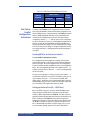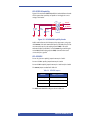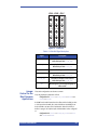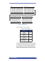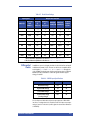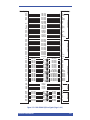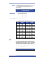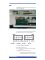
1
VERSION 0.93
October 1, 2003
ET5000k10S
User’s Manual
Version 0.93
October 1, 2003
EMULATION TECHNOLOGY, INC.
ET5000K10S USER’S MANUAL
.
The information contained within this manual and the accompanying
software program are protected by copyright; all rights are reserved by
Emulation Technology, inc.. Therewith, Emulation Technology, Inc.
reserves a the right to make periodic modifications to this project without
obligation to notify any person or entity of such revision. Copying, duplicating, selling, or otherwise distributing any part of this product without
the prior written consent of an authorized representative of Emulation
Technology, Inc. is prohibited.
2344 Walsh Avenue • Bldg. F
Santa Clara, CA 95051
www.emulation.com
[email protected]
(408) 982-0660
FAX: (408) 982-0664
Copyright ©2003 Emulation Technology, Inc.. All Rights Reserved.
EMULATION TECHNOLOGY, INC.
ET5000K10S USER’S MANUAL
TABLE OF CONTENTS
Table of Contents
Chapter 1
Getting Started
Emulation Technology, Inc. Technical Support . 1-1
Relevant Information . . . . . . . . . . . . . . . . . . . . . 1-1
Conventions . . . . . . . . . . . . . . . . . . . . . . . . . . . . . 1-2
Chapter 2
ET5000k10S Features, Overview and General
Description
ET5000k10S Features . . . . . . . . . . . . . . . . . . . . . . 2-1
ET5000k10S Description . . . . . . . . . . . . . . . . . . . 2-2
Easy Configuration via SmartMedia . . . . . . . . . . . . . . . . 2-3
FPGA — Stratix (U11, F) . . . . . . . . . . . . . . . . . . . . 2-3
Flip-Flops and LUTs . . . . . . . . . . . . . . . . . . . . . . . . . . . . . .
Embedded Memory. . . . . . . . . . . . . . . . . . . . . . . . . . . . . .
Multipliers . . . . . . . . . . . . . . . . . . . . . . . . . . . . . . . . . . . . .
I/O Issues . . . . . . . . . . . . . . . . . . . . . . . . . . . . . . . . . . . . . .
Bitstream Encryptions . . . . . . . . . . . . . . . . . . . . . . . . . . . .
2-3
2-4
2-5
2-7
2-8
µP and FPGA Configuration . . . . . . . . . . . . . . . . 2-9
The µP: Some Details. . . . . . . . . . . . . . . . . . . . . . . . . . . . . 2-9
P1: Unused µP Connections . . . . . . . . . . . . . . . . . . . . . . 2-10
ATmega128L JTAG Interface. . . . . . . . . . . . . . . . . . . . . . 2-11
Programming the ATmega128L (U8) . . . . . . . . . . . . . . . 2-12
Detailed Instructions. . . . . . . . . . . . . . . . . . . . . . . . . . . 2-12
CPLD—EPM3256A . . . . . . . . . . . . . . . . . . . . . . . . . . . . . . 2-14
Some Miscellaneous Notes on the CPLD . . . . . . . . . . . 2-16
Notes on Header P3 . . . . . . . . . . . . . . . . . . . . . . . . . . . 2-16
Fast Passive Parallel Configuration Instructions . . . . . . 2-17
Creating RBF Files for Fast Passive Parallel . . . . . . . . .
Setting up the Serial Port (P2 — RS232 Port) . . . . . . .
Creating Main Configuration File main.txt . . . . . . . . .
Starting Fast Passive Parallel Configuration . . . . . . . .
2-17
2-17
2-19
2-21
Description of Main Menu Options 2-22
SmartMedia . . . . . . . . . . . . . . . . . . . . . . . . . . . . . . . . . . . 2-23
Synthesis and Emulation Issues . . . . . . . . . . . . 2-24
Synthesis Notes . . . . . . . . . . . . . . . . . . . . . . . . . . . . . . . . 2-25
ET5000K10S USER’S MANUAL
iii
TABLE OF CONTENTS
Chapter 3
PCI
Overview. . . . . . . . . . . . . . . . . . . . . . . . . . . . . . . . 3-1
PCI Mechanical Specifications. . . . . . . . . . . . . . . . . . . . . . 3-1
Some Notes on the ET5000k10S and PCI/PCI-X . . . . . . . . 3-1
JP2: Present Signals for PCI/PCI-X . . . . . . . . . . . . . . . . . .
JP3: M66EN—66MHz Enable . . . . . . . . . . . . . . . . . . . . .
TP13: PME–, Power Management Enable . . . . . . . . . . .
JP3: PCI/PCI-X Capability . . . . . . . . . . . . . . . . . . . . . . . . .
JP3—PCIXCAP . . . . . . . . . . . . . . . . . . . . . . . . . . . . . . . . .
Chapter 4
3-4
3-5
3-5
3-6
3-6
Clocks and Clock Distribution
Functional Overview . . . . . . . . . . . . . . . . . . . . . . 4-1
Clock Grid . . . . . . . . . . . . . . . . . . . . . . . . . . . . . . . 4-2
Orientation and Description. . . . . . . . . . . . . . . . . . . . . . . 4-2
Jumper Control for the Most Common Applications . . . 4-3
Ribbon Cable: Providing an Off-Board Clock to the
ET5000k10S . . . . . . . . . . . . . . . . . . . . . . . . . . . . . . . . . . . . 4-4
Roboclock PLL Clock Buffers . . . . . . . . . . . . . . . . 4-5
Jumper Descriptions . . . . . . . . . . . . . . . . . . . . . . . . . . . . 4-5
General Control . . . . . . . . . . . . . . . . . . . . . . . . . . . . . . . . . 4-8
Feedback and Clock Multiplication . . . . . . . . . . . . . . . . . 4-9
Clock Division . . . . . . . . . . . . . . . . . . . . . . . . . . . . . . . . . . 4-9
Clock Skew. . . . . . . . . . . . . . . . . . . . . . . . . . . . . . . . . . . . 4-10
Differential Clocks . . . . . . . . . . . . . . . . . . . . . . . . . . . . . . 4-11
Useful Notes and Hints . . . . . . . . . . . . . . . . . . . . . . . . . . 4-12
Customizing the Oscillators . . . . . . . . . . . . . . . . . . . . . 4-12
ET5000k10S PCI_CLK Operation. . . . . . . . . . . . . 4-13
PCI_CLK Details . . . . . . . . . . . . . . . . . . . . . . . . . . . . . . . .
GCLKOUT . . . . . . . . . . . . . . . . . . . . . . . . . . . . . . . . . . . . .
Header Clocks . . . . . . . . . . . . . . . . . . . . . . . . . . . . . . . . .
DCLK[7](R) . . . . . . . . . . . . . . . . . . . . . . . . . . . . . . . . . . . .
Chapter 5
4-13
4-14
4-14
4-15
Memories
SSRAMs . . . . . . . . . . . . . . . . . . . . . . . . . . . . . . . . . 5-1
SSRAM Notes . . . . . . . . . . . . . . . . . . . . . . . . . . . . . . . . . . . 5-1
Pipeline, Flowthrough, ZBT . . . . . . . . . . . . . . . . . . . . . . . 5-6
SDRAM . . . . . . . . . . . . . . . . . . . . . . . . . . . . . . . . . 5-9
SDRAM On-Board Options . . . . . . . . . . . . . . . . . . . . . . . 5-11
DDR SDRAM . . . . . . . . . . . . . . . . . . . . . . . . . . . . . . . . . 5-12
iv
EMULATION TECHNOLOGY, INC.
TABLE OF CONTENTS
DDR SDRAM On-Board Options . . . . . . . . . . . . . . . . . . 5-12
Chapter 6
Power Supplies and Power Distribution
+3.3 V Power. . . . . . . . . . . . . . . . . . . . . . . . . . . . . 6-2
+2.5 V Power. . . . . . . . . . . . . . . . . . . . . . . . . . . . . 6-2
+1.5 V Power. . . . . . . . . . . . . . . . . . . . . . . . . . . . . 6-3
Stand-Alone Operation . . . . . . . . . . . . . . . . . . . . 6-3
Chapter 7
Daughter Connections to ET3k10SD—
Observation Daughter Card for 200-pin
Connectors
Purpose . . . . . . . . . . . . . . . . . . . . . . . . . . . . . . . . . 7-1
Features . . . . . . . . . . . . . . . . . . . . . . . . . . . . . . . . 7-1
Daughter Card LEDs . . . . . . . . . . . . . . . . . . . . . . . . . . . . . 7-4
Power Supply . . . . . . . . . . . . . . . . . . . . . . . . . . . . 7-4
Options. . . . . . . . . . . . . . . . . . . . . . . . . . . . . . . . . . . . . . . . 7-5
Power Rating . . . . . . . . . . . . . . . . . . . . . . . . . . . . . . . . . . . 7-5
Connector J8 . . . . . . . . . . . . . . . . . . . . . . . . . . . . . . . . . . . 7-5
LVDS . . . . . . . . . . . . . . . . . . . . . . . . . . . . . . . . . . . 7-5
Connector P5 . . . . . . . . . . . . . . . . . . . . . . . . . . . . . . . . . . . 7-6
Unbuffered I/O . . . . . . . . . . . . . . . . . . . . . . . . . . . 7-6
Connectors P2, P4 . . . . . . . . . . . . . . . . . . . . . . . . . . . . . . . 7-6
Connector P7, P1, P3 . . . . . . . . . . . . . . . . . . . . . . . . . . . . . 7-6
Buffered I/O . . . . . . . . . . . . . . . . . . . . . . . . . . . . . 7-6
Active . . . . . . . . . . . . . . . . . . . . . . . . . . . . . . . . . . . . . . . . 7-6
Passive . . . . . . . . . . . . . . . . . . . . . . . . . . . . . . . . . . . . . . . 7-6
Test Interface . . . . . . . . . . . . . . . . . . . . . . . . . . . . 7-7
Connector J1 . . . . . . . . . . . . . . . . . . . . . . . . . . . . . . . . . . . 7-7
Daughter Card I/O Connections. . . . . . . . . . . . . . 7-7
Chapter 8
Reset Schemes, LEDs, Bus Bars and 200 Pin
Connectors
Reset Schemes . . . . . . . . . . . . . . . . . . . . . . . . . . . 8-1
LEDs. . . . . . . . . . . . . . . . . . . . . . . . . . . . . . . . . . . . 8-3
Bus Bars . . . . . . . . . . . . . . . . . . . . . . . . . . . . . . . . . . . . . . . 8-4
ET5000K10S USER’S MANUAL
v
TABLE OF CONTENTS
The 200 Pin Connectors: P8 and P9 . . . . . . . . . . . 8-4
The Signals. . . . . . . . . . . . . . . . . . . . . . . . . . . . . . . . . . . . . 8-5
Chapter 9
Utilities
PCI Debug—General Pontificating . . . . . . . . . . . 9-1
PC-Based—AETEST.EXE. . . . . . . . . . . . . . . . . . . . . 9-1
AETEST Utility Installation Instructions . . . . . . . . . . . . . . 9-2
Installation Instructions for DOS . . . . . . . . . . . . . . . . . .
Installation Instructions for Windows NT . . . . . . . . . . .
Installation Instructions for Windows 2000. . . . . . . . . .
Installation Instructions for LINUX. . . . . . . . . . . . . . . . .
Installation Instructions for Solaris . . . . . . . . . . . . . . . .
Installation Instructions for Windows 98/ME . . . . . . . .
9-2
9-2
9-2
9-3
9-3
9-3
AETEST Options: Description and Definitions . . . . . . . . . 9-4
Startup . . . . . . . . . . . . . . . . . . . . . . . . . . . . . . . . . . . . . . . 9-4
AETEST Main Screen . . . . . . . . . . . . . . . . . . . . . . . . . . . . . 9-6
Options . . . . . . . . . . . . . . . . . . . . . . . . . . . . . . . . . . . . . . 9-6
PCI Menu . . . . . . . . . . . . . . . . . . . . . . . . . . . . . . . . . . . . . . 9-7
Memory Menu . . . . . . . . . . . . . . . . . . . . . . . . . . . . . . . . . . 9-9
Appendix ABerg Connector Datasheets
Appendix B ET5000k10S Schematic
vi
EMULATION TECHNOLOGY, INC.
LIST
OF
FIGURES
List of Figures
FIGURE
TITLE
PAGE
2-1
ET5000k10S Block Diagram. . . . . . . . . . . . . . . . . . . . .
2-2
2-2
General LE Diagram . . . . . . . . . . . . . . . . . . . . . . . . . .
2-4
2-3
Dual-Port Data Flows . . . . . . . . . . . . . . . . . . . . . . . . .
2-5
2-4
DSP Block Diagram . . . . . . . . . . . . . . . . . . . . . . . . . . .
2-6
2-5
Multiplier Sub-Component Block Diagram . . . . . . . .
2-7
2-6
ET5000k10SBlock Diagram of ATmega128L and
ET5000k10S Interfaces . . . . . . . . . . . . . . . . . . . . . . . .
2-10
2-7
P1: Unused µP Connections . . . . . . . . . . . . . . . . . . . .
2-11
2-8
P7 JTAG Interface . . . . . . . . . . . . . . . . . . . . . . . . . . . .
2-11
2-9
P5 Schematic . . . . . . . . . . . . . . . . . . . . . . . . . . . . . . . .
2-12
2-10
Location of P4 on the ET5000k10S . . . . . . . . . . . . . . .
2-15
2-11
P2 Serial Port Locations . . . . . . . . . . . . . . . . . . . . . . .
2-18
2-12
Delkin 32 MB 3.3 V Smart Media Card. . . . . . . . . . . .
2-24
3-1
FPGA Pin Connections for PCI Signals . . . . . . . . . . . .
3-2
3-2
PCI/PCI-X Edge Connector . . . . . . . . . . . . . . . . . . . . . .
3-3
3-3
ET5000k10S Dimensions . . . . . . . . . . . . . . . . . . . . . . .
3-4
3-4
JP2 PCI-X Present Header . . . . . . . . . . . . . . . . . . . . . .
3-5
3-5
PCI-X/M66EN Capability Header . . . . . . . . . . . . . . . . .
3-6
4-1
Clock Distribution Block Diagram . . . . . . . . . . . . . . .
4-1
4-2
Clock Grid. . . . . . . . . . . . . . . . . . . . . . . . . . . . . . . . . . .
4-3
4-3
PECL Clock Input and Termination. . . . . . . . . . . . . . .
4-4
4-4
External Ribbon Cable Connections . . . . . . . . . . . . .
4-5
4-5
Functional Diagram of Roboclock 1 and Roboclock 2
4-6
4-6
Header Layout . . . . . . . . . . . . . . . . . . . . . . . . . . . . . . .
4-7
4-7
Clock OE Pin Jumper Settings. . . . . . . . . . . . . . . . . . .
4-13
4-8
PCI_CLK PLL Circuit . . . . . . . . . . . . . . . . . . . . . . . . . . .
4-14
5-1
SSRAM 1 (U9) Bus Signals . . . . . . . . . . . . . . . . . . . . . .
5-2
5-2
SSRAM 2 (U10) Bus Signals . . . . . . . . . . . . . . . . . . . . .
5-3
5-3
SSRAM 3 (U8) Bus Signals . . . . . . . . . . . . . . . . . . . . . .
5-4
5-4
SSRAM 4 (U13) Bus Signals . . . . . . . . . . . . . . . . . . . . .
5-5
5-5
Syncburst FT. . . . . . . . . . . . . . . . . . . . . . . . . . . . . . . . .
5-7
5-6
Syncburst PL . . . . . . . . . . . . . . . . . . . . . . . . . . . . . . . .
5-7
5-7
Syncburst ZBT FT . . . . . . . . . . . . . . . . . . . . . . . . . . . . .
5-8
5-8
Syncburst ZBT PL . . . . . . . . . . . . . . . . . . . . . . . . . . . . .
5-8
5-9
Syncburst and ZBT SSRAM Timing . . . . . . . . . . . . . . .
5-8
5-10
SDRAM (J19) Bus Signals (Page 1 of 2) . . . . . . . . . . .
5-10
5-11
SDRAM (J19) Bus Signals (Page 2 of 2) . . . . . . . . . . .
5-11
ET5000K10S USER’S MANUAL
vii
LIST
OF
FIGURES
List of Figures (Continued)
FIGURE
viii
TITLE
PAGE
5-12
DDR SDRAM (J2) Bus Signals (Page 1 of 2) . . . . . . . .
5-13
5-13
DDR SDRAM (J2) Bus Signals (Page 2 of 2) . . . . . . . .
5-14
5-14
DDR PLL Circuit Block Diagram . . . . . . . . . . . . . . . . .
5-15
5-15
DDR Clock Select Jumper (JP4) . . . . . . . . . . . . . . . . . .
5-15
6-1
ET5000k10S Power Distribution . . . . . . . . . . . . . . . . .
6-1
6-2
Molex Connector P1—Auxiliary Power . . . . . . . . . . .
6-4
6-3
Example ATX Power Supply . . . . . . . . . . . . . . . . . . . .
6-4
7-1
ET3k10SD Daughter Card Block Diagram . . . . . . . . .
7-2
7-2
ET3k10SD Daughter Card . . . . . . . . . . . . . . . . . . . . . .
7-3
7-3
ET3k10SD Daughter Card Assembly Drawing . . . . . .
7-4
8-1
Reset Functionality . . . . . . . . . . . . . . . . . . . . . . . . . . .
8-2
8-2
ET5000k10S LEDs . . . . . . . . . . . . . . . . . . . . . . . . . . . . .
8-3
8-3
ET5000k10S LED Diagram . . . . . . . . . . . . . . . . . . . . . .
8-3
8-4
91294-003 Pin Numbering. . . . . . . . . . . . . . . . . . . . . .
8-5
8-5
200-Pin Connectors — Signal Connections . . . . . . . .
8-7
9-1
ET5000k10SAETEST Startup Screen, ET5000k10S
Recognized. . . . . . . . . . . . . . . . . . . . . . . . . . . . . . . . . .
9-4
9-2
AETEST Startup Screen, No PCI Peripheral Recognized
9-5
9-3
AETEST Main Screen . . . . . . . . . . . . . . . . . . . . . . . . . .
9-6
9-4
AETEST PCI Menu . . . . . . . . . . . . . . . . . . . . . . . . . . . . .
9-7
9-5
AETEST Memory Menu . . . . . . . . . . . . . . . . . . . . . . . .
9-9
9-6
AETEST Write to Memory Test . . . . . . . . . . . . . . . . . .
9-10
9-7
AETEST Read Memory Test . . . . . . . . . . . . . . . . . . . . .
9-10
9-8
AETEST Write/Read Test . . . . . . . . . . . . . . . . . . . . . . .
9-11
9-9
AETEST Memory Fill. . . . . . . . . . . . . . . . . . . . . . . . . . .
9-11
9-10
AETEST Memory Display . . . . . . . . . . . . . . . . . . . . . . .
9-12
9-11
AETEST Write/Read Memory Byte. . . . . . . . . . . . . . . .
9-13
A-1
Berg 91403-003 Datasheet Page 1 of 2 . . . . . . . . . . .
A-2
A-2
Berg 91403-003 Datasheet Page 2 of 2 . . . . . . . . . . .
A-3
A-3
Berg 91294-003 Datasheet Page 1 of 3 . . . . . . . . . . .
A-4
A-4
Berg 91294-003 Datasheet Page 2 of 3 . . . . . . . . . . .
A-5
A-5
Berg 91294-003 Datasheet Page 3 of 3 . . . . . . . . . . .
A-6
EMULATION TECHNOLOGY, INC.
LIST
OF
TABLES
List of Tables
TABLE
TITLE
PAGE
2-1
ET5000k10S Stuffing Option Comparison . . . . . . . . .
2-3
2-2
Signals and Connections to P4 . . . . . . . . . . . . . . . . . .
2-15
2-3
FPGA Serial/JTAG Configuration Header . . . . . . . . . .
2-16
2-4
JP1 Configuration Jumper Settings . . . . . . . . . . . . . .
2-21
2-5
Stratix FPGA Approximate File Sizes . . . . . . . . . . . . .
2-23
3-1
Present Signal Definitions . . . . . . . . . . . . . . . . . . . . .
3-5
3-2
M66EN Jumper Descriptions. . . . . . . . . . . . . . . . . . . .
3-5
3-3
PCIXCAP Jumpers . . . . . . . . . . . . . . . . . . . . . . . . . . . .
3-6
3-4
M66EN and PCIXCAP Encoding . . . . . . . . . . . . . . . . . .
3-7
4-1
Clock Grid Signal Descriptions . . . . . . . . . . . . . . . . . .
4-2
4-2
Header Classification . . . . . . . . . . . . . . . . . . . . . . . . .
4-7
4-3
Jumper Definitions . . . . . . . . . . . . . . . . . . . . . . . . . . .
4-8
4-4
Frequency Range Settings . . . . . . . . . . . . . . . . . . . . .
4-9
4-5
Output Divider Settings . . . . . . . . . . . . . . . . . . . . . . .
4-9
4-6
Time Unit N-factor . . . . . . . . . . . . . . . . . . . . . . . . . . . .
4-10
4-7
Clock Skew Settings . . . . . . . . . . . . . . . . . . . . . . . . . .
4-11
4-8
LVPECL Input Specifications . . . . . . . . . . . . . . . . . . . .
4-11
4-9
Clock OE Pin Jumper Settings. . . . . . . . . . . . . . . . . . .
4-13
5-1
Requirements for Non-Standard SSRAMs . . . . . . . . .
5-6
5-2
Syncburst and ZBT SSRAM Timing . . . . . . . . . . . . . . .
5-9
6-1
Specification for +3.3 V Power . . . . . . . . . . . . . . . . . .
6-2
6-2
Specification for +2.5 V Power and +1.25 V Reference
6-3
6-3
Specification for +1.5 V Power . . . . . . . . . . . . . . . . . .
6-3
7-1
Connector J8 Pins External Power . . . . . . . . . . . . . . .
7-5
7-2
Daughter Board-Header-FPGA Pin Map . . . . . . . . . . .
7-7
ET5000K10S USER’S MANUAL
ix
EMULATION TECHNOLOGY, INC.
Chapter 1
Getting Started
The ET5000k10S is sensitive to static electricity, so treat the PWB accordingly. The target market for this product is engineers that are familiar with
FPGAs and circuit boards, so a lecture in ESD really isn’t appropriate (and
wouldn’t be read anyway). However, we have sold some of these units to
people who are not as familiar with this issue. The following web page has
an excellent tutorial on the Fundamentals of ESD for those of you who are
new to ESD-sensitive products:
http://www.esda.org/basics/part1.cfm.
Emulation Technology, Inc. Technical Support
The following means of technical support are available:
1. The ET5000k10S User’s Manual. This is the main source of technical
information. We strive to produce excellent documentation, and this
manual should contain most of the answers to your questions.
2. The Emulation Technology Web Page. The web page will contain the
latest manual, application notes, faq, articles, and any device errata
and manual addenda. Please visit and bookmark:
http://www.emulation.com.
3. E-Mail to [email protected]. You may direct questions and
feedback to Emulation Technology using this e-mail address.
4. Phone Support. We are happy to help. Call us at 1-800-ADAPTER
during the hours of 8:00 A.M. to 5:00 P.M. Pacific Time. Some of us get
in early and stay late, so you might try us outside of these hours also.
5. Frequently Asked Questions. In the downloads section of our web
page you can find a document called ET5000k10/S Frequently Asked
Questions (FAQ). We will update this document occasionally with
information that may not be in the User’s Manual.
Relevant Information
Information about PCI can be obtained from the following sources:
The PCI Special Interest Group has a web page that has lots of good stuff.
Copies of the latest PCI specification may be ordered here.
http://www.pcisig.com/
PCI Special Interest Group
2575 NE Kathryn St. #17
Hillsboro, OR 97124
FAX: (503) 693-8344
ET5000K10S USER’S MANUAL
1–1
GETTING STARTED
As of June 2003, the most current versions of the PCI Specifications are:
PCI Local Bus Specification, Revision 3.0
PCI Hot-Plug Specification, Revision 2.0
PCI Power Management Interface Specification, Revision 1.1
PCI-X Addendum to the PCI Local Bus Specification, Revision 1.0a
Other recommended specifications include:
PCIMG 2.0 Compact PCI Specification, Revision 2.1 (or greater)
PCI Industrial Computer Manufacturers Group (PICMG)
401 Edgewater Place, Suite 500
Wakefield, MA 01880, USA
TEL: 781-224-1100
FAX: 781-224-1239
http://www.picmg.org
The best book to get if you need an introduction to PCI is:
PCI System Architecture
Fourth Edition
MindShare, Inc.
Tom Shanley and Don Anderson
Ignore some of the ignorant statements made in the Customer Review
section at http://www.amazon.com/. This is an excellent book for PCI and
well worth the money.
The best book to get if you need an introduction to PCI-X is:
PCI-X System Architecture
MindShare, Inc.
Tom Shanely and Karen Gettman
You are going to need to know Verilog or VHDL to use the Stratix FPGA. If
you need a reference, we recommend the following book for Verilog:
Verilog HDL: A Guide to Digital Design and Synthesis
Samir Palnitkar
ISBN: 0-13-451675-3
If you are one of those people that actually like VHDL, we feel sorry for
you. The following books may be helpful:
Essential VHDL: RTL Synthesis Done Right
Sundar Rajan
The IQ Booster: Improve Your IQ Performance Dramatically
Edwin Breecher
Conventions
This manual uses the following conventions. An example illustrates each
convention.
1–2
•
The term PCI-X will be used generically unless there is a specific
instance where PCI applies.
•
This design guide generically refers to PCI-X protocol.
EMULATION TECHNOLOGY, INC.
GETTING STARTED
•
Courier font denotes the following items:
–
Signals on PCI Bus side of the PCI-X Interface
FRAME_IO (PCI-X Interface signal name)
FRAME# (PCI-X Bus signal name)
–
Signals within the user application
BACK_UP, START
–
Command line input and output
setenv XIL_MAP_LOC_CLOSED
–
HDL pseudocode
assign question = to_be | !to_be;
assign cannot = have_cake & eat_it;
–
Design file names
pcim_top.v, pcim_top.vhd
•
Courier bold denotes the following items:
–
Signals on the user side of the LogiCORE PCI-X Interface
ADDR_VLD
–
Menu selections or button presses
FILE -> OPEN
•
Italic font denotes the following items:
–
Variables in statements which require user-supplied values
ngdbuild design_name
–
References to other manuals
See the Libraries Guide for more information.
–
Emphasis in text
It is not a bug, it is a feature.
•
Dark shading indicates items that are not supported or reserved:
SDONE_I
•
in/out
Snoop Done signal. Not
Supported.
Square brackets “[ ]” indicate an optional entry or a bus index:
ngdbuild [option_name] design_name
ET5000K10S USER’S MANUAL
1–3
GETTING STARTED
DATA[31:0]
•
A vertical or horizontal ellipsis indicates repetitive material that
has been omitted.
A B C... X Y Z
•
The use of “fn(SIG1. . . SIGn)” in an HDL pseudocode fragment should be interpreted as “combinational function of signals
SIG1 through SIGn.
SUM = fn(A, B, Cin);
•
The prefix “0x” or the suffix “h” indicate hexadecimal notation.
A read of address 0x00110373 returned 45524943h.
•
A “#” an “_n” , an “n” or a “–” means the signal is active low
INT# is active low.
fpga_inta_n is active low.
SRAMCS– is active low.
FPGA_GRSTn is active low.
1–4
EMULATION TECHNOLOGY, INC.
ET5000K10S FEATURES, OVERVIEW AND GENERAL DESCRIPTION
Chapter 2
ET5000k10S Features, Overview and General
Description
ET5000k10S Features
The ET5000k10S features include:
•
32/64-bit, +3.3V, PCI/PCI-X-based PWB with a single Altera Stratix™
FPGA (FBGA1508).
–
Device availability: EP1S80, EP1S60 and EP1S40
–
~450,000 ASIC gates (with EP1S80 — LSI standard)
Embedded Memory
Device
I/O
Flip-Flops
18 x 18 Multipliers
M512 RAM
M4K RAM
M-RAM
EP1S40
822
41,250
56
384
183
4
EP1S60
1022
57,120
72
574
292
6
EP1S80
1203
79,040
88
767
364
9
•
Fast/Easy FPGA configuration via standard SmartMedia FLASH card
–
–
–
•
Microprocessor controlled (ATmega128L)
RS232 port for configuration/operation status and control
Fastest possible configuration speed (via Passive Parallel
method)
10A on-board linear regulator for +3.3V and +1.5V
–
–
•
6 low skew clocks distributed to the FPGA and test connectors:
–
–
–
–
ET5000K10S USER’S MANUAL
Standalone operation via separate power connector
+3.3V not needed on backplane
2 CY7B993/4 RoboclockII PLLs
2 socketed oscillators
PCI Clock
1 dividable clock via CPLD
•
Robust observation/debug with 242 connections for logic
analyzer observability or for pattern generator stimulus.
•
Status LEDs.
•
User-designed daughter PWB for custom circuitry and interfaces.
2–1
ET5000K10S FEATURES, OVERVIEW AND GENERAL DESCRIPTION
•
SignalTap and Identify (from Synplicity) fully supported via JTAG
interface.
Figure 2-1 shows a block diagram of the ET5000k10S.
ET5000k10S Description
The ET5000k10S is a complete logic emulation system that enables ASIC or
IP designers a vehicle to prototype logic and memory designs for a fraction
of the cost of existing solutions. The ET5000k10S can be hosted in a 32/64bit PCI/PCI-X slot, or can be used as a stand-alone device. A single
ET5000k10S stuffed with a single EP1S80 can emulate up to 450,000 gates
of logic as measured by LSI. A high I/O-count, 1508-pin, flip-chip BGA
package is employed. The F1508 package has 1203 I/Os, which allows for
abundant connections to daughter connectors and external memories. A
total of 242 test pins are provided on the top of the PWB via high-density
connectors for logic analyzer-based debugging, or for pattern generator
stimulus. Custom daughter cards such as the ET3k10SD can be mounted to
these connectors as a means of interfacing the ET5000k10S to applicationspecific circuits. A reference 32-bit PCI target design and test bench is
provided in Verilog and VHDL at no additional cost.
+5V
-12V
Smart Media
Card
16/32/64 Mbyte
32kx8 SRAM
(FPGA configuration
storage)
+3.3V
+3.3V
+2.5V
+1.5V
ATmega103L
Flash-based µP
FPGA
Configuration
Controller
2
RS232
+12V
3256A
CPLD
Top of PWB
Power
Monitor
+5V
+1.5V
Reset
Control
(test connectors)
FPGA CONFIGURATION
JTAG
Connector
Aux Power
Connector
+2.5V
+12V
242
+3.3V
address
21
+1.5V
data
36
control
+5V
+5V
ACLK
Switching +3.3V (5A)
Regulator
+1.5V (5A)
Regulator
POWER
ACLK
BCLK
config
BCLK
CCLK
DCLK
ECLK
Altera Stratix
FPGA
EP1S40/60/80
(BGA 1508)
address
21
data
36
control
21
data
36
21
data
36
control
512k x 36
FlowThrough/
Pipelined
512k x 36
FlowThrough/
Pipelined
OSC
X2
Clock
Selection
Jumpers
or
External
Cable
Roboclock
PLL
1
Roboclock
PLL
2
512k x 36
FlowThrough/
Pipelined
ECLK
SSRAM
14
512k x 36
CCLK
SDRAM
ECLK
(168 pin DIMM Module)
Up to 2GB x 72
DCLK
125
ECLK
DDR
FCLK
(168 pin DIMM Module)
92
config
ECLK
SSRAM
100
OSC
X1
ECLK
SSRAM
14
address
ECLK
SSRAM
14
address
control
FlowThrough/
Pipelined
14
CLOCKS
32/64-Bit PCI/PCI-X
Rev 5/30/03
Figure 2-1 ET5000k10S Block Diagram
2–2
EMULATION TECHNOLOGY, INC.
ET5000K10S FEATURES, OVERVIEW AND GENERAL DESCRIPTION
Easy
Configuration
via
SmartMedia
The configuration bit files for the FPGA are copied onto a 32-megabyte
SmartMedia FLASH card (provided) and an on-board microprocessor
controls the FPGA configuration process. Visibility into the configuration
process is enhanced with an RS232 port. FPGA configuration runs quickly
at 48 MHz. Eight LEDs provide instant status and operational feedback.
Four of these LEDs are connected to the CPLD and can be user-configured.
FPGA — Stratix (U11, F)
The ET5000k10S contains one Stratix™ FPGA. The package is a flip chip
fine-pitch BGA with 1508 pins (F1508). The pitch on the pins is 1 mm. This
isn’t important, but this pin density makes the PWB a bitch to layout. Keep
that in mind if you try to make one of these at home. Most of the 1203 I/O
pins are utilized on the F1508 package. The standard speed grade we stuff
is –7. We can use the –6 speed grade, but don’t fall out of your chair when
you get the price. Note that Altera seems to have cancelled plans for the
EP1S120. Although this part appears in some Altera literature, we haven’t
seen any scheduled release date or other documentation for it. Don’t
expect to see anything larger than the EP1S80 until at least the 2004 time
frame. Table 2-1 shows the stuffing options for the ET5000k10S.
Table 2-1 ET5000k10S Stuffing Option Comparison
Stuffed FPGA
SSRAMs
SDRAM
DDR
SDRAM
Total Header
Connections
EP1S40_1508
3
1
1
77
EP1S60_1508
3
1
1
180
EP1S80_1508
4
1
1
242
The following is a very brief overview of the Stratix family. More information can be gleaned from the Stratix Datasheet (ds_stx.pdf). This file is
on the CD-ROM supplied with the ET5000k10S, but you are better off
getting the latest version from the Altera Web page
(http://www.altera.com/). Make sure to get the latest errata sheet also.
Flip-Flops and
LUTs
Figure 2-2 shows what Altera calls a Logic Element, or LE. Each LE contains
a flip-flop and a 4x1 look-up table (LUT). LEs are arranged in groups of 10,
called Logic Array Blocks (LAB). The EP1S80 is an array of LABs with 91
rows and 101 columns, but there are 9 RAM blocks which appear in place
of 13-row by 11-column sections of the grid, leaving a total of 7904 LABs
and 19040 LEs. (Other blocks, such as DSP/multiplier blocks and smaller
RAM, are arranged in entire columns squeezed between two LAB columns.)
Each LUT can implement any Boolean function of four inputs. An LUT can
also be configured as a two-input adder/subtractor with a carry chain
coming from the adjacent LE and going to the next LE. In order to reduce
delays caused by long carry chains, each set of 5 LEs computes two adder
ET5000K10S USER’S MANUAL
2–3
ET5000K10S FEATURES, OVERVIEW AND GENERAL DESCRIPTION
results simultaneously, then uses the carry result from the previous set of
5 to select which result is correct.
The flip-flop in each LE includes a clock enable input, an asynchronous
preset and reset, synchronous set and reset logic, and an asynchronous
load function. Data input can come from the LUT in the same LE to register
addition or boolean outputs, or the LUT and flip-flop can be used independently of each other. For more information, check www.altera.com for
the Stratix datasheet.
Embedded
Memory
Stratix has boatloads of embedded memory. The EP1S80 contains 767
blocks of 576 bits, 364 blocks of 4.5 Kbits, and 9 blocks of 576 Kbits. The
smallest memory blocks (called M512 RAM) can be configured for data
widths ranging from 32 x 18 bits to 512 x 1 bit; medium-sized blocks (M4K
RAM) can be configured ranging from 128 x 36 bits to 4K x 1 bit; and the
largest blocks (M-RAM) can be configured anywhere from 4K x 144 bits to
64K x 9 bits. The embedded memory is dual-ported, and can be used to
construct almost any type of memory - FIFOs, dual-port RAMs, single-port
RAMs, etc.
The two largest blocks, M-RAM and M4K RAM, are fully dual-ported
memory, with read and write functions available on two separately
clocked ports. M512 RAM is a “simple dual-port” memory, meaning that
Register chain
routing from
previous LE
LAB-wide
Register Bypass
Synchronous
Load
LAB-wide
Packed
Synchronous
Register Select
Clear
LAB Carry-In
addnsub
Carry-In1
Carry-In0
Programmable
Register
LUT chain
routing to next LE
data1
data2
data3
Look-Up
Table
(LUT)
Carry
Chain
Synchronous
Load and
Clear Logic
PRN/ALD
D
Q
ADATA
Row, column,
and direct link
routing
data4
ENA
CLRN
labclr1
labclr2
labpre/aload
Chip-Wide
Reset
Asynchronous
Clear/Preset/
Load Logic
Row, column,
and direct link
routing
Local Routing
Clock &
Clock Enable
Select
Register
Feedback
Register chain
output
labclk1
labclk2
labclkena1
labclkena2
Carry-Out0
Carry-Out1
LAB Carry-Out
Figure 2-2 General LE Diagram
2–4
EMULATION TECHNOLOGY, INC.
ET5000K10S FEATURES, OVERVIEW AND GENERAL DESCRIPTION
one port is write-only and the other is read-only. Any of the memory
blocks can be configured as simple dual-port or single-port memory. See
Figure 2-3 for a diagram of the memory.
Multipliers
Stratix devices feature a large number of multipliers grouped into what
Altera calls DSP blocks (see Figure 2-4). The EP1S80 contains 22 DSP blocks,
each of which can provide one 36x36 bit multiplier, four 18x18 bit multipliers, or eight 9x9 bit multipliers. Each block also contains adder/
subtractor/accumulator registers which can be configured to provide
many common DSP functions, such as FIR or IIR filters, FFT, or DCT, without
the use of LAB resources. The Stratix datasheet (available at
www.altera.com) has more detailed information on how the multipliers
and adders are configured for some common functions.
Figure 2-4 shows a DSP block configured for four 18x18 bit multipliers. A
DSP block can be configured as two parallel systems of 9x9 bit multipliers,
each of which is also described by Figure 2-4. The adder blocks can be used
to add or subtract two or four multipliers, such as in complex multiplication, or to add a new result each clock cycle to an accumulated sum. They
are also used to configure the DSP block as a 36x36 bit multiplier, with or
without an accumulator.
All registers in Figure 2-4 are optional, as shown by Figure 2-5, which is a
detailed view of a single 18x18 bit or 9x9 bit multiplier. Any or all of the
registers may be used to pipeline the multiplier logic and improve the
clock speed, or the alternate path may be used to bypass the register.
ALTQPRAM
rdaddress_a[]
rden_a
q_a[]
outclock_a
outclocken_a
data_a[]
wraddress_a[]
wren_a
inclock_a
inclocken_a
rdaddress_b[]
rden_b
q_b[]
outclock_b
outclocken_b
inaclr_b
outaclr_b
inclock_b
inclocken_b
inaclr_a
outaclr_a
data_b[]
wraddress_b[]
wren_b
inst
Figure 2-3 Dual-Port Data Flows
ET5000K10S USER’S MANUAL
2–5
ET5000K10S FEATURES, OVERVIEW AND GENERAL DESCRIPTION
Optional Serial Shift Register
Inputs from Previous
DSP Block
Multiplier Stage
D
Optional Stage Configurable
as Accumulator or Dynamic
Adder/Subtractor
Q
ENA
CLRN
D
D
ENA
CLRN
Q
Output Selection
Multiplexer
Q
ENA
CLRN
Adder/
Subtractor/
Accumulator
1
D
Q
ENA
CLRN
D
D
ENA
CLRN
Q
Q
ENA
CLRN
Summation
D
Q
ENA
CLRN
D
Q
D
Q
Summation Stage
for Adding Four
Multipliers Together
ENA
CLRN
Optional Output
Register Stage
ENA
CLRN
Adder/
Subtractor/
Accumulator
2
D
Optional Serial
Shift Register
Outputs to
Next DSP Block
in the Column
Q
ENA
CLRN
D
D
ENA
CLRN
Q
ENA
CLRN
Q
Optional Pipeline
Register Stage
Optional Input Register
Stage with Parallel Input or
Shift Register Configuration
to MultiTrack
Interconnect
Figure 2-4 DSP Block Diagram
2–6
EMULATION TECHNOLOGY, INC.
ET5000K10S FEATURES, OVERVIEW AND GENERAL DESCRIPTION
Figure 2-5 also shows more detail about the optional shift register path,
which makes FIR or IIR filters easy to implement.
Most synthesis tools will accept Verilog or VHDL descriptions of multpliers
and infer a DSP block with the appropriate configuration. For those that
don't, Altera provides a megafunction generator to help with direct
instantiation of the hardware resources. See “Synthesis and Emulation
Issues” on page 24 for more detail.
I/O Issues
Terminator technology is supported on all pins. The resistors used for RDN
and RUP should be 250 ohms for series termination or impedance
matching I/O standards. Parallel termination requires 1000 ohm resistors
for RDN and RUP. Terminator technology is a very nice feature and we
recommend you use it on all I/O signals. The default IO_STANDARD
attribute for the .csf file is LVTLL.
All VCCO pins are connected to either +3.3 V or +2.5 V. The VREF pins are
connected to +1.5 V or +2.5 V, so the ET5000k10S does not support I/O
standards that require other values of VREF. So the I/O standards supported
are:
LVTTL — Low-Voltage TTL
The low-voltage TTL, or LVTTL, standard is a general-purpose EIA/JESDSA
sign_a (1)
sign_b (1)
aclr[3..0]
clock[3..0]
ena[3..0]
shiftin A
shiftin B
D
Data A
Q
ENA
CLRN
D
ENA
Q
CLRN
D
Data B
Q
ENA
Result
to Adder
blocks
Optional
Multiply-Accumulate
and Multiply-Add
Pipeline
CLRN
shiftout B
shiftout A
Figure 2-5 Multiplier Sub-Component Block Diagram
ET5000K10S USER’S MANUAL
2–7
ET5000K10S FEATURES, OVERVIEW AND GENERAL DESCRIPTION
standard for 3.3 V applications that use the LVTTL input buffer and a PushPull output buffer. The standard requires a 3.3 V input and output source
voltage (VCCO) but does not require the use of a reference voltage (VREF)
or a termination voltage (VTT).
LVCMOS33 — 3.3 Volt Low-Voltage CMOS
This standard is an extension of the LVCMOS standard (JESD8. –5). It is used
in general-purpose 3.3 V applications. The standard requires a 3.3 V
input/output source voltage (VCCO) but does not require the use of a reference voltage (VREF) or a termination voltage (VTT).
PCI-X — Peripheral Component Interface
The PCI standard specifies support for 33 MHz, 66 MHz and 133 MHz PCI
bus applications. It uses a LVTTL input buffer and a Push-Pull output buffer.
This standard does not require the use of a reference voltage (VREF) or a
board termination voltage (VTT); however, it does require 3.3 V input
output source voltage (VCCO).
SSTL-3 class I and II
SSTL-3 uses a series termination resistor on output signals and a parallel
termination resistor on input signals. Stratix devices use a VREF of +1.5V
to enable the appropriate resistors internally. Because SSTL-3 requires
parallel termination, it is only available on banks 3, 4, 7 and 8, and on clock
output signals.
CTT
CTT uses a parallel termination resistor on input signals, with no termination resistors on output signals. Stratix devices use a VREF of +1.5V to
enable the appropriate resistors internally. Because CTT requires parallel
termination, it is only available on I/O banks 3, 4, 7 and 8, and on clock
output signals.
SSTL-2 Class I & II
The SSTL-2 I/O standard is a 2.5-V memory bus standard used for applications such as high-speed DDR SDRAM interfaces. This standard defines the
input and output specifications for devices that operate in the SSTL-2 logic
switching range of 0.0 to 2.5 V. This standard improves operation in conditions where a bus must be isolated from large stubs.
Differential SSTL-2
The differential SSTL-2 I/O standard is a 2.5-V standard used for applications such as high-speed DDR SDRAM clock interfaces. This standard
supports differential signals in systems using the SSTL-2 standard and
supplements the SSTL-2 standard for differential clocks. The differential
SSTL-2 standard does not require an input reference voltage differential.
Bitstream
Encryptions
2–8
Stratix devices have no special bitstream encryption function. Emulation
Technology, Inc. may be able to assist with scrambling bitfiles to protect IP
on the SmartMedia card, which would then be descrambled in the
programming CPLD. Users should be aware, however, that the bitstream
would be unprotected between the CPLD and FPGA, so they could still be
examined and reverse-engineered. Our ET3000k10 products use Xilinx
FPGAs which can be used to decrypt the bitstream inside the FPGA,
EMULATION TECHNOLOGY, INC.
ET5000K10S FEATURES, OVERVIEW AND GENERAL DESCRIPTION
providing complete design protection. If you are interested in this
feature, please be aware that there are some issues with the Xilinx encryption feature, described in the ET3000k10 FAQ on our website.
µP and FPGA Configuration
The ET5000k10S has an ATmega128L microprocessor (µP) that is used to
control the configuration process (U4). The amount of internal SRAM
(4 Kbytes) was not large enough to hold the FAT needed for SmartMedia,
so an external 32 k x 8 SRAM was added. The address latching function is
done via an LVT373 (U1).
The microprocessor has the following responsibilities:
•
Reading the SmartMedia card
•
Configuring the Stratix FPGA
•
Executing ET5000k10S self tests.
Other than FPGA configuration, the µP has no responsibilities. Less than
25% of the 128 Kbytes of FLASH is used for FPGA configuration and utilities, so you are welcome to use the rest of the resources of the µP for your
own purposes. Instructions for customizing the µP are contained in the file
Custom_ATmega128L.pdf. This file is on the cd-rom, or it can be downloaded from the Emulation Technology, Inc. web page.
REMEMBER: You can use the microprocessor for your own
purposes!
We ship a programming cable for the ATmega128L with the ET5000k10S.
Updates to the code will be posted on our web site. If you wish to do your
own development you will need the compiler, which we do not ship with
the product. The compiler is available from IAR (http://www.iar.com/).
The part number is EWA90PCUBLV150.
Note that if you are willing to program the FPGA with the JTAG or serial
cable, the CLPD and the µP have no function. In this case you can use all of
the resources of the µP for your own purposes.
The µP: Some
Details
The ATmega128L is gross overkill for the FPGA configuration function. The
datasheet and user’s manual are on the CD-ROM that was shipped with the
ET5000k10S. The file names are ATmega128_UM.pdf and
ATmega128_DS.pdf. But if you intend to use the µP for your own
purposes, you should check the Atmel web page to get a copy of the latest
user’s manual, datasheet, and erratas. The Atmel web page is
http://www.eu.atmel.com/atmel/. The ATmega128L is under the section
called “Flash Microcontroller, AVR 8-Bit RISC.” Most of the features are
unused. A variety of test headers allow for possible use of these features.
Each header and the various possible functions are described in the
sections that follow. Figure 2-6 is a block diagram of the ATmega128L and
its various interfaces on the ET5000k10S.
ET5000K10S USER’S MANUAL
2–9
ET5000K10S FEATURES, OVERVIEW AND GENERAL DESCRIPTION
CSF*
+3.3V
Noise
Conditioner
A/D Inputs or
User I/O
µP
AREF
JTAG
AVCC
FWRTSM
General
Purpose I/O
DOUTBSYF
D [7:0]
P1
P7
(U11)
WR*
A/D
JP1
Config.
Jumpers
JMPR [2:0]
RD*
Atmel AVR
ATmega128L
RS232
Level
Translator
P2
Tx
RS232
Connector
Rx
ICL3221
FPGA
F
ALE
µP
µPADDR [14:8]
µPAD[7:0]
128kbytes FLASH
4kbytes SRAM
4kbytes EEPROM
U4
SRAM
32kx8
Smart
Media
EPM3256A
µPADDR[7:0]
U7
CPLD
U6
8 MHz
Card
Inserted
PWR RST-
+5V
+3.3V
+1.5V
Programming
Header
P5
U5
Reset & Power
Threshold Detection
DS2
LED[3:0]
4
Reset
Switch
S1
X1
48MHz
Osc
4
P4
Programming
Header
DS1
uP_LED[3:0]
Rev 5/30/03
Figure 2-6 ET5000k10SBlock Diagram of ATmega128L and ET5000k10S Interfaces
P1: Unused µP
Connections
P1 contains connections to the ATmega128L that were not used elsewhere. These ten connections can be used for external TTL connections to
the µP, externally generated interrupts, or any other function that the
ATmega128L supports on these pins. Remember that the ATmega128L is
not +5 V tolerant, so if you attach external TTL signals to these pins, the
voltage level of these signals must not exceed +3.3 V.
The P1 schematic is shown in Figure 2-7.
2–10
EMULATION TECHNOLOGY, INC.
ET5000K10S FEATURES, OVERVIEW AND GENERAL DESCRIPTION
µP GPIO
P1
P_D2
P_D4
P_D6
MISO
MOSI
1
3
5
7
9
2
4
6
8
10
P_D3
P_D5
P_D7
SSn
SM_CDn
SM_WP1n
P_D2
P_D3
P_D4
P_D5
P_D6
P_D7
25
26
27
28
29
30
31
32
PD0/INT0
PD1/INT1
PD2/INT2
PD3/INT3
PD4/IC1
PD5
PD6/T1
PD7/T2
Figure 2-7 P1: Unused µP Connections
µP JTAG
+3.3V
+3.3V
R63
(0)
P7
PF4
PF6
PF5
PF7
1
3
5
7
9
2
4
6
8
10
PWRRSTn
PF4
PF5
PF6
PF7
61
60
59
58
57
56
55
54
PF0/ADC0
PF1/ADC1
PF2/ADC2
PF3/ADC3
PF4/ADC4
PF5/ADC5
PF6/ADC6
PF7/ADC7
Figure 2-8 P7 JTAG Interface
ATmega128L
JTAG Interface
The ATmega128L processor has a JTAG interface that can be used for onchip debugging, real-time emulation, and programming of FLASH,
EEPROM, fuses, and Lock Bits. In order to take advantage of the JTAG interface, you must have the Atmel AVR JTAG ICE kit (part number ATAVRJTAGICE) and AVR studio software that Atmel provides free at
ET5000K10S USER’S MANUAL
2–11
ET5000K10S FEATURES, OVERVIEW AND GENERAL DESCRIPTION
www.atmel.com. The JTAG interface for the ATmega128L can be accessed
through header P7 of the ET5000k10S (see Figure 2-8).
Programming
the
ATmega128L
(U8)
A cable used to reprogram the ATmega128L is shipped with the
ET5000k10S. You will need to reprogram the ATmega128L if we update
the code or you intend to use the processor for your own application. P5
is used for this purpose.
Figure 2-9 illustrates P5.
+3.3V
ISP
R117
0
P5
BRXD
PWRRSTn
SCK
BTXD
1
3
5
7
9
2
4
6
8
10
Figure 2-9 P5 Schematic
Detailed Instructions
1. Download the latest update for the processor and CPLD at
www.emulation.com (file uP_CPLD.zip).
2. You will first need to reprogram the CPLD. Please see “CPLD—
EPM3256A” on page 14 for instructions (use the file *.jed that can
be found in the downloaded zip file.
3. Next, you will program the processor (ATmetga128L). Connect the
AVR cable that was shipped with the ET5000k10S to header P5 with
the red/purple wire on the cable connected to pin 1 and connect the
other end to the serial port of your PC.
4. In order to program the processor, you will need to install AVR Studio
that is included on the CD that was shipped with the ET5000k10S. This
software can also be downloaded at www.atmel.com.
5. From the Windows START menu, choose PROGRAMS–>Atmel AVR Studio x.xx (where x.xx is the version number).
6. Once AVR Studio is open, select TOOLS–>STK500/AVRISP/JTAG ICE and
a new window should appear with the title STK500. At the bottom of
the STK500 window, if you see:
Detecting…FAILED!
that means either there is no power on the ET5000k10S, there is
another program open that is using the serial port, or the serial cable
connecting the AVR tool is not connected properly. If this happens,
2–12
EMULATION TECHNOLOGY, INC.
ET5000K10S FEATURES, OVERVIEW AND GENERAL DESCRIPTION
you should close down the window titled STK500, correct the situation, and then select TOOLS–>STK500/AVRISP/JTAG ICE again. You
will not be able to continue unless you see something very similar to
the following at the bottom of the STK500 window:
Detecting…AVRISP found on COM1:
Getting revisions…HW: 0x01, SW Major: 0x01, SW
Minor: 0x07…OK
7. On the PROGRAM tab, select the ATmega128 under the DEVICE drop
down menu, and in the FLASH section where it says INPUT HEX FILE,
browse and select the file ET5000k10S_128.a90 that can be found
in the downloaded zip file (uP_CPLD.zip) from the Emulation
Technology, Inc. website. To program the device all you need to do is
hit the PROGRAM button in the FLASH section. When the programming is complete (it takes about 45 seconds) you should see a message at the bottom of the window that looks something like this:
Detecting…AVRISP found on COM1:
Getting revisions…HW: 0x01, SW Major 0x01, SW
Minor: 0x07…OK
Reading FLASH input file…OK
Setting device parameters, serial programming
mode…OK
Entering programming mode…OK
Erasing device…OK
Programming FLASH using block mode…100% OK
Leaving programming mode…OK
8. After programming the processor, close all AVR Studio windows and
setup the serial port according to the section titled “Setting up the
Serial Port (P2 — RS232 Port)” on page 17. Please note that in this situation, connecting the serial port is mandatory and the FPGA cannot
be configured via the SmartMedia card until you have completed all
the instructions in this section.
9. Reset the ET5000k10S by pressing S1. After about 5 seconds, you
should see the following in the HyperTerminal window:
Please select the FPGA on the board:
Enter one of the FPGA locations on your board that contains an FPGA,
and you should see the following menu:
1)
2)
3)
4)
5)
6)
7)
8)
Virtex
Virtex
Virtex
Virtex
Virtex
Altera
Altera
Altera
II 1000
II 6000
II 4000
II 3000
II 8000
Apex II
Apex II
Stratix
(FG456)
(FF1152)
(FF1152)
(FG676)
(FF1152)
(2A40)
(2A70)
(EP1S80F1508C7)
Please enter selection (1-6): for FPGA D:
ET5000K10S USER’S MANUAL
2–13
ET5000K10S FEATURES, OVERVIEW AND GENERAL DESCRIPTION
Enter option 8 for Stratix FPGAs.
10. The processor and the CPLD are now ready to configure the FPGA(s).
Please see the section titled “Starting Fast Passive Parallel Configuration” on page 21 for further instructions.
CPLD—
EPM3256A
Some non-volatile logic is needed to handle the counters and state
machines associated with the high-speed interface to the SmartMedia
card. We used an EPM3256A CPLD from Altera for this function. The
datasheet is on the CD-ROM and is titled epm3256a.pdf. Approximately
90% of the resources of this device are utilized, so 10% are available for
your own purposes. The Verilog source for the CPLD is provided on the CD–
ROM. The file name is CPLD.V.
The CPLD performs the following functions:
•
Interface to ATmega128L µP and SRAM
– Clock Output to µP: BUP_CLK
– Data/Lower Address: UPAD[7:0]
– Upper Address:UPPADDR[15:8]
– Control Signals: UP_ALE, UP_RDn, UP_WRn
– SRAM Select: SRAM_CSn
•
Data Retrieval from SmartMedia Card
– Data Bus: SM_D[7:0]
– Control: SM_CLE, SM_ALE, SM_WEn, SM_WPn, SM_CEn,
SM_REn, SM_RDYBUSYn
•
Configuration and Clock Status Reporting:
– CPLD_LED[3:0], ROBO_LOCK1, ROBO_LOCK2
•
Control of FPGA Parallel Configuration
– Clock: FPGA_DCLK
– Chip Select: FPGA_CSnF, FPGA_CEnF
– Control: FPGA_nCONFF, FPGA_CDONEF, FPGA_IODONEF,
FPGA_RDYnBUSYF
– Data Bus: {FPGA_D[7:1], FPGA_D0F}
– Mode Selector Switches: FPGA_MSEL[2:0], DIP1_0
•
Pass-Through of Serial/JTAG Cable Signals
– Cable: DCLK/TCK, CONF_DONE/TDO, nCONFIG/TMS,
nSTATUS, DATA0/TDI
– FPGA Chain: CPLD_TMS, CPLD_TDO, CPLD_TDI,
CPLD_TCK, CPLD_TRST
•
Support for Clocking Schemes:
– CPLD Clock Input: CLK[48]
– Inputs from Clock Buffers: CPLD_CLK[1:0]
– Output to Clock Grid: PCPLD_CLKOUT
Interface to Reset Schemes:
– FPGA_GRSTn, PWR_RSTn
•
We may periodically update the CPLD. The connections are on header P4.
The relevant signals and the connections to P4 are listed in Table 2-2.
Figure 2-10 shows the location of P4.
2–14
EMULATION TECHNOLOGY, INC.
ET5000K10S FEATURES, OVERVIEW AND GENERAL DESCRIPTION
Table 2-2 Signals and Connections to P4
JTAG Cable
P4 Signal Name
P4 Pin
VCC
+3.3 V
4, 6
GND
GND
2, 10
TCK
JTAG_CPLD_TCK
1
TDO
JTAG_CPLD_TDO
3
TDI
JTAG_CPLD_TDI
9
TMS
JTAG_CPLD_TMS
5
P4
Figure 2-10 Location of P4 on the ET5000k10S
ET5000K10S USER’S MANUAL
2–15
ET5000K10S FEATURES, OVERVIEW AND GENERAL DESCRIPTION
Some Miscellaneous Notes on the CPLD
X1 is a 48 MHz oscillator. This part is soldered down to the PWB and is not
intended to be user-configurable. The 48 MHz is divided down to 8 MHz in
the CPLD to provide the clock for the ATmega128L µP. The processor clock
signal is labeled CPUCLK (and BCPUCLK) on the schematic.
Serial and JTAG configuration of the Stratix FPGA are back off positions
only—that is why those signals are connected to the CPLD. Fast Passive
Parallel is the quickest configuration method, but we wanted to provide
the user as many options as possible.
If you want to use 100% of the CPLD and µP for your own purposes, you
can configure the FPGA using the JTAG cable.
The 48 MHz clock can be divided down in the CPLD and used to drive the
PWB clock network. See Chapter 4 for a more detailed description of this
option.
Notes on Header P3
Fast Passive Parallel using the SmartMedia card is the best way to
configure the FPGA. Two other options exists if, for some reason, the
SmartMedia card method is not applicable.
1. Serial Programming Using the Cable. Header P3 has the 5 serial connections that are used to configure the FPGA using the serial method.
Table 2-3 has the pinouts. Note that this is a back-off position to
SmartMedia and JTAG and should only be used in dire circumstances.
Note also that the switches on P5 will need to change to reflect
“slave-serial” configuration.
2. JTAG Programming.
The JTAG connection can be used to configure the FPGA and can also
be used to connect the SignalTap Logic Analyzer (See Application
Note 175 at www.altera.com/literature/lit-qts.html) or other solutions such as the Bridges2Silicon system, which was recently acquired
by Synplicity (see www.bridges2silicon.com). The JTAG method of
configuration should be used if the SmartMedia method isn’t working. Remember that programming a Stratix part through JTAG uses a
.sof file, not a .rbf file. Table 2-3 has the pinouts.
Table 2-3 FPGA Serial/JTAG Configuration Header
Name on
Schematic
2–16
Name on Cable
Header
Pin (P3)
Serial Mode
JTAG Mode
DCLK/TCK
DCLK
TCK
1
CONF_DONE/TDO
CONF_DONE
TDO
3
DATA0/TDI
DATA0
TDI
9
nCONFIG/TMS
nCONFIG
TMS
5
nSTATUS
nSTATUS
(none)
7
EMULATION TECHNOLOGY, INC.
ET5000K10S FEATURES, OVERVIEW AND GENERAL DESCRIPTION
Table 2-3 FPGA Serial/JTAG Configuration Header
Name on
Schematic
Fast Passive
Parallel
Configuration
Instructions
Name on Cable
Header
Pin (P3)
Serial Mode
JTAG Mode
GND
GND
GND
2, 10
VCC
VCC
VCC
4, 6
The FPGA on the ET5000k10S can be configured in Fast Passive Parallel
mode using a Smart Media card. Fast Passive Parallel configuration is the
easiest and quickest way to configure the FPGA. The ET5000k10S is shipped
with two 32 MB Smart Media cards. One of these Smart Media cards
contains reference design bit files produced for Fast Passive Parallel
configuration, and files main.txt that sets options for the configuration
process (for description of options, see “Creating Main Configuration File
main.txt” on page 19). This Smart Media card has been labeled with a
sticker marked “reference design.” The other Smart Media card is empty
and is for use with your own designs. To configure the FPGA with the reference design, please skip to “Starting Fast Passive Parallel Configuration”
on page 21.
Creating RBF Files for Fast Passive Parallel
To create an RBF file with QuartusII software:
Go to Assignments menu and drag down to Settings. Click on Device
under Compiler Settings on the left, then click the Device & Pin Options
button on the right. Go to the Configuration tab, select Configuration
Scheme = Fast Passive Parallel, and disable the option to Use Configuration
Device. Go to the Programming Files tab, turn on Raw Binary File (.rbf),
and turn off all other options. (Note: the .sof file for JTAG programming
will also be created.)
The easy way to assign pins is to create your project, then open the .csf
file created in a text editor. If your pinlist is formatted correctly, you can
copy it and paste it into the .csf file in the section labeled “CHIP
(design_name)”. Sample files on the software CD provided, found in the
folder labeled Verilog, show how to format the information and provide
the correct pinlist for the signal names used on the board.
Setting up the Serial Port (P2 — RS232 Port)
P2 is for an RS232 connection to a terminal. An ICL3221 (U2) provides
voltage translation to RS232 levels. A cable that converts the 10-pin
header to a DB9 is shipped with the ET5000k10S. This cable comes packaged with a bracket attached. Remove the bracket to eliminate the possibility of it falling on the ET5000k10S, which could short signals and
damage the board. After you have removed the bracket, plug the cable
into P2. P2 is not keyed—so make sure you get the orientation correct.
Pin 1 is identified with the number 1 and a dot. Figure 2-11 is a cutout
from the assembly drawing, and shows the location of P2 and Pin 1.
ET5000K10S USER’S MANUAL
2–17
ET5000K10S FEATURES, OVERVIEW AND GENERAL DESCRIPTION
P2
Figure 2-11 P2 Serial Port Locations
A female-to-female RS232 cable is provided with the ET5000k10S. This
cable will attach directly to the RS232 port of a PC. We get our cables from
Jameco (http://www.jameco.com).The part number is 132345. Male-tofemale extension cables are part number 25700.
The RS232 port is configured with the following parameters:
Bits per second:9600
Data bits:8
Parity:None
Stop Bits:1
FLow control:None
Terminal Emulation:VT100
We use the Windows-based program HyperTerminal (Hypertrm.exe).
The configuration file ET5000k10S.ht is supplied on the CD-ROM or can
be downloaded from our web page.
Users have the option of connecting the serial port if they wish to see any
messages during the configuration process.
2–18
EMULATION TECHNOLOGY, INC.
ET5000K10S FEATURES, OVERVIEW AND GENERAL DESCRIPTION
NOTE: It is NOT mandatory to have the serial port connection in order to
configure the FPGA in SelectMAP mode. However, if an error occurs during
the configuration, then without a serial port connection the user will not
be able to see any error messages. In addition, without a serial port
connection, a user cannot select any Main Menu options after the configuration process is complete.
Creating Main Configuration File main.txt
To control which bit file on the Smart Media card is used to configure the
FPGA in SelectMAP mode a file named main.txt must be created and
copied to the root directory of the Smart Media card. The configuration
process cannot be performed without this file. Below is a description of
the options that can be set in the file, a description of the format this file
needs to follow, and an example of a main.txt file.
Options:
Verbose Level — During the configuration process, there are three
different verbose levels that can be selected for the serial port messages:
•
Level 0:
– Fatal error messages
– Sanity Check errors (e.g., RBF file was created for the wrong
part, RBF file was created with wrong version of Altera tools,
or Quartus options are set incorrectly)
– Initializing message will appear before configuration
– A single message will appear once the FPGA is configured
•
Level 1:
– All messages that Level 0 displays
– Displays configuration type (should be Fast Passive Parallel
– Displays current FPGA being configured if the configuration
type is set to Fast Passive Parallel
– Displays a message at the completion of configuration for
each FPGA configured.
•
Level 2:
– All messages that Level 1 displays
– Options that are found in main.txt
– RBF file names for each FPGA as entered in main.txt
– Maker ID, Device ID, and size of Smart Media card
– All files found on Smart Media card
– If sanity check is chosen, the RBF file attributes will be displayed (part, package, date, and time of the RBF file)
– During configuration, a “.” will be printed out after each
block (16 KB) has successfully been transferred from the Smart
Media to the current FPGA.
Sanity Check — The Sanity Check if enabled, verifies that the RBF file was
created for the right part, the right version of Altera was used, and the
Quartus options were set correctly. If any of the settings found in the RBF
file are not compatible with the FPGA, a message will appear from the
serial port, and the user will be asked whether or not they want to
continue with the RBF file. Please see the section “Creating RBF Files for
ET5000K10S USER’S MANUAL
2–19
ET5000K10S FEATURES, OVERVIEW AND GENERAL DESCRIPTION
Fast Passive Parallel” on page 17 for details on which Quartus options
need to be changed from the default settings.
Format:
The format of the main.txt file is as follows:
•
The first nonempty/uncommented line in main.txt should be:
Verbose level: X
where “X” can be 0, 1 or 2. If this line is missing or X is an invalid
level, then the default verbose level will be 2.
•
The second nonempty/uncommented line in main.txt tells
whether or not to perform a sanity check on the bit files before
configuring an FPGA:
Sanity check: y
where “y” stands for yes, “n” for no. If the line is missing or the
character after the “:” is not “y” or “n” then the sanity check will
be enabled.
•
For each FPGA that the user wants to configure, there should be
exactly one entry in the main.txt file with the following format:
FPGA F: example.rbf
In the above format, the “F” following FPGA is to signal that this
entry is for FPGA F, and FPGA F would then be configured with the
bit file example.rbf. The ET5000k10S has one to five FPGAs,
which are FPGA A, B, D, E and F. The example has only one FPGA,
which is FPGA F. There can be any number of spaces between the
“:” and the configuration file name, but they need to be on the
same line.
•
Comments are allowed with the following rules:
1. All comments must start at the beginning of the line.
2. All comments must begin with //
3. If a comment spans multiple lines, then each line must start
with //
Commented lines will be ignored during configuration, and are
only for the user’s purpose.
•
The file main.txt is NOT case sensitive.
IMPORTANT: All configuration file names have a maximum length of eight
(8) characters, with an additional three (3) for the extension. Do not name
your configuration files with long file names. In addition, all file names
should be located in the root directory of the Smart Media card—no subdirectories or folders are allowed. Since the main.txt file controls which
file is used to configure the FPGA, the Smart Media card can contain other
files.
2–20
EMULATION TECHNOLOGY, INC.
ET5000K10S FEATURES, OVERVIEW AND GENERAL DESCRIPTION
Example of main.txt:
//start of file “main.txt”
Verbose level: 2
Sanity check: y
FPGA F: fpgaF.rbf
//the line above configures FPGA F a file “fpgaF.rbf”
//end of main.txt
Given the above example file:
•
•
•
Verbose level is set to 2
A sanity check on the bit files will be performed
FPGA F will be configured with file fpgaF.rbf.
Starting Fast Passive Parallel Configuration
If using the reference design SmartMedia card that came with the
ET5000k10S then no files need to be copied to the card. Otherwise, copy
your RBF file and main.txt to the root directory of the SmartMedia card
using the FlashPath floppy adapter. Make sure the jumpers on JP1 are set
for Fast Passive Parallel as shown in Table 2-4.
Table 2-4 JP1 Configuration Jumper Settings
Pins 9–10
MSEL[2]
Pins 7–8
MSEL[1]
Pins 5–6
MSEL[0]
Configuration Mode
off
off
off
Fast Passive Parallel
off
on
off
Passive Serial
Set up the serial port connection as described above in “Setting up the
Serial Port (P2 — RS232 Port)” on page 17. Next, place the SmartMedia
card in the SmartMedia socket on the ET5000k10S and turn on the power
(NOTE: the card can only go in one way). The SmartMedia card is hotswappable and can be taken out or put into the socket even when the
power is on. Once the power has been turned on, the configuration
process will begin as long as there is a valid SmartMedia card inserted
properly in the socket. If there is not a valid SmartMedia card in the socket,
then UP_LED[3:0] will flash (see Figure 8-2 on page 8-3 for LED descriptions) and the Main Menu will appear from the serial port. A SmartMedia
card is determined to be invalid if either the format of the card does not
follow the SSFDC specifications, or if it does not contain a file named
main.txt in the root directory. If the configuration was successful, a
message stating so will appear and the Main Menu will come up. Otherwise, an error message will appear.
The LEDs on DS1 and DS2 give feedback during and after the configuration process; see “LEDs” on page 3 for further details.
After the FPGA has been configured, the following Main Menu will appear
on the serial port:
1. Configure FPGA(s) using main.txt
ET5000K10S USER’S MANUAL
2–21
ET5000K10S FEATURES, OVERVIEW AND GENERAL DESCRIPTION
2. Interactive FPGA configuration menu
3. Check Configuration status
4. Select file to use in place of main.txt
5. List files on SmartMedia
6. Select FPGA to program via JTAG
Description of Main Menu Options.
1. Configure FPGAS Using “main.txt” as the Configuration File— By
selecting this option, the FPGA will configure in Fast Passive Parallel
mode. You can also press the reset button (S1) to reconfigure the
FPGA in Fast Passive Parallel mode.
2. Interactive FPGA configuration menu — This option takes you to a
menu titled “Interactive Configuration Menu” and allows the FPGA to
be configured through a set of menu options instead of using the
main.txt file. The menu options are described below.
Description of Interactive Configuration Menu options:
1. Select a bit file to configure FPGA(s) — This menu option
allows the user to select a file from a list of files found on the
SmartMedia card to use to configure the FPGA.
2. Set verbose level (current level = 2) — This menu option
allows the user to change the verbose level from the current
setting. Please note: if the user goes back to the main menu
and configures the FPGA(s) using main.txt, the verbose level
will be set to whatever setting is specified in main.txt.
3. Disable/Enable sanity check for bit files — This menu option
either allows the user to disable or enable the sanity check,
depending on what the current setting is. Please note: if the
user goes back to the main menu and configures the FPGA(s)
using main.txt, the sanity check will be set to whatever
setting is specified in main.txt.
M)Main menu — This menu option takes the user back to the
Main Menu described above.
3. Check Configuration status — This option checks the status of the
DONE pin and prints out whether or not the FPGA(s) have been configured along with the file name that was used for configuration.
4. Select file to use in place of main.txt — By default, the processor
uses the file main.txt to get the names of the files to be used for
configuration as well as options for the configuration process. However, a user can put several files that follow the format for main.txt
on the SmartMedia card that contain different options for the configuration process. By selecting the main menu option 4, the user can
select a .txt file from a list of files that should be used in place of
main.txt. After selecting a new file to use in place of main.txt, the
user should select Main Menu option 1 to configure the FPGA(s)
according to this new file. If the power is turned off or the reset but-
2–22
EMULATION TECHNOLOGY, INC.
ET5000K10S FEATURES, OVERVIEW AND GENERAL DESCRIPTION
ton (S1) is pressed, the configuration file is changed back to the
default, main.txt.
5. List files on SmartMedia — This option prints out a list of all the files
found on the SmartMedia card.
6. Select FPGA to Program with JTAG — This option must be set to
enable an FPGA before it can be programmed through JTAG.
SmartMedia
The configuration file for the FPGA is copied to a SmartMedia card using
the SmartDisk FlashPath Floppy Disk Adapter. The approximate file size for
each possible Stratix FPGA is shown below in Table 2-5. Note that several
files can be put on a 32-megabyte card. We supply two 32-megabyte
SmartMedia cards with the ET5000k10S. SmartMedia is a standard, so you
can get more SmartMedia cards if you want. The ET5000k10S requires a
+3.3 V card. Card sizes of 16, 32, 64, and 128 megabytes have been tested
on the ET5000k10S. We have not seen 256 MB or larger cards for sale yet,
but when we do there will probably be an update to the CPLD and
processor on our website to support them.
Table 2-5 Stratix FPGA Approximate File Sizes
Stratix FPGA
Number of Configuration
Bytes
SOF for EP1S80
2,954,672
RBF for EP1S80
2,992,071
We get our SmartMedia cards from http://www.computers4sure.com/.
A Delkin Devices 16-megabyte card (part number DDSMFLS2-16) sells for
about $15. A 32-megabyte card (part number DDSMFLS2-32) will set you
back about $20 (see Figure 2-12). New SmartMedia cards do not require
formatting before use.
NOTE: SmartMedia cards do not need to be formatted before
they are used. The Windows format command DOES NOT WORK—
it is necessary to use the FlashPath utility to format a
SmartMedia card.
Do not press down on the top of the SmartMedia Connector J1 if a SmartMedia card is not installed. The metal case shorts to the +3.3 V power
supply and the case gets hot enough to burn your finger. We suggest that
you leave a SmartMedia card in the connector to prevent this from occurring. A polyswitch fuse (F1) has been added so that the PWB and the SmartMedia connector are protected if you do accidently press on the top of the
connector.
NOTE: Do NOT press on the SmartMedia Connector P58
if a card is not installed!
ET5000K10S USER’S MANUAL
2–23
ET5000K10S FEATURES, OVERVIEW AND GENERAL DESCRIPTION
Figure 2-12 Delkin 32 MB 3.3 V Smart Media Card
WARNING:
Do NOT format a SmartMedia card using the default Windows
format program. All Smart Media cards come preformatted
from the factory, and files can be deleted from the card when
they are no longer needed. If for some reason you absolutely
need to format a SmartMedia card, you must use the format
program that is included in the FlashPath (SmartMedia floppy
adapter) software.
Synthesis and Emulation Issues
The QuartusII™ software from Altera is able to synthesize directly from
Verilog or VHDL code. However, third-party synthesis tools provide an
advantage: to create a memory block or multiplier, all you need to do is
describe them functionally, and the tool will infer the appropriate DSP and
RAM megafunctions for Quartus to place and route. On the other hand, if
you are using Quartus to synthesize, and you try to infer an M-RAM block
using a functional description, Quartus will attempt to route 200,000 LEs as
a memory array. So, if you don't have any other synthesis tool, you will
need to become familiar with Quartus megafunctions.
We have tried the following tools for synthesis:
Synplicity Synplify (http://www.synplicity.com/)
Synopsys FPGA Express (http://www.synopsys.com/)
Synopsys FPGA Compiler II
Exemplar LeonardoSpectrum
(http://www.exemplar.com/products/leonardospectrum.html)
Of the four listed here, we find that Synplicity offers the best performance, followed by Exemplar. The Synopsys products are not the easiest
2–24
EMULATION TECHNOLOGY, INC.
ET5000K10S FEATURES, OVERVIEW AND GENERAL DESCRIPTION
products to use, and probably should be avoided until Synopsys decides
that they want to be in this market. It is generally not worth your time to
preserve your Synopsys ASIC compiler directives and scripts by using the
FPGA synthesis products from Synopsys. The time you save using Snopsys
products is offset by other hassles.
Synthesis
Notes
1. The FPGA used on your ET5000k10S is an EP1S80s in an F1508 package
(EP1S60s available on request). Unless you paid for a faster speed
grade, the –6 is what you will be getting.
2. Assuming you have a synthesis tool other than QuartusII, memories
are best implemented by describing them behaviorally in your RTL. All
four synthesis products are sophisticated enough to map your behavioral descriptions into the memory blocks. It is NOT necessary to
instantiate memories manually, unless you are synthesizing with
Quartus. Make sure, however, to check the report files to make sure
that your memories were implemented in memory blocks (if this is
possible). If input and output registers in your RTL don’t match the
behavior of the embedded memory blocks, the synthesis program
may not recognize what you intended, and give you arrays of LEs
instead.
3. Much to our surprise, the synthesis programs recognized RTL multiplier code and used the embedded multipliers without any trouble.
So, like the memories, RTL description of your multipliers is all that is
necessary unless you are synthesizing with Quartus. Make sure to
check the report files—multipliers that are implemented using logic
blocks (as opposed to the embedded memory blocks) take huge
amounts of FPGA resources.
4. Clocks are the biggest problem when converting ASIC code to FPGA
code. FPGAs only have a limited number of clock arrays. This is far too
complicated to describe here, so get the Stratix Data Sheet and read
about the clocks.
ET5000K10S USER’S MANUAL
2–25
ET5000K10S FEATURES, OVERVIEW AND GENERAL DESCRIPTION
2–26
EMULATION TECHNOLOGY, INC.
PCI
Chapter 3
PCI
Overview
The ET5000k10S can be hosted in a 32-bit, or 64-bit PCI slot. PCI-X is also
supported. Stand-alone operation is described in “Stand-Alone Operation” on page 3. An EP1580-7, with care, should be able to support a 64bit, 66 MHz PCI or PCI-X controller. We have not tested the PWB at PCI-X
speeds of 100 MHz and 133 MHz. We suspect, but won’t guarantee, that
the ET5000k10S can support these high frequencies, provided the speed
grade of the FPGA is adequate. Figure 3-1 shows the FPGA pin connections
for the PCI signals. This data is provided on the CD-ROM in a .csf file titled
pins_F.csf, for your convenience.
The PCI/PCI-X edge connector is shown in Figure 3-2.
Stratix parts cannot tolerate +5 V ttl signaling, so the ET5000k10S must be
plugged into a +3.3 V PCI slot. PCI-X, by definition, is +3.3 V signaling. The
PWB is keyed so that it is not possible to mistakenly plug the board into a
+5 V pci slot. Do NOT grind out the key in the PCI host slot, and Do NOT
modify the ET5000k10S to get it to fit into the slot. If you need a +3.3 V PCI
slot, the ETPCIEXT-S3 Extender card can do this function. This extender also
has the capability to slow the clock frequency of the PCI bus by a factor of
two—a function that is very useful when prototyping ASICS.
NOTE: +5 V Signaling on Stratix parts causes them to smoke!
This is quite BAD! Do NOT Modify the ET5000k10S board to fit
into your pci slot.
PCI Mechanical
Specifications
The ET5000k10S is not a standard sized PCI card—it is too tall and slightly
too long. This is sometimes an issue in servers that have a bracket installed
over the top of the PCI cards. If you need to close the case on a ET5000k10S,
some tower configurations may work. Figure 3-3 shows the exact dimensions of the ET5000k10S.
Some Notes on
the
ET5000k10S
and PCI/PCI-X
+3.3 V power is not needed on the host PCI connector. +3.3 V power is
derived from +5 V using an on-board 10 A switching regulator. Power
distribution for the ET5000k10S is described in “Power Supplies and Power
Distribution” on page 1.
LOCK# has a pull-up. This is technically a violation of the PCI specification,
but we have seen systems (from SUN!) that have the LOCK# pin floating.
Remember that the function of this pin was deleted in the 2.2 version of
ET5000K10S USER’S MANUAL
3–1
PCI
FPGA F (U11)
PCI Pin (P2)
D24
B24
C24
A24
C25
B25
D25
B26
A26
D26
B28
C27
A28
A27
B29
C28
C31
B32
D31
A32
C32
B33
D32
A33
D33
A34
C34
B35
D34
A35
C35
B36
PCI_AD[0]
PCI_AD[1]
PCI_AD[2]
PCI_AD[3]
PCI_AD[4]
PCI_AD[5]
PCI_AD[6]
PCI_AD[7]
PCI_AD[8]
PCI_AD[9]
PCI_AD[10]
PCI_AD[11]
PCI_AD[12]
PCI_AD[13]
PCI_AD[14]
PCI_AD[15]
PCI_AD[16]
PCI_AD[17]
PCI_AD[18]
PCI_AD[19]
PCI_AD[20]
PCI_AD[21]
PCI_AD[22]
PCI_AD[23]
PCI_AD[24]
PCI_AD[25]
PCI_AD[26]
PCI_AD[27]
PCI_AD[28]
PCI_AD[29]
PCI_AD[30]
PCI_AD[31]
A58
B58
A57
B56
A55
B55
A54
B53
B52
A49
B48
A47
B47
A46
B45
A44
A32
B32
A31
B30
A29
B29
A28
B27
A25
B24
A23
B23
A22
B21
A20
B20
C26
A29
A31
B34
C/BE[0]#
C/BE[1]#
C/BE[2]#
C/BE[3]#
A52
B44
B33
B26
D30
D29
B22
D11
B32
C30
C33
A36
C23
A23
D18
C36
A30
B30
G26
C29
D28
D35
FRAME#
IRDY#
PCI_CLK
TRDY#
DEVSEL#
STOP#
IDSEL
REQ#
REQ64#
ACK64#
PAR64
INTA#
PERR#
SERR#
PCI_RST#
LOCK#
PAR
GNT#
A34
B35
B16
A36
B37
A38
A26
B18
A60
B60
A67
A6
B40
B42
A15
B39
A43
A17
C9
A8
D10
B9
C10
A9
C11
B10
D12
A1
C12
B11
D13
A11
C13
B12
D14
A12
C14
B13
D15
B14
C15
A14
D16
B15
C16
B16
D17
A16
C17
B17
PCI_AD[32]
PCI_AD[33]
PCI_AD[34]
PCI_AD[35]
PCI_AD[36]
PCI_AD[37]
PCI_AD[38]
PCI_AD[39]
PCI_AD[40]
PCI_AD[41]
PCI_AD[42]
PCI_AD[43]
PCI_AD[44]
PCI_AD[45]
PCI_AD[46]
PCI_AD[47]
PCI_AD[48]
PCI_AD[49]
PCI_AD[50]
PCI_AD[51]
PCI_AD[52]
PCI_AD[53]
PCI_AD[54]
PCI_AD[55]
PCI_AD[56]
PCI_AD[57]
PCI_AD[58]
PCI_AD[59]
PCI_AD[60]
PCI_AD[61]
PCI_AD[62]
PCI_AD[63]
A91
B90
A89
B89
A88
B87
A86
B86
A85
B84
A83
B83
A82
B81
A80
B80
A79
B78
A77
B77
A76
B75
A74
B74
A73
B72
A71
B71
A70
B69
A68
B68
A17
C18
B23
D23
C/BE[4]#
C/BE[5]#
C/BE[6]#
C/BE[7]#
B66
A65
B65
A64
Figure 3-1 FPGA Pin Connections for PCI Signals
3–2
EMULATION TECHNOLOGY, INC.
PCI
+5V
-12V
+12V +5V
PCI_TDIO
P6
PRSNT1
PRSNT2
Pg7 PCI_CLK
Pg6 PCI_REQn
PCI_CLK
PCI_REQn
VIO_2
PCI_AD31
PCI_AD29
PCI_AD27
PCI_AD25
V3_6
PCI_CBEn3
PCI_AD23
PCI_AD21
PCI_AD19
V3_5
PCI_AD17
PCI_CBEn2
Pg7 PCI_IRDYn
Pg6 PCI_DEVSELn
Pg6 PCI_LOCKn
Pg6 PCI_PERRn
Pg6 PCI_SERRn
PCI_IRDYn
V3_4
PCI_DEVSELn
PCIXCAP
PCI_LOCKn
PCI_PERRn
V3_3
PCI_SERRn
V3_2
PCI_CBEn1
PCI_AD14
PCI_AD12
PCI_AD10
Pg6 PCI_M66EN
PCI_M66EN
PCI_AD8
PCI_AD7
V3_1
PCI_AD5
PCI_AD3
PCI_AD1
VIO_3
Pg6 PCI_ACK64n
PCI_ACK64n
PCI_CBEn6
PCI_CBEn4
PCI_AD63
PCI_AD61
VIO_4
PCI_AD59
PCI_AD57
PCI_AD55
PCI_AD53
PCI_AD51
PCI_AD49
VIO_5
PCI_AD47
PCI_AD45
PCI_AD43
PCI_AD41
PCI_AD39
PCI_AD37
VIO_6
PCI_AD35
PCI_AD33
B1
B2
B3
B4
B5
B6
B7
B8
B9
B10
B11
-12V
TRST
TCK
+12V
GND
TMS
TDO
TDI
+5V
+5V
INTA
+5V
INTC
INTB
+5V
INTD
RSVD
PRSNT1
RSVD
+VIO
PRSNT2
RSVD
+3.3V Ke yway
A1
A2
A3
A4
A5
A6
A7
A8
A9
A10
A11
B14
B15
B16
B17
B18
B19
B20
B21
B22
B23
B24
B25
B26
B27
B28
B29
B30
B31
B32
B33
B34
B35
B36
B37
B38
B39
B40
B41
B42
B43
B44
B45
B46
B47
B48
B49
B50
B51
B52
B53
B54
B55
B56
B57
B58
B59
B60
B61
B62
RSVD
+3.3VAUX
RST
GND
+VIO
CLK
GNT
GND
GND
REQ
PME
+VIO
AD30
AD31
+3.3V
AD29
AD28
GND
AD26
AD27
GND
AD25
AD24
+3.3V
IDSEL
C/BE3
+3.3V
AD23
AD22
GND
AD20
AD21
GND
AD19
AD18
+3.3V
AD16
AD17
+3.3V
C/BE2
FRAME
GND
GND
IRDY
TRDY
+3.3V
GND
DEVSEL
STOP
PCIXCAP
+3.3V
LOCK
SMBCLK
PERR
+3.3V
SMBDAT
SERR
GND
+3.3V
PAR
C/BE1
AD15
AD14
+3.3V
GND
AD13
AD12
AD11
AD10
GND
M66EN
AD09
GND
GND
GND
GND
C/BE0
AD08
+3.3V
AD07
AD06
+3.3V
AD04
AD05
GND
AD03
AD02
GND
AD00
AD01
+VIO
+VIO
REQ64
ACK64
+5V
+5V
+5V
+5V
64-bit K eyway
A14
A15
A16
A17
A18
A19
A20
A21
A22
A23
A24
A25
A26
A27
A28
A29
A30
A31
A32
A33
A34
A35
A36
A37
A38
A39
A40
A41
A42
A43
A44
A45
A46
A47
A48
A49
A50
A51
A52
A53
A54
A55
A56
A57
A58
A59
A60
A61
A62
B63
B64
B65
B66
B67
B68
B69
B70
B71
B72
B73
B74
B75
B76
B77
B78
B79
B80
B81
B82
B83
B84
B85
B86
B87
B88
B89
B90
B91
B92
B93
B94
RSVD
GND
C/BE6
C/BE4
GND
AD63
AD61
+VIO
AD59
AD57
GND
AD55
AD53
GND
AD51
AD49
+VIO
AD47
AD45
GND
AD43
AD41
GND
AD39
AD37
+VIO
AD35
AD33
GND
RSVD
RSVD
GND
GND
C/BE7
C/BE5
+VIO
PAR64
AD62
GND
AD60
AD58
GND
AD56
AD54
+VIO
AD52
AD50
GND
AD48
AD46
GND
AD44
AD42
+VIO
AD40
AD38
GND
AD36
AD34
GND
AD32
RSVD
GND
RSVD
A63
A64
A65
A66
A67
A68
A69
A70
A71
A72
A73
A74
A75
A76
A77
A78
A79
A80
A81
A82
A83
A84
A85
A86
A87
A88
A89
A90
A91
A92
A93
A94
PCI_INTAn
PCI_INTAn Pg6
VIO_1
+3.3VAUX
PCI_RSTn
VIO_2
PCI_GNTn
1
TP12
1
TP13
PCI_RSTn Pg7
PCI_GNTn Pg6
PMEn
PCI_AD30
V3_6
PCI_AD28
PCI_AD26
PCI_AD24
PCI_IDSEL
V3_5
PCI_IDSEL Pg6
PCI_AD22
PCI_AD20
PCI_AD18
PCI_AD16
V3_4
PCI_FRAMEn
PCI_TRDYn
PCI_STOPn
V3_3
R158
R161
PCI_PAR
PCI_AD15
PCI_FRAMEn Pg6
PCI_TRDYn Pg7
+3.3V
PCI_STOPn Pg6
5.1K
5.1K
PCI_PAR Pg6
V3_2
PCI_AD13
PCI_AD11
PCI_AD9
PCI_CBEn0
V3_1
PCI_AD6
PCI_AD4
PCI_AD2
PCI_AD0
VIO_3
PCI_REQ64n
PCI_REQ64n Pg6
PCI_CBEn7
PCI_CBEn5
VIO_4
PCI_PAR64
PCI_AD62
PCI_PAR64 Pg6
PCI_AD60
PCI_AD58
PCI_AD56
PCI_AD54
VIO_5
PCI_AD52
PCI_AD50
PCI_AD48
PCI_AD46
PCI_AD44
PCI_AD42
VIO_6
PCI_AD40
PCI_AD38
PCI_AD36
PCI_AD34
PCI_AD32
PCI64M_EDGE
PCI_AD[0..63]
PCI_AD[0..63] Pg6
Note: The B side of the connector
must be on the components side o f
the PCB.
Figure 3-2 PCI/PCI-X Edge Connector
ET5000K10S USER’S MANUAL
3–3
PCI
5.78 in (146.9 mm)
13.25 in (336.2 mm)
Figure 3-3 ET5000k10S Dimensions
the PCI Specification. The pull-up is 1M, which should not adversely impact
PCI functionality in any way.
The PCI JTAG signals TDI, TDO, TCK, TMS, TRST#, are not used. TDI and TDO
are connected together per the PCI Specification to maintain JTAG chain
integrity on the motherboard. The signals TMS, TCK, and TRST# are left
unconnected.
The FPGA is volatile, meaning it loses its brains when power is off. The
SmartMedia method takes about 1 second to configure an EP1580 after
power is stable. It is likely that FPGA F will finish the configuration process
before RST# is deasserted. If your system has an unusually fast RST#, it is
possible that the FPGA will not be configured when RST# deasserts. A RST#
that deasserts before the FPGA has finished cannot properly configure the
PCI/PCI-X mode latch.
The signal 3.3Vaux is not connected.
The signals INTB#, INTC#, and INTD# are not connected.
JP2: Present Signals for PCI/PCI-X
The present signals indicate to the system board whether an add-in card is
physically present in the slot and, if one is present, the total power
requirements of the add-in card.
The JP2 PCI-X Present Header is shown in Figure 3-4.
3–4
EMULATION TECHNOLOGY, INC.
PCI
JP2
1
3
2
4
PRSNT1
PRSNT2
Figure 3-4 JP2 PCI-X Present Header
Table 3-1 shows the Present Signal Definitions for PCI/PCI-X.
Table 3-1 Present Signal Definitions
PRSNT1#
PRSNT2#
Expansion Configuration
Open
Open
No expansion board present
Ground
Open
Expansion board present, 25W maximum
Open
Ground
Expansion board present, 15W maximum
Ground
Ground
Expansion board present, 7.5W maximum.
We have never seen the present signals used anywhere, but we have heard
of systems that will not PNP (Plug-and-Play) configure a PCI board if both
the present pins are left open. We recommend installing a jumper in location 1-2 (for PRSNT1-), or 3–4(for PRSNT2-), or both.
JP3: M66EN—66MHz Enable
The 66MHZ_ENABLE pin (M66EN) indicates to the host whether the device
can operate at 66 MHz or 33 MHz. Section 7.5.1 in the PCI Specification 2.2
provides the gory details. For 33 MHz only FPGA designs, install a jumper
between pins 9 and 10 of JP3. For 66 MHz capable designs, install a jumper
between pins 7and 8 instead. Table 3-2 shows the jumper descriptions for
M66EN.
Table 3-2 M66EN Jumper Descriptions
M66EN
Jumper JP3
Description
Pins 9-10
33 MHz
Pins 7-8
66 MHz
TP13: PME–, Power Management Enable
This board does not have built-in support for PME– (power management
enable). Connecting PME– to an FPGA that is not powered is a bad idea—
the system powers up as the board is installed. PME– is connected to TP13.
This test pin allows the user to connect external circuitry to PME– if this
functionality is desired.
ET5000K10S USER’S MANUAL
3–5
PCI
JP3: PCI/PCI-X Capability
Figure 3-5 shows the PCI-X/M66EN Capabilities Header. Add in PCI-X boards
tell the system what speed they are capable of running by the correct
setting of this header.
JP3
R136
10K
C206
0.01µF
C218
0.01µF
1
3
5
7
9
2
4
6
8
10
PCIXCAP
PCI_M66EN
Figure 3-5 PCI-X/M66EN Capability Header
Add-in cards indicate at which frequency they support PCI-X, using a pin
called PCIXCAP. If the card’s maximum frequency is 133 MHz, this pin is left
unconnected (except for a decoupling capacitor C206). If the card’s
maximum frequency is 66 MHz, it connects PCIXCAP to ground through a
resistor R93 (and decoupling capacitor C206). Conventional PCI cards
connect this pin to ground.
JP3—PCIXCAP
For PCI only (not PCI-X capable), jumper between pins 5 and 6.
For PCI-X 133 MHz capable, jumper between pins 3 and 4.
For PCI-X 66 MHz capable, jumper between pins 1 and 2 and pins 3 and 4.
The PCIXCAP jumpers are detailed in Table 3-3.
Table 3-3 PCIXCAP Jumpers
PCIXCAP
Jumper(s) Installed
PCI Only
5–6
PCI-X 133 MHz
3–4
PCI-X 66 MHz
1-2, 3–4
The M66EN and PCIXCAP Encodings are shown in Table 3-4.
3–6
EMULATION TECHNOLOGY, INC.
PCI
Table 3-4 M66EN and PCIXCAP Encoding
ET5000K10S USER’S MANUAL
M66EN
PCIXCAP
Conventional
Device Frequency
Capability
PCI-X Device
Frequency
Capability
Ground
Ground
33 MHz
Not Capable
Not
Connected
Ground
66 MHz
Not Capable
Ground
Pull-down
33 MHz
PCI-X 66 MHz
Not
Connected
Pull-down
66 MHz
PCI-X 66 MHz
Ground
Not
Connected
33 MHz
PCI-X 133 MHz
Not
Connected
Not
Connected
66 MHz
PCI-X 133 MHz
3–7
PCI
3–8
EMULATION TECHNOLOGY, INC.
CLOCKS AND CLOCK DISTRIBUTION
Chapter 4
Clocks and Clock Distribution
Functional Overview
The ET5000k10S ASIC emulation board has a flexible and configurable
clock scheme. Figure 4-1 is a block diagram showing the clocking resources
and connections.
The clocking structures for the ET5000k10S include the following features:
•
•
•
2 user-selectable socketed oscillators (X2, X3)
1 48 MHz oscillator (X1)
2 CY7B993 (or CY7B994) RoboclockII™ Multi-Phase PLL Clock
Buffers
2 FCT3807 Low-Skew Clock Buffers
•
DCLK7
DCLK7R
GCLKOUT
ECLK12
FBp
REFA+
Enhanced
PLL 5
PCI_CLK
REFA-
GCLKOUT
DDR_CLK
RoboClock II
OSC
CLOCKA
PLL2B
A
PLL2BN
OSC
C
REFB+
ECLK[0..12
CYB944V
Ribbon cable for
external clocks connect
here
48MHz
J1
J2
ECLK9
Enhanced
PLL 11
ACLK0
Fast
PLL 1
BCLK0
Fast
PLL 2
REFB-
J3
ECLK0
ECLK1
ECLK2
ECLK3
SDR
SDRAM
168 Pin
ACLK[0:3]
BUFINA
FPGA
Clock Buffer
CPLD
EP1S80F1508C7
PI49FCT3805
CPLD_CLKOUT
BUFINB
EPM3256A
CPLD_CLK1
BCLK[0:3]
UP_CLK
CPLD_CLK0
CPLD_CLK1
OSC
PLL1B
CLOCKB
B
PLL1BN
PLL1A
CCLK[0..3]
REFB+
REFB-
DCLK[0:3]
RoboClock I
REFA+
CYB944V
DDR_CLK
ECLK8
ACLK1
BCLK1
CCLK1
DCLK1
J
U
M
P
E
R
CCLK0
Fast
PLL 3
DCLK0
Fast
PLL 4
CLK0p/n
DDR_PLL6
Enhanced
PLL 6
FBp
CLK1p/n
DDR
DRAM
CLK2p/n
184 Pin
PLL_FB6p
DCLK7
REFA-
UP_CLK
CPLD_CLK0
uP
ATmega 128L
ECLK6
SSRAM
ECLK4
1M x 36
ECLK7
SSRAM
1M x 36
SSRAM
1M x 36
ECLK5
SSRAM
ACLK2
BCLK2
CCLK2
DCLK2
ECLK10
Test
Header A
ACLK3
BCLK3
CCLK3
DCLK3
ECLK11
Test
Header B
1M x 36
Figure 4-1 Clock Distribution Block Diagram
ET5000K10S USER’S MANUAL
4–1
CLOCKS AND CLOCK DISTRIBUTION
The Clock Grid, JP6: a 5X3 0.1 in. header distributes clock signals to two
FCT3807 clock buffers and two RoboclockII™ PLL clock buffers (CY7B993 or
CY7B994). The clock outputs from the buffers are dispersed throughout
the board.
Two 3.3 V half-can oscillator sockets (X2 and X3) and the signal CLKOUT
from the CPLD provide on-board input clock solutions. The ET5000k10S is
shipped with both a 14.318 MHz (X2) and a 33 MHz (X3) oscillator. Neither
X2 nor X3 are used by the configuration circuitry, so the user is free to stuff
any standard 3.3 V half-can oscillator in the X2 and X3 positions (more
detail later in “Customizing the Oscillators” on page 12). The Clock Grid
can also accept a 5X2 ribbon cable. This cable can provide input clocks to
both of the RoboclockII’s and one of the 3807 buffers.
The FCT3807 clock buffer provides a high speed 1-to-10 buffer with low
skew (0.35 ns) allowing clocks A (ACLK[9:0]) and B (BCLK[9:0]) to be
distributed point-to-point. The two RoboclockII PLL clock buffers (U14 and
U15) offer functional control of clock frequency and skew, among other
things. They are configured via header arrays (J8, JP10, JP9 and JP11). The
ET5000k10S comes from the factory stuffed with CY7B994V, which can
operate at frequencies from 24 MHz to 200 MHz. They can also be stuffed
with CY7B993V which operate from 12 MHz to 100 MHz. (Note: Output
frequency can be as low as 1 MHz, depending on the operating
frequency—see below for details.) Each chip has 16 output clocks along
with 2 feedback output clocks. Two sets of eight output clocks are jumper
selectable for each chip. The feedback clocks are controlled separately.
The PLL clock buffers can accept either 3.3 V LVTTL or LV Differential
(LVPECL) reference inputs. The devices can operate at up to 12x the input
frequency while the output clocks can be divided up to 12x the operating
frequency. Phase adjustments can be made in 625 ps or 1300 ps steps up to
±10.4 ns. All adjustments are jumper selectable.
Clock Grid
Orientation
and
Description
The clock grid, JP6, gives the user the ability to customize the clock scheme
on the ET5000k10S. A brief description of each pin is given in Table 4-1.
The physical orientation of the pins is diagrammed in Figure 4-2.
.
Table 4-1 Clock Grid Signal Descriptions
4–2
Signal
Description
CLKOUT
Clock signal from CPLD. Typically 12 MHz.
PLL1A
Input to RoboclockII #1
CLOCKA
Clock signal of oscillator #1 (X1)
BUFINB
Clock input to 3807 #2
CLOCKB
Clock signal of oscillator #2 (X2)
EMULATION TECHNOLOGY, INC.
CLOCKS AND CLOCK DISTRIBUTION
JP6-A JP6-B JP6-C
CLOCKB
PLL1BN
GND
1
2
3
BUFINB
PLL1B
GND
4
5
6
CLOCKOUT
PLL2BN_PRE
GND
7
8
9
PLL1A
PLL2B
GND
10
11
12
CLOCKA
BUFINA
GND
13
14
15
Figure 4-2 Clock Grid
Table 4-1 Clock Grid Signal Descriptions
Jumper
Control for the
Most Common
Applications
Signal
Description
PLL2B_PRE
Secondary clock input to RoboclockII #2.
Differential pair with PLL2BN_PRE.
PLL2BN_PRE
Secondary clock input to RoboclockII #2.
Differential pair with PLL2B_PRE.
BUFINA
Clock input to 3807 #1
PLL1BN_PRE
Secondary clock input to RoboclockII #1.
Differential pair with PLL1B_PRE.
PLL1B_PRE
Secondary clock input to RoboclockII #1.
Differential pair with PLL1BN_PRE.
GND
Ground signals to provide signal integrity for
ribbon cables.
Three main configurations are the most common.
First, the grid may be jumpered as follows:
Configuration #1: CLKOUT <–>PLL1A, CLOCKA <–>BUFINA and
CLOCKB <–> BUFINB
Both 3807s receive their inputs from the oscillators. RoboclockII #1 receives
a clock input from the CPLD. Also, RoboclockII #2 can use DCLK[7] from
RoboclockII #1 as an input. This is explained in “Roboclock PLL Clock
Buffers” on page 5. Second, the input clock distribution can be configured
as:
Configuration #2: CLKOUT <–>PLL2BN_PRE, CLOCKA <–>PLL1A
and CLOCKB <–> BUFINB
ET5000K10S USER’S MANUAL
4–3
CLOCKS AND CLOCK DISTRIBUTION
In this configuration, a 3807 #2 receives an oscillator input. RoboclockII #1
receives an oscillator input while RoboclockII #2 receives the CPLD output
clock signal. 3807 #1 is unused.
Finally, the grid may be configured as:
Configuration #3: CLKOUT <–>BUFINB, CLOCKA <–>BUFINA, and
CLOCKB <–> PLL1BN_PRE
The 3807 #1 receives an oscillator input, and the 3807 #2 receives a CPLD
input. Meanwhile, RoboclockII #1 receives the other oscillator input. The
user can wire-wrap a clock to the unused driver(s) as needed. This enables
full use of the timing devices on the ET5000k10S.
Also, the destination of the output clocks might dictate some other configuration. This manual and other documentation should provide more than
enough information to satisfy the user’s needs (See Figure 4-3).
+3.3V
PLL2B_PRE
C375
(0.1µF)
PLL2BN_PRE
C393
(0.1µF)
PLL1B_PRE
C396
(0.1µF)
PLL1BN_PRE
C400
(0.1µF)
+3.3V
R197
(82)
R201
(82)
R198
(130)
R200
(130)
+3.3V
+3.3V
R182
(82)
R190
(82)
R183
(130)
R191
(130)
PLL2B
PLL2BN
PLL1B
PLL1BN
Figure 4-3 PECL Clock Input and Termination
NOTE: C380, C381, C382 and C383 are stuffed with 0-ohm
resistors!
Note that the schematic shows capacitors in positions C380, C381, C382
and C383. The ET5000k10S has 0-ohm resistors in these capacitor positions.
The termination resistors R206-R211, R207–R212, R209–R198 and R214–
R210 are not stuffed.
Ribbon Cable:
Providing an
Off-Board
Clock to the
ET5000k10S
4–4
The ET5000k10S gives the user a simple means to bring off-board clocks
onto the board. The user can attach 10-pin ribbon cable to rows B and C
of the Clock Grid. JP6-B consists of an input to 3807 #1 and differential pair
inputs to both RoboclockII’s. JP6-C consists of ground pins for signal integrity. These signals are described in Table 4-1 on page 2. BUFINA is a standard 3.3 V TTL input.
EMULATION TECHNOLOGY, INC.
CLOCKS AND CLOCK DISTRIBUTION
CLKOUT (JP6.7)
goes to:
JP6-A JP6-B J-P6C
CLOCKB
PLL1BN
GND
1
2
3
BUFINB
PLL1B
GND
4
5
6
CLKOUT
PLL2BN
GND
7
8
9
PLL1A
PLL2B
GND
10
11
12
CLOCKA
BUFINA
GND
13
14
15
CLOCKA (JP6.13)
goes to:
CLOCKB (JP6.1)
goes to:
PLL1A (JP6.10)
BUFINA (JP6.14)
BUFINB (JP6.4)
BUFINB (JP6.4)
BUFINA (JP6.14)
PLL1BN (JP6.2)
BUFINA (JP6.14)
PLL1BN (JP6.2)
PLL1A (JP6.10)
BUFINB (JP6.4)
PLL2B (JP6.11)
(requires wire wrap)
PLL1BN (JP6.2)
PLL2BN (JP6.8)
BUFINB (JP6.4)
Roboclock 2 may
be driven by
Roboclock 1
Roboclock 2 may
be driven by
Roboclock 1
Buffer B is undriven
Buffer A is undriven
BUFINA
Buffer A
ACLK
BUFFINB
Buffer B
BCLK
PLL1A
Roboclock1
CCLK, DCLK
(PLLSEL1 low)
PLL1B
Roboclock1
CCLK, DCLK
(PLLSEL1 high)
PLL2B
Roboclock2
ECLK
(PLLSEL2 high)
Roboclock1
Roboclock2 with PLLSEL2 low, J27 installed, and FCKLOUT unused.
WITH 10-PIN RIBBON CABLE
Option
(Connected to J21 and J22)
3 external
clocks
PLL1B, PLL2B and BUFINA are driven from cable. BUFINB can be
jumpered to CLKOUT or CLOCKB, or left undriven.
2 external
clocks
PLL2B and BUFINA are driven from cable, with PLL1A jumpered to
CLKOUT or CLOCKA. Same options as above for BUFINB.
PECL
clocks
The board can be set up for PECL inputs in PLL1B and PLL1BN, and in
PLL2B and PLL2BN. PECL-ready boards cannot function without the
cable except as in options 3 and 4 above.
Figure 4-4 External Ribbon Cable Connections
Both differential pairs provide some flexibility. The user can provide a
single 3.3 V TTL input. It can be attached to either input. However, the
other input must be left open. The user can provide a differential clock
input to the pair. The differential clock inputs must obey the electrical
specifications listed in Table 4-8 on page 11.
While attaching a ribbon cable, the user can jumper oscillator signal
CLOCKB to BUFINB (3807 #2) on P54. This results in full use of all of the
timing devices on the ET5000k10S (See Figure 4-4).
Roboclock PLL Clock Buffers
Figure 4-5 is a functional diagram of Roboclock 1 and Roboclock 2.
Jumper Descriptions
Headers J8, JP10, JP9 and JP11 are used to control the PLLs. Each header
consists of GND pins in row A, various PLL inputs in row B, and +3.3 V pins
in row C. The layout of the headers is shown in Figure 4-6.
ET5000K10S USER’S MANUAL
4–5
CLOCKS AND CLOCK DISTRIBUTION
Clock A
CPLD
FBKA
x
X1
X2
Phase
Frequency
Detector
x
Clock
Selection
Matrix
REFA+
REFA-
x
REFB+
REFBPLLSEL1
MODE1
+5V
LOCK
x
x
VCO
Filter
OUTPUT_MODE
3
FS
3
FEEDBACK
BANK
JP11
B
JP10
C
A
B
C
RBCF0
1
1
B
A
N
K
4
Control Logic
Divide and Phase
Generator
33
FBF0
3
FBDS0
3
FBDS1
3
FBDIS
A
ROBOCLOCK1
4F0
3
4F1
3
4DS0 3
4DS1
3
3F0
3
3F1
3
3DS0
3
Divide and
Phase select
Matrix
QFA0
x QFA1
4QA0
Divide and
Phase select
Matrix
4QA1
4QB0
4QB1
CCLK[7:0]
RBCF1
2
2
CDS0
3
3
CDS1
4
4
INV1
5
5
6
6
RBDF0
RBDF1
FBDIS1
7
7
DDS0
FBDIS2
B
A
N
K
2
DDS1
+3.3V
+3.3V
INV2
Clock B
PLLSEL2
Duplicate of Clock A
See details above
MODE1
B
A
N
K
1
FEEDBACK
BANK
FS1
B
2F0
3
2F1
3
2DS0 3
2DS1
3
1F0
3
Divide and
Phase select
Matrix
3QA1
3QB0
3QB1
2QA0
Divide and
Phase select
Matrix
2QA1
2QB0
2QB1
1F1
3
1DS0
3
1DS1
3
FBF0
3
FBDS0
3
FBDS1
3
Divide and
Phase select
Matrix
1QA0
1QA1
1QB0
1QB1
ROBOCLOCK2
Divide and
Phase select
Matrix
QFA0
x
QFA1
FBDIS
JP9
A
3DS1 3
INV3
3QA0
DCLK[7:0]
8
8
B
A
N
K
3
C
JP8
1
A
B
C
FBF01
RBEF0
2
1
FBDS01
B
A
N
K
4
4F0
3
4F1
3
4DS0
3
4DS1 3
4QA0
Divide and
Phase select
Matrix
4QA1
4QB0
4QB1
RBEF1
3
2
FBDS11
EDS0
4
3
FS2
5
EDS1
4
6
5
FDS0
B
A
N
K
2
FDS1
B
A
N
K
1
RBFF0
7
6
8
RBFF1
7
9
8
10
+3.3V
+3.3V
B
A
N
K
3
3F0
3
3F1
3
3DS0
3
3QA0
3DS1 3
Divide and
Phase select
Matrix
3QA1
3QB0
3QB1
INV3
ECLK[15:0]
2F0
3
2F1
3
2DS0
3
2DS1
3
2QA0
Divide and
Phase select
Matrix
2QA1
2QB0
2QB1
1F0
3
1F1
3
1DS0
3
1DS1
3
Divide and
Phase select
Matrix
1QA0
1QA1
1QB0
1QB1
Figure 4-5 Functional Diagram of Roboclock 1 and Roboclock 2
4–6
EMULATION TECHNOLOGY, INC.
CLOCKS AND CLOCK DISTRIBUTION
3
FS1
JP9
FBF01
+3.3V
FBDS01 FBDS11
FS2
1
GND
3
+3.3V
RBEF0
1
RBEF1
JP8
EDS0
EDS1
30
FBF01
FBDS02 FBDS12
OSCA
OSCB
28
24
RBEF0
GND
RBEF1
FDS0
FDS1
22
3
JP10
RBCF0
RBCF`1
+3.3V
CDS0
1
3
RBDF0
RBDF1
DDS1
22
+3.3V
JP11
DDS0
GND
PLLSEL1 PLLSEL2 MODE1 MODE2
1
CDS1
24
24
INV1
INV2
FBDIS1 FBDIS2
GND
22
Figure 4-6 Header Layout
The Header Classifications are shown in Table 4-2.
Table 4-2 Header Classification
Controls
Header
Group I:
General Control
JP11
Group 2:
PLL1 Divider Control
JP10
Group 3:
PLL2 Divider Control
JP8
Group 4:
Feedback and fNOM Control
JP9
The input pins are either LVTTL or 3-level input pins. The LVTTL pins need
to be jumpered HIGH or LOW, which is achieved by connecting the input
pin to the neighboring +3.3 V or GND pin, using a jumper. The 3-level input
pins can be in a HIGH, MID, or LOW state. The HIGH and LOW states are
achieved in the same way as the LVTTL pins. The MID state is reached by
leaving the input pin unjumpered. The RoboclockII’s have internal circuitry
ET5000K10S USER’S MANUAL
4–7
CLOCKS AND CLOCK DISTRIBUTION
to bring the pin to 1.5 V when left open. The Jumper Definitions are
shown in Table 4-3.
Table 4-3 Jumper Definitions
Name
Type
Default
Description
PLLSEL2[1]
LVTTL
LOW
Input Clock Select: If LOW, U15:DCLK[7] or
FCLKOUT (U14:PLL1A or HDR_CLKOUT) is
selected as the input clock. If HIGH, the
U15:PLL2BN (U14:PLL1BN) pair is selected as
the input clock.
MODE[2:1]
3-Level
HIGH
Output Mode: If HIGH, clock outputs disable to
high-Z state. If LOW, clock outputs disable to
“HOLD-OFF’ mode. If MID, clock outputs disable
to factory test mode.
INV2[1]
3-Level
MID
Invert Mode: When HIGH, clocks CCLK[3:0]
(ECLK[3:0]) are inverted. When MID, these
clock outputs are non-inverting. When LOW, the
pairs CCLK[1:0] and CCLK[3:2] (ECLK[1:0]
and ECLK[3:2]) will be complementary.
FBDIS[2:1]
LVTTL
LOW
Feedback Disable: When HIGH, feedback is
disabled. When LOW, feedback is enabled.
RB[C-F]F[1:0]
3-Level
MID
Output Phase Function: Each pair controls the
phase function of the respective group of
outputs. See “Clock Skew” on page 10 for more
information.
[C-F]DS[1:0]
3-Level
LOW
Output Divider Function: Each pair controls the
divider function of the respective group of
outputs. See “Clock Division” on page 9 for
more information.
FS[2:1]
3-Level
LOW
Frequency Select: The input specifies the
operating range of the nominal frequency
(fNOM). See “General Control” on page 8 for
more information.
FBF0[2:1]
3-Level
LOW
Feedback Output Phase Function: The input
controls the phase function of the feedback
outputs. See “Feedback and Clock
Multiplication” on page 9 for more information.
FBDS[1:0][2:1]
3-Level
MID
Feedback Output Divider Function: Each pair
controls the divider function of the feedback
outputs. See “Feedback and Clock
Multiplication” on page 9 for more information.
General
Control
4–8
FS[2:1] is a 3-Level input which determines the allowable range for the
operating frequency fNOM of the device. Depending on the chip grade, the
PLL can operate between 12–100 MHz or 24–200 MHz. The actual fNOM
EMULATION TECHNOLOGY, INC.
CLOCKS AND CLOCK DISTRIBUTION
frequency can be determined by setting all jumpers to their defaults. Thus,
fNOM will be seen on all of the “divide-by-one” clock outputs. The user can
set FS accordingly. The Frequency Range Settings are shown in Table 4-4.
Table 4-4 Frequency Range Settings
FS[2:1]
CY7B993V
CY7B994V
fNOM (MHz)
fNOM (MHz)
MIN
MAX
MIN
MAX
LOW
12
26
24
52
MID
24
52
48
100
HIGH
48
100
96
200
Feedback and
Clock
Multiplication
First of all, FBDIS[2:1] must be set LOW, enabling feedback. The feedback output is looped back to the feedback input. When a divided output
is applied to the feedback input, the VCO (voltage controlled oscillator) of
the PLL aligns the feedback input with the original input clock. Thus, with
a 10 MHz input clock and the feedback outputs set to divide by 2, fNOM
must be 20 MHz. Consequently, 10 MHz is seen on the feedback output
clocks and can be aligned with the input clocks. The feedback clock divider
function actually serves as a clock multiplication mechanism for the operating frequency fNOM. The divider function and the clock skew function are
set in the same manner for the feedback and the normal clock outputs.
See “Clock Division” on page 9 and “Clock Skew” on page 10, respectively.
Clock Division
The three pairs of DS inputs per chip are used to control the two groups of
clock outputs and the feedback outputs of each PLL. The user can simply
follow the Divider Function Table to acquire the desired output frequency.
There are two things to remember. First, FS[2:1] must be set properly
according to fNOM. Second, the FBDS feedback inputs act as operating
clock frequency multipliers. The Output Divider Settings are shown in
Table 4-5.
Table 4-5 Output Divider Settings
Input Signals
Output Divider Function
[C-fF]DS1 and
FBDS1[2:1]
[C-F]DS0 and
FBDS0[2:1]
Output Signals
Feedback Output
Signals
LOW
LOW
/1
/1
LOW
MID
/2
/2
LOW
HIGH
/3
/3
MID
LOW
/4
/4
ET5000K10S USER’S MANUAL
4–9
CLOCKS AND CLOCK DISTRIBUTION
Table 4-5 Output Divider Settings
Input Signals
Output Divider Function
[C-fF]DS1 and
FBDS1[2:1]
[C-F]DS0 and
FBDS0[2:1]
Output Signals
Feedback Output
Signals
MID
MID
/5
/5
MID
HIGH
/6
/6
HIGH
LOW
/8
/8
HIGH
MID
/10
/10
HIGH
HIGH
/12
/12
Clock Skew
Clock skew is controlled by the “F” inputs. The clock skew may be any
integer value from 0 to ±8 times the RoboclockII time unit tU. The time unit
value is derived from the operating frequency fNOM and the FS[2:1]
setting. The following equation yields the time unit tU.
tU =
1
fNOM • N
The possible values for N are given in Table 4-6. The available skew for
each RoboclockII derived clock is given in Table 4-7. Based on the
following information, the user will be able to adjust the skew for any of
the RoboclockII outputs.
Table 4-6 Time Unit N-factor
CY7B993V
N
fNOM (MHz)
at which
tU = 1 ns
N
fNOM (MHz)
at which
tU = 1 ns
LOW
64
15.625
32
31.25
MID
32
31.25
16
62.5
HIGH
16
62.5
8
125
FS
4–10
CY7B994V
EMULATION TECHNOLOGY, INC.
CLOCKS AND CLOCK DISTRIBUTION
Table 4-7 Clock Skew Settings
Input Signals
Output Skew Function
RB[C-F]F1
RB[C-F]F0
and
FBF0[2:1]
DCLK[3:0]
DCLK[7:4]
CCLK[3:0]
CCLK[7:4]
or
or
or ECLK[3:0] or ECLK[7:4]
ECLK[11:8] ECLK[15:12]
Feedback
Output
Signals
LOW
LOW
-4tU
-4tU
-8tU
-8tU
-4tU
LOW
MID
-3tU
-3tU
-7tU
-7tU
N/A
LOW
HIGH
-2tU
-2tU
-6tU
-6tU
N/A
MID
LOW
-1tU
-1tU
COL1*
COL1*
N/A
MID
MID
0tU
0tU
0tU
0tU
0tU
MID
HIGH
+1tU
+1tU
COL2**
COL2**
N/A
HIGH
LOW
+2tU
+2tU
+6tU
+6tU
N/A
HIGH
MID
+3tU
+3tU
+7tU
+7tU
N/A
HIGH
HIGH
+4tU
+4tU
+8tU
+8tU
+4tU
*The clock skew is equivalent to the skew on DCLK[3:0] or ECLK[11:8]
**The clock skew is equivalent to the skew on DCLK[7:4] or ECLK[15:12]
Differential
Clocks
In addition to LVTTL clock signals, the RoboclockII clock buffers can handle
LV Differential (LVPECL) clocks. The user can cable in an acceptable differential signal to PLL1B and PLL1BN, or PLL2B and PLL2BN through the
clock grid JP6. The signals must obey the specifications given in Table 4-8.
Onboard circuitry is available to center the signals about the proper
voltage, if needed.
Table 4-8 LVPECL Input Specifications
Description
Min
Max
Differential Voltage
0.4
3.3
Highest HIGH Voltage
1.0
3.3
Lowest LOW Voltage
GND
2.9
Common Mode range
(crossing voltage)
0.8
3.3
The clock input of the RoboclockII can accept a superset of PECL. PECL
involves a 1 V swing about VCC/2. The RoboclockII clock input can accept a
swing of up to 3.3 V about VCC/2, which gives the user another dimension
of flexibility.
ET5000K10S USER’S MANUAL
4–11
CLOCKS AND CLOCK DISTRIBUTION
The CY7B993V/4V can output LVTTL complementary (differential) signals,
too. Setting INV1 (INV2) LOW will result in clocks CCLK[1:0] and
CCLK[3:2] (ECLK[1:0] and ECLK[3:2]) becoming complementary
pairs. A network of series and parallel resistors could be used to reduce the
nominal swing of the clock signals.
Useful Notes
and Hints
The CYB993V consistently outputs ~32.5 MHz signals in cases of improper
settings or unacceptable clock inputs. This was observed when:
•
The CY7B993V part was operating at a nominal frequency fNOM of
36.4 MHz with FS set LOW.
•
Identical clocks were sent to PLL2B and PLL2BN.
For the CY7B994V part, the operating frequency can reach up to 200 MHz.
However, the maximum output frequency is 185 MHz. This means when
185 MHz ≤ fNOM ≤ 200 MHz, the output divider must be set to at least 2.
Otherwise, the RoboclockII’s will output garbage.
Customizing the Oscillators
The user can customize the frequency of the clock networks by stuffing
oscillators in X2 and X3. The ET5000k10S is shipped with a 14.318 MHz
oscillator in location X2 and a 100 MHz oscillator in X2. The RoboclockII’s
are not +5 V tolerant, so +3.3 V oscillators are necessary.
NOTE: If you stuff your own oscillators, +3.3 V CMOS outputs
are necessary since the RoboclockII’s are not +5 V signalling
tolerant!
We get our oscillators from Digi-Key (http://www.digikey.com/). Of note
is an Epson line of oscillators called the SG-8002 Programmable Oscillators.
Any frequency between 1.00 MHz–106.25 MHz can be procured in the
normal Digi-Key shipping time of 24 hours. A half-can, +3.3 V CMOS
version is needed with a tolerance of 50 ppm. The part number for an
acceptable oscillator from this family would be:
SG-8002DC-PCB-ND
– package SG-531
– output enable
– 3.3 V CMOS
– 50 ppm
If the order is placed via the web page, the requested frequency to two
decimal places is placed in the Web Order Notes. The datasheet is on the
CD-ROM for this oscillator. The file name is SG8002DC.pdf.
4–12
EMULATION TECHNOLOGY, INC.
CLOCKS AND CLOCK DISTRIBUTION
Any polarity of output enable for each oscillator (on pin 1) is acceptable.
Make sure that you have the proper jumper settings at positions 9 and10
of JP9A, JP9B and JP9C. See Figure 4-7 and Table 4-9 for a description.
JP9A
1
4
7
10
13
16
19
22
25
28
JP9B
FS1
FBF01
FBDS01
FBDS11
FS2
FBF02
FBDS02
FBDS12
OSCA
OSCB
HEADER_10x3
2
5
8
11
14
17
20
23
26
29
+3.3V
JP9C
3
6
9
12
15
18
21
24
27
30
HEADER_10x3
HEADER_10x3
Figure 4-7 Clock OE Pin Jumper Settings
Table 4-9 Clock OE Pin Jumper Settings
Clock OE
Jumper Settings
Active High OE for X2
Jumper JP9.26 to JP9.27
Active Low OE for X2
Jumper JP9.26 to JP9.25
Active High OE for X3
Jumper JP9.29 to JP9.30
Active Low OE for X3
Jumper JP9.29 to JP9.28
ET5000k10S PCI_CLK Operation
The ET5000k10S ASIC emulation board has the ability to run the FPGA, all
SSRAMs, SDRAM, and DDR SDRAM off of PCI_CLK. PCI_CLK is a single destination clock which is routed to FPGA F(U11) from the PCI connector. The
user can input PCI_CLK to the Stratix Enhanced PLL5. The resulting PLL
output can be sent to RoboclockII (U14) via the signal GCLKOUT. All of the
memories on the ET5000k10S run off one of the ECLK clock outputs from
RoboclockII.
PCI_CLK
Details
PCI_CLK is connected to the Stratix Enhanced PLL5 input (pin B22). To run
all memories off of PCI_CLK, a PLL must be instantiated in the FPGA code.
The PLL will require a minimum of three connections (input clk, output clk,
and external feedback input). For further information on Stratix PLL operation, see the Altera website at http://www.altera.com. The Stratix
Datasheet (ds_stx.pdf) which can be found on the ET5000k10S CDROM, also provides useful information on PLLs.
ET5000K10S USER’S MANUAL
4–13
CLOCKS AND CLOCK DISTRIBUTION
The GCLKOUT signal is connected to one of the four input pins on
RoboclockII. GCLKOUT’s complementary input is DCLK[7](R). FCLKOUT
and DCLK[7](R) are both single ended TTL inputs. When either of them
is being used, the other one must be left open. For complete PCI_CLK
operation, jumper JP5 must not be stuffed leaving DCLK[7](R) open.
If set to the default configuration, RoboclockII will drive a one-to-one
PCI_CLK derived clock on its outputs. See “Roboclock PLL Clock Buffers”
on page 5 for more information. RoboclockII has 12 clock outputs
(ECLK[12:0]). The FPGA (ECLK[9], ECLK[12]), SSRAMs (ECLK[7:4]),
DDR SDRAM (ECLK[3:0]), and DDR SDRAM (PLL outputs – JP4 must have
jumper connecting pins 9 & 10 to send ECLK[8] to DDR SDRAM) receive
ECLK signals.
To complete this setup, a feedback signal must be connected to the PLL in
FPGA. RoboclockII sends ECLK[12] to the feedback input of the FPGA.
ECLK[12] needs to be connected to the “fbin” input signal of the PLL.
Using ECLK[12] as feedback allows the PLL to properly synchronize the
ET5000k10S PCI_CLK network which completes the setup (see Figure 4-8
for a diagram of the PCI_CLK PLL circuit).
FPGA F
(U11)
PLL
PCI
PCI_CLK
GCLKOUT
inclk[0] extclk[0]
fbin
CLK[5:0]
Roboclock
#2
internal
logic
ECLK[12]
Figure 4-8 PCI_CLK PLL Circuit
The ET5000k10S can be run off any single-ended TTL clock signal which is
sent to the Roboclocks. The ECK distribution provides the ET5000k10S this
flexibility. PCI_CLK has special implications for the ET5000k10 PCI operation.
GCLKOUT
Header Clocks
4–14
GCLKOUT is assigned to a dedicated clock output pin in the Stratix architecture, and can be used to drive Roboclock 2 (see the section “ET5000k10S
PCI_CLK Operation” on page 13 for details). The ET5000k10S differs from
previous emulator boards because the Stratix architecture assigns each PLL
to specific clock pins. In the case of GCLKOUT, the only possible source is
from PLL5, which has only one possible input, PCI_CLK. So, the sole
purpose of GCLKOUT is to provide the means to run the whole board with
PCI_CLK.
Each of the two 200-pin header (P8 and P9) receives a clock signal from
each of the five clock groups (ACLK, BCLK, CCLK, DCLK, and ECLK).
EMULATION TECHNOLOGY, INC.
CLOCKS AND CLOCK DISTRIBUTION
DCLK[7](R)
The signal DCLK[7](R) is routed from one of the Roboclock I outputs to
one of the RoboclockII inputs. Jumper JP5 lies along this connection route.
JP5 must be installed in order to utilize DCLK[7](R). DCLK[7](R)and
GCLKOUT are complementary input on Roboclock 2, and are both singleended TTL inputs. When either of them is being used, the other one must
be left open. Thus, GCLKOUT must be undriven on FPGA F for DCLK[7](R)
to operate.
DCLK[7](R) provides two useful results. First, any clock signal or some
derivation sent to Roboclock 1 can be driven onto RoboclockII for full
distribution.
Second, running a clock through Roboclock I to RoboclockII gives the user
more divide and multiply options for the clock frequencies. Here is an
example. If you have a 40MHz input clock, the user cannot output a 30MHz
clock with a single RoboclockII’s multiply and divide options. However, the
user can input a 40MHz to RoboclockII #1 and divide it by 4. By installing
the JP5 jumper, a 10MHz clock will be driven onto RoboclockII #2. Setting
RoboclockII #2’s feedback outputs to divide by 3, the operating frequency
will become 30MHz. Thus, a 30MHz could be driven onto the
RoboclockII #2 output signals.
NOTE: The signal GCLKOUT must be left open in order to utilize
DCLK[7](R)
ET5000K10S USER’S MANUAL
4–15
CLOCKS AND CLOCK DISTRIBUTION
4–16
EMULATION TECHNOLOGY, INC.
MEMORIES
Chapter 5
Memories
The ET5000k10S has six external memories: four 36-bit SSRAMs, one 72-bit
SDRAM DIMM, and one 72-bit DDR SDRAM DIMM. The four SSRAMS are
referred to as SSRAM 1 (U9), SSRAM 2 (U6), SSRAM 3 (U8), and SSRAM 4
(U13).
SSRAMs
The SSRAMs can be stuffed with ZBT, non-ZBT, pipeline, or flowthrough
parts. We believe we have anticipated the additional address lines for the
1 M x 36 and 2 M x 36 parts when they are available. The ET5000k10S is
stuffed at the factory with 512 K x 36-bit Synchronous Pipeline Burst SRAM.
Samsung K7A163600M-QC1400 are probably the parts you will have
stuffed into your ET5000k10S. The datasheet is on the CD-ROM in the file
DS_K7A1636(18)00M.pdf. The SSRAMs are tested at 133 MHz.
SSRAM Notes
All SSRAMs use ECLK for their clock.
The signal connections for SSRAM 1 are shown in Figure 5-1.
The signal connections for SSRAM 2 are shown in Figure 5-2.
The signal connections for SSRAM 3 are shown in Figure 5-3.
The signal connections for SSRAM 4 are shown in Figure 5-4.
Flowthrough SSRAMs are functionally the closest to ASIC-style memories.
Pipeline SSRAMs can be clocked at faster frequencies. ZBT SSRAMs are typically one generation behind in density. The subtle differences between the
styles of memories are described in the next section.
ET5000K10S USER’S MANUAL
5–1
MEMORIES
FPGA F (U11)
SSRAM 1 (U9)
SRAM1_ADVn
SRAM1_ADSPn
SRAM1_ADSCn
SRAM1_BWAn
SRAM1_BWBn
SRAM1_BWCn
SRAM1_BWDn
SRAM1_BWEN
SRAM1_GWN
SRAM1_LBOn
SRAM1_CEn
SRAM1_OEn
SRAM1_ZZ
AD39
AD38
AD37
AE38
AE37
AF39
AF38
AG38
AH39
AH38
AH37
AJ39
AJ38
AJ37
AK39
AK38
AH35
AH36
AL37
AJ33
AH32
AG32
AK33
AE33
AH34
AG36
AG35
AG34
AF35
AF34
AE36
AE35
AC37
AK37
AL36
AE34
SRAM1_DQa0
SRAM1_DQa1
SRAM1_DQa2
SRAM1_DQa3
SRAM1_DQa4
SRAM1_DQa5
SRAM1_DQa6
SRAM1_DQa7
SRAM1_DQb0
SRAM1_DQb1
SRAM1_DQb2
SRAM1_DQb3
SRAM1_DQb4
SRAM1_DQb5
SRAM1_DQb6
SRAM1_DQb7
SRAM1_DQc0
SRAM1_DQc1
SRAM1_DQc2
SRAM1_DQc3
SRAM1_DQc4
SRAM1_DQc5
SRAM1_DQc6
SRAM1_DQc7
SRAM1_DQd0
SRAM1_DQd1
SRAM1_DQd2
SRAM1_DQd3
SRAM1_DQd4
SRAM1_DQd5
SRAM1_DQd6
SRAM1_DQd7
SRAM1_DQPa
SRAM1_DQPb
SRAM1_DQPc
SRAM1_DQPd
ADV#
ADSP#
ADSC#
BWA#
BWB#
BWC#
BWD#
BWE#
GW#
MODE
CE#
OE#
ZZ
DQa0
DQa1
DQa2
DQa3
DQa4
DQa5
DQa6
DQa7
DQb0
DQb1
DQb2
DQb3
DQb4
DQb5
DQb6
DQb7
DQc0
DQc1
DQc2
DQc3
DQc4
DQc5
DQc6
DQc7
DQd0
DQd1
DQd2
DQd3
DQd4
DQd5
DQd6
DQd7
DQPa
DQPb
DQPc
DQPd
Data Pins
AM39
AN38
AP39
AB34
AB35
AC34
AC35
AD33
AC33
AJ35
AD34
AP38
AG37
SA0
SA1
SA2
SA3
SA4
SA5
SA6
SA7
SA8
SA9
SA10
SA11
SA12
SA13
SA14
SA15
SA16
SA17
SA18
SA19 (expansion)
Control Pins
SRAM1_A0
SRAM1_A1
SRAM1_A2
SRAM1_A3
SRAM1_A4
SRAM1_A5
SRAM1_A6
SRAM1_A7
SRAM1_A8
SRAM1_A9
SRAM1_A10
SRAM1_A11
SRAM1_A12
SRAM1_A13
SRAM1_A14
SRAM1_A15
SRAM1_A16
SRAM1_A17
SRAM1_A18
SRAM1_A19
Address Pins
AA36
AK34
AJ36
AF33
AK36
AK35
AD36
AD35
AM38
AN39
AC39
AA39
AA38
AA37
AB39
AB37
AB37
AC38
AJ34
AB36
Figure 5-1 SSRAM 1 (U9) Bus Signals
5–2
EMULATION TECHNOLOGY, INC.
MEMORIES
FPGA A (U12)
SSRAM 2 (U10)
SRAM2_ADVn
SRAM2_ADSPn
SRAM2_ADSCn
SRAM2_BWAn
SRAM2_BWBn
SRAM2_BWCn
SRAM2_BWDn
SRAM2_BWEn
SRAM2_GWn
SRAM2_LBOn
SRAM2_CEn
SRAM2_OEn
SRAM2_ZZ
L39
M37
M38
M39
N37
N38
P38
P39
R33
P34
P33
N36
N35
P35
N33
R38
T37
T38
T39
U37
U38
U39
V37
V38
N34
M35
M34
M33
L35
L34
M36
L32
L38
W37
R34
L33
SRAM2_DQa0
SRAM2_DQa1
SRAM2_DQa2
SRAM2_DQa3
SRAM2_DQa4
SRAM2_DQa5
SRAM2_DQa6
SRAM2_DQa7
SRAM2_DQb0
SRAM2_DQb1
SRAM2_DQb2
SRAM2_DQb3
SRAM2_DQb4
SRAM2_DQb5
SRAM2_DQb6
SRAM2_DQb7
SRAM2_DQc0
SRAM2_DQc1
SRAM2_DQc2
SRAM2_DQc3
SRAM2_DQc4
SRAM2_DQc5
SRAM2_DQc6
SRAM2_DQc7
SRAM2_DQd0
SRAM2_DQd1
SRAM2_DQd2
SRAM2_DQd3
SRAM2_DQd4
SRAM2_DQd5
SRAM2_DQd6
SRAM2_DQd7
SRAM2_DQPa
SRAM2_DQPb
SRAM2_DQPc
SRAM2_DQPd
ADV#
ADSP#
ADSC#
BWA#
BWB#
BWC#
BWD#
BWE#
GW#
LBO#
CE#
OE#
ZZ
DQa0
DQa1
DQa2
DQa3
DQa4
DQa5
DQa6
DQa7
DQb0
DQb1
DQb2
DQb3
DQb4
DQb5
DQb6
DQb7
DQc0
DQc1
DQc2
DQc3
DQc4
DQc5
DQc6
DQc7
DQd0
DQd1
DQd2
DQd3
DQd4
DQd5
DQd6
DQd7
DQPa
DQPb
DQPc
DQPd
Data Pins
U34
U35
W36
U33
T34
T33
T36
V36
V35
J32
T35
V34
R37
SA0
SA1
SA2
SA3
SA4
SA5
SA6
SA7
SA8
SA9
SA10
SA11
SA12
SA13
SA14
SA15
SA16
SA17
SA18
SA19 (expansion)
Control Pins
SRAM2_A0
SRAM2_A1
SRAM2_A2
SRAM2_A3
SRAM2_A4
SRAM2_A5
SRAM2_A6
SRAM2_A7
SRAM2_A8
SRAM2_A9
SRAM2_A10
SRAM2_A11
SRAM2_A12
SRAM2_A13
SRAM2_A14
SRAM2_A15
SRAM2_A16
SRAM2_A17
SRAM2_A18
SRAM2_A19
Address Pins
L36
K35
K36
K33
K32
J33
R36
R35
W38
W39
H39
J36
J37
K37
K38
L37
K39
H38
G38
G39
Figure 5-2 SSRAM 2 (U10) Bus Signals
ET5000K10S USER’S MANUAL
5–3
MEMORIES
FPGA A (U12)
SSRAM 3 (U8)
SRAM3_ADVn
SRAM3_ADSPn
SRAM3_ADSCn
SRAM3_BWAn
SRAM3_BWBn
SRAM3_BWCn
SRAM3_BWDn
SRAM3_BWEn
SRAM3_GWn
SRAM3_LBOn
SRAM3_CEn
SRAM3_OEn
SRAM3_ZZ
AR39
AR38
AT39
AT38
AN35
AN36
AN37
AP34
AP36
AP37
AR36
AR37
A36
AM35
AT37
AN34
AC32
AB32
W32
V32
U32
T32
R32
P32
N32
M32
J34
H34
G34
F34
F35
G35
AM37
AM34
AD32
H35
SRAM3_DQa0
SRAM3_DQa1
SRAM3_DQa2
SRAM3_DQa3
SRAM3_DQa4
SRAM3_DQa5
SRAM3_DQa6
SRAM3_DQa7
SRAM3_DQb0
SRAM3_DQb1
SRAM3_DQb2
SRAM3_DQb3
SRAM3_DQb4
SRAM3_DQb5
SRAM3_DQb6
SRAM3_DQb7
SRAM3_DQc0
SRAM3_DQc1
SRAM3_DQc2
SRAM3_DQc3
SRAM3_DQc4
SRAM3_DQc5
SRAM3_DQc6
SRAM3_DQc7
SRAM3_DQd0
SRAM3_DQd1
SRAM3_DQd2
SRAM3_DQd3
SRAM3_DQd4
SRAM3_DQd5
SRAM3_DQd6
SRAM3_DQd7
SRAM3_DQPa
SRAM3_DQPb
SRAM3_DQPc
SRAM3_DQPd
ADV#
ADSP#
ADSC#
BWA#
BWB#
BWC#
BWD#
BWE#
GW#
MODE
CE#
OE#
ZZ
DQa0
DQa1
DQa2
DQa3
DQa4
DQa5
DQa6
DQa7
DQb0
DQb1
DQb2
DQb3
DQb4
DQb5
DQb6
DQb7
DQc0
DQc1
DQc2
DQc3
DQc4
DQc5
DQc6
DQc7
DQd0
DQd1
DQd2
DQd3
DQd4
DQd5
DQd6
DQd7
DQPa
DQPb
DQPc
DQPd
Data Pins
AB31
AC31
AD31
AL33
AL32
AK32
AJ32
AF31
AG31
D39
AG32
AE31
AP35
SA0
SA1
SA2
SA3
SA4
SA5
SA6
SA7
SA8
SA9
SA10
SA11
SA12
SA13
SA14
SA15
SA16
SA17
SA18
SA19 (expansion)
Control Pins
SRAM3_A0
SRAM3_A1
SRAM3_A2
SRAM3_A3
SRAM3_A4
SRAM3_A5
SRAM3_A6
SRAM3_A7
SRAM3_A8
SRAM3_A9
SRAM3_A10
SRAM3_A11
SRAM3_A12
SRAM3_A13
SRAM3_A14
SRAM3_A15
SRAM3_A16
SRAM3_A17
SRAM3_A18
SRAM3_A19
Address Pins
F39
E37
E38
E39
D37
D38
AE32
AF32
W31
V31
E36
F36
G36
H36
J35
AL34
AL35
H37
G37
F37
Figure 5-3 SSRAM 3 (U8) Bus Signals
5–4
EMULATION TECHNOLOGY, INC.
MEMORIES
FPGA E (U15)
SSRAM 4 (U13)
SRAM4_ADVn
SRAM4_ADSPn
SRAM4_ADSCn
SRAM4_BWAn
SRAM4_BWBn
SRAM4_BWCn
SRAM4_BWDn
SRAM4_BWEn
SRAM4_GWn
SRAM4_LBOn
SRAM4_CEn
SRAM4_OEn
SRAM4_ZZ
U2
U1
AA3
AA2
AA1
AB3
AB2
AB1
AC2
AC1
AD3
AD2
AD1
AE3
AE2
AF2
AP2
AN1
AN2
AM1
AM2
AL3
AK1
AK2
AK3
AJ1
AJ2
AJ3
AH1
AH2
AH3
AG2
W1
AF1
AP1
AG3
SRAM4_DQa0
SRAM4_DQa1
SRAM4_DQa2
SRAM4_DQa3
SRAM4_DQa4
SRAM4_DQa5
SRAM4_DQa6
SRAM4_DQa7
SRAM4_DQb0
SRAM4_DQb1
SRAM4_DQb2
SRAM4_DQb3
SRAM4_DQb4
SRAM4_DQb5
SRAM4_DQb6
SRAM4_DQb7
SRAM4_DQc0
SRAM4_DQc1
SRAM4_DQc2
SRAM4_DQc3
SRAM4_DQc4
SRAM4_DQc5
SRAM4_DQc6
SRAM4_DQc7
SRAM4_DQd0
SRAM4_DQd1
SRAM4_DQd2
SRAM4_DQd3
SRAM4_DQd4
SRAM4_DQd5
SRAM4_DQd6
SRAM4_DQd7
SRAM4_DQPa
SRAM4_DQPb
SRAM4_DQPc
SRAM4_DQPd
ADV#
ADSP#
ADSC#
BWA#
BWB#
BWC#
BWD#
BWE#
GW#
MODE
CE#
OE#
ZZ
DQa0
DQa1
DQa2
DQa3
DQa4
DQa5
DQa6
DQa7
DQb0
DQb1
DQb2
DQb3
DQb4
DQb5
DQb6
DQb7
DQc0
DQc1
DQc2
DQc3
DQc4
DQc5
DQc6
DQc7
DQd0
DQd1
DQd2
DQd3
DQd4
DQd5
DQd6
DQd7
DQPa
DQPb
DQPc
DQPd
Data Pins
C4
B4
A4
M1
K2
K1
D5
G2
G1
W2
L1
H2
AC3
SA0
SA1
SA2
SA3
SA4
SA5
SA6
SA7
SA8
SA9
SA10
SA11
SA12
SA13
SA14
SA15
SA16
SA17
SA18
SA19 (expansion)
Control Pins
SRAM4_A0
SRAM4_A1
SRAM4_A2
SRAM4_A3
SRAM4_A4
SRAM4_A5
SRAM4_A6
SRAM4_A7
SRAM4_A8
SRAM4_A9
SRAM4_A10
SRAM4_A11
SRAM4_A12
SRAM4_A13
SRAM4_A14
SRAM4_A15
SRAM4_A16
SRAM4_A17
SRAM4_A18
SRAM4_A19
Address Pins
L2
C5
V3
V2
V1
W3
M2
M3
A5
B5
T3
R2
R3
P1
P2
N2
N3
T2
T1
U3
Figure 5-4 SSRAM 4 (U13) Bus Signals
ET5000K10S USER’S MANUAL
5–5
MEMORIES
Pin 14 of each SSRAM may be pulled high, pulled low, or left unconnected.
Table 5-1describes which 0-ohm resistors must be used for each type of
SSRAM to function correctly.
Table 5-1 Requirements for Non-Standard SSRAMs
FB
AD
AB
ED
ZBT Pipeline
Install
R129
R2
Install
R130
R3
Install
R128
R1
Install
R215
R70
ZBT
Flowthrough
Install
R129
R140
Install
R130
R142
Install
R128
R138
Install
R215
R216
Syncburst
Flowthrough
or Pipeline
Pipeline,
Flowthrough,
ZBT
No Extra Resistors
Syncburst FT (Flowthrough) (Figure 5-5) is the most straightforward type
of SSRAM available for the ET5000k10S. Write data may be accepted on the
same clock cycle as the activation signal and address, and read data is
returned one clock cycle after it is requested. Syncburst is designed to
allow two controllers to access the same SSRAM, using two activation
signals, ADSC# and ADSP#; an activation with ADSP# requires data and
byte enables one clock cycle after the address and activation. Syncburst PL
(Pipelined) (Figure 5-6) is identical except for registered outputs, which
delay read data an additional clock cycle but may be necessary for highspeed designs.
Zero-Bus-Turnaround (ZBT) SSRAMs are designed to eliminate wait states
between reads and writes by synchronizing data. Thus, ZBT FT SSRAMs
(Figure 5-7) accept and return data one clock cycle after the address phase,
and ZBT PL SSRAMs (Figure 5-8) accept and return data two clock cycles
after the address phase. This allows the user to begin a write burst immediately after the last word of a read burst, because read data will be
returned before the first write data is required. The timing is illustrated in
Figure 5-9 and Table 5-2.
5–6
EMULATION TECHNOLOGY, INC.
MEMORIES
Write
Control
Logic
[18:2]
Address
Register
Burst
Control
Input
Reg
Memory
Block
DQ
[1:0]
Output
Buffers
Read
Control
Logic
Figure 5-5 Syncburst FT
Write
Control
Logic
[18:2]
Address
Register
Burst
Control
Input
Reg
Memory
Block
DQ
[1:0]
Output
Reg
Output
Buffers
Read
Control
Logic
Figure 5-6 Syncburst PL
ET5000K10S USER’S MANUAL
5–7
MEMORIES
Write Control &
Data Coherency
[1:0]
Write
Address
Register
DQ
Data Steering
Burst
Control
Input
Reg
Memory
Block
[18:2]
Address
Register
Output
Buffers
Read
Control
Logic
Figure 5-7 Syncburst ZBT FT
Write Control &
Data Coherency
Input
Reg 1
Burst
Control
Write
Addr
Reg 2
Memory
Block
[1:0]
Output
Reg
Input
Reg 0
Data Steering
Write
Addr
Reg 1
[18:2]
Address
Register
DQ
Output
Buffers
Read
Control
Logic
Figure 5-8 Syncburst ZBT PL
Clock
Setup
Hold
Address
Phase
Write
Phase
Read
Phase
Syncburst
(ADSC#)
Syncburst
(ADSP#)
ZBT FT
ZBT PL
Flowthrough
Pipelined
Figure 5-9 Syncburst and ZBT SSRAM Timing
5–8
EMULATION TECHNOLOGY, INC.
MEMORIES
Table 5-2 Syncburst and ZBT SSRAM Timing
Syncburst
ZBT
CE#, CE2#, CE
ADSC#, or ADSP#
address
CE#, CE2#, CE
R/W#, LD#2, BWx#
address
or
or
ADV#1
ADV2, BWx#3
Write Phase
BWE#, BWx#, or GW#4
data
data
Read Phase
Valid Data
Valid Data
Address Phase
1To
2ADV/LD#
continue a burst.
is low to load a new address, high to continue bust.
3For write access only.
4Writes to all four bytes.
SDRAM
•
The ET5000k10S has a socket for a +3.3 V 168-pin SDRAM DIMM.
Either registered or unbuffered modules fit in the socket (J3). The
same PC100/PC133 SDRAM modules that you put into your PC are
used here. Your ET5000k10S will be stuffed and tested with a
1 Gbyte PC133 SDRAM DIMM, unless otherwise requested.
All DIMM pins are connected to the FPGA and the pins are shown in
Figure 5-10 and Figure 5-11. We aren’t quite sure what the largest size
SDRAM DIMM is that will work in the ET5000k10S, but here is the math as
best we understand it:
14 Address lines A[13:0]
(multiplexed between RAS* and CAS*, address 10 not used
for CAS*)27
2 bank address BA[1:0] 2
4 chip selects (S[3:0]*) used in pairs1
So, we think that there are 29 address bits (27 + 2) and 2 possible chips
selects, which add one more address bit. This totals 30 address bits — 1 G
of 72-bit long words, which is 8 Gbytes. Please tell us if this math is wrong.
SDRAM modules require 4 clocks — CK[3:0]. These clocks are driven by
the RoboclockII 2 and the signal names are ECLK.
The CD-ROM has a datasheet of an acceptable 1 Gbyte SDRAM module from
Micron. The file name is SDF36C64_127x72G_B.pdf.
ET5000K10S USER’S MANUAL
5–9
MEMORIES
FPGA F (U11)
SDRAM (J3)
SDRAM_CKE[0]
SDRAM_CKE[1]
SDRAM_CSN[0]
SDRAM_CSN[1]
SDRAM_CSN[2]
SDRAM_CSN[3]
SDRAM_BA[0]
SDRAM_BA[1]
SDRAM_WEn
SDRAM_CASn
SDRAM_RASn
CKE0
CKE1
SO#
S1#
S2#
S3#
BA0
BA1
WE#
CAS#
RAS#
Control Pins
M5
K7
W7
U5
R7
L6
N6
R8
AB8
V6
E5
SDRAM_ADD[0]
SDRAM_ADD[1]
SDRAM_ADD[2]
SDRAM_ADD[3]
SDRAM_ADD[4]
SDRAM_ADD[5]
SDRAM_ADD[6]
SDRAM_ADD[7]
SDRAM_ADD[8]
SDRAM_ADD[9]
SDRAM_ADD[10]
SDRAM_ADD[11]
SDRAM_ADD[12]
SDRAM_ADD[13]
A0
A1
A2
A3
A4
A5
A6
A7
A8
A9
A10
A11
A12
A13
AA8
Y7
P8
P7
V5
U6
L5
K6
SDRAM_DQBM[0]
SDRAM_DQBM[1]
SDRAM_DQBM[2]
SDRAM_DQBM[3]
SDRAM_DQBM[4]
SDRAM_DQBM[5]
SDRAM_DQBM[6]
SDRAM_DQBM[7]
DQBM0
DQBM1
DQBM2
DQBM3
DQBM4
DQBM5
DQBM6
DQBM7
Byte Enables
Address Pins
V8
L3
V7
R6
U8
R5
U7
P6
T8
P5
T7
N5
M6
K5
SDRAM_SCL
SDRAM_SDA
SDRAM_SA[0]
SDRAM_SA[1]
SDRAM_SA[2]
SCL
SDA
SA0
SA1
SA2
EEPROM
AC8
AC7
N8
N7
AB6
AB5
AL4
AK4
SDRAM_CB[0]
SDRAM_CB[1]
SDRAM_CB[2]
SDRAM_CB[3]
SDRAM_CB[4]
SDRAM_CB[5]
SDRAM_CB[6]
SDRAM_CB[7]
CB0
CB1
CB2
CB3
CB4
CB5
CB6
CB7
Parity Bits
AL8
AL7
AK8
AK7
AJ8
AJ7
AH8
AH7
AG8
AG7
AF8
AF7
AE8
AE7
AD8
AD7
MB8
SDRAM_DATA[0]
SDRAM_DATA[1]
SDRAM_DATA[2]
SDRAM_DATA[3]
SDRAM_DATA[4]
SDRAM_DATA[5]
SDRAM_DATA[6]
SDRAM_DATA[7]
SDRAM_DATA[8]
SDRAM_DATA[9]
SDRAM_DATA[10]
SDRAM_DATA[11]
SDRAM_DATA[12]
SDRAM_DATA[13]
SDRAM_DATA[14]
SDRAM_DATA[15]
SDRAM_DATA[16]
DQ0
DQ1
DQ2
DQ3
DQ4
DQ5
DQ6
DQ7
DQ8
DQ9
DQ10
DQ11
DQ12
DQ13
DQ14
DQ15
DQ16
Data Pins
M9
T9
J4
J3
K3
Figure 5-10 SDRAM (J19) Bus Signals (Page 1 of 2)
5–10
EMULATION TECHNOLOGY, INC.
MEMORIES
FPGA F (U11)
SDRAM (J3)
SDRAM_DATA[17]
SDRAM_DATA[18]
SDRAM_DATA[19]
SDRAM_DATA[20]
SDRAM_DATA[21]
SDRAM_DATA[22]
SDRAM_DATA[23]
SDRAM_DATA[24]
SDRAM_DATA[25]
SDRAM_DATA[26]
SDRAM_DATA[27]
SDRAM_DATA[28]
SDRAM_DATA[29]
SDRAM_DATA[30]
SDRAM_DATA[31]
SDRAM_DATA[32]
SDRAM_DATA[33]
SDRAM_DATA[34]
SDRAM_DATA[35]
SDRAM_DATA[36]
SDRAM_DATA[37]
SDRAM_DATA[38]
SDRAM_DATA[39]
SDRAM_DATA[40]
SDRAM_DATA[41]
SDRAM_DATA[42]
SDRAM_DATA[43]
SDRAM_DATA[44]
SDRAM_DATA[45]
SDRAM_DATA[46]
SDRAM_DATA[47]
SDRAM_DATA[48]
SDRAM_DATA[49]
SDRAM_DATA[50]
SDRAM_DATA[51]
SDRAM_DATA[52]
SDRAM_DATA[53]
SDRAM_DATA[54]
SDRAM_DATA[55]
SDRAM_DATA[56]
SDRAM_DATA[57]
SDRAM_DATA[58]
SDRAM_DATA[59]
SDRAM_DATA[60]
SDRAM_DATA[61]
SDRAM_DATA[62]
SDRAM_DATA[63]
SDRAM_REGE (see REGE below)
DQ17
DQ18
DQ19
DQ20
DQ21
DQ22
DQ23
DQ24
DQ25
DQ26
DQ27
DQ28
DQ29
DQ30
DQ31
DQ32
DQ33
DQ34
DQ35
DQ36
DQ37
DQ38
DQ39
DQ40
DQ41
DQ42
DQ43
DQ44
DQ45
DQ46
DQ47
DQ48
DQ49
DQ50
DQ51
DQ52
DQ53
DQ54
DQ55
DQ56
DQ57
DQ58
DQ59
DQ60
DQ61
DQ62
DQ63
Data Pins (Continued)
MB7
L8
L7
K8
J8
J7
AH10
AH9
AG10
AG9
AD10
AD9
AB9
AA10
AA9
AK6
AK5
AJ6
AJ5
AH6
AH5
AG6
AG5
AF6
AF5
AE6
AE5
AD6
AD5
AC6
AC5
AJ4
AH4
AG4
AE4
AD4
AB4
AA4
W4
V4
U4
T4
R4
N4
M4
L4
K4
AC4
Figure 5-11 SDRAM (J19) Bus Signals (Page 2 of 2)
SDRAM OnBoard Options
R218 and R217 are connected to the WP (Write Protect) input of the SDRAM
EEPROM. Stuffing a 0-ohm resistor in R217 will keep the WP signal high,
whereas stuffing it in R218 drives the signal low. The default configuration
is R217 stuffed. NEVER stuff both resistors at the same time.
The EEPROM holds data describing the size, configuration, and timing characteristics of the SDRAM. The data is write-protected when the WP signal is
high. There should be little or no reason to want to overwrite the EEPROM
data. Some SDRAM manufacturers simply connect the WP pin of the EEPROM
chip to the power supply of the SDRAM, in which case the WP resistors have
no effect whatsoever.
ET5000K10S USER’S MANUAL
5–11
MEMORIES
Header JP7 is connected to the REGE (Register Enable) input of the SDRAM
and to ground. A pull-up resistor keeps the REGE signal high when the
header is unconnected; adding a jumper between the two pins drives the
signal low. The default configuration is no jumper. REGE is also connected
to the FPGA, intended as an input so that the design can check the status
of REGE. Do NOT drive this signal high when JP7 is jumpered.
On some SDRAMs, the REGE input may be used to select Registered or NonRegistered behavior. If REGE is high, the control signals will go through
registers before being sent to the individual DRAMs, delaying access by one
clock cycle but improving fanout; if it is low, the signals will be passed
directly to the DRAMs.
DDR SDRAM
The ET5000k10S has a socket for a 184-pin DDR SDRAM DIMM. Either a registered or unbuffered module fits in the socket (J2). The same PC266/PC2100
modules that you put into your PC are used here. Your ET5000k10S will be
stuffed and tested with a 512 MB PC2100 DDR SDRAM DIMM unless otherwise specified.
All DIMM pins are connected to the FPGA and the pins are shown in
Figure 5-12 and Figure 5-13. The largest DDR SDRAM that the ET5000k10S
can be stuffed with is 1 GB x 72 (8 GB).
DDR SDRAM modules require three (3) differential clocks: CK[2:0] and
CK#[2:0]. these clocks are driven by the FPGA’s enhanced PLL6 outputs and
the signal names are DDR_CLK[2:0] and DDR_CLKn[2:0]. For further
information on Stratix PLL operation, see the Altera website at
www.altera.com. The Stratx Datasheet (ds_stx.pdf), which can be
found on the ET5000k10S CD-ROM, also provides useful information on
PLLs.
DDR SDRAM On-Board Options
R59 is connected to the WP (Write Protect) input of the DDR SDRAM EEPROM.
Stuffing a 10 K-Ohm resistor in R59 will keep the WP signal low (inactive).
The default configuration is R59 stuffed.
The EEPROM holds data describing size, configuration, and timing characteristics of the DDR SDRAM. The data is write-protected when the WP signal
is high. There should be little or no reason to want to overwrite the
EEPROM data. Some manufacturers simply connect the WP pin of the
EEPROM chip to the power supply, in which case the WP resistor has no
effect whatsoever.
Header JP4 allows the user to select which clock the DDR SDRAM runs off of.
Figure 5-14 shows the DDR Clock Select Jumper JP4. The signal DDR_PLL6,
which is connected to pin 2 of JP4 connects to the input of the FPGA’s
Enhance PLL6. A PLL must be instantiated in the FPGA HDL code to setup the
DDR clock signal. This PLL will need to have three (3) output positive differential clocks: one board level clock output used for feedback, one clock
input and one feedback input (see Figure 5-14 for a diagram of the DDR
PLL circuit).
5–12
EMULATION TECHNOLOGY, INC.
MEMORIES
FPGA E (U11)
DDR SDRAM (J2)
CK0
CK1 (NC)
CK2 (NC)
CK0#
CK1# (NC)
CK2# (NC)
CKE0
CKE1
S0#
S1#
S2# (NC)
S3# (NC)
BA0
BA1
BA2 (NC)
WE#
CAS#
RAS#
FETEN (NC)
AR18
AR22
AP22
AP23
AP24
AP28
AP26
AP30
AP29
AP31
AP18
AP32
AP33
AR6
DDR_ADD[0]
DDR_ADD[1]
DDR_ADD[2]
DDR_ADD[3]
DDR_ADD[4]
DDR_ADD[5]
DDR_ADD[6]
DDR_ADD[7]
DDR_ADD[8]
DDR_ADD[9]
DDR_ADD[10]
DDR_ADD[11]
DDR_ADD[12]
DDR_ADD[13]
A0
A1
A2
A3
A4
A5
A6
A7
A8
A9
A10
A11
A12 (NC)
A13 (NC)
AW24
AT24
AV23
AT23
AU24
AV24
AW23
AR23
DDR_DQS[0]
DDR_DQS[1]
DDR_DQS[2]
DDR_DQS[3]
DDR_DQS[4]
DDR_DQS[5]
DDR_DQS[6]
DDR_DQS[7]
DDR_DQS[8]
DDR_DM[0]/DQS[9]
DDR_DM[1]/DQS[10]
DDR_DM[2]DQS[11]
DDR_DM[3]/DQS[12]
DDR_DM[4]/DQS[13]
DDR_DM[5]/DQS[14]
DDR_DM[6]/DQS[15]
DDR_DM[7]/DQS[16]
DDR_DM[8]/DQS[17]
DDR_SCL
DDR_SDA
DDR_SA0
DDR_SA1
DDR_SA2
DDR_CBx[0]
DDR_CBx[1]
DDR_CBx[2]
DDR_CBx[3]
DDR_CBx[4]
DDR_CBx[5]
DDR_CBx[6]
DDR_CBx[7]
RN30
RN30
RN32
RN32
RN30
RN30
RN32
RN32
DDR_CB[0]
DDR_CB[1]
DDR_CB[2]
DDR_CB[3]
DDR_CB[4]
DDR_CB[5]
DDR_CB[6]
DDR_CB[7]
DQS0
DQS1
DQS2
DQS3
DQS4
DQS5
DQS6
DQS7
DQS8
DM0/DQS9
DM1/DQS10
DM2/DQS11
DM3/DQS12
DM4/DQS13
DM5/DQS14
DM6/DQS15
DM7/DQS16
DM8/DQS17
SCL
SDA
SA0
SA1
SA2
CB0
CB1
CB2
CB3
CB4
CB5
CB6
CB7
Parity Bits
AW7
AW8
AW6
AW5
AW4
R5
R11
R15
R26
R36
R46
R50
R54
R30
R7
R13
R18
R28
R39
R44
R48
R52
R32
EEPROM
DDR_DS[0]
DDR_DS[1]
DDR_DS[2]
DDR_DS[3]
DDR_DS[4]
DDR_DS[5]
DDR_DS[6]
DDR_DS[7]
DDR_DS[8]
DDR_DM[0]
DDR_DM[1]
DDR_DM[2]
DDR_DM[3]
DDR_DM[4]
DDR_DM[5]
DDR_DM[6]
DDR_DM[7]
DDR_DM[8]
Byte Enables
AV33
AV30
AT27
AU25
AU16
AU15
AU12
AV10
AU23
AT34
AT32
AP27
AP25
AU18
AP15
AP12
AT9
AR24
Address Pins
AP10
AP9
AP8
AP7
AP16
AR16
AR34
AP13
AP11
AP14
AV36
DDR_CLK[0]
DDR_CLK[1]
DDR_CLK[2]
DDR_CLK[0]n
DDR_CLK[1]n
DDR_CLK[2]n
DDR_CKEN[0]
DDR_CKEN[1]
DDR_CSn[0]
DDR_CSn[1]
DDR_CSn[2]
DDR_CSn[3]
DDR_BA[0]
DDR_BA[1]
DDR_BA[2]
DDR_WEn
DDR_CASn
DDR_RASn
DDR_FETEN
Control Pins
AT19
AT21
AV21
AU19
AU21
AW21
Figure 5-12 DDR SDRAM (J2) Bus Signals (Page 1 of 2)
ET5000K10S USER’S MANUAL
5–13
MEMORIES
FPGA E (U11)
DDR SDRAM (J2)
(Continued)
DDR_D[0]
DDR_D[1]
DDR_D[2]
DDR_D[3]
DDR_D[4]
DDR_D[5]
DDR_D[6]
DDR_D[7]
DDR_D[8]
DDR_D[9]
DDR_D[10]
DDR_D[11]
DDR_D[12]
DDR_D[13]
DDR_D[14]
DDR_D[15]
DDR_D[16]
DDR_D[17]
DDR_D[18]
DDR_D[19]
DDR_D[20]
DDR_D[21]
DDR_D[22]
DDR_D[23]
DDR_D[24]
DDR_D[25]
DDR_D[26]
DDR_D[27]
DDR_D[28]
DDR_D[29]
DDR_D[30]
DDR_D[31]
DDR_D[32]
DDR_D[33]
DDR_D[34]
DDR_D[35]
DDR_D[36]
DDR_D[37]
DDR_D[38]
DDR_D[39]
DDR_D[40]
DDR_D[41]
DDR_D[42]
DDR_D[43]
DDR_D[44]
DDR_D[45]
DDR_D[46]
DDR_D[47]
DDR_D[48]
DDR_D[49]
DDR_D[50]
DDR_D[51]
DDR_D[52]
DDR_D[53]
DDR_D[54]
DDR_D[55]
DDR_D[56]
DDR_D[57]
DDR_D[58]
DDR_D[59]
DDR_D[60]
DDR_D[61]
DDR_D[62]
DDR_D[63]
RN14
RN14
RN16
RN16
RN14
RN14
RN16
RN16
RN18
RN18
RN20
RN20
RN18
RN18
RN20
RN20
RN22
RN22
RN24
RN24
RN22
RN22
RN24
RN24
RN26
RN26
RN28
RN28
RN26
RN26
RN28
RN28
RN35
RN35
RN37
RN37
RN35
RN35
RN37
RN37
RN39
RN39
RN41
RN41
RN39
RN39
RN41
RN41
RN43
RN43
RN45
RN45
RN43
RN43
RN45
RN45
RN47
RN47
RN49
RN49
RN47
RN47
RN49
RN49
DDR_DATA[0]
DDR_DATA[1]
DDR_DATA[2]
DDR_DATA[3]
DDR_DATA[4]
DDR_DATA[5]
DDR_DATA[6]
DDR_DATA[7]
DDR_DATA[8]
DDR_DATA[9]
DDR_DATA[10]
DDR_DATA[11]
DDR_DATA[12]
DDR_DATA[13]
DDR_DATA[14]
DDR_DATA[15]
DDR_DATA[16]
DDR_DATA[17]
DDR_DATA[18]
DDR_DATA[19]
DDR_DATA[20]
DDR_DATA[21]
DDR_DATA[22]
DDR_DATA[23]
DDR_DATA[24]
DDR_DATA[25]
DDR_DATA[26]
DDR_DATA[27]
DDR_DATA[28]
DDR_DATA[29]
DDR_DATA[30]
DDR_DATA[31]
DDR_DATA[32]
DDR_DATA[33]
DDR_DATA[34]
DDR_DATA[35]
DDR_DATA[36]
DDR_DATA[37]
DDR_DATA[38]
DDR_DATA[39]
DDR_DATA[40]
DDR_DATA[41]
DDR_DATA[42]
DDR_DATA[43]
DDR_DATA[44]
DDR_DATA[45]
DDR_DATA[46]
DDR_DATA[47]
DDR_DATA[48]
DDR_DATA[49]
DDR_DATA[50]
DDR_DATA[51]
DDR_DATA[52]
DDR_DATA[53]
DDR_DATA[54]
DDR_DATA[55]
DDR_DATA[56]
DDR_DATA[57]
DDR_DATA[58]
DDR_DATA[59]
DDR_DATA[60]
DDR_DATA[61]
DDR_DATA[62]
DDR_DATA[63]
DQ0
DQ1
DQ2
DQ3
DQ4
DQ5
DQ6
DQ7
DQ8
DQ9
DQ10
DQ11
DQ12
DQ13
DQ14
DQ15
DQ16
DQ17
DQ18
DQ19
DQ20
DQ21
DQ22
DQ23
DQ24
DQ25
DQ26
DQ27
DQ28
DQ29
DQ30
DQ31
DQ32
DQ33
DQ34
DQ35
DQ36
DQ37
DQ38
DQ39
DQ40
DQ41
DQ42
DQ43
DQ44
DQ45
DQ46
DQ47
DQ48
DQ49
DQ50
DQ51
DQ52
DQ53
DQ54
DQ55
DQ56
DQ57
DQ58
DQ59
DQ60
DQ61
DQ62
DQ63
Data Pins
AU34
AU33
AW33
AW32
AV34
AW34
AU32
AV32
AU31
AV32
AV29
AW29
AW31
AU30
AW30
AU29
AV28
AW28
AV27
AT28
AU28
AU27
AR28
AR27
AU26
AW26
AT26
AR25
AV26
AV25
AR26
AT25
AV17
AU17
AR17
AT16
AW17
AT17
AW16
AV16
AT15
AW14
AV14
AU14
AV15
AR15
AT14
AR14
AV13
AU13
AT12
AR12
AT13
AR13
AW12
AV12
AV11
AW10
AU9
AV9
AW11
AU11
AU10
AW9
Figure 5-13 DDR SDRAM (J2) Bus Signals (Page 2 of 2)
5–14
EMULATION TECHNOLOGY, INC.
MEMORIES
FPGA F (U11)
PLL 6
DDR_PLL6
inclk[0]
DDR_CLK[0]
DDR_CLK[1]
DDR_CLK[2]
DDR_CLKn[0]
DDR_CLKn[1]
DDR_CLKn[2]
extclk[0]
extclk[1]
extclk[2]
PLL_FB6p
text
text
PLL_FB6p
extclk[3]
fbin
DDR SDRAM
DIMM
Figure 5-14 DDR PLL Circuit Block Diagram
To make the three positive differential output clocks differential, the
IO_STANDARD for all three clock signals needs to be set to DIFFERENTIAL
SSTL-2. The Board level PLL clock output is used for the feedback, and
needs to have IO_STANDARD set to SSTL-2 CLASS I. The input clock to
the PLL must have its IO_STANDARD set to SSTL-2 CLASS II. For information on how to set the IO_STANDARD property, please see the Quantus
help files. If the IO_STANDARD properties are set up correctly, then the
three negative differential clock signals (DDR_CLKn[2:0]) will automatically be output from the FPGA. You do not need to include these negative
clock signals in your FPGA HDL code or pin assignment file.
To change which clock goes to the DDR, the user just needs to change the
position of the jumper on JP4. Please note there should only be one
jumper on JP4. The DDR Clock Select Jumper is illustrated in Figure 5-15.
JP4
Pg7 DDR_CLK
ACLK1
BCLK1
CCLK1
DCLK1
ECLK8
DDR_CLK
1
3
5
7
9
11
2
4
6
8
10
12
DDR_PLL6
DDR_PLL6 Pg7
Figure 5-15 DDR Clock Select Jumper (JP4)
ET5000K10S USER’S MANUAL
5–15
MEMORIES
5–16
EMULATION TECHNOLOGY, INC.
POWER SUPPLIES AND POWER DISTRIBUTION
Chapter 6
Power Supplies and Power Distribution
The ET5000k10S can be hosted in a +3.3 V PCI slot, or it can be used standalone. Figure 6-1 shows the various supplies used on the ET5000k10S and
the connections of these supplies on the circuit board. The supply, +5 V,
from the PCI connector (or P1) supplies the basic power to the ET5000k10S.
The +3.3 V power from the PCI connector is not used, nor is it connected to
any circuitry on the ET5000k10S.
P10
+5 V
+12 V
Molex
U17
10A
Switcher
+3.3 V
5A
Linear
Supply
U16
10A
Switcher
VCCINT
VCCO
FPGA
(U11)
+5 V
+12 V
VREF 1.25 V
–12 V
VCCO
P8
–12 V
+5 V
+3.3 V
+1.5 V
+12 V
VCCAUX
P6
PCI-X
Connector
U18
+5 V
+3.3 V
+1.5 V
+12 V
P9
200 pin
Micropax
Connectors
–12 V
2.5 V
DDR SDRAM
SDR SDRAM
SSRAM FB
SSRAM AD
SSRAM AB
SSRAM ED
Figure 6-1 ET5000k10S Power Distribution
The ET5000k10S, when plugged into a PCI slot, has the following different
power rails:
•
•
ET5000K10S USER’S MANUAL
+5 V
+3.3 V
6–1
POWER SUPPLIES AND POWER DISTRIBUTION
•
•
•
•
•
+2.5 V
+1.25 V (tracks to +2.5 V)
+1.5 V
–12 V
+12 V
The power rails +3.3 V, +2.5 V, and +1.25 V and +1.5 V are created using
switching regulators with +5 V as the input, while +1.5 V is created with a
linear regulator. +3.3 V from the PCI fingers is not used. U17 is for +3.3 V,
U16 is for +2.5 V and +1.25 V, and U18 is for +1.5 V. Heat is not an issue
with this style of switching regulator. Each regulator should be able to
supply the minimum 10 A of current without strain. The most demanding
application of the ET5000k10S should fit within the 10 A budget on these
two power rails. A heat sink is used to keep the linear regulator within its
specification.
+3.3 V Power
The specification for the +3.3 V power is shown in Table 6-1. The +3.3 V
supply is used by the following components on the ET5000k10S:
•
•
•
•
•
•
•
•
•
Stratix FPGA I/O (U11, banks 1–6)
Roboclocks U14, U15
Clock buffer (U12)
CPLD (U6)
Microprocessor (U4)
Microprocessor SRAM (U7)
4 SSRAMs (U8, U9, U10, U13)
DDR SDRAM DIMM (J3)
3 Oscillators X1, X2, X3
We do run +3.3 V a little hot. At worst case for all components, the +3.3 V
power supply should never fall below +3.30 V.
Table 6-1 Specification for +3.3 V Power
Minimum
Typical
Maximum
Voltage
+3.35 V
+3.39 V
+3.44 V
Current
N/A
N/A
12 A
+2.5 V Power
The specification for the +2.5 V power is shown in Table 6-2. The +2.5 V
supply is used by the following components on the ET5000k10S:
•
•
Stratix FPGA I/O (U11, banks 7–8)
DDR SDRAM DIMM (J2)
In addition, the +2.5 V supply outputs a +1.25 V power rail, used by the
Stratix FPGA as a reference voltage. The reference voltage tracks to the
supply voltage, within 1%.
6–2
EMULATION TECHNOLOGY, INC.
POWER SUPPLIES AND POWER DISTRIBUTION
Table 6-2 Specification for +2.5 V Power and +1.25 V Reference
Min
Typical
Max
Supply Voltage
+2.45
+2.50
+2.55
Supply Current
N/A
N/A
10 A
Reference Voltage
49.5% of
Supply
50% of
Supply
50.5% of
Supply
Reference Current
N/A
N/A
5A
+1.5 V Power
The specification for the +1.5 V power is shown in Table 6-3. The +1.5 V
supply is used by the following component on the ET5000k10S:
•
Stratix FPGA VccINT (U11)
We also run +1.5 V a little hot. At worst case for all components, the +1.5 V
power supply should never fall below +1.50 V.
Table 6-3 Specification for +1.5 V Power
Minimum
Typical
Maximum
Voltage
+1.55 V
+1.56 V
+1.58 V
Current
N/A
N/A
12 A
If you use the ET5000k10S in a lab environment, the Stratix FPGA will never
see worst case power and temperature—so you can use typical, commercial timing.
NOTE: In a lab environment, the FPGA never sees the worst-case
temperature and power. You can use typical, commercial
timing!
Stand-Alone Operation
The ET5000k10S can be used stand-alone, meaning it doesn’t have to be
plugged into a PCI slot. Connector P1 is used to provide power to the
ET5000k10S in this configuration. P1 is a Molex drive power connector and
will connect to any standard ATX power supply (see Figure 6-2). The power
supply that we used is shown in Figure 6-3, but any ATX or AT style power
supply will work. We use a 250-watt ATX supply. Since the ET5000k10S
does not draw enough current to meet the minimums required by the
supply, we plug an old disk drive into another one of the Molex connectors. The current drawn by the disk drive sinks enough current to make the
switchers in the power supply happy.
ET5000K10S USER’S MANUAL
6–3
POWER SUPPLIES AND POWER DISTRIBUTION
Figure 6-3 Example ATX Power Supply
The P1 connector is rated to 13 A, far more current than the ET5000k10S
can use.
The ET5000k10S, when used stand-alone, has the following different
power rails:
•
+5 V
P10
1
2
3
4
+12V
+5V
Figure 6-2 Molex Connector P1—Auxiliary Power
6–4
EMULATION TECHNOLOGY, INC.
POWER SUPPLIES AND POWER DISTRIBUTION
•
•
•
•
•
+3.3 V
+2.5 V
+1.25 V (tracks to 2.5 V)
+1.5 V
+12 V
NOTE: If you use the ET5000k10S stand-alone with an ATX
power supply, the ET5000k10S may not draw enough current to
meet the minimum current required by the switchers in the
supply. Connecting a disk drive to another connector will solve
this problem!
By specification, a PCI board may consume a maximum of 25 watts from
the fingers of the PCI connector. This power limit is below that the
ET5000k10S is capable of consuming, even if daughter cards and/or large
SDRAM banks are installed. The P1 connector can be used to augment the
power obtained from the PCI fingers. P1 can be used provided that the
+5 V and +12 V power rails on the connector are supplied by the same
power source as the PCI fingers.
NOTE: P1 and PCI may provide power at the same time, but
ONLY if the same power source used to supply P1 is also
supplying power to PCI.
ET5000K10S USER’S MANUAL
6–5
POWER SUPPLIES AND POWER DISTRIBUTION
6–6
EMULATION TECHNOLOGY, INC.
DAUGHTER CONNECTIONS TO ET3K10SD—OBSERVATION DAUGHTER CARD FOR 200-PIN CONNECTORS
Chapter 7
Daughter Connections to ET3k10SD—
Observation Daughter Card for 200-pin
Connectors
The traditional approach to experiment with new devices involving wiring
together some ICs on a breadboard is fast becoming impractical and ineffective. Instead, designers using new high-density devices need custom PC
boards representing a substantial investment of time and money.
Prototype boards from manufacturers can meet this demand for experimentation while eliminating the expense and time involved with custom
PC boards. Additionally, such prototype boards facilitate the understanding and advantages of new device features.
Purpose
The ET3k10SD daughter card allows external connection to the signals
present on the ET5000k10S series ASIC prototyping boards. The
ET5000k10S allows logic emulation with Stratix™ devices prior to committing to using them for specific applications. It allows designers to try
Stratix features such as BlockRAM, DLLs, and SelectI/O™ resource, with an
off-the-shelf resource.
Features
The ET3k10SD Daughter Card has the following features:
•
Buffered I/O, Passive and Active Bus Drivers
•
Unbuffered I/O
•
Differential LVDS pairs (Note: Not available on ET5000k10S ASIC
prototyping board)
•
Headers for Test Points
The daughter card contains headers that may be useful with certain types
of oscilloscope probes, or when wiring pins to prototype areas.
Figure 7-1 is a block diagram of the ET3k10SD Daughter Card.
The ET3k10SD Daughter Card is pictured in Figure 7-2.
Figure 7-3 shows the assembly drawing of the ET3k10SD Daughter Card.
The ET3k10SD Daughter Card provides 16 differential pairs, 48 buffered
(passive/active) I/O, and 66 unbuffered I/O signals. The IDT74FST163245
chips are used as bus switches in the passive mode, and the
ET5000K10S USER’S MANUAL
7–1
DAUGHTER CONNECTIONS TO ET3K10SD—OBSERVATION DAUGHTER CARD FOR 200-PIN CONNECTORS
DIFFERENTIAL
CONNECTOR
ACLK1
BCLK1
CCLK1
ECLK1
MBCK6
J5
DIFF CLOCK
J3, J4, J5, J6, J7- 50 PIN IDC HEADER
UNBUFFERED I/O 0..17
J2
DIFF PAIR A0..A15
J6
J7
LINEAR REGULATOR
12VDC TO 3.3V/
3.9VDC
UNBUFFERED I/O 0..23
50 PIN MINI D
RIBBON CABLE
CONNECTOR
UNBUFFERED I/O 0..23
POWER
INDICATORS
J1
BUFFERED I/O 0..15
U1
UNBUFFERED I/O 0..15
+3.3V +5.0V +12.0V
J3
BUFFERED I/O 0..7
U2
text
POWER
HEADER
UNBUFFERED I/O 0..15
BUFFERED I/O 0..7
+1.5V
+3.3V
+5.0V
+12.0V
-12.0V
J4
BUFFERED I/O 0..15
U3
UNBUFFERED I/O 0..15
J6
GND
74LVC16245APA/
74FST163245PA
200 PIN MICROPAX
(BOTTOM OF PWB)
20 PIN IDC
HEADER
U1, U2, U3 - BUFFERS OR LEVEL TRANSLATORS
Figure 7-1 ET3k10SD Daughter Card Block Diagram
7–2
EMULATION TECHNOLOGY, INC.
DAUGHTER CONNECTIONS TO ET3K10SD—OBSERVATION DAUGHTER CARD FOR 200-PIN CONNECTORS
Figure 7-2 ET3k10SD Daughter Card
ET5000K10S USER’S MANUAL
7–3
DAUGHTER CONNECTIONS TO ET3K10SD—OBSERVATION DAUGHTER CARD FOR 200-PIN CONNECTORS
Figure 7-3 ET3k10SD Daughter Card Assembly Drawing
IDT74LVC16245A chips are used as bus transceivers in the active mode. The
ET3k10SD has separate enable/direction signals for each driver.
NOTE: Availability of these I/O signals depends on the location
of the daughter card with respect to the development board.
Daughter Card
LEDs
The LEDs act as visual indicators, representing the active power sources.
•
D1 — LED indicating +3.3 V present
•
D2 — LED indicating +5.0 V present
•
D3 — LED indicating +12 V present
Under normal operating conditions, all LEDs should be on.
Power Supply
A linear power supply (U4) is present to provide level shift/translation
functions when the board is populated with bus switches.
7–4
EMULATION TECHNOLOGY, INC.
DAUGHTER CONNECTIONS TO ET3K10SD—OBSERVATION DAUGHTER CARD FOR 200-PIN CONNECTORS
Options
Resistors R10 and R11 can be used to select different voltage sources, +5 V
or +3.3 V, respectively. When used, U4 must be removed in order to
prevent contention.
NOTE: Never populate R10/R11 simultaneously: this will result
in a shorted power supply.
Power Rating
Connector J8
•
•
•
•
•
+5 V power supply is rated for 1 A.
+3.3 V power supply is rated for 1 A.
+1.5 V power supply is rated for 1 A.
+12 V power supply is rated for 0.5 A.
–12 V power supply is rated for 0.5 A.
Table 7-1 shows the connections of J8.
Table 7-1 Connector J8 Pins External Power
Pin
Function
Pin
Function
1
GND
11
GND
2
+5 V
12
+1.5 V
3
GND
13
GND
4
+5 V
14
+12 V
5
GND
15
GND
6
+3.3 V
16
+12 V
7
GND
17
GND
8
+3.3 V
18
–12 V
9
GND
19
GND
10
+1.5 V
20
–12 V
LVDS
Low-voltage differential signaling (LVDS) is a signaling method used for
high-speed transmission of binary data over copper. It is well recognized
that the benefits of balanced data transmission begin to outweigh the
costs over single-ended techniques when the signal transmission times
approach 10 ns. This represents signaling rates of about 30 Mbps or clock
rates of 60 MHz (in single-edge clocking systems) and above. LVDS is
defined in the TIA/EIA-644 standards.
NOTE: Not available on the ET5000k10S ASIC prototyping board.
ET5000K10S USER’S MANUAL
7–5
DAUGHTER CONNECTIONS TO ET3K10SD—OBSERVATION DAUGHTER CARD FOR 200-PIN CONNECTORS
Connector P5
This is a Mini D Ribbon (MDR) connector (50 pin) manufactured by 3M,
used specifically for high speed LVDS signaling. The connector mates with
a standard off-the-shelf 3M-cable assembly:
P/N 14150-EZBB-XXX-0LC
where XXX is:050 = 0.5 m
150 = 1.5 m
300 = 3.0 m
500 = 5.0 m
Please contact 3M for further details: http://www1.3m.com/.
Unbuffered I/O
The ET3k10SD Daughter Card provides 66 unbuffered I/O signals, including
5 single ended clock signals. The function of these signals is position
dependent.
NOTE: SIgnals P4NX7 and P4NX6 are also used for direction
select and output enable on U2 and U3 respectively.
Connectors P2,
P4
P2, P4— Buffered Interface header
IDC headers (50 pin) providing 48 buffered I/O signals.
See Table 7-2 on page 7.
Connector P7,
P1, P3
P7, P1, P3 — Unbuffered Interface Header
IDC headers (50 pin) providing 66 buffered I/O signals.
See Table 7-2 on page 7.
Buffered I/O
The ET3k10SD Daughter Card provides 48 buffered I/O signals. The function of these signals is position dependent. U1, U2, and U3 allow for
different populating options, and devices can be active or passive.
Active
The LCV162245A is used for asynchronous communication between data
buses. It allows data transmission from the A to the B or from the B to the
A bus, depending on the logic level at the direction-control (DIR) input.
The output-enable (OE#) input can be used to disable the device so that
the busses are effectively isolated.
Passive
The FST163245 bus switches are used to connect or isolate two ports
without providing any current sink or source capabilities. Thus, they
generate little or no noise of their own while providing a low resistance
7–6
EMULATION TECHNOLOGY, INC.
DAUGHTER CONNECTIONS TO ET3K10SD—OBSERVATION DAUGHTER CARD FOR 200-PIN CONNECTORS
path for an external driver. The output-enable (OE#) input can be used to
disable the device so that the busses are effectively isolated.
Test Interface
The ET3k10SD Daughter Card provides a 200-pin connector to interface to
one of three test connectors on the ET5000k10S ASIC prototyping board:
J9, J10 and J16.
Connector J1
J1—Test Interface Connector
Micropax connector (200 pin) used as a standard interface to all the Emulation Technology, Inc. development boards. This connector has a specified
current rating of 0.5 amps per contact. See Table 7-2 on page 7.
Daughter Card I/O Connections
Table 7-2 shows the ET3k10SD Daughter Card I/O Interconnects to connectors P55, P56 and P58.
Table 7-2 Daughter Board-Header-FPGA Pin Map
J1
Signal
1
+12 V
2
GND
3
Daughter
Board
Header
Test
Header
P8
P8 Signal
P8.001
+12 V
J1.184
P8.002
GND
ACLK[1]
J5.1
P8.003
4
+5 V
J1.006
5
BCLK[1]
J5.3
6
+5 V
7
CCLK[1]
8
GND
9
+3.3 V
10
P2N[3]
11
FPGA
Pin
U11
Test
Header
P9
P9 Signal
FPGA
Pin
U11
P9.001
+12 V
P9.002
GND
ACLK[2]
P9.003
ACLK[3]
P8.004
+5 V
P9.004
+5 V
P8.005
BCLK[2]
P9.005
BCLK[3]
P8.006
+5 V
P9.006
+5 V
J5.5
P8.007
CCLK[2]
P9.007
CCLK[3]
J1.204
P8.008
GND
K20
P9.008
GND
K20
P8.009
+3.3 V
H20
P9.009
+3.3 V
H20
U1.26 J3.1
P8.010
ECLK[10]
P9.010
ECLK[11]
GND
J4.26 J7.38
P8.011
GND
K20
P9.011
GND
K20
12
P2N[2]
U1.27 J3.3
P8.012
TST_HDRA[0]
AU2
P9.012
TST_HDRB[0]
G33
13
P2N[1]
J2.8
P8.013
TST_HDRA[1]
AT1
P9.013
TST_HDRB[1]
F33
14
P2N[0]
J2.9
P8.014
TST_HDRA[2]
AT2
P9.014
TST_HDRB[2]
G32
15
P2NX[7]
U1.29 J3.5
P8.015
TST_HDRA[3]
AT3
P9.015
TST_HDRB[3]
F32
16
P2NX[6]
U1.30 J3.7
P8.016
TST_HDRA[4]
AR1
P9.016
TST_HDRB[4]
F31
17
P2NX[5]
U1.32 J3.9
P8.017
TST_HDRA[5]
AR2
P9.017
TST_HDRB[5]
G31
ET5000K10S USER’S MANUAL
K20
K20
7–7
DAUGHTER CONNECTIONS TO ET3K10SD—OBSERVATION DAUGHTER CARD FOR 200-PIN CONNECTORS
Table 7-2 Daughter Board-Header-FPGA Pin Map
J1
Signal
Daughter
Board
Header
Test
Header
P8
P8 Signal
FPGA
Pin
U11
Test
Header
P9
P9 Signal
FPGA
Pin
U11
18
P2NX[4]
U1.33 J3.11
P8.018
TST_HDRA[6]
AR3
P9.018
TST_HDRB[6]
H31
19
P2NX[1]
J2.10
P8.019
TST_HDRA[7]
AP3
P9.019
TST_HDRB[7]
M31
20
P2NX[0]
J2.11
P8.020
TST_HDRA[8]
AN3
P9.020
TST_HDRB[8]
N31
21
P3NX[9]
J2.40
P8.021
TST_HDRA[9]
AM3
P9.021
TST_HDRB[9]
P31
22
GND
J1.101
P8.022
GND
K20
P9.022
GND
K20
23
P3NX[8]
J2.41
P8.023
TST_HDRA[10]
H3
P9.023
TST_HDRB[10]
R31
24
P3NX[5]
U1.35 J3.13
P8.024
TST_HDRA[11]
G3
P9.024
TST_HDRB[11]
T31
25
P3NX[4]
U1.36 J3.15
P8.025
TST_HDRA[12]
F1
P9.025
TST_HDRB[12]
U31
26
P3N[89]
U1.37 J3.17
P8.026
TST_HDRA[13]
F2
P9.026
TST_HDRB[13]
F30
27
P3N[88]
U1.38 J3.19
P8.027
TST_HDRA[14]
F3
P9.027
TST_HDRB[14]
G30
28
P3N[87]
U1.40 J3.21
P8.028
TST_HDRA[15]
E1
P9.028
TST_HDRB[15]
J30
29
P3N86
U1.41 J3.23
P8.028
TST_HDRA[16]
E2
P9.029
TST_HDRB[16]
M30
30
P3N[83]
U1.43 J3.25
P8.030
TST_HDRA[17]
E3
P9.030
TST_HDRB[17]
N30
31
P3N[82]
U1.44 J3.27
P8.031
TST_HDRA[18]
D1
P9.031
TST_HDRB[18]
P30
32
P3N[77]
U1.46 J3.29
P8.032
TST_HDRA[19]
D2
P9.032
TST_HDRB[19]
R30
33
GND
J5.20 J6.22
P8.033
GND
K20
P9.033
GND
K20
34
P3N[76]
U1.47 J3.31
P8.034
TST_HDRA[20]
D3
P9.034
TST_HDRB[20]
T30
35
P3N[75]
U2.26 J3.33
P8.035
TST_HDRA[21]
C2
P9.035
TST_HDRB[21]
U30
36
P3N[74]
U2.27 J3.35
P8.036
TST_HDRA[22]
B3
P9.036
TST_HDRB[22]
V30
37
P3N[69]
J2.42
P8.037
TST_HDRA[23]
AR4
P9.037
TST_HDRB[23]
W30
38
P3N[68]
J2.43
P8.038
TST_HDRA[24]
AP4
P9.038
TST_HDRB[25]
AC30
39
P3N[67]
U2.29 J3.37
P8.039
TST_HDRA[25]
AP5
P9.039
TST_HDRB[24]
AD30
40
P3N[66]
U2.30 J3.39
P8.040
TST_HDRA[26]
AN4
P9.040
TST_HDRB[26]
AD30
41
P3N[63]
U2.32 J3.41
P8.041
TST_HDRA[27]
AN5
P9.041
TST_HDRB[27]
AE30
42
P3N[62]
U2.33 J3.43
P8.042
TST_HDRA[28]
AM4
P9.042
TST_HDRB[28]
AF30
43
P3N[57]
U2.35 J3.45
P8.043
TST_HDRA[29]
AM5
P9.043
TST_HDRB[29]
AG30
44
GND
J3.36
P8.044
GND
K20
P9.044
GND
K20
45
P3N[56]
U2.36 J3.47
P8.045
TST_HDRA[30]
AL5
P9.045
TST_HDRB[30]
AH30
46
P3N[55]
P8.046
TST_HDRA[31]
J5
P9.046
TST_HDRB[31]
AD29
7–8
EMULATION TECHNOLOGY, INC.
DAUGHTER CONNECTIONS TO ET3K10SD—OBSERVATION DAUGHTER CARD FOR 200-PIN CONNECTORS
Table 7-2 Daughter Board-Header-FPGA Pin Map
J1
Signal
47
P3N[54]
48
P3N[49]
49
Daughter
Board
Header
Test
Header
P8
P8 Signal
FPGA
Pin
U11
Test
Header
P9
P9 Signal
FPGA
Pin
U11
P8.047
TST_HDRA[32]
H4
P9.047
TST_HDRB[32]
AC29
U2.37 J4.1
P8.048
TST_HDRA[33]
H5
P9.048
TST_HDRB[33]
AB29
P3N[48]
U2.38 J4.3
P8.049
TST_HDRA[34]
G4
P9.049
TST_HDRB[34]
W29
50
P3N[47]
J2.19
P8.050
TST_HDRA[35]
G5
51
P3N[46]
J2.20
P8.051
TST_HDRA[36]
F4
P9.051
TST_HDRB[36]
U29
52
P3N[43]
U2.40 J4.5
P8.052
TST_HDRA[37]
F5
P9.052
TST_HDRB[37]
T29
53
P3N[42]]
U2.41 J4.7
P8.053
TST_HDRA[38]
E4
P9.053
TST_HDRB[38]
K29
54
P3N[39]
U2.43 J4.9
P8.054
TST_HDRA[39]
D4
P9.054
TST_HDRB[39]
J29
55
GND
J1.044
P8.055
GND
K20
P9.055
GND
K20
56
P3N[38]
U2.44 J4.11
P8.056
TST_HDRA[40]
AP6
P9.056
TST_HDRB[40]
H29
57
P3N[35]
U2.46 J4.13
P8.057
TST_HDRA[41]
AN6
P9.057
TST_HDRB[41]
G29
58
P3N[34]
U2.47 J4.15
P8.058
TST_HDRA[42]
AM6
P9.058
TST_HDRB[42]
F29
59
P3N[29]
U3.26. J4.17
P8.059
TST_HDRA[43]
AL6
P9.059
TST_HDRB[43]
F28
60
P3N[28]
U3.27 J4.19
P8.060
TST_HDRA[44]
AA6
P9.060
TST_HDRB[44]
G28
61
P3N[27]
U3.29 J4.21
P8.061
TST_HDRA[45]
J6
P9.061
TST_HDRB[45]
H28
62
P3N[26]
U3.30 J4.23
P8.062
TST_HDRA[46]
H6
P9.062
TST_HDRB[46]
J28
63
P3N[23]
J2.21
P8.063
TST_HDRA[47]
G6
P9.063
TST_HDRB[47]
K28
64
P3N[22]
J2.22
P8.064
TST_HDRA[48]
F6
P9.064
TST_HDRB[48]
M28
65
P3N[19]
U3.32 J4.25
P8.065
TST_HDRA[49]
E6
P9.065
TST_HDRB[49]
N28
66
GND
J1.044
P8.066
GND
K20
P9.066
GND
K20
67
P3N[18]
U3.33 J4.27
P8.067
TST_HDRA[50]
D6
P9.067
TST_HDRB[50]
P28
68
P3N[15]
U3.35 J4.29
P8.068
TST_HDRA[51]
C6
P9.068
TST_HDRB[51]
R28
69
P3N[14]
U3.36 J4.31
P8.069
TST_HDRA[52]
B6
P9.069
TST_HDRB[52]
T28
70
P3N[9]
J2.23
P8.070
TST_HDRA[53]
A6
P9.070
TST_HDRB[53]
U28
71
P3N[8]
J2.24
P8.071
TST_HDRA[54]
AB7
P9.071
TST_HDRB[54]
V28
72
P3N[7]
U3.37 J4.33
P8.072
TST_HDRA[55]
G7
P9.072
TST_HDRB[55]
W28
73
P3N[6]
U3.38 J4.35
P8.073
TST_HDRA[56]
F7
P9.073
TST_HDRB[56]
AB28
74
P3N[3]
U3.40 J4.37
P8.074
TST_HDRA[57]
E7
P9.074
TST_HDRB[57]
AC28
75
P3N[2]
U3.41 J4.39
P8.075
TST_HDRA[58]
D7
P9.075
TST_HDRB[58]
AD28
ET5000K10S USER’S MANUAL
7–9
DAUGHTER CONNECTIONS TO ET3K10SD—OBSERVATION DAUGHTER CARD FOR 200-PIN CONNECTORS
Table 7-2 Daughter Board-Header-FPGA Pin Map
J1
Signal
Daughter
Board
Header
Test
Header
P8
P8 Signal
FPGA
Pin
U11
Test
Header
P9
P9 Signal
FPGA
Pin
U11
76
P4N[27]
U3.43 J4.41
P8.076
TST_HDRA[59]
C7
P9.076
TST_HDRB[59]
AE28
77
GND
J4.42 J5.28 J6.6
P8.077
GND
K20
P9.077
GND
K20
78
P4N[26]
U3.44 J4.43
P8.078
TST_HDRA[60]
B7
P9.078
TST_HDRB[60]
AF28
79
P4N[21]
U3.46 J4.45
P8.079
TST_HDRA[61]
A7
P8.079
TST_HDRB[61]
AG28
80
P4N[20]
U3.47 J4.47
P8.080
TST_HDRA[62]
G8
P9.080
TST_HDRB[62]
AH28
81
P4N[19]
P8.081
TST_HDRA[63]
F8
P9.081
TST_HDRB[63]
M27
82
P4N[18]
P8.082
TST_HDRA[64]
D8
P9.082
TST_HDRB[64]
K27
83
P4N[13]
P8.083
TST_HDRA[65]
C8
P9.083
TST_HDRB[65]
J27
84
P4N[12]
P8.084
TST_HDRA[66]
B8
P9.084
TST_HDRB[66]
H27
85
P4N[11]
P8.085
TST_HDRA[67]
AF9
P9.085
TST_HDRA[67]
G27
86
P4N[10]
P8.086
TST_HDRA[68]
AE9
P9.086
TST_HDRB[68]
F27
87
P4N[7]
P8.087
TST_HDRA[69]
AC9
P9.087
TST_HDRB[69]
F26
88
GND
J1.184
P8.088
GND
K20
P9.088
GND
K20
89
P4N[6]
U1.1
P8.089
TST_HDRA[70]
V9
P9.089
TST_HDRB[70]
H26‘
90
P4N[3]
U1.24
P8.090
TST_HDRA[71]
U9
P9.090
TST_HDRB[71]
J26
91
P4N[2]
U1.25
P8.091
TST_HDRA[72]
R9
P9.091
TST_HDRB[72]
K26
92
P4NX[11]
U2.1
P8.092
TST_HDRA[73]
P9
P9.092
TST_HDRB[73]
K25
93
+1.5 V
J1.103
P8.093
+1.5 V
AE20
P9.093
+1.5 V
AE20
94
P4NX[10]
U2.24
P8.094
TST_HDRA[74]
N9
P9.094
TST_HDRB[74]
H25
95
P4NX[7]
J7.45 U2.25
P8.095
TST_HDRA[75]
H9
P9.095
TST_HDRB[75]
G25
96
P4NX[6]
J7.47 U3.1
P8.096
TST_HDRA[76]
G9
P9.096
TST_HDRB[76]
F25
97
P4NX[5]
U3.24
P8.097
TST_HDRA[77]
F9
P9.097
TST_HDRB[77]
F24
98
PRNX[4]
U3.25
P8.098
TST_HDRA[78]
E9
P9.098
TST_HDRB[78]
G24
99
GND
J1.203
P8.099
GND
K20
P9.099
GND
K20
100
-12 V
P8.100
-12 V
P9.100
-12 V
101
GND
J5.26 J6.24 J7.12
P8.101
GND
K20
P9.101
GND
K20
102
MBCK[1]
J2.27
P8.102
GND
K20
P9.102
GND
K20
103
+1.5 V
P8.103
+1.5 V
AE20
P9.103
+1.5 V
AE20
104
MBCK[0]
P8.104
GND
K20
P9.104
GND
K20
7–10
J2.28
EMULATION TECHNOLOGY, INC.
DAUGHTER CONNECTIONS TO ET3K10SD—OBSERVATION DAUGHTER CARD FOR 200-PIN CONNECTORS
Table 7-2 Daughter Board-Header-FPGA Pin Map
J1
Signal
105
+3.3 V
106
MBCK[6]
107
Daughter
Board
Header
Test
Header
P8
P8 Signal
P8.105
+3.3 V
J5.9
P8.106
DCLK[2]
GND
J1.203
P8.107
GND
108
ECLK[1]
J5.7
P8.108
109
GND
J4.46 J5.40 J7.22
110
GND
111
FPGA
Pin
U11
P9 Signal
FPGA
Pin
U11
P9.105
+3.3 V
P9.106
DCLK[3]
K20
P9.107
GND
K20
GND
K20
P9.108
GND
K20
P8.109
GND
K20
P9.109
GND
K20
J1.202
P8.110
GND
K20
P9.110
GND
K20
P2N[5]
J5.15
P8.111
TST_HDRA[79]
AF10
P9.111
TST_HDRB[79]
H24
112
P2N[4]
J5.17
P8.112
TST_HDRA[80]
AE10
P9.112
TST_HDRB[80]
J24
113
P2NX[11]
J2.2
P8.113
TST_HDRA[81]
AC10
P9.113
TST_HDRB[81]
K24
114
P2NX[10]
J2.1
P8.114
TST_HDRA[82]
AB10
P9.114
TST_HDRB[82]
M23
115
P2NX[9]
J5.19
P8.115
TST_HDRA[83]
V10
P9.115
TST_HDRB[83]
K23
116
P2NX[8]
J5.21
P8.116
TST_HDRA[84]
U10
P9.116
TST_HDRB[84]
H23
117
P2NX[3]
J5.23
P8.117
TST_HDRA[85]
R10
P9.117
TST_HDRB[85]
G23
118
GND
J1.033
P8.118
GND
K20
P9.118
GND
K20
119
P2NX[2]
J5.25
P8.119
TST_HDRA[86]
P10
P9.119
TST_HDRB[86]
F23
120
P3NX[11]
J2.29
P8.120
TST_HDRA[87]
N10
P9.120
TST_HDRB[87]
F22
121
P3NX[10]
J2.30
P8.121
TST_HDRA[88]
M10
P9.121
TST_HDRB[88]
G22
122
P3NX[7]
J2.31
P8.122
TST_HDRA[89]
J10
P9.122
TST_HDRB[89]
J22
123
P3NX[6]
J2.32
P8.123
TST_HDRA[90]
G10
P9.123
TST_HDRB[90]
M22
124
P3NX[3]
J5.27
P8.124
TST_HDRA[91]
F10
P9.124
TST_HDRB[91]
M18
125
P3NX[2]
J5.29
P8.125
TST_HDRA[92]
AD11
P9.125
TST_HDRB[92]
J18
126
P3NX[1]
J5.31
P8.126
TST_HDRA[93]
AC11
P9.126
TST_HDRB[93]
H18
127
P3NX[0]
J5.33
P8.127
TST_HDRA[94]
AB11
P9.127
TST_HDRB[94]
G18
128
P3N[85]
J5.35
P8.128
TST_HDRA[95]
AA11
P9.128
TST_HDRB[95]
F18
129
GND
J1.202
P8.129
GND
K20
P9.129
GND
K20
130
P3N[84]
J5.37
P8.130
TST_HDRA[96]
V11
131
P3N[81]
J5.39
P8.131
TST_HDRA[97]
U11
132
P3N[80]
J5.41
P8.132
TST_HDRA[98]
T11
133
P3N[79]
J2.3
P8.133
TST_HDRA[99]
K11
ET5000K10S USER’S MANUAL
H20
Test
Header
P9
H20
7–11
DAUGHTER CONNECTIONS TO ET3K10SD—OBSERVATION DAUGHTER CARD FOR 200-PIN CONNECTORS
Table 7-2 Daughter Board-Header-FPGA Pin Map
J1
Signal
Daughter
Board
Header
Test
Header
P8
P8 Signal
FPGA
Pin
U11
134
P3N[78]
J2.4
P8.134
TST_HDRA[100]
J11
135
P3N[73]
J2.6
P8.135
TST_HDRA[101]
H11
136
P3N[72]
J2.7
P8.136
TST_HDRA[102]
G11
137
P3N[71]
J2.33
P8.137
TST_HDRA[103]
F11
138
P3N[70]
J2.34
P8.138
TST_HDRA[104]
AG12
139
P3N[65]
J5.43
P8.139
TST_HDRA[105]
AF12
140
GND
J1.203
P8.140
GND
K20
141
P3N[64]
J5.45
P8.141
TST_HDRA[106]
AE12
142
P3N[61]
J5.47
P8.142
TST_HDRA[107]
AD12
143
P3N[60]
J5.49
P8.143
TST_HDRA[108]
AC12
144
P3N[59]
J6.1
P8.144
TST_HDRA[109]
AB12
145
P3N[58]
J6.3
P8.145
TST_HDRA[110]
AA12
146
P3N[53]
J6.5
P8.146
TST_HDRA[111]
V12
147
P3N[52]
J6.7
P8.147
TST_HDRA[112]
U12
148
P3N[51]
J2.17
P8.148
TST_HDRA[113]
T12
149
P3N[50]
J2.18
P8.149
TST_HDRA[114]
R12
150
P3N[45]
J6.9
P8.150
TST_HDRA[115]
P12
151
GND
J1.011
P8.151
GND
K20
152
P3N[44]
J6.11
P8.152
TST_HDRA[116]
N12
153
P3N[41]
J6.13
P8.153
TST_HDRA[117]
M12
154
P3N[40]
J6.15
P8.154
TST_HDRA[118]
K12
155
P3N[37]
J6.17
P8.155
TST_HDRA[119]
J12
156
P3N[36]
J6.19
P8.156
TST_HDRA[120]
H12
157
P3N[33]
J6.21
P8.157
TST_HDRA[121]
G12
158
P3N[32]
J6.23
P8.158
TST_HDRA[122]
F12
159
P3N[31]
J2.44
P8.159
TST_HDRA[123]
M13
160
P3N[30]
J2.45
P8.160
TST_HDRA[124]
K13
161
P3N[25]
J6.25
P8.161
TST_HDRA[125]
J13
162
GND
J1.011
P8.162
GND
K20
7–12
Test
Header
P9
P9.140
FPGA
Pin
U11
P9 Signal
GND
K20
‘
P9.151
GND
K20
P9.162
GND
K20
EMULATION TECHNOLOGY, INC.
DAUGHTER CONNECTIONS TO ET3K10SD—OBSERVATION DAUGHTER CARD FOR 200-PIN CONNECTORS
Table 7-2 Daughter Board-Header-FPGA Pin Map
J1
Signal
Daughter
Board
Header
Test
Header
P8
P8 Signal
FPGA
Pin
U11
163
P3N[24]
J6.27
P8.163
TST_HDRA[126]
H13
164
P3N[21]
J6.29
P8.164
TST_HDRA[127]
G13
165
P3N[20]
J6.31
P8.165
TST_HDRA[128]
F13
166
P3N[17]
J6.33
P8.166
TST_HDRA[129]
M14
167
P3N[16]
J6.35
P8.167
TST_HDRA[130]
K14
168
P3N[13]
J6.37
P8.168
TST_HDRA[131]
J14
169
P3N[12]
J6.39
P8.169
TST_HDRA[132]
H14
170
P3N[11]
J2.47
P8.170
TST_HDRA[133]
F14
171
P3N[10]
J2.48
P8.171
TST_HDRA[134]
M15
172
P3N[5]
J6.41
P8.172
TST_HDRA[135]
K15
173
GND
J1.204
P8.173
GND
K20
174
P3N[4]
J6.43
P8.174
TST_HDRA[136]
J15
175
P3N[1]
J6.45
P8.175
TST_HDRA[137]
H15
176
P3N[0]
J6.47
P8.176
TST_HDRA[138]
G15
177
P4N[25]
J7.1
P8.177
TST_HDRA[139]
M16
178
P4N[24]
J7.3
P8.178
TST_HDRA[140]
K16
179
P4N[23]
J7.5
P8.179
TST_HDRA[141]
J16
180
P4N[22]
J7.7
P8.180
TST_HDRA[142]
H16
181
P4N[17]
J7.9
P8.181
TST_HDRA[143]
G16
182
P4N[16]
J7.11
P8.182
TST_HDRA[144]
K17
183
P4N[15]
J7.13
P8.183
TST_HDRA[145]
H17
184
GND
J5.16 J7.2
P8.184
GND
K2
185
P4N[14]
J7.15
P8.185
TST_HDRA[146]
G17
186
P4N[9]
J7.17
P8.186
TST_HDRA[147]
F17
187
P4N[8]
J7.19
188
P4N[5]
J7.21
189
P4N[4]
J7.23
190
P4N[1]
J7.25
191
P4N[0]
J7.27
ET5000K10S USER’S MANUAL
Test
Header
P9
P9 Signal
FPGA
Pin
U11
P9.173
GND
K20
P9.184
GND
K20
7–13
DAUGHTER CONNECTIONS TO ET3K10SD—OBSERVATION DAUGHTER CARD FOR 200-PIN CONNECTORS
Table 7-2 Daughter Board-Header-FPGA Pin Map
Daughter
Board
Header
J1
Signal
192
P4NX[13]
J7.29
193
P4NX[12]
J7.31
194
P4NX[9]
J7.33
195
GND
J1.033
196
P4NX[8]
J7.35
197
P4NX[3]
J7.37
198
P4NX[2]
J7.39
199
P4NX[1]
J7.41
200
PRNX[0]
J7.43
201
GND
202
Test
Header
P8
P8 Signal
FPGA
Pin
U11
Test
Header
P9
P9 Signal
FPGA
Pin
U11
P8.195
GND
K20
J9.195
GND
K20
J1.204
P8.201
GND
K20
P9.201
GND
K20
GND
J5.46 J7.48
P8.202
GND
K20
P9.202
GND
K20
203
GND
J5.4
P8.203
GND
K20
P9.203
GND
K20
204
GND
J5.2
P8.204
GND
K20
P9.204
GND
K20
7–14
EMULATION TECHNOLOGY, INC.
RESET SCHEMES, LEDS, BUS BARS AND 200 PIN CONNECTORS
Chapter 8
Reset Schemes, LEDs, Bus Bars and 200 Pin
Connectors
Reset Schemes
A LTC1326 chip from Linear Technology controls reset functionality for the
ET5000k10S. Figure 8-1 shows the distribution of the reset signal PWRRST-.
In addition to controlling the reset, the power supplies rails +5 V, +3.3 V,
+2.5 Vand +1.5 V are threshold detected by the LTC1326. Undervoltage
conditions will case the assertion of the reset signal.
The LTC1326 has a push-button. Momentarily depressing this button
causes a 200 ms reset pulse on the signal PWRRST-. If the push-button is
depressed for 2 seconds and held, PWRRST- is asserted continuously. LED5,
when lit, means that reset is asserted, so if you press and hold S1, you
should see LED5 illuminate after a few seconds. If LED5 illuminates for any
reason during normal operation, this indicates that PWRRST- is active and
that something is wrong. Note that if you press S1 and release it quickly,
you probably won’t see LED5 since the 200 ms reset pulse is not long
enough for the eye to observe.
Depressing the push-button S1 causes the following sequence of events:
1. Reset of the CPLD and µP
2. FPGA configuration is cleared
3. If the switches on S2 are set for Fast Passive Parallel and there
is a valid SmartMedia card inserted into the socket, then the
FPGA will be configured. A SmartMedia card is valid if it
complies with the SSFDC specification and contains a file
named main.txt in the root directory. If the card is invalid or
there is no card present, then the FPGA will not be configured.
4. The Main Menu will appear.
The identical sequence of events occurs at power-up.
ET5000K10S USER’S MANUAL
8–1
RESET SCHEMES, LEDS, BUS BARS AND 200 PIN CONNECTORS
PCI/PCI-X
Interface
PCI_RSTn
ISP Interface
Header
+3.3V
FPGA
EP1S80F1508
+3.3V
+5.0V
+1.5V
Reset Circuit
LTC1326
PWRRSTn
µP
ATmega128L
+3.3V
+2.5V
Reset Circuit
LTC1326
FPGA_GRSTn
Push Button
CPLD
EPM3256A
PWRRST
Note: RS232 Tranceiver
must be disabled during
µP programming phase in
order to avoid contention
on the BTXD signal pin.
RS232
ICL3221
Figure 8-1 Reset Functionality
8–2
EMULATION TECHNOLOGY, INC.
RESET SCHEMES, LEDS, BUS BARS AND 200 PIN CONNECTORS
LEDs
The DN5000k10S has eight LEDs that are used to visually communicate the
status of circuitry (Figure 8-2).
Figure 8-2 ET5000k10S LEDs
From left to right, the LEDs are labeled: CPLD_LED0, CPLD_LED1, CPLD_LED2,
CPLD_LED3, UP_LED0, UP_LED1, UP_LED2, UP_LED3 (see Figure 8-3).
DS2
DS1
CPLD_LED1
CPLD_LED0
CPLD_LED3
CPLD_LED2
UP_LED1
UP_LED0
UP_LED3
UP_LED2
Figure 8-3 ET5000k10S LED Diagram
The LEDs have the following functions:
UP_LED3
Lights when the configuration process from the SmartMedia
was successful.
UP_LED[2:0]These three LEDs have multiple meanings:
• When all 3 LEDs are blinking, then the µP has been reprogrammed and is waiting for the user to enter FPGA stuffing
ET5000K10S USER’S MANUAL
8–3
RESET SCHEMES, LEDS, BUS BARS AND 200 PIN CONNECTORS
information via serial port or there is not a valid SmartMedia card present and the FPGA has been configured.
• During configuration, the combination of LEDs lit tells the
user which FPGA is currently being configured (UP_LED2,
UP_LED1, UP_LED0):
— off, off, on
=
FPGA F
— off, on, off
=
FPGA A
— off, on, on
=
FPGA E
— on, off, off
=
FPGA B
— on, off, on
=
FPGA D
CPLD_LED3 lights when the FPGA is NOT configured
CPLD_LED2 lights when reset is asserted (PWRRST-)
CPLD_LED1 lights when the PLL in Roboclock I is LOCKED
CPLD_LED0 lights when the PLL in Roboclock II is LOCKED
You are free to reprogram the CPLD and/or microprocessor to use any or all
of the LEDs for your own purposes.
Bus Bars
The two bus bars, B1 and B2, are installed to prevent flexing of the PWB
and serve no other purpose. They are connected quite solidly into the
ground plane of the DN5000k10S at every hole, and you can use the metal
bars to ground-test equipment such as oscilloscopes and pattern generators. Be careful not to short any power rails or signals to these metal bars—
they can carry a lot of current. The PCI bracket, BRK1, is also connected to
the ground plane at each of the screw mounts.
The 200 Pin Connectors: P8 and P9
The DN5000k10S contains two 200-pin connectors, P8 and P9. Daughter
cards of any sort may be plugged into these connectors. The relative pin
location of the powers, grounds, and signals is identical for each of the
connectors. A hole that can be used to attach a standoff is located at the
same relative position from each connector (seeFigure 8-4). This hole is
grounded on the DN5000k10S, so connect this mounting hole to digital
ground on your daughter card.
The mechanical position of the 200-pin connectors on the DN5000k10S is
shown in Figure 8-4. The 200-pin connector used on the DN5000k10S is a
Berg Electronics 91294-003 in the Micropax™ family. This link will take you
to the Berg website: http://www.berg.com/. This Berg connector was
chosen because of its high pin density, performance, and availability. The
part number for the mating connector is 91403-003. We stock the mating
connector at our offices in La Jolla, CA, so if you are designing a daughter
card and are having trouble getting this part, call us. We would be happy
to send you a few at our cost. Appendix A contains a mechanical datasheet
for both the Berg 91403-003 and 91294-003 connectors.
This style of connector has four mounting holes—two screw holes at each
end and two alignment holes between pins 50–51 and after pin 100 (see
Figure 8-4). These mounting holes are part of the metal shell of the
connector and make an important connection to the mating connector. All
8–4
EMULATION TECHNOLOGY, INC.
RESET SCHEMES, LEDS, BUS BARS AND 200 PIN CONNECTORS
Mounting Holes
1
101
50
51
150
151
100
200
Figure 8-4 91294-003 Pin Numbering
four of these mounting holes are connected to digital ground on the
DN5000k10S—therefore, the shell of the connector is grounded.
We used the pin numbering shown in Figure 8-4 for the 200-pin,
91294-003 connectors.
The Signals
Each of the two 200-pin connectors has the following:
•
•
•
•
ET5000K10S USER’S MANUAL
P8 has 147 signals connected to the FPGA.
P9 has 96 signals connected to the FPGA.
5clocks
The following power rails:
– +12V(1 pin)
– -12V(1 pin)
– +5V(2 pins)
8–5
RESET SCHEMES, LEDS, BUS BARS AND 200 PIN CONNECTORS
–
–
–
+3.3V(2 pins)
+1.5V(2 pins)
GND(23 pins + case)
Regarding the amount of current that the power pins can carry, the
following text is lifted directly from the specification for the Micropax™
family of connectors:
6.1 Current Rating. Current rating shall be evaluated in still air at
25°C ambient temperature. Under the following conditions, the
temperature rise shall be no greater than 30°C:
All contacts powered at 0.5 amp
One contact powered at 3.0 amps
Most of the signals are TTL (or some low current variation such as LVDS), so
you can reasonably expect to get up to 3 amps per power pin through this
connector. Remember that the +3.3V and +1.5V power supplies are limited
to 5 amps total—the memories, the FPGA and the clock circuitry on the
DN5000k10S consume +3.3V. The FPGA only consumes +1.5V.
If you use the DN5000k10S stand-alone (meaning that it is not plugged
into a PCI slot), the auxiliary power connector has +5V and +12V, but does
not have –12V. So unless you provide –12V to the DN5000k10S via another
connection, –12V will not be available for use by a daughter card.
The 200-pin connectors are shown in Figure 8-5.
NOTE: –12V is not required by the DN5000k10S. The
DN5000k10S will operate normally without a –12V power
supply.
8–6
EMULATION TECHNOLOGY, INC.
RESET SCHEMES, LEDS, BUS BARS AND 200 PIN CONNECTORS
Test Header
A
Test Header
B
-
203
204
-
P9
-
101
102
103
104
105
106
107
108
109
110
111
112
113
114
115
116
117
118
119
120
121
122
123
124
125
126
127
128
129
130
131
132
133
134
135
136
137
138
139
140
141
142
143
144
145
146
147
148
149
150
151
152
153
154
155
156
157
158
159
160
161
162
163
164
165
166
167
168
169
170
171
172
173
174
175
176
177
178
179
180
181
182
183
184
185
186
187
188
189
190
191
192
193
194
195
196
197
198
199
200
-
201
202
-
205
Mount
pins
1
2
3
4
5
6
7
8
9
10
11
12
13
14
15
16
17
18
19
20
21
22
23
24
25
26
27
28
29
30
31
32
33
34
35
36
37
38
39
40
41
42
43
44
45
46
47
48
49
50
51
52
53
54
55
56
57
58
59
60
61
62
63
64
65
66
67
68
69
70
71
72
73
74
75
76
77
78
79
80
81
82
83
84
85
86
87
88
89
90
91
92
93
94
95
96
97
98
99
100
con200
GND
GND
+1.5V
GND
+3.3V
DCLK2
GND
GND
GND
GND
TST_HDRA79
TST_HDRA80
TST_HDRA81
TST_HDRA82
TST_HDRA83
TST_HDRA84
TST_HDRA85
GND
TST_HDRA86
TST_HDRA87
TST_HDRA88
TST_HDRA89
TST_HDRA90
TST_HDRA91
TST_HDRA92
TST_HDRA93
TST_HDRA94
TST_HDRA95
GND
TST_HDRA96
TST_HDRA97
TST_HDRA98
TST_HDRA99
TST_HDRA100
TST_HDRA101
TST_HDRA102
TST_HDRA103
TST_HDRA104
TST_HDRA105
GND
TST_HDRA106
TST_HDRA107
TST_HDRA108
TST_HDRA109
TST_HDRA110
TST_HDRA111
TST_HDRA112
TST_HDRA113
TST_HDRA114
TST_HDRA115
GND
TST_HDRA116
TST_HDRA117
TST_HDRA118
TST_HDRA119
TST_HDRA120
TST_HDRA121
TST_HDRA122
TST_HDRA123
TST_HDRA124
TST_HDRA125
GND
TST_HDRA126
TST_HDRA127
TST_HDRA128
TST_HDRA129
TST_HDRA130
TST_HDRA131
TST_HDRA132
TST_HDRA133
TST_HDRA134
TST_HDRA135
GND
TST_HDRA136
TST_HDRA137
TST_HDRA138
TST_HDRA139
TST_HDRA140
TST_HDRA141
TST_HDRA142
TST_HDRA143
TST_HDRA144
TST_HDRA145
GND
TST_HDRA146
TST_HDRA147
GND
+12V
GND
ACLK3
+5V
BCLK3
+5V
CCLK3
GND
+3.3V
ECLK11
GND
TST_HDRB0
TST_HDRB1
TST_HDRB2
TST_HDRB3
TST_HDRB4
TST_HDRB5
TST_HDRB6
TST_HDRB7
TST_HDRB8
TST_HDRB9
GND
TST_HDRB10
TST_HDRB11
TST_HDRB12
TST_HDRB13
TST_HDRB14
TST_HDRB15
TST_HDRB16
TST_HDRB17
TST_HDRB18
TST_HDRB19
GND
TST_HDRB20
TST_HDRB21
TST_HDRB22
TST_HDRB23
TST_HDRB25
TST_HDRB24
TST_HDRB26
TST_HDRB27
TST_HDRB28
TST_HDRB29
GND
TST_HDRB30
TST_HDRB31
TST_HDRB32
TST_HDRB33
TST_HDRB34
TST_HDRB36
TST_HDRB37
TST_HDRB38
TST_HDRB39
GND
TST_HDRB40
TST_HDRB41
TST_HDRB42
TST_HDRB43
TST_HDRB44
TST_HDRB45
TST_HDRB46
TST_HDRB47
TST_HDRB48
TST_HDRB49
GND
TST_HDRB50
TST_HDRB51
TST_HDRB52
TST_HDRB53
TST_HDRB54
TST_HDRB55
TST_HDRB56
TST_HDRB57
TST_HDRB58
TST_HDRB59
GND
TST_HDRB60
TST_HDRB61
TST_HDRB62
TST_HDRB63
TST_HDRB64
TST_HDRB65
TST_HDRB66
TST_HDRB67
TST_HDRB68
TST_HDRB69
GND
TST_HDRB70
TST_HDRB71
TST_HDRB72
TST_HDRB73
+1.5V
TST_HDRB74
TST_HDRB75
TST_HDRB76
TST_HDRB77
TST_HDRB78
GND
-12V
1
2
3
4
5
6
7
8
9
10
11
12
13
14
15
16
17
18
19
20
21
22
23
24
25
26
27
28
29
30
31
32
33
34
35
36
37
38
39
40
41
42
43
44
45
46
47
48
49
50
51
52
53
54
55
56
57
58
59
60
61
62
63
64
65
66
67
68
69
70
71
72
73
74
75
76
77
78
79
80
81
82
83
84
85
86
87
88
89
90
91
92
93
94
95
96
97
98
99
100
-
203
204
-
-
101
102
103
104
105
106
107
108
109
110
111
112
113
114
115
116
117
118
119
120
121
122
123
124
125
126
127
128
129
130
131
132
133
134
135
136
137
138
139
140
141
142
143
144
145
146
147
148
149
150
151
152
153
154
155
156
157
158
159
160
161
162
163
164
165
166
167
168
169
170
171
172
173
174
175
176
177
178
179
180
181
182
183
184
185
186
187
188
189
190
191
192
193
194
195
196
197
198
199
200
-
201
202
-
205
Mount
pins
P8
+12V
GND
ACLK2
+5V
BCLK2
+5V
CCLK2
GND
+3.3V
ECLK10
GND
TST_HDRA0
TST_HDRA1
TST_HDRA2
TST_HDRA3
TST_HDRA4
TST_HDRA5
TST_HDRA6
TST_HDRA7
TST_HDRA8
TST_HDRA9
GND
TST_HDRA10
TST_HDRA11
TST_HDRA12
TST_HDRA13
TST_HDRA14
TST_HDRA15
TST_HDRA16
TST_HDRA17
TST_HDRA18
TST_HDRA19
GND
TST_HDRA20
TST_HDRA21
TST_HDRA22
TST_HDRA23
TST_HDRA24
TST_HDRA25
TST_HDRA26
TST_HDRA27
TST_HDRA28
TST_HDRA29
GND
TST_HDRA30
TST_HDRA31
TST_HDRA32
TST_HDRA33
TST_HDRA34
TST_HDRA35
TST_HDRA36
TST_HDRA37
TST_HDRA38
TST_HDRA39
GND
TST_HDRA40
TST_HDRA41
TST_HDRA42
TST_HDRA43
TST_HDRA44
TST_HDRA45
TST_HDRA46
TST_HDRA47
TST_HDRA48
TST_HDRA49
GND
TST_HDRA50
TST_HDRA51
TST_HDRA52
TST_HDRA53
TST_HDRA54
TST_HDRA55
TST_HDRA56
TST_HDRA57
TST_HDRA58
TST_HDRA59
GND
TST_HDRA60
TST_HDRA61
TST_HDRA62
TST_HDRA63
TST_HDRA64
TST_HDRA65
TST_HDRA66
TST_HDRA67
TST_HDRA68
TST_HDRA69
GND
TST_HDRA70
TST_HDRA71
TST_HDRA72
TST_HDRA73
+1.5V
TST_HDRA74
TST_HDRA75
TST_HDRA76
TST_HDRA77
TST_HDRA78
GND
-12V
GND
GND
+1.5V
GND
+3.3V
DCLK3
GND
GND
GND
GND
TST_HDRB79
TST_HDRB80
TST_HDRB81
TST_HDRB82
TST_HDRB83
TST_HDRB84
TST_HDRB85
GND
TST_HDRB86
TST_HDRB87
TST_HDRB88
TST_HDRB89
TST_HDRB90
TST_HDRB91
TST_HDRB92
TST_HDRB93
TST_HDRB94
TST_HDRB95
GND
GND
GND
GND
GND
GND
GND
con200
Figure 8-5 200-Pin Connectors — Signal Connections
ET5000K10S USER’S MANUAL
8–7
RESET SCHEMES, LEDS, BUS BARS AND 200 PIN CONNECTORS
8–8
EMULATION TECHNOLOGY, INC.
Chapter 9
Utilities
PCI Debug—General Pontificating
Debugging of PCI-based hardware can be troublesome, so it is best to do
so with a tiered approach. The following sequence of events needs to
occur for a PCI-based peripheral to start working:
1. The hardware must boot itself at power-up — in the case of the
ET5000k10S:
a.The µP must boot.
b.Recognize the SmartMedia card.
c.Configure the FPGA. (Hopefully, all this occurs before RST# on the
PCI bus is deasserted.)
2. The PCI BIOS executes the PNP routines and configures the BARs on all
PCI peripherals.
3. The operating system driver initializes the card.
4. The application initiates communication with the driver and the
application executes.
The steps are dependant. Each of the steps must start and execute flawlessly before the next step occurs. When you get a PCI card for the first
time, it is necessary to debug each step before attempting to go to the
next. We provide utilities to help with each step.
Steps 1 and 2 are best done without an operating system in place.
Windows NT-based systems take minutes to reboot after a crash (the-BLUEscreen-of-death) and an NT driver won’t work unless the hardware is
debugged. Since crashing is a regular occurrence in a PCI hardware debug
environment, we find it easiest to do our debug and manufacturing test in
the old DOS environment. Virtually all PCI peripherals get configured with
addresses beyond the IM boundary. On a PC, C programs cannot access
memory locations beyond IM unless special programs called DOS extenders
are used. Several freeware DOS extenders are available. We use a free DOSextender called DJGPP. More information can be found at
http://www.delorie.com/DJGPP.
PC-Based—AETEST.EXE
A utility program called AETEST is provided with the ET5000k10S. AETEST
can be run under DOS, Windows 98/ME, Windows NT/2000, or LINUX. When
used under DOS, you must boot your PC with a DOS disk. We ship one with
the ET5000k10S in case you don’t know how to make one on your own. All
features work in the native mode of AETEST, which is DOS.
ET5000K10S USER’S MANUAL
9–1
UTILITIES
All source code for AETEST is provided, so you are welcome to customize
the program to your own applications.
AETEST is not a stable program. We add and subtract features when we
need to for debug and verification purposes, so don’t be concerned if the
screens that you see aren’t exactly replicated here.
In a nutshell, AETEST lets you do the following:
•
•
•
•
•
•
•
AETEST Utility
Installation
Instructions
Determine if PCI recognizes the ET5000k10S
Read/write/loop any memory location
Read/write/loop configuration space
Display all configured PCI devices
Display memory setting from any locations
Fill memory with various patterns
Run various tests on the ET5000k10S
– SSRAM Test
– Multiplier Test
– SDRAM Test
– Interconnect Test
– Daughter Card Test
Installation Instructions for DOS
1. The files aetestdj.exe and cwsdpmi.exe (the DOS extender) need
to be in the same directory.
2. Run aetestdj.exe.
Installation Instructions for Windows NT
1. Install the device driver: install.exe and qldriver.sys must be
in the same directory.
2. Type “install”
3. After the driver is installed, start the driver by selecting
Control Panel–>Devices–>find “QLDriver” –>click “Start”
4. Run aetestnt.exe.
Installation Instructions for Windows 2000
1. Install the device driver: qldriver2000.inf and the driver file
(qldriver.sys) should be in the same directory.
2. Open Control Panel, click on “Add/Remove Hardware” and then go
to “Next–>.”
3. Choose Add/Troubleshoot a device (the default option) and click on
“Next–>.”
4. Wait until it finishes new hardware device searching; choose “Add a
new device,” and click on “Next–>.”
5. Choose “No, I want to select the hardware from a list,” and press
“Next–>.”
6. Choose “Other Devices” from Hardware Types list and press “Next–>”
7. Click on “Have Disk…”
9–2
EMULATION TECHNOLOGY, INC.
UTILITIES
8. In “Copy Manufacturer’s Files From:” window, find the directory
where qldriver.sys is located, then press “OK.”
9. You should see “dn2000k10 driver” under Models; click on
“Next–>.”
10. Press “Next–>” and then “Finish.”
11. Run aetestnt.exe.
Installation Instructions for LINUX
This has been tested on Red Hat Linux 7.2 (kernel version 2.4.x).
Note that all the text files, including the scripts, are DOS text format (with
an extra carriage return character after every new line), so you need to
convert them.
1. You must be root to start the driver and the program. “dndev_load”
and “dndev_unload” are scripts that load and unload the driver;
“dndev.o” is the driver file.
2. Load the driver; type “sh dndev_load”
3. Unload the driver; type “sh dndev_unload”
4. After driver is loaded, run the utility aetest_linux.
5. Note: You might need to run chmod on aetest_linux to make it
executable: type “chmod u+x aetest_linux.”
Installation Instructions for Solaris
The utility and driver are tested on Solaris 7.0/Sparc, with the 32-bit kernel.
Note that all the text files, including the scripts, are DOS text format (with
an extra carriage return character after every new line), so you need to
convert them.
1. To install the driver, go to the driver directory, make sure the driver
file “dndev” is in the sparc sub-directory, and run
“sh dndev_uninstall.sh”
2. To uninstall the driver, run “sh dndev_uninstall.sh”
3. To run the test utility, run “aetest_solaris” as root after the driver
is loaded.
The driver is compiled with the gcc compiler.
aetest_solaris is compiled with “gmake.” You can download it from
the GNU website. The “make” from the Solaris installation does not work
with our makefile format.
You may need to make aetest_solaris executable; run “chmod u+x
aetest_solaris.”
Installation Instructions for Windows 98/ME
There are two ways to run AETEST: You can run the DOS version
“aetestdj.exe” directly, or you can run AETEST with a device driver.
ET5000K10S USER’S MANUAL
9–3
UTILITIES
To run AETEST with a device driver follow the steps below.
1. Choose a default PCI driver for the device. When Windows first starts
with the device plugged in, it should ask for a device driver. Select
“Specify the location of the driver.”
2. Select “Display a list of the drivers in a specific location…”
3. Select “Other devices.”
4. Under “Manufacturers” tab, select “unknown device.”
5. Under “Models” select “unsupported device.”
6. The driver file (pcifg.vxd) and aetest98.exe must be in the same
directory. Run aetest98.exe.
NOTE: To re-compile the driver file pcicfg.vxd, you need the VtoolsD
compiler from www.numega.com.
AETEST
Options:
Description
and
Definitions
Startup
When AETEST is first started, it tries to find a device that it recognizes. We
have arbitrarily defined the ET5000k10S with a DEVICE_ID of 0x1505
and a VENDOR_ID of 0x17DF. You should see the following screen if
AETEST recognizes a ET5000k10S (Figure 9-1):
Figure 9-1 ET5000k10SAETEST Startup Screen, ET5000k10S Recognized
Most of this initial display is debug information. The program is looking
for a Vendor and Device ID that it recognizes, and finds vendor=0x17DF
and device=0x1505, which is a ET5000k10S. The lines after Configuration space: show what is in the configuration space and how the BARs
are configured.
9–4
EMULATION TECHNOLOGY, INC.
UTILITIES
If AETEST does not see a PCI peripheral it recognizes, you will see the
following (Figure 9-2):
Figure 9-2 AETEST Startup Screen, No PCI Peripheral Recognized
AETEST will still run, but many product-specific options will not be available.
ET5000K10S USER’S MANUAL
9–5
UTILITIES
AETEST Main
Screen
The AETEST Main Screen is shown in Figure 9-3.
Figure 9-3 AETEST Main Screen
Options
Read FPGA Revision. Display the revision ID of the FPGA. We will
update the revision ID of the FPGA every time we change the reference
design.
PCI Menu. Display the PCI utilities menu.
Memory Menu. Display the Memory Menu.
Flash Menu. Display the Flash Utilities Menu (ET2000k10 series only!).
Clock Menu. Display the Clock Utilities Menu.
Dedicated Multiplier Test. Execute the multiplier test.
Q. Quit and return to the DOS prompt
The selections are sometimes case sensitive, so be aware of the status of
the CAPS LOCK on your keyboard. The base addresses for each of the
configured BARs is displayed on all screens. You will need these addresses
if you want to manually read and write to address locations within the PCI
reference design. In this example (Figure 9-3, above), BAR0 is configured to
0xFD800000 and BAR1 is configured to 0xE0000000. BAR[5:2] are not
configured so they show up as 0x0.
9–6
EMULATION TECHNOLOGY, INC.
UTILITIES
PCI Menu
The AETEST PCI menu is shown in Figure 9-4.
Figure 9-4 AETEST PCI Menu
Set PCI Device Number. Sets a PCI device number of your choice as the
“active” device (hex input). This option lists the available Device Numbers
to help you match up your Device ID and Vendor ID with the device
number.
Set PCI Function Number. Sets a PCI function number of your choice
as the “active” function of a multi-function device (hex input). This option
lists the Device ID and Vendor ID of each function within the “active”
device number to help you to choose the desired function.
Display all Configured PCI Devices. Displays the PCI Device
Numbers and corresponding Device ID and Vendor ID of all devices seen on
the bus. This does not display device numbers with a Device ID and Vendor
ID of all ones (OxFFFF).
Display Vendor and Device ID for PCI device-function. Displays
the Vendor ID and Device ID of the active device and function number. In
the example above, this would display the Vendor ID and Device ID of the
PCI device at device number 0x7F, function number 0x00.
Loop on PCI device-fun: 7f-0 and Display Vendor and Device
ID. Reads and displays the Vendor ID and Device ID of the “active” device
number and function number. Repeats this action until the user hits a key
to stop it.
Loop on PCI device-fun: 7f-0 and Don’t Display Vendor and
Device ID. Same as previous menu option, except doesn’t display results.
This menu option is useful when using an oscilloscope to debug configuration reads.
ET5000K10S USER’S MANUAL
9–7
UTILITIES
Loop on all PCI device numbers and Display Device/Vendor
ID’s. Loops on each device number, reading the Vendor ID and Device ID
for each. It moves onto the next device number when you press any key.
That is, it continually reads the Vendor ID and Device ID from device
number 0 until you hit a key, at which point it continually reads the Vendor
ID and Device ID from device number 1. It moves all the way through
device number 0 to device number 0x7F (in case there are any bridges on
your PCI bus).
Display all PCI information for PCI device-function: 7f-0.
Reads and displays all of the configuration space for the “active” device
and function number. Use options “S” and “F” to change between the
“active” device number and function number, and then use this option to
view the entire configuration space.
Write config(uration) DWORD. Allows write to configuration space.
The following text will appear to remind you what is in configuration
space for a PCI device:
PCI_CS_VENDOR_ID0x00
PCI_CS_DEVICE_ID0x02
PCI_CS_COMMAND0x04
PCI_CS_STATUS0x06
PCI_CS_REVISION_ID0x08
PCI_CS_CLASS_CODE0x09
PCI_CS_CACHE_LINE_SIZE0x0c
PCI_CS_MASTER_LATENCY0x0d
PCI_CS_HEADER_TYPE0x0e
PCI_CS_BIST0x0f
PCI_CS_BASE_ADDRESS_00x10
PCI_CS_BASE_ADDRESS_10x14
PCI_CS_BASE_ADDRESS_20x18
PCI_CS_BASE_ADDRESS_30x1c
PCI_CS_BASE_ADDRESS_40x20
PCI_CS_BASE_ADDRESS_50x24
PCI_CS_EXPANSION_ROM0x30
PCI_CS_INTERRUPT_LINE0x3c
PCI_CS_INTERRUPT_PIN0x3d
PCI_CS_MIN_GNT0x3e
PCI_CS_MAX_LAT0x3f
Input config offset (hex 0x00-0xff):
word to write (in hex):
Loop indefinitely? (y or n)?
If looping was selected, any keypress will stop the loop.
Read config(uration) DWORD. Allows read from configuration
space. Has options for single read, loop read with display, and loop read
without display.
9–8
EMULATION TECHNOLOGY, INC.
UTILITIES
Configure BARs from File. Reloads the PCI configuration of the
“active” device from a file. It writes 0x001F to the command register, and
writes the 6 bars with the values from the file. This is useful for hot-swapping devices (power switch still required on extender), or reinitializing a
device when its configuration has been altered.
WARNING: Because the PCI BIOS is not assigning the BARs for
this device, you may induce a memory conflict by using this
option. This option is for advanced users only!
Save Bar Configuration to File. Writes PCI Device ID, Vendor ID and
the BARs into a file (from the “active” device). This option is for advanced
users only!
Memory Menu
The memory menu (Figure 9-5) allows you to perform a variety of tests of
PCI memory along with some ET5000k10S specific tasks.
Figure 9-5 AETEST Memory Menu
ET5000K10S USER’S MANUAL
9–9
UTILITIES
Write to Memory Test. Write a selected number of long words to a
specific PCI memory location (Figure 9-6).
Figure 9-6 AETEST Write to Memory Test
You will be prompted for the memory location (in hex). The physical
address is needed. All 4 gigabytes of PCI memory can be accessed. A
minimum of 1 to a maximum of 1024 long words can be written, in
sequential order, to the same address. A looping option is available if you
want to use an oscilloscope. If you are in a scope loop, any keypress will
terminate the loop and return you to the main menu.
Read Memory Test. Read a single long word from a specific PCI
memory location (Figure 9-7).
Figure 9-7 AETEST Read Memory Test
You will be prompted for the memory location (in hex). The physical
address is needed. All 4 gigabytes of PCI memory can be read. Three
options are available:
1. Read once and display.
2. Read indefinitely and display.
3. Read indefinitely and don’t display.
9–10
EMULATION TECHNOLOGY, INC.
UTILITIES
Write/Read Test. Write a long word to a specific PCI memory location
and immediately read what was written. Repeat for a selected number of
long words (Figure 9-8).
Figure 9-8 AETEST Write/Read Test
You will be prompted for the memory location (in hex). The physical
address is needed. All 4 gigabytes of PCI memory can be read. The program
will prompt for the number of long words you with to write (1 to 1024).
Three options are available:
1. Read once and display.
2. Read indefinitely and display.
3. Read indefinitely and don’t display.
Option 3 is a very useful scope loop.
Memory Fill. Fill memory with a selected pattern (Figure 9-9).
Figure 9-9 AETEST Memory Fill
You will be prompted for the memory location (in hex). The physical
address is needed. All 4 gigabytes of PCI memory can be written. The
program will prompt for the number of bytes (in hex) you wish to fill
(4 to 0xfffffffc). The following fill options are available:
1. fill with 0 — fill all the locations with 0x00000000 (clear the
memory)
2. address=data — fill each long word with its address
3. alternating 0x55555555, 0xAAAAAAAA
ET5000K10S USER’S MANUAL
9–11
UTILITIES
4. 0xffffffff — set all of memory
5. data=~address — fill each long word with the address (each
bit inverted).
Memory Display. Display 160 long words of memory. You are
prompted for the starting address (in hex):
Input starting address (hex and 32 bit aligned):
The following screen is displayed (Figure 9-10):
Figure 9-10 AETEST Memory Display
(f) forward — pages the screen forward in memory.
(b) back — pages the screen backwards in memory.
(j) jump — jump to a specific location (in hex).
(0) goto — jump back to the original address location specified at
the beginning.
(d) delay and display loop — display, wait for a second, and display again. Loop until a key is struck.
You will be prompted for the memory location (in hex). The physical
address is needed. All 4 gigabytes of PCI memory can be read. Three
options are available:
1. Read once and display.
2. Read indefinitely and display.
3. Read indefinitely and don’t display.
Write/Read Memory Byte. Write and read a single DWORD from a
specific PCI memory location. After entering a memory address (hex, 32
bits), you specify how many DWORDS you want written and read back, and
9–12
EMULATION TECHNOLOGY, INC.
UTILITIES
the data. Then, you choose from the 3 options as above. The menu option
does not perform any data checking. (Figure 9-11)
Figure 9-11 AETEST Write/Read Memory Byte
Memory test on SSRAM1. Tests one of the SSRAM chips on the
ET5000k10S.
Memory test on SSRAM2. Tests one of the SSRAM chips on the
ET5000k10S.
Memory test on SSRAM3. Tests one of the SSRAM chips on the
ET5000k10S.
Memory test on SDRAM. Tests the SDRAM chip on the ET5000k10S.
Full Memory Test (Including BlockRAM). Tests all of the memories.
This includes the SSRAM chips, the SDRAM, and the BlockRAM internal to
the FPGA.
Memory test on FPGA block memory. Tests the BlockRAM inside
the FPGA. On the ET2000k10, the BlockRAM is only in FPGA F.
BAR memory range test. Generic memory test that prompts the user
for BAR number, starting address offset, DWORD count, and number of iterations. The user is also prompted if the program should stop if error
occurs, or if the program should display any errors that occur. This allows
for maximum flexibility when debugging a design with an oscilloscope, or
debugging any memories or memory locations on your PCI bus. The
memory test is very complete, performing a write then a read to every
location, a read from every location, and then a read/write/read test to
every location. All other memory test options listed in the memory menu
are based on this generic memory test function.
ET5000K10S USER’S MANUAL
9–13
UTILITIES
9–14
EMULATION TECHNOLOGY, INC.
Appendix A
Berg Connector Datasheets
Figure A-1 and Figure A-2 contain the schematics for the Berg 91403-003
Connector.
Figure A-3 through Figure A-5 contain the schematics for the Berg
91294-003 connector.
ET5000K10S USER’S MANUAL
A–1
BERG CONNECTOR DATASHEETS
Figure A-1 Berg 91403-003 Datasheet Page 1 of 2
A–2
EMULATION TECHNOLOGY, INC.
BERG CONNECTOR DATASHEETS
Figure A-2 Berg 91403-003 Datasheet Page 2 of 2
ET5000K10S USER’S MANUAL
A–3
BERG CONNECTOR DATASHEETS
Figure A-3 Berg 91294-003 Datasheet Page 1 of 3
A–4
EMULATION TECHNOLOGY, INC.
BERG CONNECTOR DATASHEETS
Figure A-4 Berg 91294-003 Datasheet Page 2 of 3
ET5000K10S USER’S MANUAL
A–5
BERG CONNECTOR DATASHEETS
Figure A-5 Berg 91294-003 Datasheet Page 3 of 3
A–6
EMULATION TECHNOLOGY, INC.
Appendix B
ET5000k10S Schematic
The ET5000k10S Schematic is presented on the following pages.
ET5000K10S USER’S MANUAL
B–1
B–2
A
B
C
D
SDRAM_SCL
SDRAM_SDA
SDRAM_SA[0..2]
SDRAM_CSn[0..3]
SDRAM_CB[0..7]
SDRAM_RASn
SDRAM_CASn
SDRAM_WEn
SDRAM_CKE[0..1]
ECLK[0..3]
DDR_SCL
DDR_SDA
DDR_SA[0..2]
DDR_WP
DDR_FETEN
DDR_CSn[0..3]
DDR_RASn
DDR_CASn
DDR_WEn
DDR_CLKEN[0..1]
DDR_CLK0
DDR_CLK0n
DDR_CLK1
DDR_CLK1n
DDR_CLK2
DDR_CLK2n
ACLK[2..3]
BCLK[2..3]
CCLK[2..3]
DCLK[2..3]
ECLK[10..11]
PWRRSTn
FPGA_TDO
DIP1_0
DIP1_1
FPGA_MSEL0
FPGA_MSEL1
FPGA_MSEL2
FPGA_CDONE
FPGA_IDONE
FPGA_RDYnBUSY
FPGA_nSTAT
FPGA_CRC_ERR
ROBO_LOCK1
ROBO_LOCK2
CPLD_CLK[0..1]
VCCQ_RCLK1
VCCQ_RCLK2
CPLD_CLKOUT
GCLKOUT
DDR_CLK
5
MEM_SDR_SDRAM
SDRAM_SCL
SDRAM_SDA
SDRAM_SA[0..2]
SDRAM_CSn[0..3]
SDRAM_CB[0..7]
SDRAM_RASn
SDRAM_CASn
SDRAM_WEn
SDRAM_CKE[0..1]
ECLK[0..3]
SHEET11
MEM_DDR_SDRAM
DDR_SCL
DDR_SDA
DDR_SA[0..2]
DDR_WP
DDR_FETEN
DDR_CSn[0..3]
DDR_RASn
DDR_CASn
DDR_WEn
DDR_CLKEN[0..1]
DDR_CLK0
DDR_CLK0n
DDR_CLK1
DDR_CLK1n
DDR_CLK2
DDR_CLK2n
SHEET10
HEADERS
ACLK[2..3]
BCLK[2..3]
CCLK[2..3]
DCLK[2..3]
ECLK[10..11]
SHEET9
CPLD/uP
PWRRSTn
FPGA_TDO
DIP1_0
DIP1_1
FPGA_MSEL0
FPGA_MSEL1
FPGA_MSEL2
FPGA_CDONE
FPGA_IDONE
FPGA_RDYnBUSY
FPGA_nSTAT
FPGA_CRC_ERR
ROBO_LOCK1
ROBO_LOCK2
CPLD_CLK[0..1]
SHEET3
CLOCKS
VCCQ_RCLK1
VCCQ_RCLK2
CPLD_CLKOUT
GCLKOUT
DDR_CLK
SHEET2
5
SDRAM_REGE
SDRAM_WP
SDRAM_BA[0..1]
SDRAM_ADD[0..13]
SDRAM_DATA[0..63]
SDRAM_DQMB[0..7]
PWRRSTn
DDR_BA[0..2]
DDR_ADD[0..13]
DDR_D[0..63]
DDR_DS[0..8]
DDR_DM[0..8]
DDR_CBx[0..7]
TST_HDRB[0..95]
TST_HDRA[0..147]
FPGA_TCK
FPGA_TDI
FPGA_TMS
FPGA_TRST
FPGA_GRSTn
FPGA_CEn
FPGA_CSn
FPGA_nCONF
FPGA_RSn
FPGA_WSn
FPGA_DCLK
FPGA_D[0..7]
CPLD_CLKOUT
ROBO_LOCK1
ROBO_LOCK2
DDR_PLL6
ECLK[0..12]
DCLK[0..3]
CCLK[0..3]
BCLK[0..3]
ACLK[0..3]
4
SRAM4_DQa[0..7]
SRAM4_DQb[0..7]
SRAM4_DQc[0..7]
SRAM4_DQd[0..7]
SRAM4_DQPa
SRAM4_DQPb
SRAM4_DQPc
SRAM4_DQPd
SRAM4_ADVn
SRAM4_ADSPn
SRAM4_ADSCn
SRAM4_GWn
SRAM4_OEn
SRAM4_CEn
SRAM4_ZZ
SRAM3_DQa[0..7]
SRAM3_DQb[0..7]
SRAM3_DQc[0..7]
SRAM3_DQd[0..7]
SRAM3_DQPa
SRAM3_DQPb
SRAM3_DQPc
SRAM3_DQPd
SRAM3_ADVn
SRAM3_ADSPn
SRAM3_ADSCn
SRAM3_GWn
SRAM3_OEn
SRAM3_CEn
SRAM3_ZZ
SRAM2_DQa[0..7]
SRAM2_DQb[0..7]
SRAM2_DQc[0..7]
SRAM2_DQd[0..7]
SRAM2_DQPa
SRAM2_DQPb
SRAM2_DQPc
SRAM2_DQPd
SRAM2_ADVn
SRAM2_ADSPn
SRAM2_ADSCn
SRAM2_GWn
SRAM2_OEn
SRAM2_CEn
SRAM2_ZZ
SRAM1_DQa[0..7]
SRAM1_DQc[0..7]
SRAM1_DQb[0..7]
SRAM1_DQd[0..7]
SRAM1_DQPa
SRAM1_DQPb
SRAM1_DQPc
SRAM1_DQPd
SRAM1_ADVn
SRAM1_ADSPn
SRAM1_ADSCn
SRAM1_GWn
SRAM1_OEn
SRAM1_CEn
SRAM1_ZZ
SDRAM_CKE[0..1]
SDRAM_CB[0..7]
SDRAM_RASn
SDRAM_CASn
SDRAM_WEn
SDRAM_CSn[0..3]
SDRAM_SCL
SDRAM_SDA
SDRAM_SA[0..2]
DDR_CLK0
DDR_CLK0n
DDR_CLK1
DDR_CLK1n
DDR_CLK2
DDR_CLK2n
DDR_CLKEN[0..1]
DDR_RASn
DDR_CASn
DDR_WEn
DDR_CSn[0..3]
DDR_FETEN
DDR_SCL
DDR_SDA
DDR_SA[0..2]
DDR_WP
CPLD_CLK[0..1]
FPGA_CDONE
FPGA_IDONE
FPGA_RDYnBUSY
FPGA_nSTAT
FPGA_CRC_ERR
DIP1_0
DIP1_1
FPGA_MSEL0
FPGA_MSEL1
FPGA_MSEL2
FPGA_TDO
PCI_AD[0..63]
PCI_FRAMEn
PCI_TRDYn
PCI_IRDYn
PCI_REQn
PCI_GNTn
PCI_REQ64n
PCI_ACK64n
PCI_DEVSELn
PCI_PAR
PCI_PAR64
PCI_IDSEL
PCI_CBEn[0..7]
PCI_STOPn
PCI_M66EN
PCI_CLK
ACLK0
BCLK0
CCLK0
DCLK0
ECLK9
ECLK12
DDR_PLL6
4
FPGA
SRAM4_DQa[0..7]
SRAM4_DQb[0..7]
SRAM4_DQc[0..7]
SRAM4_DQd[0..7]
SRAM4_DQPa
SRAM4_DQPb
SRAM4_DQPc
SRAM4_DQPd
SRAM4_ADVn
SRAM4_ADSPn
SRAM4_ADSCn
SRAM4_GWn
SRAM4_OEn
SRAM4_CEn
SRAM4_ZZ
SRAM3_DQa[0..7]
SRAM3_DQb[0..7]
SRAM3_DQc[0..7]
SRAM3_DQd[0..7]
SRAM3_DQPa
SRAM3_DQPb
SRAM3_DQPc
SRAM3_DQPd
SRAM3_ADVn
SRAM3_ADSPn
SRAM3_ADSCn
SRAM3_GWn
SRAM3_OEn
SRAM3_CEn
SRAM3_ZZ
SRAM2_DQa[0..7]
SRAM2_DQb[0..7]
SRAM2_DQc[0..7]
SRAM2_DQd[0..7]
SRAM2_DQPa
SRAM2_DQPb
SRAM2_DQPc
SRAM2_DQPd
SRAM2_ADVn
SRAM2_ADSPn
SRAM2_ADSCn
SRAM2_GWn
SRAM2_OEn
SRAM2_CEn
SRAM2_ZZ
SRAM1_DQa[0..7]
SRAM1_DQc[0..7]
SRAM1_DQb[0..7]
SRAM1_DQd[0..7]
SRAM1_DQPa
SRAM1_DQPb
SRAM1_DQPc
SRAM1_DQPd
SRAM1_ADVn
SRAM1_ADSPn
SRAM1_ADSCn
SRAM1_GWn
SRAM1_OEn
SRAM1_CEn
SRAM1_ZZ
SDRAM_CKE[0..1]
SDRAM_CB[0..7]
SDRAM_RASn
SDRAM_CASn
SDRAM_WEn
SDRAM_CSn[0..3]
SDRAM_SCL
SDRAM_SDA
SDRAM_SA[0..2]
DDR_CLK0
DDR_CLK0n
DDR_CLK1
DDR_CLK1n
DDR_CLK2
DDR_CLK2n
DDR_CLKEN[0..1]
DDR_RASn
DDR_CASn
DDR_WEn
DDR_CSn[0..3]
DDR_FETEN
DDR_SCL
DDR_SDA
DDR_SA[0..2]
DDR_WP
CPLD_CLK[0..1]
FPGA_CDONE
FPGA_IDONE
FPGA_RDYnBUSY
FPGA_nSTAT
FPGA_CRC_ERR
DIP1_0
DIP1_1
FPGA_MSEL0
FPGA_MSEL1
FPGA_MSEL2
FPGA_TDO
PCI_AD[0..63]
PCI_FRAMEn
PCI_TRDYn
PCI_IRDYn
PCI_REQn
PCI_GNTn
PCI_REQ64n
PCI_ACK64n
PCI_DEVSELn
PCI_PAR
PCI_PAR64
PCI_IDSEL
PCI_CBEn[0..7]
PCI_STOPn
PCI_M66EN
PCI_CLK
ACLK0
BCLK0
CCLK0
DCLK0
ECLK9
ECLK12
DDR_PLL6
SHEET4..8
SRAM4_A[0..20]
SRAM4_BWAn
SRAM4_BWBn
SRAM4_BWCn
SRAM4_BWDn
SRAM4_BWEn
SRAM4_LBOn
SRAM3_A[0..20]
SRAM3_BWAn
SRAM3_BWBn
SRAM3_BWCn
SRAM3_BWDn
SRAM3_BWEn
SRAM3_LBOn
SRAM2_A[0..20]
SRAM2_BWAn
SRAM2_BWBn
SRAM2_BWCn
SRAM2_BWDn
SRAM2_BWEn
SRAM2_LBOn
SRAM1_A[0..20]
SRAM1_BWAn
SRAM1_BWBn
SRAM1_BWCn
SRAM1_BWDn
SRAM1_BWEn
SRAM1_LBOn
SDRAM_DATA[0..63]
SDRAM_DQMB[0..7]
SDRAM_ADD[0..13]
SDRAM_BA[0..1]
SDRAM_WP
SDRAM_REGE
DDR_D[0..63]
DDR_DS[0..8]
DDR_DM[0..8]
DDR_CBx[0..7]
DDR_ADD[0..13]
DDR_BA[0..2]
FPGA_DCLK
FPGA_D[0..7]
FPGA_RSn
FPGA_WSn
FPGA_nCONF
FPGA_CEn
FPGA_CSn
FPGA_GRSTn
FPGA_TCK
FPGA_TDI
FPGA_TMS
FPGA_TRST
PCI_INTAn
PCI_LOCKn
PCI_PERRn
PCI_SERRn
PCI_RSTn
TST_HDRB[0..95]
TST_HDRA[0..147]
DDR_CLK
GCLKOUT
SRAM4_A[0..20]
SRAM4_BWAn
SRAM4_BWBn
SRAM4_BWCn
SRAM4_BWDn
SRAM4_BWEn
SRAM4_LBOn
SRAM3_A[0..20]
SRAM3_BWAn
SRAM3_BWBn
SRAM3_BWCn
SRAM3_BWDn
SRAM3_BWEn
SRAM3_LBOn
SRAM2_A[0..20]
SRAM2_BWAn
SRAM2_BWBn
SRAM2_BWCn
SRAM2_BWDn
SRAM2_BWEn
SRAM2_LBOn
SRAM1_A[0..20]
SRAM1_BWAn
SRAM1_BWBn
SRAM1_BWCn
SRAM1_BWDn
SRAM1_BWEn
SRAM1_LBOn
3
SDRAM_DATA[0..63]
SDRAM_DQMB[0..7]
SDRAM_ADD[0..13]
SDRAM_BA[0..1]
SDRAM_WP
SDRAM_REGE
DDR_D[0..63]
DDR_DS[0..8]
DDR_DM[0..8]
DDR_CBx[0..7]
DDR_ADD[0..13]
DDR_BA[0..2]
FPGA_DCLK
FPGA_D[0..7]
FPGA_RSn
FPGA_WSn
FPGA_nCONF
FPGA_CEn
FPGA_CSn
FPGA_GRSTn
FPGA_TCK
FPGA_TDI
FPGA_TMS
FPGA_TRST
PCI_INTAn
PCI_LOCKn
PCI_PERRn
PCI_SERRn
PCI_RSTn
TST_HDRB[0..95]
TST_HDRA[0..147]
DDR_CLK
GCLKOUT
3
MEM_SRAM
SRAM4_ZZ
Qual Eng
Mfg Eng
Dev Eng
SRAM4_LBOn
SRAM4_BWEn
SRAM4_BWAn
SRAM4_BWBn
SRAM4_BWCn
SRAM4_BWDn
SRAM4_A[0..20]
SRAM3_LBOn
SRAM3_BWEn
SRAM3_BWAn
SRAM3_BWBn
SRAM3_BWCn
SRAM3_BWDn
SRAM3_A[0..20]
SRAM2_LBOn
SRAM2_BWEn
SRAM2_BWAn
SRAM2_BWBn
SRAM2_BWCn
SRAM2_BWDn
SRAM2_A[0..20]
SRAM1_LBOn
SRAM1_BWEn
SRAM1_BWAn
SRAM1_BWBn
SRAM1_BWCn
SRAM1_BWDn
SRAM1_A[0..20]
Date
Approved
2
The information disclosed herein was originated by,
and is the property of, the DINI Group. The DINI
Group reserves all patent, proprietary, design
manufacturing, reproduction, use, and sale rights
thereto, and to any article disclosed therein.
The DINI Group
Rev
PSU_MAIN
SHEET15
PSU_DDR
SHEET14
PCIX
PCI_M66EN
PCI_STOPn
PCI_CLK
PCI_RSTn
PCI_PERRn
PCI_SERRn
PCI_LOCKn
PCI_INTAn
VCCQ_RCLK1
VCCQ_RCLK2
PCI_CBEn[0..7]
PCI_IDSEL
PCI_PAR
PCI_PAR64
PCI_DEVSELn
PCI_REQ64n
PCI_ACK64n
PCI_REQn
PCI_GNTn
PCI_FRAMEn
PCI_TRDYn
PCI_IRDYn
PCI_AD[0..63]
SHEET13
Revision Description
PCI_M66EN
PCI_STOPn
PCI_CBEn[0..7]
PCI_IDSEL
PCI_PAR
PCI_PAR64
PCI_DEVSELn
PCI_REQ64n
PCI_ACK64n
PCI_REQn
PCI_GNTn
PCI_FRAMEn
PCI_TRDYn
PCI_IRDYn
PCI_AD[0..63]
1
Rev
503-0104-0000 00
Drawing Number
ECO
Tuesday, January 14, 2003
1
1 of 15
Sheet
By
VCCQ_RCLK1
VCCQ_RCLK2
PCI_RSTn
PCI_PERRn
PCI_SERRn
PCI_LOCKn
PCI_INTAn
PCI_CLK
F:\WORKAREA\DN5KS\SCHEMATICS\REV00\DN5000104.DSN
CAD Generated Drawing.
Do not manually update.
DN5000104 - Root Page
STRATIX SINGLE FPGA
ASIC EMULATION
BOARD DN5000104
Date
SRAM4_OEn
SRAM4_CEn
SRAM4_GWn
SRAM4_ADVn
SRAM4_ADSPn
SRAM4_ADSCn
SRAM4_DQPa
SRAM4_DQPb
SRAM4_DQPc
SRAM4_DQPd
SRAM4_DQa[0..7]
SRAM4_DQb[0..7]
SRAM4_DQc[0..7]
SRAM4_DQd[0..7]
SRAM3_ZZ
SRAM3_OEn
SRAM3_CEn
SRAM3_GWn
SRAM3_ADVn
SRAM3_ADSPn
SRAM3_ADSCn
SRAM3_DQPa
SRAM3_DQPb
SRAM3_DQPc
SRAM3_DQPd
SRAM3_DQa[0..7]
SRAM3_DQb[0..7]
SRAM3_DQc[0..7]
SRAM3_DQd[0..7]
SRAM2_ZZ
SRAM2_OEn
SRAM2_CEn
SRAM2_GWn
SRAM2_ADVn
SRAM2_ADSPn
SRAM2_ADSCn
SRAM2_DQPa
SRAM2_DQPb
SRAM2_DQPc
SRAM2_DQPd
SRAM2_DQa[0..7]
SRAM2_DQc[0..7]
SRAM2_DQb[0..7]
SRAM2_DQd[0..7]
SRAM1_ZZ
SRAM1_OEn
SRAM1_CEn
SRAM1_GWn
SRAM1_ADVn
SRAM1_ADSPn
SRAM1_ADSCn
SRAM1_DQPa
SRAM1_DQPb
SRAM1_DQPc
SRAM1_DQPd
SRAM1_DQa[0..7]
SRAM1_DQb[0..7]
SRAM1_DQc[0..7]
SRAM1_DQd[0..7]
ECLK[4..7]
SHEET12
Approvals
Drawn
SRAM4_ZZ
SRAM4_OEn
SRAM4_CEn
SRAM4_GWn
SRAM4_ADVn
SRAM4_ADSPn
SRAM4_ADSCn
SRAM4_DQPa
SRAM4_DQPb
SRAM4_DQPc
SRAM4_DQPd
SRAM4_DQa[0..7]
SRAM4_DQb[0..7]
SRAM4_DQc[0..7]
SRAM4_DQd[0..7]
SRAM3_ZZ
SRAM3_OEn
SRAM3_CEn
SRAM3_GWn
SRAM3_ADVn
SRAM3_ADSPn
SRAM3_ADSCn
SRAM3_DQPa
SRAM3_DQPb
SRAM3_DQPc
SRAM3_DQPd
SRAM3_DQa[0..7]
SRAM3_DQb[0..7]
SRAM3_DQc[0..7]
SRAM3_DQd[0..7]
SRAM2_ZZ
SRAM2_OEn
SRAM2_CEn
SRAM2_GWn
SRAM2_ADVn
SRAM2_ADSPn
SRAM2_ADSCn
SRAM2_DQPa
SRAM2_DQPb
SRAM2_DQPc
SRAM2_DQPd
SRAM2_DQa[0..7]
SRAM2_DQb[0..7]
SRAM2_DQc[0..7]
SRAM2_DQd[0..7]
SRAM1_ZZ
SRAM1_OEn
SRAM1_CEn
SRAM1_GWn
SRAM1_ADVn
SRAM1_ADSPn
SRAM1_ADSCn
SRAM1_DQPa
SRAM1_DQPb
SRAM1_DQPc
SRAM1_DQPd
SRAM1_DQa[0..7]
SRAM1_DQb[0..7]
SRAM1_DQc[0..7]
SRAM1_DQd[0..7]
ECLK[4..7]
2
A
B
C
D
ET5000K10S SCHEMATIC
EMULATION TECHNOLOGY, INC.
A
B
C
D
OSCB
OSCA
Vcc
25.0MHz
Gnd OUT
OE
X2
Vcc
33.33MHz
Gnd OUT
OE
X3
A1
A2
A3
A4
A5
A6
A7
A8
A9
A10
JP9A
A1
A2
A3
A4
A5
A6
A7
A8
JP10A
Oscillator
B
2
1
Oscillator
A
2
1
FS1
FBF01
FBDS01
FBDS11
FS2
FBF02
FBDS02
FBDS12
OSCA
OSCB
RBCF0
RBCF1
CDS0
CDS1
RBDF0
RBDF1
DDS0
DDS1
3
4
L4
1uH
+3.3V
3
4
L3
1uH
+3.3V
B1
B2
B3
B4
B5
B6
B7
B8
B9
B10
JP9B
B1
B2
B3
B4
B5
B6
B7
B8
JP10B
+3.3V
33R
C107
10uF
BUFINB
BUFINA
C102
0.1uF
R205
1K
+3.3V
PLL1A
CPLD_CLKOUT
BUFINB
+3.3V
+3.3V
C1
C2
C3
C4
C5
C6
C7
C8
C9
C10
JP9C
C1
C2
C3
C4
C5
C6
C7
C8
JP10C
RoboClock Configuration
Jumpers
+
VCC_CLKBUF
CLOCKB
FB1
C398
0.047uF
R229
2.2R
R227
5
CLOCKA
25.0MHz
Pg3 CPLD_CLKOUT
33R
R226
C397
0.047uF
R228
2.2R
Note: Provide socket for
C112
0.1uF
R202
1K
+3.3V
A1
A2
A3
A4
A5
JP6A
C381
C382
C383
PLL2BN_PRE
PLL1B_PRE
PLL1BN_PRE
1
20
5
16
8
12
11
9
10
OA0
OA1
OA2
OA3
OA4
A1
A2
A3
A4
A5
A6
A7
A8
JP11A
A1
A2
A3
A4
A5
A6
A7
A8
JP8A
PI49FCT3805
OB0
OB1
OEB OB2
OB3
VCCA OB4
VCCB
GNDA MON
GNDB
GNDQ
INB
OEA
INA
U12
Clock
Buffer
R65
R203
R66
R204
R208
RBCLK0
RBCLK1
RBCLK2
RBCLK3
RBCLK4
4
B1
B2
B3
B4
B5
B6
B7
B8
JP11B
B1
B2
B3
B4
B5
B6
B7
B8
JP8B
R55
R200
R56
R201
R57
PLL2B
PLL2BN
PLL1B
PLL1BN
RACLK0
RACLK1
RACLK2
RACLK3
RACLK4
REFSEL1
REFSEL2
MODE1
MODE2
INV1
INV2
FBDIS1
FBDIS2
RBEF0
RBEF1
EDS0
EDS1
RBFF0
RBFF1
FDS0
FDS1
13
19
18
17
15
14
2
3
4
6
7
Clock Source
Jumpers
B1
B2
B3
B4
B5
JP6B
(0.1uF)
(0.1uF)
(0.1uF)
(0.1uF)
BUFINA
PLL2B_PRE
PLL2BN_PRE
PLL1B_PRE
PLL1BN_PRE
C380
PLL2B_PRE
+3.3V
+3.3V
33R
33R
33R
33R
33R
33R
33R
33R
33R
33R
C1
C2
C3
C4
C5
C1
C2
C3
C4
C5
C6
C7
C8
JP11C
C1
C2
C3
C4
C5
C6
C7
C8
JP8C
BCLK0
BCLK1
BCLK2
BCLK3
BCLK4
ACLK0
ACLK1
ACLK2
ACLK3
ACLK4
JP6C
R213
(130)
R209
(82)
+3.3V
DIS11
DIS11
DIS12
DIS13
DIS14
R74
R72
R64
R62
DIS21
DIS22
DIS23
DIS24
R73
R71
R63
R61
RBDF0
RBDF1
DDS0
DDS1
DIS12
76
75
54
49
45
30
29
20
95
90
85
65
60
42
37
15
10
56
32
24
19
33
69
31
23
18
34
DIS13
INV1
5
3
21
6
52
57
98
99
53
68
48
74
73
70
71
72
77
78
81
80
79
4
2
22
7
51
46
RBCF0
RBCF1
CDS0
CDS1
DIS14
FBF01
FBDS01
FBDS11
FBDIS1
FS1
MODE1
PLL1B
PLL1BN
REFSEL1
PLL1A
Pg15 VCCQ_RCLK1
1
TP7
1
TP6
R214
(130)
R210
(82)
3
10K
10K
10K
10K
10K
10K
10K
10K
+5V
+3.3V
GND
GND
GND
GND
GND
GND
GND
GND
CY7B994V
VCCQ
VCCQ
VCCQ
VCCQ
VCCQ
VCCQ
VCCQ
VCCQ
VCCN
VCCN
VCCN
VCCN
VCCN
VCCN
VCCN
VCCN
VCCN
1F0
1F1
1DS0
1DS1
DIS1
2F0
2F1
2DS0
2DS1
DIS2
3F0
3F1
3DS0
3DS1
DIS3
INV3
4F0
4F1
4DS0
4DS1
DIS4
FBF0
FBDS0
FBDS1
FBDIS
FS
OUTPUT_MODE
REFA+
REFAREFB+
REFBREFSEL
FBKA+
FBKAFBKB+
FBKBFBSEL
U15
RoboClock
I
GND
+5V
+3.3V
GND
GND
GND
GND
GND
GND
GND
GND
GND
GND
GND
GND
GND
GND
GND
GND
GND
GND
GND
GND
GND
GND
GND
GND
GND
GND
GND
1QA0
1QA1
1QB0
1QB1
2QA0
2QA1
2QB0
2QB1
3QA0
3QA1
3QB0
3QB1
4QA0
4QA1
4QB0
4QB1
QFA0
QFA1
97
93
92
88
87
83
82
67
63
62
58
55
50
47
44
40
39
35
28
27
26
25
17
13
12
8
1
89
91
94
96
66
64
61
59
36
38
41
43
16
14
11
9
86
84
100
FB_CLK1
LOCK
Qual Eng
Mfg Eng
Dev Eng
8
7
6
5
RN55 33R
1
2
3
4
RN59 33R
33R
RN57 33R
8
7
6
5
RN52 33R
1
2
3
4
Approvals
Drawn
Pg7 DDR_CLK
DCLK0PRE
DCLK1PRE
DCLK2PRE
DCLK3PRE
DCLK4PRE
DCLK5PRE
DCLK6PRE
DCLK7PRE
CCLK0PRE
CCLK1PRE
CCLK2PRE
CCLK3PRE
CCLK4PRE
CCLK5PRE
CCLK6PRE
CCLK7PRE
R69
ROBO_LOCK1
1
2
3
4
+3.3V
1
TP5
1
TP9
1
JP5
R212
(130)
R211
(130)
Date
ACLK1
BCLK1
CCLK1
DCLK1
ECLK8
DDR_CLK
1
3
5
7
9
11
2
4
6
8
10
12
+3.3V
DIS21
RBFF0
RBFF1
FDS0
FDS1
DIS22
DIS23
INV2
Date
DDR_PLL6
DDR_PLL6 Pg7
Approved
2
The information disclosed herein was originated by,
and is the property of, the DINI Group. The DINI
Group reserves all patent, proprietary, design
manufacturing, reproduction, use, and sale rights
thereto, and to any article disclosed therein.
97
93
92
88
87
83
82
67
63
62
58
55
50
47
44
40
39
35
28
27
26
25
17
13
12
8
1
89
91
94
96
66
64
61
59
36
38
41
43
16
14
11
9
86
84
100
R222
10K
1
Q1
DS4
R225
187
+5V
8
7
6
5
RN54 33R
1
2
3
4
RN58 33R
33R
503-0104-0000 00
Drawing Number
ECO
Tuesday, January 14, 2003
1
Sheet
By
1
TP4
2 of 15
ECLK8
ECLK9
ECLK10
ECLK11
ECLK12
ECLK13
Rev
RN56 33R
8
7
6
5
RN51 33R
1
2
3
4
ECLK0
ECLK1
ECLK2
ECLK3
ECLK4
ECLK5
ECLK6
ECLK7
GCLKOUT Pg7
ROBO_LOCK2 Pg3
ROBO_LOCK1 Pg3
ECLK[0..12] Pg7,9,11,12
DCLK[0..3] Pg7,9
CCLK[0..3] Pg7,9
BCLK[0..3] Pg7,9
ACLK[0..3] Pg7,9
F:\WORKAREA\DN5KS\SCHEMATICS\REV00\DN5000104.DSN
CAD Generated Drawing.
Do not manually update.
DS3
R224
187
ECLK8PRE
ECLK9PRE
ECLK10PRE
ECLK11PRE
ECLK12PRE
ECLK13PRE
ECLK14PRE
ECLK15PRE
ECLK0PRE
ECLK1PRE
ECLK2PRE
ECLK3PRE
Revision Description
R221
10K
1
Q2
+5V
R68
ECLK4PRE
ECLK5PRE
ECLK6PRE
ECLK7PRE
DN500104 - Clocks
ROBO_LOCK2
GND
GND
GND
GND
GND
GND
GND
GND
GND
GND
GND
GND
GND
GND
GND
GND
GND
GND
GND
GND
GND
GND
GND
GND
GND
GND
GND
1QA0
1QA1
1QB0
1QB1
2QA0
2QA1
2QB0
2QB1
3QA0
3QA1
3QB0
3QB1
4QA0
4QA1
4QB0
4QB1
QFA0
QFA1
ROBO_LOCK2
GCLKOUT
ROBO_LOCK2
FB_CLK2
LOCK
1
ROBO_LOCK1
ECLK[0..12]
DCLK[0..3]
CCLK[0..3]
ROBOCLOCK PLL Lock
Indicators
CY7B994V
VCCQ
VCCQ
VCCQ
VCCQ
VCCQ
VCCQ
VCCQ
VCCQ
VCCN
VCCN
VCCN
VCCN
VCCN
VCCN
VCCN
VCCN
VCCN
1F0
1F1
1DS0
1DS1
DIS1
2F0
2F1
2DS0
2DS1
DIS2
3F0
3F1
3DS0
3DS1
DIS3
INV3
4F0
4F1
4DS0
4DS1
DIS4
FBF0
FBDS0
FBDS1
FBDIS
FS
OUTPUT_MODE
REFA+
REFAREFB+
REFBREFSEL
FBKA+
FBKAFBKB+
FBKBFBSEL
U14
RoboClock
II
ROBO_LOCK1
76
75
54
49
45
30
29
20
95
90
85
65
60
42
37
15
10
56
32
24
19
33
69
31
23
18
34
4
2
22
7
51
46
5
3
21
6
52
57
98
99
53
RBEF0
RBEF1
EDS0
EDS1
DIS24
68
48
FBF02
FBDS02
FBDS12
FBDIS2
74
73
70
71
72
77
78
81
80
79
FS2
MODE2
Pg15 VCCQ_RCLK2
2 DCLK7R
DCLK7R
GCLKOUT
PLL2B
PLL2BN
REFSEL2
The DINI Group
Rev
DDR Clock Select
Jumper JP4
DCLK0
DCLK1
DCLK2
DCLK3
DCLK7
DCLK4
CCLK0
CCLK1
CCLK2
CCLK3
CCLK4
R207
(82)
+3.3V
R206
(82)
+3.3V
2N7002
8
7
6
5
+3.3V
BCLK[0..3]
ACLK[0..3]
3
2
2
3
1
2
3
4
3
1
2
3
4
8
7
6
5
4
8
7
6
5
2N7002
1
2
3
4
ET5000K10S USER’S MANUAL
2
8
7
6
5
5
A
B
C
D
ET5000K10S SCHEMATIC
B–3
B–4
A
B
C
D
27
28
SM_WP1n
+5V
+3.3V
GND
+5V
+3.3V
R/B
LVD
VCC
VCC
Vcc
22
12
19
17
23
24
6
7
8
9
13
14
15
16
C178
0.1uF
R120
R121
1
2
3
4
5
SM_WPn 1
SM_D0
2
SM_D1
3
SM_D7
4
SM_CEn
SM_REn
SM_WEn
SM_RDYBUSYn
+3.3V R116
GND
GND
10K
10K
RN9
RN8
Pg7 FPGA_CSn
Pg7 FPGA_WSn
Pg7 FPGA_RSn
Pg2 ROBO_LOCK1
Pg2 ROBO_LOCK2
8
7
6
5
8
7
6
5
SM_D[0..7]
DCLK/TCK
CONF_DONE/TDO
nCONFIG/TMS
nSTATUS
DATA0/TDI
R94
1K
Pg7 FPGA_TCK
Pg7
DIP1_1
+3.3V
+3.3V
1
2
3
4
4
SM_D4
1
SM_CDn 2
SM_WP1n 3
SM_D2
SM_D6
SM_D3
SM_D5
10K
10K
RN11
RN10
CPLD_CLK[0..1]
CLK48
Pg7 FPGA_MSEL0
Pg7 FPGA_MSEL1
Pg7 FPGA_MSEL2
Pg7 FPGA_IDONE
SM_CLE
SM_ALE
33R
DIP1_0
Pg7 FPGA_TDI
Pg7 FPGA_TMS
Pg7 FPGA_TRST
Pg7 FPGA_TDO
Pg7
Pg7 FPGA_RDYnBUSY
R95
1K
1K PFPGA_DCLK
10K
10K
Pg7 CPLD_CLK[0..1]
R87
Oscillator
C
BCLK48
C158
0.047uF
R90
2.2R
33R
3
4
L7
1uH
+3.3V
R96
1K
SM_D0
SM_D1
SM_D2
SM_D3
SM_D4
SM_D5
SM_D6
SM_D7
FPGA_DCLK R113
C179
0.1uF
SmartMedia
Gnd OUT
OE
X1
I/O1
I/O2
I/O3
I/O4
I/O5
I/O6
I/O7
I/O8
R93
1K
R97
1K
48.0MHz
2
1
VDDQ_2.5V
+1.5V
R89
(0)
OSCC
R88
10K
1
3
5
7
9
CARD_INS
CARD_INS
GND
GND
GND
CGND
CGND
WP
WP
CD
CLE
ALE
WE
WP
CE
RE
J1
Pg7 FPGA_DCLK
+3.3V
+1.5V
P3
POLYSWITCH
F1
11
SM_CDn
1
10
18
25
26
2
3
4
5
21
20
SM_CLE
SM_ALE
SM_WEn
SM_WPn
SM_CEn
SM_REn
+3.3V
VDDQ_2.5V
2
4
6
8
10
SmartMedia
Interface
+3.3V
FPGA MasterBlaster/ByteBlaster
Interface
+3.3V
5
8
7
6
5
8
7
6
5
44
43
42
41
40
39
38
37
+3.3V
+3.3V
PWRRSTn
CPLD_CLK0
CPLD_CLK1
CPLD_LED0n
CPLD_LED1n
CPLD_LED2n
CPLD_LED3n
FPGA_MSEL0
FPGA_MSEL1
FPGA_MSEL2
3
13
17
26
33
59
64
77
85
94
105
114
135
52
57
124
129
125
127
126
128
54
53
49
48
47
46
45
FPGA_IDONE
19
18
16
15
14
12
11
27
25
23
22
21
FPGA_TDI
FPGA_TMS
FPGA_TRST
FPGA_TDO
PFPGA_DCLK
FPGA_TCK
DIP1_1
138
137
136
134
FPGA_RDYnBUSY133
SRAM_CSn
132
DIP1_0
131
FPGA_CSn
DATA0/TDI
FPGA_WSn
FPGA_RSn
36
35
34
32
31
30
29
28
10
9
8
7
6
5
2
1
143
142
141
140
139
SM_D7
SM_RDYBUSYn
ROBO_LOCK1
ROBO_LOCK2
DCLK/TCK
CONF_DONE/TDO
nCONFIG/TMS
nSTATUS
SM_D1
SM_D2
SM_D3
SM_D4
SM_D5
SM_D6
SM_CLE
SM_ALE
SM_WEn
SM_WPn
SM_CEn
SM_REn
SM_D0
Reset
Circuit
C164
0.1uF
0.1uF
0.1uF
4
EPM3256A/TQFP144
GNDIO
GNDIO
GNDIO
GNDIO
GNDIO
GNDIO
GNDIO
GNDIO
GNDIO
GNDIO
GNDIO
GNDIO
GNDIO
GNDINT
GNDINT
GNDINT
GNDINT
INPUT/GCLK1
INPUT/GCLRn
INPUT/OE1
INPUT/OE2/GCLK2
IOH
IOH
IOH
IOH
IOH
IOH
IOH
IOG
IOG
IOG
IOG
IOG
IOF
IOF
IOF
IOF
IOF
IOF
IOF
IOE
IOE
IOE
IOE
IOE
IOE
IOE
IOD
IOD
IOD
IOD
IOD
IOD
IOD
IOD
IOC
IOC
IOC
IOC
IOC
IOC
IOC
IOC
IOB
IOB
IOB
IOB
IOB
IOB
IOA
IOA
IOA
IOA
IOA
IOA
IOA
U6
VCCIO
VCCIO
VCCIO
VCCIO
VCCIO
VCCIO
VCCIO
VCCINT
VCCINT
VCCINT
VCCINT
TDO
TCK
TMS
TDI
IOP
IOP
IOP
IOP
IOP
IOP
IOP
IOO
IOO
IOO
IOO
IOO
IOO
ION
ION
ION
ION
ION
ION
IOM
IOM
IOM
IOM
IOM
IOM
IOM
IOM
IOL
IOL
IOL
IOL
IOL
IOL
IOL
IOK
IOK
IOK
IOK
IOK
IOK
IOJ
IOJ
IOJ
IOJ
IOJ
IOJ
IOI
IOI
IOI
IOI
IOI
IOI
IOI
C173
C168
+3.3V
C162
0.1uF
C160
+3.3V
0.1uF
+5V
Configuration
CPLD
R105
2.1K
VCCB
R109
2.7K
VDDQ_2.5V
R91
6.49K
VCCA
R99
2.7K
+1.5V
4
8
7
6
5
8
7
6
5
24
50
73
76
95
115
144
51
58
123
130
104
89
20
4
66
67
68
69
70
71
72
74
75
78
79
80
81
98
99
100
101
102
103
+3.3V
+3.3V
+3.3V
JTAG_CPLD_TDO
JTAG_CPLD_TCK
JTAG_CPLD_TMS
JTAG_CPLD_TDI
FPGA_D2
FPGA_D3
FPGA_D4
FPGA_D5
FPGA_D6
FPGA_D7
FPGA_GRSTn
FPGA_CEn
FPGA_D0
FPGA_D1
FPGA_nCONF
FPGA_CDONE
FPGA_nSTAT
PUP_CLK
R125
PWRRST
PCPLD_CLKOUT R124
55
56
60
61
62
63
65
106
107
108
109
110
111
112
113
UPAD[0..7]
L1
1
2
3
4
1
2
3
4
C165
0.1uF
AREF
10K
10K
RN4
RN12
8
7
6
5
8
7
6
5
UPAD4
UPAD5
UPAD6
UPAD7
UPAD0
UPAD1
UPAD2
UPAD3
3
+3.3V
+3.3V
+3.3V
1
2
3
4
1
2
3
4
1
2
3
4
PF7
10K
10K
RN1
10K
RN5
RN2
+3.3V
P_D2
P_D3
P_D4
P_D5
P4
8
7
6
5
SSn
SCK
MOSI
8 P_D6
7 P_D7
6 PENn
5
8
7
6
5
2
4
6
8
10
1
3
5
7
9
ALE
RD
WR
A8/PC0
A9/PC1
A10/PC2
A11/PC3
A12/PC4
A13/PC5
A14/PC6
A15/PC7
1
3
5
7
9
P7
Qual Eng
Mfg Eng
Dev Eng
+3.3V
SSn
SCK
MOSI
MISO
uP_LED0n
uP_LED1n
uP_LED2n
uP_LED3n
UP_ALE
UP_RDn
UP_WRn
UPADDR8
UPADDR9
UPADDR10
UPADDR11
UPADDR12
UPADDR13
UPADDR14
UPADDR15
UPAD0
UPAD1
UPAD2
UPAD3
UPAD4
UPAD5
UPAD6
UPAD7
3
4
7
8
13
14
17
18
VCC
GND
Q1
Q2
Q3
Q4
Q5
Q6
Q7
Q8
74LVT373/SO
LE
OE
D1
D2
D3
D4
D5
D6
D7
D8
U1
1
3
5
7
9
2
4
6
8
10
2
The information disclosed herein was originated by,
and is the property of, the DINI Group. The DINI
Group reserves all patent, proprietary, design
manufacturing, reproduction, use, and sale rights
thereto, and to any article disclosed therein.
T1OUT
R1IN
C161
0.1uF
C176
0.1uF
+3.3V
UPAD0
UPAD1
UPAD2
UPAD3
UPAD4
UPAD5
UPAD6
UPAD7
C156
0.1uF
28
11
12
13
15
16
17
18
19
1
1
3
5
7
9
P2
C157
0.1uF
PWRRSTn
SCK
BTXD
BRXD
P5
2
4
6
8
10
ECO
R117
0
+3.3V
2
4
6
8
10
Drawing Number
Rev
503-0104-0000 00
Wednesday, January 15, 2003
1
F:\WORKAREA\DN5KS\SCHEMATICS\REV00\DN5000104.DSN
CAD Generated Drawing.
Do not manually update.
Sheet
By
3 of 15
DN5000104 - CONFIG uP & CPLD
Revision Description
1
3
5
7
9
In System Programming
(ISP)
TXD
RXD
+3.3V
uP_LED0n
uP_LED1n
uP_LED2n
uP_LED3n
15
14
3
7
16
10
13
8
D0
D1
D2
D3
D4
D5
D6
D7
VCC
CY62256
GND
OE
WE
CE
A0
A1
A2
A3
A4
A5
A6
A7
A8
A9
A10
A11
A12
A13
A14
CPLD_LED0n
CPLD_LED1n
CPLD_LED2n
CPLD_LED3n
Pg10 PWRRSTn
VCC
GND
V+
V-
FORCEOFF
INVALID
+
A1
C1
A2
C2
A3
C3
A4
C4
+
555-4003
DS2
14
22
27
20
23
24
25
26
1
2
3
4
5
6
7
8
9
10
SRAM
U7
32Kx8
21
RS232
Interface
+
A1
C1
A2
C2
A3
C3
A4
C4
+
555-4003
DS1
Status
LED's
P_D3
P_D5
P_D7
SSn
ICL3221
C2+
C2-
C1+
C1-
EN
FORCEON
T1IN
R1OUT
+5V
5
6
2
4
Approved
uP
GPIO
P1
0.1uF
0.1uF
1
12
11
9
U2
UP_RDn
UP_WRn
UPADDR0
UPADDR1
UPADDR2
UPADDR3
UPADDR4
UPADDR5
UPADDR6
UPADDR7
UPADDR8
UPADDR9
UPADDR10
UPADDR11
UPADDR12
UPADDR13
UPADDR14
SRAM_CSn
C166
0.1uF
+3.3V
The DINI Group
Date
P_D2
P_D4
P_D6
MISO
MOSI
C159
C2
UPAD[0..7]
UPADDR0
UPADDR1
UPADDR2
UPADDR3
UPADDR4
UPADDR5
UPADDR6
UPADDR7
+3.3V
20
10
2
5
6
9
12
15
16
19
PWRRST
BTXD
BRXD
UPADDR[0..15]
UP_ALE 11
1
Rev
JTAG_CPLD_TDI
Date
2
UPAD0
UPAD1
UPAD2
UPAD3
UPAD4
UPAD5
UPAD6
UPAD7
JTAG_CPLD_TCK
JTAG_CPLD_TDO
JTAG_CPLD_TMS
PWRRSTn
+3.3V
21
52
10
11
12
13
14
15
16
17
43
34
33
35
36
37
38
39
40
41
42
51
50
49
48
47
46
45
44
R104 R103 R102
1K
1K
1K
Approvals
Drawn
R101
1K
VCC
VCC
2
4
6
8
10
CPLD
MasterBlaster/ByteBlaster
+3.3V
(TDI)
PF4
PF6
PF5
uP
JTAG
R127
(0)
+3.3V
ATmega128L
GND
GND
GND
AREF
AVCC
PEN
RESET
PF0/ADC0
PF1/ADC1
PF2/ADC2
PF3/ADC3
PF4/ADC4
PF5/ADC5
PF6/ADC6
PF7/ADC7
PE0/(PDI/RXD)
PE1/(PDO/TXD)
PE2/AC+
PE3/ACPE4/INT4
PE5/INT5
PE6/INT6
PE7/INT7
PD0/INT0
PD1/INT1
PD2/INT2
PD3/INT3
PD4/IC1
PD5
PD6/T1
PD7/T2
XTAL1
XTAL2
TOSC2
AD0/PA0
AD1/PA1
AD2/PA2
AD3/PA3
AD4/PA4
AD5/PA5
AD6/PA6
AD7/PA7
PB0/SS
PB1/SCK
PB2/MOSI
PB3/MISO
PB4/(OC0/PWM0)
PB5/(OC1A/PWM1A)
PB6/(OC1B/PWM1B)
PB7/(OC2/PWM2)
Configuration
uP
TOSC1
U4
(TCK)
(TDO)
(TMS)
63
22
53
62
64
C163
0.1uF
1
20
AVCC
61
60
59
58
57
56
55
54
2
3
4
5
6
7
8
9
PENn
PF4
PF5
PF6
PF7
CPLD_CLKOUT Pg2
R100
30R
R98
30R
BRXD
BTXD
25
26
27
28
29
30
31
32
VCCA
LED_1.5Vn
FPGA_CRC_ERR
+1.5V
24
23
UP_CLK
18
19
SM_CDn
SM_WP1n
P_D2
P_D3
P_D4
P_D5
P_D6
P_D7
1
1
FPGA_D[0..7] Pg7
FPGA_GRSTn Pg7
FPGA_D[0..7]
FPGA_CEn Pg7
FPGA_nCONF Pg7
FPGA_CDONE Pg7
FPGA_nSTAT Pg7
33R
33R
UP_CLK
10uH
UPADDR[8..15]
UPADDR13
UPADDR14
UPADDR15
UP_ALE
UP_RDn
UP_WRn
UPAD7
UPADDR8
UPADDR9
UPADDR10
UPADDR11
UPADDR12
+3.3V
DS5
RED LED
TP2
TP1
R238
150
+3.3V
R106
10K
+3.3V
PWRRSTn
10K
R86
Pg7 FPGA_CRC_ERR
PBR*
SRST*
RST*
RST
UPAD0
UPAD1
UPAD2
UPAD3
UPAD4
UPAD5
UPAD6
LTC1326
VCC3
VCC5
VCCA
GND
U5
PBR*
SRST*
RST*
RST
4
2
R85
10K
+3.3V
82
83
84
86
87
88
90
91
92
93
96
97
3
LTC1326
VCC3
VCC5
VCCA
GND
U3
116
117
118
119
120
121
122
1
2
3
4
1
2
3
4
1
S1
3
A
B
C
D
ET5000K10S SCHEMATIC
EMULATION TECHNOLOGY, INC.
ET5000K10S USER’S MANUAL
A
B
C
D
+3.3V
GND
+3.3V
Pg12
Pg12
Pg12
Pg12
5
SRAM1_LBOn
SRAM1_CEn
SRAM1_OEn
SRAM1_ZZ
SRAM1_BWEn
SRAM1_GWn
Pg12
Pg12
Pg12
Pg12
SRAM1_LBOn Pg12
SRAM1_CEn Pg12
SRAM1_OEn Pg12
SRAM1_ZZ Pg12
SRAM1_BWEn Pg12
SRAM1_GWn Pg12
SRAM1_BWAn
SRAM1_BWBn
SRAM1_BWCn
SRAM1_BWDn
TST_HDRB[0..95]
AK36
AF35
AF34
AL37
AL36
AF33
AF32
AG35
AG34
AG33
AG32
AH34
AH35
AK35
AK34
AM39
AM38
AH33
AH32
AN39
AN38
AJ35
AJ34
AP38
AP39
AJ33
AJ32
AR38
AR39
AK32
AK33
AT39
AT38
AL33
AL32
AM37
AM36
AH31
AH30
AN37
AN36
AE31
AE30
AP36
AP37
AF30
AF31
AR37
AR36
AG30
AG31
AU38
AT37
AD29
AD28
AL35
AL34
AD27
AD26
AM35
AM34
AE28
AE27
AN34
AN35
AF28
AF27
AP35
AP34
AF26
AE26
AG28
AH28
TST_HDRB61
TST_HDRB62
SRAM3_ZZ
SRAM3_DQa7
SRAM3_DQb7
SRAM3_DQa4
TST_HDRB60
Pg12 SRAM3_DQPa
Pg12 SRAM3_DQPb
Pg12 SRAM3_DQPc
SRAM3_BWEn
SRAM3_GWn
SRAM3_CEn
SRAM3_OEn
SRAM3_ZZ
SRAM3_BWAn
SRAM3_BWBn
SRAM3_BWCn
SRAM3_BWDn
SRAM3_ADVn
SRAM3_ADSPn
SRAM3_ADSCn
Pg12 SRAM3_DQb[0..7]
Pg12 SRAM3_DQa[0..7]
Pg12 SRAM3_DQc[0..1]
4
TST_HDRA7
TST_HDRA24
TST_HDRA107
TST_HDRA92
TST_HDRA26
TST_HDRA8
SDRAM_DATA23
SDRAM_DATA24
TST_HDRA28
TST_HDRA9
SDRAM_DATA0
SDRAM_DATA1
TST_HDRA2
TST_HDRA1
SDRAM_DATA3
SDRAM_DATA2
TST_HDRA5
TST_HDRA4
SDRAM_DATA5
SDRAM_DATA4
SRAM4_DQPc
SRAM4_DQc0
SDRAM_DATA6
SDRAM_DATA7
SRAM4_DQc2
SRAM4_DQc1
SDRAM_DATA8
SDRAM_DATA9
SRAM4_DQc4
SRAM4_DQc3
SDRAM_DATA32
SDRAM_DATA33
SDRAM_DATA35
SDRAM_DATA34
SDRAM_DATA37
SDRAM_DATA36
SDRAM_DATA38
SDRAM_DATA39
SDRAM_DATA10
SDRAM_DATA11
SDRAM_CB6
SRAM4_DQc5
SDRAM_DATA40
SDRAM_DATA41
SDRAM_CB7
TST_HDRA23
TST_HDRA6
TST_HDRA68
TST_HDRA80
TST_HDRA3
TST_HDRA0
TST_HDRA27
TST_HDRA41
SDRAM_DATA25
SDRAM_DATA26
TST_HDRA42
TST_HDRA29
TST_HDRA79
TST_HDRA67
TST_HDRA43
TST_HDRA30
TST_HDRA105
TST_HDRA104
TST_HDRA40
TST_HDRA25
TST_HDRA106
4
SRAM3_DQPa
SRAM3_DQPb
SRAM3_DQPc
SRAM3_BWEn Pg12
SRAM3_GWn Pg12
SRAM3_CEn Pg12
SRAM3_OEn Pg12
SRAM3_ZZ Pg12
SRAM3_BWAn Pg12
SRAM3_BWBn Pg12
SRAM3_BWCn Pg12
SRAM3_BWDn Pg12
SRAM3_ADVn Pg12
SRAM3_ADSPn Pg12
SRAM3_ADSCn Pg12
SRAM3_DQb[0..7]
SRAM3_DQa[0..7]
SRAM3_DQc[0..1]
SRAM3_A[0..20]
SRAM3_DQb5
SRAM3_DQPb
TST_HDRB59
SRAM3_DQb6
TST_HDRB31
TST_HDRB58
SRAM3_A16
SRAM3_A15
TST_HDRB30
SRAM3_DQa6
SRAM3_DQa5
SRAM3_OEn
TST_HDRB27
SRAM3_DQb0
SRAM3_DQb1
TST_HDRB28
SRAM3_BWEn
SRAM3_DQb3
SRAM3_DQb2
TST_HDRB29
SRAM3_GWn
SRAM1_A9
SRAM1_ADSPn
SRAM1_LBOn
SRAM1_A18
SRAM1_OEn
SRAM1_ADSCn
SRAM1_DQc3
SRAM3_BWDn
SRAM3_DQa1
SRAM3_DQa0
SRAM3_BWCn
SRAM1_DQc6
SRAM3_DQa2
SRAM3_DQa3
SRAM3_BWAn
SRAM3_BWBn
SRAM3_DQPa
SRAM3_DQb4
SRAM1_A4
SRAM1_DQd4
SRAM1_DQd5
SRAM1_DQc2
SRAM1_DQPc
SRAM1_A3
SRAM3_A7
SRAM1_DQd2
SRAM1_DQd3
SRAM1_DQc5
SRAM3_CEn
SRAM1_DQd0
SRAM1_DQc0
SRAM1_A5
SRAM1_A1
SRAM1_ADVn
SRAM1_A8
SRAM1_DQc4
Pg6,12 SRAM3_A[0..20]
IO/DIFF_Rx4/11/19n
IO/DIFF_Tx11/11/19p
IO/DIFF_Tx11/11/19n
IO/DIFF_Rx3/10/18p
IO/DIFF_Rx3/10/18n
IO/DIFF_Tx10/10/18p
IO/DIFF_Tx10/10/18n
IO/DIFF_Tx9/9/17p
IO/DIFF_Tx9/9/17n
IO/DIFF_Tx8/8/16p
IO/DIFF_Tx8/8/16n
IO/DIFF_Tx7/7/15p
IO/DIFF_Tx7/7/15n
IO/DIFF_Tx6/6/14p
IO/DIFF_Tx6/6/14n
IO/DIFF_Rx2/9/13p
IO/DIFF_Rx2/9/13n
IO/DIFF_Tx5/5/13p
IO/DIFF_Tx5/5/13n
IO/DIFF_Rx1/8/12p
IO/DIFF_Rx1/8/12n
IO/DIFF_Tx4/4/12p
IO/DIFF_Tx4/4/12n
IO/DIFF_Rx0/6/11p
IO/DIFF_Rx0/6/11n
IO/DIFF_Tx3/3/11p
IO/DIFF_Tx3/3/11n
IO/NC/DIFF_Rx4/10p
IO/NC/DIFF_Rx4/10n
IO/DIFF_Tx2/2/10p
IO/DIFF_Tx2/2/10n
IO/NC/DIFF_Rx3/9p
IO/NC/DIFF_Rx3/9n
IO/DIFF_Tx1/1/9p
IO/DIFF_Tx1/1/9n
IO/NC/DIFF_Rx7/8p
IO/NC/DIFF_Rx7/8n
IO/DIFF_Tx0/0/8p
IO/DIFF_Tx0/0/8n
IO/NC/DIFF_Rx5/7p
IO/NC/DIFF_Rx5/7n
IO/NC/NC/DIFF_Tx7p
IO/NC/NC/DIFF_Tx7n
IO/NC/DIFF_Rx1/6p
IO/NC/DIFF_Rx1/6n
IO/NC/NC/DIFF_Tx6p
IO/NC/NC/DIFF_Tx6n
IO/NC/DIFF_Rx0/5p
IO/NC/DIFF_Rx0/5n
IO/40/60/DIFF_Tx5p
IO/40/60/DIFF_Tx5n
IO/NC/NC/DIFF_Rx4p
IO/NC/NC/DIFF_Rx4n
IO/NC/DIFF_Tx20/4p
IO/NC/DIFF_Tx20/4n
IO/NC/NC/DIFF_Rx3p
IO/NC/NC/DIFF_Rx3n
IO/NC/NC/DIFF_Tx3p
IO/NC/NC/DIFF_Tx3n
IO/NC/DIFF_Rx2/2p
IO/NC/DIFF_Rx2/2n
IO/NC/NC/DIFF_Tx2p
IO/NC/NC/DIFF_Tx2n
IO/NC/NC/DIFF_Rx1p
IO/NC/NC/DIFF_Rx1n
IO/NC/NC/DIFF_Tx1p
IO/NC/NC/DIFF_Tx1n
IO/NC/NC/DIFF_Rx0p
IO//NC/NC/DIFF_Rx0n
IO/NC/NC/DIFF_Tx0p
IO/NC/NC/DIFF_Tx0n
IO/NC/NC/80
IO/NC/NC/80
SRAM1_ADVn Pg12
SRAM1_ADSPn Pg12
SRAM1_ADSCn Pg12
ALTERA EP1S80_FBGA1508 - I/O BANK 1
TST_HDRA[0..147]
SRAM1_DQPa
SRAM1_DQPb
SRAM1_DQPc
SRAM1_DQPd
SRAM1_DQd[0..7]
SRAM1_DQc[0..7]
SRAM1_DQb[0..7]
SRAM1_DQa[0..7]
SRAM1_A[0..20]
EP1S40/60/80_FPGA1508
SRAM1_BWAn
SRAM1_BWBn
SRAM1_BWCn
SRAM1_BWDn
Pg6,9 TST_HDRB[0..95]
SRAM 1
Interface
IO/DIFF_Rx22/29/37p
IO/DIFF_Rx22/29/37n
IO/NC/NC/DIFF_Tx37p
IO/NC/NC/DIFF_Tx37n
IO/DIFF_Rx21/28/36p
IO/DIFF_Rx21/28/36n
IO/DIFF_Tx22/27/36p
IO/DIFF_Tx22/27/36n
IO/DIFF_Rx20/27/35p
IO/DIFF_Rx20/27/35n
IO/NC/DIFF_Tx29/35p
IO/NC/DIFF_Tx29/35n
IO/DIFF_Rx19/26/34p
IO/DIFF_Rx19/26/34n
IO/DIFF_Tx21/26/34p
IO/DIFF_Tx21/26/34n
IO/DIFF_Rx18/25/33p
IO/DIFF_Rx18/25/33n
IO/DIFF_Tx20/24/33p
IO/DIFF_Tx20/24/33n
IO/DIFF_Rx17/24/32p
IO/DIFF_Rx17/24/32n
IO/NC/DIFF_Tx25/32p
IO/NC/DIFF_Tx25/32n
IO/DIFF_Rx16/23/31p
IO/DIFF_Rx16/23/31n
IO/NC/DIFF_Tx28/31p
IO/NC/DIFF_Tx28/31n
IO/DIFF_Rx15/22/30p
IO/DIFF_Rx15/22/30n
IO/NC/DIFF_Tx23/30p
IO/NC/DIFF_Tx23/30n
IO/DIFF_Rx14/21/29p
IO/DIFF_Rx14/21/29n
IO/NC/DIFF_Tx21/29p
IO/NC/DIFF_Tx21/29n
IO/DIFF_Rx13/20/28p/RUP1
IO/DIFF_Rx13/20/28n/RDN1
IO/NC/DIFF_Tx22/28p
IO/NC/DIFF_Tx22/28n
IO/DIFF_Rx12/19/27p
IO/DIFF_Rx12/19/27n
IO/DIFF_Tx19/19/27p
IO/DIFF_TX19/19/27n
IO/DIFF_Rx11/18/26p
IO/DIFF_Rx11/18/26n
IO/DIFF_Tx18/18/26p
IO/DIFF_Tx18/18/26n
IO/DIFF_Rx10/17/25p
IO/DIFF_Rx10/17/25n
IO/DIFF_Tx17/17/25p
IO/DIFF_Tx17/17/25n
IO/DIFF_Rx9/16/24p
IO/DIFF_Rx9/16/24n
IO/DIFF_Tx16/16/24p
IO/DIFF_Tx16/16/24n
IO/DIFF_Rx8/15/23p
IO/DIFF_Rx8/15/23n
IO/DIFF_Tx15/15/23p
IO/DIFF_Tx15/15/23n
IO/DIFF_Rx7/14/22p
IO/DIFF_Rx7/14/22n
IO/DIFF_Tx14/14/22p
IO/DIFF_Tx14/14/22n
IO/DIFF_Rx6/13/21p
IO/DIFF_Rx6/13/21n
IO/DIFF_Tx13/13/21p
IO/DIFF_Tx13/13/21n
IO/DIFF_Rx5/12/20p
IO/DIFF_Rx5/12/20n
IO/DIFF_Tx12/12/20p
IO/DIFF_Tx12/12/20n
IO/DIFF_Rx4/11/19p
SRAM1_ADVn
SRAM1_ADSPn
SRAM1_ADSCn
AA39
AA38
Y27
Y26
AA37
AA36
Y33
AA33
AB38
AB39
AA27
AA26
AB37
AB36
AB33
AB32
AC39
AC38
AB31
AB30
AC37
AC36
AB28
AB29
AD39
AD38
AB27
AB26
AD37
AD36
AC26
AC27
AE37
AE36
AC28
AC29
AF37
AF36
AC31
AC30
AE38
AF39
AB34
AB35
AF38
AG38
AC32
AC33
AG37
AG36
AC34
AC35
AH39
AH38
AD34
AD35
AH37
AH36
AD33
AD32
AJ39
AJ38
AD31
AD30
AJ37
AJ36
AE35
AE34
AK38
AK39
AE33
AE32
AK37
Pg6,9 TST_HDRA[0..147]
SRAM1_DQPa
SRAM1_DQPb
SRAM1_DQPc
SRAM1_DQPd
Pg12 SRAM1_DQd[0..7]
Pg12 SRAM1_DQc[0..7]
Pg12 SRAM1_DQb[0..7]
Pg12 SRAM1_DQa[0..7]
Pg12 SRAM1_A[0..20]
SRAM1_DQa4
SRAM1_DQd6
TST_HDRB57
TST_HDRB32
+3.3V R257
250
GND R259
250
SRAM3_ADSPn
TST_HDRB24
SRAM1_DQa3
SRAM1_DQa5
SRAM1_BWAn
SRAM1_BWBn
SRAM1_DQa6
SRAM1_DQa7
SRAM3_DQc0
SRAM1_GWn
SRAM1_ZZ
SRAM1_DQd1
SRAM1_BWCn
SRAM1_BWDn
SRAM1_DQb0
SRAM1_DQb1
SRAM1_CEn
SRAM1_A7
SRAM1_DQb2
SRAM1_DQc1
SRAM1_BWEn
SRAM3_DQPc
SRAM1_DQb3
SRAM1_DQb4
SRAM3_ADSCn
TST_HDRB26
SRAM1_DQb5
SRAM1_A2
SRAM1_DQd7
SRAM1_DQPd
SRAM1_DQb7
SRAM1_DQb6
SRAM1_DQc7
SRAM3_A6
SRAM1_DQPb
SRAM1_DQa2
SRAM1_A6
TST_HDRB56
TST_HDRB33
SRAM1_DQa0
SRAM1_DQa1
SRAM3_DQc1
SRAM1_A10
SRAM1_A17
SRAM3_ADVn
TST_HDRB25
SRAM1_DQPa
SRAM1_A16
SRAM1_A19
SRAM1_A20
SRAM1_A15
SRAM1_A14
SRAM1_A13
SRAM1_A0
SRAM1_A11
SRAM1_A12
U11A
5
Pg12
Pg12
Pg12
Pg12
SRAM4_DQPa
SRAM4_DQPb
SRAM4_DQPc
SRAM4_DQPd
Pg12 SRAM4_DQd[0..7]
Pg12 SRAM4_DQc[0..7]
Pg12 SRAM4_DQb[0..7]
Pg12 SRAM4_DQa[0..7]
SRAM4_DQPa
SRAM4_DQPb
SRAM4_DQPc
SRAM4_DQPd
SRAM4_DQd[0..7]
SRAM4_DQc[0..7]
SRAM4_DQb[0..7]
SRAM4_DQa[0..7]
SRAM4_A[0..20]
SRAM4_LBOn
SRAM4_CEn
SRAM4_OEn
SRAM4_ZZ
SRAM4_BWEn
SRAM4_GWn
AK3
AE8
AE7
AK1
AK2
AE6
AE5
AJ4
AJ3
AD10
AD9
AJ2
AJ1
AD8
AD7
AH4
AH3
AD5
AD6
AH1
AH2
AC5
AC6
AG4
AG3
AC7
AC8
AG2
AF2
AB5
AB6
AF1
AE2
AC11
AC12
AF4
AF3
AC9
AC10
AE4
AE3
AC14
AB14
AD4
AD3
AB13
AB12
AD2
AD1
AB10
AB11
AC4
AC3
AB8
AB9
AC2
AC1
AA12
AA13
AB4
AB3
AA11
AA10
AB1
AB2
AA9
AA8
AA4
AA3
AB7
AA6
AA2
AA1
SDRAM_DATA53
SRAM4_DQa5
TST_HDRA95
SDRAM_DATA30
SRAM4_DQa7
SRAM4_DQa6
SDRAM_DATA31
SDRAM_DQMB0
SDRAM_DATA54
SRAM4_DQa2
TST_HDRA54
TST_HDRA44
SRAM4_DQa3
SRAM4_DQa4
TST_HDRA109
SRAM4_DQb3
SRAM4_DQb4
TST_HDRA82
TST_HDRA94
SDRAM_REGE
SRAM4_ZZ
SDRAM_WEn
SDRAM_DATA29
SRAM4_DQb0
SRAM4_DQb1
TST_HDRA110
SDRAM_DATA52
SRAM4_DQb2
SRAM4_DQd0
SDRAM_DATA12
SDRAM_DATA13
SRAM4_DQc6
SRAM4_DQc7
SDRAM_DATA42
SDRAM_DATA43
SDRAM_DATA48
SRAM4_DQd3
SDRAM_DATA27
SDRAM_DATA28
SRAM4_DQd2
SRAM4_DQd1
SDRAM_DATA14
SDRAM_DATA15
SDRAM_DATA49
SRAM4_DQd6
SDRAM_DATA45
SDRAM_DATA44
SRAM4_DQd4
SRAM4_DQd5
SDRAM_DATA47
SDRAM_DATA46
SDRAM_DATA50
SRAM4_DQPd
SDRAM_CB1
SDRAM_CB0
SRAM4_DQd7
SRAM4_DQb7
SDRAM_CB5
SDRAM_CB4
SRAM4_DQPb
SRAM4_DQb6
TST_HDRA93
TST_HDRA108
R258
R260
TST_HDRA69
TST_HDRA81
SDRAM_DATA51
SRAM4_DQb5
3
SRAM4_LBOn Pg12
SRAM4_CEn Pg12
SRAM4_OEn Pg12
SRAM4_ZZ Pg12
SRAM4_BWEn Pg12
SRAM4_GWn Pg12
SRAM4_BWAn Pg12
SRAM4_BWBn Pg12
SRAM4_BWCn Pg12
IO/DIFF_Rx85/104/132p
IO/DIFF_Tx77/103/131n
IO/DIFF_Tx77/103/131p
IO/DIFF_Rx84/103/131n
IO/DIFF_Rx84/103/131p
IO/DIFF_Tx76/102/130n
IO/DIFF_Tx76/102/130p
IO/DIFF_Rx83/102/130n
IO/DIFF_Rx83/102/130p
IO/DIFF_Tx75/101/129n
IO/DIFF_Tx75/101/129p
IO/DIFF_Rx82/101/129n
IO/DIFF_Rx82/101/129p
IO/DIFF_Tx74/100/128n
IO/DIFF_Tx74/100/128p
IO/DIFF_Rx81/100/128n
IO/DIFF_Rx81/100/128p
IO/DIFF_Tx73/99/127n
IO/DIFF_Tx73/99/127p
IO/DIFF_Rx80/99/127n
IO/DIFF_Rx80/99/127p
IO/DIFF_Tx72/98/126n
IO/DIFF_Tx72/98/126p
IO/DIFF_Rx79/98/126n
IO/DIFF_Rx79/98/126p
IO/DIFF_Tx71/97/125n
IO/DIFF_Tx71/97/125p
IO/DIFF_Rx78/97/125n
IO/DIFF_Rx78/97/125p
IO/DIFF_Tx70/96/124n
IO/DIFF_Tx70/96/124p
IO/DIFF_Rx77/96/124n
IO/DIFF_Rx77/96/124p
IO/NC/DIFF_Tx94/123n
IO/NC/DIFF_Tx94/123p
IO/DIFF_Rx76/95/123n/RDN6
IO/DIFF_Rx76/95/123p/RUP6
IO/NC/DIFF_Tx93/122n
IO/NC/DIFF_Tx93/122p
IO/DIFF_Rx75/94/122n
IO/DIFF_Rx75/94/122p
IO/NC/NC/DIFF_Tx121n
IO/NC/NC/DIFF_Tx121p
IO/DIFF_Rx74/93/121n
IO/DIFF_Rx74/93/121p
IO/NC/DIFF_Tx91/120n
IO/NC/DIFF_Tx91/120p
IO/DIFF_Rx73/92/120n
IO/DIFF_Rx73/92/120p
IO/NC/DIFF_Tx92/119n
IO/NC/DIFF_Tx92/119p
IO/DIFF_Rx72/91/119n
IO/DIFF_Rx72/91/119p
IO/DIFF_Tx69/90/118n
IO/DIFF_Tx69/90/118p
IO/DIFF_Rx71/90/118n
IO/DIFF_Rx71/90/118p
IO/NC/DIFF_Tx88/117n
IO/NC/DIFF_Tx88/117p
IO/DIFF_Rx70/89/117n
IO/DIFF_Rx70/89/117p
IO/DIFF_Tx68/87/116n
IO/DIFF_Tx68/87/116p
IO/DIFF_Rx69/88/116n
IO/DIFF_Rx69/88/116p
IO/DIFF_Tx67/86/115n
IO/DIFF_Tx67/86/115p
IO/DIFF_Rx68/87/115n
IO/DIFF_Rx68/87/115p
IO/NC/DIFF_Tx89/114n
IO/NC/DIFF_Tx89/114p
IO/DIFF_Rx67/86/114n
IO/DIFF_Rx67/86/114p
ALTERA EP1S80_FBGA1508 - I/O BANK 6
SRAM4_BWAn
SRAM4_BWBn
SRAM4_BWCn
EP1S40/60/80_FPGA1508
IO/NC/NC/80
IO/NC/NC/80
IO/NC/NC/DIFF_Tx151n
IO/NC/NC/DIFF_Tx151p
IO/NC/NC/DIFF_Rx151n
IO/NC/NC/DIFF_Rx151p
IO/NC/NC/DIFF_Tx150n
IO/NC/NC/DIFF_Tx150p
IO/NC/NC/DIFF_Rx150n
IO/NC/NC/DIFF_Rx150p
IO/40/60/DIFF_Tx149n
IO/40/60/DIFF_Tx149p
IO/NC/DIFF_Rx113/149n
IO/NC/DIFF_Rx113/149p
IO/NC/NC/DIFF_Tx148n
IO/NC/NC/DIFF_Tx148p
IO/NC/NC/DIFF_Rx148n
IO/NC/NC/DIFF_Rx148p
IO/NC/NC/DIFF_Tx147n
IO/NC/NC/DIFF_Tx147p
IO/NC/DIFF_Rx115/147n
IO/NC/DIFF_Rx115/147p
IO/NC/NC/DIFF_Tx146n
IO/NC/NC/DIFF_Tx146p
IO/NC/NC/DIFF_Rx146n
IO/NC/NC/DIFF_Rx146p
IO/NC/NC/DIFF_Tx145n
IO/NC/NC/DIFF_Tx145p
IO/NC/DIFF_Rx114/145n
IO/NC/DIFF_Rx114/145p
IO/NC/DIFF_Tx95/144n
IO/NC/DIFF_Tx95/144p
IO/NC/DIFF_Rx110/144n
IO/NC/DIFF_Rx110/144p
IO/DIFF_Tx89/115/143n
IO/DIFF_Tx89/115/143p
IO/NC/DIFF_Rx108/143n
IO/NC/DIFF_Rx108/143p
IO/DIFF_Tx88/114/142n
IO/DIFF_Tx88/114/142p
IO/NC/DIFF_Rx112/142n
IO/NC/DIFF_Rx112/142p
IO/DIFF_Tx87/113/141n
IO/DIFF_Tx87/113/141p
IO/NC/DIFF_Rx111/141n
IO/NC/DIFF_Rx111/141p
IO/DIFF_Tx86/112/140n
IO/DIFF_Tx86/112/140p
IO/DIFF_Rx89/109/140n
IO/DIFF_Rx89/109/140p
IO/DIFF_Tx85/111/139n
IO/DIFF_Tx85/111/139p
IO/DIFF_Rx88/107/139n
IO/DIFF_Rx88/107/139p
IO/DIFF_Tx84/110/138n
IO/DIFF_Tx84/110/138p
IO/DIFF_Rx87/106/138n
IO/DIFF_Rx87/106/138p
IO/DIFF_Tx83/109/137n
IO/DIFF_Tx83/109/137p
IO/DIFF_Tx82/108/136n
IO/DIFF_Tx82/108/136p
IO/DIFF_Tx81/107/135n
IO/DIFF_Tx81/107/135p
IO/DIFF_Tx80/106/134n
IO/DIFF_Tx80/106/134p
IO/DIFF_Tx79/105/133n
IO/DIFF_Tx79/105/133p
IO/DIFF_Rx86/105/133n
IO/DIFF_Rx86/105/133p
IO/DIFF_Tx78/104/132n
IO/DIFF_Tx78/104/132p
IO/DIFF_Rx85/104/132n
U11F
Pg6,12 SRAM4_A[0..20]
AF13
AF14
AF12
AG12
AP6
AP5
AE12
AE13
AN5
AN6
AG10
AG9
AM6
AM5
AF10
AF9
AL6
AL5
AE14
AD14
AR4
AR3
AE9
AE10
AT3
AU2
AC13
AD13
AP3
AP4
AD12
AD11
AN4
AN3
AH10
AH9
AM4
AM3
AL8
AL7
AT2
AT1
AK7
AK8
AR2
AR1
AJ7
AJ8
AP1
AP2
AH8
AH7
AN2
AN1
AG8
AG7
AM2
AM1
AK6
AK5
AJ5
AJ6
AH5
AH6
AG6
AG5
AF8
AF7
AL4
AL3
AF6
AF5
AK4
3
GND R261
+3.3V R262
Pg11 SDRAM_SDA
Pg11 SDRAM_WP
SDRAM_WEn Pg11
SDRAM_REGE Pg11
Pg11 SDRAM_CASn
GND
+3.3V
Qual Eng
Mfg Eng
Dev Eng
Approvals
Drawn
250
250
SDRAM/SRAM4
Interface
Date
EP1S40/60/80_FPGA1508
Date
Pg11 SDRAM_SA[0..2]
Approved
Pg11 SDRAM_CB[0..7]
Pg11 SDRAM_CSn[0..3]
Pg11 SDRAM_CKE[0..1]
Pg11 SDRAM_DQMB[0..7]
Pg11 SDRAM_BA[0..1]
Pg11 SDRAM_ADD[0..13]
2
The information disclosed herein was originated by,
and is the property of, the DINI Group. The DINI
Group reserves all patent, proprietary, design
manufacturing, reproduction, use, and sale rights
thereto, and to any article disclosed therein.
TST_HDRA35
TST_HDRA47
TST_HDRA116
TST_HDRA115
TST_HDRA37
TST_HDRA48
TST_HDRA114
TST_HDRA46
TST_HDRA33
TST_HDRA21
TST_HDRA20
TST_HDRA98
TST_HDRA113
TST_HDRA31
TST_HDRA45
SDRAM_ADD7
SDRAM_SA2
SDRAM_DATA63
SDRAM_DQMB3
SDRAM_DQMB2
SDRAM_SA1
SDRAM_SA0
SDRAM_ADD11
SDRAM_BA0
SDRAM_CB2
SDRAM_CB3
SDRAM_ADD12
SDRAM_CKE0
SDRAM_DQMB6
SDRAM_CSn3
SDRAM_DATA17
SDRAM_DATA16
SRAM4_OEn
SRAM4_BWAn
SDRAM_ADD13
SDRAM_DQMB7
SRAM4_BWEn
SRAM4_GWn
SDRAM_DATA18
SDRAM_DATA19
TST_HDRA12
TST_HDRA13
SDRAM_CKE1
SDRAM_DATA20
TST_HDRA15
TST_HDRA16
SDRAM_DATA22
SDRAM_DATA21
TST_HDRA18
TST_HDRA19
SDRAM_SCL
TST_HDRA88
TST_HDRA10
TST_HDRA32
TST_HDRA85
TST_HDRA72
TST_HDRA34
TST_HDRA11
TST_HDRA86
TST_HDRA73
TST_HDRA14
TST_HDRA36
TST_HDRA74
TST_HDRA87
TST_HDRA17
TST_HDRA38
Drawing Number
Rev
503-0104-0000 00
Monday, January 20, 2003
1
F:\WORKAREA\DN5KS\SCHEMATICS\REV00\DN5000104.DSN
CAD Generated Drawing.
Do not manually update.
ECO
By
4 of 15
Sheet
SDRAM_SCL Pg11
DN5000104 - FPGA IO/1/5/6
SDRAM_SA[0..2]
SDRAM_CB[0..7]
SDRAM_CSn[0..3]
SDRAM_CKE[0..1]
SDRAM_DQMB[0..7]
SDRAM_BA[0..1]
SDRAM_ADD[0..13]
P6
K3
K4
P7
P8
J3
J4
N5
N6
N8
N7
M6
M5
L5
L6
M7
M8
H2
H1
K5
K6
G2
G1
L8
L7
F1
F2
K7
K8
E1
E2
J7
J8
D1
D2
M9
M10
H3
H4
R10
R9
G4
G3
P10
P9
F3
F4
N9
N10
E3
E4
T13
U14
C2
D3
T11
T12
J5
J6
R13
R12
H6
H5
R14
T14
G5
G6
N12
P12
F5
F6
P13
P14
1
Revision Description
IO/DIFF_Tx56/69/95p
IO/DIFF_Rx48/67/95n
IO/DIFF_Rx48/67/95p
IO/DIFF_Tx55/68/94n
IO/DIFF_Tx55/68/94p
IO/DIFF_Rx47/66/94n
IO/DIFF_Rx47/66/94p
IO/DIFF_Tx54/67/93n
IO/DIFF_Tx54/67/93p
IO/DIFF_Tx53/66/92n
IO/DIFF_Tx/53/66/92p
IO/DIFF_Tx52/65/91n
IO/DIFF_Tx52/65/91p
IO/DIFF_Tx51/64/90n
IO/DIFF_Tx51/64/90p
IO/DIFF_Tx50/63/89n
IO/DIFF_Tx50/63/89p
IO/DIFF_Rx46/65/89n
IO/DIFF_Rx46/65/89p
IO/DIFF_Tx49/62/88n
IO/DIFF_Tx49/62/88p
IO/DIFF_Rx45/64/88n
IO/DIFF_Rx45/64/88p
IO/DIFF_Tx48/61/87n
IO/DIFF_Tx48/61/87p
IO/NC/DIFF_Rx62/87n
IO/NC/DIFF_Rx62/87p
IO/DIFF_Tx47/60/86n
IO/DIFF_Tx47/60/86p
IO/NC/DIFF_Rx61/86n
IO/NC/DIFF_Rx61/86p
IO/DIFF_Tx46/59/85n
IO/DIFF_Tx46/59/85p
IO/NC/DIFF_Rx59/85n
IO/NC/DIFF_Rx59/85p
IO/DIFF_Tx45/58/84n
IO/DIFF_Tx45/58/84p
IO/NC/DIFF_Rx63/84n
IO/NC/DIFF_Rx63/84p
IO/NC/NC/DIFF_Tx83n
IO/NC/NC/DIFF_Tx83p
IO/NC/DIFF_Rx60/83n
IO/NC/DIFF_Rx60/83p
IO/NC/NC/DIFF_Tx82n
IO/NC/NC/DIFF_Tx82p
IO/NC/DIFF_Rx58/82n
IO/NC/DIFF_Rx58/82p
IO/40/60/DIFF_Tx81n
IO/40/60/DIFF_Tx81p
IO/NC/NC/DIFF_Rx81n
IO/NC/NC/DIFF_Rx81p
IO/NC/NC/DIFF_Tx80n
IO/NC/NC/DIFF_Tx80p
IO/NC/NC/DIFF_Rx80n
IO/NC/NC/DIFF_Rx80p
IO/NC/NC/DIFF_Tx79n
IO/NC/NC/DIFF_Tx79p
IO/NC/NC/DIFF_Rx79n
IO/NC/NC/DIFF_Rx79p
IO/NC/NC/DIFF_Tx78n
IO/NC/NC/DIFF_Tx78p
IO/NC/NC/DIFF_Rx78n
IO/NC/NC/DIFF_Rx78p
IO/NC/NC/DIFF_Tx77n
IO/NC/NC/DIFF_Tx77p
IO/NC/NC/DIFF_Rx77n
IO/NC/NC/DIFF_Rx77p
IO/NC/NC/DIFF_Tx76n
IO/NC/NC/DIFF_Tx76p
IO/NC/NC/DIFF_Rx76n
IO/NC/NC/DIFF_Rx76p
IO/NC/NC/80
IO/NC/NC/80
SDRAM_DATA[0..63]
IO/DIFF_Tx66/85/113n
IO/DIFF_Tx66/85/113p
IO/DIFF_Rx66/85/113n
IO/DIFF_Rx66/85/113p
IO/NC/NC/DIFF_Tx112n
IO/NC/NC/DIFF_Tx112p
IO/DIFF_Rx65/84/112n
IO/DIFF_Rx65/84/112p
IO/NC/NC/DIFF_Tx111n
IO/NC/NC/DIFF_Tx111p
IO/DIFF_Rx64/83/111n
IO/DIFF_Rx64/83/111p
IO/NC/DIFF_Tx82/110n
IO/NC/DIFF_Tx82/110p
IO/DIFF_Rx63/82/110n
IO/DIFF_Rx63/82/110p
IO/DIFF_Tx65/84/109n
IO/DIFF_Tx65/84/109p
IO/DIFF_Rx62/81/109n
IO/DIFF_Rx62/81/109p
IO/NC/DIFF_Tx83/108n
IO/NC/DIFF_Tx83/108p
IO/DIFF_Rx61/80/108n
IO/DIFF_Rx61/80/108p
IO/NC/DIFF_Tx81/107n
IO/NC/DIFF_Tx81/107p
IO/DIFF_Rx60/79/107n
IO/DIFF_Rx60/79/107p
IO/NC/DIFF_Tx80/106n
IO/NC/DIFF_Tx80/106p
IO/DIFF_Rx59/78/106n
IO/DIFF_Rx59/78/106p
IO/NC/DIFF_Tx78/105n
IO/NC/DIFF_Tx78/105p
IO/DIFF_Rx58/77/105n
IO/DIFF_Rx58/77/105p
IO/NC/DIFF_Tx79/104n
IO/NC/DIFF_Tx79/104p
IO/DIFF_Rx57/76/104n/RDN5
IO/DIFF_Rx57/76/104p/RUP5
IO/DIFF_Tx64/77/103n
IO/DIFFTx64/77/103p
IO/DIFF_Rx56/75/103n
IO/DIFF_Rx56/75/103p
IO/DIFF_Tx63/76/102n
IO/DIFF_Tx63/76/102p
IO/DIFF_Rx55/74/102n
IO/DIFF_Rx55/74/102p
IO/DIFF_Tx62/75/101n
IO/DIFF_Tx62/75/101p
IO/DIFF_Rx54/73/101n
IO/DIFF_Rx54/73/101p
IO/DIFF_Tx61/74/100n
IO/DIFF_Tx61/74/100p
IO/DIFF_Rx53/72/100n
IO/DIFF_Rx53/72/100p
IO/DIFF_Tx60/73/99n
IO/DIFF_Tx60/73/99p
IO/DIFF_Rx52/71/99n
IO/DIFF_Rx52/71/99p
IO/DIFF_Tx59/72/98n
IO/DIFF_Tx59/72/98p
IO/DIFF_Rx51/70/98n
IO/DIFF_Rx51/70/98p
IO/DIFF_Tx58/71/97n
IO/DIFF_Tx58/71/97p
IO/DIFF_Rx50/69/97n
IO/DIFF_Rx50/69/97p
IO/DIFF_Tx57/70/96n
IO/DIFF_Tx57/70/96p
IO/DIFF_Rx49/68/96n
IO/DIFF_Rx49/68/96p
IO/DIFF_Tx56/69/95n
U11E
ALTERA EP1S80_FBGA1508 - I/O BANK 5
The DINI Group
Rev
Y7
W7
W1
W2
AA14
Y14
W4
W3
W13
Y13
V1
V2
W14
V14
V3
V4
V7
V8
U1
U2
V9
V10
U3
U4
V11
V12
T2
T1
U13
V13
T3
T4
U9
U10
R3
R4
U12
U11
P3
P4
V6
V5
R2
P1
U8
U7
P2
N2
U6
U5
N4
N3
T5
T6
M1
M2
T7
T8
M3
M4
T9
T10
L1
L2
R5
R6
L3
L4
R8
R7
K2
K1
P5
Pg11 SDRAM_DATA[0..63]
SRAM4_A20
SRAM4_A6
SDRAM_ADD10
SDRAM_ADD8
SRAM4_A7
SDRAM_DATA61
SDRAM_SDA
SDRAM_WP
SRAM4_CEn
SRAM4_A0
SDRAM_ADD5
SDRAM_ADD3
SDRAM_ADD1
SDRAM_DATA62
SDRAM_BA1
SDRAM_CSn2
SRAM4_BWBn
SRAM4_BWCn
SDRAM_ADD9
SRAM4_A10
SDRAM_DATA58
TST_HDRA71
TST_HDRA84
SRAM4_A12
SDRAM_DATA59
TST_HDRA112
TST_HDRA97
250
250
SDRAM_CASn
SDRAM_DQMB4
SRAM4_A11
SRAM4_A13
SDRAM_ADD4
SDRAM_ADD6
SRAM4_A14
SRAM4_A15
SDRAM_DQMB5
SDRAM_CSn1
SDRAM_DATA60
SRAM4_A16
SRAM4_A2
SDRAM_DATA56
SDRAM_ADD2
SDRAM_ADD0
SRAM4_DQa1
SRAM4_DQa0
TST_HDRA70
TST_HDRA83
SRAM4_A19
SDRAM_DATA57
TST_HDRA96
TST_HDRA111
SRAM4_A17
SRAM4_A18
SRAM4_A4
SRAM4_A3
SDRAM_DATA55
SRAM4_A5
SDRAM_DQMB1
SDRAM_CSn0
SRAM4_DQPa
SRAM4_LBOn
2
A
B
C
D
ET5000K10S SCHEMATIC
B–5
B–6
A
B
C
D
+3.3V
VDDQ_2.5V
GND
+3.3V
VDDQ_2.5V
5
Pg10 DDR_CSn[0..3]
Pg10 DDR_CLKEN[0..1]
Pg10 DDR_SA[0..2]
Pg10 DDR_BA[0..2]
Pg10 DDR_ADD[0..13]
Pg10 DDR_CBx[0..7]
Pg10 DDR_DM[0..8]
Pg10 DDR_DS[0..8]
Pg10 DDR_D[0..63]
5
DDR_CSn[0..3]
DDR_CLKEN[0..1]
DDR_SA[0..2]
DDR_BA[0..2]
DDR_ADD[0..13]
DDR_CBx[0..7]
DDR_DM[0..8]
DDR_DS[0..8]
DDR_D[0..63]
R255
R256
Pg10 DDR_WEn
Pg10 DDR_RASn
GND
VDDQ_2.5V
DDR_D55
DDR_D52
DDR_DM6
DDR_D49
DDR_WEn
DDR_D48
DDR_D43
DDR_RASn
DDR_D46
DDR_D47
DDR_DS5
DDR_D41
DDR_D45
DDR_DM5
DDR_D44
DDR_BA1
DDR_D42
250
250
DDR_D40
DDR_BA0
DDR_D35
DDR_D38
DDR_D36
DDR_D39
DDR_DS4
DDR_D34
DDR_D37
DDR_DM4
DDR_D32
DDR_D33
DDR_ADD0
DDR_ADD10
4
4
AF20
AG19
AK18
AF19
AM18
AP19
AR19
AH18
AG18
AJ18
AP18
AN18
AR18
AG17
AH17
AF18
AT18
AU17
AJ17
AR17
AT17
AU18
AV17
AF17
AV16
AU16
AM17
AW17
AG16
AT16
AW16
AM16
AP16
AK16
AH16
AL16
AJ16
AP17
AN16
AT15
AF15
AR15
AP15
AV15
AR16
AV14
AG15
AW14
AM15
AU15
AN15
AR14
AK15
AT14
AL15
AU14
AP14
AH15
AG14
AM14
AR11
AH14
AT13
AP12
AU13
AP13
AV13
AG13
AV12
AN12
ALTERA EP1S80_FBGA1508 - I/O BANK 7
EP1S40/60/80_FPGA1508
IO/NC/NC/80
IO/NC/NC/80
IO/NC/60/80
IO/NC/NC/80
IO/NC/60/80
IO/40/60/80
IO/40/60/80
IO/NC/60/80
IO/NC/NC/80
IO/NC/60/80
IO/40/60/80
IO/40/60/80
IO/40/60/80
IO/NC/NC/80
IO/NC/60/80
IO/NC/NC/80
IO/40/60/80
IO/40/60/80/DQ4B7
IO/NC/60/80
IO/40/60/80/DQ4B6
IO/40/60/80/DQ4B5
IO/40/60/80
IO/40/60/80/DQ4B4
IO/NC/NC/80
IO/40/60/80/DQ4B3
IO/40/60/80/DQS4B
IO/NC/60/80
IO/40/60/80/DQ4B2
IO/NC/NC/80
IO/40/60/80/DQ4B1
IO/40/60/80/DQ4B0
IO/NC/60/80
IO/40/60/80
IO/NC/60/80
IO/NC/60/80
IO/NC/60/80
IO/NC/60/80
IO/40/60/80/RDN7
IO/40/60/80/RUP7
IO/40/60/80/DQ3B7
IO/NC/NC/80
IO/40/60/80/DQ3B6
IO/40/60/80
IO/40/60/80/DQ3B5
IO/40/60/80
IO/40/60/80/DQ3B4
IO/NC/NC/80
IO/40/60/80/DQ3B3
IO/NC/60/80
IO/40/60/80/DQS3B
IO/NC/60/80
IO/40/60/80/DQ3B2
IO/NC/60/80
IO/40/60/80/DQ3B1
IO/NC/60/80
IO/40/60/80/DQ3BO
IO/40/60/80
IO/NC/NC/80
IO/NC/NC/80
IO/NC/60/80
IO/40/60/80
IO/NC/NC/80
IO/40/60/80/DQ2B7
IO/40/60/80
IO/40/60/80/DQ2B6
IO/40/60/80
IO/40/60/80/DQ2B5
IO/NC/NC/80
IO/40/60/80/DQ2B4
IO/40/60/80
U11G
IO/40/60/80/DQ2B3
IO/40/60/80
IO/40/60/80/DQS2B
IO/NC/60/80
IO/40/60/80/DQ2B2
IO/NC/60/80
IO/40/60/80/DQ2B1
IO/40/60/80
IO/40/60/80/DQ2B0
IO/40/60/80
IO/NC/NC/80
IO/40/60/80
IO/40/60/80
IO/NC/60/80
IO/40/60/80
IO/NC/60/80
IO/NC/NC/80
IO/40/60/80/DQ1B7
IO/NC/60/80
IO/40/60/80/DQ1B6
IO/40/60/80
IO/40/60/80/DQ1B5
IO/NC/60/80
IO/40/60/80/DQ1B4
IO/40/60/80
IO/40/60/80/DQ1B3
IO/40/60/80
IO/40/60/80/DQS1B
IO/NC/60/80
IO/40/60/80/DQ1B2
IO/40/60/80
IO/40/60/80/DQ1B1
IO/40/60/80
IO/40/D60/80/Q1B0
IO/NC/60/80
IO/NC/60/80
IO/40/60/80
IO/40/60/80
IO/40/60/80
IO/NC/60/80
IO/NC/60/80
IO/40/60/80
IO/40/60/80/DQ0B7
IO/40/60/80
IO/40/60/80/DQ0B6
IO/40/60/80
IO/40/60/80/DQ0B5
IO/40/60/80
IO/40/60/80/DQ0B4
IO/40/60/80
IO/40/60/80/DQ0B3
IO/40/60/80
IO/40/60/80/DQS0B
IO/40/60/80
IO/40/60/80/DQ0B2
IO/40/60/80
IO/40/60/80/DQ0B1
IO/NC/60/80
IO/40/60/80/DQ0B0
IO/40/60/80
IO/NC/60/80
IO/40/60/80
IO/NC/NC/80
IO/40/60/80
IO/40/60/80
IO/40/60/80
IO/NC/NC/80
IO/40/60/80
IO/40/60/80
AR13
AN13
AU12
AK14
AR12
AL14
AT12
AT10
AW12
AR9
AH13
AR10
AT8
AM13
AP11
AM12
AH12
AV11
AL13
AW11
AT9
AU10
AK13
AW10
AW5
AU11
AN11
AV10
AM11
AW9
AR8
AV9
AP10
AU9
AK12
AL12
AT7
AW4
AN10
AL11
AK11
AV4
AV8
AP9
AW8
AU4
AW6
AR7
AU8
AV5
AW7
AR6
AV7
AP8
AU7
AU5
AV6
AL10
AU6
AT5
AM9
AN9
AV3
AR5
AN7
AN8
AT4
AT6
AP7
DDR_CSn3
DDR_WP
DDR_CSn2
DDR_SCL
DDR_ADD13
DDR_SA0
DDR_CSn1
DDR_SDA
DDR_SA2
DDR_D59
DDR_CSn0
DDR_D58
DDR_D63
DDR_DS7
DDR_D57
DDR_SA1
DDR_D61
DDR_D60
DDR_DM7
DDR_D62
DDR_D56
DDR_CASn
DDR_D54
DDR_D50
DDR_D51
DDR_DS6
DDR_D53
3
DDR_WP Pg10
DDR_SCL Pg10
DDR_SDA Pg10
Pg10 DDR_FETEN
DDR_CASn Pg10
DDR SDRAM
Interface
3
Qual Eng
Mfg Eng
Dev Eng
Approvals
Drawn
AR35
AT36
AN32
AR34
AU36
AN33
AL30
AM31
AT35
DDR_D4
AV34
AN31
DDR_D0
AU34
DDR_ADD12
AP33
DDR_D1
AU33
AV37
DDR_D2
AW33
AR33
DDR_D5
AW34
AK29
DDR_DS0
AV33
DDR_ADD11
AP32
DDR_D7
AV32
AV35
DDR_D6
AU32
AL29
DDR_D3
AW32
DDR_DM0
AT34
DDR_FETEN
AV36
DDR_ADD9
AP31
AK28
AU35
AT33
AL28
AN30
DDR_D8
AU31
AM29
DDR_D9
AV31
AR32
DDR_D12
AW31
DDR_ADD7
AP30
DDR_D14
AW30
AK27
DDR_D13
AU30
DDR_CLKEN1 AW36
DDR_DS1
AV30
AM28
DDR_D15
AU29
AH27
DDR_D10
AV29
AL27
DDR_D11
AW29
DDR_DM1
AT32
AN28
AG27
AN29
AR31
DDR_CLKEN0 AW35
AR30
AM27
DDR_D22
AR28
AK26
DDR_D19
AT28
AL26
DDR_D20
AU28
AT31
DDR_BA2
ALTERA EP1S80_FBGA1508 - I/O BANK 8
Date
Date
IO/40/60/80/DQ7B4
IO/NC/NC/80
IO/40/60/80/DQ7B3
IO/40/60/80
IO/40/60/80/DQS7B
IO/40/60/80
IO/40/60/80/DQ7B2
IO/NC/NC/80
IO/40/60/80/DQ7B1
IO/40/60/80
IO/40/60/80/DQ7B0
IO/40/60/80
IO/NC/NC/80
IO/NC/NC/80
IO/40/60/80
IO/40/60/80
IO/NC/60/80
IO/40/60/80/DQ6B7
IO/40/60/80
IO/40/60/80/DQ6B6
IO/40/60/80
IO/40/60/80/DQ6B5
IO/NC/NC/80
IO/40/60/80/DQ6B4
IO/40/60/80/DQ6B3
IO/40/60/80
IO/40/60/80/DQS6B
IO/NC/NC/80
IO/40/60/80/DQ6B2
IO/40/60/80/DQ6B1
IO/40/60/80
IO/40/60/80/DQ6B0
IO/40/60/80/RDN8
IO/40/60/80/RUP8
IO/NC/60/80
IO/NC/60/80
IO/40/60/80
IO/40/60/80
IO/NC/NC/80
IO/NC/60/80
IO/40/60/80/DQ5B7
IO/40/60/80
IO/40/60/80/DQ5B6
IO/40/60/80
IO/40/60/80/DQ5B5
IO/NC/NC/80
IO/40/60/80/DQ5B4
IO/40/60/80/DQ5B3
IO/40/60/80
IO/40/60/80/DQS5B
IO/NC/60/80
IO/40/60/80/DQ5B2
IO/40/60/80/DQ5B1
IO/40/60/80
IO/40/60/80/DQ5B0
IO/NC/NC/80
IO/NC/NC/80
IO/40/60/80
IO/40/60/80
IO/NC/NC/80
IO/NC/NC/80
IO/NC/NC/80
IO/NC/60/80
IO/40/60/80
IO/40/60/80
DDR_D16
DDR_ADD2
DDR_ADD1
DDR_CBx3
DDR_CBx7
DDR_CBx2
DDR_CBx0
DDR_CBx6
DDR_ADD3
DDR_DS8
DDR_CBx1
DDR_ADD4
DDR_CBx4
DDR_DM8
DDR_CBx5
DDR_D31
DDR_D27
DDR_DM3
DDR_D29
DDR_DS3
DDR_D28
DDR_D25
DDR_D26
DDR_ADD6
DDR_D24
DDR_D30
DDR_D18
DDR_DM2
DDR_D21
DDR_D23
DDR_ADD8
DDR_DS2
DDR_ADD5
DDR_D17
Approved
AV28
AH26
AR27
AP29
AT27
AP28
AW28
AG26
AU27
AR29
AV27
AP27
AG25
AH25
AT30
AM26
AK25
AR26
AN27
AT26
AP26
AU26
AF25
AV26
AW26
AM25
AU25
AF24
AT25
AR25
AP25
AV25
AH24
AF23
AJ24
AL24
AN24
AM24
AG24
AK24
AT24
AP24
AU24
AR24
AV24
AG23
AW24
AW23
AP23
AU23
AK23
AR23
AV23
AM23
AT23
AF22
AG22
AN23
AR22
AH22
AF21
AJ22
AL22
AP22
AN22
R253
R254
2
The information disclosed herein was originated by,
and is the property of, the DINI Group. The DINI
Group reserves all patent, proprietary, design
manufacturing, reproduction, use, and sale rights
thereto, and to any article disclosed therein.
The DINI Group
Rev
EP1S40/60/80_FPGA1508
IO/40/60/80
IO/NC/NC/80
IO/40/60/80
IO/40/60/80
IO/40/60/80
IO/40/60/80
IO/NC/60/80
IO/NC/60/80
IO/40/60/80
IO/40/60/80/DQ9B7
IO/40/60/80
IO/40/60/80/DQ9B6
IO/40/60/80
IO/40/60/80/DQ9B5
IO/NC/NC/80
IO/40/60/80/DQ9B4
IO/40/60/80
IO/40/60/80/DQ9B3
IO/NC/60/80
IO/40/60/80/DQS9B
IO/40/60/80
IO/40/60/80/DQ9B2
IO/40/60/80
IO/40/60/80/DQ9B1
IO/NC/60/80
IO/40/60/80/DQ9B0
IO/40/60/80
IO/40/60/80
IO/40/60/80
IO/NC/60/80
IO/40/60/80
IO/40/60/80
IO/NC/60/80
IO/40/60/80
IO/40/60/80/DQ8B7
IO/NC/60/80
IO/40/60/80/DQ8B6
IO/40/60/80
IO/40/60/80/DQ8B5
IO/40/60/80
IO/40/60/80/DQ8B4
IO/NC/60/80
IO/40/60/80/DQ8B3
IO/40/60/80
IO/40/60/80/DQS8B
IO/NC/60/80
IO/40/60/80/DQ8B2
IO/NC/NC/80
IO/40/60/80/DQ8B1
IO/NC/60/80
IO/40/60/80/DQ8B0
IO/40/60/80
IO/40/60/80
IO/NC/NC/80
IO/40/60/80
IO/40/60/80
IO/40/60/80
IO/40/60/80
IO/40/60/80
IO/40/60/80/DQ7B7
IO/NC/60/80
IO/40/60/80/DQ7B6
IO/NC/60/80
IO/40/60/80/DQ7B5
IO/40/60/80
U11H
2
Revision Description
GND
VDDQ_2.5V
Rev
503-0104-0000 00
Drawing Number
ECO
Monday, January 20, 2003
1
F:\WORKAREA\DN5KS\SCHEMATICS\REV00\DN5000104.DSN
CAD Generated Drawing.
Do not manually update.
DN5000104 - FPGA IO/7/8
250
250
1
5 of 15
Sheet
By
A
B
C
D
ET5000K10S SCHEMATIC
EMULATION TECHNOLOGY, INC.
ET5000K10S USER’S MANUAL
A
B
C
D
+3.3V
GND
+3.3V
SRAM2_LBOn
SRAM2_CEn
SRAM2_OEn
SRAM2_ZZ
SRAM2_BWEn
SRAM2_GWn
SRAM2_BWAn
SRAM2_BWBn
SRAM2_BWCn
SRAM2_BWDn
SRAM2_ADVn
SRAM2_ADSPn
SRAM2_ADSCn
SRAM2_DQPa
SRAM2_DQPb
SRAM2_DQPc
SRAM2_DQPd
5
Pg4,9 TST_HDRB[0..95]
SRAM2_LBOn Pg12
SRAM2_CEn Pg12
SRAM2_OEn Pg12
SRAM2_ZZ Pg12
SRAM2_BWEn Pg12
SRAM2_GWn Pg12
TST_HDRB[0..95]
L37
L36
R33
R32
K38
K39
R34
R35
M36
M37
T33
T32
L38
L39
T30
T31
M38
M39
T34
T35
N36
N37
U35
U34
N38
P38
U33
U32
P39
R38
V35
V34
P36
P37
U31
U30
R36
R37
U29
U28
T36
T37
V28
V27
T39
T38
V29
V30
U36
U37
V32
V31
U38
U39
V33
W34
V36
V37
V26
W26
V38
V39
W28
W27
W39
W38
W29
W30
W37
W36
W31
W32
SRAM3_LBOn
Pg12 SRAM3_DQPd
Pg12 SRAM3_DQd[0..7]
Pg12 SRAM3_DQc[2..7]
Pg4,12 SRAM3_A[0..20]
SRAM2_BWAn Pg12
SRAM2_BWBn Pg12
SRAM2_BWCn Pg12
SRAM2_BWDn Pg12
TST_HDRA[0..147]
SRAM2_DQd[0..7]
SRAM2_DQc[0..7]
SRAM2_DQb[0..7]
SRAM2_DQa[0..7]
IO/DIFF_Rx40/47/55p
IO/DIFF_Rx40/47/55n
IO/DIFF_Tx32/45/55p
IO/DIFF_Tx32/45/55n
IO/DIFF_Rx39/46/54p
IO/DIFF_Rx39/46/54n
IO/DIFF_Tx31/44/54p
IO/DIFF_Tx31/44/54n
IO/DIFF_Rx38/45/53p
IO/DIFF_Rx38/45/53n
IO/DIFF_Tx30/43/53p
IO/DIFF_Tx30/43/53n
IO/DIFF_Rx37/44/52p
IO/DIFF_Rx37/44/52n
IO/DIFF_Tx29/42/52p
IO/DIFF_Tx29/42/52n
IO/DIFF_Rx36/43/51p
IO/DIFF_Rx36/43/51n
IO/DIFF_Tx28/41/51p
IO/DIFF_Tx28/41/51n
IO/DIFF_Rx35/42/50p
IO/DIFF_Rx35/42/50n
IO/DIFF_Tx27/40/50p
IO/DIFF_Tx27/40/50n
IO/DIFF_Rx34/41/49p
IO/DIFF_Rx34/41/49n
IO/DIFF_Tx26/39/49p
IO/DIFF_Tx26/39/49n
IO/DIFF_Rx33/40/48p
IO/DIFF_Rx33/40/48n
IO/DIFF_Tx25/38/48p
IO/DIFF_Tx25/38/48n
IO/DIFF_Rx32/39/47p/RUP2
IO/DIFF_Rx32/39/47n/RDN2
IO/NC/DIFF_Tx37/47p
IO/NC/DIFF_Tx37/47n
IO/DIFF_Rx31/38/46p
IO/DIFF_Rx31/38/46n
IO/NC/DIFF_Tx36/46p
IO/NC/DIFF_Tx36/46n
IO/DIFF_Rx30/37/45p
IO/DIFF_Rx30/37/45n
IO/NC/NC/DIFF_Tx45p
IO/NC/NC/DIFF_Tx45n
IO/DIFF_Rx29/36/44p
IO/DIFF_Rx29/36/44n
IO/NC/DIFF_Tx34/44p
IO/NC/DIFF_Tx34/44n
IO/DIFF_Rx28/35/43p
IO/DIFF_Rx28/35/43n
IO/DIFF_Tx24/35/43p
IO/DIFF_Tx24/35/43n
IO/DIFF_Rx27/34/42p
IO/DIFF_Rx27/34/42n
IO/NC/DIFF_Tx33/42p
IO/NC/DIFF_Tx33/42n
IO/DIFF_Rx26/33/41p
IO/DIFF_Rx26/33/41n
IO/NC/NC/DIFF_Tx41p
IO/NC/NC/DIFF_Tx41n
IO/DIFF_Rx25/32/40p
IO/DIFF_Rx25/32/40n
IO/NC/DIFF_Tx31/40p
IO/NC/DIFF_Tx31/40n
IO/DIFF_Rx24/31/39p
IO/DIFF_Rx24/31/39n
IO/NC/DIFF_Tx30/39p
IO/NC/DIFF_Tx30/39n
IO/DIFF_Rx23/30/38p
IO/DIFF_Rx23/30/38n
IO/DIFF_Tx23/32/38p
IO/DIFF_Tx23/32/38n
SRAM2_ADVn Pg12
SRAM2_ADSPn Pg12
SRAM2_ADSCn Pg12
EP1S40/60/80_FPGA1508
IO/NC/NC/80
IO/NC/NC/80
IO/NC/NC/DIFF_Rx75p
IO/NC/NC/DIFF_Rx75n
IO/NC/NC/DIFF_Tx75p
IO/NC/NC/DIFF_Tx75n
IO/NC/NC/DIFF_Rx74p
IO/NC/NC/DIFF_Rx74n
IO/NC/NC/DIFF_Rx74p
IO/NC/NC/DIFF_Tx74n
IO/NC/NC/DIFF_Rx73p
IO/NC/NC/DIFF_Rx73n
IO/NC/NC/DIFF_Tx73p
IO/NC/NC/DIFF_Tx73n
IO/NC/NC/DIFF_Rx72p
IO/NC/NC/DIFF_Rx72n
IO/NC/NC/DIFF_Tx72p
IO/NC/NC/DIFF_Tx72n
IO/NC/NC/DIFF_Rx71p
IO/NC/NC/DIFF_Rx71n
IO/NC/NC/DIFF_Tx71p
IO/NC/NC/DIFF_Tx71n
IO/NC/DIFF_Rx57/70p
IO/NC/DIFF_Rx57/70n
IO/40/60/DIFF_Tx70p
IO/40/60/DIFF_Tx70n
IO/NC/DIFF_Rx55/69p
IO/NC/DIFF_Rx55/69n
IO/NC/NC/DIFF_Tx69p
IO/NC/NC/DIFF_Tx69n
IO/NC/DIFF_Rx52/68p
IO/NC/DIFF_Rx52/68n
IO/NC/NC/DIFF_Tx68p
IO/NC/NC/DIFF_Tx68n
IO/NC/DIFF_Rx56/67p
IO/NC/DIFF_Rx56/67n
IO/DIFF_Tx44/57/67p
IO/DIFF_Tx44/57/67n
IO/NC/NC/DIFF_Rx66p
IO/NC/NC/DIFF_Rx66n
IO/DIFF_Tx43/56/66p
IO/DIFF_Tx43/56/66n
IO/NC/DIFF_Rx54/65p
IO/NC/DIFF_Rx54/65n
IO/DIFF_Tx42/55/65p
IO/DIFF_Tx42/55/65n
IO/NC/DIFF_Rx53/64p
IO/NC/DIFF_Rx53/64n
IO/DIFF_Tx41/54/64p
IO/DIFF_Tx41/54/64n
IO/DIFF_Rx44/51/63p
IO/DIFF_Rx44/51/63n
IO/DIFF_Tx40/53/63p
IO/DIFF_Tx40/53/63n
IO/DIFF_Rx43/50/62p
IO/DIFF_Rx43/50/62n
IO/DIFF_Tx39/52/62p
IO/DIFF_Tx39/52/62n
IO/DIFF_Tx38/51/61p
IO/DIFF_Tx38/51/61n
IO/DIFF_Tx37/50/60p
IO/DIFF_Tx37/50/60n
IO/DIFF_Tx36/49/59p
IO/DIFF_Tx36/49/59n
IO/DIFF_Tx35/48/58p
IO/DIFF_Tx35/48/58n
IO/DIFF_Rx42/49/57p
IO/DIFF_Rx42/49/57n
IO/DIFF_Tx34/47/57p
IO/DIFF_Tx34/47/57n
IO/DIFF_Rx41/48/56p
IO/DIFF_Rx41/48/56n
IO/DIFF_Tx33/46/56p
IO/DIFF_Tx33/46/56n
U11B
SRAM2_A[0..20]
Pg4,9 TST_HDRA[0..147]
Pg12 SRAM2_DQPa
Pg12 SRAM2_DQPb
Pg12 SRAM2_DQPc
Pg12 SRAM2_DQPd
Pg12 SRAM2_DQd[0..7]
Pg12 SRAM2_DQc[0..7]
Pg12 SRAM2_DQb[0..7]
Pg12 SRAM2_DQa[0..7]
Pg12 SRAM2_A[0..20]
TST_HDRB50
TST_HDRB51
SRAM3_A11
SRAM3_A19
TST_HDRB17
TST_HDRB8
SRAM3_A12
SRAM3_A18
TST_HDRB9
TST_HDRB18
SRAM3_A17
SRAM3_A13
TST_HDRB10
TST_HDRB19
SRAM3_LBOn
SRAM3_A5
TST_HDRB16
TST_HDRB7
SRAM3_A10
SRAM3_A1
SRAM2_LBOn
SRAM2_A5
SRAM3_A2
SRAM3_A3
SRAM2_A4
SRAM2_A3
SRAM3_A20
SRAM3_A0
SRAM2_DQPd
SRAM2_DQd7
SRAM2_A19
SRAM2_A18
SRAM3_DQd1
SRAM2_DQd3
SRAM2_A10
SRAM2_A17
SRAM3_DQd0
SRAM2_DQb6
SRAM2_A20
SRAM2_A1
SRAM2_DQd4
SRAM2_DQd5
SRAM2_DQd2
SRAM2_DQd1
SRAM2_DQd0
SRAM2_DQb4
SRAM2_A2
SRAM2_A13
SRAM3_DQc7
SRAM2_DQb2
SRAM2_A11
SRAM2_A12
SRAM2_DQb1
SRAM2_DQb5
SRAM3_DQd2
SRAM3_A14
TST_HDRB52
TST_HDRB37
SRAM3_A4
SRAM3_DQd7
SRAM3_DQd4
SRAM3_DQPd
SRAM3_DQd3
SRAM3_DQd5
SRAM3_DQd6
P26
R26
F34
F35
T26
U26
H35
H34
U27
T27
G35
G34
P27
R27
J34
J35
T28
T29
D37
C38
P28
R28
F36
F37
N30
N31
G36
G37
P31
P30
H37
H36
R31
R30
D39
D38
M30
M31
E36
E37
J32
J33
E38
E39
K32
K33
F38
F39
L33
L32
G39
G38
M32
M33
H39
H38
N32
N33
K34
K35
L35
L34
M34
M35
N34
N35
K36
K37
P32
P33
J36
J37
P34
P35
SRAM2
Interface
ALTERA EP1S80_FBGA1508 - I/O BANK 2
5
250
250
4
SRAM3_LBOn Pg12
SRAM3_DQPd
SRAM3_DQd[0..7]
SRAM3_DQc[2..7]
SRAM3_A[0..20]
SRAM2_A9
SRAM2_A8
TST_HDRB34
TST_HDRB23
SRAM2_DQPb
SRAM2_ADSCn
SRAM3_A8
SRAM3_DQc2
TST_HDRB55
SRAM2_DQc7
SRAM2_BWEn
SRAM2_DQc6
SRAM2_DQc3
SRAM3_DQc3
SRAM3_A9
SRAM2_DQc4
SRAM2_DQc5
TST_HDRB22
SRAM2_DQc2
SRAM2_DQc1
SRAM2_A15
SRAM2_A0
SRAM2_DQb0
SRAM3_DQc6
SRAM2_A14
SRAM2_A16
SRAM2_DQPc
SRAM2_A7
SRAM2_DQd6
SRAM2_DQa1
SRAM2_BWCn
SRAM3_DQc5
SRAM2_DQPa
SRAM2_DQa0
TST_HDRB20
TST_HDRB11
SRAM2_DQa2
SRAM2_DQa3
SRAM2_BWBn
SRAM2_CEn
SRAM2_DQb3
SRAM2_DQa4
SRAM2_ADSPn
SRAM2_ADVn
SRAM2_DQa5
SRAM2_DQa6
SRAM2_BWAn
SRAM3_DQc4
SRAM2_DQa7
SRAM2_DQb7
SRAM2_GWn
SRAM2_OEn
R251
R252
TST_HDRB12
TST_HDRB21
SRAM2_A6
SRAM2_ZZ
TST_HDRB36
TST_HDRB53
SRAM2_BWDn
SRAM2_DQc0
TST_HDRB54
4
+3.3V
GND
SRAM4_BWDn
Pg13 PCI_M66EN
Pg13 PCI_FRAMEn
+3.3V R249
GND R250
Pg13 PCI_ACK64n
Pg13 PCI_REQ64n
SRAM4_BWDn Pg12
PCI_AD10
PCI_AD13
TST_HDRB43
PCI_AD15
TST_HDRB42
PCI_AD11
TST_HDRB68
PCI_M66EN
TST_HDRB73
TST_HDRB70
PCI_FRAMEn
PCI_CBEn0
TST_HDRB69
PCI_AD9
TST_HDRB67
PCI_AD4
TST_HDRB74
PCI_AD8
PCI_AD7
PCI_AD6
250
250
PCI_AD5
TST_HDRB75
TST_HDRB79
TST_HDRB76
TST_HDRB80
PCI_CBEn7
TST_HDRB83
PCI_REQ64n
TST_HDRB86
PCI_ACK64n
PCI_AD3
TST_HDRB82
PCI_AD1
TST_HDRB77
PCI_AD2
TST_HDRB78
PCI_AD0
TST_HDRB81
PCI_CBEn6
TST_HDRB84
TST_HDRB85
TST_HDRB87
TST_HDRB90
TST_HDRB88
TST_HDRB89
E21
G22
J22
N22
M22
P22
E22
G23
F22
N23
B23
H23
E23
D23
K23
C23
F23
A23
A24
M23
B24
F24
C24
G24
D24
K24
N24
H24
F25
J24
L24
P23
M24
B25
G25
E25
D25
P24
C25
H25
A26
B26
N25
C26
F26
D26
G27
E26
K25
H26
D30
M25
N26
F27
B27
E29
C27
M26
D27
F28
C28
F29
E27
N27
B28
ALTERA EP1S80_FBGA1508 - I/O BANK 3
3
EP1S40/60/80_FPGA1508
IO/40/60/80
IO/40/60/80
IO/NC/60/80
IO/NC/60/80
IO/NC/NC/80
IO/NC/NC/80
IO/40/60/80
IO/40/60/80
IO/40/60/80
IO/NC/60/80
IO/DQ5T0
IO/40/60/80
IO/DQ5T1
IO/DQ5T2
IO/NC/60/80
IO/DQS5T
IO/40/60/80
IO/DQ5T3
IO/DQ5T4
IO/NC/NC/80
IO/DQ5T5
IO/40/60/80
IO/DQ5T6
IO/40/60/80
IO/DQ5T7
IO/NC/60/80
IO/NC/NC/80
IO/40/60/80
IO/40/60/80
IO/NC/60/80
IO/NC/60/80
IO/40/60/80/RUP3
IO/40/60/80/RDN3
IO/DQ6T0
IO/40/60/80
IO/DQ6T1
IO/DQ6T2
IO/NC/NC/80
IO/DQS6T
IO/40/60/80
IO/DQ6T3
IO/DQ6T4
IO/NC/NC/80
IO/DQ6T5
IO/40/60/80
IO/DQ6T6
IO/40/60/80
IO/DQ6T7
IO/NC/60/80
IO/40/60/80
IO/40/60/80
IO/NC/NC/80
IO/NC/NC/80
IO/40/60/80
IO/DQ7T0
IO/40/60/80
IO/DQ7T1
IO/NC/NC/80
IO/DQ7T2
IO/40/60/80
IO/DQS7T
IO/40/60/80
IO/DQ7T3
IO/NC/NC/80
IO/DQ7T4
U11C
3
IO/40/60/80
IO/DQ7T5
IO/NC/60/80
IO/DQ7T6
IO/NC/60/80
IO/DQ7T7
IO/40/60/80
IO/40/60/80
IO/40/60/80
IO/40/60/80
IO/NC/NC/80
IO/NC/NC/80
IO/40/60/80
IO/40/60/80
IO/DQ8T0
IO/NC/60/80
IO/DQ8T1
IO/NC/NC/80
IO/DQ8T2
IO/NC/60/80
IO/DQS8T
IO/40/60/80
IO/DQ8T3
IO/NC/60/80
IO/DQ8T4
IO/40/60/80
IO/DQ8T5
IO/40/60/80
IODQ8T6
IO/NC/60/80
IO/DQ8T7
IO/40/60/80
IO/NC/60/80
IO/40/60/80
IO/40/60/80
IO/NC/60/80
IO/40/60/80
IO/40/60/80
IO/40/60/80
IO/DQ9T0
IO/NC/60/80
IO/DQ9T1
IO/40/60/80
IO/DQ9T2
IO/40/60/80
IO/DQS9T
IO/NC/60/80
IODQ9T3
IO/40/60/80
IO/DQ9T4
IO/NC/NC/80
IO/DQ9T5
IO/40/60/80
IO/DQ9T6
IO/40/60/80
IO/DQ9T7
IO/40/60/80
IO/NC/NC/80
IO/NC/NC/80
IO/40/60/80
IO/40/60/80
IO/40/60/80
IO/40/60/80
IO/NC/NC/80
IO/40/60/80
TST_HDRB2
PCI_IDSEL
TST_HDRB1
PCI_AD26
TST_HDRB5
PCI_CBEn3
PCI_GNTn
TST_HDRB6
TST_HDRB15
TST_HDRB0
PCI_INTAn
PCI_AD23
PCI_STOPn
TST_HDRB64
PCI_PERRn
TST_HDRB41
PCI_CBEn2
PCI_AD24
PCI_DEVSELn
TST_HDRB40
PCI_AD16
TST_HDRB14
TST_HDRB46
PCI_AD27
PCI_AD30
TST_HDRB47
TST_HDRB4
PCI_AD31
PCI_AD28
PCI_AD19
TST_HDRB39
PCI_AD20
PCI_REQn
PCI_AD17
TST_HDRB3
PCI_AD21
TST_HDRB38
PCI_AD25
PCI_AD29
TST_HDRB13
TST_HDRB63
TST_HDRB49
TST_HDRB44
PCI_AD22
PCI_CBEn1
TST_HDRB65
PCI_AD14
TST_HDRB48
PCI_LOCKn
TST_HDRB45
PCI_SERRn
TST_HDRB66
PCI_AD18
PCI_AD12
TST_HDRB71
PCI_PAR
TST_HDRB72
Qual Eng
Mfg Eng
Dev Eng
Approvals
Drawn
D31
A28
J26
D28
K26
E28
H27
E30
A35
F30
M27
N28
G28
D32
A29
J27
B29
M28
C29
H28
B30
E31
C30
K27
A30
G29
A31
D33
B31
H29
C31
G30
J28
B35
C35
K28
F31
B36
D34
A32
J29
C32
A36
B32
F32
B33
K29
A34
E33
A33
B37
C33
F33
C34
G31
B34
D35
H31
J30
G33
C36
E34
G32
D36
E35
Date
B3
D4
G8
G7
E5
C4
G9
H9
E6
C6
J10
B6
D6
C7
F8
B7
F7
A7
D7
C8
E7
A6
D5
A8
F9
B8
C5
K11
J11
G10
B5
B4
J12
K12
C9
F10
B9
E8
A9
H11
B10
G11
C11
A4
A10
K13
C10
A5
A11
J13
B11
M12
H12
F11
H13
D8
E10
M13
E9
A12
D10
D12
J14
E12
D9
C12
G13
E13
G12
Date
The information disclosed herein was originated by,
and is the property of, the DINI Group. The DINI
Group reserves all patent, proprietary, design
manufacturing, reproduction, use, and sale rights
thereto, and to any article disclosed therein.
2
ALTERA EP1S80_FBGA1508 - I/O BANK 4
TST_HDRB91
TST_HDRB94
TST_HDRB93
TST_HDRB92
PCI_PAR64
TST_HDRB95
TST_HDRA144
PCI_AD62
PCI_CBEn5
TST_HDRA146
PCI_AD63
TST_HDRA145
PCI_AD60
PCI_CBEn4
TST_HDRA147
PCI_AD58
PCI_AD59
Pg13
Revision Description
SRAM4_ADVn Pg12
SRAM4_ADSPn Pg12
SRAM4_ADSCn Pg12
PCI_CBEn[0..7]
R247
R248
TST_HDRA141
TST_HDRA139
TST_HDRA140
TST_HDRA143
TST_HDRA142
PCI_AD61
PCI_AD56
PCI_AD52
PCI_AD53
TST_HDRA138
PCI_AD57
TST_HDRA137
PCI_AD54
TST_HDRA134
PCI_AD55
TST_HDRA133
PCI_AD50
TST_HDRA136
PCI_AD48
TST_HDRA135
TST_HDRA132
TST_HDRA129
PCI_AD47
TST_HDRA130
PCI_AD51
TST_HDRA128
PCI_AD46
TST_HDRA122
PCI_AD44
Pg13
B12
K14
B13
F13
C13
F12
D13
N13
E11
H14
M14
N14
F14
C14
J15
D14
K15
E14
H15
C15
M15
A14
N15
B14
G15
B15
P15
E15
D15
F15
E16
L16
J16
M16
K16
G16
H16
A16
D16
N16
A17
F17
C16
B16
P17
B17
H17
D17
E17
K17
C17
C18
G17
P18
L17
N17
D18
F18
E18
L18
N18
M18
G18
H18
J18
P19
N19
P20
N20
PCI_AD[0..63]
IODQ2T4
IO/NC/60/80
IO/DQ2T5
IO/40/60/80
IO/DQ2T6
IO/40/60/80
IO/DQ2T7
IO/NC/NC/80
IO/40/60/80
IO/NC/60/80
IO/NC/60/80
IO/NC/NC/80
IO/40/60/80
IO/DQ3T0
IO/NC/60/80
IO/DQ3T1
IO/NC/60/80
IO/DQ3T2
IO/NC/60/80
IO/DQS3T
IO/NC/60/80
IO/DQ3T3
IO/NC/NC/80
IO/DQ3T4
IO/40/60/80
IO/DQ3T5
IO/NC/NC/80
IO/DQ3T6
IO/DQ3T7
IO/40/60/80/RUP4
IO/40/60/80/RDN4
IO/NC/60/80
IO/NC/60/80
IO/NC/60/80
IO/NC/60/80
IO/40/60/80
IO/NC/60/80
IO/DQ4T0
IO/DQ4T1
IO/NC/NC/80
IO/DQ4T2
IO/40/60/80
IO/DQS4T
IO/DQ4T3
IO/NC/NC/80
IO/DQ4T4
IO/40/60/80
IO/DQ4T5
IO/DQ4T6
IO/NC/60/80
IO/DQ4T7
IO/40/60/80
IO/40/60/80
IO/NC/NC/80
IO/NC/60/80
IO/NC/NC/80
IO/40/60/80
IO/40/60/80
IO/40/60/80
IO/NC/60/80
IO/NC/NC/80
IO/NC/60/80
IO/40/60/80
IO/40/60/80
IO/NC/60/80
IO/NC/NC/80
IO/NC/NC/80
IO/NC/NC/80
IO/NC/NC/80
1
Rev
ECO
503-0104-0000 00
Drawing Number
Monday, January 20, 2003
1
+3.3V
GND
6 of 15
Sheet
By
PCI_PAR64 Pg13
250
250
F:\WORKAREA\DN5KS\SCHEMATICS\REV00\DN5000104.DSN
CAD Generated Drawing.
Do not manually update.
DN5000104 - FPGA IO/2/3/4
SRAM4_A[0..20]
SRAM4_ADVn
SRAM4_ADSPn
SRAM4_ADSCn
PCI_CBEn[0..7]
PCI_AD[0..63]
EP1S40/60/80_FPGA1508
IO/NC/NC/80
IO/NC/NC/80
IO/40/60/80
IO/40/60/80
IO/40/60/80
IO/40/60/80
IO/40/60/80
IO/NC/60/80
IO/40/60/80
IO/DQ0T0
IO/NC/60/80
IO/DQ0T1
IO/40/60/80
IO/DQ0T2
IO/40/60/80
IO/DQS0T
IO/40/60/80
IO/DQ0T3
IO/40/60/80
IO/DQ0T4
IO/40/60/80
IO/DQ0T5
IO/40/60/80
IO/DQ0T6
IO/40/60/80
IO/DQ0T7
IO/40/60/80
IO/NC/60/80
IO/NC/60/80
IO/40/60/80
IO/40/60/80
IO/40/60/80
IO/NC/60/80
IO/NC/60/80
IO/DQ1T0
IO/40/60/80
IO/DQ1T1
IO/40/60/80
IO/DQ1T2
IO/NC/60/80
IO/DQS1T
IO/40/60/80
IO/DQ1T3
IO/40/60/80
IO/DQ1T4
IO/NC/60/80
IO/DQ1T5
IO/40/60/80
IO/DQ1T6
IO/NC/60/80
IO/DQ1T7
IO/NC/NC/80
IO/NC/60/80
IO/40/60/80
IO/NC/60/80
IO/40/60/80
IO/40/60/80
IO/NC/NC/80
IO/40/60/80
IO/DQ2T0
IO/40/60/80
IO/DQ2T1
IO/NC/60/80
IO/DQ2T2
IO/40/60/80
IO/DQS2T
IO/40/60/80
IO/DQ2T3
IO/40/60/80
U11D
Approved
Pg4,12 SRAM4_A[0..20]
TST_HDRA121
PCI_AD42
TST_HDRA127
TST_HDRA123
TST_HDRA78
PCI_AD49
PCI_AD34
PCI_AD40
TST_HDRA131
PCI_AD37
TST_HDRA101
PCI_AD39
TST_HDRA102
PCI_AD38
SRAM4_ADSCn
PCI_AD41
TST_HDRA124
PCI_AD36
SRAM4_A8
PCI_AD45
TST_HDRA125
PCI_AD43
TST_HDRA117
TST_HDRA120
TST_HDRA103
TST_HDRA126
TST_HDRA64
TST_HDRA22
TST_HDRA39
TST_HDRA62
TST_HDRA55
SDRAM_RASn
SRAM4_ADVn
TST_HDRA76
TST_HDRA75
TST_HDRA49
TST_HDRA51
TST_HDRA89
TST_HDRA52
TST_HDRA50
TST_HDRA59
TST_HDRA63
TST_HDRA60
TST_HDRA56
TST_HDRA61
TST_HDRA58
TST_HDRA65
TST_HDRA57
TST_HDRA53
SRAM4_BWDn
PCI_AD33
TST_HDRA77
TST_HDRA66
SRAM4_A1
TST_HDRA99
TST_HDRA100
TST_HDRA90
SRAM4_A9
SRAM4_ADSPn
TST_HDRA119
TST_HDRA118
PCI_AD32
TST_HDRA91
PCI_AD35
The DINI Group
Rev
PCI_INTAn Pg13
PCI_GNTn Pg13
PCI_IDSEL Pg13
PCI_REQn Pg13
PCI_DEVSELn Pg13
PCI_PERRn Pg13
PCI_STOPn Pg13
PCI_SERRn Pg13
PCI_LOCKn Pg13
PCI_PAR Pg13
Pg11 SDRAM_RASn
PCI/PCI-X
Interface
2
A
B
C
D
ET5000K10S SCHEMATIC
B–7
A
B
C
+3.3V
GND
+3.3V
1
2
3
4
1
2
3
4
+3.3V
+3.3V
5
ACLK0
BCLK0
CCLK0
DCLK0
ECLK9
ECLK12
DDR_PLL6
10K
RN7
10K
RN6
8
7
6
5
8
7
6
5
FPGA_D4
FPGA_D5
FPGA_D6
FPGA_D7
FPGA_D0
FPGA_D1
FPGA_D2
FPGA_D3
Pg3 CPLD_CLK[0..1]
Pg2
Pg2
Pg2
Pg2
Pg2
Pg2
Pg2
33R
CPLD_CLK1 R166
+3.3V
Pg3 FPGA_D[0..7]
R110
R108
R126
R107
R118
R123
R111
R114
R112
R119
R115
R178
R181
1K
10K
1K
10K
1K
1K
DCLK0
CCLK0
BCLK0
ACLK0
PCPLD_CLK1
ECLK9
PCPLD_CLK0
4
FPGA_nCONF
FPGA_CDONE
FPGA_CSn
FPGA_nSTAT
FPGA_IDONE
FPGA_CEn
FPGA_TCK
FPGA_TDI
FPGA_TMS
FPGA_TRST
E20
F20
F19
H19
P16
AN17
AN20
AP20
FPGA_CEn
1K DEV_OE
1K DEV_CLRn
AJ23
AL23
F16
AL17
FPGA_WSn
FPGA_RSn
1K FPGA_CS
FPGA_CSn
J17
K18
P21
L23
J23
E24
P25
FPGA_D0
FPGA_D1
FPGA_D2
FPGA_D3
FPGA_D4
FPGA_D5
FPGA_D6
FPGA_D7
L22
J25
AM22
Y38
Y39
Y35
Y34
Y37
Y36
AA35
AA34
Y6
Y5
Y1
Y2
Y3
Y4
W5
W6
B18
A18
D19
C19
AU20
AT20
AV22
AW22
AT22
AU22
B19
A19
B22
A22
D22
C22
G21
M17
1K PLL_EN
FPGA_TCK
1K
FPGA_TDI
1K
FPGA_TDO
1K
FPGA_TMS
1K
1K FPGA_TRST
Pg3 FPGA_TCK
Pg3 FPGA_TDI
Pg3 FPGA_TMS
Pg3 FPGA_TRST
+3.3V
+3.3V
Pg3 FPGA_CEn
Pg3 FPGA_CSn
R149
Pg3 FPGA_WSn
Pg3 FPGA_RSn
+3.3V
DDR_PLL6
ECLK12
PCI_CLK
PLL6_FB
FPGA_nCONF
FPGA_DCLK
FPGA_D[0..7]
Pg3 FPGA_nCONF
Pg3 FPGA_DCLK
+3.3V R16
33R
Pg13 PCI_CLK
CPLD_CLK0 R168
CPLD_CLK[0..1]
ACLK0
BCLK0
CCLK0
DCLK0
ECLK9
ECLK12
DDR_PLL6
FPGA_CRC_ERR
TCK
TDI
TMS
TRST
IO4/DEV_OE
IO7/DEV_CLRn
nCE
nCEO
IO8/CS
IO8/nCS
IO4/nWS
IO7/nRS
IO4/DATA1
IO4/DATA2
IO4/DATA3
IO3/DATA4
IO3/DATA5
IO3/DATA6
IO3/DATA7
DCLK
IO4/DATA0
nCONFIG
IO3/CLKUSR
PLL_ENA
CLK0p
CLK0n
CLK1p
IO2/CLK1n
CLK2p
CLK2n
CLK3p
IO1/CLK3n
CLK8p
IO6/CLK8n
CLK9p
CLK9n
CLK10p
IO5/CLK10n
CLK11p
CLK11n
R92
CLK12p
IO4/CLK12n
CLK13p
IO4/CLK13n/PLL11_OUT
IO11/PLL6_FBn
IO11/PLL6_FBp
CLK4p
IO8/CLK4n
CLK5p
IO8/CLK5n
IO9/PLL5_FBp
IO9/PLL5_FBn
CLK14p
IO3/CLK14n
CLK15p
IO3/CLK15n
1K
GND
TDO
MSEL0
MSEL1
MSEL2
IO7/RUnLU
nIO_PULLUP
VCCSEL
PORSEL
IO8/RDYnBSY
TEMPDIODEp
TEMPDIODEn
IO8/PGM0
IO7/PGM1
IO8/PGM2
IO8/CRC_ERROR
CONF_DONE
IO7/INIT_DONE
nSTATUS
FPLL7CLKp
FPLL7CLKn
FPLL8CLKp
FPLL8CLKn
FPLL9CLKp
FPLL9CLKn
FPLL10CLKp
FPLL10CLKn
IO3/FCLK0
IO3/FCLK1
IO8/FCLK2
IO8/FCLK3
IO7/FCLK4
IO7/FCLK5
IO4/FCLK6
IO4/FCLK7
CLK7p
IO7/CLK7n
CLK6p
IO7/CLK6n/PLL12_OUT
IO11/PLL6_OUT0p
IO11/PLL6_OUT0n
IO11/PLL6_OUT1p
IO11/PLL6_OUT1n
IO12/PLL6_OUT2p
IO12/PLL6_OUT2n
IO12/PLL6_OUT3p
IO12/PLL6_OUT3n
IO9/PLL5_OUT0p
IO9/PLL5_OUT0n
IO9/PLL5_OUT1p
IO9/PLL5_OUT1n
IO10/PLL5_OUT2p
IO10/PLL5_OUT2n
IO10/PLL5_OUT3p
IO10/PLL5_OUT3n
FPGA Configuration
ALTERA EP1S80_FBGA1508 - CONFIC/CLK
FPGA_RDYnBUSY
AH23
G20
AP21
AG21
AM21
AK17
3
FPGA_TDO
FPGA_MSEL0
FPGA_MSEL1
FPGA_MSEL2
RUnLU
R189
IO_PULLUPn R183
VCCSEL
R184
PORSEL
TEMPDp
TEMPDn
F21
H21
AR20
AM19
AN19
PLL5_LOCK
PLL6_LOCK
PLL12_LOCK
R150
R147
FPGA_CRC_ERR
FPGA_CDONE
FPGA_IDONE
FPGA_nSTAT
PCI_TRDYn
FPGA_GRSTn
PCI_RSTn
PCI_IRDYn
AG20
AF16
AL25
AN25
H22
AL18
N21
J38
J39
AL39
AL38
AL1
AL2
J2
J1
G26
D29
AN26
AT29
AT11
AN14
D11
G14
AW18
AV18
AW19
AV19
DDR_CLK0
DDR_CLK0n
DDR_CLK1
DDR_CLK1n
DDR_CLK2
DDR_CLK2n
PLL6_FB_PRE
AT19
AU19
AT21
AU21
AV21
AW21
AW20
AV20
R173
R169
PGCLKOUT
PDDR_CLK
C21
D21
C20
D20
B21
A21
A20
B20
3
R172
1K
Qual Eng
Mfg Eng
Dev Eng
Date
POR - 100mS
POR - 2mS
PLL6_FB
R174
(1K)
+3.3V
Pg3
10
GCLKOUT Pg2
DDR_CLK Pg2
Approvals
Drawn
FPGA_TDO Pg3
1K +3.3V
1K GND
1K GND
FPGA_RDYnBUSY
1K GND
1K GND
FPGA_CRC_ERR Pg3
FPGA_CDONE Pg3
FPGA_IDONE Pg3
FPGA_nSTAT Pg3
PCI_TRDYn Pg13
FPGA_GRSTn Pg3
PCI_RSTn Pg13
PCI_IRDYn Pg13
Pg10
Pg10
Pg10
Pg10
Pg10
Pg10
R171
GCLKOUT
DDR_CLK
DDR_CLK0
DDR_CLK0n
DDR_CLK1
DDR_CLK1n
DDR_CLK2
DDR_CLK2n
33R
33R
Date
R175
1K
JP1
2
4
6
8
10
1
1
Approved
0
1
Revision Description
Remote/Local Update (PS)
Remote/Local Update (PPA)
ECO
Drawing Number
Rev
503-0104-0000 00
Monday, January 20, 2003
1
F:\WORKAREA\DN5KS\SCHEMATICS\REV00\DN5000104.DSN
CAD Generated Drawing.
Do not manually update.
Sheet
By
7 of 15
DN5000104 - FPGA Configuration
0
1
Remote/Local Update (FPP)
Passive Parallel Asynchronous (PPA)
Passive Serial Configuration (PS)
0
1
0
1
0
0
1
0
Fast Pasive Parallel Configuration (FPP)
Configuration Scheme
1
3
5
7
9
0
0
MSEL1
R122
1K
1
0
MSEL1
R182
1K
10K
0
MSEL2
The information disclosed herein was originated by,
and is the property of, the DINI Group. The DINI
Group reserves all patent, proprietary, design
manufacturing, reproduction, use, and sale rights
thereto, and to any article disclosed therein.
2
R160
1K
FPGA/CPLD Option
Config
+3.3V
+3.3V
DIP1_0
DIP1_1
FPGA_MSEL0
FPGA_MSEL1
FPGA_MSEL2
PLL12_LOCK
STRATIX Configuration
Pg3
DIP1_0
Pg3
DIP1_1
Pg3 FPGA_MSEL0
Pg3 FPGA_MSEL1
Pg3 FPGA_MSEL2
PLL5_LOCK
PLL6_LOCK
The DINI Group
Rev
2
RN3
4
8
7
6
5
B–8
1
2
3
4
D
5
A
B
C
D
ET5000K10S SCHEMATIC
EMULATION TECHNOLOGY, INC.
ET5000K10S USER’S MANUAL
A
B
C
D
+3.3V
GND
+3.3V
VCC_PLL6
5
J20
K21
AJ21
AH21
Y28
AA28
Y12
W12
L20
AJ20
L30
AL31
AL9
L10
L19
AJ19
VCC_PLL_1.5V
VCC_PLL5
AA32
AA30
W8
W10
L21
AK21
J31
AJ30
AJ10
J9
K19
AK19
VCC_PLL_1.5V
R16
R20
R22
R24
T15
T17
T19
T21
T23
T25
U16
U18
U20
U22
U24
V15
V17
V19
V21
V23
W16
W18
W22
W24
Y15
Y17
Y23
Y25
AA16
AA18
AA22
AA24
AB17
AB19
AB21
AB23
AB25
AC16
AC18
AC20
AC22
AC24
AD15
AD17
AD19
AD21
AD23
AD25
AE16
AE18
AE20
AE24
+1.5V
5
ALTERA EP1S80_FBGA1508 - VCC
+1.5V
+1.5V
FB4
FB7
VREF1B8
VREF2B8
VREF3B8
VREF4B8
VREF5B8
VREF1B7
VREF2B7
VREF3B7
VREF4B7
VREF5B7
VREF1B6
VREF2B6
VREF3B6
VREF4B6
VREF1B5
VREF2B5
VREF3B5
VREF4B5
VREF1B4
VREF2B4
VREF3B4
VREF4B4
VREF5B4
VREF1B3
VREF2B3
VREF3B3
VREF4B3
VREF5B3
VREF1B2
VREF2B2
VREF3B2
VREF4B2
VREF1B1
VREF2B1
VREF3B1
VREF4B1
VCCIO8
VCCIO8
VCCIO8
VCCIO8
VCCIO8
VCCIO7
VCCIO7
VCCIO7
VCCIO7
VCCIO7
VCCIO6
VCCIO6
VCCIO6
VCCIO6
VCCIO6
VCCIO5
VCCIO5
VCCIO5
VCCIO5
VCCIO5
VCCIO4
VCCIO4
VCCIO4
VCCIO4
VCCIO4
VCCIO3
VCCIO3
VCCIO3
VCCIO3
VCCIO3
VCCIO2
VCCIO2
VCCIO2
VCCIO2
VCCIO2
VCCIO1
VCCIO1
VCCIO1
VCCIO1
VCCIO1
+3.3V
AJ25
AJ26
AJ27
AJ28
AJ29
AJ11
AJ12
AJ13
AJ14
AJ15
AE11
AF11
AG11
AH11
M11
N11
P11
R11
L15
L14
L13
L12
L11
L29
L28
L27
L26
L25
R29
P29
N29
M29
AH29
AG29
AF29
AE29
AW37
AW25
AR21
AE22
AM30
AE19
AM20
AW15
AW3
AM10
AU1
AM7
AE1
AA5
AB15
W15
Y8
R1
H7
C1
A3
A15
E19
R18
H10
H20
R21
A25
A37
H30
C39
R39
W35
V25
H33
AA25
Y32
AE39
AU39
AM33
VREF1B8
VREF2B8
VREF3B8
VREF4B8
VREF5B8
VREF1B7
VREF2B7
VREF3B7
VREF4B7
VREF5B7
VDDQ_2.5V
VCC_PLL_1.5V
C68
10uF
C260
2.2uF
C264
0.1uF
C316
2.2uF
C285
0.1uF
+
VCC_PLL_1.5V
C28
10uF
C286
2.2uF
C313
0.1uF
C263
2.2uF
C290
0.1uF
VCCG_PLL_1.5V DECOUPLING
+
VCC_PLL_1.5V DECOUPLING
EP1S40/60/80_FPGA1508
VCC_PLL5_OUTA
VCC_PLL5_OUTB
VCC_PLL6_OUTA
VCC_PLL6_OUTB
VCCG_PLL1
VCCG_PLL2
VCCG_PLL3
VCCG_PLL4
VCCG_PLL5
VCCG_PLL6
VCCG_PLL7
VCCG_PLL8
VCCG_PLL9
VCCG_PLL10
VCCG_PLL11
VCCG_PLL12
VCCA_PLL1
VCCA_PLL2
VCCA_PLL3
VCCA_PLL4
VCCA_PLL5
VCCA_PLL6
VCCA_PLL7
VCCA_PLL8
VCCA_PLL9
VCCA_PLL10
VCCA_PLL11
VCCA_PLL12
VCCINT
VCCINT
VCCINT
VCCINT
VCCINT
VCCINT
VCCINT
VCCINT
VCCINT
VCCINT
VCCINT
VCCINT
VCCINT
VCCINT
VCCINT
VCCINT
VCCINT
VCCINT
VCCINT
VCCINT
VCCINT
VCCINT
VCCINT
VCCINT
VCCINT
VCCINT
VCCINT
VCCINT
VCCINT
VCCINT
VCCINT
VCCINT
VCCINT
VCCINT
VCCINT
VCCINT
VCCINT
VCCINT
VCCINT
VCCINT
VCCINT
VCCINT
VCCINT
VCCINT
VCCINT
VCCINT
VCCINT
VCCINT
VCCINT
VCCINT
VCCINT
VCCINT
U11K
AK22
AL21
J21
K22
A2
B2
B1
A38
B38
B39
AV39
AV38
AW38
AV1
AV2
AW2
AW13
A13
A27
AW27
N1
N39
AG39
AG1
Y10
AA7
Y30
W33
G19
K20
AK20
AN21
AU37
C37
C3
AU3
AK30
K30
K10
AK10
AM32
H32
H8
AM8
R15
R17
R19
R23
R25
T16
T18
T20
T22
T24
U15
U17
U19
U21
U23
U25
V16
V18
V20
V22
FB6
+
VCC_PLL5
C51
10uF
4
VDDQ_2.5V
FB5
+
VCC_PLL6
C49
10uF
VCC_PLL6 DECOUPLING
+3.3V
GND
GND
GND
GND
GND
GND
GND
GND
GND
GND
GND
GND
GND
GND
GND
GND
GND
GND
GND
GND
GND
GND
GND
GND
GND
GND
GND
GND
GND
GND
GND
GND
GND
C280
0.1uF
C291
0.1uF
GNDA_PLL1
GNDA_PLL2
GNDA_PLL3
GNDA_PLL4
GNDA_PLL5
GNDA_PLL6
GNDA_PLL7
GNDA_PLL8
GNDA_PLL9
GNDA_PLL10
GNDA_PLL11
GNDA_PLL12
GNDG_PLL1
GNDG_PLL2
GNDG_PLL3
GNDG_PLL4
GNDG_PLL5
GNDG_PLL6
GNDG_PLL7
GNDG_PLL8
GNDG_PLL9
GNDG_PLL10
GNDG_PLL11
GNDG_PLL12
EP1S40/60/80_FPGA1508
GND
GND
GND
GND
GND
GND
GND
GND
GND
GND
GND
GND
GND
GND
GND
GND
GND
GND
GND
GND
GND
GND
GND
GND
GND
GND
GND
GND
GND
GND
GND
GND
GND
GND
GND
GND
GND
GND
GND
GND
GND
GND
GND
GND
GND
GND
GND
GND
GND
GND
GND
GND
GND
GND
GND
GND
GND
GND
GND
GND
GND
GND
GND
GND
U11J
ALTERA EP1S80_FBGA1508 - GND
VCC_PLL5 DECOUPLING
4
Y31
AA31
Y9
W9
M21
AL20
K31
AJ31
AJ9
K9
J19
AL19
Y29
AA29
Y11
W11
M20
AH20
L31
AK31
AK9
L9
M19
AH19
AA15
AA17
AA23
AB16
AB18
AB20
AB22
AB24
AC15
AC17
AC19
AC21
AC23
AC25
AD16
AD18
AD20
AD22
AD24
AE15
AE17
AE21
AE23
AE25
Y24
Y22
Y18
Y16
W25
W23
W17
V24
E32
3
3
R191
4.7K
R41
4.7K
VDDQ_2.5V
R193
4.7K
R42
4.7K
VDDQ_2.5V
C312
0.1uF
Mfg Eng
Qual Eng
C323
0.1uF
C295
0.1uF
R188
4.7K
R40
4.7K
R186
4.7K
R37
4.7K
C302
0.1uF
Date
VREF4B7
C310
0.1uF
C277
0.1uF
C249
0.1uF
C248
0.1uF
C271
0.1uF
C294
0.1uF
C298
0.1uF
C282
0.1uF
Approved
R21
4.7K
R154
4.7K
VDDQ_2.5V
R20
4.7K
R153
4.7K
VDDQ_2.5V
C269
0.1uF
C289
0.1uF
2
The information disclosed herein was originated by,
and is the property of, the DINI Group. The DINI
Group reserves all patent, proprietary, design
manufacturing, reproduction, use, and sale rights
thereto, and to any article disclosed therein.
C331
0.1uF
C330
0.1uF
C254
0.1uF
C315
0.1uF
C262
0.1uF
VREF4B8
C267
0.1uF
Rev
ECO
503-0104-0000 00
Drawing Number
Monday, January 20, 2003
1
Sheet
By
8 of 15
VREF5B8
C276
0.1uF
F:\WORKAREA\DN5KS\SCHEMATICS\REV00\DN5000104.DSN
CAD Generated Drawing.
Do not manually update.
DN5000104 - FPGA Power
R24
4.7K
R157
4.7K
VDDQ_2.5V
Revision Description
R23
4.7K
R156
4.7K
VDDQ_2.5V
R22
4.7K
R155
4.7K
C296
0.1uF
C274
0.1uF
C258
0.1uF
1
VREF3B8
C322
0.1uF
VCCIO BANK 8
C259
0.1uF
VCCIO BANK 7
C326
0.1uF
VCCIO BANK 6
C327
0.1uF
VDDQ_2.5V
VREF2B8
C275
0.1uF
C284
0.1uF
VCCIO BANK 5
C283
0.1uF
VREF I/O BANK 8
VDDQ_2.5V
VDDQ_2.5V
+3.3V
+3.3V
C287
0.1uF
VREF1B8
C278
0.1uF
C288
0.1uF
The DINI Group
Date
C303
0.1uF
C305
0.1uF
VCCINT DECOUPLING
C293
0.1uF
VREF5B7
C297
0.1uF
C281
0.1uF
Rev
R185
4.7K
R34
4.7K
VDDQ_2.5V
VREF3B7
C255
0.1uF
VCCIO BANK 4
C321
0.1uF
Approvals
Drawn
Dev Eng
C250
0.1uF
VCCIO BANK 3
C304
0.1uF
VDDQ_2.5V
VREF2B7
C247
0.1uF
VCCIO BANK 2
C270
0.1uF
VDDQ_2.5V
VREF1B7
C311
0.1uF
C268
0.1uF
C279
0.1uF
VCCIO BANK 1
C306
0.1uF
C299
0.1uF
VREF I/O BANK 7
+3.3V
+3.3V
+3.3V
+3.3V
+1.5V
2
A
B
C
D
ET5000K10S SCHEMATIC
B–9
A
B
C
D
-12V
+12V
+5V
+3.3V
+1.5V
+1.5V
GND
-12V
+12V
+5V
+3.3V
5
Pg4,6 TST_HDRB[0..95]
Pg4,6 TST_HDRA[0..147]
Pg2 ACLK[2..3]
Pg2 BCLK[2..3]
Pg2 CCLK[2..3]
Pg2 DCLK[2..3]
Pg2 ECLK[10..11]
TST_HDRB[0..95]
TST_HDRA[0..147]
ACLK[2..3]
BCLK[2..3]
CCLK[2..3]
DCLK[2..3]
ECLK[10..11]
4
4
+12V
GND
ACLK2
+5V
BCLK2
+5V
CCLK2
GND
+3.3V
ECLK10
GND
TST_HDRA0
TST_HDRA1
TST_HDRA2
TST_HDRA3
TST_HDRA4
TST_HDRA5
TST_HDRA6
TST_HDRA7
TST_HDRA8
TST_HDRA9
GND
TST_HDRA10
TST_HDRA11
TST_HDRA12
TST_HDRA13
TST_HDRA14
TST_HDRA15
TST_HDRA16
TST_HDRA17
TST_HDRA18
TST_HDRA19
GND
TST_HDRA20
TST_HDRA21
TST_HDRA22
TST_HDRA23
TST_HDRA24
TST_HDRA25
TST_HDRA26
TST_HDRA27
TST_HDRA28
TST_HDRA29
GND
TST_HDRA30
TST_HDRA31
TST_HDRA32
TST_HDRA33
TST_HDRA34
TST_HDRA35
TST_HDRA36
TST_HDRA37
TST_HDRA38
TST_HDRA39
GND
TST_HDRA40
TST_HDRA41
TST_HDRA42
TST_HDRA43
TST_HDRA44
TST_HDRA45
TST_HDRA46
TST_HDRA47
TST_HDRA48
TST_HDRA49
GND
TST_HDRA50
TST_HDRA51
TST_HDRA52
TST_HDRA53
TST_HDRA54
TST_HDRA55
TST_HDRA56
TST_HDRA57
TST_HDRA58
TST_HDRA59
GND
TST_HDRA60
TST_HDRA61
TST_HDRA62
TST_HDRA63
TST_HDRA64
TST_HDRA65
TST_HDRA66
TST_HDRA67
TST_HDRA68
TST_HDRA69
GND
TST_HDRA70
TST_HDRA71
TST_HDRA72
TST_HDRA73
+1.5V
TST_HDRA74
TST_HDRA75
TST_HDRA76
TST_HDRA77
TST_HDRA78
GND
-12V
203
204
1
2
3
4
5
6
7
8
9
10
11
12
13
14
15
16
17
18
19
20
21
22
23
24
25
26
27
28
29
30
31
32
33
34
35
36
37
38
39
40
41
42
43
44
45
46
47
48
49
50
51
52
53
54
55
56
57
58
59
60
61
62
63
64
65
66
67
68
69
70
71
72
73
74
75
76
77
78
79
80
81
82
83
84
85
86
87
88
89
90
91
92
93
94
95
96
97
98
99
100
-
-
-
con200
-
-
P8
Test Header
A
Mount
pins
B–10
205
201
202
101
102
103
104
105
106
107
108
109
110
111
112
113
114
115
116
117
118
119
120
121
122
123
124
125
126
127
128
129
130
131
132
133
134
135
136
137
138
139
140
141
142
143
144
145
146
147
148
149
150
151
152
153
154
155
156
157
158
159
160
161
162
163
164
165
166
167
168
169
170
171
172
173
174
175
176
177
178
179
180
181
182
183
184
185
186
187
188
189
190
191
192
193
194
195
196
197
198
199
200
GND
GND
GND
+1.5V
GND
+3.3V
DCLK2
GND
GND
GND
GND
TST_HDRA79
TST_HDRA80
TST_HDRA81
TST_HDRA82
TST_HDRA83
TST_HDRA84
TST_HDRA85
GND
TST_HDRA86
TST_HDRA87
TST_HDRA88
TST_HDRA89
TST_HDRA90
TST_HDRA91
TST_HDRA92
TST_HDRA93
TST_HDRA94
TST_HDRA95
GND
TST_HDRA96
TST_HDRA97
TST_HDRA98
TST_HDRA99
TST_HDRA100
TST_HDRA101
TST_HDRA102
TST_HDRA103
TST_HDRA104
TST_HDRA105
GND
TST_HDRA106
TST_HDRA107
TST_HDRA108
TST_HDRA109
TST_HDRA110
TST_HDRA111
TST_HDRA112
TST_HDRA113
TST_HDRA114
TST_HDRA115
GND
TST_HDRA116
TST_HDRA117
TST_HDRA118
TST_HDRA119
TST_HDRA120
TST_HDRA121
TST_HDRA122
TST_HDRA123
TST_HDRA124
TST_HDRA125
GND
TST_HDRA126
TST_HDRA127
TST_HDRA128
TST_HDRA129
TST_HDRA130
TST_HDRA131
TST_HDRA132
TST_HDRA133
TST_HDRA134
TST_HDRA135
GND
TST_HDRA136
TST_HDRA137
TST_HDRA138
TST_HDRA139
TST_HDRA140
TST_HDRA141
TST_HDRA142
TST_HDRA143
TST_HDRA144
TST_HDRA145
GND
TST_HDRA146
TST_HDRA147
3
3
TST_HDRB36
TST_HDRB37
TST_HDRB38
TST_HDRB39
GND
TST_HDRB40
TST_HDRB41
TST_HDRB42
TST_HDRB43
TST_HDRB44
TST_HDRB45
TST_HDRB46
TST_HDRB47
TST_HDRB48
TST_HDRB49
GND
TST_HDRB50
TST_HDRB51
TST_HDRB52
TST_HDRB53
TST_HDRB54
TST_HDRB55
TST_HDRB56
TST_HDRB57
TST_HDRB58
TST_HDRB59
GND
TST_HDRB60
TST_HDRB61
TST_HDRB62
TST_HDRB63
TST_HDRB64
TST_HDRB65
TST_HDRB66
TST_HDRB67
TST_HDRB68
TST_HDRB69
GND
TST_HDRB70
TST_HDRB71
TST_HDRB72
TST_HDRB73
+1.5V
TST_HDRB74
TST_HDRB75
TST_HDRB76
TST_HDRB77
TST_HDRB78
GND
-12V
+12V
GND
ACLK3
+5V
BCLK3
+5V
CCLK3
GND
+3.3V
ECLK11
GND
TST_HDRB0
TST_HDRB1
TST_HDRB2
TST_HDRB3
TST_HDRB4
TST_HDRB5
TST_HDRB6
TST_HDRB7
TST_HDRB8
TST_HDRB9
GND
TST_HDRB10
TST_HDRB11
TST_HDRB12
TST_HDRB13
TST_HDRB14
TST_HDRB15
TST_HDRB16
TST_HDRB17
TST_HDRB18
TST_HDRB19
GND
TST_HDRB20
TST_HDRB21
TST_HDRB22
TST_HDRB23
TST_HDRB25
TST_HDRB24
TST_HDRB26
TST_HDRB27
TST_HDRB28
TST_HDRB29
GND
TST_HDRB30
TST_HDRB31
TST_HDRB32
TST_HDRB33
TST_HDRB34
P9
-
-
-
con200
-
-
205
201
202
101
102
103
104
105
106
107
108
109
110
111
112
113
114
115
116
117
118
119
120
121
122
123
124
125
126
127
128
129
130
131
132
133
134
135
136
137
138
139
140
141
142
143
144
145
146
147
148
149
150
151
152
153
154
155
156
157
158
159
160
161
162
163
164
165
166
167
168
169
170
171
172
173
174
175
176
177
178
179
180
181
182
183
184
185
186
187
188
189
190
191
192
193
194
195
196
197
198
199
200
Qual Eng
Mfg Eng
Dev Eng
Approvals
Drawn
203
204
1
2
3
4
5
6
7
8
9
10
11
12
13
14
15
16
17
18
19
20
21
22
23
24
25
26
27
28
29
30
31
32
33
34
35
36
37
38
39
40
41
42
43
44
45
46
47
48
49
50
51
52
53
54
55
56
57
58
59
60
61
62
63
64
65
66
67
68
69
70
71
72
73
74
75
76
77
78
79
80
81
82
83
84
85
86
87
88
89
90
91
92
93
94
95
96
97
98
99
100
Test Header
B
Mount
pins
5
GND
GND
GND
GND
GND
GND
Date
GND
GND
+1.5V
GND
+3.3V
DCLK3
GND
GND
GND
GND
TST_HDRB79
TST_HDRB80
TST_HDRB81
TST_HDRB82
TST_HDRB83
TST_HDRB84
TST_HDRB85
GND
TST_HDRB86
TST_HDRB87
TST_HDRB88
TST_HDRB89
TST_HDRB90
TST_HDRB91
TST_HDRB92
TST_HDRB93
TST_HDRB94
TST_HDRB95
GND
Date
Approved
2
The information disclosed herein was originated by,
and is the property of, the DINI Group. The DINI
Group reserves all patent, proprietary, design
manufacturing, reproduction, use, and sale rights
thereto, and to any article disclosed therein.
The DINI Group
Rev
2
Rev
503-0104-0000 00
Drawing Number
ECO
Tuesday, January 14, 2003
1
F:\WORKAREA\DN5KS\SCHEMATICS\REV00\DN5000104.DSN
CAD Generated Drawing.
Do not manually update.
DN5000104 - Test Header
Revision Description
1
9 of 15
Sheet
By
A
B
C
D
ET5000K10S SCHEMATIC
EMULATION TECHNOLOGY, INC.
A
B
C
D
VTT_1.25V
VDDQ_2.5V
C335
0.01uF
C333
0.1uF
C329
0.1uF
C208
0.1uF
C216
0.01uF
C334
0.01uF
VTT_1.25V
GND
VDDQ_2.5V
VDDQ_2.5V
Pg5 DDR_CLKEN[0..1]
Pg5 DDR_SA[0..2]
Pg5 DDR_CSn[0..3]
Pg5 DDR_BA[0..2]
Pg5 DDR_ADD[0..13]
Pg5 DDR_CBx[0..7]
Pg5 DDR_DM[0..8]
Pg5 DDR_DS[0..8]
Pg5 DDR_D[0..63]
C220
0.1uF
C238
0.01uF
C240
0.1uF
C242
0.01uF
R59
R60
C221
0.1uF
C239
0.01uF
DDR_WP
DDR_SDA
DDR_SCL
10K
(10K)
Pg7 DDR_CLK2n
Pg7 DDR_CLK2
Pg7 DDR_CLK1
Pg7 DDR_CLK1n
PWRRSTn R9
C336
0.1uF
5
C338
0.1uF
C340
0.01uF
C341
0.1uF
C344
0.01uF
C343
0.1uF
C345
0.01uF
VDDQ_2.5V
48
49
50
51
52
53
54
55
56
57
58
59
60
61
62
63
64
65
66
67
68
69
70
71
72
73
74
75
76
77
78
79
80
81
82
83
84
85
86
87
88
89
90
91
92
1
2
3
4
5
6
7
8
9
10
11
12
13
14
15
16
17
18
19
20
21
22
23
24
25
26
27
28
29
30
31
32
33
34
35
36
37
38
39
40
41
42
43
44
45
46
47
C245
0.1uF
C252
0.01uF
C354
0.1uF
C396
0.01uF
C346
0.1uF
C350
0.01uF
C241
0.1uF
C243
0.01uF
C318
0.1uF
C320
0.01uF
C256
0.1uF
C265
0.01uF
C317
0.1uF
C319
0.01uF
C246
0.1uF
C253
0.01uF
C272
0.1uF
C300
0.01uF
4
DM8/DQS17
A10
CB6
VDDQ
CB7
VSS
DQ36
DQ37
VDD
DM4/DQS13
DQ38
DQ39
VSS
DQ44
RAS#
DQ45
VDDQ
S0#
S1#
DM5/DQS14
VSS
DQ46
DQ47
NC,S3#
VDDQ
DQ52
DQ53
A13,NC
VDD
DM6/DQS15
DQ54
DQ55
VDDQ
NC
DQ60
DQ61
VSS
DM7/DQS16
DQ62
DQ63
VDDQ
SA0
SA1
SA2
VDDSPD
CONN_DDRSDRAM184
A0
CB2
VSS
CB3
BA1
DQ32
VDDQ
DQ33
DQS4
DQ34
VSS
BA0
DQ35
DQ40
VDDQ
WE#
DQ41
CAS#
VSS
DQS5
DQ42
DQ43
VDD
NC,S2#
DQ48
DQ49
VSS
NC(CK2#)
NC(CK2)
VDDQ
DQS6
DQ50
DQ51
VSS
VDDID
DQ56
DQ57
VDD
DQS7
DQ58
DQ59
VSS
NC
SDA
SCL
VSS
VREF
DQ4
DQ0
DQ5
VSS
VDDQ
DQ1
DM0/DQS9
DQS0
DQ6
DQ2
VDD
DQ7
DQ3
VSS
NC
NC
RESET#
NC
VSS
NC,FETEN
VDDQ
DQ8
DQ12
DQ9
DQ13
DQS1
DM1/DQS10
VDDQ
VDD
NC(CK1)
DQ14
NC(CK1#)
DQ15
VSS
CKE1
DQ10
VDDQ
DQ11
NC(BA2)
CKE0
DQ20
VDDQ
A12,NC
DQ16
VSS
DQ17
DQ21
DQS2
A11
VSS
DM2/DQS11
A9
VDD
DQ18
DQ22
A7
A8
VDDQ
DQ23
DQ19
A5
VSS
DQ24
A6
VSS
DQ28
DQ29
DQ25
VDDQ
DQS3
A4
DM3/DQS12
VDD
A3
DQ30
DQ26
VSS
DQ27
DQ31
A2
CB4
VSS
A1
CB5
CB0
VDDQ
CK0
CB1
CK0#
VDD
VSS
DQS8
J2
DECOUPLING FOR DDR DIMM VDD/VDDQ
DDR_WP
DDR_DQS7
DDR_DATA58
DDR_DATA59
DDR_VDDID
DDR_DATA56
DDR_DATA57
DDR_DQS6
DDR_DATA50
DDR_DATA51
DDR_CLK2n
DDR_CLK2
DDR_CSn2
DDR_DATA48
DDR_DATA49
DDR_DQS5
DDR_DATA42
DDR_DATA43
DDR_WEn
DDR_DATA41
DDR_CASn
DDR_BA0
DDR_DATA35
DDR_DATA40
DDR_DATA33
DDR_DQS4
DDR_DATA34
DDR_CB3
DDR_BA1
DDR_DATA32
DDR_ADD0
DDR_CB2
DDR_DQS8
DDR_ADD1
DDR_CB0
DDR_CB1
DDR_DATA26
DDR_DATA27
DDR_ADD2
DDR_DATA25
DDR_DQS3
DDR_ADD4
DDR_DATA19
DDR_ADD5
DDR_DATA24
DDR_ADD9
DDR_DATA18
DDR_ADD7
DDR_DATA16
DDR_DATA17
DDR_DQS2
DDR_DATA10
DDR_DATA11
DDR_CLKEN0
DDR_CLK1
DDR_CLK1n
DDR_DATA8
DDR_DATA9
DDR_DQS1
(0)
DDR_DATA3
DDR_DATA1
DDR_DQS0
DDR_DATA2
VREF_1.25V
DDR_DATA0
DECOUPLING FOR DDR DIMM VDD/VDDQ
C339
0.01uF
C209
0.1uF
C217
0.01uF
Pg5 DDR_WP
Pg5 DDR_SDA
Pg5 DDR_SCL
GND
DDR_CLKEN[0..1]
DDR_SA[0..2]
DDR_CSn[0..3]
DDR_BA[0..2]
DDR_ADD[0..13]
DDR_CBx[0..7]
DDR_DM[0..8]
DDR_DS[0..8]
DDR_D[0..63]
Pg3 PWRRSTn
R132
4.7K
C204
0.1uF
VREF_1.25V
R131
4.7K
VDDQ_2.5V
C308
0.1uF
10K
R144
R143
RN50
DDR_CLKEN1
1
2
3
4
C273
0.1uF
C301
0.01uF
DDR_CLKEN0
VDDQ_2.5V
R58
C203
0.01uF
VDDQ_2.5V
C257
0.1uF
DDR_SA0
DDR_SA1
DDR_SA2
DDR_DM7/DQS16
DDR_DATA62
DDR_DATA63
DDR_DATA60
DDR_DATA61
DDR_DM6/DQS15
DDR_DATA54
DDR_DATA55
DDR_DATA52
DDR_DATA53
DDR_ADD13
DDR_DATA46
DDR_DATA47
DDR_CSn3
DDR_CSn0
DDR_CSn1
DDR_DM5/DQS14
DDR_DATA44
DDR_RASn
DDR_DATA45
DDR_DM4/DQS13
DDR_DATA38
DDR_DATA39
DDR_DATA36
DDR_DATA37
DDR_CB7
DDR_DM8/DQS17
DDR_ADD10
DDR_CB6
DDR_CLK0
DDR_CLK0n
DDR_DATA31
DDR_CB4
DDR_CB5
DDR_DM3/DQS12
DDR_ADD3
DDR_DATA30
DDR_ADD6
DDR_DATA28
DDR_DATA29
DDR_DATA22
DDR_ADD8
DDR_DATA23
DDR_DATA21
DDR_ADD11
DDR_DM2/DQS11
DDR_BA2
DDR_DATA20
DDR_ADD12
DDR_DATA14
DDR_DATA15
DDR_CLKEN1
DDR_DATA12
DDR_DATA13
DDR_DM1/DQS10
DDR_FETEN
DDR_DM0/DQS9
DDR_DATA6
DDR_DATA7
DDR_DATA4
DDR_DATA5
VDDQ_2.5V
C266
0.01uF
140
141
142
143
144
145
146
147
148
149
150
151
152
153
154
155
156
157
158
159
160
161
162
163
164
165
166
167
168
169
170
171
172
173
174
175
176
177
178
179
180
181
182
183
184
93
94
95
96
97
98
99
100
101
102
103
104
105
106
107
108
109
110
111
112
113
114
115
116
117
118
119
120
121
122
123
124
125
126
127
128
129
130
131
132
133
134
135
136
137
138
139
8
7
6
5
C309
0.1uF
C325
0.01uF
DDR_SA2
10K
10K
DDR_SDA
DDR_SCL
DDR_SA1
DDR_SA0
10K
C186
0.1uF
C202
0.01uF
DDR_CLK0 Pg7
DDR_CLK0n Pg7
R4
56
C324
0.1uF
C328
0.01uF
R27
56
R25
56
R43
56
R38
56
Pg5 DDR_FETEN
VTT_1.25V
3
R47
56
R49
56
R30
R32
R29
56
R162
R163
R152
R159
R151
R145
R148
R146
R199
R192
R190
R194
R195
R196
R197
R198
R8
DDR_WEn
DDR_RASn
DDR_CASn
DDR_CSn0
DDR_CSn1
DDR_CSn2
DDR_CSn3
DDR_FETEN
R187
R180
R177
R176
R170
R167
R165
R164
DDR_ADD5
DDR_ADD6
DDR_ADD7
DDR_ADD8
DDR_ADD9
DDR_BA2
DDR_ADD11
DDR_ADD12
DDR_ADD13
DDR_BA0
DDR_BA1
DDR_ADD10
DDR_ADD0
DDR_ADD1
DDR_ADD2
DDR_ADD3
DDR_ADD4
DDR_CB4
DDR_CB5
DDR_CB0
DDR_CB1
DDR_CB2
DDR_CB6
DDR_CB3
DDR_CB7
R31
56
VTT_1.25V
R45
56
R35
56
DDR_DQS8
DDR_DM8/DQS17
R17
56
R14
56
Pg5 DDR_WEn
Pg5 DDR_RASn
Pg5 DDR_CASn
R12
56
R10
56
3
Note: The right hand side will be
connected to the STRATIX and the
left hand side will be connected to
the DDR Module. Both series and
pullup resistors should be as close
as possible to the DDR connector.
All the 56 ohm resistors must be
placed after the DIMM.
R6
56
VTT_1.25V
DDR_DM0/DQS9
DDR_DM1/DQS10
DDR_DM2/DQS11
DDR_DM3/DQS12
DDR_DM4/DQS13
DDR_DM5/DQS14
DDR_DM6/DQS15
DDR_DM7/DQS16
DDR_DQS0
DDR_DQS1
DDR_DQS2
DDR_DQS3
DDR_DQS4
DDR_DQS5
DDR_DQS6
DDR_DQS7
VTT_1.25V
RN29
56
DDR_CBx4
DDR_CBx5
DDR_CBx0
DDR_CBx1
DDR_CBx2
DDR_CBx6
DDR_CBx3
DDR_CBx7
VTT_1.25V
VTT_1.25V
VTT_1.25V
RN32
10
1
2
3
4
1
2
3
4
Qual Eng
Mfg Eng
Dev Eng
Date
DDR_DM0
DDR_DM1
DDR_DM2
DDR_DM3
DDR_DM4
DDR_DM5
DDR_DM6
DDR_DM7
DDR_DS0
DDR_DS1
DDR_DS2
DDR_DS3
DDR_DS4
DDR_DS5
DDR_DS6
DDR_DS7
DDR_DS8
DDR_DM8
10
10
10
10
10
10
10
10
10
10
10
10
10
10
10
10
Approvals
Drawn
56
56
56
56
56
56
56
56
56
56
56
56
56
56
56
56
56
56
56
56
56
56
56
56
56
8
7
6
5
8
7
6
5
RN30
10
10
10
R7
R13
R18
R28
R39
R44
R48
R52
R51
56
R5
R11
R15
R26
R36
R46
R50
R54
R53
56
VTT_1.25V
VTT_1.25V
DDR_DATA8
DDR_DATA9
DDR_DATA12
DDR_DATA13
DDR_DATA14
DDR_DATA15
DDR_DATA10
DDR_DATA11
VTT_1.25V
DDR_DATA20
DDR_DATA16
DDR_DATA17
DDR_DATA21
DDR_DATA18
DDR_DATA22
DDR_DATA19
DDR_DATA23
VTT_1.25V
DDR_DATA24
DDR_DATA28
DDR_DATA25
DDR_DATA29
DDR_DATA30
DDR_DATA26
DDR_DATA27
DDR_DATA31
VTT_1.25V
DDR_DATA32
DDR_DATA36
DDR_DATA33
DDR_DATA37
DDR_DATA34
DDR_DATA38
DDR_DATA39
DDR_DATA35
VTT_1.25V
DDR_DATA44
DDR_DATA40
DDR_DATA45
DDR_DATA41
DDR_DATA42
DDR_DATA43
DDR_DATA46
DDR_DATA47
DDR_DATA48
DDR_DATA49
DDR_DATA52
DDR_DATA53
DDR_DATA54
DDR_DATA55
DDR_DATA50
DDR_DATA51
Date
8
7
6
5
8
7
6
5
8
7
6
5
8
7
6
5
8
7
6
5
8
7
6
5
8
7
6
5
8
7
6
5
8
7
6
5
8
7
6
5
8
7
6
5
8
7
6
5
RN45
10
Approved
8
7
6
5
8
7
6
5
RN43
10
RN41
10
RN39
10
RN37
10
RN35
10
RN28
10
RN26
10
RN24
10
RN22
10
RN20
10
RN18
10
RN16
10
RN14
10
1
2
3
4
1
2
3
4
1
2
3
4
1
2
3
4
1
2
3
4
1
2
3
4
1
2
3
4
1
2
3
4
1
2
3
4
1
2
3
4
1
2
3
4
1
2
3
4
1
2
3
4
1
2
3
4
2
The information disclosed herein was originated by,
and is the property of, the DINI Group. The DINI
Group reserves all patent, proprietary, design
manufacturing, reproduction, use, and sale rights
thereto, and to any article disclosed therein.
VTT_1.25V
0.1uF
C96
RN49
10
RN47
10
C101
C99
C95
C93
C89
C86
C81
C77
C75
C72
C67
C62
C57
C55
C50
C47
C43
C39
C37
C34
C29
C25
C20
C15
C13
C11
C9
8
7
6
5
8
7
6
5
VTT_1.25V
DDR_D60
DDR_D56
DDR_D61
DDR_D57
DDR_D62
DDR_D63
DDR_D59
DDR_D58
0.1uF
0.1uF
0.1uF
0.1uF
0.1uF
0.1uF
0.1uF
0.1uF
0.1uF
0.1uF
0.1uF
0.1uF
0.1uF
0.1uF
0.1uF
0.1uF
0.1uF
0.1uF
0.1uF
0.1uF
0.1uF
0.1uF
0.1uF
0.1uF
0.1uF
0.1uF
0.1uF
1
2
3
4
1
2
3
4
Revision Description
Drawing Number
Rev
503-0104-0000 00
Thursday, January 16, 2003
1
F:\WORKAREA\DN5KS\SCHEMATICS\REV00\DN5000104.DSN
CAD Generated Drawing.
Do not manually update.
ECO
By
10 of 15
Sheet
N ote: T he following decoupling
capacitors are to be pla ced in parallel
with every other 56 ohm pull up resistor.
0.1uF
0.1uF
C94
C100
0.1uF
0.1uF
C92
C88
0.1uF
C82
0.1uF
C76
0.1uF
0.1uF
C74
C80
0.1uF
0.1uF
C69
C66
0.1uF
C65
0.1uF
C56
0.1uF
0.1uF
C52
C60
0.1uF
0.1uF
C48
C44
0.1uF
C42
0.1uF
C35
0.1uF
0.1uF
C30
C38
0.1uF
0.1uF
C27
C21
0.1uF
C18
0.1uF
C12
0.1uF
0.1uF
C10
C14
0.1uF
C8
VTT_1.25V
DDR_DATA60
DDR_DATA56
DDR_DATA61
DDR_DATA57
DDR_DATA62
DDR_DATA63
DDR_DATA59
DDR_DATA58
1
RN48
56
DN5000104 - DDR SDRAM
DDR_D48
DDR_D49
DDR_D52
DDR_D53
DDR_D54
DDR_D55
DDR_D50
DDR_D51
DDR_D44
DDR_D40
DDR_D45
DDR_D41
DDR_D42
DDR_D43
DDR_D46
DDR_D47
DDR_D32
DDR_D36
DDR_D33
DDR_D37
DDR_D34
DDR_D38
DDR_D39
DDR_D35
DDR_D24
DDR_D28
DDR_D25
DDR_D29
DDR_D30
DDR_D26
DDR_D27
DDR_D31
DDR_D20
DDR_D16
DDR_D17
DDR_D21
DDR_D18
DDR_D22
DDR_D19
DDR_D23
DDR_D8
DDR_D9
DDR_D12
DDR_D13
DDR_D14
DDR_D15
DDR_D10
DDR_D11
DDR_D0
DDR_D4
DDR_D5
DDR_D1
DDR_D2
DDR_D6
DDR_D7
DDR_D3
The DINI Group
Rev
8
7
6
5
8
7
6
5
VTT_1.25V
DDR_DATA0
DDR_DATA4
DDR_DATA5
DDR_DATA1
DDR_DATA2
DDR_DATA6
DDR_DATA7
DDR_DATA3
2
RN46
56
4
RN31
56
PC1800/2100 DDR SDRAM Unbuffered
DIMM
8
7
6
5
8
7
6
5
1
2
3
4
1
2
3
4
RN13
56
RN17
56
RN21
56
RN25
56
RN34
56
RN38
56
RN42
56
RN15
56
RN19
56
1
2
3
4
1
2
3
4
8
7
6
5
8
7
6
5
1
2
3
4
1
2
3
4
8
7
6
5
8
7
6
5
1
2
3
4
1
2
3
4
8
7
6
5
8
7
6
5
RN23
56
RN27
56
RN36
56
1
2
3
4
1
2
3
4
8
7
6
5
8
7
6
5
1
2
3
4
1
2
3
4
8
7
6
5
8
7
6
5
1
2
3
4
1
2
3
4
8
7
6
5
8
7
6
5
RN40
56
RN44
56
ET5000K10S USER’S MANUAL
1
2
3
4
1
2
3
4
8
7
6
5
8
7
6
5
1
2
3
4
1
2
3
4
5
A
B
C
D
ET5000K10S SCHEMATIC
B–11
A
B
C
D
+3.3V
GND
+3.3V
+3.3V
C46
0.01uF
C41
0.1uF
C24
0.1uF
C54
0.1uF
C59
0.01uF
SDRAM_SA[0..2]
SDRAM_CB[0..7]
SDRAM_CSn[0..3]
SDRAM_CKE[0..1]
SDRAM_DQMB[0..7]
SDRAM_BA[0..1]
SDRAM_ADD[0..13]
SDRAM_DATA[0..63]
ECLK[0..3]
C33
0.01uF
5
Pg4 SDRAM_SA[0..2]
Pg4 SDRAM_CB[0..7]
Pg4 SDRAM_CSn[0..3]
Pg4 SDRAM_CKE[0..1]
Pg4 SDRAM_DQMB[0..7]
Pg4 SDRAM_BA[0..1]
Pg4 SDRAM_ADD[0..13]
Pg4 SDRAM_DATA[0..63]
Pg2 ECLK[0..3]
C64
0.1uF
C85
0.01uF
C71
0.1uF
C98
0.01uF
C79
0.1uF
C111
0.01uF
R218
(10K)
C91
0.1uF
C45
0.01uF
C104
0.1uF
C110
0.01uF
4
C114
0.1uF
C97
0.01uF
C113
0.1uF
C84
0.01uF
+3.3V
+3.3V
C103
0.1uF
C70
0.01uF
10K
Decoupling for SDRAM DIMM VDD
R217
GND
Pg4 SDRAM_WP
Pg4 SDRAM_SDA
Pg4 SDRAM_SCL
Pg4 SDRAM_WEn
+3.3V
4
R67
1
2
3
4
10K
RN53
C90
0.1uF
C58
0.01uF
8
7
6
5
169
170
171
41
42
43
44
45
46
47
48
49
50
51
52
53
54
55
56
57
58
59
60
61
62
63
64
65
66
67
68
69
70
71
72
73
74
75
76
77
78
79
80
81
82
83
84
11
12
13
14
15
16
17
18
19
20
21
22
23
24
25
26
27
28
29
30
31
32
33
34
35
36
37
38
39
40
1
2
3
4
5
6
7
8
9
10
SDRAM_SA2
C63
0.1uF
C32
0.01uF
SDRAM_SDA
SDRAM_SCL
SDRAM_SA0
SDRAM_SA1
10K
C78
0.1uF
C53
0.01uF
SDRAM_WP
SDRAM_WP
SDRAM_SDA
SDRAM_SCL
ECLK3
SDRAM_DATA28
SDRAM_DATA29
SDRAM_DATA30
SDRAM_DATA31
SDRAM_DATA24
SDRAM_DATA25
SDRAM_DATA26
SDRAM_DATA27
SDRAM_DATA21
SDRAM_DATA22
SDRAM_DATA23
SDRAM_CKE1
SDRAM_DATA20
SDRAM_DATA16
SDRAM_DATA17
SDRAM_DATA18
SDRAM_DATA19
SDRAM_CB2
SDRAM_CB3
SDRAM_CSn2
SDRAM_DQMB2
SDRAM_DQMB3
ECLK1
SDRAM_ADD0
SDRAM_ADD2
SDRAM_ADD4
SDRAM_ADD6
SDRAM_ADD8
SDRAM_ADD10
SDRAM_BA1
SDRAM_WEn
SDRAM_DQMB0
SDRAM_DQMB1
SDRAM_CSn0
SDRAM_DATA14
SDRAM_DATA15
SDRAM_CB0
SDRAM_CB1
SDRAM_DATA9
SDRAM_DATA10
SDRAM_DATA11
SDRAM_DATA12
SDRAM_DATA13
SDRAM_DATA8
SDRAM_DATA4
SDRAM_DATA5
SDRAM_DATA6
SDRAM_DATA7
SDRAM_DATA0
SDRAM_DATA1
SDRAM_DATA2
SDRAM_DATA3
+3.3V
C40
0.1uF
C16
0.01uF
VSS
DQ32
DQ33
DQ34
DQ35
VDD
DQ36
DQ37
DQ38
DQ39
CK1
A12
VSS
CKE0
S3
DQMB6
DQMB7
NC
VDD
NC
NC
CB6
CB7
VSS
DQ48
DQ49
DQ50
DQ51
VDD
DQ52
NC
NC
REGE
VSS
DQ53
DQ54
DQ55
VSS
DQ56
DQ57
DQ58
DQ59
VDD
DQ60
DQ61
DQ62
DQ63
VSS
CK3
NC
SA0
SA1
SA2
VDD
DQ40
VSS
DQ41
DQ42
DQ43
DQ44
DQ45
VDD
DQ46
DQ47
CB4
CB5
VSS
NC
NC
VDD
CAS
DQMB4
DQMB5
S1
RAS
VSS
A1
A3
A5
A7
A9
BA0
A11
VDD
1
2
3
4
C23
0.1uF
10K
3
RN33
C17
0.01uF
CONN_SDRAM168
MTH1
MTH2
MTH3
VDD
CK0
VSS
NC
S2
DQMB2
DQMB3
NC
VDD
NC
NC
CB2
CB3
VSS
DQ16
DQ17
DQ18
DQ19
VDD
DQ20
NC
NC
CKE1
VSS
DQ21
DQ22
DQ23
VSS
DQ24
DQ25
DQ26
DQ27
VDD
DQ28
DQ29
DQ30
DQ31
VSS
CK2
NC
DU
SDA
SCL
VDD
DQ8
VSS
DQ9
DQ10
DQ11
DQ12
DQ13
VDD
DQ14
DQ15
CB0
CB1
VSS
NC
NC
VDD
WE
DQMB0
DQMB1
S0
NC
VSS
A0
A2
A4
A6
A8
A10/AP
BA1
VDD
VSS
DQ0
DQ1
DQ2
DQ3
VDD
DQ4
DQ5
DQ6
DQ7
J3
PC133 SDR SDRAM
DIMM
+3.3V
3
8
7
6
5
SDRAM_SA0
SDRAM_SA1
SDRAM_SA2
ECLK2
SDRAM_DATA60
SDRAM_DATA61
SDRAM_DATA62
SDRAM_DATA63
SDRAM_DATA56
SDRAM_DATA57
SDRAM_DATA58
SDRAM_DATA59
SDRAM_DATA53
SDRAM_DATA54
SDRAM_DATA55
SDRAM_REGE
SDRAM_DATA52
SDRAM_DATA48
SDRAM_DATA49
SDRAM_DATA50
SDRAM_DATA51
SDRAM_CB6
SDRAM_CB7
SDRAM_CKE0
SDRAM_CSn3
SDRAM_DQMB6
SDRAM_DQMB7
SDRAM_ADD13
ECLK0
SDRAM_ADD12
SDRAM_ADD1
SDRAM_ADD3
SDRAM_ADD5
SDRAM_ADD7
SDRAM_ADD9
SDRAM_BA0
SDRAM_ADD11
SDRAM_CASn
SDRAM_DQMB4
SDRAM_DQMB5
SDRAM_CSn1
SDRAM_RASn
SDRAM_DATA46
SDRAM_DATA47
SDRAM_CB4
SDRAM_CB5
SDRAM_DATA41
SDRAM_DATA42
SDRAM_DATA43
SDRAM_DATA44
SDRAM_DATA45
SDRAM_DATA40
SDRAM_DATA36
SDRAM_DATA37
SDRAM_DATA38
SDRAM_DATA39
SDRAM_DATA32
SDRAM_DATA33
SDRAM_DATA34
SDRAM_DATA35
+3.3V
SDRAM_CSn0
SDRAM_CSn1
SDRAM_CSn2
SDRAM_CSn3
125
126
127
128
129
130
131
132
133
134
135
136
137
138
139
140
141
142
143
144
145
146
147
148
149
150
151
152
153
154
155
156
157
158
159
160
161
162
163
164
165
166
167
168
95
96
97
98
99
100
101
102
103
104
105
106
107
108
109
110
111
112
113
114
115
116
117
118
119
120
121
122
123
124
85
86
87
88
89
90
91
92
93
94
Qual Eng
Mfg Eng
Dev Eng
Approvals
Drawn
JP7
R220
10K
+3.3V
SDRAM_RASn Pg6
SDRAM_CASn Pg4
1
B–12
2
5
Date
Date
Approved
2
The information disclosed herein was originated by,
and is the property of, the DINI Group. The DINI
Group reserves all patent, proprietary, design
manufacturing, reproduction, use, and sale rights
thereto, and to any article disclosed therein.
The DINI Group
Rev
HIGH - REGISTERED MODE
LOW - BUFFERED MODE
SDRAM_REGE Pg4
2
Rev
503-0104-0000 00
Drawing Number
ECO
Tuesday, January 14, 2003
1
F:\WORKAREA\DN5KS\SCHEMATICS\REV00\DN5000104.DSN
CAD Generated Drawing.
Do not manually update.
DN5000104 - SDR SDRAM
Revision Description
1
11 of 15
Sheet
By
A
B
C
D
ET5000K10S SCHEMATIC
EMULATION TECHNOLOGY, INC.
ET5000K10S USER’S MANUAL
A
B
C
D
Pg4 SRAM1_A[0..20]
R134
R139
Pg6 SRAM2_A[0..20]
+3.3V
SRAM2_LBOn
SRAM2_CEn
SRAM2_OEn
SRAM2_ZZ
SRAM2_BWEn
SRAM2_GWn
SRAM2_BWAn
SRAM2_BWBn
SRAM2_BWCn
SRAM2_BWDn
SRAM2_ADVn
SRAM2_ADSPn
SRAM2_ADSCn
SRAM2_DQPa
SRAM2_DQPb
SRAM2_DQPc
SRAM2_DQPd
SRAM2_DQd[0..7]
SRAM2_DQc[0..7]
SRAM2_DQb[0..7]
SRAM2_DQa[0..7]
SRAM2_A[0..20]
10K
10K
SRAM1_CE2
SRAM1_CE2n
SRAM1_NC/Vdd/Vss
SRAM1_NC/Vdd
GND
+3.3V
+3.3V
R135
R141
(0)
(0)
+3.3V R3
R142
(0)
+3.3V R130
10K
10K
5
SRAM2_CE2
SRAM2_CE2n
SRAM2_NC/Vdd/Vss
SRAM2_NC/Vdd
SSRAM Option
Select
(Synch/ZBT(P)/ZBT(F))
Pg6 SRAM2_LBOn
Pg6 SRAM2_CEn
Pg6 SRAM2_OEn
Pg6 SRAM2_ZZ
Pg6 SRAM2_BWEn
Pg6 SRAM2_GWn
Pg6 SRAM2_BWAn
Pg6 SRAM2_BWBn
Pg6 SRAM2_BWCn
Pg6 SRAM2_BWDn
Pg6 SRAM2_ADVn
Pg6 SRAM2_ADSPn
Pg6 SRAM2_ADSCn
Pg6 SRAM2_DQPa
Pg6 SRAM2_DQPb
Pg6 SRAM2_DQPc
Pg6 SRAM2_DQPd
Pg6 SRAM2_DQd[0..7]
Pg6 SRAM2_DQc[0..7]
Pg6 SRAM2_DQb[0..7]
(0)
(0)
+3.3V R2
R140
(0)
+3.3V R129
Pg6 SRAM2_DQa[0..7]
+3.3V
ECLK[4..7]
SRAM1_LBOn
SRAM1_CEn
SRAM1_OEn
SRAM1_ZZ
SRAM1_BWEn
SRAM1_GWn
SRAM1_BWAn
SRAM1_BWBn
SRAM1_BWCn
SRAM1_BWDn
SRAM1_ADVn
SRAM1_ADSPn
SRAM1_ADSCn
SRAM1_DQPa
SRAM1_DQPb
SRAM1_DQPc
SRAM1_DQPd
SRAM1_DQd[0..7]
SRAM1_DQc[0..7]
SRAM1_DQb[0..7]
SRAM1_DQa[0..7]
SRAM1_A[0..20]
SSRAM Option
Select
(Synch/ZBT(P)/ZBT(F))
Pg2 ECLK[4..7]
Pg4 SRAM1_LBOn
Pg4 SRAM1_CEn
Pg4 SRAM1_OEn
Pg4 SRAM1_ZZ
Pg4 SRAM1_BWEn
Pg4 SRAM1_GWn
Pg4 SRAM1_BWAn
Pg4 SRAM1_BWBn
Pg4 SRAM1_BWCn
Pg4 SRAM1_BWDn
Pg4 SRAM1_ADVn
Pg4 SRAM1_ADSPn
Pg4 SRAM1_ADSCn
Pg4 SRAM1_DQPa
Pg4 SRAM1_DQPb
Pg4 SRAM1_DQPc
Pg4 SRAM1_DQPd
Pg4 SRAM1_DQd[0..7]
Pg4 SRAM1_DQc[0..7]
Pg4 SRAM1_DQb[0..7]
Pg4 SRAM1_DQa[0..7]
5
64
SRAM1_ZZ
4
SRAM2_DQa0
SRAM2_DQa1
SRAM2_DQa2
SRAM2_DQa3
SRAM2_DQa4
SRAM2_DQa5
SRAM2_DQa6
SRAM2_DQa7
SRAM2_DQb0
SRAM2_DQb1
SRAM2_DQb2
SRAM2_DQb3
SRAM2_DQb4
SRAM2_DQb5
SRAM2_DQb6
SRAM2_DQb7
SRAM2_DQc0
SRAM2_DQc1
SRAM2_DQc2
SRAM2_DQc3
SRAM2_DQc4
SRAM2_DQc5
SRAM2_DQc6
SRAM2_DQc7
SRAM2_DQd0
SRAM2_DQd1
SRAM2_DQd2
SRAM2_DQd3
SRAM2_DQd4
SRAM2_DQd5
SRAM2_DQd6
SRAM2_DQd7
SRAM4_A0
SRAM4_A1
SRAM4_A2
SRAM4_A3
SRAM4_A4
SRAM4_A5
SRAM4_A6
SRAM4_A7
SRAM4_A8
SRAM4_A9
SRAM4_A10
SRAM4_A11
SRAM4_A12
SRAM4_A13
SRAM4_A14
SRAM4_A15
SRAM4_A16
SRAM4_A17
SRAM4_A18
SRAM4_A19
64
5
10
17
21
26
40
55
60
67
71
76
90
86
SRAM3_ZZ
98
97
92
SRAM3_OEn
SRAM3_CEn
SRAM3_CE2
SRAM3_CE2n
31
89
87
88
SRAM3_BWEn
SRAM3_GWn
SRAM3_LBOn
ECLK4
93
94
95
96
83
84
85
37
36
35
34
33
32
100
99
82
81
44
45
46
47
48
49
50
43
42
39
SRAM3_BWAn
SRAM3_BWBn
SRAM3_BWCn
SRAM3_BWDn
SRAM3_ADVn
SRAM3_ADSPn
SRAM3_ADSCn
SRAM3_A0
SRAM3_A1
SRAM3_A2
SRAM3_A3
SRAM3_A4
SRAM3_A5
SRAM3_A6
SRAM3_A7
SRAM3_A8
SRAM3_A9
SRAM3_A10
SRAM3_A11
SRAM3_A12
SRAM3_A13
SRAM3_A14
SRAM3_A15
SRAM3_A16
SRAM3_A17
SRAM3_A18
SRAM3_A19
VSS
VSS
VSS
VSS
VSS
VSS
VSS
VSS
VSS
VSS
VSS
VSS
ZZ
OE
CE1
CE2
CE2
MODE(LBO)
CLK
BWE
GW
BWa
BWb
BWc
BWd
ADV
ADSP
ADSC
A0
A1
A2
A3
A4
A5
A6
A7
A8
A9
A10
A11
A12
A13
A14
A15
A16
A17
A18
A19
NC/VDD/VSS
VDDQ
VDDQ
VDD
VDDQ
VDDQ
VDD
VDDQ
VDDQ
VDD
VDDQ
VDDQ
VDD
DNU
N.C.
N.C.
DQPa
DQPb
DQPc
DQPd
DQa0
DQa1
DQa2
DQa3
DQa4
DQa5
DQa6
DQa7
DQb0
DQb1
DQb2
DQb3
DQb4
DQb5
DQb6
DQb7
DQc0
DQc1
DQc2
DQc3
DQc4
DQc5
DQc6
DQc7
DQd0
DQd1
DQd2
DQd3
DQd4
DQd5
DQd6
DQd7
86
64
SRAM2_ZZ
5
10
17
21
26
40
55
60
67
71
76
90
98
97
92
31
89
SRAM2_LBOn
ECLK6
SRAM2_OEn
87
88
SRAM2_BWEn
SRAM2_GWn
SRAM2_CEn
SRAM2_CE2
SRAM2_CE2n
93
94
95
96
SRAM2_BWAn
SRAM2_BWBn
SRAM2_BWCn
SRAM2_BWDn
83
84
85
37
36
35
34
33
32
100
99
82
81
44
45
46
47
48
49
50
43
42
39
DNU
N.C.
N.C.
DQPa
DQPb
DQPc
DQPd
DQa0
DQa1
DQa2
DQa3
DQa4
DQa5
DQa6
DQa7
DQb0
DQb1
DQb2
DQb3
DQb4
DQb5
DQb6
DQb7
DQc0
DQc1
DQc2
DQc3
DQc4
DQc5
DQc6
DQc7
DQd0
DQd1
DQd2
DQd3
DQd4
DQd5
DQd6
DQd7
NC/VDD/VSS
VDDQ
VDDQ
VDD
VDDQ
VDDQ
VDD
VDDQ
VDDQ
VDD
VDDQ
VDDQ
VDD
K7B323600M/TQFP100
VSS
VSS
VSS
VSS
VSS
VSS
VSS
VSS
VSS
VSS
VSS
VSS
ZZ
OE
CE1
CE2
CE2
MODE(LBO)
CLK
BWE
GW
BWa
BWb
BWc
BWd
ADV
ADSP
ADSC
A0
A1
A2
A3
A4
A5
A6
A7
A8
A9
A10
A11
A12
A13
A14
A15
A16
A17
A18
A19
SRAM2_NC/Vdd/Vss
+3.3V
SRAM2_A20
SRAM2_NC/Vdd
38
16
66
14
4
11
15
20
27
41
54
61
65
70
77
91
SRAM2_DQPa
SRAM2_DQPb
SRAM2_DQPc
SRAM2_DQPd
51
80
1
30
64
SRAM4_ZZ
5
10
17
21
26
40
55
60
67
71
76
90
86
98
97
92
SRAM4_OEn
SRAM4_CEn
SRAM4_CE2
SRAM4_CE2n
31
89
87
88
SRAM4_BWEn
SRAM4_GWn
SRAM4_LBOn
ECLK7
93
94
95
96
83
84
85
SRAM4_BWAn
SRAM4_BWBn
SRAM4_BWCn
SRAM4_BWDn
SRAM4_ADVn
SRAM4_ADSPn
SRAM4_ADSCn
37
36
35
34
33
32
100
99
82
81
44
45
46
47
48
49
50
43
42
39
DNU
N.C.
N.C.
DQPa
DQPb
DQPc
DQPd
DQa0
DQa1
DQa2
DQa3
DQa4
DQa5
DQa6
DQa7
DQb0
DQb1
DQb2
DQb3
DQb4
DQb5
DQb6
DQb7
DQc0
DQc1
DQc2
DQc3
DQc4
DQc5
DQc6
DQc7
DQd0
DQd1
DQd2
DQd3
DQd4
DQd5
DQd6
DQd7
NC/VDD/VSS
VDDQ
VDDQ
VDD
VDDQ
VDDQ
VDD
VDDQ
VDDQ
VDD
VDDQ
VDDQ
VDD
3
K7B323600M/TQFP100
VSS
VSS
VSS
VSS
VSS
VSS
VSS
VSS
VSS
VSS
VSS
VSS
ZZ
OE
CE1
CE2
CE2
MODE(LBO)
CLK
BWE
GW
BWa
BWb
BWc
BWd
ADV
ADSP
ADSC
A0
A1
A2
A3
A4
A5
A6
A7
A8
A9
A10
A11
A12
A13
A14
A15
A16
A17
A18
A19
K7B323600M/TQFP100
52
53
56
57
58
59
62
63
68
69
72
73
74
75
78
79
2
3
6
7
8
9
12
13
18
19
22
23
24
25
28
29
SRAM1_NC/Vdd/Vss
+3.3V
38
16
66
14
4
11
15
20
27
41
54
61
65
70
77
91
SRAM1_A20
SRAM1_NC/Vdd
51
80
1
30
SRAM1_DQa0
SRAM1_DQa1
SRAM1_DQa2
SRAM1_DQa3
SRAM1_DQa4
SRAM1_DQa5
SRAM1_DQa6
SRAM1_DQa7
SRAM1_DQb0
SRAM1_DQb1
SRAM1_DQb2
SRAM1_DQb3
SRAM1_DQb4
SRAM1_DQb5
SRAM1_DQb6
SRAM1_DQb7
SRAM1_DQc0
SRAM1_DQc1
SRAM1_DQc2
SRAM1_DQc3
SRAM1_DQc4
SRAM1_DQc5
SRAM1_DQc6
SRAM1_DQc7
SRAM1_DQd0
SRAM1_DQd1
SRAM1_DQd2
SRAM1_DQd3
SRAM1_DQd4
SRAM1_DQd5
SRAM1_DQd6
SRAM1_DQd7
SRAM1_DQPa
SRAM1_DQPb
SRAM1_DQPc
SRAM1_DQPd
52
53
56
57
58
59
62
63
68
69
72
73
74
75
78
79
2
3
6
7
8
9
12
13
18
19
22
23
24
25
28
29
SSRAM4 - 1Mx36 - I/O Bank
1,2 U13
NC/VDD/VSS
VDDQ
VDDQ
VDD
VDDQ
VDDQ
VDD
VDDQ
VDDQ
VDD
VDDQ
VDDQ
VDD
DNU
N.C.
N.C.
DQPa
DQPb
DQPc
DQPd
DQa0
DQa1
DQa2
DQa3
DQa4
DQa5
DQa6
DQa7
DQb0
DQb1
DQb2
DQb3
DQb4
DQb5
DQb6
DQb7
DQc0
DQc1
DQc2
DQc3
DQc4
DQc5
DQc6
DQc7
DQd0
DQd1
DQd2
DQd3
DQd4
DQd5
DQd6
DQd7
3
SSRAM3 - 1Mx36 - I/O Bank
1,2 U8
K7B323600M/TQFP100
VSS
VSS
VSS
VSS
VSS
VSS
VSS
VSS
VSS
VSS
VSS
VSS
ZZ
OE
CE1
CE2
CE2
MODE(LBO)
CLK
BWE
GW
BWa
BWb
BWc
BWd
ADV
ADSP
ADSC
A0
A1
A2
A3
A4
A5
A6
A7
A8
A9
A10
A11
A12
A13
A14
A15
A16
A17
A18
A19
4
SSRAM2 - 1Mx36 - I/O Bank
1,2 U10
SRAM2_ADVn
SRAM2_ADSPn
SRAM2_ADSCn
SRAM2_A0
SRAM2_A1
SRAM2_A2
SRAM2_A3
SRAM2_A4
SRAM2_A5
SRAM2_A6
SRAM2_A7
SRAM2_A8
SRAM2_A9
SRAM2_A10
SRAM2_A11
SRAM2_A12
SRAM2_A13
SRAM2_A14
SRAM2_A15
SRAM2_A16
SRAM2_A17
SRAM2_A18
SRAM2_A19
86
SRAM1_OEn
5
10
17
21
26
40
55
60
67
71
76
90
98
97
92
SRAM1_CEn
SRAM1_CE2
SRAM1_CE2n
31
89
87
88
SRAM1_BWEn
SRAM1_GWn
SRAM1_LBOn
ECLK5
93
94
95
96
83
84
85
37
36
35
34
33
32
100
99
82
81
44
45
46
47
48
49
50
43
42
39
SRAM1_BWAn
SRAM1_BWBn
SRAM1_BWCn
SRAM1_BWDn
SRAM1_ADVn
SRAM1_ADSPn
SRAM1_ADSCn
SRAM1_A0
SRAM1_A1
SRAM1_A2
SRAM1_A3
SRAM1_A4
SRAM1_A5
SRAM1_A6
SRAM1_A7
SRAM1_A8
SRAM1_A9
SRAM1_A10
SRAM1_A11
SRAM1_A12
SRAM1_A13
SRAM1_A14
SRAM1_A15
SRAM1_A16
SRAM1_A17
SRAM1_A18
SRAM1_A19
SSRAM1 - 1Mx36 - I/O Bank
1,2 U9
14
4
11
15
20
27
41
54
61
65
70
77
91
38
16
66
51
80
1
30
52
53
56
57
58
59
62
63
68
69
72
73
74
75
78
79
2
3
6
7
8
9
12
13
18
19
22
23
24
25
28
29
14
4
11
15
20
27
41
54
61
65
70
77
91
38
16
66
51
80
1
30
52
53
56
57
58
59
62
63
68
69
72
73
74
75
78
79
2
3
6
7
8
9
12
13
18
19
22
23
24
25
28
29
Qual Eng
Mfg Eng
Dev Eng
Approvals
Drawn
SRAM4_NC/Vdd/Vss
+3.3V
SRAM4_A20
SRAM4_NC/Vdd
SRAM4_DQPa
SRAM4_DQPb
SRAM4_DQPc
SRAM4_DQPd
SRAM4_DQa0
SRAM4_DQa1
SRAM4_DQa2
SRAM4_DQa3
SRAM4_DQa4
SRAM4_DQa5
SRAM4_DQa6
SRAM4_DQa7
SRAM4_DQb0
SRAM4_DQb1
SRAM4_DQb2
SRAM4_DQb3
SRAM4_DQb4
SRAM4_DQb5
SRAM4_DQb6
SRAM4_DQb7
SRAM4_DQc0
SRAM4_DQc1
SRAM4_DQc2
SRAM4_DQc3
SRAM4_DQc4
SRAM4_DQc5
SRAM4_DQc6
SRAM4_DQc7
SRAM4_DQd0
SRAM4_DQd1
SRAM4_DQd2
SRAM4_DQd3
SRAM4_DQd4
SRAM4_DQd5
SRAM4_DQd6
SRAM4_DQd7
SRAM3_NC/Vdd/Vss
+3.3V
SRAM3_A20
SRAM3_NC/Vdd
SRAM3_DQPa
SRAM3_DQPb
SRAM3_DQPc
SRAM3_DQPd
SRAM3_DQa0
SRAM3_DQa1
SRAM3_DQa2
SRAM3_DQa3
SRAM3_DQa4
SRAM3_DQa5
SRAM3_DQa6
SRAM3_DQa7
SRAM3_DQb0
SRAM3_DQb1
SRAM3_DQb2
SRAM3_DQb3
SRAM3_DQb4
SRAM3_DQb5
SRAM3_DQb6
SRAM3_DQb7
SRAM3_DQc0
SRAM3_DQc1
SRAM3_DQc2
SRAM3_DQc3
SRAM3_DQc4
SRAM3_DQc5
SRAM3_DQc6
SRAM3_DQc7
SRAM3_DQd0
SRAM3_DQd1
SRAM3_DQd2
SRAM3_DQd3
SRAM3_DQd4
SRAM3_DQd5
SRAM3_DQd6
SRAM3_DQd7
C214
0.1uF
C212
0.1uF
C232
0.1uF
C227
0.1uF
C395
0.1uF
C210
0.1uF
R133
R137
(0)
(0)
(0)
C386
0.1uF
C222
0.1uF
10K
10K
Date
+3.3V
(0)
(0)
(0)
10K
10K
C234
0.1uF
C229
0.1uF
C372
0.1uF
C224
0.1uF
Date
SRAM4_CE2
SRAM4_CE2n
C366
0.1uF
C225
0.1uF
Approved
SRAM4_NC/Vdd/Vss
SRAM4_NC/Vdd
C378
0.1uF
C223
0.1uF
The information disclosed herein was originated by,
and is the property of, the DINI Group. The DINI
Group reserves all patent, proprietary, design
manufacturing, reproduction, use, and sale rights
thereto, and to any article disclosed therein.
2
C215
0.1uF
C213
0.1uF
SRAM3_DQPa
SRAM3_DQPb
SRAM3_DQPc
SRAM3_DQPd
C201
0.1uF
C196
0.1uF
SRAM3_BWAn
SRAM3_BWBn
SRAM3_BWCn
SRAM3_BWDn
C351
0.1uF
C211
0.1uF
C355
0.1uF
C199
0.1uF
C194
0.1uF
C371
0.1uF
C189
0.1uF
SRAM4_LBOn
SRAM4_CEn
SRAM4_OEn
SRAM4_ZZ
SRAM4_BWEn
SRAM4_GWn
SRAM4_BWAn
SRAM4_BWBn
SRAM4_BWCn
SRAM4_BWDn
SRAM4_ADVn
SRAM4_ADSPn
SRAM4_ADSCn
SRAM4_DQPa
SRAM4_DQPb
SRAM4_DQPc
SRAM4_DQPd
SRAM4_DQd[0..7]
SRAM4_DQc[0..7]
SRAM4_DQb[0..7]
SRAM4_DQa[0..7]
SRAM4_A[0..20]
C365
0.1uF
C190
0.1uF
SRAM3_LBOn
SRAM3_CEn
SRAM3_OEn
SRAM3_ZZ
SRAM3_BWEn
SRAM3_GWn
SRAM3_BWAn
SRAM3_BWBn
SRAM3_BWCn
SRAM3_BWDn
SRAM3_ADVn
SRAM3_ADSPn
SRAM3_ADSCn
SRAM3_DQPa
SRAM3_DQPb
SRAM3_DQPc
SRAM3_DQPd
SRAM3_DQd[0..7]
SRAM3_DQc[0..7]
SRAM3_DQb[0..7]
SRAM3_DQa[0..7]
SRAM3_A[0..20]
C200
0.1uF
C195
0.1uF
1
Rev
ECO
C385
0.1uF
C187
0.1uF
C197
0.1uF
C192
0.1uF
503-0104-0000 00
Drawing Number
C377
0.1uF
C188
0.1uF
C198
0.1uF
C193
0.1uF
Tuesday, January 14, 2003
1
F:\WORKAREA\DN5KS\SCHEMATICS\REV00\DN5000104.DSN
CAD Generated Drawing.
Do not manually update.
DN5000104 - SRAM
Revision Description
Pg4 SRAM4_LBOn
Pg4 SRAM4_CEn
Pg4 SRAM4_OEn
Pg4 SRAM4_ZZ
Pg4 SRAM4_BWEn
Pg4 SRAM4_GWn
Pg4 SRAM4_BWAn
Pg4 SRAM4_BWBn
Pg4 SRAM4_BWCn
Pg6 SRAM4_BWDn
Pg6 SRAM4_ADVn
Pg6 SRAM4_ADSPn
Pg6 SRAM4_ADSCn
Pg4 SRAM4_DQPa
Pg4 SRAM4_DQPb
Pg4 SRAM4_DQPc
Pg4 SRAM4_DQPd
Pg4 SRAM4_DQd[0..7]
Pg4 SRAM4_DQc[0..7]
Pg4 SRAM4_DQb[0..7]
Pg4 SRAM4_DQa[0..7]
Pg4,6 SRAM4_A[0..20]
C356
0.1uF
C226
0.1uF
C191
0.1uF
Pg6 SRAM3_LBOn
Pg4 SRAM3_CEn
Pg4 SRAM3_OEn
Pg4 SRAM3_ZZ
Pg4 SRAM3_BWEn
Pg4 SRAM3_GWn
Pg4
Pg4
Pg4
Pg4
Pg4 SRAM3_ADVn
Pg4 SRAM3_ADSPn
Pg4 SRAM3_ADSCn
Pg4
Pg4
Pg4
Pg6
Pg6 SRAM3_DQd[0..7]
Pg4,6 SRAM3_DQc[0..7]
Pg4 SRAM3_DQb[0..7]
Pg4 SRAM3_DQa[0..7]
Pg4,6 SRAM3_A[0..20]
C236
0.1uF
C231
0.1uF
Decoupling for SSRAM VDD/VDDQ
SRAM3_CE2
SRAM3_CE2n
SRAM3_NC/Vdd/Vss
C235
0.1uF
C230
0.1uF
Decoupling for SSRAM VDD/VDDQ
The DINI Group
Rev
R223
R219
R216
+3.3V R70
+3.3V R215
C233
0.1uF
C228
0.1uF
SRAM3_NC/Vdd
SSRAM Option
Select
(Synch/ZBT(P)/ZBT(F))
GND
+3.3V
+3.3V
GND
+3.3V
+3.3V
+3.3V
R138
+3.3V R1
+3.3V R128
SSRAM Option
Select
(Synch/ZBT(P)/ZBT(F))
GND
+3.3V
+3.3V
GND
+3.3V
+3.3V
2
12 of 15
Sheet
By
A
B
C
D
ET5000K10S SCHEMATIC
B–13
B–14
A
B
C
D
-12V
+12V
+5V
+3.3V
JP2
GND
GND
GND
-12V
+12V
+5V
+3.3V
C218
0.01uF
CAP
CAP+RES
GND
PRSNT1
PRSNT2
POWER
25W
15W
7.5W
1
3
5
7
9
JP3
2
4
6
8
10
66 MHz
33 MHz
VIO_5
VIO_3
5
C337
0.1uF
C307
0.1uF
C205
0.1uF
C185
0.1uF
VIO_1
+5V
-12V
C342
0.1uF
VIO_6
C332
0.1uF
VIO_4
C219
0.1uF
VIO_2
C314
0.1uF
C4
0.047uF
V3_5
V3_3
V3_1
+12V
C244
0.1uF
C36
0.1uF
C292
0.1uF
C180
0.047uF
CAP
GND
PCI_M66EN
PCIXCAP
Pg6 PCI_CBEn[0..7]
PCI/PCI-X Edge Connector Decoupling
C206
0.01uF
2
4
PRSNT2
PCI-X 133
PCI-X 66
PCI
1
3
R136
10K
GND
PRSNT1
GND
5
C237
0.1uF
V3_6
C251
0.1uF
V3_4
C261
0.1uF
V3_2
PCI_CBEn[0..7]
C207
0.1uF
+3.3VAUX
4
Pg6 PCI_ACK64n
Pg6 PCI_M66EN
Pg6 PCI_SERRn
Pg6 PCI_LOCKn
Pg6 PCI_PERRn
Pg6 PCI_DEVSELn
Pg7 PCI_IRDYn
Pg6 PCI_REQn
Pg7 PCI_CLK
4
PCI_CBEn6
PCI_CBEn4
PCI_ACK64n
PCI_M66EN
PCI_CBEn1
PCI_SERRn
PCI_LOCKn
PCI_PERRn
PCI_DEVSELn
PCI_IRDYn
PCI_CBEn2
PCI_CBEn3
PCI_REQn
PCI_CLK
PCI_AD35
PCI_AD33
PCI_AD39
PCI_AD37
PCI_AD43
PCI_AD41
PCI_AD47
PCI_AD45
PCI_AD51
PCI_AD49
PCI_AD55
PCI_AD53
PCI_AD59
PCI_AD57
PCI_AD63
PCI_AD61
PCI_AD1
PCI_AD5
PCI_AD3
PCI_AD8
PCI_AD7
PCI_AD12
PCI_AD10
PCI_AD14
PCIXCAP
PCI_AD17
PCI_AD21
PCI_AD19
PCI_AD23
PCI_AD27
PCI_AD25
PCI_AD31
PCI_AD29
PRSNT2
PRSNT1
3
VIO_6
VIO_5
VIO_4
VIO_3
V3_1
V3_2
V3_3
V3_4
V3_5
V3_6
VIO_2
+5V
B63
B64
B65
B66
B67
B68
B69
B70
B71
B72
B73
B74
B75
B76
B77
B78
B79
B80
B81
B82
B83
B84
B85
B86
B87
B88
B89
B90
B91
B92
B93
B94
B14
B15
B16
B17
B18
B19
B20
B21
B22
B23
B24
B25
B26
B27
B28
B29
B30
B31
B32
B33
B34
B35
B36
B37
B38
B39
B40
B41
B42
B43
B44
B45
B46
B47
B48
B49
B50
B51
B52
B53
B54
B55
B56
B57
B58
B59
B60
B61
B62
B1
B2
B3
B4
B5
B6
B7
B8
B9
B10
B11
PCI_TDIO
PCI64M_EDGE
RSVD
GND
C/BE6
C/BE4
GND
AD63
AD61
+VIO
AD59
AD57
GND
AD55
AD53
GND
AD51
AD49
+VIO
AD47
AD45
GND
AD43
AD41
GND
AD39
AD37
+VIO
AD35
AD33
GND
RSVD
RSVD
GND
GND
C/BE7
C/BE5
+VIO
PAR64
AD62
GND
AD60
AD58
GND
AD56
AD54
+VIO
AD52
AD50
GND
AD48
AD46
GND
AD44
AD42
+VIO
AD40
AD38
GND
AD36
AD34
GND
AD32
RSVD
GND
RSVD
RSVD
+3.3VAUX
GND
RST
CLK
+VIO
GND
GNT
REQ
GND
PME
+VIO
AD30
AD31
+3.3V
AD29
AD28
GND
AD26
AD27
GND
AD25
AD24
+3.3V
IDSEL
C/BE3
+3.3V
AD23
AD22
GND
AD20
AD21
GND
AD19
AD18
+3.3V
AD16
AD17
+3.3V
C/BE2
FRAME
GND
GND
IRDY
TRDY
+3.3V
GND
DEVSEL
STOP
PCIXCAP
+3.3V
LOCK
PERR
SMBCLK
SMBDAT
+3.3V
GND
SERR
PAR
+3.3V
AD15
C/BE1
+3.3V
AD14
AD13
GND
AD11
AD12
GND
AD10
AD09
M66EN
GND
GND
GND
GND
C/BE0
AD08
+3.3V
AD07
AD06
+3.3V
AD04
AD05
GND
AD03
AD02
GND
AD00
AD01
+VIO
+VIO
REQ64
ACK64
+5V
+5V
+5V
+5V
64-bit Keyway
TRST
-12V
+12V
TCK
TMS
GND
TDI
TDO
+5V
+5V
INTA
+5V
INTC
INTB
+5V
INTD
PRSNT1
RSVD
RSVD
+VIO
PRSNT2
RSVD
+3.3V Keyway
P6
A63
A64
A65
A66
A67
A68
A69
A70
A71
A72
A73
A74
A75
A76
A77
A78
A79
A80
A81
A82
A83
A84
A85
A86
A87
A88
A89
A90
A91
A92
A93
A94
A14
A15
A16
A17
A18
A19
A20
A21
A22
A23
A24
A25
A26
A27
A28
A29
A30
A31
A32
A33
A34
A35
A36
A37
A38
A39
A40
A41
A42
A43
A44
A45
A46
A47
A48
A49
A50
A51
A52
A53
A54
A55
A56
A57
A58
A59
A60
A61
A62
A1
A2
A3
A4
A5
A6
A7
A8
A9
A10
A11
+12V +5V
3
Note: The B side of the connector
must be on the components side of
the PCB.
-12V
PCI/PCI-X Edge Connector (3.3V
64-Bit)
VIO_6
VIO_5
VIO_4
VIO_3
V3_1
V3_2
V3_3
V3_4
V3_5
V3_6
VIO_2
VIO_1
Qual Eng
Mfg Eng
Dev Eng
Approvals
Drawn
PCI_AD32
PCI_AD36
PCI_AD34
PCI_AD40
PCI_AD38
PCI_AD44
PCI_AD42
PCI_AD48
PCI_AD46
PCI_AD52
PCI_AD50
PCI_AD56
PCI_AD54
PCI_AD60
PCI_AD58
PCI_AD62
PCI_AD2
PCI_AD0
PCI_AD6
PCI_AD4
PCI_AD9
PCI_AD13
PCI_AD11
PCI_AD15
PCI_AD18
PCI_AD16
PCI_AD22
PCI_AD20
PCI_AD24
PCI_AD28
PCI_AD26
PCI_AD30
Date
PCI_AD[0..63]
PCI_PAR64
PCI_CBEn7
PCI_CBEn5
PCI_REQ64n
PCI_CBEn0
PCI_PAR
R158
R161
PCI_STOPn
PCI_TRDYn
PCI_FRAMEn
PCI_IDSEL
PMEn
PCI_GNTn
+3.3VAUX
PCI_RSTn
PCI_INTAn
1
1
Date
Pg6
TP13
TP12
Approved
2
The information disclosed herein was originated by,
and is the property of, the DINI Group. The DINI
Group reserves all patent, proprietary, design
manufacturing, reproduction, use, and sale rights
thereto, and to any article disclosed therein.
The DINI Group
Rev
PCI_AD[0..63]
PCI_PAR64 Pg6
PCI_REQ64n Pg6
PCI_PAR Pg6
5.1K
5.1K
+3.3V
PCI_STOPn Pg6
PCI_TRDYn Pg7
PCI_FRAMEn Pg6
PCI_IDSEL Pg6
PCI_GNTn Pg6
PCI_RSTn Pg7
PCI_INTAn Pg6
2
R33
R179
R19
1M
1M
1M
+3.3V
ECO
Drawing Number
Rev
503-0104-0000 00
Tuesday, January 14, 2003
1
F:\WORKAREA\DN5KS\SCHEMATICS\REV00\DN5000104.DSN
CAD Generated Drawing.
Do not manually update.
DN5000104 - PCI/PCI-X Interface
Revision Description
PCI_ACK64n
PCI_REQ64n
PCI_LOCKn
1
13 of 15
Sheet
By
A
B
C
D
ET5000K10S SCHEMATIC
EMULATION TECHNOLOGY, INC.
A
B
C
5
R75
(??)
R231
(??)
+5V
2N7002
3
C125
0.1uF
2
C407
0.1uF
1
Q4
+5V
C130
0.1uF
DS6
RED LED
R239
330
4
+5V
R76
3.01K
VDDQ_2.5V
R230
158
+
C403
0.01uF
7
3
ISL6530/SO
SO24WN
GNDA
SENSE2
FB2
COMP2
SENSE1
FB1
COMP1
VREF_IN
VREF
PGOOD
OCSET/SD
V2_SD
U16
C131
0.001uF
C6
100uF +
10V
20%
ELEC
C61
100uF +
10V
20%
ELEC
C31
100uF +
10V
20%
ELEC
VCC
PVVC1
C117
100uF
10V
20%
ELEC
PGND2
LGATE2
PHASE2
UGATE2
BOOT2
PGND1
LGATE1
PHASE1
UGATE1
BOOT1
C409
0.1uF
2
Q3-1
4
Q5
4
Q3-2
13
3
MBR0520
C124
0.1uF
+5V
4
Q6
MBR0520
D2
D1
C408
0.1uF
C402
0.1uF
14
10
12
11
24
23
3
1
2
15
22
+5V
+
1uH
L2
C119
1uF
1uH
L5
C133
150uF +
6.3V
20%
TANT
P ow er S u ppl y 2 .5V @ 1 0A , 1 .25V @ 5 A
Bulk Capacitance
9
17
16
18
R236
1.43K
5
6
8
4
19
21
20
R237
3.48K
C129
2700pF
R233
8.87K
R232
100
C406
15nF
R77
6.34K
C128
5600pF
C127
68pF
10K
R78
VDDQ_2.5V
R235
3.01K
C404
100pF
R234
10K
DDR Switching
4
5
6
7
8
IRF7477
1
2
3
5
6
7
8
IRF7477
1
2
3
7
8
IRF7313
1
5
6
IRF7313
ET5000K10S USER’S MANUAL
3
D
5
C405
0.1uF +
C126
0.1uF +
C132
1uF
Qual Eng
Mfg Eng
Dev Eng
Approvals
Drawn
C134
150uF
6.3V
20%
TANT
C116
150uF
6.3V
20%
TANT
C137
150uF +
6.3V
20%
TANT
Date
C115
150uF +
6.3V
20%
TANT
C136
150uF +
6.3V
20%
TANT
VDDQ_2.5V
Date
Approved
VTT_1.25V
VTT_1.25V
C135
150uF
6.3V
20%
TANT
VDDQ_2.5V
2
The information disclosed herein was originated by,
and is the property of, the DINI Group. The DINI
Group reserves all patent, proprietary, design
manufacturing, reproduction, use, and sale rights
thereto, and to any article disclosed therein.
The DINI Group
Rev
C138
150uF +
6.3V
20%
TANT
2
ECO
Sheet
14 of 15
Rev
00
Drawing Number
By
503-0104-0000
Thursday, January 16, 2003
1
F:\WORKAREA\DN5KS\SCHEMATICS\REV00\DN5000104.DSN
CAD Generated Drawing.
Do not manually update.
DN5000104 - DDR Power Supply
Revision Description
1
A
B
C
D
ET5000K10S SCHEMATIC
B–15
A
B
C
D
+3.3V
+3.3V
+3.3V
+3.3V
+3.3V
+3.3V
GND
FB2
FB3
C379
0.1uF
C105
10uF
C394
0.1uF
C108
10uF
C175
0.1uF
+
+
C174
0.1uF
C169
0.1uF
C374
0.1uF
C389
0.1uF
C384
0.1uF
C388
0.1uF
C167
0.1uF
C181
0.1uF
5
C368
0.1uF
C362
0.1uF
C393
0.1uF
C363
0.1uF
Decoupling for uP
+5V
+12V
+12V +5V
C370
0.1uF
C353
0.1uF
C360
0.1uF
C392
0.1uF
C359
0.1uF
C364
0.1uF
C390
0.1uF
C352
0.1uF
C373
0.1uF
C387
0.1uF
C182
0.1uF
C183
0.1uF
C184
0.1uF
Decoupling for CPLD
C391
0.1uF
C361
0.1uF
C177
0.1uF
C367
0.1uF
C106
0.1uF
Decoupling for RoboClock II
C376
0.1uF
C109
0.1uF
Decoupling for RoboClock I
1
2
3
4
P10
Auxiliary Power Input
C172
0.1uF
C357
0.1uF
C358
0.1uF
C369
0.1uF
C171
0.1uF
VCCQ_RCLK2
C375
0.1uF
VCCQ_RCLK1
1
C414
100pF
4
VCCQ_RCLK2 Pg2
VCCQ_RCLK1 Pg2
C170
0.1uF
R246
6.8K
C413
820pF
4
3
2
B–16
+
Q8
MMBTA14LT1
R81
14.3K
Q7
MMBT2222A
+5V
+5V
-12V
-12V
+12V
+12V
+5V
+
+
+
+
+3.3V
+3.3V
R244
82
VIN
10
VOUT
330
R245
LT1084_LAE66A3CB
HEATSINK - LAE66A3CB
ADJ
VIN
U18
+
Q9
C26
100uF +
10V
20%
ELEC
C73
100uF +
10V
20%
ELEC
C123
100uF
10V
20%
ELEC
C416
0.1uF
C349
0.1uF
C22
100uF +
10V
20%
ELEC
C144
100uF +
10V
20%
ELEC
C155
100uF
16V
20%
ELEC
C5
100uF
16V
20%
ELEC
R84
C401
0.1uF
C348
0.1uF
C410
0.1uF
C87
100uF +
10V
20%
ELEC
C120
100uF +
10V
20%
ELEC
C399
0.1uF
C347
0.1uF
C3
100uF +
10V
20%
ELEC
C143
100uF
10V
20%
ELEC
3
C400
0.1uF
C7
100uF +
10V
20%
ELEC
+1.5V
+
Qual Eng
Mfg Eng
Dev Eng
Approvals
Drawn
C19
100uF +
10V
20%
ELEC
C152
150uF
6.3V
20%
TANT
R82
20K
R83
37.4K
C415
100pF
+3.3V
Date
+5V
C149
100uF
10V
10%
TANT
2
Date
Approved
1
TP8
1
TP11
1
TP10
1
TP3
Test Points
2
The information disclosed herein was originated by,
and is the property of, the DINI Group. The DINI
Group reserves all patent, proprietary, design
manufacturing, reproduction, use, and sale rights
thereto, and to any article disclosed therein.
The DINI Group
Rev
C139
100uF
10V
20%
ELEC
C151
100uF +
10V
10%
TANT
C140
100uF +
10V
20%
ELEC
C153
100uF +
10V
10%
TANT
C1
100uF +
10V
20%
ELEC
C145
100uF +
10V
10%
TANT
+3.3V
C146
0.1uF +
C122
100uF +
10V
20%
ELEC
C154
150uF +
6.3V
20%
TANT
C411
0.1uF
C121
100uF +
10V
20%
ELEC
+1.5V
C118
100uF +
10V
20%
ELEC
Bulk Capacitance
1.68uH
D4
MBRB2515L
L6
IRL3803S
0.1uF
10K
C150
0.1uF
D3
MBR0520
0.01
1W
R80
C141
150uF
6.3V
20%
TANT
A
C147
5
6
7
8
C83
100uF +
10V
20%
ELEC
+5V
SW
TG
BOOST
LTC1624
GND
VFB
ITH
C148
0.033uF
SEN-
U17
R79
+1.5V
+1.5V
4
3
2
1
C412
0.1uF
Switching Power Supply 3.3V 10A
+5V
C142
100uF
10V
10%
TANT
3
Note: Connect heatsink to +1.5V
Linear Power Supply 1.5V 5
+
5
-12V
R243
1.5K
RED LED
DS10
t
ECO
BUSBAR8
MP2
BUSBAR6
MP3
Drawing Number
Rev
503-0104-0000 00
Monday, January 20, 2003
1
F:\WORKAREA\DN5KS\SCHEMATICS\REV00\DN5000104.DSN
CAD Generated Drawing.
Do not manually update.
By
15 of 15
Sheet
DN5000104 - Board Power Supply
1
2
3
4
5
6
7
8
1
2
3
4
5
6
P W B Stiffeners
1
2
MP1
PCI Bracke
RED LED
DS9
R242
1.5K
+12V
Revision Description
1
MH1
1
MH2
1
MH3
Mounting Holes
RED LED
RED LED
R241
453
DS8
+5V
DS7
R240
200
+3.3V
Voltage Indicators
1
A
B
C
D
ET5000K10S SCHEMATIC
EMULATION TECHNOLOGY, INC.
GLOSSARY
AND
ACRONYMS
Glossary and Acronyms
µP
microprocessor
BAR
Base Address Register
BGA
ball grid array
BIOS
Basic Input/Output Services
CMOS
complementary metal-oxide
semiconductor
CPLD
Complex Programmable Logic
Device
CSF
Configuration Settings File
DSP
digital signal processing
EEPROM
Electrically Erasable PROM
EIA
Electronic Industries
Association
ESD
Electro-Static Discharge
FAQ
frequently asked questions
FAT
file allocation table
FPGA
field programmable gate array
FT
flowthrough
HDL
Hardware Description
Language
I/O
input/output
IP
intellectual property
LAB
Logic Array Blocks
LE
LVDS
Low-Voltage Differential
Signaling
LVTTL
low voltage
transistor-transistor logic
MDR
Mini D Ribbon
PCI
peripheral component
interconnect
PCI-X
peripheral component
interconnect (extended)
PL
pipelined
PLL
phase lock loop
PNP
plug-and-play
PWB
printed wire board
RAM
random access memory
RBF
Raw Binary File
REGE
register enable
RISC
reduced instruction set
computer
SDRAM
synchronous dynamic random
access memory
SRAM
shadow random access
memory
SSRAM
synchronous static random
access memory
logic element
TTL
transistor-transistor logic
LSI
large scale integration
VCO
voltage controlled oscillator
LUT
look-up table
VHDL
VHSIC Hardware Description
Language
LVCMOS
low voltage complementary
metal-oxide semiconductor
VREF
reference voltage
ZBT
zero-bus-turnaround
ET5000K10S USER’S MANUAL
G–1
EMULATION TECHNOLOGY, INC.
INDEX
Index
Symbols
[C-F]DS 4-8 to 4-9
µP. See microprocessor
Numerics
3.3Vaux 3-4
66MHZ_ENABLE 3-5
A
ACLK 4-2, 4-14, 7-7
ADSC# 5-6, 5-9
ADSP# 5-6, 5-9
ADV# 5-9
AETEST 9-1 to 9-13
Altera 2-1, 2-3, 2-5, 2-7, 2-13 to 2-14, 2-19, 2-24,
4-13, 5-12
ASIC 2-1 to 2-2, 2-25, 4-1, 4-13, 5-1, 7-1, 7-5, 7-7
ATmega128L 2-1, 2-9 to 2-10, 2-12, 2-16
B
B22 4-13
BA 5-9
BCLK 4-2, 4-14, 7-7
BCPUCLK 2-16
Berg A-1 to A-6
Berg Connectors A-1 to A-6
BIOS 9-1, 9-9
BlockRAM 7-1, 9-13
board termination voltage 2-8
Bridges2Silicon 2-16
BUFINA 4-3 to 4-4
BUFINB 4-2 to 4-5
BUP_CLK 2-14
bus bars 8-4
BWE# 5-9
BWx# 5-9
C
C380 4-4
ET5000K10S USER’S MANUAL
C381 4-4
C382 4-4
C383 4-4
carry chains 2-3
CAS* 5-9
CCLK 4-8, 4-11 to 4-12, 4-14, 7-7
CE# 5-9
CE2# 5-9
CK 5-9, 5-12
CK# 5-12
CLK 2-14
CLKOUT 4-2 to 4-4
clock 2-5, 2-16, 4-1 to 4-2, 4-4, 4-13 to 4-15, 5-1,
5-6, 5-12
arrays 2-25
buffer 2-14, 4-1 to 4-2, 4-5, 4-11, 6-2
buffer input 2-14
configuration 4-1
CPLD input 2-14
DDR clock select jumper 5-15
DDR PLL 5-15
DDR SDRAM 5-12
DDR select jumper 5-12
differential 4-11
distribution 4-1, 4-3
divider function 2-1, 2-16
division 2-16, 4-9
enable 2-4
feedback 4-9
FPGA 2-14
frequency 3-1, 4-2, 4-12, 4-15, 7-5
frequency multipliers 4-9
grid 2-14, 4-2 to 4-4, 4-11
header clocks 4-14 to 4-15
input 4-3, 4-5, 4-8 to 4-9, 4-11, 4-15
interfaces 2-8
intputs 4-12
multiplication 4-9
OE pin jumper settings 4-13
output 2-14, 4-8 to 4-9
output signals 2-8
outputs 4-2, 4-9, 4-13 to 4-14, 5-12, 5-15
PCI 2-1
PCI_CLK 4-14
PLL 5-15
processor signal 2-16
PWB network 2-16
scheme 4-2
signal descriptions 4-2 to 4-3
signals 4-2, 4-4, 4-11 to 4-12, 4-14, 5-12, 5-15,
7-6
I–1
INDEX
Index (Continued)
skew 4-2, 4-9 to 4-10
settings 4-11
speed 2-5
SSRAM 5-1
status reporting 2-14
syncburst 5-6
Clock Utilities Menu 9-6
CLOCKA 4-2 to 4-4
CLOCKB 4-2 to 4-5
CONF_DONE/TDO 2-14, 2-16
configuration 2-1, 2-7, 2-14, 2-19, 2-22, 9-7, 9-9
µP 2-9
bar 9-9
circuitry 4-2
clock 4-3 to 4-4
DDR SDRAM 5-12
debug 9-7
expansion 3-5
file 2-18, 2-23
file names 2-20
FPGA 2-1, 2-3, 2-9, 2-14, 2-16, 2-19 to 2-20,
2-22, 3-4
headers 2-16
JTAG 2-16
jumper settings 2-21
menu 2-22
PCI_CLK 4-14
SDRAM 5-11 to 5-12
serial 2-16
slave-serial 2-16
SmartMedia 2-16, 2-21, 2-23
stand-alone 6-3
status 2-22
tab 2-17
via Fast Passive Parallel 2-1, 2-16, 2-19
via fast passive parallel 2-17
via SmartMedia 2-1, 2-3
configuration space 9-2, 9-4, 9-8
CPLD 2-1, 2-3, 2-8, 2-12, 2-14, 2-16, 2-23, 4-2 to
4-4, 6-2
CPLD_CLK 2-14
CPLD_LED 2-14
CPLD_TCK 2-14 to 2-15
CPLD_TDI 2-14 to 2-15
CPLD_TDO 2-14 to 2-15
CPLD_TMS 2-14 to 2-15
CPLD_TRST 2-14
CPUCLK 2-16
CSF 2-7, 2-17
custom daughter cards 2-2
I–2
CY7B993V 4-2, 4-9 to 4-10, 4-12
D
D1 7-4
D2 7-4
D3 7-4
DATA0/TDI 2-14, 2-16
daughter cards 2-2, 6-5, 7-1 to 7-14
DCLK 2-16, 4-3, 4-8, 4-11, 4-14 to 4-15, 7-11
DCLK/TCK 2-14, 2-16
DCLK[7](R) 4-14 to 4-15
DDR clock select jumper 5-12, 5-15
DDR SDRAM 2-3, 2-8, 4-13, 5-12
DIMM 5-1, 5-12, 6-2
DDR_CLK 5-12
DDR_CLKn 5-12
debug 2-1, 9-1 to 9-13
analyzer-based 9-1 to 9-13
Device ID 2-19, 9-4, 9-7 to 9-9
differential LVDS pairs 7-1
DIMM 5-1, 5-9, 5-12, 6-2
DIP1_0 2-14
DIR 7-6
divider function 4-8 to 4-9
settings 4-9
DLL 7-1
DN3000k10
Fequently Asked Questions 1-1
Technical Support 1-1
DN3000k10SD 2-2, 7-1 to 7-14
DN5000k10S 1-1, 3-1, 4-2
+1.5V Power 6-3
+2.5V Power 6-2
+3.3V Power 6-2
µP 2-9
ATmega128L 2-12 to 2-13
block diagram 2-2
clock scheme 4-1
DDR SDRAM 5-12
description 2-2
dimensions 3-4
Fast Passive Parallel configuration 2-21
features 2-1
FPGA 2-3, 2-17, 2-20
FPGA configuration 2-9
I/O Issues 2-7
JTAG interface 2-12
EMULATION TECHNOLOGY, INC
INDEX
Index (Continued)
LEDs 8-3
memories 5-1
oscillators 4-2, 4-12
PCI 3-1
PCI-X 3-1
pipeline SSRAM 5-6
power supplies 6-1
reset 8-1
ribbon cable 4-4
SDRAM 5-9
Serial Port 2-17 to 2-18
SmartMedia 2-23
SSRAM 5-1
stand-alone operation 6-3 to 6-5
stuffing options 2-3
synthesis 2-25
timing devices 4-4 to 4-5
DNPCIEXT-S3 3-1
DOS 9-1 to 9-3, 9-6
DOS extender 9-2
drive power connector 6-3
DS1 2-21, 4-9
DS2 2-21
DSP 2-3, 2-5, 2-7
dual-port 2-4 to 2-5
E
ECLK 4-8, 4-11 to 4-14, 5-1, 5-9, 7-7, 7-11
EEPROM 2-11, 5-11 to 5-12
embedded memory 2-1, 2-4, 2-25
EP1S40 2-1, 2-3
EP1S60 2-1, 2-3, 2-25
EP1S80 2-1 to 2-5, 2-13, 2-23, 2-25
EPM3256A 2-14
ESD 1-1
extender card 3-1
external memories 2-2, 5-1
F
Fast Passive Parallel 2-16 to 2-17, 2-19, 2-21 to
2-22
FBDIS 4-8 to 4-9
FBDS 4-8 to 4-9
FBF0 4-8, 4-11
FCLKOUT 4-8, 4-14
feedback disable 4-8
ET5000K10S USER’S MANUAL
feedback output divider function 4-8
feedback output phase function 4-8
FLASH 2-1, 2-3, 2-9, 2-11, 2-13, 9-6
FlashPath 2-21, 2-23 to 2-24
flowthrough 5-1, 5-6 to 5-8
FPGA 1-2, 2-1, 2-3, 2-8 to 2-9, 2-13 to 2-14, 2-16 to
2-17, 2-19 to 2-23, 2-25, 3-1, 3-4 to 3-5,
4-13, 4-15, 5-9, 5-12, 5-15, 6-2 to 6-3, 7-7,
9-1, 9-6, 9-13
pin connections 3-2
pin map 7-7
FPGA D 2-13
FPGA F 2-20 to 2-21
FPGA_CDONEF 2-14
FPGA_CEnF 2-14
FPGA_CSnF 2-14
FPGA_D 2-14
FPGA_D0F 2-14
FPGA_DCLK 2-14
FPGA_GRSTn 2-14
FPGA_IODONEF 2-14
FPGA_MSEL 2-14
FPGA_nCONFF 2-14
FPGA_RDYnBUSYF 2-14
frequency select 4-8
FS 4-8 to 4-10, 4-12
FT. See flowthrough
G
GCLKOUT 4-13 to 4-15
GND 2-15, 2-17, 4-3, 4-11, 7-5, 7-7 to 7-14
GW# 5-9
H
HDR_CLKOUT 4-8
header clocks 4-15
HyperTerminal 2-13, 2-18
I
impedance 2-7
input clock select 4-8
INTB# 3-4
INTC# 3-4
I–3
INDEX
Index (Continued)
INTD# 3-4
Interconnect 7-7, 9-2
interconnect 9-2
Interconnects 7-7
INV1 4-12
INV2 4-8, 4-12
J
J1 2-23, 7-7
J10 7-7
J16 7-7
J19 5-10 to 5-11
J2 5-12, 6-2
J3 5-9, 6-2
J8 4-2, 4-5, 7-5
J9 7-7
JP1 2-21
JP10 4-2, 4-5, 4-7
JP11 4-2, 4-5, 4-7
JP2 3-4
JP3 3-5 to 3-6
JP4 4-14, 5-12, 5-15
JP5 4-14 to 4-15
JP6 4-2, 4-4, 4-11
JP7 5-12
JP8 4-7
JP9 4-2, 4-5, 4-7, 4-13
JTAG 2-9, 2-11 to 2-13, 2-16 to 2-17, 2-22 to 2-23,
3-4
cable 2-16
chain 3-4
configuration 2-16
interface 2-2, 2-11
programming 2-16 to 2-17, 2-22 to 2-23
signals 2-14 to 2-15, 3-4
L
LD# 5-9
LE 2-3 to 2-4
LED 2-1, 2-3, 2-21, 7-4, 8-3
linear power supply 7-4
linear regulator 2-1, 6-2
LOCK# 3-1
logic 2-1
logic analyzer 2-1 to 2-2, 2-16
I–4
low-voltage differential signaling. See LVDS
low-voltage TTL. See LVTTL
LTC1326 8-1
LUT 2-3
LVCMOS33 2-8
LVDS 7-1, 7-5
LVPECL 4-2, 4-11
M
M66EN 3-5 to 3-6
main configuration file. See main.txt
main.txt 2-17, 2-19 to 2-23
MDR 7-6
memories 2-2, 2-25, 4-13, 5-1, 9-13
microprocessor 2-1, 2-3, 2-9 to 2-11, 2-14, 2-16,
6-2, 9-1
MODE 4-8
multiplexing 5-9
multiplication 2-5, 4-9
Multiplier 2-5, 2-7
multiplier 2-1, 2-3, 2-5, 2-24 to 2-25, 4-9, 9-2, 9-6
multiplier blocks 2-3
multiplier logic 2-5
N
nCONFIG/TMS 2-14, 2-16
nSTATUS 2-14, 2-16
O
OE# 7-6
oscillator 2-1, 2-16, 4-1 to 4-5, 4-9, 4-12 to 4-13,
6-2
oscilloscope 7-1, 9-7, 9-10, 9-13
output divider function 4-8 to 4-9
output mode 4-8
output phase function 4-8
output-enable 7-6
P
P1 2-10 to 2-11, 6-1, 6-3 to 6-5, 7-6
EMULATION TECHNOLOGY, INC
INDEX
Index (Continued)
P2 2-17 to 2-18, 7-6
P3 2-16, 7-6
P4 2-14 to 2-15, 7-6
P5 2-12, 2-16, 7-6
P54 4-5
P58 2-23
P7 2-11 to 2-12, 7-6
P8 4-14, 7-7
P9 4-14, 7-7
pattern generator 2-1 to 2-2
PCI 3-1, 3-4 to 3-7
AETEST PCI menu 9-7
board 6-5
bus 3-1, 9-1, 9-13
capability 3-6
clock 2-1
configuration 9-9
connector 4-13, 6-1, 6-5
controller 3-1
debug 9-1
device function 9-7 to 9-8
device number 9-7
edge connector 3-1, 3-3
fingers 6-2, 6-5
function number 9-7
JTAG signals 3-4
mechanical specifications 3-1
memory 9-9 to 9-11
power 3-1, 6-5
power management 1-2
present header 3-5
present signals 3-4
reference design 9-6
signals 3-1 to 3-2
slot 2-2, 3-1, 6-1, 6-3
Special Interest Group 1-1
specification 1-1 to 1-2, 2-8, 3-1, 3-4
target design 2-2
PCI Menu 9-7
PCI_CLK 4-13 to 4-14
PCI-X 2-8, 3-4, 3-6
capability 3-6
capability header 3-6
controller 3-1
edge connector 3-1, 3-3
frequency 3-7
power 3-1
present header 3-5
present signals 3-4
slot 2-2, 3-1
ET5000K10S USER’S MANUAL
specification 2-8
PCIXCAP 3-6
PCPLD_CLKOUT 2-14
PECL 4-4, 4-11
pipeline 2-5, 5-1, 5-6 to 5-8
PL See. pipeline
PLL 2-1, 4-1 to 4-2, 4-5, 4-8 to 4-9, 4-13 to 4-14,
5-12, 5-15
PLL1A 4-2 to 4-3, 4-8
PLL1B 4-11
PLL1B_PRE 4-3
PLL1BN 4-8, 4-11
PLL1BN_PRE 4-3 to 4-4
PLL2B 4-11 to 4-12
PLL2B_PRE 4-3
PLL2BN 4-8, 4-11 to 4-12
PLL2BN_PRE 4-3
PLL5 4-13 to 4-14
PLLSEL2 4-8
PME- 3-5
polarity 4-13
power 2-12, 2-21 to 2-22, 3-1, 3-4 to 3-5, 6-1, 6-3
+1.5 V 6-3
+2.5 V 6-2
+3.3 V 6-2
connector 2-1, 6-3
distribution 3-1, 6-1
limit 6-5
rail 6-2
rails 6-1 to 6-2, 6-4 to 6-5, 8-1
rating 7-5
reference 6-3
requirements 3-4
source 6-5
sources 7-4
specification 6-3
supplies 6-1 to 6-5, 8-1
supply 2-23, 5-11 to 5-12, 6-1 to 6-3, 6-5, 7-4 to
7-5
switch 9-9
power distribution ?? to 6-5
Power Management Enable. See PMEpower supplies 6-1 to 6-5, 8-1
power supply 2-23, 5-11 to 5-12, 6-1 to 6-3, 6-5,
7-4 to 7-5
power-up 9-1
prototyping board 7-1, 7-5, 7-7
PWB 1-1, 2-1 to 2-3, 2-16, 2-23, 3-1
PWR_RSTn 2-14
I–5
INDEX
Index (Continued)
Q
S
Quartus 2-17, 2-19 to 2-20, 2-24 to 2-25
S1 2-13, 2-22 to 2-23, 4-9
SDRAM 2-3, 4-13, 5-9, 5-11 to 5-12, 6-2, 6-5
bus signals 5-10 to 5-11
DIMM 5-1, 5-9
EEPROM 5-11
test 9-2, 9-13
SelectI/O 7-1
serial port 2-12 to 2-13, 2-17 to 2-19, 2-21
location 2-18
Signals
µP
BUP_CLK 2-14
SRAM_CSn 2-14
UP_ALE 2-14
UP_RDn 2-14
UP_WRn 2-14
UPAD 2-14
UPPADDR 2-14
3.3Vaux 3-4
66MHZ_ENABLE 3-5
ACLK 4-2, 4-14, 7-7
ADSC# 5-6, 5-9
ADSP# 5-6, 5-9
ADV# 5-9
BA 5-9
BCLK 4-2, 4-14, 7-7
BCPUCLK 2-16
BUFINA 4-3 to 4-4
BUFINB 4-2 to 4-5
BUP_CLK 2-14
BWE# 5-9
BWx# 5-9
CAS* 5-9
CCLK 4-8, 4-11 to 4-12, 4-14, 7-7
CE# 5-9
CE2# 5-9
CK 5-9, 5-12
CK# 5-12
CLK 2-14
CLKOUT 4-2 to 4-4
Clock Signals
ACLK 4-2, 4-14, 7-7
BCLK 4-2, 4-14, 7-7
BCPUCLK 2-16
BUFINA 4-3 to 4-4
BUFINB 4-2 to 4-5
CCLK 4-8, 4-11 to 4-12, 4-14, 7-7
R
R1 5-6
R128 5-6
R129 5-6
R130
R3 5-6
R138 5-6
R140 5-6
R142 5-6
R198 4-4
R2 5-6, 7-8
R206 4-4
R207 4-4
R209 4-4
R210 4-4
R211 4-4
R212 4-4
R214 4-4
R215 5-6
R216 5-6
R217 5-11
R218 5-11
R59 5-12
R70 5-6
RAS* 5-9
RB[C-F]F 4-8
reference design 2-17, 2-21, 9-6
REGE 5-12
regulator 2-1, 3-1, 6-2
reset 2-4, 2-13, 8-1
button 2-22
functionality 8-1
schemes 2-14, 8-1 to 8-2
ROBO_LOCK1 2-14
ROBO_LOCK2 2-14
Roboclock 2-1, 4-1 to 4-7, 4-10 to 4-15, 5-9, 6-2
RoboclockII 5-9
Roboclocks 6-2
RS232 2-1, 2-3, 2-17 to 2-18
RST# 3-4, 9-1
I–6
EMULATION TECHNOLOGY, INC
CLK 2-14
CLKOUT 4-2 to 4-4
CLOCKA 4-2 to 4-4
CLOCKB 4-2 to 4-5
CPLD_CLK 2-14
CPUCLK 2-16
DCLK 2-16, 4-3, 4-8, 4-11, 4-14 to 4-15,
7-11
DCLK[7](R) 4-14 to 4-15
ECLK 4-8, 4-11 to 4-14, 5-1, 5-9, 7-7, 7-11
FCLKOUT 4-8, 4-14
GCLKOUT 4-13 to 4-15
HDR_CLKOUT 4-8
INV1 4-12
INV2 4-8, 4-12
PCI_CLK 4-13 to 4-14
PCPLD_CLKOUT 2-14
PLL1A 4-2 to 4-3, 4-8
PLL1B 4-11
PLL1B_PRE 4-3
PLL1BN 4-8, 4-11
PLL1BN_PRE 4-3 to 4-4
PLL2B 4-11 to 4-12
PLL2B_PRE 4-3
PLL2BN 4-8, 4-11 to 4-12
PLL2BN_PRE 4-3
PLLSEL2 4-8
RB[C-F]F 4-8
CLOCKA 4-2 to 4-4
CLOCKB 4-2 to 4-5
CONF_DONE/TDO 2-14, 2-16
CPLD_CLK 2-14
CPLD_LED 2-14
CPLD_TCK 2-14 to 2-15
CPLD_TDI 2-14 to 2-15
CPLD_TDO 2-14 to 2-15
CPLD_TMS 2-14 to 2-15
CPLD_TRST 2-14
CPUCLK 2-16
DATA0/TDI 2-14, 2-16
DCLK 2-16, 4-3, 4-8, 4-11, 4-14 to 4-15, 7-11
DCLK/TCK 2-14, 2-16
DCLK[7](R) 4-14 to 4-15
DDR SDRAM
CK# 5-12
DDR_CLK 5-12
DDR_CLKn 5-12
DDR_CLK 5-12
DDR_CLKn 5-12
DIP1_0 2-14
ECLK 4-8, 4-11 to 4-14, 5-1, 5-9, 7-7, 7-11
FBDIS 4-8 to 4-9
FBDS 4-8 to 4-9
FBF0 4-8, 4-11
ET5000K10S USER’S MANUAL
FCLKOUT 4-8, 4-14
FPGA 2-14
CPLD_TMS 2-14
DIP1_0 2-14
FPGA_CDONEF 2-14
FPGA_CEnF 2-14
FPGA_CSnF 2-14
FPGA_D 2-14
FPGA_DCLK 2-14
FPGA_IODONEF 2-14
FPGA_MSEL 2-14
FPGA_nCONFF 2-14
FPGA_RDYnBUSYF 2-14
FPGA_CDONEF 2-14
FPGA_CEnF 2-14
FPGA_CSnF 2-14
FPGA_D 2-14
FPGA_D0F 2-14
FPGA_DCLK 2-14
FPGA_GRSTn 2-14
FPGA_IODONEF 2-14
FPGA_MSEL 2-14
FPGA_nCONFF 2-14
FPGA_RDYnBUSYF 2-14
FS 4-8 to 4-10, 4-12
GCLKOUT 4-13 to 4-15
GND 2-15, 2-17, 4-3, 4-11, 7-5, 7-7 to 7-14
GW# 5-9
HDR_CLKOUT 4-8
INTB# 3-4
INTC# 3-4
INTD# 3-4
INV1 4-12
INV2 4-8, 4-12
JTAG
CONF_DONE/TDO 2-14, 2-16
CPLD_TCK 2-14 to 2-15
CPLD_TDI 2-14 to 2-15
CPLD_TDO 2-14 to 2-15
CPLD_TMS 2-14 to 2-15
CPLD_TRST 2-14
DATA0/TDI 2-14, 2-16
DCLK/TCK 2-14, 2-16
nCONFIG/TMS 2-14, 2-16
nSTATUS 2-14, 2-16
TCK 2-14 to 2-16, 3-4
TDI 2-14 to 2-16, 3-4
TDO 2-14 to 2-16, 3-4
TMS 2-14 to 2-16, 3-4
TRST# 3-4
LD# 5-9
LOCK# 3-1
MODE 4-8
nCONFIG/TMS 2-14, 2-16
1–7
nSTATUS 2-14, 2-16
OE# 7-6
PCI
3.3Vaux 3-4
INTB# 3-4
INTC# 3-4
INTD# 3-4
LOCK# 3-1
PCI Signals
CE# 5-9
CE2# 5-9
PCI_CLK 4-13 to 4-14
PCPLD_CLKOUT 2-14
PLL1A 4-2 to 4-3, 4-8
PLL1B 4-11
PLL1B_PRE 4-3
PLL1BN 4-8, 4-11
PLL1BN_PRE 4-3 to 4-4
PLL2B 4-11 to 4-12
PLL2B_PRE 4-3
PLL2BN 4-8, 4-11 to 4-12
PLL2BN_PRE 4-3
PLLSEL2 4-8
PWR_RSTn 2-14
RAS* 5-9
RB[C-F]F 4-8
REGE 5-12
Reset
FPGA_GRSTn 2-14
PWR_RSTn 2-14
ROBO_LOCK1 2-14
ROBO_LOCK2 2-14
RST# 3-4, 9-1
SDRAM
BA 5-9
CAS* 5-9
CK 5-9, 5-12
RAS* 5-9
REGE 5-12
WP 5-11 to 5-12
SM_ALE 2-14
SM_CEn 2-14
SM_CLE 2-14
SM_D 2-14
SM_RDYBUSYn 2-14
SM_REn 2-14
SM_WEn 2-14
SmartMedia
SM_ALE 2-14
SM_CEn 2-14
SM_CLE 2-14
SM_D 2-14
SM_RDYBUSYn 2-14
SM_REn 2-14
1–8
SM_WEn 2-14
SM_WPn 2-14
SP_WPn 2-14
SRAM_CSn 2-14
TCK 2-14 to 2-16, 3-4
TDI 2-14 to 2-16, 3-4
TDO 2-14 to 2-16, 3-4
TMS 2-14 to 2-16, 3-4
TRST# 3-4
UP_ALE 2-14
UP_WRn 2-14
UPAD 2-14
UPPADDR 2-14
VCC 2-17
WP 5-11 to 5-12
SM_ALE 2-14
SM_CEn 2-14
SM_CLE 2-14
SM_D 2-14
SM_RDYBUSYn 2-14
SM_REn 2-14
SM_WEn 2-14
SM_WPn 2-14
SmartMedia 2-1, 2-3, 2-8 to 2-9, 2-13 to 2-14, 2-16,
2-21 to 2-24, 3-4, 9-1
speed 3-6, 5-6
clock 2-5
clock buffer 4-2
configuration 2-1
grade 2-3, 2-25, 3-1
interface 2-14
LVDS 7-5
PWB 3-1
SRAM 2-9, 2-14, 5-1, 6-2
SRAM_CSn 2-14
SSRAM 2-3, 4-13 to 4-14, 5-1, 5-6, 6-2
bus signals 5-2 to 5-5
test 9-2, 9-13
timing 5-8 to 5-9
startup 9-4 to 9-5
static electricity 1-1
Stratix 1-2, 2-1, 2-3 to 2-5, 2-8 to 2-9, 2-13 to 2-14,
2-16, 2-23, 2-25, 3-1, 4-13 to 4-14, 5-12, 6-2
to 6-3, 7-1
switching regulator 3-1, 6-2
Syncburst 5-6 to 5-9
Synopsys 2-24 to 2-25
Synplicity 2-2, 2-16, 2-24
synthesis 2-24 to 2-25
tools 2-7, 2-24 to 2-25
EMULATION TECHNOLOGY, INC.
T
target design 2-2
TCK 2-14 to 2-16, 3-4
TDI 2-14 to 2-16, 3-4
TDO 2-14 to 2-16, 3-4
terminator technology 2-7
TMS 2-14 to 2-16, 3-4
TP13 3-5
TRST# 3-4
sources 7-5
supply 6-2 to 6-3
termination 2-8
translation 2-17
voltage controlled oscillator 4-9
W
WP 5-11 to 5-12
U
X
U1 2-9, 7-6
U10 5-3, 6-2
U11 2-3, 4-13, 6-2 to 6-3, 7-7
U12 6-2
U13 5-1, 5-5, 6-2
U14 4-2, 4-8, 4-13, 6-2
U15 4-2, 4-8, 6-2
U16 6-2
U17 6-2
U18 6-2
U2 2-17, 7-6
U3 7-6
U4 2-9, 6-2, 7-4 to 7-5
U6 5-1, 6-2
U7 6-2
U8 2-12, 5-1, 5-4, 6-2
U9 5-1 to 5-2, 6-2
UP_ALE 2-14
UP_RDn
Signals
UP_RDn 2-14
UP_WRn 2-14
UPAD 2-14
UPPADDR 2-14
X1 2-16, 4-1 to 4-2, 6-2
X2 4-1 to 4-2, 4-12 to 4-13, 6-2
X3 4-1 to 4-2, 4-12 to 4-13, 6-2
Xilinx 2-9
Z
ZBT 5-6, 5-8 to 5-9
V
VCC 2-17
Vendor ID 9-7 to 9-9
verbose level 2-19 to 2-22
Verilog 1-2, 2-2, 2-7, 2-14, 2-17, 2-24
VHDL 1-2, 2-2, 2-7, 2-24
Virtex 2-13
voltage 2-8, 2-10, 4-11, 6-2, 7-5
board termination 2-8
differential 2-8, 4-11
reference 2-8, 6-2 to 6-3
ET5000K10S USER’S MANUAL
1–9
1–10
EMULATION TECHNOLOGY, INC.