1
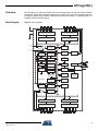
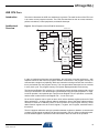
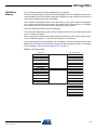
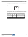
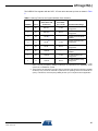
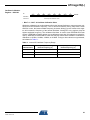
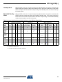
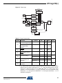
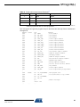
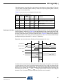
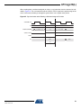
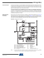
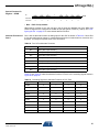
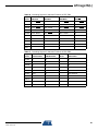
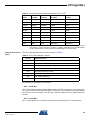
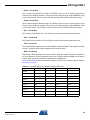
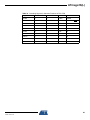
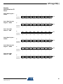
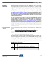
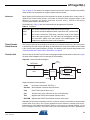
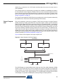
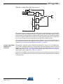
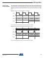
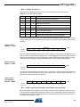
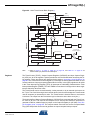
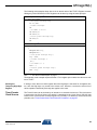
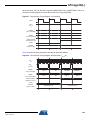
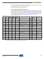
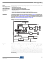
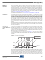
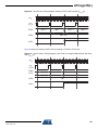
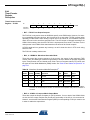
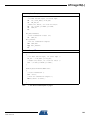
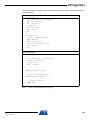
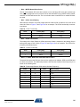
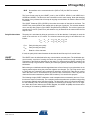
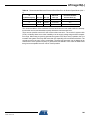
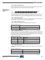
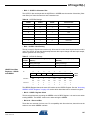
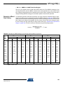
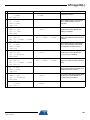
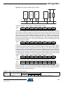
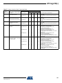
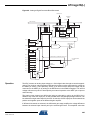
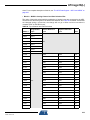
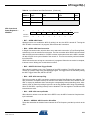
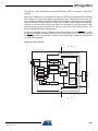
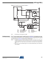
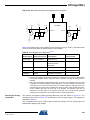
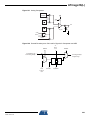
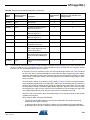
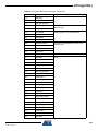
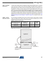
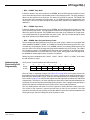
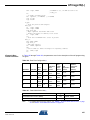
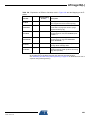
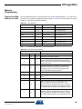
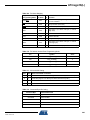
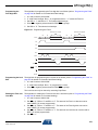
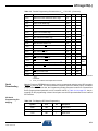
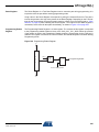
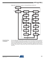
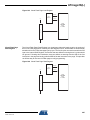
ATmega16(L)
Timer/Counter1
Control Register B –
TCCR1B
Bit
7
6
5
4
3
2
1
0
ICNC1
ICES1
–
WGM13
WGM12
CS12
CS11
CS10
Read/Write
R/W
R/W
R
R/W
R/W
R/W
R/W
R/W
Initial Value
0
0
0
0
0
0
0
0
TCCR1B
• Bit 7 – ICNC1: Input Capture Noise Canceler
Setting this bit (to one) activates the Input Capture Noise Canceler. When the Noise Canceler is
activated, the input from the Input Capture Pin (ICP1) is filtered. The filter function requires four
successive equal valued samples of the ICP1 pin for changing its output. The Input Capture is
therefore delayed by four Oscillator cycles when the Noise Canceler is enabled.
• Bit 6 – ICES1: Input Capture Edge Select
This bit selects which edge on the Input Capture Pin (ICP1) that is used to trigger a capture
event. When the ICES1 bit is written to zero, a falling (negative) edge is used as trigger, and
when the ICES1 bit is written to one, a rising (positive) edge will trigger the capture.
When a capture is triggered according to the ICES1 setting, the counter value is copied into the
Input Capture Register (ICR1). The event will also set the Input Capture Flag (ICF1), and this
can be used to cause an Input Capture Interrupt, if this interrupt is enabled.
When the ICR1 is used as TOP value (see description of the WGM13:0 bits located in the
TCCR1A and the TCCR1B Register), the ICP1 is disconnected and consequently the Input Capture function is disabled.
• Bit 5 – Reserved Bit
This bit is reserved for future use. For ensuring compatibility with future devices, this bit must be
written to zero when TCCR1B is written.
• Bit 4:3 – WGM13:2: Waveform Generation Mode
See TCCR1A Register description.
• Bit 2:0 – CS12:0: Clock Select
The three Clock Select bits select the clock source to be used by the Timer/Counter, see Figure
49 and Figure 50.
Table 48. Clock Select Bit Description
CS12
CS11
CS10
Description
0
0
0
No clock source (Timer/Counter stopped).
0
0
1
clkI/O/1 (No prescaling)
0
1
0
clkI/O/8 (From prescaler)
0
1
1
clkI/O/64 (From prescaler)
1
0
0
clkI/O/256 (From prescaler)
1
0
1
clkI/O/1024 (From prescaler)
1
1
0
External clock source on T1 pin. Clock on falling edge.
1
1
1
External clock source on T1 pin. Clock on rising edge.
113
2466T–AVR–07/10