Download Usage Restrictions - Renesas Electronics
Transcript
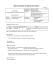
Microcontroller Technical Information
CP(K), O
IE-789468-NS-EM1
Emulation Board for Microcontrollers
μPD78932x, μPD78946x, μPD17932x
Document No.
ZBG-CD-06-0082
Date issued
September 27, 2006
Issued by
Development Tool Group
Multipurpose Microcomputer Systems Division
4th Systems Operations Unit
NEC Electronics Corporation
Usage Restrictions
Related
documents
IE-789468-NS-EM1 User’s
Manual: U16482EJ1V0UM00
Notification
classification
√
1/2
Usage restriction
Upgrade
Document modification
Other notification
1. Affected product
Product
IE-789468-NS-EM1
Outline
Emulation board for microcontrollers μPD78932x, μPD78946x,
Control CodeNote
A, B, C, D
μPD17932x
2. Restriction details
Restriction No. 7 has been added. See the attachment for details.
3. Workaround
See the attachment for details.
4. Modification schedule
Products in which No. 7 is modified are scheduled for release as follows.
Newly shipped products:
From the shipment of October 2006 (control codeNote: D)
Upgrade for already shipped products:
Available from October 10, 2006
* Note that this schedule is subject to change without notice. For the detailed release schedule of
modified products, contact an NEC Electronics sales representative.
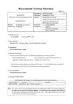
5. List of restrictions
See the attachment.
Note The “control code” is the second digit from the left in the 10-digit serial number staring with E.
If the product has been upgraded, a label indicating the new version is attached to the product and the
x in V-UP LEVEL x on this label indicates the control code.
ZBG-CD-06-0082
6. Document revision history
Document Number
Date Issued
Description
SBG-TT-0052-E
December 25, 2001
Addition of bug (No. 3)
SBG-TT-0122-E
June 5, 2002
Addition of bug (No. 4)
SBG-DT-04-0123
April 2, 2004
Classification of No. 2, No. 4, and No. 5 as restrictions
Addition of specification (No. 6)
ZBG-CD-06-0082
September 27, 2006
Addition of bug (No. 7)
2/2
ZBG-CD-06-0082
Attachment 1/4
Notes on Using IE-789468-NS-EM1
This document describes restrictions applicable only to the emulator and restrictions that are planned for
correction in the emulator.
Refer to the following documents for the restrictions in the target device.
• User’s manual of target device
• Restrictions notification document for target device
Also refer to the user’s manual of the emulator for cautions on using the emulator.
1. Product Version
Part number: IE-789468-NS-EM1
Control CodeNote
Remark
A
Emulation CPU μPD78F9328 V1.2
B
Emulation CPU μPD78F9328 V1.3
C
Emulation CPU μPD78F9328 V1.31/μPD78F9468 E1.3
D
Emulation CPU μPD78F9328 V1.31/μPD78F9468 E1.4
Note The “control code” is the second digit from the left in the 10-digit serial number staring with E.
If the product has been upgraded, a label indicating the new version is attached to the product and the
x in V-UP LEVEL x on this label indicates the control code.
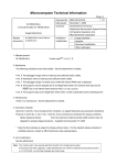
2. Product History
No.
1
2
Bugs and Changes/Additions to Specifications
Bug in port 4 operation
Control Code
A
B
C
D
×
√
√
√
Restriction on low-voltage emulation of μPD78932x or μPD17932x
Permanent restriction
microcontroller
3
Bug in LCD emulation of μPD78932x or μPD179327 microcontroller
4
Restrictions on LCD emulation of μPD78946x microcontroller
Permanent restriction
5
Restrictions on LCD emulation of μPD789327 or μPD179327
Permanent restriction
×
×
√
√
microcontroller
6
7
Addition of support for μPD17932x microcontrollers
Bug in low-voltage LCD emulation of μPD789327 or μPD179327
microcontroller
√
√
√
√
×
×
×
√
×: Applicable, √: Not applicable
ZBG-CD-06-0082
Attachment 2/4
3. Details of Bugs and Added Specifications
No. 1 Bug in port 4 operation
[Description]
A 1 V under-shoot waveform is generated during output.
When a value is input to port 4, the input value is not read correctly and 00h is read instead.
[Workaround]
This bug has been corrected in control code B and later.
No. 2 Restriction on low-voltage emulation of μPD78932x or μPD179327 microcontroller
[Description]
If 3-wire serial communication is performed at VDD = 1.8 to 2.5 V during emulation of a μPD789327x or
μPD17932x microcontroller, the SCK and SO signals are fixed at Hi level.
[Workaround]
Use the product with a voltage between 2.5 V and 5.5 V.
Regard this item as a permanent restriction.
No. 3 Bug in LCD emulation of μPD78932x or μPD17932x microcontroller
[Description]
The common and segment signals are not output with a normal waveform.
(1) The target device can output common and segment signals only by applying (connecting) a
voltage to the VLC0 pin. The IE-789468-NS-EM1 cannot output the common and segment
signals at the 1/3 VLCD and 2/3 VLCD levels. The initial status of the common signal is 3/3 VLCD =
VLC0, 1/3 VLCD, or 2/3 VLCD = GND, and that of the segment signal is low level.
(2) When the target device displays the LCD at 2.7 to 5.5 V, the LCD can be displayed with the
setting “no internal boost (VAON0 = 0)”. In the IE-789468-NS-EM1, however, the LCD cannot be
displayed unless the setting “internal boost enabled (VAON0 = 1)” is added to the program. By
enabling the internal boost (VAON0 = 1), the common and segment signals with 1/3 VLCD and
2/3 VLCD levels can be output.
(3) When a voltage less than 4.5 V is applied (connected) to the VLC0 pin, the 1/3 VLCD level is not
correctly output as common and segment signals. 1/3 VLCD = 1.5 V, 2/3 VLCD = 3.0 V
[Workaround]
There is no workaround.
This bug has been corrected in control code C and later.
No. 4 Restrictions on LCD emulation of μPD78946x microcontroller
[Description]
(1) If a voltage 4.5 V or higher is supplied to VDD when GAIN = 0, the LCD reference voltage becomes
0.5 to 1 V higher than the expected value.
(2) If a voltage 3.5 V or higher is supplied to VDD when GAIN = 1, the LCD reference voltage becomes
0.5 to 1 V higher than the expected value.
Remark GAIN = 0: 4.5 V specification LCD panel, GAIN = 1: 3 V specification LCD panel
ZBG-CD-06-0082
Attachment 3/4
[Workaround]
(1) When GAIN = 0, supply a voltage lower than 4.5 V to VDD.
(2) When GAIN = 1, supply a voltage lower than 3.5 V to VDD.
Regard these items as permanent restrictions.
No. 5 Restrictions on LCD emulation of μPD789327 or μPD179327 microcontroller
[Description]
(1) When VDD is VLC0 or higher (VDD ≥ VLC0), the LCD reference voltage becomes 0.5 to 1 V higher than
the expected value.
(2) The LCD function cannot be used if VDD is lower than 2 V (VDD < 2 V).
Remark VDD: Power supply voltage (1.8 to 5.5 V), VLC0: LCD driving voltage (1.8 to 5.5 V)
[Workaround]
(1) Emulate the LCD at VDD = VLC0.
(2) There is no workaround.
Regard these items as permanent restrictions.
No. 6 Addition of support for μPD17932x microcontrollers
[Description]
The μPD17932x microcontrollers are now supported.
The methods for emulation CPU selection and debugging are the same as those of the μPD78932x
microcontrollers.
No. 7 Bug in low-voltage LCD emulation of μPD789327 or μPD179327 microcontroller
[Description]
If VDD of 2 V or lower is applied while GAIN (reference voltage level selection bit) = 1 (1.0 V) and voltage
boost is enabled (VAON = 1) within approximately four seconds, the voltage is not boosted (VLC0 = 1 V,
VLC1 = 2 V, and VLC2 = 3 V are not set) but becomes VLC0 = VLC1 = VLC2 = 0 V. Consequently, the LCD
display may not be output.
[Workaround]
There is no workaround.
This bug has been corrected in control code D and later.
ZBG-CD-06-0082
Attachment 4/4
4. Cautions
(1) Read value of port 2 when the target system is not connected
Port 2 of the μPD78932x and μPD17932x microcontrollers is directly connected to a 1 MΩ pull-up
resistor. When the port value is read in input mode when the target system is not connected, the value
read from port 2 is 07h.
(2) Oscillation stabilization wait time cannot be changed
The oscillation stabilization wait time of the μPD78932x and μPD17932x microcontrollers (mask ROM
versions) after STOP mode is released by RESET input or power-on clear is the same as that of the
μPD78F9328 (flash memory version).
• Oscillation stabilization wait time: 215/fX (fixed)
(3) POC function of μPD78932x and μPD17932x microcontrollers
(a) When the IE-789468-NS-EM1 is started, bit 2 (POCOF1) of power-on-clear register 1 (POCF1)
becomes 1, which disables use of the power-on-clear function.
[Workaround] Clear bit 2 (POCOF1) to 0 in the startup routine.
(b) Even if a reset occurs due to power-on clear, the value of bit 2 (POCOF1) of power-on-clear register
1 (POCF1) does not change (POCOF1 remains 0).
[Workaround] There is no workaround.
(4) General cautions on handling this product
(a) Circumstances not covered by product guarantee
• If the product was disassembled, altered, or repaired by the customer
• If it was dropped, broken, or given another strong shock
• Use at overvoltage, use outside guaranteed temperature range, storing outside guaranteed
temperature range
• If power was turned on while the AC adapter, interface cable, or target system connection was in
an unsatisfactory state
• If the AC adapter cable, interface cable, target cable, or the like was bent or pulled excessively
• If an AC adapter other than the one supplied with the product is used
• If the product got wet
• If the product and target system were connected while a potential difference existed between the
GND of the product and the GND of the target system
• If a connector or cable was removed while the power was being supplied to the product
• If an excessive load was placed on a connector or socket
(b) Safety precautions
• If used for a long time, the product may become hot (50°C to 60°C).
Be careful of low
temperature burns and other dangers due to the product becoming hot.
• Be careful of electrical shock. There is a danger of electrical shock if the product is used as
described above in (a) Circumstances not covered by product guarantee.


