1
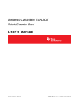
NCP5030MTTXGEVB
NCP5030 High Power
Lighting Evaluation Board
User's Manual
http://onsemi.com
EVAL BOARD USER’S MANUAL
Overview
OVP (Over−Voltage Protection). The high switching
frequency allows the use of a low value 4.7 mH inductor and
ceramic capacitors. The NCP5030 is in a low profile and
efficient thermally enhanced 3 x 4 mm DFN package.
The NCP5030 is a fixed frequency PWM buck−boost
converter optimized for constant current applications such
as driving high−powered white LED. The buck−boost is
implemented in an H−bridge topology and has an adaptive
architecture where it operates in one of three modes: boost,
buck−boost, or buck depending on the input and load
condition. This device has been designed with
high−efficiency for use in portable applications and is
capable of driving up to 1.2 A pulse current and 900 mA
continuous current into a high power LED for camera flash,
flashlight, torch and similar applications. To protect the
device cycle by cycle current limiting and a thermal
shutdown circuit have been incorporated as well as output
NCP5030 High Power Lighting Evaluation Board
This evaluation board demonstrates the overall NCP5030
capabilities and offers very easy current programming. The
output current is fully configurable via the usage of 4
external resistors and corresponding jumper headers. The
NCP5030 lighting evaluation board schematic is depicted in
Figure 2.
Figure 1. NCP5030MTTXGEVB Board Picture
© Semiconductor Components Industries, LLC, 2012
May, 2012 − Rev. 1
1
Publication Order Number:
EVBUM2111/D
NCP5030MTTXGEVB
SCHEMATIC
VLF5014 4R7/RLF7030 4R7
12
R108
82 k
1
CTRL
3
11
J102
CONN RECT 3
VOUT
AGND
COMP
FB
PGND
PCA
TP101
3 2 1
7
10
U101
R107
39 k
4 5 6
LX2
C105
10 m
VIN
C104
1m
2
1 13
VS
PVIN
R101
100 k
1
C101
330 p
J103
CONN RECT 2
LXCL−PWF1
C103
22 m
9
10 8 6 4 2
9 7 53 1
1
3 2 1
J105
J108
HEADER 6
1
2
3
4
5
6
Lambertian
2
1
200 mV
1
J111
ÇÇ
ÇÇ
ÇÇ
ÇÇ
ÇÇ
ÇÇ
ÇÇ
ÇÇ
ÇÇ
ÇÇ
ÇÇ
H1
J109
CONN RECT 5x2
H2
1
Fixed Hole
1
Fixed Hole
J107
3*AA Bat Holder
J101
HEADER 2
D102
2
TP102
C102
22 p
PVIN
2
D101
8
NCP5030 DFN
1
2
2
TP104
1
PVIN
LX1
LX1
1
1
R102 0.51
R103 0.51
R104 0.51
1
R105
2
R106
PVIN
J104
4.7 mH
L101
TP103
+ 1
−
2
J110
HEADER 2
1
GND
2
J106
CONN RECT 3
H3
1
Fixed Hole
H4
1
Fixed Hole
Figure 2. NCP5030 High Power Lighting Evaluation Board Schematic
Operation
CAUTION:
L101 selection depends on the output current,
VLF5014A4R7M1R1 is recommended at output current
under 500 mA, and RLF7030T4R7M3R4 is recommended
when output current is larger than 700 mA.
The power supply of NCP5030 should be from 2.7 V to
5.5 V. Maximum input voltage is 7.0 V and maximum
continuous output current is 900 mA.
1. Exceeding the maximum input voltage may
damage NCP5030 permanently!
2. Too long time duration at over output current
may decrease LED life time or even damage
LED!
Table 1. Input Power Connector
Symbol
Descriptions
J101−1
Positive terminal of external power supply
J101−2
GND of external power supply
J107−1
Positive terminal of 3*AA batteries in serial
J107−2
GND of 3*AA batteries in serial
Table 2. Output Power Connector
J108−1/2
VOUT of NCP5030
J108−5/6
FB of NCP5030
http://onsemi.com
2
NCP5030MTTXGEVB
Table 3. Jumper Setup
Symbol
Descriptions
J102−1/2
Peak current set to about 3 A, peak current and setting resistor selection can reference the datasheet of
NCP5030
J102−2/3
Peak current set to about 1.5 A, peak current and setting resistor selection can reference the datasheet of
NCP5030
J103
Short will connect CTRL to PVIN and enable NCP5030
J110
GND test jumper
J104
Must be connected to ensure NCP5030 work properly, can measure inductor current here, such as peak
current of inductor
J105
Select D101 as load of NCP5030, be careful if J111 or J108 is connected
J111
Select D102 as load of NCP5030, be careful if J105 or J108 is connected
J109
Output current setting, reference to table 5(Output current setting table)
Table 4. Test Points
TP101
CTRL and enable of NCP5030.
TP102
FB, feedback, reference voltage is 200 mV.
TP103
Switch LX1
TP104
Switch LX2
Current Setting Selection
The output is determined by the resistor or resistors
connected between FB pin and GND. R102 to R106 and
J109 are used for output current setting according to eq. 1:
Iout(A) + 0.2
R(W)
Where R is the total resistance between FB and GND,
J109 allows parallel connections of several resistors to select
output current.
Following is the output current setting table of J109
(1 = short connected; 0 = left open)
(eq. 1)
Table 5. Output Current Setting Table
PIN9−10
PIN7−8
PIN5−6
PIN3−4
PIN1−2
Output Current (mA)
0
0
0
0
1
100
0
0
0
1
0
200
0
0
0
1
1
300
0
0
1
0
0
400
0
0
1
0
1
500
0
0
1
1
0
600
0
0
1
1
1
700
0
1
1
0
0
800
0
1
1
0
1
900
http://onsemi.com
3
NCP5030MTTXGEVB
Efficiency Test
Figure 3 and Figure 4 describe efficiency results in different conditions.
Efficiency vs. VIN
100.0
350 mA
90.0
80.0
900 mA
500 mA
700 mA
70.0
60.0
50.0
40.0
30.0
20.0
10.0
5.50
5.40
5.30
5.20
5.10
5.00
4.90
4.80
4.70
4.60
4.50
4.40
4.30
4.20
4.10
4.00
3.90
3.80
3.70
3.60
3.50
3.40
3.30
3.20
3.10
3.00
2.90
2.80
2.70
2.60
0.0
Figure 3. Efficiency vs. Input Voltage, Rpca = 82 KW, load = LXHL − PW09,
Inductor = VLF5014A4R7M1R1 for Iout = 350 mA, 500 mA and 700 mA, RLF7030T4R7M3R4 for Iout = 900 mA
Efficiency vs. VIN
100.0
90.0
80.0
RLF7030T4R7M3R4
VLF5014A4R7M1R1
70.0
60.0
50.0
40.0
30.0
20.0
10.0
5.50
5.40
5.30
5.20
5.10
5.00
4.90
4.80
4.70
4.60
4.50
4.40
4.30
4.20
4.10
4.00
3.90
3.80
3.70
3.60
3.50
3.40
3.30
3.20
3.10
3.00
2.90
2.80
2.70
2.60
0.0
Figure 4. Efficiency vs. Input Voltage @ Inductor, Iout = 900 mA,
Rpca = 82 KW, load = LXHL − PW09, Vf = 3.9 V
http://onsemi.com
4
NCP5030MTTXGEVB
Output Current Regulation
Figure 5 shows the relationship between output current regulation Rpca and input voltage. There may be a tradeoff between
output current and input current limit.
Efficiency vs. VIN
1000.0
Rpca = 39 KW
900.0
800.0
Rpca = 82 KW
700.0
600.0
500.0
400.0
300.0
200.0
0.0
5.50
5.40
5.30
5.20
5.10
5.00
4.90
4.80
4.70
4.60
4.50
4.40
4.30
4.20
4.10
4.00
3.90
3.80
3.70
3.60
3.50
3.40
3.30
3.20
3.10
3.00
2.90
2.80
2.70
2.60
100.0
Figure 5. Output Current Regulation vs. Input Voltage @ Rpca, Iout = 900 mA
Inductor = RLF7030T4R7M3R4; Load = LXHL − PW09, Vf = 3.9 V
http://onsemi.com
5
NCP5030MTTXGEVB
PCB LAYOUT
Figure 6. Assembly Layer
Figure 7. Top Layer Routing
http://onsemi.com
6
NCP5030MTTXGEVB
BILL OF MATERIALS
ROHS
Compliant
1
Ceramic chip capacitor
330 pF
5%
0603
TDK
C1608C0G1H331J
Yes
Yes
C102
1
Ceramic chip capacitor
22 pF
5%
0603
TDK
C1608C0G1H220J
Yes
Yes
C103
1
Ceramic chip capacitor
22 mF
20%
0805
TDK
C2012X5R0J226M
Yes
Yes
C104
1
Ceramic chip capacitor
1 mF
20%
0603
TDK
C1608X5R0J105M
Yes
Yes
C105
1
Ceramic chip capacitor
10 mF
20%
0805
TDK
C2012X5R0J106M
Yes
Yes
L101
1
Chip winding magnetic
shielded inductor
4.7 mH
20%
4.5*4.7 mm
TDK
VLF5014AT-4R7M1R1
Yes
Yes
Qty
Description
Tolerance
C101
Designator
Substitution
Allowed
Table 6. BILL OF MATERIALS FOR THE NCP5030MTTXGEVB HIGH POWER LIGHTING EVALUATION BOARD
Value
Footprint
MFG
MFG Part
Number
6.8*7.3 mm
RLF7030T-4R7M3R4
R101
1
Chip resistor
100 KW
5%
0603
Std.
Std.
Yes
Yes
R102
1
Chip resistor
TBD (not
mounted)
NA
0805/1206
Std.
NA
NA
NA
R103,
R104
2
Chip resistor
0.51 W
1%,1/4W
0805/1206
Std.
Std.
Yes
Yes
R105
1
Chip resistor
1W
1%,1/8W
0805/1206
Std.
Std.
Yes
Yes
R106
1
Chip resistor
2.2 W
1%,1/8W
0805/1206
Std.
Std.
Yes
Yes
R107
1
Chip resistor
39 KW
5%
0603
Std.
Std.
Yes
Yes
R108
1
Chip resistor
82 KW
5%
0603
Std.
Std.
Yes
Yes
TP101TP104
4
PCB terminal 1 mm
NA
NA
Standard
1 mm
Std.
Std.
Yes
Yes
U101
1
Buck−Boost driver for
high power flash LED
NA
NA
WDFN12,
3*4 mm
NCP5030MTTXG
No
Yes
J101
1
Header X 2
NA
NA
SL5.08/2/90
J102,
J106
2
Header 3 pin, 0.1 inch
spacing
NA
NA
J103,
J104,
J105,
J111
4
Header 2 pin, 0.1 inch
spacing
NA
J107
1
3*AA Battery holder
J108
1
J109
ON Semiconductor
SL5.08/2/90B
Weidmüller
Yes
Yes
0.100*3
Std.
Std.
Yes
Yes
NA
0.100*2
Std.
Std.
Yes
Yes
NA
NA
1.84*2.25 mm
MPD
BH3AA−PC
No
Yes
Header 6
NA
NA
0.100*6
AMP
535676
No
Yes
1
Header 2*5,0.1 inch
spacing
NA
NA
0.100*2*5
Std.
Std.
Yes
Yes
J110
1
GND jumper
400 mil spacing
NA
NA
0.400
spacing
Yes
Yes
D101
1
LXCL−PWT1
NA
NA
2.0*1.6 mm
Lumileds
LXCL−PWT1
No
Yes
D102
1
Lambertian LED
modules
LUXEON I
LUXEON III
NA
Lambertian
Lumileds
LXHL−PW01
LXHL−PW09
Yes
Yes
http://onsemi.com
7
D3082−B01
Harwin
NCP5030MTTXGEVB
TEST PROCEDURE
18. Power off and configure J102 at 1−2 position;
19. Configure J109 in 100 mA position (pin1−2
shorted);
20. Power on, check D101 is lighting;
21. Power off, open J105, short J111 (if D102
mounted);
22. Power on, check D102 is lighting (if D102
mounted);
23. Power off, open J105, J111, connect J108 to
external LED or LED module (if there is);
24. Power on, check external LED or LED module is
lighting (if there is);
25. Power off;
26. Configure board default and connect jumpers
accordingly
• Place board in 300 mA output current
configuration:
• Place jumpers on J109 1−2(100 mA), 3−4(200
mA), 9−10(0 mA);
• Place a jumper on J102 2−3;
1. Visual inspection the board after solder, there
should be no short, redundant solder ball.
2. Measure the resistance of each pin of NCP5030 to
GND, there should be no short to GND (except pin
GND) or each other. Measure the forward and
backward resistance of D101/D102. Ensure solder
is good.
3. Short J104;
4. Short J103;
5. Short J106 2−3(power supply from J101);
6. Configure J102 in 2−3 position;
7. Short J105, open J111, J108;
8. Configure J109 in 100 mA position (pin1−2
shorted);
9. Configure power supply output voltage to 3.7 V.
10. Power off and connect power supply to J101;
11. Power on, check D101 is lighting;
12. Power off and Configure J109 in 200 mA position
(pin3−4 shorted);
13. Power on, check D101 is lighting;
14. Power off and Configure J109 in 400 mA position
(pin5−6 shorted);
15. Power on, check D101 is lighting;
16. Power off and Configure J109 in 400 mA position
(pin7−8 shorted);
17. Power on, check D101 is lighting;
• Place jumpers on J103/J104;
• Place a jumper on J105 and make sure J111 is
open;
• Place a jumper on J106 2−3;
ON Semiconductor and
are registered trademarks of Semiconductor Components Industries, LLC (SCILLC). SCILLC reserves the right to make changes without further notice
to any products herein. SCILLC makes no warranty, representation or guarantee regarding the suitability of its products for any particular purpose, nor does SCILLC assume any liability
arising out of the application or use of any product or circuit, and specifically disclaims any and all liability, including without limitation special, consequential or incidental damages.
“Typical” parameters which may be provided in SCILLC data sheets and/or specifications can and do vary in different applications and actual performance may vary over time. All
operating parameters, including “Typicals” must be validated for each customer application by customer’s technical experts. SCILLC does not convey any license under its patent rights
nor the rights of others. SCILLC products are not designed, intended, or authorized for use as components in systems intended for surgical implant into the body, or other applications
intended to support or sustain life, or for any other application in which the failure of the SCILLC product could create a situation where personal injury or death may occur. Should
Buyer purchase or use SCILLC products for any such unintended or unauthorized application, Buyer shall indemnify and hold SCILLC and its officers, employees, subsidiaries, affiliates,
and distributors harmless against all claims, costs, damages, and expenses, and reasonable attorney fees arising out of, directly or indirectly, any claim of personal injury or death
associated with such unintended or unauthorized use, even if such claim alleges that SCILLC was negligent regarding the design or manufacture of the part. SCILLC is an Equal
Opportunity/Affirmative Action Employer. This literature is subject to all applicable copyright laws and is not for resale in any manner.
PUBLICATION ORDERING INFORMATION
LITERATURE FULFILLMENT:
Literature Distribution Center for ON Semiconductor
P.O. Box 5163, Denver, Colorado 80217 USA
Phone: 303−675−2175 or 800−344−3860 Toll Free USA/Canada
Fax: 303−675−2176 or 800−344−3867 Toll Free USA/Canada
Email: [email protected]
N. American Technical Support: 800−282−9855 Toll Free
USA/Canada
Europe, Middle East and Africa Technical Support:
Phone: 421 33 790 2910
Japan Customer Focus Center
Phone: 81−3−5817−1050
http://onsemi.com
8
ON Semiconductor Website: www.onsemi.com
Order Literature: http://www.onsemi.com/orderlit
For additional information, please contact your local
Sales Representative
EVBUM2111/D