1
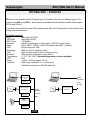
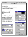
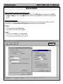
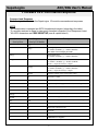
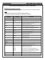
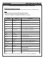
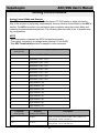
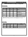
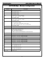
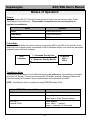
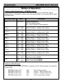
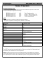
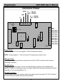
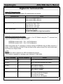
Model: ADC-x/DIG-x
RS-232 / RS-485
Data Acquisition
Digital I/O
v2.2 Firmware
Integrity Instruments
SuperLogics
SuperLogics
94 Falmouth Road
Newton, MA 02465 USA
Phone: (617) 332-3627
Fax: (617) 332-4687
Web: www.SuperLogics.com
1
SuperLogics
ADC/DIG User’s Manual
Table of Contents
Introduction
I/O Module features ..................................................................................
Quick Start - using Windows Hyperterminal ..............................................
3
4
Communications
RS-485 and RS-232 Packet Description ....................................................
6
Commands and Responses
Command & Response Table ....................................................................
Command & Response Examples RS-232 Interface ...................................
Command & Response Examples RS-485 Interface ...................................
Analog Control Nibble ..............................................................................
7
8
9
10
Module Configuration
DIP Switch and Jumpers ...........................................................................
EEPROM Map ..........................................................................................
11
12
Modes of Operation
Polled Mode ..............................................................................................
Timed/Async Mode ...................................................................................
Continuous Mode ......................................................................................
13
13
14
PCB Details
Board Illustration ......................................................................................
IC Description & LED Operation ..............................................................
17
17
Connector Pinouts
Digital & Analog Pinout ............................................................................
Power & Communications Pinout ..............................................................
RS-232 Cabling .........................................................................................
18
19
20
Digtial I/O Technical Info
Digital I/O Specifications and Control .......................................................
PWM ........................................................................................................
21
22
Analog Input Technical Info
Analog Specifications ................................................................................
Voltage References & Charge Pump Resistor ............................................
Analog Voltage Sampling & Conversion ...................................................
Analog Current Sampling & Conversion ....................................................
2
23
23
24
25
SuperLogics
ADC/DIG User’s Manual
Introduction - Features
Welcome to the wonderful world of SuperLogics I/O modules. We offer two different types of I/O
module lines: ADC-x and DIG-x. Each module is available with two different serial interface types:
RS-232 and RS-485.
All modules use exactly the same PCB populated with different ICs dependent on the interface and
Analog Input requirements.
I/O Module features:
MPU:
Microchip PIC16C65
EEPROM:
Microchip 25C040
MPU Clock:
7.3728 Mhz
Interface:
RS-485 (multidrop up to 255 nodes) or RS-232 (single ended)
Baud:
9600, 19200*, 57600, 115200 (DIP switch selectable, *=default)
LED:
Bicolor diagnostic LED
Watchdog:
MPU has built-in watchdog timer
POR:
MPU contains timed Power On Reset circuitry
Brownout:
MPU brownout detection ciruictry built-in
Temperature:
0°-70°C (32°-158°F) Extended temperature version available
PCB:
FR4
Power:
7.5Vdc - 30.0Vdc, approx. 50 ma.
Transient:
ZNR surge supression on +V power input
TransZorb protection on RS-485 data lines
485-25A
RS232-RS485
converter
RS-232
Full duplex
Host Controller
Address: 0
3 wire
50” max.
ADC-x
12 bit analog acquisition
16 bit digital I/O
Peripheral Module
Address: 1
ADC-x
12 bit analog acquisition
16 bit digital I/O
RS-485
multi-drop
1 pair wire
4000”+
DIG-x
16 bit digital I/O
Peripheral Module
Address: 2
Up to 255
modules!
3
SuperLogics
ADC/DIG User’s Manual
Quick Start
So, you’re in a hurry? Let’s see if we can help.
You need the following:
• HyperTerminal program (Windows 95/98 or Windows NT)
• An open COMPORT on your PC
• Power supply (we suggest a +9Vdc wall wart)
• A cable to connect your PC to your I/O Module (See PCB Details section for pinout)
• If you have an RS-485 interface, you need a 485-25E converter.
Make these DIP switch settings
SW1: OFF
SW2: ON RS-232 or OFF RS-485
SW3: ON
SW4: OFF
Step 2
Launch the HyperTerminal program
The HyperTerminal program is found under the
Programs - Accessories folder. Double click on the
Hypertrm.exe icon to launch the program.
HyperTerminal program configuration
1) Create a new connection named “Integrity”
2) Select your Comport (COM2 in the example)
3) Set COM Properties: 19200 baud, 8 data bits,
No parity, 1 stop bit, Flow control None
Step 3
Step 1
19200
4
SuperLogics
ADC/DIG User’s Manual
Quick Start
HyperTerminal program configuration cont.
4) Under the File menu, select Properties, click on the Settings tab, and adjust the ASCII
Setup settings for “Echo typed characters locally” and “Append line feeds to incoming line
ends”
Your First Command
Now that you have a HyperTerminal session running, you can start typing. After your first
command, see Commands and Responses section for more commands.
RS-232
• Type letter V and the Enter Key
• You should see V22 on the screen
RS485
• Type letters 0100V and the Enter Key
• You should see 0001V22 on the screen
Step 4
5
SuperLogics
ADC/DIG User’s Manual
Communications
The SuperLogics models ADC-x and DIG-x support both RS-232 and RS-485 communications
interfaces. Each interface type uses simple ASCII commands. A carriage return (decimal code
13 or Hex code 0x0D) marks the end of a data packet.
RS-232 Interface:
• RS-232 operates Full Duplex
• RS-232 modules can enter Continuous mode whereby the module is configured via
EEPROM settings to continuously communicate with the host computer to output its current
Digital, Counter or Analog readings.
RS-232 Command Format
Command/Response
ASCII
CR
carriage return
13 (0x0D hex)
RS-485 Interface:
• RS-485 operates Half Duplex
• Each module (node) on the bus has a unique Address 1 to 254 (0x01-0xFE hex)
• We use the latest Linear Technologies RS-485 bus drivers (LTC1487) allowing up to 255
nodes on the RS-485 multi-drop bus
• Address 0 (0x00 hex) is reserved for the Host controller
• Address 255 (0xFF hex) is reserved for Broadcast messages - accepted by all
modules on the RS-485 bus.
RS-485 Packet Format
Destination Address
xx
Source Address
xx
Command/Response
ASCII
x = ASCII Hexadecimal
Address 0x00
Address 0x01-0xFE
Address 0xFF
Host Device (IBM-PC, micro-controller, etc.)
I/O Module Address
Broadcast Address (used to configure an I/O Module)
6
CR
carriage return
13 (0x0D hex)
SuperLogics
ADC/DIG User’s Manual
Firmware v2.2 Command/Response
Command and Response
The following table illustrates the SuperLogics I/O module commands and responses.
NOTE
* All numeric data is represent as ASCII Hexadecimal integers (value x/y in the table)
* If a module receives an illegal or improperly formatted command, Error Response is sent.
* All ASCII characters are CASE SENSITIVE (use all capital letters!)
Command
Sent by Host
Response
Sent by I/O Module
Description
V
Vxy
Firmware version x.y
I
Ixxyy
Input digital port status
xx = PORT1 (PORTB) yy = PORT2 (PORTD)
Also returns current output port status
Oxxyy
O
Output digital port:
xx = PORT1 (PORTB) yy = PORT2 (PORTD)
Txxyy
T
Set digital direction:
xx = PORT1 (PORTB) yy = PORT2 (PORTD)
bit set(1) = Input, bit clear(0) = Output
G
Gxxyy
Get current digital direction:
xx = PORT1 (PORTB) yy = PORT2 (PORTD)
bit set(1) = Input, bit clear(0) = Output
N
Nxxxx
Get Pulse Counter (xxxx 16 bit counter value)
M
M
Clear Pulse Counter
Qy
Qyxxx
Bipolar sample analog (y control nibble , xxx analog value)
Uy
Uyxxx
Unipolar sample analog (y control niblle, xxx analog value)
K
Kxx
Get receive error count (xx current count)
J
J
Clear receive error count
Pxxyyy
P
PWM (xx = PWM frequency, yyy = PWM duty)
Wyyxx
W
Write EEPROM (yy address, xx value)
Ryy
Rxx
Read EEPROM (yy address in command, xx value in reponse)
S
S
Start stream continuous mode
H
H
Halt stream continuous mode
Z
Z
Reset CPU
X
Command error response
7
SuperLogics
ADC/DIG User’s Manual
Command/Response RS-232 Interface
RS-232 Interface Example Commands
The following table illustrates actual command and response data for an RS-232 interface.
NOTE
* All numeric data is represent as ASCII Hexadecimal integers
* The symbol ↵ equates to a carriage return (decimal 13, hex 0x0D)
Command
Sent by Host
Response
Sent by I/O Module
Description
V↵
V20↵
Module Firmware version 2.0
I↵
IFF00↵
Input digital port [PORT1 bits0-7 ON] [PORT2 bits0-7 OFF]
Note: this command also returns the current digital output
O007F↵
O↵
Output digital port [PORT1 bits 0-7 OFF]
[PORT2 bit 7 OFF, bits 0-6 ON]
TFF80↵
T↵
Set digital direction [PORT1 bits 0-7 INPUT]
[PORT2 bit 7 INPUT, bits 0-6 OUTPUT]
G↵
GFF80↵
Get current digital direction [PORT1 bits 0-7 INPUT]
[PORT2 bit 7 INPUT, bits 0-6 OUTPUT]
N↵
N0003↵
Get pulse counter: Current count = 3
M↵
M↵
Clear pusle counter: Current count = 0
Q1↵
Q100F↵
Bipolar analog control nibble = 0x1
Analog reading = 0x00F
U8↵
U840F↵
Unipolar analog control nibble = 0x8
Analog reading = 0x40F
K↵
K00↵
Current receive errors = 0
J↵
J↵
Clear receive error count: Current receive errors = 0
P08004↵
P↵
PWM freq = 51200 Hz, PWM duty = 12.5%
W0410↵
W↵
Write EEPROM Address 0x04 with value 0x10
R04↵
R10↵
Read EEPROM Adress 0x04 (value is 0x10)
S↵
S↵
IFF00↵
Q100F↵
IFF00↵
Q100F↵
...
START stream continuous mode
See Modes of Operation section
This example illustrates stream mode configured to
continuously update with Input Digital Port command and
Query Analog command with control 0x1. The module
continues until a command H↵ is received.
H↵
H↵
HALT stream continuous mode
Z↵
Z↵
Reset CPU (forces a watchdog timeout)
8
SuperLogics
ADC/DIG User’s Manual
Command/Response RS-485 Interface
RS-485 Interface Example Commands
The following table illustrates actual command and response data for an RS-485 interface.
NOTE
* All numeric data is represent as ASCII Hexadecimal integers
* Example Host Address = 0x00 and Module Address = 0x13
* The symbol ↵ equates to a carriage return (decimal 13, hex 0x0D)
Command
Sent by Host
Response
Sent by I/O Module
Description
1300V↵
0013V20↵
Module Firmware version 2.0
1300I↵
0013IFF00↵
Input digital port [PORT1 bits0-7 ON] [PORT2 bits0-7 OFF]
Note: this command also returns the current digital output
1300O007F↵
0013O↵
Output digital port [PORT1 bits 0-7 OFF]
[PORT2 bit 7 OFF, bits 0-6 ON]
1300TFF80↵
0013T↵
Set digital direction [PORT1 bits 0-7 INPUT]
[PORT2 bit 7 INPUT, bits 0-6 OUTPUT]
1300G↵
0013GFF80↵
Get current digital direction [PORT1 bits 0-7 INPUT]
[PORT2 bit 7 INPUT, bits 0-6 OUTPUT]
1300N↵
0013N0003↵
Get pulse counter: Current count = 3
1300M↵
0013M↵
Clear pulse counter: Current count = 0
1300Q1↵
0013Q100F↵
Bipolar analog control nibble = 0x1
Analog reading = 0x00F
1300U8↵
0013U840F↵
Unipolar analog control nibble = 0x8
Analog reading = 0x40F
1300K↵
0013K00↵
Current receive errors = 0
1300J↵
0013J↵
Clear receive error count: Current receive errors = 0
1300P08004↵
0013P↵
PWM freq = 51200 Hz, PWM duty = 12.5%
1300W0410↵
0013W↵
Write EEPROM Address 0x04 with value 0x10
1300R04↵
0013R10↵
Read EEPROM Adress 0x04 (value is 0x10)
1300S↵
0013X↵
START stream continuous mode
Illegal in RS-485 Mode
1300H↵
0013X↵
HALT stream continuous mode
Illegal in RS-485 Mode
1300Z↵
0013Z↵
Reset CPU (forces a watchdog timeout after Z↵ response sent
to Host)
NOTE: A command addressed to Module address 0xFF is accepted by all Modules
9
SuperLogics
ADC/DIG User’s Manual
Analog Control Nibble
Analog Control Nibble and Example
The ADC-x module utilizes the Linear Technologies LTC1296 analog to digital conversion
chip. In the process of performing a data sample, the user sends a control nibble to the ADC-x
module. The ADC-x module in turn performs a data conversion using the control nibble and
transmitts a response data sample back. The following table lists each of the 16 possible analog configurations.
NOTE
* All numeric data is represent as ASCII Hexadecimal integers
* The symbol ↵ equates to a carriage return (decimal 13, hex 0x0D)
* See ADC Technical Info section for sample to volts conversion
Control Nibble
Sent by Host
Analog Sample
0
Differential: CH0+ CH1-
1
Differential: CH2+ CH3-
2
Differential: CH4+ CH5-
3
Differential: CH6+ CH7-
4
Differential: CH0- CH1+
5
Differential: CH2- CH3+
6
Differential: CH4- CH5+
7
Differential: CH6- CH7+
8
Single-Ended: CH0
9
Single-Ended: CH2
A
Single-Ended: CH4
B
Single-Ended: CH6
C
Single-Ended: CH1
D
Single-Ended: CH3
E
Single-Ended: CH5
F
Single-Ended: CH7
Command
Sent by Host
Response
Sent by I/O Module
Description
Q0↵
Q100F↵
Bipolar (Q) sample differential CH0+ CH1- (Control = 0)
Analog sample = 0x00F (decimal 15)
UA↵
UA123↵
Unipolar (U) sample CH4 (Control = A )
Analog sample = 0x123 (decimal 291)
10
SuperLogics
ADC/DIG User’s Manual
Module DIP Switch & Jumper Configuration
DIP switch settings:
1
2
3
4
DIP switch position
OFF
OFF
9600 baud
ON
OFF
19200 baud
OFF
ON
57600 baud
ON
ON
115200 baud
ON
RS-232 packet
No packet addressing
OFF
RS-485 packet
Packet addressing used
ON
RS-485 Fast response
OFF
RS-485 Delayed response*
Wait approx. 2 ms. to send response
*NOTE: Use RS-485 delayed response when using the 485-25E protocol converter.
Jumper settings:
JP1
JP2
JP3
JP4
ON
ON
RS-485 active bus termination
OFF
OFF
No RS-485 bus termination
Not Used
Not Used
11
Jumper
SuperLogics
ADC/DIG User’s Manual
EEPROM Map - Module Configuration
Address
Description
0x00
Module Address (RS-485 address)
[factory default = 0x01]
0x01
Timed/Async Destination Address
[factory default = 0x00]
0x02
Data Direction Port 1 (PIC16C65 PORTB)
Bit set (1) = Input Bit clear (0) = Output
[factory default = 0xFF]
0x03
Data Direction Port 2 (PIC16C65 PORTD)
Bit set (1) = Input Bit clear (0) = Output
[factory default = 0xFF]
0x04
Timed/Async Update Configuration
0x00= No Timed/Async updates
0x01= Change Update on Digital Input or Counter change
0x02...0xFF = Timed Update (Time = Value * 100 milliseconds)
[factory default = 0x00]
0x05 ... 0x0E
Reserved
0x0F
Analog offset calibration (2’s complement integer offset to be added to analog bipolar sample)
0x10
Continuous Analog configuration count
0x00 = No analog stream readings
0x01..0x08 = Number of analog queries
See Modes of Operation Stream Continuous for locations 0x10...0x1A
0x11
Analog Query 1 - control byte - analog control nibble
0x12
Analog Query 2 - control byte - analog control nibble
0x13
Analog Query 3 - control byte - analog control nibble
0x14
Analog Query 4 - control byte - analog control nibble
0x15
Analog Query 5 - control byte - analog control nibble
0x16
Analog Query 6 - control byte - analog control nibble
0x17
Analog Query 7 - control byte - analog control nibble
0x18
Analog Query 8 - control byte - analog control nibble
0x19
Continuous Digital Input configuration
0x00 = Digital Input status OFF
0x01 = Digital Input status ON
0x1A
Continuous Pulse Counter configuration
0x00 = Pulse Counter status OFF
0x01 = Pulse Counter status ON
0x1B ... 0xFF
Available to User
12
SuperLogics
ADC/DIG User’s Manual
Modes of Operation
General
The SuperLogics RS-232 I/O modules can operate in three communications modes: Polled,
Timed/Async, and Continuous. These modes of operation can be used singularly or
together in combination.
Mode
Interface
Polled
RS-485 and RS-232
Timed/Async
RS-485 and RS-232
Continuous
RS-232
Polled Mode
By far, the Polled Mode is the most common usage of the ADC-x and DIG-x I/O modules. In this
mode the Host computer sends a command to the I/O Modules which in turn sends an associated
response back to the Host computer.
HOST
Computer
1 - Command Sent by Host
2 - Response Sent by Module
I/O Module
ADC-x
DIG-x
Timed/Async Mode
Timed/Async Mode refers to the I/O Module sending data without the Host sending a command
to poll the I/O Module. This can be viewed as the I/O Module sending a Response without the
Host first sending a Command. Async mode reduces communications bus traffic.
NOTE: Timed/Async mode is configured using EEPROM location 0x04.
Value at EEPROM Location 0x04
0x00
Timed/Async Mode disabled
0x01
Change Update
Digital Input or Pulse Counter change
0x02-0xFF
(decimal 2-255)
Timed Update
Time = Value * .1 second
Range = .2 second - 25.5 seconds
13
SuperLogics
ADC/DIG User’s Manual
Modes of Operation
Timed/Async Mode — Change Update
When EEPROM location 0x04 = 0x01, the ADC/DIG I/O module enters an asynchronous update
mode whereby any detected change on the Digital Input port or the Counter Capture port causes
the I/O module to transmit data to the host.
Status Change
Data Sent by I/O Module
Digital Input port change
Ixxxx
Counter Capture change
Nxxxx
HOST
Computer
1 - Data Sent by Module
I/O Module
ADC-x
DIG-x
Timer/Async Mode — Timed Update
When EEPROM location 0x04 = 0x02...0xFF, the ADC/DIG I/O module enters a timed update
mode whereby the I/O module will send data to the host after the specified time period has
elapsed.
Time Period = Value (EEPROM location 0x04) * .1 second
When using Async Timed Update, the I/O module uses the Continuous Mode configuration to
determine the data sent to the host.
Continuous Mode
The final mode of operation is Continuous mode. This mode constantly sends or streams data to
the host until the host halts the mode. Since the I/O module sends data continuously in this
mode, only the RS-232 interface can be configured for Continuous mode. (RS-485 is half
duplex and there would be no way to halt the stream of data coming from the I/O module!) In
brief, the I/O Module can send 0 thru 8 analog samples, digital input status, and the counter
capture status.
The I/O module uses parameters found in EEPROM locations 0x10 thru 0x1A to configure the
continuous mode. Therefore, the EEPROM must be configured before engaging the Continuous
mode.
Continuous mode setup steps
1 - Configure EEPROM locations 0x10 thru 0x1A
2 - Begin Continuous mode by sending command ‘S’ to the I/O Module
3 - Halt Continuous mode by sending command ‘H’ to the I/O Module
14
SuperLogics
ADC/DIG User’s Manual
Modes of Operation
Continuous Mode Configuration — EEPROM Locations
All parameters configuring the Stream Continuous mode are strored in EEPROM. See the
following table for a description of the locations and the parameters. Use command ‘W’ to update
EEPROM values.
EEPROM Location
Value
Description
0x10
0x00...0x08
Analog Configuration
0x00 = No analog samples
0x01...0x08 = Number of analog samples
0x11
0x0y ... 0x0y
0x8y ... 0x8y
Bipolar Analog: y = analog control nibble
Unipolar Analog: y = analog control nibble
0x0y ... 0x0y
0x8y ... 0x8y
Bipolar Analog: y = analog control nibble
Unipolar Analog: y = analog control nibble
0x0y ... 0x0y
0x8y ... 0x8y
Bipolar Analog: y = analog control nibble
Unipolar Analog: y = analog control nibble
0x0y ... 0x0y
0x8y ... 0x8y
Bipolar Analog: y = analog control nibble
Unipolar Analog: y = analog control nibble
0x0y ... 0x0y
0x8y ... 0x8y
Bipolar Analog: y = analog control nibble
Unipolar Analog: y = analog control nibble
0x0y ... 0x0y
0x8y ... 0x8y
Bipolar Analog: y = analog control nibble
Unipolar Analog: y = analog control nibble
0x0y ... 0x0y
0x8y ... 0x8y
Bipolar Analog: y = analog control nibble
Unipolar Analog: y = analog control nibble
0x0y ... 0x0y
0x8y ... 0x8y
Bipolar Analog: y = analog control nibble
Unipolar Analog: y = analog control nibble
0x19
0x00
0x01 ... 0xFF
Digital Input status disabled
Digital Input status enabled
0x1A
0x00
0x01 ... 0xFF
Pulse Counter status disabled
Pulse Counter status enabled
Sample 1
0x12
Sample 2
0x13
Sample 3
0x14
Sample 4
0x15
Sample 5
0x16
Sample 6
0x17
Sample 7
0x18
Sample 8
Continuous Mode Example
In this example, the I/O module EEPROM is configured to take 2 Analog samples and update the
Counter status.
EEPROM Location 0x10
EEPROM Location 0x11
EEPROM Location 0x12
EEPROM Location 0x1A
0x02
0x08
0x89
0x01
Take 2 Analog samples
Sample 1 - Bipolar sample CH0
Sample 2 - Unipolar sample CH2
Pulse Counter Status enabled
15
SuperLogics
ADC/DIG User’s Manual
Modes of Operation
Stream Mode Example cont.
The following table illustrates the Host Command and I/O Module responses for the stream
conrtinuous example configuration and usage.
EEPROM Location 0x10
EEPROM Location 0x11
EEPROM Location 0x12
EEPROM Location 0x1A
0x02
0x08
0x89
0x01
Take 2 Analog samples
Sample 1 - Bipolar sample CH0
Sample 2 - Unipolar sample CH1
Counter Status enabled
NOTE
* All numeric data is represent as ASCII Hexadecimal integers
* The symbol ↵ equates to a carriage return (decimal 13, hex 0x0D)
Host Sends
I/O Module Sends
W1002↵
W↵
W1108↵
W↵
W1289↵
W↵
W1A01↵
W↵
S↵
S↵
Continuous mode started
Q8023↵
U9823↵
N0044↵
Q8024↵
U9823↵
N0044↵
.... repeats continually
H↵
H↵
Continuous mode halted
The HOST may send any command during the Continuous mode and it will be accepted and
processed by the I/O Module as in normal operation.
NOTE: Engaging the Continuous mode at a high baud rate (115.2K baud) may overwhelm
certain Host computer systems due to the high volume of data transmitted on the RS-232 link.
The is especially true of slower 386 or 486 based systems running Windows 95 with limited
16
SuperLogics
ADC/DIG User’s Manual
PCB Details
Communications & Power
LED
U8
DIP switch
R18
JP2
U1
U6
JP1
JP3
JP4
U5
Digital I/O
U4
U3
U2
IC Description
U1
PIC16C65 MPU [44 pin PLCC]
U2* LTC1487 RS-485 driver [8 pin DIP]
U3* MAX202 RS-232 driver [16 pin DIP]
U4
25C040 EEPROM [8 pin DIP]
U5
LTC1296 [20 pin DIP]
U6
LM4040 Voltage Reference
U8
LMC555 Timer charge pump [8 pin DIP]
R18 Charge pump power supply resistor
NOTE*: U2 and U3 are mutually exclusive.
LED Operation
Blinking Green
Blinking Green
Blinking Red
No LED
Jumpers
JP1-JP2
JP3-JP4
[1 per Second]
[Rapid or Steady]
[Rapid or Steady]
Unit functioning correctly
Unit receiving serial data
Unit transmitting serial data
Unit is not functioning
Installed
Not used
RS-485 active termination at unit
17
Analog
Input
SuperLogics
ADC/DIG User’s Manual
1
2
3
4
5
6
7
8
9
10
11
12
13
Connector Pinout
14
15
16
17
18
19
20
21
22
23
24
25
DB25
Digital I/O Port
DB25 Digital Port pinout
DB25 Pin
Description
1
Port 2 bit 0 (PIC PORTD 0)
2
Port 2 bit 1 (PIC PORTD 1)
3
Port 2 bit 2 (PIC PORTD 2)
4
Port 2 bit 3 (PIC PORTD 3)
5
Port 2 bit 4 (PIC PORTD 4)
6
Port 2 bit 5 (PIC PORTD 5)
7
Port 2 bit 6 (PIC PORTD 6)
8
Port 2 bit 7 (PIC PORTD 7)
9
PWM output
10
N/A
11
+V_Unreg
12
+5Vdc
13
GND
14
Port 1 bit 0 (PIC PORTB 0)
15
Port 1 bit 1 (PIC PORTB 1)
16
Port 1 bit 2 (PIC PORTB 2)
17
Port 1 bit 3 (PIC PORTB 3)
18
Port 1 bit 4 (PIC PORTB 4)
19
Port 1 bit 5 (PIC PORTB 5)
20
Port 1 bit 6 (PIC PORTB 6)
21
Port 1 bit 7 (PIC PORTB 7)
22
Pulse Counter Input
23
-5Vdc
24
+5Vdc
25
GND
18
SuperLogics
ADC/DIG User’s Manual
Connector Pinout
shield
B —— RS-485
RxD — RS-232
GND
A —— RS-485
TxD — RS-232
+V
LED
U8
Communications & Power
GND
DIP switch
CH7 (CH3-)
CH6 (CH3+)
JP2
U1
CH5 (CH2-)
JP3
JP1
CH4 (CH2+)
JP4
CH3 (CH1-)
U5
CH2 (CH1+)
CH1 (CH0-)
Digital I/O
U4
CH0 (CH0+)
U3
U2
Analog
Input
Power Supply
7.5-30Vdc approx. 50 ma. (we suggest a 12Vdc 250ma power supply)
NOTE: Voltage supplies > 17Vdc must alter R18 charge pump resistor value.
GND and Shield
The GND and Shield terminals are connected on the ADC-x/DIG-x board and are therefore
electrically equivalent.
RS-485 Cabling
RS-485 wiring is quite simple. Connect all node A signals together and all node B signals
together. Simply run a twisted pair wire to all nodes. Please note that some systems may denote
signal A as T+/R+ and signal B as T-/R-.
RS-485 Termination
The two nodes (units) at the extreme ends of the cable must be terminated: JP1 & JP2 installed.
Ensure that only two nodes maximum are terminated.
19
SuperLogics
ADC/DIG User’s Manual
Connector Pinout
LED
8
9
5 - SHD
4
3 - TxD
2 - RxD
1
DB9
13
12
11
10
9
8
7 - GND
6
5
4
3 - RxD
2 - TxD
1
DB25
7
6
25
24
23
22
21
20
19
18
17
16
15
14
RS-232 Cabling
The RS-232 interface uses a “3 wire” RS-232 connection. That is to say only three wires are
connected between the I/O Module and the Host PC: TxD, RxD and SHD.
LED
Communications & Power
Communications & Power
DIP switch
DIP switch
RS-232 Hardware Flow Control
Some RS-232 interfaces may require certain control signals to be wired loopback in order to
support various Hardware Flow control schemes.
If your Host PC or Controller is using Hardware Flow control for serial communications, then use
the following chart to loopback the control signals.
RTS-CTS
DSR-DTR-CD
DB25: pins 5-4 wired together
DB25: pins 20-8-6 wired together
DB9: pins 8-7 wired together
DB9: pins 6-4-1 wired together
RS-232 Software Flow Control - Xon/Xoff
The SuperLogics ADC-x/DIG-x I/O modules do not support Xon/Xoff flow control.
20
SuperLogics
ADC/DIG User’s Manual
Digital I/O Technical Info
Digital I/O Characteristics
The following chart lists the Digital I/O characteristics and values.
Characteristic
Value
Digital I/O Current
I/O line source & sink 25 ma
Total current PORT1 200 ma
Total current PORT2 200 ma
Digital I/O Voltage Levels
Input Off (0) = 0V - 0.8V
Input On (1) = 2.0V - 5.0V
Output Off (0) = 0.6V max.
Output On (1) = 4.3V min.
Pulse Counter Input
1 Mhz max. input rate
16 bit counter capture
Counter increments on high-low transition
Digital Port Configuration Example
Any Digital I/O configuration changes made to the I/O Module using the ‘T’ command are
stored in EEPROM locations 0x02 and 0x03.
EEPROM Location 0x02
EEPROM Location 0x03
Port 1 I/O Configuration
Port 2 I/O Configuration
When using either the ‘T’ command or directly writing to EEPROM using the ‘W’ command, a
binary 1 at a bit location puts the I/O line into Input mode, while a binary 0 at a bit location puts
the I/O line into Output mode.
NOTE
* All numeric data is represent as ASCII Hexadecimal integers
* The symbol ↵ equates to a carriage return (decimal 13, hex 0x0D)
Host Command
Module Response
Action
T0000↵
T↵
All I/O lines are configured as Outputs
TFFFF↵
T↵
All I/O lines are configured as Inputs
TFF00↵
T↵
Port 1 bits 0-7 Inputs
Port 2 bits 0-7 Outputs
T00FF↵
T↵
Port 1 bits 0-7 Outputs
Port 2 bits 0-7 inputs
T1234↵
T↵
Port 1 bits 4,1 Inputs
Port 1 bits 7,6,5,3,2,0 Outputs
Port 2 bits 4,5,2 Inputs
Port 2 bits 7,6,3,1,0 Outputs
21
SuperLogics
ADC/DIG User’s Manual
Digital I/O Technical Info
Pulse Width Modulation (PWM)
The ADC-x and DIG-x I/O modules have a configurable PWM output. There are two settings to
configure for proper PWM operation: PWM frequency and PWM duty cycle. The current
capability of the PWM output is the same as a Digital I/O line (source & sink 25 ma.)
PWM — Command
Pxxyyy
xx = Pwm_Divisor
yyy = Pwm_Duty (10 bits max.)
Pwm_Divisor = 0x00 ... 0xFF
Pwm_Duty = 0x000 ... 0x3FF
Pwm_Duty = 0, PWM output is disabled (output 0)
PWM — Control
Fpwm = Frequency of PWM output in Hz
Pwm_Duty_Percentage = PWM duty cycle (output % on for period Fpwm)
Fpwm = 460800 Hz / (Pwm_Divisor + 1)
Duty_Resolution = log (1843200/Fpwm) / log (2)
Duty_Resolution
Pwm_Duty_Percentage = Pwm_Duty / 2
Pwm_Divisor
Fpwm
Duty_Resolution
0xFF
(255)
1800 Hz
10 bits*
0xFE
(254)
1807 Hz
10 bits
0x08
(8)
51200 Hz
5 bits
0x00
(0)
460800 Hz
2 bits
If (Pwm_Duty > Duty_Resolution), then
Pwm_Duty_Percentage = 100%
*Note: Pwm_Divisor 0xFF cannot
achieve complete 100% duty cycle. Use
Pwm_Divisor 0xFE if 100% duty cycle
is required.
Example PWM Commands
* All numeric data is represent as ASCII Hexadecimal integers
* The symbol ↵ equates to a carriage return (decimal 13, hex 0x0D)
Host Command
Module Response
Action
P0000↵
P↵
PWM off
Any duty cycle of 0 disables PWM output
P08004↵
P↵
PWM frequency = 51200 Hz
PWM duty = 12.5%
PFE3FF↵
P↵
PWM frequency = 1807 Hz
PWM duty = 100%
PFE200↵
P↵
PWM frequency = 1807 Hz
PWM duty = 50%
22
SuperLogics
ADC/DIG User’s Manual
Analog Input Technical Info
Analog Characteristics
Characteristic
Value
A/D Converter
Linear Tech LTC1296BCN ± .5 LSB
Linear Tech LTC1296DCN ± 2 LSB
Linearity Error
Models: ADC-1/-2/-5/-6 LTC1296BCN ± 0.012% (± .5 LSB)
Models: ADC-3/-4/-7/-8 LTC1296DCN ± 0.018% (± .75 LSB)
Gain Error
Models: ADC-1/-2/-5/-6 ± 0.012% (± .5 LSB)
Models: ADC-3/-4/-7/-8 ± 0.39% (± 4 LSB)
Offset Error
Models: ADC-1/-2/-5/-6 ± 0.17%
Models: ADC-3/-4/-7/-8 ± 1.17%
Temperature Drift
100 ppm/ºC ( max. )
Max Input Voltage
70V over-voltage protected (R17 10K DIP)
15V over-voltage protected (R17 1K DIP)
Bandwidth
> 1500 SPS max. in continuous mode
Voltage References
We utilize two distinct voltage references in the ADC-x Module: a 0.1% voltage reference and
a 1.0% voltage reference. These voltage references may be changed by the user. We have
included Digikey part numbers for easy ordering. (Digikey phone: 1-800-344-4539)
Voltage
Digikey Part Number
5.000V
voltage range +5.0Vdc to -5.0Vdc
0.1% LM4040AIZ-5.0-ND
1.0% LM4040DIZ-5.0-ND
4.096V
voltage range +4.1Vdc to -4.1Vdc
0.1% LM4040AIZ-4.1-ND
1.0% LM4040DIZ-4.1-ND
2.500V
voltage range +2.5Vdc to -2.5Vdc
0.1% LM4040AIZ-2.5-ND
1.0% LM4040DIZ-2.5-ND
1.200V
voltage range +1.2Vdc to -1.2Vdc
0.5% LM4041CIZ-1.2-ND
Charge Pump Resistor
The ADC-x module contains a negative voltage supply in the form of a charge pump driven by
U8, an LMC555 timer. This charge pump obtains its voltage from the unregulated power supply
input. Since the LMC555 is rated only for +15Vdc, we have designed a simple zener diode
power supply fed through R18 to regulate the power into the LMC555 to +12Vdc.
If the power supply voltage > 17Vdc, R18 needs to be replaced with a 1.2K resistor.
23
SuperLogics
ADC/DIG User’s Manual
Analog Input Technical Info
Charge Pump Resistor cont.
We supply a 1.2K 1/2W resistor with each ADC-x module.
Power supply Voltage
R18 Value
7.5Vdc to 17.0Vdc
120 ohm 1/4W (factory default)
17.1Vdc to 30Vdc
1.2K ohm 1/2W (supplied - not installed)
Sampling Analog Voltage Inputs
By far the most common configuration of the ADC-x is to sample voltage values. Analog
voltage levels are converted to integer digital values using the Linear Technologies LTC1296
A/D (Analog/Digital) chip. The input voltage range is determined by the reference voltage.
There are two analog sample types: Unipolar and Bipolar
Both A/D sampling types result in a 12 bit binary integer value. This binary integer value is
converterd to a voltage depending on the sample type.
Unipolar Analog Sampling
Unipolar analog sampling span is from ground (GND) to voltage reference (Vref). Only positive
voltages are sampled in unipolar mode. The unipolar sample is represented as an unsigned
integer as follows:
Unipolar voltages: 0V ... +Vref
The benefit of using Unipolar samples over Bipolar samples is that a 12bit binary value is
spread out over less total voltage span (Vref total.)
1bit unipolar = Vref/4096
Bipolar Analog Sampling
Bipolar analog sampling span is from -Vref to +Vref. Both negative and positive voltages are
sampled and represented as a signed binary integer (2’s complement) as follows:
Bipolar voltages:
-Vref ... 0 ... +Vref
The benefit of using Bipolar sampling over Unipolar is obvious, negative voltages! The downfall
of using Bipolar sampling is that a 12 bit binary value is spread out over a larger total voltage
span (2*Vref total.)
1bit bipolar = Vref/2048
24
SuperLogics
ADC/DIG User’s Manual
Analog Input Technical Info
Voltage Conversion
The Analog conversion value obtained from the ADC-x module is represented as an integer
value (either signed for Bipolar samples or unsigned for Unipolar sample) and is normally
converted to a Real or Floating Point number for ultimate usage.
Vref = 5.000, 4.096, 2.500 or 1.200V
Unipolar Conversion, ADC_Sample is an unsigned integer value
Volts [unipolar] = ADC_Sample * (Vref/4096)
Bipolar Conversion, If ADC_Sample is a signed integer value
If you are fortunate enough to convert the Bipolar ASCII hexadecimal value directly to a signed
integer, then conversion from ADC_Sample to volts is very simple.
Volts [bipolar] = ADC_Sample * (Vref/2048) + Offset_Calibration
Bipolar Conversion, If ADC_Sample is an unsigned integer value
Most often the ADC_Sample value is represented as an unsigned integer, quite common
when converting the Bipolar ASCII hexadecimal analog reading using the ‘C’ language scanf()
function. If an unsigned integer is used, we must manually calculate a negative number.
if (ADC_Sample >= 2048)
Volts [bipolar] = (ADC_Sample-4097) * (Vref/2048) + Offset_Calibration
if (ADC_Sample <= 2047)
Volts [bipolar] = ADC_Sample * (Vref/2048) + Offset_Calibration
Offset Calibration
The Linear Technologies LTC1296 A/D converter used in the ADC-x modules can exhibit an
offset phenomenon. This offset phenomenon is unique to each LTC1296 and a calibration of
the offset is required to obtain the most accurate analog readings. The offset calibration is used
only with Bipolar analog samples.
To obtain the current A/D offset use the following procedure:
1 - Connect analog CH0 to GND (use a jumper or clip lead)
2 - Take a Bipolar analog reading
3 - The negative (opposite sign) of this value is the offset calibration to be added to samples
At the factory an offset calibration is performed and stored in EEPROM location 0x0F as an 8
bit 2’s complement number.
Offset_Stored = 8 bit value at EEPROM location 0x0F
if (Offset_Stored >= 128)
Offset_Calibration = (Offset_Stored - 256) * (Vref/2048)
if (Offset_Stored <= 127)
25
SuperLogics
ADC/DIG User’s Manual
Analog Input Technical Info
Sampling Current (4-20 ma) Inputs
Many devices output a current value instead of a voltage value. The secret to obtaining current
readings is a 250 ohm resistor and a 5V voltage reference. Placing a 250 ohm resistor to
ground on a 4-20 ma. current input will create a voltage potential of 1V to 5V.
If we remember Ohm’s law:
4-20 ma current input
CHx analog input channel
E=I*R
250 ohm
R = 250 ohms
I = .004 to .020 amps (4-20 ma.)
E = 1.0V to 5.0V
NOTE: We supply several ultra precision 250 ohm 0.1% resistors with each ADC-x module.
Obtaining current readings is a three step process:
1 - Perform analog Unipolar sample (5.000V reference must be used!)
2 - Convert unipolar sample to volts
3 - Convert voltage to amps
Current Conversion
The following formula will convert the raw analog sample reading to a current value.
Current = ADC_Sample * (5.000/4096) * 250
Obtaining accurate Analog samples
Please keep the following points in mind when attempting to obtain accurate samples.
A) Watch out for UPS systems! They create loads of EMI/EMF noise.
B) Keep the analog signal source as close to the ADC-x module as possible.
C) Keep transformers far away from the ADC-x module.
D) Avoid high impedance analog signal sources.
E) Use good wiring practices, especially in regards to ground connections.
F) RS-232 interface can generate approx. 2 mv noise.
G) RS-485 interface offers the best noise immunity.
Warranty
SuperLogics warranties all products against defective workmanship and components for a period
of one year after purchase. SuperLogics agrees to repair or replace, at its sole discretion, a
defective product if returned to SuperLogics with proof of purchase within this period.
26