1
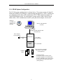
To our customers, Old Company Name in Catalogs and Other Documents On April 1st, 2010, NEC Electronics Corporation merged with Renesas Technology Corporation, and Renesas Electronics Corporation took over all the business of both companies. Therefore, although the old company name remains in this document, it is a valid Renesas Electronics document. We appreciate your understanding. Renesas Electronics website: http://www.renesas.com April 1st, 2010 Renesas Electronics Corporation Issued by: Renesas Electronics Corporation (http://www.renesas.com) Send any inquiries to http://www.renesas.com/inquiry. Notice 1. 2. 3. 4. 5. 6. 7. All information included in this document is current as of the date this document is issued. Such information, however, is subject to change without any prior notice. Before purchasing or using any Renesas Electronics products listed herein, please confirm the latest product information with a Renesas Electronics sales office. Also, please pay regular and careful attention to additional and different information to be disclosed by Renesas Electronics such as that disclosed through our website. Renesas Electronics does not assume any liability for infringement of patents, copyrights, or other intellectual property rights of third parties by or arising from the use of Renesas Electronics products or technical information described in this document. No license, express, implied or otherwise, is granted hereby under any patents, copyrights or other intellectual property rights of Renesas Electronics or others. You should not alter, modify, copy, or otherwise misappropriate any Renesas Electronics product, whether in whole or in part. Descriptions of circuits, software and other related information in this document are provided only to illustrate the operation of semiconductor products and application examples. You are fully responsible for the incorporation of these circuits, software, and information in the design of your equipment. Renesas Electronics assumes no responsibility for any losses incurred by you or third parties arising from the use of these circuits, software, or information. When exporting the products or technology described in this document, you should comply with the applicable export control laws and regulations and follow the procedures required by such laws and regulations. You should not use Renesas Electronics products or the technology described in this document for any purpose relating to military applications or use by the military, including but not limited to the development of weapons of mass destruction. Renesas Electronics products and technology may not be used for or incorporated into any products or systems whose manufacture, use, or sale is prohibited under any applicable domestic or foreign laws or regulations. Renesas Electronics has used reasonable care in preparing the information included in this document, but Renesas Electronics does not warrant that such information is error free. Renesas Electronics assumes no liability whatsoever for any damages incurred by you resulting from errors in or omissions from the information included herein. Renesas Electronics products are classified according to the following three quality grades: “Standard”, “High Quality”, and “Specific”. The recommended applications for each Renesas Electronics product depends on the product’s quality grade, as indicated below. You must check the quality grade of each Renesas Electronics product before using it in a particular application. You may not use any Renesas Electronics product for any application categorized as “Specific” without the prior written consent of Renesas Electronics. Further, you may not use any Renesas Electronics product for any application for which it is not intended without the prior written consent of Renesas Electronics. Renesas Electronics shall not be in any way liable for any damages or losses incurred by you or third parties arising from the use of any Renesas Electronics product for an application categorized as “Specific” or for which the product is not intended where you have failed to obtain the prior written consent of Renesas Electronics. The quality grade of each Renesas Electronics product is “Standard” unless otherwise expressly specified in a Renesas Electronics data sheets or data books, etc. “Standard”: 8. 9. 10. 11. 12. Computers; office equipment; communications equipment; test and measurement equipment; audio and visual equipment; home electronic appliances; machine tools; personal electronic equipment; and industrial robots. “High Quality”: Transportation equipment (automobiles, trains, ships, etc.); traffic control systems; anti-disaster systems; anticrime systems; safety equipment; and medical equipment not specifically designed for life support. “Specific”: Aircraft; aerospace equipment; submersible repeaters; nuclear reactor control systems; medical equipment or systems for life support (e.g. artificial life support devices or systems), surgical implantations, or healthcare intervention (e.g. excision, etc.), and any other applications or purposes that pose a direct threat to human life. You should use the Renesas Electronics products described in this document within the range specified by Renesas Electronics, especially with respect to the maximum rating, operating supply voltage range, movement power voltage range, heat radiation characteristics, installation and other product characteristics. Renesas Electronics shall have no liability for malfunctions or damages arising out of the use of Renesas Electronics products beyond such specified ranges. Although Renesas Electronics endeavors to improve the quality and reliability of its products, semiconductor products have specific characteristics such as the occurrence of failure at a certain rate and malfunctions under certain use conditions. Further, Renesas Electronics products are not subject to radiation resistance design. Please be sure to implement safety measures to guard them against the possibility of physical injury, and injury or damage caused by fire in the event of the failure of a Renesas Electronics product, such as safety design for hardware and software including but not limited to redundancy, fire control and malfunction prevention, appropriate treatment for aging degradation or any other appropriate measures. Because the evaluation of microcomputer software alone is very difficult, please evaluate the safety of the final products or system manufactured by you. Please contact a Renesas Electronics sales office for details as to environmental matters such as the environmental compatibility of each Renesas Electronics product. Please use Renesas Electronics products in compliance with all applicable laws and regulations that regulate the inclusion or use of controlled substances, including without limitation, the EU RoHS Directive. Renesas Electronics assumes no liability for damages or losses occurring as a result of your noncompliance with applicable laws and regulations. This document may not be reproduced or duplicated, in any form, in whole or in part, without prior written consent of Renesas Electronics. Please contact a Renesas Electronics sales office if you have any questions regarding the information contained in this document or Renesas Electronics products, or if you have any other inquiries. (Note 1) “Renesas Electronics” as used in this document means Renesas Electronics Corporation and also includes its majorityowned subsidiaries. (Note 2) “Renesas Electronics product(s)” means any product developed or manufactured by or for Renesas Electronics. User’s Manual LCE-780308-EM Emulation Board Preliminary Document No. U18142EU1V0UM00 (1st edition) Preliminary Version 10/26/01 2001 NEC Electronics Inc. All rights reserved. Printed in U.S.A. LCE-780308-EM User’s Manual No part of this document may be copied or reproduced in any form or by any means without the prior written consent of NEC Electronics Inc. (NECEL). The information in this document is subject to change without notice. All devices sold by NECEL are covered by the provisions appearing in NECEL's Terms and Conditions of Sales only, including the limitation of liability, warranty, and patent provisions. NECEL makes no warranty, express, statutory, implied or by description, regarding information set forth herein or regarding the freedom of the described devices from patent infringement. NECEL assumes no responsibility for any errors that may appear in this document. NECEL makes no commitments to update or to keep current information contained in this document. The devices listed in this document are not suitable for use in applications such as, but not limited to, aircraft control systems, aerospace equipment, submarine cables, nuclear reactor control systems and life support systems. “Standard” quality grade devices are recommended for computers, office equipment, communication equipment, test and measurement equipment, machine tools, industrial robots, audio and visual equipment, and other consumer products. For automotive and transportation equipment, traffic control systems, anti-disaster and anti-crime systems, it is recommended that the customer contact the responsible NECEL salesperson to determine the reliability requirements for any such application and any cost adder. NECEL does not recommend or approve use of any of its products in life support devices or systems or in any application where failure could result in injury or death. If customers wish to use NECEL devices in applications not intended by NECEL, customers must contact the responsible NECEL salespeople to determine NECEL's willingness to support a given application. 2 LCE-780308-EM User’s Manual CHAPTER 1 GENERAL INFORMAT ION The LCE-780308-EM is an emulation board or daughter board for the LCE-K0 development system, supporting NEC’s uPD780058, uPD78054, uPD78064, and uPD780308 sub-series of 8-bit single-chip microcontrollers. By combining this daughter board with the LCE-78K0 motherboard, these sub-series can be emulated efficiently. The LCE-780308-EM is shipped with the following contents: • • • • LCE-780308-EM daughter board User’s manual Two 50-pin ribbon cables CD-ROM containing debugger, assembler, compiler, device files, and documentation. 1.1. Basic Configuration Parameter Subseries Supported uPD780058 subseries Description Target Devices uPD780053GC, uPD780053GK, uPD780054GC, uPD780054GK, uPD780055GC, uPD780055GK, uPD780056GC, uPD780056GK, uPD780058GC, uPD780058GK uPD78052GC, uPD78052GK, uPD78053GC, uPD78053GK, uPD78054GC, uPD78054GK, uPD78055GC, uPD78055GK, uPD78056GC, uPD78056GK, uPD78058GC, uPD78058GK uPD78054 subseries uPD78064 subseries uPD78062GC, uPD78062GF, uPD78063GC, uPD78063GF, uPD78064GC, uPD78064GF uPD780308 subseries uPD780306GC, uPD780306GF, uPD780308GC, uPD780308GF Clock supply Internal: Installed on the motherboard External: Pulse input At least 2V Low-voltage compatible 3 LCE-780308-EM User’s Manual 1.2. LCE-K0 System Configuration The LCE-K0 system configuration is as shown below. The system consists of a host PC, running the ID78K0-LCE debugger, communicating through the PC’s LPT1: parallel port via a standard parallel cable, to the combination of LCE-78K0 motherboard plus LCE780308-EM daughter board. For connection to a target system, either a pair of 50-pin ribbon cables, or the combination of an NEC probe plus socket adapter, can be used. Debugger ID-78K0-LCE & Device File DF78K0 Host PC with Windows 95/98/NT Straight-Through Parallel Cable (sold separately) Power adapter (sold separately) Motherboard Daughter Board LCE-78K0 (sold separately) LCE-780308-EM Probe: NP-80GC NP-80GK, NP-100GC or NP-100GF (sold separately) 2 Ribbon cables Conversion Socket EV-9200GC-80 for NP-80GC probe; EV-TGK-080SBW for NP-80GK probe; EV-TGC-100SDW for NP-100GC probe; EV-9200GF-100 for NP-100GF probe; (sold separately) 4 LCE-780308-EM User’s Manual CHAPTER 2 COMPONENTS This chapter introduces the main components of the LCE-780308-EM daughter board unit. 2.1. Daughter Board Layout Figure 2.1-1 LCE-780308 Top Layout 5 LCE-780308-EM User’s Manual This is a drawing of the top of the LCE-780308-EM board; this side will face upward in the assembled system. U1 is a uPD78P0308 device, and U2 is a uPD78P054 device. Together these two devices provide emulation of the peripheral devices such as parallel ports, serial ports, timers, LCD drivers, etc., for the supported 78K0 devices. J1, J2, J3, J4, and J5 are connectors to the user target system. These connectors contain all the pins available on the emulated device. J1 and J2 are KEL connectors for device probes, while J3, J4 and J5 are dual-row male shrouded headers with latching levers for the ribbon cables. Please see the section below about ribbon cables and probes, and Chapter 4 for pin assignments of these connectors. D7 is an LED which is used to indicate that power is applied to the target system. JP1, JP2, JP3, and JP6 are jumpers for analog voltages. They allow the optional connection of analog signals AVDD, AVREF0, AVREF1, and AVSS to power, ground or reference voltages provided on the LCE-780308-EM board, when these analog voltages are not provided in the user target system. JP4 is provided for optional on-board connection of LCD display voltage divider resistors. In normal operation, the voltage divider for LCD display voltages should be located on the user target system, and JP4 should be left unconnected. SW1 is a dip switch for enabling or disabling pull-up resistors on the P60-P63 input pins to emulate mask options of the target device. These mask option pull-up resistors are also switched in or not by software-controlled switches, under control of the ID78K0LCE debugger. In normal operation, the switches on SW1 should all be set to the OFF position. P1 is a connector for programming PLD logic on the LCE-780308-EM. It is used only for factory programming, and should be left unconnected in normal operation. P2 is a connector for an external trigger input to the LCE-K0 system. P3 and P4 are the connectors for the motherboard. The motherboard connects on top of the daughter board. 6 LCE-780308-EM User’s Manual 2.2. J3, J4, J5 Ribbon Cables The ribbon cables are two 50-pin female-to-female cables that connect the LCE-K0 system to the user target. One end of the ribbon cables connects to the dual-row male shrouded headers with latching levers on the daughter board (either J3 and J4, or J4 and J5), and the other connects to matching connectors on the user target. Devices supported by the LCE-780308-EM board fall into two categories: 80-pin devices in either a GC footprint (14 x 14 mm QFP) or a GK footprint (12 x 12 mm TQFP); or 100-pin devices in either a GC footprint (14 x 14 mm LQFP) or GF footprint (14 x 20 mm QFP). In order to emulate 80 or 100 pins, two ribbon cables are necessary to carry the device signals. These ribbon cables are included with the daughter board. The side of the ribbon cable that has a red stripe is pin 1. To emulate 80-pin devices, the ribbon cables are connected to J4 and J5; these connectors carry all signals necessary for emulation of 80-pin devices. The legend “PROBE 80” is marked on the board next to these connectors. Please refer to Table A-1 in Chapter 4 for pinouts of the Probe 80 ribbon cables. To emulate 100-pin devices, the ribbon cables are connected to J3 and J4; these connectors carry all signals necessary for emulation of 100-pin devices. The legend “PROBE 100” is marked on the board next to these connectors. Please refer to Table A-2 in Chapter 4 for pinouts of the Probe 100 ribbon cables. 7 LCE-780308-EM User’s Manual 2.3. J1 and J2 Emulation Probe Connectors (Optional) An emulation probe is optional. This is another method of connecting to the user target, provided a conversion socket/adapter is installed on the target. Select the probe best suited for your target device package. For target devices in the 80-pin plastic QFP package (GC suffix) or 80-pin plastic TQFP package (GK suffix), an appropriate probe and socket adapter to accept the probe should be used. These are the NP-80GC and NP-80GK probes. For connection of these probes to the LCE-780308-EM, connector J2 should be used; this connector is labelled “PROBE 80”. For target devices in the 100-pin plastic LQFP package (GC suffix) or 100-pin plastic QFP package (GF suffix), an appropriate probe and socket adapter to accept the probe should be used. These are the NP-100GC and NP-100GF probes. For connection of this probe to the LCE-780078-EM, connector J1 should be used; this connector is labelled “PROBE 100”. Table 2.3-1 Example Target Device uPD780058GC uPD780058GK uPD780308GC uPD780308GF Emulation Probe and Socket Emulation Probe NP-80GC (connected to J2) NP-80GK (connected to J2) NP-100GC (connected to J1) NP-100GF (connected to J1) Conversion Socket/Adapter EV-9200GC-80 EV-TGK-080SBW EV-TGC-100SDW EV-9200GF-100 Please refer to Chapter 4 for pin assignments. 8 LCE-780308-EM User’s Manual 2.4. P60-P63 Pull-Up Resistor Mask Options The uPD78054 and uPD780058 subseries target devices emulated by the LCE-780308EM board have factory-programmable mask options, allowing pull-up resistors to be attached to the lower four bits of Port 6, P60 through P63. These ports are open-drain Nchannel I/O ports, and can be configured as open-drain outputs by omitting the pull-up resistor mask option. These optional pull-up resistors are provided on the LCE-780308-EM board, and can be connected or disconnected to the appropriate P60-P63 signals, emulating the mask options. The mask option pull-up resistors can be switched in or not by using either the ID78K0-LCE debugger software, or by using the SW1 hardware switch. In normal operation, the ID78K0-LCE debugger would be used to control this option, and the SW1 hardware switches would all be set to OFF. 2.4.1. Setting P60-P63 Mask Options with ID78K0-LCE Software The factory-programmable mask options can be emulated by setting ID78K0-LCE debugger to turn on or off appropriate software-controllable switches, to connect or disconnect on-board pull-up resistors to P60-P63. These switches should be set for the mask options desired in the final target chip. The software controlled switches are turned on or off using the Mask Options dialog box in the ID78K0-LCE debugger. From the Options menu, choose the Mask Options menu item. The Mask Options dialog box will be displayed. Select the desired port bit from the drop-down list box, select the desired setting (ON or OFF), and click the Set button. The appropriate software-controlled switch will be turned on or off. Figure 2.4-1 ID78K0-LCE Mask Option Dialog Box Note: the ID78K0-LCE Mask Option dialog box also has an entry to set P07/XT1 as either P07 or XT1. This setting actually has no effect. See the section below on setting P07/XT1. 9 LCE-780308-EM User’s Manual Table 2.4-1 ID78K0-LCE Settings for P60-P63 Mask Options Port Bit P60 ID78K0-LCE Mask Option P60 P61 P61 P62 P62 P63 P63 Option Setting OFF ON OFF ON OFF ON OFF ON Port Setting P60 has no pull-up P60 has 39K pull-up to VDD P61 has no pull-up P61 has 39K pull-up to VDD P62 has no pull-up P62 has 39K pull-up to VDD P63 has no pull-up P63 has 39K pull-up to VDD The settings for the Mask Options may be saved in an ID78K0-LCE project file and reloaded, so it will not be necessary to set the Mask Options manually every time ID78K0-LCE is started. However, it is also possible to set the hardware switch SW1 to switch in pull-up resistors for P60-P63. Note that if either the software switch or the hardware switch is on, the pull-up resistor is connected. In order to not have pull-up resistors connected to the P60P63 bits, both the software and hardware switches must be off. 2.4.2. Setting P60-P63 Mask Options with SW1 Hardware Switches The SW1 switches SW1-1 through SW1-4 will either connect or disconnect mask option pull-up resistors to the P60-P63 signals. Setting a switch to the ON position will connect the pull-up resistor, and setting it to OFF will disconnect the resistor. Note that if the ID78K0-LCE software has set the corresponding software-controlled switch to ON, the pull-up resistor will be connected regardless of the setting of the hardware switch. Under normal operation, all SW1 switches should be set to OFF, so as not to interfere with the operation of the software-controlled switches in the ID78K0LCE software. Table 2.4-2 SW1 Settings for P60-P63 Mask Options Port Bit P60 SW1 Switch SW1-1 P61 SW1-2 P62 SW1-3 P63 SW1-4 Switch setting Port Setting Off On Off On Off On Off On P60 has no pull-up P60 has 39K pull-up to VDD P61 has no pull-up P61 has 39K pull-up to VDD P62 has no pull-up P62 has 39K pull-up to VDD P63 has no pull-up P63 has 39K pull-up to VDD 10 LCE-780308-EM User’s Manual 2.5. Using P07/XT1 As Input From Probe The devices emulated by the LCE-780308-EM board have an input pin named P07/XT1 (or XT1/P07). This pin can be used either as a parallel input, read as bit 7 of port P0, or as the XT1 subclock source. The ID78K0-LCE program has a Mask Option setting for port P07/XT1, setting it as either P07 (input port) or XT1 (subclock). This option setting has no effect. The actual probe pin for P07/XT1 can be used as either P07 or XT1 regardless of the Mask Option setting. However, the LCE-78K0 motherboard does have an option allowing either a standard onboard 32KHz clock, or the input from the probe pin P07/XT1, to be supplied to the P07/XT1 input of the peripheral emulator device. In order to use the probe input as either P07 or XT1, the ID78K0-LCE configuration dialog must have the Subclock option set to “User”, rather than “32KHz”. Figure 2.5-1 ID78K0-LCE Configuration Dialog Box When the “32 KHz” option is selected in the Configuration dialog, the on-board 32 KHz clock source is connected to P07/XT1. Reading port P0 in this configuration will result in an indeterminate value for bit 7. 11 LCE-780308-EM User’s Manual 2.6. Jumper Settings for Analog Voltage Inputs The target devices emulated by the LCE-780308-EM have analog voltage inputs to A/D converters, ANI0 to ANI7. In addition, the uPD78054 and uPD780058 subseries also have analog outputs from D/A converters, ANO0 and ANO1. These analog inputs and outputs require separate power (AVDD), ground (AVSS) and reference voltage (AVREF0 and AVREF1) inputs. Normally these analog voltage inputs are connected in the target system, with AVSS connected to VSS and AVDD connected to VDD, and with AVREF0 and AVREF1 connected to a voltage references, which may also be VDD. The jumpers on the LCE-780308-EM allow these analog voltage inputs to be connected to on-board voltage sources, in case these inputs are unconnected in the target system. The diagram below shows the pin numbering for these jumpers. Figure 2.6-1 Analog Jumper Pin Numbering 2.6.1. JP1 AVDD Jumper Options JP1 is a two-position jumper for AVDD. It allows AVDD on the peripheral emulator to be connected either to the AVDD input from the probe (default), or to VDD on the LCE780308-EM. AVDD is used only for the uPD78054 and uPD780058 subseries; for the uPD78064 and uPD780308 subseries, AVDD should be connected to VDD. Table 2-1 JP1 Settings for AVDD JP1 Setting JP1-2 to JP1-1 JP1-2 to JP1-3 * * factory setting AVDD Connection VDD on LCE-780308-EM AVDD on probe 12 LCE-780308-EM User’s Manual 2.6.2. JP2 AVREF0 Jumper Options JP2 is a three-position jumper, arranged in a T-shape, for AVREF0. It allows AVREF0 on the peripheral emulator to be connected to AVREF0 on the probe (default), to ground, or to the AVDD pin on the peripheral emulator (which may be AVDD or VDD, as selected with JP1). For the uPD78064 and uPD780308 subseries, AVREF0 is equivalent to the AVREF pin. If it is desired to connect AVREF to VDD for these devices, connect JP1 so that AVDD is connected to VDD. Table 2.6-2 JP2 Settings for AVREF0 JP2 Setting JP2-2 to JP2-1 JP2-2 to JP2-3 JP2-2 to JP2-4 * * factory setting AVREF0 Connection AVDD as selected by JP1 GND AVREF0 on probe 2.6.3. JP3 AVREF1 Jumper Options JP3 is a three-position jumper, arranged in a T-shape, for AVREF1. It allows AVREF1 on the peripheral emulator to be connected to AVREF1 on the probe (default), to ground, or to the AVDD pin on the peripheral emulator (which may be AVDD or VDD, as selected with JP1). AVDD is used only for the uPD78054 and uPD780058 subseries; for the uPD78064 or uPD780308 subseries, AVREF1 should be jumpered to either GND or VDD (selected for AVDD with JP1). Table 2.6-3 JP2 Settings for AVREF1 JP3 Setting JP3-2 to JP3-1 JP3-2 to JP3-3 JP3-2 to JP3-4 * * factory setting AVREF1 Connection AVDD as selected by JP1 GND AVREF1 on probe 2.6.4. JP6 AVSS Jumper Options JP6 is a two-pin jumper for AVSS. AVSS on the peripheral emulator is always connected to AVSS on the probe. When JP6 is inserted (default), AVSS is connected to ground, providing a closer ground reference for AVSS. For normal design, AVSS would always be connected to the ground, or VSS, pins of the target device. Removing JP6 will disconnect AVSS from ground on the LCE-780308. In this case, AVSS in the target system should be connected to target ground. 13 LCE-780308-EM User’s Manual Table 2.6-4 JP6 Settings for AVSS JP6 Setting Open JP6-1 to JP6-2 * * factory setting AVSS Connection AVSS on probe GND on LCE-780308-EM and AVSS on probe 14 LCE-780308-EM User’s Manual CHAPTER 3 INSTALLATION This chapter explains how to connect the LCE-780308-EM to the LCE-78K0 and the user target system, and start operation of the LCE-K0 system. 3.1. Connect Probe Cables to LCE-780308-EM Connect the probe or the ribbon cables to the respective connectors on the LCE-780308EM. Ribbon Cables OR Emulation Probe 3.2. Connect LCE-780308-EM to LCE-78K0 Turn off the power from the LCE-78K0 motherboard. Remove the AC power adapter from the J1 power input on the LCE-78K0 motherboard. At the end of the LCE-78K0 with the J3 and J4 connectors, remove the two screws at the bottom of the stand-offs as shown. 15 LCE-780308-EM User’s Manual With the LCE-780xxx-EM daughter board on a stable surface, connect the motherboard to the daughter board by gently applying pressure on the mating connectors. Avoid applying pressure on the plastic cover. You should feel and hear the connectors on the motherboard and daughter board snap together. Apply pressure on the motherboard For a secure connection, replace the screws, threading them up through the daughter board into the spacers on the motherboard. . 3.3. Connect Probe Cables to User Target Make sure that power for the user target is off. Connect the other end of the probe or ribbon cable to the user target. Refer to Chapter 4 for pin assignments for both connectors. Reconnect the AC power adapter to the LCE-78K0. 16 LCE-780308-EM User’s Manual 3.4. Connect LCE-K0 System to Host Computer Connect the LCE-K0 system to the host computer with a 25-pin male-to-male parallel cable included with the motherboard. Rear side of the LCE-78K0 Host PC Bi-directional Parallel Cable 3.5. Power-On Sequence When applying power to the systems connected above, follow the sequence below. 1) Turn on the host computer system. 2) Turn the power switch on the LCE-78K0 motherboard to the ON position. This will cause the green LED to turn on indicating power is being supplied to the system. 3) Turn on power to the user target system. 4) Run the ID78K0-LCE debugger on the host PC. 3.6. Power-Off Sequence and Disconnect When turning power off and disconnecting, follow the reverse sequence: 1) Turn power off to the user target system. 2) Turn the power switch on the LCE-78K0 motherboard off. 3) Disconnect the LCE-K0 system from the host PC. 4) Disconnect the AC adapter from the LCE-K0 system. 5) Disconnect the LCE-K0 system from the user target. 17 LCE-780308-EM User’s Manual CHAPTER 4 CONNECTOR PIN ASS IGNMENTS 4.1. J3-J4 Probe 100 Ribbon Cable Pin Assignments J3 Pin Target Pin Target Pin Target Signal J4 Pin Target Pin Target Pin Target Signal (100GC) (100GF) (100GC) (100GF) 1 80 8 X1 1 85 13 P00 2 82 9 XT1/P07 2 86 14 P01 3 23 51 COM0 3 87 15 P02 4 84 12 RESET 4 88 16 P03 5 24 52 COM1 5 89 17 P04 6 9 37 AVREF 6 90 18 P05 Note 1 7 71 99 P80/S39 7 Note 1 8 70 98 P81/S38 8 9 69 97 P82/S37 9 8 36 VDD0 Note 4 10 68 96 P83/S36 10 82 10 VDD1 Note 4 11 67 95 P84/S35 11 91 19 P110 12 66 94 P85/S34 12 92 20 P111 13 65 93 P86/S33 13 93 21 P112 14 64 92 P87/S32 14 94 22 P113 15 25 53 COM2 15 95 23 P114 16 26 54 COM3 16 96 24 P115 17 32 60 S0 17 97 25 P116 18 33 61 S1 18 98 26 P117 19 34 62 S2 19 15 43 P30 20 35 63 S3 20 16 44 P31 21 36 64 S4 21 17 45 P32 22 37 65 S5 22 18 46 P33 23 38 66 S6 23 19 47 P34 24 39 67 S7 24 20 48 P35 25 40 68 S8 25 21 49 P36 26 41 69 S9 26 22 50 P37 27 42 70 S10 27 72 100 P25 28 43 71 S11 28 74 2 P27 29 44 72 S12 29 73 1 P26 30 45 73 S13 30 75 3 P70 31 46 74 S14 31 76 4 P71 32 47 75 S15 32 77 5 P72 33 48 76 S16 33 63 91 P90/S31 34 49 77 S17 34 62 90 P91/S30 35 50 78 S18 35 61 89 P92/S29 36 51 79 S19 36 60 88 P93/S28 37 52 80 S20 37 59 87 P94/S27 38 53 81 S21 38 58 86 P95/S26 39 54 82 S22 39 57 85 P96/S25 40 55 83 S23 40 56 84 P97/S24 41 13 41 P102 41 100 28 P10 42 11 39 P101 42 1 29 P11 43 10 38 P100 43 2 30 P12 44 14 42 P103 44 3 31 P13 45 28 56 VLC0 45 4 32 P14 46 29 57 VLC1 46 5 33 P15 18 LCE-780308-EM User’s Manual J3 Pin Target Pin Target Pin Target Signal J4 Pin Target Pin Target Pin Target Signal (100GC) (100GF) (100GC) (100GF) 47 30 58 VLC2 47 6 34 P16 48 27 55 BIAS 48 7 35 P17 49 99 27 AVSS 49 31 59 VSS0 Note 2 50 78 6 IC Note 2 50 12 40 VSS1 Note 2 Note 1: P4 pins 7 and 8 carry signals not used for 100-pin devices; do not connect to target Note 2: VSS0, VSS1 and IC on the target pins are connected to GND on the LCE-780308-EM Note 3: X2 and XT2 on the target are not connected on the LCE-780308-EM Note 4: VDD0 and VDD1 on the target are both connected to UVDD on the LCE-780308-EM; this signal is used for sensing target voltage, but does not supply power to the target. 19 LCE-780308-EM User’s Manual 4.2. J4-J5 Probe 80 Ribbon Cable Pin Assignments J4 Pin 1 2 3 4 5 6 7 8 9 10 11 12 13 14 15 16 17 18 19 20 21 22 23 24 25 26 27 28 29 30 31 32 33 34 35 36 37 38 39 40 41 42 43 44 45 46 Target Pin (GC/GK) 61 62 63 64 65 66 67 74 68 * 68 * Target Signal J5 Pin P00 P01 P02 P03 P04 P05 P06 AVDD VDD Note 4 VDD Note 4 1 2 3 4 5 6 7 8 9 10 11 12 13 14 15 16 17 18 19 20 21 22 23 24 25 26 27 28 29 30 31 32 33 34 35 36 37 38 39 40 41 42 43 44 45 46 Note 1 Note 1 Note 1 14 15 P23 P24 Note 1 Note 1 Note 1 44 45 46 47 48 49 50 51 16 18 17 8 9 10 P30 P31 P32 P33 P34 P35 P36 P37 P25 P27 P26 P70 P71 P72 Note 1 Note 1 Note 1 Note 1 Note 1 Note 1 Note 1 Note 1 76 77 78 79 80 1 P10/ANI0 P11/ANI1 P12/ANI2 P13/ANI3 P14/ANI4 P15/ANI5 20 Target Pin (GC/GK) 70 73 4 60 75 7 11 12 13 19 20 21 22 23 24 25 26 36 37 38 39 40 41 42 43 52 53 54 55 56 57 58 59 5 6 27 28 29 30 31 32 Target Signal X1 XT1/P07 AVSS RESET AVREF0 AVREF1 P20 P21 P22 n.c. n.c. n.c. P40/AD0 P41/AD1 P42/AD2 P43/AD3 P44/AD4 P45/AD5 P46/AD6 P47/AD7 P60 P61 P62 P63 P64/RD P65/WR P66/WAIT P67/ASTB n.c. n.c. P120 P121 P122 P123 P124 P125 P126 P127 P130/ANO0 P131/ANO1 P50/A8 P51/A9 P52/A10 P53/A11 P54/A12 P55/A13 LCE-780308-EM User’s Manual J4 Pin 47 48 49 50 Target Pin (GC/GK) 2 3 33 71 Target Signal J5 Pin P16/ANI6 P17/ANI7 VSS Note 2 IC Note 2 47 48 49 50 Target Pin (GC/GK) 34 35 Target Signal P56/A14 P57/A15 GND Note 6 GND Note 6 Note 1: P4 pins marked “Note 1” carry signals not used for 80-pin devices; do not connect to target Note 2: VSS and IC on the target pins are connected to GND on the LCE-780308-EM Note 3: X2 and XT2 on the target are not connected on the LCE-780308-EM Note 4: VDD on the target is connected to UVDD on the LCE-780308-EM on both P4 pin 9 and P4 pin 10; this signal is used for sensing target voltage, but does not supply power to the target. Note 5: J5 pins marked “n.c.” are not connected Note 6: J5 pins marked “GND” are connected to GND on the LCE-780308-EM 21 LCE-780308-EM User’s Manual 4.3. J1 Probe 100 Pin Assignments, NP-100GC Target Pin (100GC) 1 2 3 4 5 6 7 8 9 10 11 12 13 14 15 16 17 18 19 20 21 22 23 24 25 26 27 28 29 30 31 32 33 34 35 36 37 38 39 40 41 42 43 44 45 J1 Pin Number 118 117 114 113 108 107 104 103 100 99 94 93 30 29 24 23 20 19 16 15 10 9 6 5 33 34 37 38 43 44 47 48 51 52 57 58 59 60 55 56 49 50 45 46 41 Target Pin (100GC) 51 52 53 54 55 56 57 58 59 60 61 62 63 64 65 66 67 68 69 70 71 72 73 74 75 76 77 78 79 80 81 82 83 84 85 86 87 88 89 90 91 92 93 94 95 22 J1 Pin Number 4 3 8 7 14 13 18 17 22 21 28 27 92 91 98 97 102 101 106 105 112 111 116 115 87 88 83 84 77 78 73 74 69 70 63 64 61 62 65 66 71 72 75 76 79 LCE-780308-EM User’s Manual Target Pin (100GC) 46 47 48 49 50 J1 Pin Number 42 35 36 31 32 Target Pin (100GC) 96 97 98 99 100 23 J1 Pin Number 80 85 86 89 90 LCE-780308-EM User’s Manual 4.4. J1 Probe 100 Pin Assignments, NP-100GF Target Pin (100GF) 1 2 3 4 5 6 7 8 9 10 11 12 13 14 15 16 17 18 19 20 21 22 23 24 25 26 27 28 29 30 31 32 33 34 35 36 37 38 39 40 41 42 43 44 J1 Pin Number 116 115 87 88 83 84 77 78 73 74 69 70 63 64 61 62 65 66 71 72 75 76 79 80 85 86 89 90 118 117 114 113 108 107 104 103 100 99 94 93 30 29 24 23 Target Pin (100GF) 51 52 53 54 55 56 57 58 59 60 61 62 63 64 65 66 67 68 69 70 71 72 73 74 75 76 77 78 79 80 81 82 83 84 85 86 87 88 89 90 91 92 93 94 24 J1 Pin Number 6 5 33 34 37 38 43 44 47 48 51 52 57 58 59 60 55 56 49 50 45 46 41 42 35 36 31 32 4 3 8 7 14 13 18 17 22 21 28 27 92 91 98 97 LCE-780308-EM User’s Manual Target Pin (100GF) 45 46 47 48 49 50 J1 Pin Number 20 19 16 15 10 9 Target Pin (100GF) 95 96 97 98 99 100 25 J1 Pin Number 102 101 106 105 112 111 LCE-780308-EM User’s Manual 4.5. J2 Probe 80 Pin Assignments, NP-80GC and NP-80GK Target Pin Number 1 2 3 4 5 6 7 8 9 10 11 12 13 14 15 16 17 18 19 20 21 22 23 24 25 26 27 28 29 30 31 32 33 34 35 36 37 38 39 40 J2 Pin Number 114 113 108 107 104 103 100 99 94 93 30 29 24 23 20 19 16 15 10 9 37 43 44 47 48 51 52 57 58 59 60 55 56 49 50 45 46 41 42 35 Target Pin Number 41 42 43 44 45 46 47 48 49 50 51 52 53 54 55 56 57 58 59 60 61 62 63 64 65 66 67 68 69 70 71 72 73 74 75 76 77 78 79 80 26 J2 Pin Number 8 7 14 13 18 17 22 21 28 27 92 91 98 97 102 101 106 105 112 111 83 77 78 73 74 69 70 63 64 61 62 65 66 71 72 75 76 79 80 85