1
ADM-AMC-5A2
Advanced Mezzanine Card
User Guide
Version 1.0
ADM-AMC-5A2 User Manual
Copyright © 2007, 2008 Alpha Data Parallel Systems Ltd. All rights reserved.
This publication is protected by Copyright Law, with all rights reserved. No
part of this publication may be reproduced, in any shape or form, without prior
written consent from Alpha Data Parallel Systems Limited
Alpha Data
4 West Silvermills Lane
Edinburgh EH3 5BD
UK
Alpha Data
2570 North First Street, Suite 440
San Jose, CA 95131
USA
Phone:
Fax:
Email:
Phone: (408) 467 5076
Fax:
(866) 820 9956
Email: [email protected]
+44 (0) 131 558 2600
+44 (0) 131 558 2700
[email protected]
ADM-XRC-5T2 User Manual
Version 1.0
ADM-AMC-5A2 User Manual
Table of Contents
1.
2.
3.
4.
5.
Introduction ........................................................................................................................1
1.1.
Specifications ............................................................................................................1
Hardware Installation .........................................................................................................2
2.1.
Carrier / Backplane requirements .............................................................................2
2.2.
Handling instructions.................................................................................................2
Software Installation...........................................................................................................2
Board Description ..............................................................................................................3
4.1.
Local Bus...................................................................................................................4
4.2.
Flash Memory............................................................................................................5
4.2.1.
Board Control Flash..........................................................................................5
4.2.2.
User FPGA Flash .............................................................................................5
4.3.
Health Monitoring ......................................................................................................5
4.4.
JTAG & Processor Debug.........................................................................................6
4.4.1.
FBS...................................................................................................................6
4.5.
Clocks........................................................................................................................7
4.5.1.
LCLK.................................................................................................................7
4.5.2.
REFCLK 200 ....................................................................................................7
4.5.3.
REFCLK 125 ....................................................................................................7
4.5.4.
VIDEOCLK 1485 ..............................................................................................7
4.5.5.
VIDEOCLK 1483 ..............................................................................................7
4.6.
User FPGA ................................................................................................................8
4.6.1.
Configuration ....................................................................................................8
4.6.2.
Memory Interfaces............................................................................................8
4.6.3.
Video Interfaces................................................................................................9
4.6.4.
Ethernet ..........................................................................................................10
4.7.
DSP .........................................................................................................................10
4.7.1.
Host Port Interface..........................................................................................10
4.7.2.
ZBT Memory (EMIF A) ...................................................................................10
4.7.3.
Flash Memory & User FPGA Interface (EMIF B) ...........................................11
4.7.4.
Multi-Channel Buffered Serial Port (McBSP) .................................................11
4.8.
Debug Daughterboard.............................................................................................11
4.8.1.
Xilinx JTAG .....................................................................................................11
4.8.2.
MMC Microcontroller ICE ...............................................................................11
4.8.3.
DSP XDS Emulator ........................................................................................11
4.8.4.
MMC Serial Port .............................................................................................12
Revision History ...............................................................................................................13
ADM-XRC-5T2 User Manual
Version 1.0
ADM-AMC-5A2 User Manual
Table of Tables
Table 1
Table 2
Table 3
Table 4
Table 5
Table 6
Table 7
Table 8
Table 9
Local Bus Interface Signal List .................................................................................... 4
Voltage and Temperature Monitors............................................................................. 5
DDR Memory Bank Configuration ............................................................................... 8
Video Tx Channel connections.................................................................................. 10
Video Rx Channel connections ................................................................................. 10
Debug Daughtercard J1, Xilinx JTAG ....................................................................... 11
Debug Daughtercard J5, MMC AVR ICE .................................................................. 11
Debug Daughtercard J7, XDS Emulator ................................................................... 11
Debug Daughtercard J2, MMC Serial Port................................................................ 12
Table of Figures
Figure 1 ADM-AMC-5A2 Block Diagram .................................................................................. 3
Figure 2 Local Bus Interface .................................................................................................... 4
Figure 3 Flash Memory and EMIF-B ........................................................................................ 9
ADM-XRC-5T2 User Manual
Version 1.0
ADM-AMC-5A2 User Manual
1.
Introduction
The ADM-AMC-5A2 is a Single-width, full-size Advanced Mezzanine Card (AMC). It is
designed for Audio Visual Broadcast (AVB) applications using a Xilinx Virtex-5 FPGA and TI
Digital Signal Processor.
The card uses an FPGA PCI Express bridge developed by Alpha-Data. A high-speed
multiplexed address/data bus connects the bridge to the target (user) FPGA.
On the front panel, the card provides two Gigabit Ethernet ports, six 3G-SDI ports (four Tx,
two Rx) and an RS-232 debug port.
1.1.
Specifications
The ADM-AMC-5A2 supports high performance PCIe operation without the need to integrate
proprietary cores into the FPGA.
•
AMC.1 Type 4 card, conformant to AMC Base (R2.0) and PCIe Specifications
•
4-lane PCIe connections to bridge/ control FPGA
•
8 additional AMC Lanes (MGT links) to User FPGA for SRIO etc.
•
High performance PCIe and DMA controllers
•
64-bit Local bus with speeds of up to 80 MHz
•
Virtex-5 FPGA in FFG1738 package (supports LXT/SXT/FXT)
•
Texas Instruments TMS320C6415 DSP
•
Four independent banks of 64Mx32 DDRII SDRAM (1GB total)
•
ZBT SRAM (8MB)
•
Multiple low-jitter clocks for GTPs and Video applications
•
2 Gigabit Ethernet ports
•
6 3G-SDI ports (4 Transmit, 2 Receive)
•
PigeonPoint Module Management Controller (MMC)
ADM-AMC-5A2 User Manual
Version 1.0
Page 1
ADM-AMC-5A2 User Manual
2.
Hardware Installation
This chapter explains how to install the ADM-AMC-5A2.
2.1.
Carrier / Backplane requirements
The AMC is a full-height module and requires a carrier (or backplane) with a “Type B+”
connector to access the four ports in the Extended Options Region. A “Type B” connector is
sufficient for all other card features.
2.2.
Handling instructions
Observe SSD precautions when handling the cards to prevent damage to components by
electrostatic discharge.
Avoid flexing the board.
3.
Software Installation
Please refer to the SDK installation CD. The SDK contains drivers, examples for host control
and FPGA design and comprehensive help on application interfacing.
ADM-AMC-5A2 User Manual
Version 1.0
Page 2
ADM-AMC-5A2 User Manual
4.
Board Description
The ADM-AMC-5A2 follows the architecture of the ADM-XRC series and decouples the
“target” FPGA from the PCIe interface, allowing user applications to be designed with
minimum effort and without the complexity of PCI design.
A separate Bridge / Control FPGA interfaces to the PCIe bus and provides a simpler Local
Bus interface to the target FPGA. It also performs all of the board control functions including
the configuration of the target FPGA, loading of DSP boot code, programmable clock setup
and the monitoring of on-board voltage and temperature.
DDR2 SDRAM, SSRAM and serial flash memory connect to the target FPGA and are
supported by Xilinx or third party IP.
Figure 1 ADM-AMC-5A2 Block Diagram
ADM-AMC-5A2 User Manual
Version 1.0
Page 3
ADM-AMC-5A2 User Manual
4.1.
Local Bus
The ADM-AMC-5A2 implements a multi-master local bus between the bridge and the target
FPGA using a 32- or 64-bit multiplexed address and data path. The bridge design is
asynchronous and allows the local bus to be run faster or slower than the PCI bus clock to
suit the requirements of the user design.
Figure 2 Local Bus Interface
Signal
lad[63:0]
lbe_l[7:0]
lads_l
lblast_l
lbterm_l
lready_l
lwrite
ldreq_l[1:0]
ldack_l[1:0]
fhold
fholda
lreset_l
lclk
Type
bidir
bidir
bidir
bidir
bidir
bidir
bidir
unidir
unidir
unidir
unidir
unidir
unidir
Purpose
Address and data bus.
Byte qualifiers
Indicates address phase
Indicates last word
Indicates ready and requests new address phase
Indicates that target accepts or presents new data
Indicates a write transfer from master
DMA request from target to bridge
DMA acknowledge from bridge to target
Target bus request
Bridge bus acknowledge
Reset to target
Clock to synchronise bridge and target
Table 1 Local Bus Interface Signal List
ADM-AMC-5A2 User Manual
Version 1.0
Page 4
ADM-AMC-5A2 User Manual
4.2.
Flash Memory
The ADM-AMC-5A2 is fitted with two separate Flash memories: one connected to the Bridge /
Control FPGA and the other to the User FPGA.
4.2.1. Board Control Flash
A 64MB Intel P30 flash memory stores configuration bitstreams for both Bridge and User
FPGAs. Once the Bridge FPGA is configured, it checks for a valid user FPGA bitstream and,
if present, automatically loads it into the User FPGA. This process can be inhibited by closing
switch SW1-A. See the description of the “FBS” signal in Section 4.4 for further information.
Access to this flash device is only possible through control logic registers. The flash is not
directly mapped onto the local bus.
Programming, erasing and verification of the flash are supported by the ADM-XRC SDK and
driver. Utilities are provided to load bitstreams into the flash. These also verify the bitstream
is compatible with the target FPGA.
4.2.2. User FPGA Flash
A 32MB Intel P30 flash memory is connected to the User FPGA and the DSP for the storage
of application-specific information.
Further details of the connections to this memory are given in Section 4.6.2.2.
4.3.
Health Monitoring
The ADM-AMC-5A2 has the ability to monitor temperature and voltage of key parts of the
board to maintain a check on the operation of the board. The monitoring is implemented by a
National Semiconductor LM87 and is supported by the board control logic connected using
I2C.
The Control Logic scans the LM87 when instructed by host software and stores the current
voltage and temperature measurements in a blockram. This allows the values to be read
without the need to communicate directly with the monitor.
The following supplies and temperatures, as shown in Table 2, are monitored.
Monitor
1.0V
1.2V
1.8V
2.5V
MP3.3V
DSP_CVDD
12V
3.3V
Temp1
Temp2
Purpose
User FPGA Core Supply
Ethernet PHY Core Supply
Memories
Local Bus, PHY I/O
Management Power Supply
DSP Core Supply (1.1V for -600, 1.2V for all others)
12V Input “Payload” Supply
Internal 3.3V Supply
User FPGA die temperature
LM87 on die temperature for board/ambient
Table 2 Voltage and Temperature Monitors
ADM-AMC-5A2 User Manual
Version 1.0
Page 5
ADM-AMC-5A2 User Manual
An application is provided in the SDK that permits the reading of the health monitor. The
typical output of the monitor is shown below, provided by the SYSMON program.
*** SysMon ***
+1V0
+1V2
+1V8
+2V5
MP3V3
DSP_CVDD
+12V
+3V3
Reading
Reading
Reading
Reading
Reading
Reading
Reading
Reading
SysMon Int Temp =
User FPGA Temp =
=
=
=
=
=
=
=
=
1.01
1.21
1.81
2.51
3.32
1.09
12.2
3.34
V
V
V
V
V
V
V
V
33 deg. C
26 deg. C
4.4.
JTAG & Processor Debug
Connector U12 provides access to a debug daughterboard. This provides JTAG access to
allow download of the FPGA using the Xilinx tools and serial download cables. It also
provides access for ICE of the MMC microcontroller and the DSP. Connections for the debug
daughterboard are detailed in Section 4.8.
4.4.1. FBS
The FBS signal is an input to the control logic and provides control of the cold boot process.
By default with no link fitted, the control logic will load a bitstream from flash into the FPGA if
one is present. Shorting FBS to the adjacent GND pin will disable this process and can be
used to recover situations where rogue bitstreams have been stored in flash.
ADM-AMC-5A2 User Manual
Version 1.0
Page 6
ADM-AMC-5A2 User Manual
4.5.
Clocks
The ADM-AMC-5A2 is provided with numerous clock sources, as detailed below:
4.5.1. LCLK
The Local Bus can be used at up to 80 MHz and all timing is synchronised to LCLK between
the Bridge and User FPGAs. LCLK is generated from a 200MHz reference by a DCM within
the bridge FPGA. The minimum LCLK frequency (determined by the DCM specification) is
32MHz.
The LCLK frequency is set by writing to the board control logic. (See SDK for details and
example application).
Note: If the user FPGA application includes a DCM driven by LCLK (or one of the other
programmable clocks), the clock frequency should be set prior to FPGA configuration.
4.5.2. REFCLK 200
In order to make use of the IODELAY features of Virtex™-5, a stable low-jitter clock source is
required to provide the base timing for tap delay lines in each IOB in the User FPGA. The
ADM-AMC-5A2 is fitted with a 200MHz LVPECL (LVDS optional) oscillator connected to
global clock resource pins. This reference clock can also be used for application logic if
required.
4.5.3. REFCLK 125
This clock is a 125 MHz reference for the GTPs. On the User FPGA, it is connected to
GTPREFCLK_114 (for AMC lanes 11:8), GTPREFCLK_126 (for AMC lanes15:12) and
GTPREFCLK_112 (for front-panel Ethernet).
4.5.4. VIDEOCLK 1485
This clock is a 148.5 MHz reference for video applications. It is connected to the
GTPREFCLK_124 input of the User FPGA.
4.5.5. VIDEOCLK 1483
This clock is a 148.3516484 MHz reference for video applications. It is connected to the
GTPREFCLK_120 input of the User FPGA.
Note: Any of the clocks connected to GTPREFCLK inputs can provide a source for
applications that do not use MGTs.
ADM-AMC-5A2 User Manual
Version 1.0
Page 7
ADM-AMC-5A2 User Manual
4.6.
User FPGA
4.6.1. Configuration
The ADM-AMC-5A2 performs configuration from the host at high speed using SelectMAP.
The FPGA may also be configured from flash or by JTAG via the debug daughterboard.
Download from the host is the fastest way to configure the User FPGA with 8 bit SelectMAP
mode enabled.
The ADM-AMC-5A2 can be configured to boot the User FPGA from flash on power-up if a
valid bit-stream is detected in the flash. Booting from flash will also configure the
programmable clocks.
4.6.2.
Memory Interfaces
4.6.2.1. DDR-II SDRAM
The ADM-AMC-5A2 has four independent banks of DDRII SDRAM. Each bank consists of
two memory devices in parallel to provide a 32 bit datapath. 1Gb Micron MT47H64M16
devices are fitted as standard to provide 256MB per bank. The board supports the option of
2Gb devices to provide 512MB per bank.
The ADM-AMC-5A2 has been designed for compatibility with Xilinx memory interface cores.
Details of the signalling standards are given in the table below:
Name
DDR_ad[15:0],
DDR_ba[2:0],
DDR_rasn,
DDR_casn,
DDR_wen,
DDR_csn,
DDR_cke,
DDR_odt
DDR_ck0,
DDR_ckn0
DDR_dq[15:0]
DDR_dm[1:0]
DDR_dqs[1:0],
DDR_dqsn[1:0]
DDR_ck1,
DDR_ckn1
DDR_dq[31:16]
DDR_dm[3:2]
DDR_dqs[3:2],
DDR_dqsn[3:2]
Direction
Output
I/O Standard
SSTL18_I_DCI
Output
DIFF_SSTL18_II
BiDir
Output
BiDir
SSTL18_II
SSTL18_II_DCI
DIFF_SSTL18_II
Output
DIFF_SSTL18_II
BiDir
Output
BiDir
SSTL18_II
SSTL18_II_DCI
DIFF_SSTL18_II
Table 3 DDR Memory Bank Configuration
ADM-AMC-5A2 User Manual
Version 1.0
Page 8
ADM-AMC-5A2 User Manual
4.6.2.2. Flash Memory & DSP Memory interface
A 32MB Intel P30 flash memory is connected to the User FPGA and the DSP External
Memory Interface B (EMIF-B). The flash is arranged as 16MB x 16bit.
The DSP has only 20 address lines for EMIF-B and is, therefore, only capable of addressing
2MB. However, since the User FPGA can address the whole device, it can set the 2MB
address “window” for the DSP.
The upper address lines (25:21) are pulled-down by on-board resistors and will be ‘0’ when
not driven by the user FPGA.
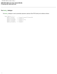
The Flash Memory and EMIF-B are shown in Figure 3.
Flash
Memory
Da(15:0)
DSP
(EMIF-B)
Ctl
(20:1)
User FPGA
Adr(25:1)
(25:22)
x4
0V
Figure 3 Flash Memory and EMIF-B
4.6.2.3. Serial Memory
A 1k-bit 1-wire EEPROM (type Dallas DS2432) is connected to the User FPGA. This device
contains a write-only secret and 512-bit SHA engine. Please see the manufacturer’s
datasheet for more information on this device.
4.6.3. Video Interfaces
The card has six triple-rate SDI interfaces (four transmit and two receive). Each interface
uses a MGT link on the FPGA running at 2.97Gb/s or 2.967 Gb/s.
Reference designs using the MGTs for SD-, HD-, 3G-SDI and DVB-ASI are available from
Xilinx.
4.6.3.1. Reference Clocks
Two reference oscillators are connected to GTPREFCLK inputs on the user FPGA. These
run at 148.5MHz and 148.3516484MHz.
ADM-AMC-5A2 User Manual
Version 1.0
Page 9
ADM-AMC-5A2 User Manual
4.6.3.2. Transmit
The transmit interfaces use MGT outputs connected to Gennum GS2978 line drivers and 75
Ohm SMB connectors on the front-panel. The connections are shown in Table 4.
Channel
0
1
2
3
MGT
124_0
120_0
124_1
120_1
Connector
J6
J2
J5
J3
Table 4 Video Tx Channel connections
4.6.3.3. Receive
The receive interfaces use 75 Ohm front-panel connectors and Gennum GS2974 Cable
Equalisers. The equaliser outputs are connected to MGT inputs on the user FPGA. The
connections are shown in Table 5.
Channel
0
1
MGT
124_0
120_0
Connector
J1
J4
Table 5 Video Rx Channel connections
4.6.4. Ethernet
The User FPGA has two Gigabit Ethernet ports. Both use MGT connections for an SGMII link
to a Marvell 88E1112 PHY.
MGT 112_0 connects to RJ-45 connector U29 and MGT 112_1 connects to RJ-45 connector
U30.
4.7.
DSP
The TI DSP is connected both to the bridge FPGA for host access and to the User FPGA for
application specific processing.
The DSP is clocked at 50MHz and, by default, the board is configured to run the DSP core at
600 MHz. (x12 clock mode).
The DSP is configured to boot from the Host Port Interface.
4.7.1. Host Port Interface
The 32-bit Host Port Interface (HPI) provides access to the DSP through the bridge FPGA.
The HPI runs at a constant 50MHz and is asynchronous to the PCIe and Local Bus
interfaces.
4.7.2. ZBT Memory (EMIF A)
External Memory Interface A (EMIF-A) is connected to an 8MB (1M x 64) ZBT memory
component. The default frequency for the interface is 200MHz.
ADM-AMC-5A2 User Manual
Version 1.0
Page 10
ADM-AMC-5A2 User Manual
4.7.3. Flash Memory & User FPGA Interface (EMIF B)
The DSP has a connection to a 32MB Flash memory and the User FPGA on its EMIF-B
interface. See Sections 4.2 and 4.6.2.2 for further details.
4.7.4. Multi-Channel Buffered Serial Port (McBSP)
McBSP 0 and 1 are directly connected between the DSP and the User FPGA.
4.8.
Debug Daughterboard
4.8.1.
Xilinx JTAG
Ground
“
“
“
“
“
“
Pin
1
3
5
7
9
11
13
Pin
2
4
6
8
10
12
14
+3V3
XIL_TMS
XIL_TCK
XIL_TDO
XIL_TDI
n/c
n/c
Table 6 Debug Daughtercard J1, Xilinx JTAG
4.8.2.
MMC Microcontroller ICE
MMC_TCK
MMC_TDO
MMC_TMS
MP_3V3
MMC_TDI
Pin
1
3
5
7
9
Pin
2
4
6
8
10
Ground
MP_3V3
MMC_ICE_nRST
MMC_nRST
Ground
Table 7 Debug Daughtercard J5, MMC AVR ICE
4.8.3.
DSP XDS Emulator
DSP_TMS
DSP_TDI
DSP_PD
DSP_TDO
DSP_TCK_RET
DSP_TCK
DSP_EMU0
Pin
1
3
5
7
9
11
13
Pin
2
4
6
8
10
12
14
DSP_nTRST
Ground
NO PIN
n/c
Ground
“
“
Table 8 Debug Daughtercard J7, XDS Emulator
ADM-AMC-5A2 User Manual
Version 1.0
Page 11
ADM-AMC-5A2 User Manual
4.8.4.
MMC Serial Port
Tx
Rx
Ground
n/c
n/c
Pin
1
3
5
7
9
Pin
2
4
6
8
10
Ground
“
“
“
“
Table 9 Debug Daughtercard J2, MMC Serial Port
ADM-AMC-5A2 User Manual
Version 1.0
Page 12
ADM-AMC-5A2 User Manual
5.
Revision History
Date
Revision
Nature of Change
23-04-2008
0.1
Draft for comments.
24-04-2008
1.0
Initial Release
ADM-AMC-5A2 User Manual
Version 1.0
Page 13