1
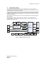
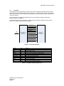
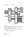
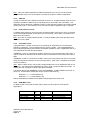
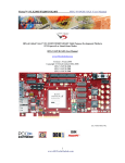
ADM-XRC-5TZ PCI Mezzanine Card User Guide Version 2.0 ADM-XRC-5TZ User Manual Copyright © 2007 - 2009 Alpha Data Parallel Systems Ltd. All rights reserved. This publication is protected by Copyright Law, with all rights reserved. No part of this publication may be reproduced, in any shape or form, without prior written consent from Alpha Data Parallel Systems Limited Alpha Data 4 West Silvermills Lane Edinburgh EH3 5BD UK Alpha Data 2570 North First Street, Suite 440 San Jose, CA 95131 USA Phone: Fax: Email: Phone: (408) 467 5076 Fax: (866) 820 9956 Email: [email protected] +44 (0) 131 558 2600 +44 (0) 131 558 2700 [email protected] ADM-XRC-5TZ User Manual Version 2.0 ADM-XRC-5TZ User Manual Table of Contents 1. 2. 3. 4. 5. 6. Introduction ........................................................................................................................1 1.1. Specifications ............................................................................................................1 Hardware Installation .........................................................................................................2 2.1. Handling instructions .................................................................................................2 2.2. Motherboard / Carrier requirements ..........................................................................2 2.3. PCI Mode selection ...................................................................................................2 2.4. Installing the ADM-XRC-5TZ onto a PMC motherboard ...........................................2 2.5. Installing the ADM-XRC-5TZ if fitted to an ADC-PMC ..............................................2 2.6. Cooling Requirements ...............................................................................................3 Software Installation ...........................................................................................................3 Board Description...............................................................................................................4 4.1. Local Bus ...................................................................................................................5 4.2. Flash Memory............................................................................................................6 4.2.1. Board Control Flash ..............................................................................................6 4.2.2. User FPGA Flash ..................................................................................................7 4.3. Health Monitoring ......................................................................................................8 4.3.1. Automatic Temperature Monitoring.......................................................................9 4.4. JTAG .........................................................................................................................9 4.4.1. Scan Chain Options ..............................................................................................9 4.4.2. FBS .......................................................................................................................9 4.5. Clocks ......................................................................................................................10 4.5.1. LCLK ...................................................................................................................10 4.5.2. REFCLK ..............................................................................................................11 4.5.3. PCIe Reference Clock ........................................................................................11 4.5.4. User MGT Clocks................................................................................................11 4.5.5. XRM MGT Clock .................................................................................................11 4.5.6. XRM Global Clock Input ......................................................................................12 4.5.7. XRM Regional Clocks .........................................................................................12 4.5.8. Rear (Pn4) Clocks ...............................................................................................12 4.5.9. PCI Clocks ..........................................................................................................12 4.6. User FPGA ..............................................................................................................13 4.6.1. Configuration .......................................................................................................13 4.6.2. I/O Bank Voltages ...............................................................................................13 4.6.3. Memory Interfaces ..............................................................................................13 4.7. XRM Bus and Front Panel I/O .................................................................................14 4.7.1. XRM Signalling Voltage ......................................................................................14 4.7.2. XRM Interface – Standard Signals and Power ...................................................15 4.7.3. XRM Interface – MGT Links ...............................................................................18 4.8. Pn4 I/O ....................................................................................................................19 4.8.1. Pn4 Signalling Voltage ........................................................................................19 4.9. XMC Interface .........................................................................................................20 4.9.1. Primary XMC Connector, P15 .............................................................................20 4.10. XRM IO146 Interface...............................................................................................21 XRM HSSDC2A Interface ................................................................................................23 Revision History ...............................................................................................................24 ADM-XRC-5TZ User Manual Version 2.0 ADM-XRC-5TZ User Manual Table of Tables Table 1 Local Bus Interface Signal List .................................................................................... 5 Table 2 Voltage and Temperature Monitors ............................................................................. 8 Table 4 MGT Clock Connections ............................................................................................ 11 Table 5 XRM Bus Regional Clocks......................................................................................... 12 Table 6 User FPGA I/O Bank Voltages .................................................................................. 13 Table 7 XRM I/O Voltage Selection ........................................................................................ 14 Table 8 XRM Interface - part 1 ............................................................................................... 15 Table 9 XRM Interface - part 2 ............................................................................................... 16 Table 10 XRM Interface - part 3 ............................................................................................. 17 Table 11 XRM Interface - MGT Links ..................................................................................... 18 Table 12 Pn4 to FPGA Assignments ...................................................................................... 19 Table 13 XMC P15 Connections ............................................................................................ 20 Table 14 IO146 Mictor Connector Pins 1 - 38 ........................................................................ 21 Table 15 IO146 Mictor Connector Pins 39 - 76 ...................................................................... 21 Table 16 IO146 Mictor Connector Pins 77 – 114.................................................................... 22 Table 17 IO146 Mictor Connector Pins 115 - 152 .................................................................. 22 Table 18 XRM-HSSDC2A-5T2 Pinout .................................................................................... 23 Table of Figures Figure 1 Figure 2 Figure 3 Figure 4 Figure 5 Figure 6 ADM-XRC-5TZ Block Diagram ................................................................................... 4 Local Bus Interface ..................................................................................................... 5 Board Control Flash Organisation .............................................................................. 6 Power-Up Configuration Sequence ............................................................................ 7 JTAG Header J3 ......................................................................................................... 9 Clock Structure ......................................................................................................... 10 ADM-XRC-5TZ User Manual Version 2.0 ADM-XRC-5TZ User Manual 1. Introduction The ADM-XRC-5TZ is a high performance PCI Mezzanine Card (PMC) designed for applications using the Virtex-5 FPGAs from Xilinx. This card supports all Virtex-5 LXT, SXT and FXT devices with the FFG1738 package. The card uses an FPGA PCI bridge developed by Alpha-Data supporting PCI-X and PCI. This allows high performance PCI-X / PCI operation without the need to integrate proprietary cores into the FPGA. A high-speed multiplexed address/data bus connects the bridge to the target (user) FPGA. The card can also be fitted with a Primary XMC connector to provide high-speed serial link connections to the user FPGA. 1.1. Specifications Physically conformant to VITA 42 XMC Standard Physically conformant to IEEE P1386-2001 Common Mezzanine Card standard (with XMC connector removed) 8-lane PCIe / Serial RapidIO connections to User FPGA (via XMC connector) 8 additional MGT links to User FPGA. (via front-panel adaptor) High performance PCI and DMA controllers Local bus speeds of up to 80 MHz Six independent banks of 2Mx36 ZBT SRAM (48MB total) User clock programmable between 31.25MHz and 625MHz Stable low-jitter 200MHz clock for precision IO delays User front panel adapter with up to 146 free IO signals User rear panel PMC connector with 6 free IO signals Programmable I/O voltage on front interface (1.8V / 2.5V / 3.3V) Supports 3.3V PCI or PCI-X at 64 bits ADM-XRC-5TZ User Manual Version 2.0 Page 1 ADM-XRC-5TZ User Manual 2. Hardware Installation This chapter explains how to install the ADM-XRC-5TZ onto a PMC motherboard or carrier. 2.1. Handling instructions Observe SSD precautions when handling the cards to prevent damage to components by electrostatic discharge. Avoid flexing the board. 2.2. Motherboard / Carrier requirements The ADM-XRC-5TZ is a 3.3V only PCI device and is not compatible with systems that use 5V signalling. The ADM-XRC-5TZ must be installed in a PMC motherboard or carrier that supplies +5.0V and +3.3V power to the PMC connectors. Ensure that this requirement is satisfied before powering it up. +12V and -12V may also be required for certain XRM modules. The current requirements on each power rail are highly dependent on the user FPGA application. A power estimator spreadsheet is available on request from Alpha Data. This should be used in conjunction with Xilinx power estimation tools to determine the exact requirements for each power rail. 2.3. PCI Mode selection Although the ADM-XRC-5TZ automatically detects whether the board is connected to a PCI or PCI-X bus, the default (initial) type is determined by Switch SW1D. If SW1D is OFF, the bridge FPGA will be configured for PCI-X mode after power-up and altered at PCI reset if a PCI bus is detected. If SW1D is ON, the bridge FPGA will be configured for PCI mode after power-up and altered at PCI reset if a PCI-X bus is detected. In most systems it is not essential to alter the position of this switch. However, systems with a PCIe interface in the User FPGA should load the user bitstream in to flash memory, set SW1D to match the bus type and enable the One-Time Configuration (OTC) feature (by setting SW1A to ON). See Section 4.2.1.2 for more details on OTC. 2.4. Note: Installing the ADM-XRC-5TZ onto a PMC motherboard This operation should not be performed while the PMC motherboard is powered up. The ADM-XRC-5TZ must be secured to the PMC motherboard using M2.5 screws in the four holes provided. The PMC bezel through which the I/O connector protrudes should be flush with the front panel of the PMC motherboard. 2.5. Installing the ADM-XRC-5TZ if fitted to an ADC-PMC The ADM-XRC-5TZ can be supplied for use in standard PC systems fitted to an ADC-PMC carrier board. The ADC-PMC can support up to two PMC cards whilst maintaining host PC PCI compatibility. If you are using a ADC-PMC, refer to the supplied documentation for information on jumper settings. All that is required for installation is a PCI slot that has enough space to accommodate the full-length card. The ADC-PMC is compatible with 5V and 3V PCI (32 and 64 bit) and PCI-X slots. It should be noted that the ADC-PMC uses a standard bridge to provide a secondary PCI bus for the ADM-XRC-5TZ and that some older BIOS code does not set up these devices correctly. Please ensure you have the latest version of BIOS appropriate for your machine. ADM-XRC-5TZ User Manual Version 2.0 Page 2 ADM-XRC-5TZ User Manual 2.6. Cooling Requirements The power consumption of the ADM-XRC-5TZ is highly dependent on the user FPGA application. With large FPGA applications, it is possible that the board may dissipate more than 15W. Although the board is designed to handle this, the user must ensure that it is adequately cooled. To prevent damage through over-heating, an on-board system monitor will automatically reconfigure the User FPGA with a low-power bitstream if the FPGA reaches 85°C or if the board reaches 70°C. (100°C and 85°C respectively for Industrial grade devices). The FPGA temperature may be measured using a software application or with Xilinx Chipscope and a JTAG cable. See Section 4.3 for further details of the on-board system monitor. 3. Software Installation Please refer to the Software Development Kit (SDK) installation CD. The SDK contains drivers, examples for host control and FPGA design and comprehensive help on application interfacing. ADM-XRC-5TZ User Manual Version 2.0 Page 3 ADM-XRC-5TZ User Manual 4. Board Description The ADM-XRC-5TZ follows the architecture of the ADM-XRC series and decouples the “target” FPGA from the PCI interface, allowing user applications to be designed with minimum effort and without the complexity of PCI design. A separate Bridge / Control FPGA interfaces to the PCI bus and provides a simpler Local Bus interface to the target FPGA. It also performs all of the board control functions including the configuration of the target FPGA, programmable clock setup and the monitoring of on-board voltage and temperature. ZBT SRAM and serial flash memory connect to the target FPGA and are supported by Alpha Data or Xilinx IP. IO functionality is provided using XRM modules. MGT links are connected through a SAMTEC QSE-DP connector, CN2. Remaining signals are connected through a 180 pin SAMTEC QSH connector, CN1. Config Flash Memory (32MB) Bridge Config Pn1 Pn2 Pn3 PCI-X / PCI64/66 User FPGA Bridge / Control FPGA (Virtex4 LX25) Local Bus (32 bit) Serial Flash (4MB) Pn4 Rear I/O (6 bit) Pn15 XMC PCIe / Serial RapidIO (x8) JTAG XRM Bus (146 bit) Programmable Clocks System Monitor (LM87) Virtex5 LXT/SXT/FXT (FFG1738) ZBT SRAM 8MB ZBT SRAM 8MB Power Conversion ZBT SRAM 8MB ZBT SRAM 8MB Figure 1 ADM-XRC-5TZ Block Diagram ADM-XRC-5TZ User Manual Version 2.0 Page 4 Front MGT (x8) Front I/O CN1 (XRM) ZBT SRAM 8MB ZBT SRAM 8MB ADM-XRC-5TZ User Manual 4.1. Local Bus The ADM-XRC-5TZ implements a multi-master local bus between the bridge and the target FPGA using a 32-bit multiplexed address / data path. The bridge design is asynchronous and allows the local bus to be run faster or slower than the PCI bus clock to suit the requirements of the user design. The local bus runs at 40MHz by default but this can be altered to different frequencies between 32MHz and 80MHz. Full details of the local bus operation, including timing constraints, DMA and Interrupts are given in the Software Development Kit (SDK). PCI Bus Bridge/Control FPGA Virtex4 LX25 lad_l[31:0] lbe_l[3:0] lads_l lblast_l lbterm_l lready_l lwrite ldreq_l[3:0] ldack_l[3:0] User FPGA Virtex5 LXT / SXT / FXT fhold fholda lreset_l lclk Figure 2 Local Bus Interface Signal lad[31:0] lbe_l[3:0] lads_l lblast_l lbterm_l lready_l lwrite ldreq_l[3:0] ldack_l[3:0] fhold fholda lreset_l lclk Type bidir bidir bidir bidir bidir bidir bidir unidir unidir unidir unidir unidir unidir Purpose Address and data bus. Byte qualifiers Indicates address phase Indicates last word Indicates ready and requests new address phase Indicates that target accepts or presents new data Indicates a write transfer from master DMA request from target to bridge DMA acknowledge from bridge to target Target bus request Bridge bus acknowledge Reset to target Clock to synchronise bridge and target Table 1 Local Bus Interface Signal List ADM-XRC-5TZ User Manual Version 2.0 Page 5 ADM-XRC-5TZ User Manual 4.2. Flash Memory The ADM-XRC-5TZ is fitted with two separate Flash memories: one connected to the Bridge / Control FPGA and the other to the User FPGA. 4.2.1. Board Control Flash A 256Mb Flash memory (Intel / Numonyx PC28F256P30) is used for storing Vital Product Data (VPD), programmable clock parameters and configuration bitstreams for the User FPGA. Access to this flash device is only possible through control logic registers. The flash is not directly mapped onto the local bus. Programming, erasing and verification of the flash are supported by the ADM-XRC SDK and driver. Utilities are provided to load bitstreams into the flash. These also verify the bitstream is compatible with the target FPGA. 0x0000_0000 Vital Product Data (VPD) 0x0000_03FE LCLK Word(15:0) 0x0000_0400 LCLK Word(31:16) 0x0000_0002 MCLK Word(15:0) 0x0000_0404 MCLK Word(31:16) 0x0000_0006 reserved B0 Length(7:0) Boot Flag 0 Bitstream 0 Length(23:8) 0x0080_0000 0x0080_0002 0x0082_0000 Target FPGA Bitstream 0 0x013F_FFFE B1 Length(7:0) Boot Flag 1 Bitstream 1 Length(23:8) Target FPGA Bitstream 1 “failsafe” 0x0140_0000 0x0140_0002 0x0142_0000 0x01FF_FFFE Figure 3 Board Control Flash Organisation ADM-XRC-5TZ User Manual Version 2.0 Page 6 ADM-XRC-5TZ User Manual 4.2.1.1. Power-Up Sequence If valid data is stored in the flash memory, the bridge will automatically set the programmable clock generators and configure the User FPGA at power-up. This sequence can be inhibited by shorting the FBS pin on JTAG connector J3 to GND. See the description of the “FBS” signal in Section 4.4 for further information. Note: If an over-temperature alert is detected from the System Monitor, the target will be reloaded with the alternate (failsafe) bitstream. Power Up 0 FBS N 1 N Bitstream Valid Y Config Tgt FPGA LCLK Wd Valid Y Y Set LCLK PCI Reset N MCLK Wd Valid Y Set MCLK Y One-Time Config N N N Reload Y Idle Figure 4 Power-Up Configuration Sequence 4.2.1.2. One-Time Configuration (OTC) If One-Time Configuration (OTC) is disabled (switch SW1A is OFF), the power-up configuration sequence will repeat each time PCI reset is asserted. If the OTC feature is enabled (switch SW1A is ON), the bridge will only set the clocks and configure the User FPGA at power-up. Once the sequence has completed, it will not repeat at PCI reset. Note: OTC only stops the user FPGA being reconfigured at PCI reset. If does not affect the manual reload function in the bridge control registers, or the over-temperature reload circuit. 4.2.2. User FPGA Flash An ST M25P32 flash memory with SPI interface is connected to the User FPGA for the storage of application-specific information. ADM-XRC-5TZ User Manual Version 2.0 Page 7 ADM-XRC-5TZ User Manual 4.3. Health Monitoring The ADM-XRC-5TZ has the ability to monitor temperature and voltage to maintain a check on the operation of the board. The monitoring is implemented by a National Semiconductor 2 LM87 and is supported by the Bridge FPGA control logic using I C. The Control Logic scans the LM87 when instructed by host software and stores the current voltage and temperature measurements in a blockram. This allows the values to be read without the need to communicate directly with the monitor. The following supplies and temperatures, as shown in Table 2, are monitored. Monitor 1.0V 1.2V 1.8V 2.5V 3.0V 3.3V 5.0V XRM_VCCIO Temp1 Temp2 Purpose User FPGA Core Supply Bridge FPGA Core Supply Memories, User FPGA Memory I/O, Local Bus I/O Config CPLD Core Supply Source voltage for Front, Rear I/O PCI VIO voltage (for Bridge FPGA) Board Input Supply Board Input Supply Either 2.5V or 3.3V Front Panel I/O Voltage User FPGA die temperature LM87 on die temperature for board/ambient Table 2 Voltage and Temperature Monitors An application is provided in the SDK that permits the reading of the health monitor. The typical output of the monitor is shown below, provided by the SYSMON program. *** SysMon *** FPGA Space Base Adr = 00900000 Control Space Base Adr = 00d00000 +1V0 +1V2 +1V8 +2V5 +3V0 +5V FPIO Reading Reading Reading Reading Reading Reading Reading = = = = = = = 1.01 1.21 1.81 2.51 3.01 5.04 3.34 SysMon Int Temp = User FPGA Temp = ADM-XRC-5TZ User Manual Version 2.0 Page 8 V V V V V V V 33 deg. C 26 deg. C ADM-XRC-5TZ User Manual 4.3.1. Automatic Temperature Monitoring At power-up, the control logic sets temperature limits and enables the over-temperature interrupt in the LM87. If the OTC feature is disabled, the limits and interrupt will be re-set after a PCI reset. If OTC is enabled, the limits and interrupt will only be set once at power-up. The temperature limits are shown in Table 3 below: Commercial Industrial User FPGA Min Max 0°C +85°C -40°C +100°C Board (LM87 internal) Min Max 0°C +70°C -40°C +85°C Table 3 Temperature Limits If any limit is exceeded, the User FPGA is automatically reconfigured with a low-power “failsafe” bitstream. The purpose of the failsafe mechanism is to protect the card from damage due to overheating. It is possible that the reconfiguration will cause the user application and, possibly, the host computer to hang. There are three ways to determine if the failsafe bitstream has been loaded: (1) Data bit (30) in the FPCTL control register will be set. (2) All local bus reads from the user FPGA will return 0xCAFEFABz, where z = Adr(2). (3) The device USERCODE (readable using JTAG) = 0x4144DEAD. 4.4. JTAG A JTAG header (J3) is provided to allow download of the FPGA using the Xilinx tools and serial download cables. This also allows the use of ChipScope PRO ILA to debug an FPGA design. TMS TDI TDO TCK FBS GND VCC Figure 5 JTAG Header J3 The VCC supply provided on J3 to the JTAG cable is +3.3V and is protected by a poly fuse with a rating of 350mA. 4.4.1. Scan Chain Options The devices in the scan chain can be altered for board test purposes using switch SW1C. The normal position for SW1C is open (off). In this position, four devices will be detected when the scan chain is initialised. If SW1C is closed (on), the ZBT memories will be included in the scan chain. 4.4.2. FBS The FBS signal is an input to the control logic and provides control of the cold boot process. By default, with no link fitted, the control logic will load a bitstream from flash into the FPGA if one is present. Shorting FBS to the adjacent GND pin will disable this process and can be used to recover situations where rogue bitstreams have been stored in flash. ADM-XRC-5TZ User Manual Version 2.0 Page 9 ADM-XRC-5TZ User Manual 4.5. Clocks The ADM-XRC-5TZ is provided with numerous clock sources, as shown in Figure 6 below: PCI Bus PCI RefClk PCI-X CLK Bridge Config (Coolrunner) Bridge FPGA (V4LX25) PCI CLK Zero-delay Buffer (PLL) XTAL_CLK REFCLK_200M 25.0 MHz XTAL 26.5625 MHz XTAL Ctl Femto-clock ICS843034-01 LCLK 200 MHz Osc. Local Bus USERMGT_CLKB USERMGT_CLKA PCIe_RefClk (100 MHz) XRM_MGTREF XRM_CLKIN XRM_PECL User FPGA Virtex5 LX220T / LX330T Pn4 Connector CLK0 (P) CLK1 (N) CLK2 (P) XRM Connector (Samtec) CLK3 (N) CLK4 (P) KEY CLK5 (N) Global Clock Inputs Clock Capable I/O MGT Clock Inputs CLK6 (P) CLK7 (N) Figure 6 Clock Structure 4.5.1. LCLK The Local Bus clock, LCLK, is generated from a 200MHz reference by a DCM within the bridge FPGA. The minimum LCLK frequency (determined by the DCM specification) is 32MHz. The maximum is 80MHz. The LCLK frequency is set by writing DCM multiply & divide values to the LCLOCK register in the bridge. (See SDK for details and example application). The default LCLK rate is 40MHz and is set on power-up. An alternative default rate can be stored in flash memory: FlashAdr 0x400 = DCM Multiplier Value – 1 FlashAdr 0x402 = DCM Divider Value – 1 ADM-XRC-5TZ User Manual Version 2.0 Page 10 ADM-XRC-5TZ User Manual Note: If the user FPGA application includes a DCM driven by LCLK (or one of the other programmable clocks), the clock frequency should be set prior to FPGA configuration. 4.5.2. REFCLK In order to make use of the IODELAY features of Virtex™-5, a stable low-jitter clock source is required to provide the base timing for tap delay lines in each IOB in the User FPGA. The ADM-XRC-5TZ is fitted with a 200MHz LVPECL (LVDS optional) oscillator connected to global clock resource pins. This reference clock can also be used for application logic if required. 4.5.3. PCIe Reference Clock A 100MHz PCIe reference clock input from the Primary XMC connector (Pn15) is connected to one of the dedicated MGT clock inputs on the user FPGA. (See Table 4 for details of the MGT clock connections.) Note: This clock is not generated on board. It is only available if the carrier provides it and connector Pn15 is fitted. 4.5.4. User MGT Clocks A programmable, low-jitter clock source is provided by an ICS843034-01 “FemtoClocks” frequency synthesiser. The synthesiser has two source crystals – one at 26.5625MHz (for Fibre Channel applications) and another at 25.0MHz (suitable for PCIe, Gigabit Ethernet etc.). The synthesiser also has two clock outputs. ”USERMGT_CLKA” is connected to an MGT clock input on the top-half of the user FPGA. It may be used as an alternative to the PCIe reference for the MGTs connected to the Primary XMC. ”USERMGT_CLKB” is connected to an MGT clock input on the bottom half of the user FPGA. It may be used as the reference for the front user MGTs. (See Table 4 for details of the MGT clock connections.) Note: Either of these clocks can provide a programmable source for applications that do not use MGTs. This requires the instantiation of a GTP_DUAL component within the FPGA. To simplify the task, a wrapper module is provided in the SDK. The default rate for both USERMGT_CLKA and USERMGT_CLKB is 250MHz and is set on power-up. An alternative default rate can be stored in flash memory: FlashAdr 0x404 = ClockWord(15:0) FlashAdr 0x406 = ClockWord(31:16) See the ICS843034-01 datasheet for details of the programming clock word. 4.5.5. XRM MGT Clock An XRM module can provide an MGT (GTP) reference clock input for user-specific applications. Clock Name PCIE_REFCLK USERMGT_CLKA XRM_MGTREF USERMGT_CLKB GTP No. 114 118 124 112 FPGA Pin (P/N) Reference for: AD4 / AD3 AK4 / AK3 C4 / C3 V4 / V3 Primary XMC (Pn15) MGTs Primary XMC (Pn15) MGTs Front (CN2) user MGTs Front (CN2) user MGTs Table 4 MGT Clock Connections ADM-XRC-5TZ User Manual Version 2.0 Page 11 ADM-XRC-5TZ User Manual 4.5.6. XRM Global Clock Input The XRM interface provides a differential input to the User FPGA global clocking resources. The default on-board terminations are suitable for an LVDS clock. 4.5.7. XRM Regional Clocks The XRM interface provides 8 clock lines that can be either be used single-ended or as 4 LVDS differential pairs. These clocks are routed to Clock-Capable inputs on the User FPGA, providing access to its regional clock capabilities. Each clock pair can be coupled with 16 pairs of XRM bus signals, as shown in Table 5 below: XRM Clocks 0 & 1 (Pair 0) 2 & 3 (Pair 1) 4 & 5 (Pair 2) 6 & 7 (Pair 3) FPGA Bank 15 11 13 17 XRM bus pairs 1 – 16 17 – 32 33 – 48 49 – 64 Table 5 XRM Bus Regional Clocks 4.5.8. Rear (Pn4) Clocks Two pairs of signals from Pn4 are connected to clock-capable inputs that can be used for regional clocking of the remaining Pn4 signals. See Table 12 for details. 4.5.9. PCI Clocks The PCI Interface within the bridge FPGA requires a regional clock input for 66MHz PCI operation or a global clock input for PCI-X. To comply with the single-load requirement in the PCI specification, a zero-delay clock buffer is used to route the PCI clock to the two different clock inputs. The clock buffer has a PLL with a minimum input frequency of 24MHz, potentially causing problems in applications that use the PCI 33MHz mode with a slow clock. In this case, the buffer can be bypassed to provide full PCI 33MHz compatibility. ADM-XRC-5TZ User Manual Version 2.0 Page 12 ADM-XRC-5TZ User Manual 4.6. User FPGA 4.6.1. Configuration The ADM-XRC-5TZ performs configuration from the host at high speed using SelectMAP. The FPGA may also be configured from flash or by JTAG via header J3. Download from the host is the fastest way to configure the User FPGA with 8 bit SelectMAP mode enabled. This permits an ideal configuration speed of up to 80MB/s. The ADM-XRC-5TZ can be configured to boot the User FPGA from flash on power-up if a valid bit-stream is detected in the flash. Booting from flash will also configure the programmable clocks. See Section 4.2.1.1. 4.6.2. I/O Bank Voltages Bank 0 1, 5, 6, 18, 19, 21, 23, 24, 25, 26 2 3, 4 11, 13, 15, 17 12, 20 Voltage 3.3V 2.5V 3.3V 2.5V 1.8V, 2.5V or 3.3V 2.5V Description Configuration I/F ZBT SRAM SelectMAP I/F, Pn4, Serial Flash Clocks, ZBT SRAM XRM Interface Local Bus Table 6 User FPGA I/O Bank Voltages 4.6.3. Memory Interfaces The ADM-XRC-5TZ has six independent banks of ZBT SRAM. Each bank has a 36 bit datapath. Data bits (35:32) are parity bits, where bit 32 is associated with bits (7:0) etc. The board will support higher capacity devices when they become available. 4.6.3.1. Memory Clocking Each memory bank has its own clock output from the target FPGA. To allow these clocks to be de-skewed, they are fed back into GCLK inputs on the FPGA. An example of this clock de-skewing method is shown in the “memory” application in the Alpha Data SDK. ADM-XRC-5TZ User Manual Version 2.0 Page 13 ADM-XRC-5TZ User Manual 4.7. XRM Bus and Front Panel I/O A major benefit of the ADM-XRC series of boards that use the XRM Bus interface is the versatility of I/O options that result. The ADM-XRC-5TZ maintains this interface and thus compatibility with a wide range of I/O modules to suit many diverse needs. Standard signals and power on the XRM interface use the 180 pin Samtec QSH series connector, CN1. MGT links use the 28 pin Samtec QSE-DP connector, CN2. 4.7.1. XRM Signalling Voltage The signalling voltage on the XRM connector (and User FPGA Banks 11, 13, 15 & 17) is selectable by jumper J2 J2 Link p1 & p2 Link p3 & p4 Link p5 & p4 XRM I/O voltage 3.3V 2.5V 1.8V Table 7 XRM I/O Voltage Selection ADM-XRC-5TZ User Manual Version 2.0 Page 14 ADM-XRC-5TZ User Manual 4.7.2. XRM Interface – Standard Signals and Power The XRM interface is implemented on CN1, a 180 pin Samtec connector type QSH, with the pin-out as detailed in tables Table 8 to Table 10. In turn, the signals that connect to CN1 are provided in the main from four banks of the User FPGA, Banks 11, 13, 15 & 17. These banks share a common VCCO that can be 1.8V, 2.5V or 3.3V powered, selectable with a jumper link on J3. Signal N_1 P_1 N_3 P_3 N_5 P_5 N_7 P_7 P_9 N_9 N_11 P_11 N_13 P_13 N_15 P_15 N_17 P_17 S_1 +3.3V +3.3V +3.3V +5V +5V VBAT +12V +12V PRESENCE_L XRM_TCK XRM_TMS FPGA Pin H39 H38 F40 F39 P37 R37 M39 N39 K38 J38 U38 T37 AA36 AA35 W35 Y35 G42 F42 R39 H39 H38 F40 F39 P37 R37 M39 N39 K38 J38 U38 Samtec Pin 1 3 5 7 9 11 13 15 17 19 21 23 25 27 29 31 33 35 37 39 41 43 45 47 49 51 53 55 57 59 Samtec Pin 2 4 6 8 10 12 14 16 18 20 22 24 26 28 30 32 34 36 38 40 42 44 46 48 50 52 54 56 58 60 FPGA Pin G39 G38 E39 E40 N38 P38 L39 M38 K40 K39 W38 V39 AA34 Y34 W36 W37 G41 F41 H40 J40 Table 8 XRM Interface - part 1 ADM-XRC-5TZ User Manual Version 2.0 Page 15 Signal N_2 P_2 P_4 N_4 N_6 P_6 N_8 P_8 P_10 N_10 N_12 P_12 P_14 N_14 P_16 N_16 N_18 P_18 CLK0 CLK1 XRM_SERID RESERVED XRM_VREF XRM_VCCIO XRM_VCCIO XRM_VCCIO -12V XRM_TDI XRM_TRST XRM_TDO ADM-XRC-5TZ User Manual Signal N_19 P_19 N_21 P_21 N_23 P_23 N_25 P_25 P_27 N_27 N_29 P_29 N_31 P_31 CLK2 CLK3 S_2 S_3 CLK4 CLK5 N_33 P_33 S_8 S_9 XRM_MGTREF_P XRM_MGTREF_N XRM_PECL_N XRM_PECL_P XRM_TX7_P XRM_TX7_N FPGA Pin J41 H41 M41 L42 P40 N40 AA39 AA40 P41 R40 V41 U42 Y42 W42 Y39 Y38 T39 L40 AE40 AD40 AB42 AB41 AK38 AG39 Samtec Pin 61 63 65 67 69 71 73 75 77 79 81 83 85 87 89 91 93 95 97 99 101 103 105 107 109 111 113 115 117 119 Samtec Pin 62 64 66 68 70 72 74 76 78 80 82 84 86 88 90 92 94 96 98 100 102 104 106 108 110 112 114 116 118 120 FPGA Pin K42 J42 N41 M42 Y40 W40 Y37 AA37 U41 T42 V40 W41 AA41 AA42 T40 AF40 AL42 AE37 AD42 AC41 AV40 AU39 AH39 Table 9 XRM Interface - part 2 ADM-XRC-5TZ User Manual Version 2.0 Page 16 Signal N_20 P_20 N_22 P_22 N_24 P_24 P_26 N_26 N_28 P_28 P_30 N_30 N_32 P_32 S_4 S_5 S_6 S_7 N_34 P_34 CLK6 CLK7 S_10 XRM_CLKIN_N XRM_CLKIN_P XRM_SDA XRM_SCL RESERVED XRM_RX7_P XRM_RX7_N ADM-XRC-5TZ User Manual Signal P_35 N_35 N_37 P_37 P_39 N_39 N_41 P_41 P_43 N_43 P_45 N_45 N_47 P_47 P_49 N_49 P_51 N_51 N_53 P_53 P_55 N_55 N_57 P_57 N_59 P_59 N_61 P_61 N_63 P_63 FPGA Pin AE42 AD41 AH41 AG42 AH40 AJ40 AC38 AB39 AL41 AK42 AP42 AP41 AU41 AT41 AB34 AC34 AC36 AD35 AE38 AE39 AG37 AF37 AT40 AR40 AK39 AJ38 AM39 AL39 AM38 AN38 Samtec Pin 121 123 125 127 129 131 133 135 137 139 141 143 145 147 149 151 153 155 157 159 161 163 165 167 169 171 173 175 177 179 Samtec Pin 122 124 126 128 130 132 134 136 138 140 142 144 146 148 150 152 154 156 158 160 162 164 166 168 170 172 174 176 178 180 FPGA Pin AF41 AF42 AJ42 AJ41 AB37 AB38 AC39 AC40 AN41 AM41 AT42 AR42 AC35 AB36 AV41 AU42 AD37 AD36 AG38 AF39 AP40 AN40 AR39 AT39 AH38 AJ37 AP38 AN39 AL37 AM37 Table 10 XRM Interface - part 3 ADM-XRC-5TZ User Manual Version 2.0 Page 17 Signal P_36 N_36 P_38 N_38 P_40 N_40 N_42 P_42 N_44 P_44 N_46 P_46 P_50 N_50 N_48 P_48 N_52 P_52 N_54 P_54 N_56 P_56 N_58 P_58 N_60 P_60 N_62 P_62 N_64 P_64 ADM-XRC-5TZ User Manual 4.7.3. XRM Interface – MGT Links Eight lanes of user MGT (GTP) links are routed to the XRM interface. Lanes 0 – 6 are routed through Samtec QSE-DP connector, CN2. Lane 7 is routed through the Samtec QSH connector, CN1. Signal XRM_TX0_P XRM_TX0_N XRM_RX0_P XRM_RX0_N XRM_TX1_P XRM_TX1_N XRM_RX1_P XRM_RX1_N XRM_TX2_P XRM_TX2_N XRM_RX2_P XRM_RX2_N XRM_TX3_P XRM_TX3_N XRM_RX3_P XRM_RX3_N XRM_TX4_P XRM_TX4_N XRM_RX4_P XRM_RX4_N XRM_TX5_P XRM_TX5_N XRM_RX5_P XRM_RX5_N XRM_TX6_P XRM_TX6_N XRM_RX6_P XRM_RX6_N XRM_TX7_P XRM_TX7_N XRM_RX7_P XRM_RX7_N FPGA Pin AA2 Y2 Y1 W1 T2 U2 U1 V1 R2 P2 P1 N1 K2 L2 L1 M1 J2 H2 H1 G1 D2 E2 E1 F1 B1 B2 A2 A3 B6 B5 A5 A4 GTP Number 112B “ “ “ 112A “ “ “ 116B “ “ “ 116A “ “ “ 120B “ “ “ 120A “ “ “ 124B “ “ “ 124A “ “ “ Samtec Pin 1 3 2 4 5 7 6 8 17 19 18 20 21 23 22 24 9 11 10 12 13 15 14 16 25 27 26 28 (CN1) 117 (CN1) 119 (CN1) 118 (CN1) 120 Table 11 XRM Interface - MGT Links ADM-XRC-5TZ User Manual Version 2.0 Page 18 ADM-XRC-5TZ User Manual 4.8. Pn4 I/O Up to 3 pairs of differential or 6 single-ended signals are available on Pn4 and are sourced from Bank 10 of the User FPGA. All of the signal traces are routed as 100 Ohm differential pairs and each pair is matched in length. The worst case difference in trace length between any two pairs is 10mm. Signal PN4_P1 PN4_N1 PN4_P3 PN4_N3 - FPGA Pin AK12 AK13 AM28 AL29 - Pn4 Pin 1 [CC] 3 [CC] 5 7 9 11 13 15 17 19 21 23 25 27 29 31 33 35 37 39 41 43 45 47 49 51 53 55 57 59 61 63 Pn4 Pin 2 [CC] 4 [CC] 6 8 10 12 14 16 18 20 22 24 26 28 30 32 34 36 38 40 42 44 46 48 50 52 54 56 58 60 62 64 FPGA Pin AJ30 AK30 - Signal PN4_P2 PN4_N2 - Table 12 Pn4 to FPGA Assignments In Table 12, pins marked [CC] are clock capable and may be used to access the regional clocking resources in the FPGA. 4.8.1. Pn4 Signalling Voltage The signalling voltage on the Pn4 is fixed at 3.3V ADM-XRC-5TZ User Manual Version 2.0 Page 19 ADM-XRC-5TZ User Manual 4.9. XMC Interface 4.9.1. Primary XMC Connector, P15 The MGT (GTP) links connected between the user FPGA and the Primary XMC connector, P15, are compatible with PCI Express and Serial RapidIO. Depending upon the carrier card, they may also be used for user-specific applications. Signal PCIE_TX0_P PCIE_TX0_N PCIE_RX0_P PCIE_RX0_N PCIE_TX1_P PCIE_TX1_N PCIE_RX1_P PCIE_RX1_N PCIE_TX2_P PCIE_TX2_N PCIE_RX2_P PCIE_RX2_N PCIE_TX3_P PCIE_TX3_N PCIE_RX3_P PCIE_RX3_N PCIE_TX4_P PCIE_TX4_N PCIE_RX4_P PCIE_RX4_N PCIE_TX5_P PCIE_TX5_N PCIE_RX5_P PCIE_RX5_N PCIE_TX6_P PCIE_TX6_N PCIE_RX6_P PCIE_RX6_N PCIE_TX7_P PCIE_TX7_N PCIE_RX7_P PCIE_RX7_N FPGA Pin AB2 AC2 AC1 AD1 AG2 AF2 AF1 AE1 AH2 AJ2 AJ1 AK1 AN2 AM2 AM1 AL1 AP2 AR2 AR1 AT1 AW2 AV2 AV1 AU1 BA1 BA2 BB2 BB3 BA6 BA5 BB5 BB4 GTP Number 114A “ “ “ 114B “ “ “ 118A “ “ “ 118B “ “ “ 122A “ “ “ 122B “ “ “ 126A “ “ “ 126B “ “ “ Table 13 XMC P15 Connections ADM-XRC-5TZ User Manual Version 2.0 Page 20 P15 Pin A1 B1 A11 B11 D1 E1 D11 E11 A3 B3 A13 B13 D3 E3 D13 E13 A5 B5 A15 B15 D5 E5 D15 E15 A7 B7 A17 B17 D7 E7 D17 E17 ADM-XRC-5TZ User Manual 4.10. XRM IO146 Interface The following tables provide the user with information on the pin-out of the XRM-IO146 when fitted to an ADM-XRC-5TZ version card. The signal names P_1/N_1 etc are internal to the ADM-XRC-5TZ. The important mapping is between the Mictor pin and the FPGA pin. Signal P_1 N_1 P_3 N_3 P_5 N_5 P_7 N_7 P_9 N_9 P_11 N_11 P_13 N_13 P_15 N_15 S_1 S_2 +5V FPGA Pin Samtec H38 H39 F39 F40 R37 P37 N39 M39 K38 J38 T37 U38 AA35 AA36 Y35 W35 R39 T39 Mictor Pin 3 1 7 5 11 9 15 13 17 19 23 21 27 25 31 29 37 93 Mictor Pin 1 3 5 7 9 11 13 15 17 19 21 23 25 27 29 31 33 35 37 - Samtec 2 4 6 8 10 12 14 16 18 20 22 24 26 28 30 32 34 36 38 FPGA Pin 6 8 4 2 12 10 16 14 18 20 24 22 26 28 30 32 38 40 90 E39 E40 G38 G39 P38 N38 M38 L39 K40 K39 V39 W38 AA34 Y34 W36 W37 H40 J40 T40 Signal P_4 N_4 P_2 N_2 P_6 N_6 P_8 N_8 P_10 N_10 P_12 N_12 P_14 N_14 P_16 N_16 CLK0 CLK1 S_4 Table 14 IO146 Mictor Connector Pins 1 - 38 Signal P_17 N_17 P_19 N_19 P_21 N_21 P_23 N_23 P_25 N_25 P_27 N_27 P_29 N_29 P_31 N_31 S_8 S_9 +5V FPGA Pin Samtec F42 G42 H41 J41 L42 M41 N40 P40 AA40 AA39 P41 R40 U42 V41 W42 Y42 AK38 AG39 35 33 63 61 67 65 71 69 75 73 77 79 83 81 87 85 105 107 - Mictor Pin Mictor Pin 39 41 43 45 47 49 51 53 55 57 59 61 63 65 67 69 71 73 75 Samtec 40 42 44 46 48 50 52 54 56 58 60 62 64 66 68 70 72 74 76 FPGA Pin 36 34 64 62 68 66 72 70 74 76 80 78 82 84 88 86 89 91 95 Table 15 IO146 Mictor Connector Pins 39 - 76 ADM-XRC-5TZ User Manual Version 2.0 Page 21 F41 G41 J42 K42 M42 N41 W40 Y40 Y37 AA37 T42 U41 V40 W41 AA42 AA41 Y39 Y38 L40 Signal P_18 N_18 P_20 N_20 P_22 N_22 P_24 N_24 P_26 N_26 P_28 N_28 P_30 N_30 P_32 N_32 CLK2 CLK3 S_3 ADM-XRC-5TZ User Manual Signal P_33 N_33 P_35 N_35 P_37 N_37 P_39 N_39 P_41 N_41 P_43 N_43 P_45 N_45 P_47 N_47 S_5 S_6 +5V FPGA Pin Samtec AB41 AB42 AE42 AD41 AG42 AH41 AH40 AJ40 AB39 AC38 AL41 AK42 AP42 AP41 AT41 AU41 AF40 AL42 Mictor Pin 103 101 121 123 127 125 129 131 135 133 137 139 141 143 147 145 92 94 Mictor Pin 77 79 81 83 85 87 89 91 93 95 97 99 101 103 105 107 109 111 113 - Samtec 78 80 82 84 86 88 90 92 94 96 98 100 102 104 106 108 110 112 114 FPGA Pin 100 98 122 124 126 128 130 132 136 134 140 138 144 142 152 150 97 99 AC41 AD42 AF41 AF42 AJ42 AJ41 AB37 AB38 AC40 AC39 AM41 AN41 AR42 AT42 AU42 AV41 AE40 AD40 - Signal P_34 N_34 P_36 N_36 P_38 N_38 P_40 N_40 P_42 N_42 P_44 N_44 P_46 N_46 P_48 N_48 CLK4 CLK5 +5V Table 16 IO146 Mictor Connector Pins 77 – 114 Signal P_49 N_49 P_51 N_51 P_53 N_53 P_55 N_55 P_57 N_57 P_59 N_59 P_61 N_61 P_63 N_63 S_7 S_10 +5V FPGA Pin Samtec AB34 AC34 AC36 AD35 AE39 AE38 AG37 AF37 AR40 AT40 AJ38 AK39 AL39 AM39 AN38 AM38 AE37 AH39 149 151 153 155 159 157 161 163 167 165 171 169 175 173 179 177 96 106 - Mictor Pin Mictor Pin 115 117 119 121 123 125 127 129 131 133 135 137 139 141 143 145 147 149 151 Samtec 116 118 120 122 124 126 128 130 132 134 136 138 140 142 144 146 148 150 152 FPGA Pin 146 148 156 154 160 158 164 162 168 166 172 170 176 174 180 178 102 104 - Table 17 IO146 Mictor Connector Pins 115 - 152 ADM-XRC-5TZ User Manual Version 2.0 Page 22 AC35 AB36 AD36 AD37 AF39 AG38 AN40 AP40 AT39 AR39 AJ37 AH38 AN39 AP38 AM37 AL37 AV40 AU39 Signal P_50 N_50 P_52 N_52 P_54 N_54 P_56 N_56 P_58 N_58 P_60 N_60 P_62 N_62 P_64 N_64 CLK6 CLK7 +5V ADM-XRC-5TZ User Manual 5. XRM HSSDC2A Interface Signal XRM_TX0_P XRM_TX0_N XRM_TX1_P XRM_TX1_N XRM_TX2_P XRM_TX2_N XRM_TX3_P XRM_TX3_N XRM_RX0_P XRM_RX0_N XRM_RX1_P XRM_RX1_N XRM_RX2_P XRM_RX2_N XRM_RX3_P XRM_RX3_N FPGA Pin AA2 Y2 T2 U2 R2 P2 K2 L2 Y1 W1 U1 V1 P1 N1 L1 M1 GTP Number 112B “ 112A “ 116B “ 116A “ 112B “ 112A “ 116B “ 116A “ Samtec Pin CN2-1 CN2-3 CN2-5 CN2-7 CN2-17 CN2-19 CN2-21 CN2-23 CN2-2 CN2-4 CN2-6 CN2-8 CN2-18 CN2-20 CN2-22 CN2-24 Table 18 XRM-HSSDC2A-5T2 Pinout ADM-XRC-5TZ User Manual Version 2.0 Page 23 XRM Pin P1-6 P1-5 P2-6 P2-5 P3-6 P3-5 P4-6 P4-5 P1-2 P1-3 P2-2 P2-3 P3-2 P3-3 P4-2 P4-3 ADM-XRC-5TZ User Manual 6. Revision History Date Revision Nature of Change 18-07-2008 1.0 Initial release. 04-08-2008 1.1 Modified SysMon voltage description for PCI VIO (+3V0) 13-08-2008 1.2 Removed references to XRC-5T2, updated description for MCLK usage. 31-08-2009 2.0 1.1: Added Front I/O voltages, 2.2: Added note on power estimation and current requirements, 2.3: New section on PCI mode selection, 2.6: New section on cooling requirements, 4.2.1: Added diagram of flash organisation, 4.2.1.1: New section on power-up sequence, 4.2.1.2: New section on One-Time Configuration feature, 4.3.1: New section on Automatic Temperature Monitoring, 4.5.1: Added note on default LCLK rate, 4.5.3: Note on PCIe Clock availability, 4.5.4: Note on MGT clock defaults. ADM-XRC-5TZ User Manual Version 2.0 Page 24