1
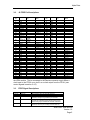
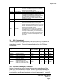
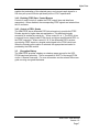
XRM-FPDP
Front Panel Data Port I/O Module
User Manual
Version 1.0
Alpha Data
Copyright © 2008 Alpha Data Parallel Systems Ltd. All rights reserved.
This publication is protected by Copyright Law, with all rights reserved. No part of this
publication may be reproduced, in any shape or form, without prior written consent from
Alpha Data Parallel Systems Limited
Reserved rights
This manual is designed to provide outline information only. Alpha Data has a
continual policy of improving its products; hence it reserves the right to change
product specification without prior warning. Alpha Data cannot accept any
liability for loss or damages arising from the use of this manual or the use of
products detailed within it.
Warranty and Support
All Alpha Data products enjoy parts and labor warranty for 12 months after
purchase. The warranty is based on the customer returning the defective goods
to Alpha Data for repair or replacement, which will be at the discretion of the
company. The warranty does not cover damages caused by negligence,
misuse, and normal wear and tear. No liability is accepted by the company for
any damage caused by the use of its hardware or software.
All goods from Alpha Data carry a 6 months free support service. This service is
available by letter, phone, fax, and email. Technical support contracts for longer
periods are available on request. Support contracts for software components
also normally cover the cost of upgrades.
Alpha Data
4 West Silvermills Lane
Edinburgh EH3 5BD
UK
Alpha Data
2570 North First Street, Suite 440
San Jose, CA 95131
USA
Phone:
Fax:
Email:
Phone: (408) 467 5076
Fax:
(866) 820 9956
Email: [email protected]
+44 (0) 131 558 2600
+44 (0) 131 558 2700
[email protected]
XRM-FPDP User Manual
Version 1.0
Page 2
Alpha Data
Table of Contents
1.
Introduction............................................................................................... 4
1.1. Standards ............................................................................................. 4
2. Installation ................................................................................................ 4
2.1. Handling instructions ............................................................................ 4
2.2. Board Jumper Settings......................................................................... 4
3. Module Description................................................................................... 4
3.1. FPDP Interface..................................................................................... 4
3.2. J2 FPDP Pin Descriptions .................................................................... 5
3.3. FPDP Signal Descriptions .................................................................... 5
3.4. XRM Control signals............................................................................. 6
3.4.1.
Control of FPDP Signal Termination ............................................... 6
3.4.2.
Enabling FPDP Data / Control Busses............................................ 7
3.4.3.
Control of PECL Strobe................................................................... 7
3.5. Encryption Battery ................................................................................ 7
XRM-FPDP User Manual
Version 1.0
Page 3
Alpha Data
1.
Introduction
XRM I/O modules allow for re-configurable connectivity solutions using specific
connectors and I/O standards. This modular approach allows for specific
interfaces to be employed on common FPGA platforms.
The XRM-FPDP is a front panel adapter module designed for use with Alpha
Data’s FPGA based XRC boards. It can function as a receiver or transmitter of
FPDP data. The Front Panel Data Port (FPDP) bus is intended to provide data
transfer between two or more boards at up to 160MB/s with the lowest possible
latency. The FPDP bus is a 32-bit parallel synchronous bus wired by means of
an 80-conductor ribbon cable.
1.1. Standards
ANSI/VITA 17-1998 (R2004)
2.
Installation
The XRM-FPDP is designed to plug into the front panel connector (SAMTEC
QSH series) of an Alpha Data FPGA card. The retaining screws should be
tightened to secure the XRM-FPDP.
Note: This operation should not be performed while the host PMC or PCI
card is powered up.
2.1. Handling instructions
Observe ESD precautions when handling the modules to prevent damage to
components by electrostatic discharge. Avoid flexing the board.
2.2. Board Jumper Settings
The XRM-FPDP uses a 3.3V signalling voltage with the FPGA board. The
proper setting must be made on the XRC host board for the front I/O voltage;
typically done via a switch or jumper on the XRC board.
3.
Module Description
The XRM-FPDP IO module provides connection to Front Panel Data Port
interfaces. It uses the standard 80 way KEL 8831E-080-170L or RN P50E-080P1-SR1-TG connector with Non Inverted FPDP pin assignments described in
VITA17.
3.1. FPDP Interface
The XRM-FPDP utilizes bi-directional bus switches for all electrical connections
to the J2 FPDP connector. This provides 5V signalling level tolerance and
translates the signalling voltage to 3.3V for the FPGA connections.
XRM-FPDP User Manual
Version 1.0
Page 4
Alpha Data
3.2.
J2 FPDP Pin Descriptions
FPDP
Pin
1
3
5
7
9
11
13
15
17
19
21
23
25
Function
27
GND
GND
GND
Nrdy
Dir
Reserved
Suspend
GND
PIO2
PIO1
Reserved
Resreved
Pstrobe
+ve
Pstrobe -ve
29
31
33
35
37
39
41
43
45
47
49
51
53
55
57
59
61
63
65
67
69
71
73
75
77
79
Sync
Dvalid
D31
GND
D28
D27
GND
D24
D23
GND
D20
D19
GND
D16
D15
GND
D12
D11
GND
D08
D07
GND
D04
D03
GND
D00
J1 Samtec
Pin
77
73
74
63
64
89 (in) or
91(out)
89 (in) or
91(out)
61
62
37
34
33
30
29
26
25
22
21
18
17
14
13
10
9
6
XRM Bus
Name
IO_50P_1
IO_72N_1
IO_71P_1
IO_73P_1
IO_68P_1
*
FPDP
Pin
2
4
6
8
10
12
14
16
18
20
22
24
26
Function
Strob
GND
GND
GND
GND
GND
GND
GND
GND
GND
GND
GND
GND
J1 Samtec
Pin
38
-
XRM Bus
Name
CLK0
-
*
28
GND
-
-
IO_73N_1
IO_68N_1
IO_51P_1
IO_26N_1
IO_49N_1
IO_20P_1
IO_22N_1
IO_29P_1
IO_28N_1
IO_2N_1
IO_25N_1
IO_23P_1
IO_3P_1
IO_54N_1
IO_5N_1
IO_52N_1
IO_6N_1
IO_30P_1
30
32
34
36
38
40
42
44
46
48
50
52
54
56
58
60
62
64
66
68
70
72
74
76
78
80
GND
GND
D30
D29
GND
D26
D25
GND
D22
D21
GND
D18
D17
GND
D14
D13
GND
D10
D09
GND
D06
D05
GND
D02
D01
GND
36
35
32
31
28
27
24
23
20
19
16
15
12
11
8
7
-
IO_26P_1
IO_49P_1
IO_20N_1
IO_22P_1
IO_29N_1
IO_28P_1
IO_2P_1
IO_25P_1
IO_23N_1
IO_3N_1
IO_54P_1
IO_5P_1
IO_52P_1
IO_6P_1
IO_30N_1
IO_19P_1
-
* Note: the Pstrobe +/- differential PECL signal connects to a driver/receiver on
the XRM module. This is connected to the Samtec connector on pin 89 as a
clock input to the FPGA or on pin 91 as a clock output from the FPGA. (see
control signals in section 3.4.3)
3.3.
FPDP Signal Descriptions
SIGNAL
D<31:00>
DIR*
DVALID*
NAME
Data Bus
Data Direction
Data Valid
STROB
Data Strobe
NRDY*
Not Ready
COMMENTS
32-bit data bus driven by FPDP/TM Interfaces.
The FPDP/TM asserts DIR* low.
When asserted, DVALID* indicates that the data bus has
valid data. This signal is generated by the FPDP/TM.
STROB is a free running clock supplied by the FPDP/TM.
FPDP/R and FPDP/RM interfaces should sample the data
with the rising edge of STROB when DVALID* is asserted.
NRDY* should be asserted by FPDP/R or FPDP/RM
interfaces, when they are not ready to receive data. The
XRM-FPDP User Manual
Version 1.0
Page 5
Alpha Data
PIO1, PIO2
Programmable I/O
PSTROBE
+PECL Data Strobe
PSTROBE*
-PECL Data Strobe
Reserved
SUSPEND*
Suspend Data
SYNC*
Sync Pulse
FPDP/TM should sample this signal until the FPDP/R or
FPDP/RM brings it high, at which time the transfer should
commence. Since NRDY* is asynchronous to STROB, the
FPDP/TM should double-synchronize to it before sampling its
state; this avoids metastability problems.
The PIO signals are programmable I/O lines. They may be
configured as inputs or outputs.
This signal along with PSTROBE* may be generated by the
FPDP/TM as an optional differential ±PECL data strobe.
PSTROBE is the positive version of the differential clock and
has the same polarity as STROB. For high data rate
applications, the differential ±PECL data strobe should be
used instead of STROB.
This signal is the negative version of the differential PECL
data strobe.
No connection should be made to reserved signals.
SUSPEND* should be generated by FPDP/R or FPDP/RM
interfaces to inform the data source of a pending buffer
overflow condition. The FPDP/TM may delay for no more than
16 cycles in total before suspending the transfer by negating
DVALID*. Since SUSPEND* is asynchronous to STROB, the
FPDP/TM should double-synchronize to it before sampling its
state; this avoids metastability problems.
The FPDP/TM must provide a Sync pulse to FPDP/R and
FPDP/RM interfaces to synchronize data transfers when
transmitting Single Frame data, Fixed Size Repeating Frame
data or Dynamic Size Repeating Frame data. FPDP/R and
FPDP/RM interfaces should wait for the Sync pulse before
accepting data. FPDP/R and FPDP/RM interfaces should
start to accept data on the first Data Valid period following the
Sync pulse.
3.4. XRM Control signals
There are 6 signals provided from the FPGA to the XRM-FPDP to control the
operation of the interface. This allows the module to be configured as a
transmitter or receiver. The control signal allocations from the FPGA are
shown below:
Signal
Control<0>
0:- Enable FPDP Control line termination
1:- Disable FPDP Control line termination
Pull-Up
0
0
J1
Samtec
Pin
67
Control<1>
0 :- Receiver terminations
1:- Transmitter termination
0 :- enable FPDP Control lines
1 :- Isolate FPDP Control lines
0 :- enable FPDP Data lines
1 :- Isolate FPDP Datal lines
0 :- enable FPDP PECL strobe
1 :- Disable FPDP PECL strobe
0 :- enable receive FPDP PECL strobe
1 :- enable transmit FPDP PECL strobe
Pull-Up
1
0
68
IO_76P_1
Pull-Up
0
0
65
IO_67N_1
Pull-Up
0
0
66
IO_76N_1
Pull-Up
0
0
69
IO_70N_1
Pull-Up
1
0
70
IO_53N_1
Control<2>
Control<3>
Control<4>
Control<5>
Description
H/W
Default
TX
Operation
RX
Operation
XRM Bus
Name
IO_67P_1
3.4.1. Control of FPDP Signal Termination
Control<1> selects the group of signals for termination depending on if the
XRM-FPDP is the transmitter or receiver. When it is the receiver, the signals
Dir and Strob are inputs and should be terminated. When it is the transmitter,
the signals Nrdy and Suspend are inputs and should be terminated. Control<0>
XRM-FPDP User Manual
Version 1.0
Page 6
Alpha Data
enables the termination of the selected group, and connects each signal to a
220 ohm pull-up and 330 ohm pull-down per the VITA17 specification.
3.4.2. Enabling FPDP Data / Control Busses
Control<2> and Control<3> enable the FPDP control lines and data lines
respectively. When disabled, the corresponding FPDP signals are isolated from
the J2 connector.
3.4.3. Control of PECL Strobe
The XRM-FPDP has a differential PECL driver/receiver to provide the FPDP
Pstrobe signals for higher data rate applications. This differential strobe
connection is enabled by control<4>. When control<5> is ‘1’ The PECL driver
is sourced from a single-ended FPGA signal, and driven as differential PECL to
the FPDP connector. When control<5> is ‘0’ the differential PECL receiver
converts the FPDP inputs to a singled ended signal to the FPGA clock input.
When the Pstrobe receive option is selected, the appropriate termination is
provided by the XRM module.
3.5. Encryption Battery
The XRM-FPDP provides a battery as a backup power source for the XRC
FPGA board encryption key. This is connected to VBATT of the target FPGA
via the J1 Samtec connector. For more information see the relevant Xilinx user
guide on using encrypted bitstreams.
XRM-FPDP User Manual
Version 1.0
Page 7