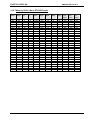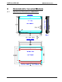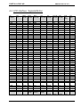
1
TECHNICAL USER'S MANUAL FOR: SmartModule Nordstrasse 11/F CH- 4542 Luterbach Tel.: ++41 (0)32 681 58 00 Fax: ++41 (0)32 681 58 01 Email: [email protected] Homepage: http://www.digitallogic.com SM520PC DIGITAL-LOGIC AG SM520PC Manual V1.1 COPYRIGHT 1999- 2003 BY DIGITAL- LOGIC AG No part of this document may be reproduced, transmitted, transcribed, stored in a retrieval system, in any form or by any means, electronic, mechanical, optical, manual, or otherwise, without the prior written permission of DIGITAL-LOGIC AG. The software described herein, together with this document, are furnished under a license agreement and may be used or copied only in accordance with the terms of that agreement. ATTENTION: All information in this manual and the product are subject to change without prior notice. REVISION HISTORY: Prod.-Serialnumber: From: To: Product BIOS Doc. Version Version Version V0.9 V1.0 V1.0 V1.1 1.26 V1.1 Date/Vis: 02.2003 KUF 05.2003 KUF 05.2003 DAR Modification: Remarks, News, Attention: Initial Version Revised Version, Preliminary PRODUCT REGISTRATION: Please register your product under: http://www.digitallogic.com -> SUPPORT After registration, you will receive driver & software updates, errata information, customer information and news from DIGITAL-LOGIC AG products automatically. 2 DIGITAL-LOGIC AG SM520PC Manual V1.1 Table of Contents 1 PREFACE .......................................................................................................... 5 1.1 1.2 1.3 1.4 1.5 1.6 1.7 1.8 1.9 2 How to use this manual....................................................................................................... 5 Trademarks........................................................................................................................... 5 Disclaimer............................................................................................................................. 5 Who should use this product ............................................................................................. 5 Recycling Information ......................................................................................................... 5 SMART Support Request Form (SMART-SRF) ................................................................. 6 smart DesignIn Center (smart – DIC)................................................................................. 7 Limited Warranty ................................................................................................................. 8 Sample Design Schematics ................................................................................................ 8 OVERVIEW ........................................................................................................ 9 2.1 2.2 2.3 2.4 2.5 2.6 2.7 2.8 2.9 2.10 3 Features ................................................................................................................................ 9 Unique Features................................................................................................................... 9 SM520PC block diagram ................................................................................................. 10 Specifications..................................................................................................................... 11 Ordering Codes.................................................................................................................. 13 BIOS History....................................................................................................................... 14 This product is “YEAR 2000 CAPABLE” ......................................................... 14 Related Application Notes ................................................................................................ 14 SM520PC Incompatibilities to a standard PC/AT ........................................................... 15 The smartModule520PC thermoanalysis ...................................................................... 17 PC FUNCTIONAL DESCRIPTION................................................................... 18 3.1 3.2 3.3 Interrupt Controllers.......................................................................................................... 18 PCI Devices and Definitions ............................................................................................. 18 Timers and Counters......................................................................................................... 19 3.3.1 Programmable Timers .................................................................................................. 19 3.3.2 Battery backed clock (RTC).......................................................................................... 20 3.3.3 Watchdog...................................................................................................................... 20 3.4 BIOS .................................................................................................................................... 21 3.4.1 ROM-BIOS ................................................................................................................... 21 3.4.2 EEPROM Memory for Setup ........................................................................................ 21 3.4.3 BIOS CMOS Setup....................................................................................................... 22 3.5 CMOS RAM Map................................................................................................................. 23 3.6 EEPROM saved CMOS Setup ........................................................................................... 29 3.7 Download the VGA-BIOS and the CORE-BIOS .............................................................. 30 3.8 Memory ............................................................................................................................... 31 3.8.1 System Memory Map.................................................................................................... 31 3.8.2 System I/O map............................................................................................................ 32 3.9 BIOS Data Area Definitions............................................................................................... 47 3.10 VGA, LCD............................................................................................................................ 54 3.10.1 VGA / LCD Controller 69000 ........................................................................................ 54 3.10.2 VGA / LCD BIOS for 69000 ........................................................................................ 54 3.10.3 Display Modes Supported ............................................................................................ 55 3.10.4 VGA/LCD BIOS Support............................................................................................... 56 3.10.5 Memory 69000 CRT/TFT Panels ................................................................................ 57 3.10.6 Memory 69000 Color STN-DD Panels ........................................................................ 58 3.10.7 Memory 69000 Mono STN-DD Panels........................................................................ 59 3.11 The Special Function Interface (SFI) ............................................................................... 60 3.11.1 INT 15h SFR Functions ................................................................................................ 60 3.12 Remote function................................................................................................................. 62 3.13 Remote Features................................................................................................................ 62 3.13.1 The Remote Server REMHOST.EXE........................................................................... 62 3.13.2 Remote enabler ............................................................................................................ 63 3.13.3 Cable Definition ............................................................................................................ 63 3.14 Watchdog Control.............................................................................................................. 64 3 DIGITAL-LOGIC AG 4 SM520PC Manual V1.1 DESCRIPTION OF THE JUMPERS................................................................. 65 5 LED CRITERIONS: .......................................................................................... 66 5.1 6 2 Power / control LEDs on the SM520PC .................................................................... 66 DESIGNIN WITH THE SMARTMODULE......................................................... 67 6.1 Mechanical Dimensions SM520PC .................................................................................. 67 6.1.1 Mechanical PCB Pad Dimensions on the Carrier-Board.............................................. 68 6.1.2 PCB to SM520PC height ............................................................................................ 69 6.1.3 Mechanical Dimensions of the PCB, plug .................................................................... 70 6.1.4 Mechanical Dimensions of the SM520PC, receptacle ................................................. 71 6.2 SM520PC uses signals on the smart480 bus............................................................... 72 6.3 LCD Interface Signaldefinition ........................................................................................ 78 6.4 CRT Monitor Signaldefinition .......................................................................................... 79 6.5 Connector Specifications ................................................................................................. 79 6.6 Thermal Specifications ..................................................................................................... 80 7 DESIGNIN BLOCK SCHEMATICS.................................................................. 81 7.1 The Chipsset ELAN520 from AMD .................................................................................. 82 7.1.1 Architecture overview ................................................................................................... 82 7.1.2 DRAM Interface ............................................................................................................ 83 7.1.3 PCI Interface................................................................................................................. 83 7.1.4 PCI Bus Signals............................................................................................................ 84 7.1.5 Design Considerations ................................................................................................. 84 7.1.6 PCI Signal Descripitons................................................................................................ 85 7.2 Powermanagement............................................................................................................ 87 7.3 Clocks ................................................................................................................................. 87 7.4 ITP / JTAG Signals............................................................................................................. 87 7.5 PCI Bus Signals ................................................................................................................. 88 7.6 ISA/EIO Signals .................................................................................................................. 89 7.7 USB Interface ..................................................................................................................... 90 7.8 IDE Interface ....................................................................................................................... 90 7.9 BIOS to Flash Memory Interface ...................................................................................... 91 8 ELAN520’S – BIOS........................................................................................ 91 9 SAMPLES SCHEMATICS SMXXPC- DK ....................................................... 91 10 INDEX .............................................................................................................. 96 4 DIGITAL-LOGIC AG 1 SM520PC Manual V1.1 PREFACE This manual is for integrators and programmers of systems based on the smartModule-520PC system on chip family. It contains information on hardware requirements, interconnections, and details of how to program the system. The specifications given in this manual were correct at the time of printing; advances mean that some may have changed in the meantime. 1.1 How to use this manual This manual is written for the original equipment manufacturer (OEM) who plans to build computer systems based on the system on chip units. It provides instructions for designing, installing and configuring the unit, and describes the system and setup requirements. 1.2 Trademarks Chips & Technologies MICROSPACE, MicroModule DOS Vx.y, Windows PC-AT, PC-XT NetWare Ethernet DR-DOS, PALMDOS ROM-DOS 1.3 SuperState R DIGITAL-LOGIC AG Microsoft Inc. IBM Novell Corporation Xerox Corporation Digital Research Inc. / Novell Inc. Datalight Inc. Disclaimer DIGITAL-LOGIC AG makes no representations or warranties with respect to the contents of this manual and specifically disclaims any implied warranty of merchantability or fitness for any particular purpose. DIGITALLOGIC AG shall under no circumstances be liable for incidental or consequential damages or related expenses resulting from the use of this product, even if it has been notified of the possibility of such damage. DIGITAL-LOGIC AG reserves the right to revise this publication from time to time without obligation to notify any person of such revisions 1.4 - Who should use this product Electronic engineers with know-how in PC-technology. Without electronic know-how we expect you to have questions. This manual assumes, that you have a general knowledge of PC-electronics. Because of the complexity and the variability of PC-technology, we can’t give any warranty that the product will work in any particular situation or combination. Pay attention to the electrostatic discharges. Use a CMOS protected workplace. Power supply OFF when you are working on the board or connecting any cables or devices. This is a high technology product. You need know-how in electronics and PC-technology to install the system ! 1.5 Recycling Information Hardware: - Print: epoxy with glass fiber wires are of tin-plated copper - Components: ceramics and alloys of gold, silver check your local electronic recycling 5 DIGITAL-LOGIC AG 1.6 SM520PC Manual V1.1 SMART Support Request Form (SMART-SRF) 1. Send this SRF with your problem description to: DIGITAL-LOGIC AG smartModule DesignIn Center Nordstr. 11/F CH-4542 Luterbach (SWITZERLAND) Fax: ++41 32 681 58 01 E-Mail: [email protected] Internet www.digitallogic.com Support request form (fill in and send via fax to DIGITAL-LOGIC AG support center): SRF No: S118_______ Date: Customer company: Customer Name: Customer Tel.No.: Customers Address: SMART type: Request type: Customer E-Mail: Customers Country: SM520PC Support Report: DesignIn Aid: BIOS Adaption: Manual Correction: others: processing date: Operating System: OS Version: BIOS Version: V___.____ V___.____ Problem description: Solution / Answer (will be filled in by DIGITAL-LOGIC AG SMART DesignIn center): Support date: Support sign: Support cost: DesignIn No.: yes no Support statistics: Comment: Offered costs for serving design support: Effective time / costs: 6 CHF/USD/DEM: DIGITAL-LOGIC AG 1.7 SM520PC Manual V1.1 smart DesignIn Center (smart – DIC) DIGITAL-LOGIC AG offers a DesignIn support from a specialized engineering group in the SMART DesignIn Center (SMART – DIC). To initialize a DesignIn Support, please fill in the SMART-SRF form. The DesignIn Support can be offered in each phase of a DesignIn procedure. Only the ordered support value will be charged. The charge fees are as follow: Design Phase No. Support type Fee Evaluation 01 02 03 Consultation Training Design of the customers specification CHF 200.-- per hour CHF 200.-- per hour CHF 150.-- per hour Schematics 10 11 12 13 Consultation Design of the schematics Review / Inspection of customers schematics Development of circuits / schematics CHF CHF CHF CHF 200.-150.-300.-200.-- per hour per hour per sheet per hour Layout 20 21 22 23 Consultation Design of the layout Review / Inspection of customers layout Development of circuits / layout CHF CHF CHF CHF 200.-150.-300.-200.-- per hour per hour per sheet per hour BIOS 30 31 32 33 Consultation Modification / Test of the BIOS sourcecode Review / Inspection of customers software Development of software CHF 200.-CHF 1500.-CHF 300.-CHF 200.-- per hour per day per hour per hour Prototype 40 41 42 43 Consultation Test of customers system Review / Inspection of customers system Development of test entvironment CHF 200.-CHF 1200.-CHF 300.-CHF 200.-- per hour per day per hour per hour All costs are payable in advance. 7 Charged DIGITAL-LOGIC AG 1.8 SM520PC Manual V1.1 Limited Warranty DIGITAL-LOGIC AG warrants the hardware and software products it manufactures and produces to be free from defects in materials and workmanship for one year following the date of shipment from DIGITAL-LOGIC AG, Switzerland. This warranty is limited to the original purchaser of product and is not transferable. During the one year warranty period, DIGITAL-LOGIC AG will repair or replace, at its discretion, any defective product or part at no additional charge, provided that the product is returned, shipping prepaid, to DIGITAL-LOGIC AG. All replaced parts and products become property of DIGITAL-LOGIC AG. Before returning any product for repair, customers are required to contact the company. This limited warranty does not extend to any product which has been damaged as a result of accident, misuse, abuse (such as use of incorrect input voltages, wrong cabling, wrong polarity, improper or insufficient ventilation, failure to follow the operating instructions that are provided by DIGITAL-LOGIC AG or other contingencies beyond the control of DIGITAL-LOGIC AG), wrong connection, wrong information or as a result of service or modification by anyone other than DIGITAL-LOGIC AG. Neither, if the user has not enough knowledge of these technologies or has not consulted the product manual or the technical support of DIGITAL-LOGIC AG and therefore the product has been damaged. Except, as expressly set forth above, no other warranties are expressed or implied, including, but not limited to, any implied warranty of merchantability and fitness for a particular purpose, and DIGITAL-LOGIC AG expressly disclaims all warranties not stated herein. Under no circumstances will DIGITAL-LOGIC AG be liable to the purchaser or any user for any damage, including any incidental or consequential damage, expenses, lost profits, lost savings, or other damages arising out of the use or inability to use the product. 1.9 Sample Design Schematics DIGITAL-LOGIC AG offers all schematics as a design guide only. DIGITAL-LOGIC AG assumes no responsibility for final system design. It is also assumed, that the designer has the reference manual of the ELAN520 (AMD) chip, the programmers reference from the ELAN520 chip. DIGITAL-LOGIC AG assumes, that the designer of a smartModule-520PC design, has the knowledge of designing ISA based PC architecture. 8 DIGITAL-LOGIC AG 2 OVERVIEW 2.1 Features SM520PC Manual V1.1 The smartModule-520PC is a miniaturized PC system on chip unit incorporating the major elements of a PC/AT compatible computer. It includes standard PC/AT compatible elements, such as: - Powerfull X86 with 133MHz clock BIOS ROM SODIMM socket for 16 - 128MB Timers DMA Real-time clock 2k EEPROM LPT1 COM1, COM2 Speaker interface AT-keyboard interface PS/2 mouse interface Floppydisk interface ATA-IDE harddisk interface channels VGA/LCD video controller Embedded smartBUS480 3.3V power supply (switched mode) 2.2 Unique Features - EEPROM for setup and configuration UL approved parts 2x USB Option: LAN 100/10Base-T as an assemblyoption - PCX 9 DIGITAL-LOGIC AG SM520PC Manual V1.1 2.3 SM520PC block diagram Chip CPU x86 DRAM BUS ELAN520Northbridge (SO-DIMM 16- 128MB) 32Bit PCI-BUS LCD/VGA VRAM Controller 2 MB 69000 ELAN520Southbridge Speaker RTC IDE LiBAT Watchdog 1232 EEPROM 2kByte LCD CRT 2x USB ISA-BUS BIOS 256kByte SMSC Super I/O MAX2ll IrDA FD LPT1 COM1 MAX2ll COM2 KB Mouse 10 DIGITAL-LOGIC AG 2.4 SM520PC Manual V1.1 Specifications CPU: CPU: Mode: Compatibility: 1. Level Cache: Word Size: Physical Addressing: Virtual Addressing: Clock Rates: ELAN520 133MHz from AMD Real / Protected 8086 – 80386 16 & 16kByte write-back 32 Bits 32 lines 128 Mbytes 133 MHz selectable Math. Coprocessor: Available on the CPU Power Management: available Defined by the BIOS 8237A comp. 2 channels 8 Bits DMA: Interrupts: 8259 comp. 8 + 2 levels PC compatible Timers: 8254 comp. 3 programmable counter/timers Memory: DRAM SODIMM32Bit 144pin holder (16 – 128Mbyte) 32Bit BUS ! external expandable up to 256Mbyte Controller: 69000 PCI-BUS CRT: 2Mbyte LCD: up to 1024 x 768 x 256 colors Panel: TFT 24Bit, STN, EL Plasma Video: Mass Storage: FD: HD: Flashdisk Floppy disk interface, for max. 2 floppy IDE interface, AT - Type, for max. 2 harddisks Optional: 2Mbyte with FFS, onmodule expandable up to 8MByte 11 DIGITAL-LOGIC AG SM520PC Manual V1.1 Standard AT Interfaces: Serial: Parallel: Keyboard: Mouse: Speaker: RTC: Backup current: Battery: Device Name COM1 COM2 FIFO Std.IRQs yes IRQ4 yes IRQ3 Addr. Signals: Remarks 3F8 2F8 (Baudrates: 50 – 115 KBaud programmable) LPT1 printer interface, Modes: SPP (output) , EPP ( bidir.) AT- or PS/2-keyboard PS/2 0.1 W output drive Integrated into the PIIX4 with CMOS-RAM 256byte <5 µA at 3V Not assembled Supervisory: Watchdog: LTC1232 with power-fail detection, strobe time max. 1 sec. ISA: Clock: PC/104plus Clock: USB DRAM IEEE-996 standard bus 8 MHz IEEE-996 standard bus, buffered 8 MHz defined by the Southbrisge 2 Channels SDRAM 32Bit ! BUS: Power Supply: Working: Power Rise Time: 5 Volts ± 5%, 3.3V onboard switch mode regulator > 100µs (0V --> 4,75V) Physical Characteristics: Dimensions: Length: Depth: Height: 85 mm +/- 0.1mm 66 mm +/- 0.1mm 16 mm +/- 0.2mm (with 5mm bus connectors) Weight: PCB Thickness: PCB Layer: 90 gr / 9 ounces 1.6 mm / 0.0625 inches nominal Multilayer Operating Environment: Relative Humidity: Vibration: Shock: Temperature: 5 - 90% non condensing 5 to 2000 Hz 10 G Operating: Standard version 133MHz: -25°C to +70###C Extended version: -40°C to +85°C T.B.D Storage: -55°C to +85 ###C 12 DIGITAL-LOGIC AG SM520PC Manual V1.1 EMI / EMC (IEC1131-2 refer MIL 461/462): ESD Electro Static Discharge: REF Radiated Electromagnetic Field: EFT Electric Fast Transient (Burst): SIR Surge Immunity Requirements: High-frequency radiation: IEC 801-2, EN55101-2, VDE 0843/0847 Part 2 metallic protection needed separate Ground Layer included 15 kV single peak IEC 801-3, VDE 0843 Part 3, IEC770 6.2.9. not tested IEC 801-4, EN50082-1, VDE 0843 Part 4 250V - 4kV, 50 ohms, Ts=5ns Grade 2: 1KV Supply, 500 I/O, 5Khz IEC 801-5, IEEE587, VDE 0843 Part 5 Supply: 2 kV, 6 pulse/minute I/O: 500 V, 2 pulse/minute FD, CRT: none EN55022 Any information is subject to change without notice. 2.5 Ordering Codes SM520PC SM520PCX SM520PCN smartModule520PC, 133MHz, Video, 0MByte smartModule520PC, 133MHz, Video, LAN, 0Mbyte smartModule520PC, 133MHz, no Video, no LAN, 0MByte SMxxPC-DK-32 smartModulexxPC Development-Kit with 32Mbyte DRAM 13 DIGITAL-LOGIC AG SM520PC Manual V1.1 2.6 BIOS History Version: 1.26 Date: 2003 2.7 This product is “YEAR 2000 CAPABLE” Status: Modifications: Serieproduction Inside-BIOS This DIGITAL-LOGIC product is “YEAR 2000 CAPABLE”. This means, that upon installation, it accurately stores, displays, processes, provides and/or receives date data from, into, and between 1999 and 2000, and the 20. and 21. centuries, including leap year calculations, provided that all other technology used in combination with said product properly exchanges date data with it. DIGITAL-LOGIC makes no representation about individual components within the product should be used independently from the product as a whole. You should understand that DIGITAL-LOGIC’s statement that an DIGITAL-LOGIC product is “YEAR 2000 CAPABLE” means only that DIGITAL-LOGIC has verified that the product as a whole meets this definition when tested as a stand-alone product in a test lab, but does not mean that DIGITAL-LOGIC has verified that the product is “YEAR 2000 CAPABLE” as used in your particular situation or configuration. DIGITAL-LOGIC makes no representation about individual components, including software, within the product should they be used independently from the product as a whole. DIGITAL-LOGIC customers use DIGITAL-LOGIC products in countless different configurations and in conjunction with many other components any systems, and DIGITAL-LOGIC has no way to test whether all those configurations and systems will properly handle the transition to the year 2000. DIGITAL-LOGIC encourages its customers and others to test whether their own computer systems and products will properly handle the transition to the year 2000. The only proper method of accessing the date in systems is indirectly from the Real-Time-Clock via the BIOS. The BIOS in DIGITAL-LOGIC computerboards contains a century checking and maintenance feature the checks the laest two significant digits of the year stored in the RTC during each BIOS request (INT 1A) to read the date and, if less than ‘80’ (i.e. 1980 is the first year supported by the PC), updates the century byte to ‘20’. This feature enables operating systems and applications using BIOS date/time services to reliably manipulate the year as a four-digit value. 2.8 Related Application Notes # Description Application Notes re availble at http://www.digitallogic.com ->support, or on any Application CD from DIGITAL-LOGIC. 14 DIGITAL-LOGIC AG SM520PC Manual V1.1 2.9 SM520PC Incompatibilities to a standard PC/AT - only 4 DMA – channels (DMA 0 – 3) no BUS-master signal only 11 IRQ lines available 15 DIGITAL-LOGIC AG SM520PC Manual V1.1 The smart480 bus , the future upgrade path DIGITAL-LOGIC produces different smartmodules using the smart480 bus. Since each module has some unique features, the integrator must use this signals carefully, if he likes to upgrade lateron with another module with a higher performance. The following performance will be available: 700Mhz 400MHz smP3PC-700 smP3PC-400 266Mhz smGXPC/X smP5PC 133Mhz 66Mhz sm520-PC sm520-PCX sm486PCX CPU 486SX 586DX Pentium I Pentium III CPU CPU-Clock Power consumption 486SX (ELAN400) 520PC 33-99Mhz 133Mhz 3 - 4 Watts 3 – 5 Watts Pentium I 166-266Mhz 5 – 7 Watts Pentium III 400-700Mhz 7 – 9 Watts Standard functions DRAM Expansion Keyboard & Mouse COM1 COM2 Floppydisk LPT1 Prim-DIE Sec-DIE ISA-Bus CRT-VGA Signals LCD 24Bit 32Bit yes yes yes yes yes yes no yes yes yes 32Bit yes yes yes yes yes yes yes yes yes yes 64Bit yes yes yes yes yes yes yes yes yes yes 64Bit yes yes yes yes yes yes yes yes yes yes Unique functions: PCCard LAN PCI-Bus Keymatrix 1/4VGA LCD 36Bit LCD Extension USB Interface COM3 ZV-Port yes yes no yes yes no no yes no no no yes no no yes no no no no no yes no no yes yes no no no no yes no no yes yes no no 16 DIGITAL-LOGIC AG 2.10 SM520PC Manual V1.1 The smartModule520PC thermoanalysis DIGITAL-LOGIC provides a set of thermal images, made after 120min operating in a typical applications. SM520PC Version 1.1 (run: MSDOS EDIT) Time: > 120 min. 17 DIGITAL-LOGIC AG SM520PC Manual V1.1 3 PC FUNCTIONAL DESCRIPTION 3.1 Interrupt Controllers An 8259A compatible interrupt controller, within the TX chipset, provides seven prioritized interrupt levels. Of these, several are normally associated with the board's onboard device interfaces and controllers, and several are available on the AT expansion bus. Interrupt: Sources: onboard used: IRQ0 ROM-BIOS clock tick function, from timer 0 IRQ1 Keyboard controller output buffer full IRQ2 Used for cascade 2. 8259 IRQ3 COM2 serial port IRQ4 COM1 serial port IRQ5 LPT2 parallel printer (if present) IRQ6 Floppy controller IRQ7 LPT1 parallel printer IRQ8 Battery backed clock IRQ9 Free for user IRQ10 Free for user IRQ11 Free for user IRQ12 PS/2 mouse IRQ13 Math. coprocessor IRQ14 Harddisk IDE / SCSI IRQ15 Free for user * It may depends on the LAN configuration yes yes yes yes yes no * yes yes yes no * no * no * yes yes yes no * 3.2 PCI Devices and Definitions The following definitions for the peripherals corresponds with the BIOS: Device: IDSEL PIRQ REQ# GNT# SLOT 1 AD20 A,B,C,D 0 0 SLOT 2 AD21 B,C,D,A 1 1 SLOT 3 AD22 C,D,A,B 2 2 SLOT 4 AD23 D,A,B,C 3 3 VGA Controller AD20 Option LAN-Controller AD29 IRQ-A 0 0 USB 82C861 AD26 IRQ-C 2 2 18 Comment: DIGITAL-LOGIC AG SM520PC Manual V1.1 3.3 Timers and Counters 3.3.1 Programmable Timers An 8253 compatible timer/counter device is also included in the board's ASIC device. This device is utilized in precisely the same manner as in a standard AT implementation. Each channel of the 8253 is driven by a 1.190 MHz clock, derived from a 14.318 MHz oscillator, which can be internally divided in order to provide a variety of frequencies. Timer 2 can also be used as a general purpose timer if the speaker function is not required. Timer Assignment Timer Function 0 1 2 ROM-BIOS clock tick (18.2 Hz) DRAM refresh request timing (15 µs) Speaker tone generation time base 19 DIGITAL-LOGIC AG SM520PC Manual V1.1 3.3.2 Battery backed clock (RTC) An AT compatible date/time clock is located within the chipset. The device also contains a CMOS static RAM, compatible with that in standard ATs. System configuration data is normally stored in the clock chip's CMOS RAM in a manner consistent with the convention used in other AT compatible computers. Connect an external Lithium battery of 3V to the RTC pin. The battery-backed clock can be set by using the DIGITAL-LOGIC AG SETUP at boot-time. Addresses: 70h 71h = = RTC-Address MAP: 00 - 0F 10 - 3F 40 - 7F Index register Data transfer register Real time clock BIOS setup (Standard) Extended BIOS With an external Lithium 3V- battery, the board is able to work over 10 years without replacing. The chip set consumes the following currents: Typical battery current at 25°C : <5 µA 3.3.3 Watchdog - The watchdog function is an implemented function of the ELAN520 and must be set/triggered by the application - Activate the Wachtdog in the bios setup - The watchdog is hardware triggered and will be activated also in case of a hanging system - The watchdog is programmable between 0.5ms and 32sec - The RESWDOG.CCP is a programming sample of how to do implement it into the customer's application. Any comments/explanations are integrated inside the file. See also chapter 3.12 20 DIGITAL-LOGIC AG SM520PC Manual V1.1 3.4 BIOS 3.4.1 ROM-BIOS An EPROM with 8 Bit wide data access normally contains the board's AT compatible ROM-BIOS. The BIOS takes a 29C020 EPROM (or equivalent) device. The board's wait-state control logic automatically inserts four memory wait states in all CPU accesses to this (socket). The ROM-BIOS occupies the memory area from C0000H through FFFFFh; however, the board's ASIC logic reserves the entire area from C0000h through FFFFFh for onboard devices, so that this area is already usable for ROM-DOS and BIOS expansion modules. Consult the appropriate address map for the MICROSPACE SM520PC ROM-BIOS. 3.4.1.1 Standard BIOS ROM DEVICE: 29C020 PLCC32 MAP: E0000 - FFFFFh C0000 - CBFFFh CC000 - CFFFFh Core-BIOS, 256kB onboard soldered VGA BIOS from Chips & Technology 32kB or 44kB reserved 3.4.2 EEPROM Memory for Setup The EEPROM is used for setup and configuration data, stored as an alternative to the CMOS-RTC. Optionally, the EEPROM setup driver may update the CMOS RTC, if the battery is running down and the checksum error would appear and stop the system. The capacity of the EEPROM is 2 kByte. Organisation of the 2048Byte EEPROMs: Address MAP: 0000h 0001h 0003h 0010h-007Fh 0080h-00FFh 0100h-010Fh 0110h-0113h 0114h-0117h 0118h-011Bh 011Ch-011Fh 0120h-0122h 0123h-0125h 0126h-0128h 0129h-012Bh 0130h 0131h 0132h/0133h 0134h/0135h 0136h 0137h 0200h-03FFh 0200h-027Fh 0400h-07FFh Function: CMOS-Setup valid (01=valid) Keymatrix-Setup valid (01=valid) Flag for DLAG-Message (FF=no message) Copy of CMOS-Setup data reserved for AUX-CMOS-Setup Serial-Number Production date (year/day/month) 1. Service date (year/day/month) 2. Service date (year/day/month) 3. Service date (year/day/month) Booterrors (Autoincremented if any booterror occurs) Setup Entries (Autoincremented on every Setup entry) Low Battery (Autoincremented everytime the battery is low, EEPROM -> CMOS) Startup (Autoincremented on every poweron start) Number of 512k SRAM Number of 512k Flash BIOS Version (V1.4 => [0132h]:= 4, [0133h]:=1) BOARD Version (V1.5 => [0124h]:=5, [0125h]:=1) BOARD TYPE (‘M’=PC/104, ‘E’=Euro, ‘W’=MSWS, ‘S’=Slot, ‘C’=Custom) CPU TYPE (01h=ELAN300/310, 02h=ELAN400, 03h=486SLC, 04h=486DX, 05h=P5). Keymatrix-Setup data Keymatrix Table Free for Customer’s use 21 DIGITAL-LOGIC AG SM520PC Manual V1.1 3.4.3 BIOS CMOS Setup If wrong setups are memorized in the CMOS-RAM, the default values will be loaded after resetting the RTC/CMOS-RAM with the CMOS-RESET jumper. If the battery is down, it is always possible to start the system with the default values from the BIOS. WARNING: On the next setup pages (switch with TAB) the values for special parameters are modifiable. Normally the parameters are set correctly by DIGITAL-LOGIC AG. Be very careful in modifying any parameter since the system could crash. Some parameters are dependent on the CPU type. The cache parameter is always available, for example. So, if you select too few wait states, the system will not start until you reset the CMOS-RAM using the RAM-Reset jumper, but the default values are reloaded. If you are not familiar with these parameters, do not change anything! 22 DIGITAL-LOGIC AG SM520PC Manual V1.1 3.5 CMOS RAM Map Systems based on the industry-standard specification include a battery backed Real Time Clock chip. This clock contains at least 64 bytes of non-volatile RAM. The system BIOS uses this area to store information including system configuration and initialization parameters, system diagnostics, and the time and date. This information remains intact even when the system is powered down. The BIOS supports 128 bytes of CMOS RAM. This information is accessible through I/O ports 70h and 71h. CMOS RAM can be divided into several segments: Locations 00h - 0Fh contain real time clock (RTC) and status information Locations 10h - 2Fh contain system configuration data Locations 30h - 3Fh contain System BIOS-specific configuration data as well as chipset-specific information Locations 40h - 7Fh contain chipset-specific information as well as power management configuration parameters The following table provides a summary of how these areas may be further divided. Beginning Ending Checksum Description 00h 10h 2Eh 30h 34h 40h 5Ch 5Eh 6Fh 7Eh 0Fh 2Dh 2Fh 33h 3Fh 5Bh 5Dh 6Eh 7Dh 7Fh No Yes No No No Yes No No Yes No RTC and Checksum System Configuration Checksum Value of 10h - 2Dh Standard CMOS Standard CMOS - SystemSoft Reserved Extended CMOS - Chipset Specific Checksum Value of 40h - 5Bh Extended CMOS - Chipset Specific Extended CMOS - Power Management Checksum Value of 6Fh - 7Dh 23 DIGITAL-LOGIC AG SM520PC Manual V1.1 Location 00h Description Time of day (seconds) specified in BCD 01h Alarm (seconds) specified in BCD 02h Time of Day (minutes) specified in BCD 03h Alarm (minutes) specified in BCD 04h Time of Day (hours) specified in BCD 05h Alarm (hours) specified in BCD 06h Day of week specified in BCD 07h Day of month specified in BCD 08h Month specified in BCD 09h Year specified in BCD 0Ah Status Register A Bit 7 = Update in progress Bits 6-4 = Time based frequency divider Bits 3-0 = Rate selection bits that define the periodic interrupt rate and output frequency. 0Bh Status Register B Bit 7 = Run/Halt 0 Run 1 Halt Bit 6 = Periodic Timer 0 Disable 1 Enable Bit 5 = Alarm Interrupt 0 Disable 1 Enable Bit 4 = Update Ended Interrupt 0 Disable 1 Enable Bit 3 = Square Wave Interrupt 0 Disable 1 Enable Bit 2 = Calendar Format 0 BCD 1 Binary Bit 1 = Time Format 0 12-Hour 1 24-Hour Bit 0 = Daylight Savings Time 0 Disable 1 Enable 0Ch Status Register C Bit 7 = Interrupt Flag Bit 6 = Periodic Interrupt Flag Bit 5 = Alarm Interrupt Flag Bit 4 = Update Interrupt Flag Bits 3-0 = Reserved 0Dh Status Register D Bit 7 = Real Time Clock 0 Lost Power 1 Power Continued... 24 DIGITAL-LOGIC AG CMOS Map SM520PC Manual V1.1 Continued... Location Description 0Eh CMOS Location for Bad CMOS and Checksum Flags bit 7 = Flag for CMOS Lost Power 0 1 bit 6 = = Power OK Lost Power = Flag for CMOS checksum bad 0 1 = = 0Fh Shutdown Code 10h Diskette Drives bits 7-4 = Diskette Drive A 0000 0001 0010 0011 0100 0101 = = = = = = Checksum is valid Checksum is bad Not installed Drive A = 360 K Drive A = 1.2 MB Drive A = 720 K Drive A = 1.44 MB Drive A = 2.88 MB bits 3-0 = Diskette Drive B 0000 0001 0010 0011 0100 0101 = = = = = = Not installed Drive B = 360 K Drive B = 1.2 MB Drive B = 720 K Drive B = 1.44 MB Drive B = 2.88 MB 11h Reserved 12h Fixed (Hard) Drives bits 7-4 = Hard Drive 0, AT Type 0000 = 0001-1110 1111 = Not installed Types 1 - 14 Extended drive types 16-44. See location 19h. bits 3-0 = Hard Drive 1, AT Type 0000 = 0001-1110 1111 = Not installed Types 1 - 14 Extended drive types 16-44. See location 2Ah. See the Fixed Drive Type Parameters Table in Chapter 2 for information on drive types 16-44. 13h Reserved Continued... 25 DIGITAL-LOGIC AG CMOS Map SM520PC Manual V1.1 Continued... Location Description 14h Equipment bits 7-6 = Number of Diskette Drives 00 = 01 = 10, 11 = One diskette drive Two diskette drives Reserved bits 5-4 = Primary Display Type 00 01 10 11 = = = = Adapter with option ROM CGA in 40 column mode CGA in 80 column mode Monochrome bits 3-2 = Reserved bit 1 = Math Coprocessor Presence 0 1 bit 0 = = Not installed Installed = Bootable Diskette Drive 0 1 = = Not installed Installed 15h Base Memory Size (in KB) - Low Byte 16h Base Memory Size (in KB) - High Byte 17h Extended Memory Size in (KB) - Low Byte 18h Extended Memory Size (in KB) - High Byte 19h Extended Drive Type - Hard Drive 0 See the Fixed Drive Type Parameters Table in Chapter 2 for information on drive types 16-44. 1Ah Extended Drive Type - Hard Drive 1 See the Fixed Drive Type Parameters Table in Chapter 2 for information on drive types 16-44. 1Bh Custom and Fixed (Hard) Drive Flags bits 7-6 = Reserved bit 5 = Internal Floppy Diskette Controller 0 1 bit 4 = = Disable Enabled = = Disable Enabled = Hard Drive 1 Custom Flag 0 1 bit 0 Disabled Enabled = Hard Drive 0 IDE Flag 0 1 bit 1 = = = Hard Drive 0 Custom Flag 0 1 bit 2 Disabled Enabled = Internal IDE Controller 0 1 bit 3 = = = = Disable Enabled = Hard Drive 1 IDE Flag 0 1 = = Disable Enabled Continued... 26 DIGITAL-LOGIC AG CMOS Map SM520PC Manual V1.1 Continued... Location Description 1Ch Reserved 1Dh EMS Memory Size Low Byte 1Eh EMS Memory Size High Byte 1Fh - 24h Custom Drive Table 0 These 6 bytes (48 bits) contain the following data: Cylinders Landing Zone Write Precomp Heads Sectors/Track 10 bits 10 bits 08 bits 1Fh Byte 0 bits 7-0 = Lower 8 Bits of Cylinders 20h Byte 1 bits 7-2 = Lower 6 Bits of Landing Zone bits 1-0 = Upper 2 Bits of Cylinders 21h Byte 2 bits 7-4 = Lower 4 Bits of Write Precompensation bits 3-0 = Upper 4 Bits of Landing Zone 22h Byte 3 bits 7-6 = Reserved bits 5-0 = Upper 6 Bits of Write Precompensation 23h Byte 4 bits 7-0 = Number of Heads 24h Byte 5 bits 7-0 = Sectors Per Track 25h - 2Ah Custom Drive Table 1 These 6 bytes (48 bits) contain the following data: Cylinders Landing Zone Write Precomp Heads Sectors/Track 10 bits 10 bits 08 bits 25h Byte 0 bits 7-0 = Lower 8 Bits of Cylinders 26h Byte 1 bits 7-2 = Lower 6 Bits of Landing Zone bits 1-0 = Upper 2 Bits of Cylinders 27h Byte 2 bits 7-4 = Lower 4 Bits of Write Precompensation bits 3-0 = Upper 4 Bits of Landing Zone Continued... 27 DIGITAL-LOGIC AG CMOS Map SM520PC Manual V1.1 Continued... Location Description 28h Byte 3 bits 7-6 = Reserved bits 5-0 = Upper 6 Bits of Write Precompensation 29h Byte 4 bits 7-0 = Number of Heads 2Ah Byte 5 bits 7-0 = Sectors Per Track 2Bh Boot Password bit 7 = Enable/Disable Password 0 1 = = Disable Password Enable Password bits 6-0 = Calculated Password 2Ch SCU Password bit 7 = Enable/Disable Password 0 1 = = Disable Password Enable Password bits 6-0 = Calculated Password 2Dh Reserved 2Eh High Byte of Checksum - Locations 10h to 2Dh 2Fh Low Byte of Checksum - Locations 10h to 2Dh 30h Extended RAM (KB) detected by POST - Low Byte 31h Extended RAM (KB) detected by POST - High Byte 32h BCD Value for Century 33h Base Memory Installed bit 7 = Flag for Memory Size 0 1 = = 640KB 512KB bits 6-0 = Reserved 34h Minor CPU Revision Differentiates CPUs within a CPU type (i.e., 486SX vs 486 DX, vs 486 DX/2). This is crucial for correctly determining CPU input clock frequency. During a power on reset, Reg DL holds minor CPU revision. 35h Major CPU Revision Differentiates between different CPUs (i.e., 386, 486, Pentium). This is crucial for correctly determining CPU input clock frequency. During a power on reset, Reg DH holds major CPU revision. 36h Hotkey Usage bits 7-6 = Reserved bit 5 = Semaphore for Completed POST bit 4 = Semaphore for 0 Volt POST (not currently used) bit 3 = Semaphore for already in SCU menu bit 2 = Semaphore for already in PM menu bit 1 = Semaphore for SCU menu call pending bit 0 = Semaphore for PM menu call pending 40h-7Fh Definitions for these locations vary depending on the chipset. 28 DIGITAL-LOGIC AG SM520PC Manual V1.1 3.6 EEPROM saved CMOS Setup The EEPROM has different functions, as listed below: • Backup of the CMOS-Setup values. • Storing system informations like: version, production date, customisation of the board, CPU type. • Storing user/application values. The EEPROM will be updated automatically after exiting the BIOS setup menu. The system will operate also without any CMOS battery. While booting up, the CMOS is automatically updated with the EEPROM values. If the system hangs or a problem appears, the following steps must be performed: 1. Reset the CMOS-Setup (use the jumper to reset or disconnect the battery for at least 10 minutes). 2. Press Esc until the system starts up. 3. Enter the BIOS Setup: a) load DEFAULT values b) enter the settings for the environment c) exit the setup 4. Restart the system. • The user may access the EEPROM through the INT15 special functions. Refer to the chapter SFI functions 3.11.1. • The system information are read only information. To read, use the SFI functions. 29 DIGITAL-LOGIC AG SM520PC Manual V1.1 3.7 Download the VGA-BIOS and the CORE-BIOS Before downloading a BIOS, please check as follows: - Select the SHADOW option in the BIOS, for a BIOS and VGA (if this option is available). Disable the EMM386 or other memory managers in the CONFIG.SYS of your bootdisk. Make sure, that the FLASH520.EXE programm and the BIOS to download are on the same path and directory! Boot the DOS without config.sys & autoexec.bat -> press “F5” while starting DOS boot. Is the empty diskspace, where the down.exe is located, larger than 64kB (for safe storage) Is the floppydisk not write-protected Start the downloading tool with: CORE BIOS: FLASH520 xxxx.yyy VGA BIOS: FLASH520 –V xxxx.yyy The tool and the correspond bios are located on the product CD. 30 DIGITAL-LOGIC AG SM520PC Manual V1.1 3.8 Memory 3.8.1 System Memory Map The PENTIUM CPU used as central processing unit on the MICROSPACE has a memory address space which is defined by 32 address bits. Therefore, it can address 1 GByte of memory. The memory address MAP is as follows: CPU Pentium Address: Size: Function / Comments: 000000 - 09FFFFh 0A0000 - 0BFFFFh 0C0000 - 0CBFFFh 0CC000 - 0CFFFFh 0D0000 - 0D4000h 0D4000 - 0D8000h 0D8000 - 0DFFFFh 0E0000 - 0EFFFFh 0F0000 - 0FFFFFh 100000 - 1FFFFFh 200000 - FFFFFFh 640 KBytes 128 KBytes 48 KBytes 16 KBytes 16 KBytes 16 KBytes 32 KBytes 64 KBytes 64 KBytes 1 MByte 14 MBytes Onboard DRAM for DOS applications CGA, EGA, LCD Video RAM 128kB VGA BIOS selected by the hardware BIOS extensions selected by the hardware free for user free for user free for user Core BIOS selected by the chipset Core BIOS selected by the chipset DRAM for extended onboard memory DRAM for extended onboard memory 31 DIGITAL-LOGIC AG SM520PC Manual V1.1 3.8.2 System I/O map The following table shows the detailed listing of the I/O port assignments used in the MICROSPACE board: I/O Address Read/Write Status Description 0000h R/W DMA channel 0 address byte 0 (low), then byte 1 0001h R/W DMA channel 0 word count byte 0 (low), then byte 1 0002h R/W DMA channel 1 address byte 0 (low), then byte 1 0003h R/W DMA channel 1 word count byte 0 (low), then byte 1 0004h R/W DMA channel 2 address byte 0 (low), then byte 1 0005h R/W DMA channel 2 word count byte 0 (low), then byte 1 0006h R/W DMA channel 3 address byte 0 (low), then byte 1 0007h R/W DMA channel 3 word count byte 0 (low), then byte 1 0008h R DMA channel 0-3 status register bit 7 = 1 Channel 3 request bit 6 = 1 Channel 2 request bit 5 = 1 Channel 1 request bit 4 = 1 Channel 0 request bit 3 = 1 Terminal count on channel 3 bit 2 = 1 Terminal count on channel 2 bit 1 = 1 Terminal count on channel 1 bit 0 = 1 Terminal count on channel 0 Continued... 32 DIGITAL-LOGIC AG SM520PC Manual V1.1 I/O Address Read/Write Status Description 0008h W DMA channel 0-3 command register bit 7 = DACK sense active high/low 0 low 1 high bit 6 = DREQ sense active high/low 0 low 1 high bit 5 = Write selection 0 Late write selection 1 Extended write selection bit 4 = Priority 0 Fixed 1 Rotating bit 3 = Timing 0 Normal 1 Rotating bit 2 = Controller enable/disable 0 Enable 1 Disable bit 1 = Memory-to-memory enable/disable 0 Disable 1 Enable bit 0 = Reserved 0009h W DMA write request register 000Ah R/W DMA channel 0-3 mask register bits 7-3 = Reserved bit 2 = 0 Clear bit 1 Set bit bits 1-0 = Channel Select 00 Channel 0 01 Channel 1 10 Channel 2 11 Channel 3 00Bh W DMA channel 0-3 mode register bits 7-6 = 00 Demand mode 01 Single mode 10 Block mode 11 Cascade mode bit 5 = 0 Address increment select 1 Address decrement select bit 4 = 0 Disable auto initialization 1 Enable auto initialization bits 3-2 = Operation type 00 Verify operation 01 Write to memory 10 Read from memory 11 Reserved bits 1-0 = Channel select 00 Channel 0 01 Channel 1 10 Channel 2 11 Channel 3 Continued... 33 DIGITAL-LOGIC AG SM520PC Manual V1.1 I/O Address Read/Write Status Description 000Ch W DMA clear byte pointer flip/flop 000Dh R DMA read temporary register 000Dh W DMA master clear 000Eh W DMA clear mask register 000Fh W DMA write mask register 0020h W Programmable Interrupt Controller - Initialization Command Word 1 (ICW1) provided bit 4 = 1 bits 7-5 = 000 Used only in 8080 or 8085 mode bit 4 = 1 ICW1 is used bit 3 = 0 Edge triggered mode 1 Level triggered mode bit 2 = 0 Successive interrupt vectors separated by 8 bytes 1 Successive interrupt vectors separated by 4 bytes bit 1 = 0 Cascade mode 1 Single mode bit 0 = 0 ICW4 not needed 1 ICW4 needed 0021h W Used for ICW2, ICW3, or ICW4 in sequential order afterICW1 is written to port 0020h ICW2 bits 7-3 = Address A0-A3 of base vector address for interrupt controller bits 2-0 = Reserved (should be 000) ICW3 (for slave controller 00A1h) bits 7-3 = Reserved (should be 0000) bits 2-0 = 1 Slave ID ICW4 bits 7-5 = Reserved (should be 000) bit 4 = 0 No special fully nested mode 1 Special fully nested mode bits 3-2 = Mode 00 Non buffered mode 01 Non buffered mode 10 Buffered mode/slave 11 Buffered mode/master bit 1 = 0 Normal EOI 1 Auto EOI bit 0 = 0 8085 mode 1 8080 / 8088 mode Continued... 34 DIGITAL-LOGIC AG SM520PC Manual V1.1 I/O Address Read/Write Status Description 0021h R/W PIC master interrupt mask register (OCW1) bit 7 = 0 Enable parallel printer interrupt bit 6 = 0 Enable diskette interrupt bit 5 = 0 Enable hard disk interrupt bit 4 = 0 Enable serial port 1 interrupt bit 3 = 0 Enable serial port 2 interrupt bit 2 = 0 Enable video interrupt bit 1 = 0 Enable kybd/pointing device/RTC interrupt bit 0 = 0 Enable interrupt timer 0021h W PIC OWC2 (if bits 4-3 = 0) bit 7 = Reserved bits 6-5 = 000 Rotate in automatic EOI mode (clear) 001 Nonspecific EOI 010 No operation 011 Specific EOI 100 Rotate in automatic EOI mode (set) 101 Rotate on nonspecific EOI command 110 Set priority command 111 Rotate on specific EOI command bits 4-3 = Reserved (should be 00) bits 2-0 = Interrupt request to which the command applies 0020h R PIC interrupt request and in-service registers programmed by OCW3 Interrupt request register bits 7-0 = 0 No active request for the corresponding interrupt line 1 Active request for the corresponding interrupt line Interrupt in-service register bits 7-0 = 0 Corresponding interrupt line not currently being serviced 1 Corresponding interrupt line is currently being serviced 0021h W PIC OCW3 (if bit 4 = 0, bit 3 = 1) bit 7 = Reserved (should 0) bits 6-5 = 00 No operation 01 No operation 10 Reset special mask 11 Set special mask bit 4 = Reserved (should be 0) bit = Reserved (should be 1) bit 2 = 0 No poll command 1 Poll command bits 1-0 = 00 No operation 01 Operation 10 Read interrupt request register on next read at port 0020 h 11 Read interrupt in-service register on next read at port 0020h Continued... 35 DIGITAL-LOGIC AG SM520PC Manual V1.1 I/O Address Read/Write Status Description 0022h R/W Chipsset Register Address 0023h R/W Chipsset Register Data 0040h R/W Programmable Interrupt Time read/write counter 0, keyboard controller channel 0 0041h R/W Programmer Interrupt Timer channel 1 0042h R/W Programmable Interrupt Timer miscellaneous register channel 2 0043h W Programmable Interrupt Timer mode port - control word register for counters 0 and 2 bits 7-0 = Counter select 00 Counter 0 select 01 Counter 1 select 10 Counter 2 select bits 5-4 = 00 Counter latch command 01 R / W counter, bits 0-7 only 10 R / W counter, bits 8-15 only 11 R / W counter, bits 0-7 first, then bits 8-15 bits 3-1 = Select mode 000 Mode 0 001 Mode 1 programmable one shot x10 Mode 2 rate generator x11 Mode 3 square wave generator 100 Mode 4 software-triggered strobe 101 Mode 5 hardware-triggered strobe bit 0 = 0 Binary counter is 16 bits 1 Binary counter decimal (BCD) counter 0048h R/W Programmable interrupt timer 0060h R Keyboard controller data port or keyboard input buffer 0060h W Keyboard or keyboard controller data output buffer Continued... 36 DIGITAL-LOGIC AG SM520PC Manual V1.1 I/O Address Read/Write Status Description 0064h R Keyboard controller read status bit 7 = 0 No parity error 1 Parity error on keyboard transmission bit 6 = 0 No timeout 1 Received timeout bit 5 = 0 No timeout 1 Keyboard transmission timeout bit 4 = 0 Keyboard inhibited 1 Keyboard not inhibited bit 3 = 0 Data 1 Command bit 2 = System flag status bit 1 = 0 Input buffer empty 1 Input buffer full bit 0 = 0 Output buffer empty 1 Output buffer full 0064h W Keyboard controller input buffer 0070h R CMOS RAM index register port and NMI mask bit 7 = 1 NMI disabled bits 6-0 = 0 CMOS RAM index 0071h R/W CMOS RAM data register port 0080h R/W Temporary storage for additional page register 0080h R Manufacturing diagnostic port (this port can access POST checkpoints) 0081h R/W DMA channel 2 address byte 2 0082h R/W DMA channel 2 address byte 2 0083h R/W DMA channel 1 address byte 2 0084h R/W Extra DMA page register 0085h R/W Extra DMA page register 0086h R/W Extra DMA page register 0087h R/W DMA channel 0 address byte 2 0088h R/W Extra DMA page register 0089h R/W DMA channel 6 address byte 2 008Ah R/W DMA channel 7 address byte 2 008Bh R/W DMA channel 5 address byte 2 008Ch R/W Extra DMA page register 008Dh R/W Extra DMA page register 008Eh R/W Extra DMA page register 008Fh R/W DMA refresh page register Continued... 37 DIGITAL-LOGIC AG I/O Address Read/Write Status SM520PC Manual V1.1 Description 00A0h - 00A1h are reserved for the slave programmable interrupt controller. The bit definitions are identical to those of addresses 0020h - 0021h except where indicated. 00A0h R/W Programmable interrupt controller 2 00A1h R/W Programmable interrupt controller 2 mask bit 7 = 0 Reserved bit 6 = 0 Enable hard disk interrupt bit 5 = 0 Enable coprocessor execution interrupt bit 4 = 0 Enable mouse interrupt bits 3-2 = 0 Reserved bit 1 = 0 Enable redirect cascade bit 0 = 0 Enable real time clock interrupt 00C0h R/W DMA channel 4 memory address bytes 1 and 0 (low) 00C2h R/W DMA channel 4 transfer count bytes 1 and 0 (low) 00C4h R/W DMA channel 5 memory address bytes 1 and 0 (low) 00C6h R/W DMA channel 5 transfer count bytes 1 and 0 (low) 00C8h R/W DMA channel 6 memory address bytes 1 and 0 (low) 00CAh R/W DMA channel 6 transfer count bytes 1 and 0 (low) 00CCh R/W DMA channel 7 memory address bytes 1 and 0 (low) 00CEh R/W DMA channel 7 transfer count bytes 1 and 0 (low) 00D0h R Status register for DMA channels 4-7 bit 7 = 1 Channel 7 request bit 6 = 1 Channel 6 request bit 5 = 1 Channel 5 request bit 4 = 1 Channel 4 request bit 3 = 1 Terminal count on channel 7 bit 2 = 1 Terminal count on channel 6 bit 1 = 1 Terminal count on channel 5 bit 0 = 1 Terminal count on channel 4 00D0h W Command register for DMA channels 4-7 bit 7 = 0 DACK sense active low 1 DACK sense active high bit 6 = 0 DREQ sense active low 1 DREQ sense active high bit 5 = 0 Late write selection 1 Extended write selection bit 4 = 0 Fixed Priority 1 Rotating Priority bit 3 = 0 Normal Timing 1 Rotating Timing bit 2 = 0 Enable controller 1 Disable controller bit 1 = 0 Disable memory-to-memory transfer 1 Enable memory-to-memory transfer bit 0 = Reserved Continued... 38 DIGITAL-LOGIC AG SM520PC Manual V1.1 I/O Address Read/Write Status Description 00D2h W Write request register for DMA channels 4-7 00D4h W Write single mask register bit for DMA channels 4-7 bits 7-3 = 0 Reserved bit 2 = 0 Clear mask bit, 1 Set mask bit bits 1-0 = Channel select 00 Channel 4 01 Channel 5 10 Channel 6 11 Channel 7 00D6h W Mode register for DMA channels 4-7 bits 7-6 = 00 Demand mode 01 Single mode 10 Block mode 11 Cascade mode bit 5 = 0 Address increment select 1 Address decrement select bit 4 = 0 Disable auto initialization 1 Enable auto initialization bits 3-2 = Operation type 00 Verify operation 01 Write to memory 10 Read from memory 11 Reserved bits 1-0 = Channel select 00 Channel 4 01 Channel 5 10 Channel 6 11 Channel 7 00D8h W Clear byte pointer flip/flop for DMA channels 4-7 00DAh R Read Temporary Register for DMA channels 4-7 00DAh W Master Clear for DMA channels 4-7 00DCh W Clear mask register for DMA channels 4-7 00DEh W Write mask register for DMA channels 4-7 00F0h W Math coprocessor clear busy latch 00F1h W Math coprocessor reset 00F2h 00FFh R/W Math coprocessor 0140h – R/W SCSI Controller if installed 014Fh I/O addresses 0170h - 0177h are reserved for use with a secondary hard drive. See addresses 01F0h - 01F7h for bit definitions. 0170h R/W Data register for hard drive 1 0171h R Error register for hard drive 1 0171h W Precomposition register for hard drive 1 0172h R/W Sector count - hard drive 1 Continued... 39 DIGITAL-LOGIC AG SM520PC Manual V1.1 I/O Address Read/Write Status Description 0173h R/W Sector number for hard disk 1 0174h R/W Number of cylinders (low byte) for hard drive 1 0175h R/W Number of cylinders (high byte) for hard drive 1 0716h R/W Drive/head register for hard drive 1 0177h R Status register for hard drive 1 0177h W Command register for hard drive 1 01F0h R/W Data register base port for hard drive 0 01F1h R Error register for hard drive 0 Diagnostic mode bits 7-3 = Reserved bits 2-0 = Errors 0001 No errors 0010 Controller error 0011 Sector buffer error 0100 ECC device error 0101 Control processor error Operation mode bit 7 = Block 0 Bad block 1 Block not bad bit 6 = Error 0 No error 1 Uncorrectable ECC error bit 5 = Reserved bit 4 = ID 0 ID located 1 ID not located bit 3 = Reserved bit 2 = Command 0 Completed 1 Not completed bit 1 = Track 000 0 Not found 1 Found bit 0 = DRAM 0 Not found 1 Found (CP-3022 always 0) 01F1h W Write precomposition register for hard drive 0 01F2h R/W Sector count for hard disk 0 01F3h R/W Sector number for hard drive 0 01F4h R/W Number of cylinders (low byte) for hard drive 0 01F5h R/W Number of cylinders (high byte) for hard drive 0 Continued... 40 DIGITAL-LOGIC AG SM520PC Manual V1.1 I/O Address Read/Write Status Description 01F6h R/W Drive/Head register for hard drive 0 bit 7 = 1 bit 6 = 0 bit 5 = 1 bit 4 = Drive select 0 First hard drive 1 Second hard drive bits 3-0 = Head select bits 01F7h R Status register for hard drive 0 bit 7 = 1 Controller is executing a command bit 6 = 1 Drive is ready bit 5 = 1 Write fault bit 4 = 1 Seek operation complete bit 3 = 1 Sector buffer requires servicing bit 2 = 1 Disk data read completed successfully bit 1 = Index (is set to 1 at each disk revolution) bit 0 = 1 Previous command ended with error 01F7h W Command register for hard drive 0 0200h 020Fh R/W Game controller ports 0201h R/W I/O data - game port 0220h – R/W Soundport AD1816 reserved 022Fh I/O addresses 0278h - 027Ah are reserved for use with parallel port 2. See the bit definitions for addresses 0378h - 037Ah. 0278h R/W Data port for parallel port 2 0279h R Status port for parallel port 2 0279h W PnP Address register (only for PnP devices) 027Ah R/W Control port for parallel port 2 02B0h – R/W Digital I/O for Latch, WDOG, Control 02BFh I/O addresses 02E8h - 02EFh are reserved for use with serial port 4. See the bit definitions for I/O addresses 03F8h - 03FFh. 02E8h W Transmitter holding register for serial port 4 02E8h R Receive buffer register for serial port 4 02E8h R/W Baud rate divisor (low byte) when DLAB = 1 02E9h R/W Baud rate divisor ( high byte) when DLAB = 1 02E9h R/W Interrupt enable register when DLAB = 0 02EAh R Interrupt identification register for serial port 4 02EBh R/W Line control register for serial port 4 02ECh R/W Modem control register for serial port 4 02EDh R Line status register for serial port 4 02EEh R Modem status register for serial port 4 02EFh R/W Scratch register for serial port 4 (used for diagnostics) Continued... 41 DIGITAL-LOGIC AG I/O Address Read/Write Status SM520PC Manual V1.1 Description I/O addresses 02F8h - 02FFh are reserved for use with serial port 2. See the bit definitions for I/O addresses 03F8h - 03FFh. 02F8h W Transmitter holding register for serial port 2 02F8h R Receive buffer register for serial port 2 02F8h R/W Baud rate divisor (low byte) when DLAB = 1 02F9h R/W Baud rate divisor ( high byte) when DLAB = 1 02F9h R/W Interrupt enable register when DLAB = 0 02FAh R Interrupt identification register for serial port 2 02FBh R/W Line control register for serial port 2 02FCh R/W Modem control register for serial port 2 02FDh R Line status register for serial port 2 02FEh R Modem status register for serial port 2 02FFh R/W Scratch register for serial port 2 (used for diagnostics) 0300h – R/W LAN controller if installed 031Fh I/O addresses 0372h - 0377h are reserved for use with a secondary diskette controller. See the bit definitions for 03F2h - 03F7h. 0372h W Digital output register for secondary diskette drive controller 0374h R Status register for secondary diskette drive controller 0375h R/W Data register for secondary diskette drive controller 0376h R/W Control register for secondary diskette drive controller 0377h R Digital input register for secondary diskette drive controller 0377h W Select register for secondary diskette data transfer rate 0378h R/W Data port for parallel port 1 0379h R Status port for parallel port 1 bit 7 = 0 Busy bit 6 = 0 Acknowledge bit 5 = 1 Out of paper bit 4 = 1 Printer is selected bit 3 = 0 Error bit 2 = 0 IRQ has occurred bit 1-0 = Reserved Continued... 42 DIGITAL-LOGIC AG SM520PC Manual V1.1 I/O Address Read/Write Status Description 037Ah R/W Control port for parallel port 1 bits 7-5 = Reserved bit 4 = 1 Enable IRQ bit 3 = 1 Select printer bit 2 = 0 Initialize printer bit 1 = 1 Automatic line feed bit 0 = 1 Strobe 03B0h 03B8h R/W Various video registers I/O addresses 03BCh - 03BEh are reserved for use with parallel port 3. See the bit definitions for addresses 0378h - 037Ah. 03BCh R/W Data port - parallel port 3 03BDh R/W Status port - parallel port 3 03BEh R/W Control port - parallel port 3 03C0h 03CFh R/W Video subsystem (EGA/VGA) 03C2h 03D9h R/W Various CGA and CRTC registers 03E0h R/W PCCARD Address select 03E1h R/W PCCARD Data transfer with 365SL controller I/O addresses 03E8h - 03EFh are reserved for use with serial port 3. See the bit definitions for I/O addresses 03F8h - 03FFh. 03E8h W Transmitter holding register for serial port 3 03E8h R Receive buffer register for serial port 3 03E8h R/W Baud rate divisor (low byte) when DLAB = 1 03E9h R/W Baud rate divisor ( high byte) when DLAB = 1 03E9h R/W Interrupt enable register when DLAB = 0 03EAh R Interrupt identification register for serial port 3 03EBh R/W Line control register for serial port 3 03ECh R/W Modem control register for serial port 3 03EDh R Line status register for serial port 3 03EEh R Modem status register for serial port 3 03EFh R/W Scratch register for serial port 3 (used for diagnostics) 03F2h W Digital output register for primary diskette drive controller bits 7-6 = 0 Reserved bit 5 = 1 Enable drive 1 motor bit 4 = 1 Enable drive 0 motor bit 3 = 1 Enable diskette DMA bit 2 = 0 Reset controller bit 1 = 0 Reserved bit 0 = 0 Select drive 0 1 Select drive 1 Continued... 43 DIGITAL-LOGIC AG SM520PC Manual V1.1 I/O Address Read/Write Status Description 03F4h R Status register for primary diskette drive controller bit 7 = 1 Data register is ready bit 6 = 0 Transfer from system to controller 1 Transfer from controller to system bit 5 = 1 Non-DMA mode bit 4 = 1 Diskette drive controller is busy bits 3-2 = Reserved bit 1 = 1 Drive 1 is busy bit 0 = 1 Drive 0 is busy 03F5h R/W Data register for primary diskette drive controller 03F6h R Control port for primary diskette drive controller bits 7-4 = Reserved bit 3 = 0 Reduce write current 1 Head select enable bit 2 = 0 Disable diskette drive reset 1 Enable diskette drive reset bit 1 = 0 Disable diskette drive initialization 1 Enable diskette drive initialization bit 0 = Reserved 03F7h R Digital input register for primary diskette drive controller bit 7 = 1 Diskette drive line change bit 6 = 1 Write gate bit 5 = Head select 3 / reduced write current bit 4 = Head select 2 bit 3 = Head select 1 bit 2 = Head select 0 bit 1 = Drive 1 select bit 0 = Drive 0 select 03F7h W Select register for primary diskette data transfer rate bits 7-2 = Reserved bits 1-0 = 00 500 Kbs mode 01 300 Kbs mode 10 250 Kbs mode 11 Reserved I/O addresses 03F8h - 03FFh are reserved for use with serial port 1. The bit definitions for these addresses also apply to serial ports 2, 3, and 4. 03F8h W Transmitter holding register for serial port 1 - Contains the character to be sent. Bit 0, the least significant bit, is the first bit sent. bits 7-0 = Data bits 0-7 when the Divisor Latch Access Bit (DLAB) is 0 03F8h R Receive buffer register for serial port 1 - Contains the character to be received. Bit 0, the least significant bit, is the first bit received. bits 7-0 = Data bits 0-7 when the Divisor Latch Access Bit (DLAB) is 0 Continued... 44 DIGITAL-LOGIC AG SM520PC Manual V1.1 I/O Address Read/Write Status Description 03F8h R/W Baud rate divisor (low byte) - This byte along with the high byte (03F9h) store the data transmission rate divisor. bits 7-0 = Data bits 0-7 when the Divisor Latch Access Bit (DLAB) is 1 03F9h R/W Baud rate divisor (high byte) - This byte along with the low byte (03F8h) store the data transmission rate divisor. bits 7-0 = Bits 8-15 when DLAB = 1 03F9h R/W Interrupt enable register bits 7-4 = Reserved bit 3 = 1 Modem status interrupt enable bit 2 = 1 Receiver line status interrupt enable bit 1 = 1 Transmitter holding register empty interrupt enable bit 0 = 1 Received data available interrupt enable when DLAB = 0 03FAh R Interrupt identification register - serial port 1 bits 7-3 = Reserved bits 2-1 = Identify interrupt with highest priority 00 Modem status interrupt (4th priority) 01 Transmitter holding register empty (3rd priority) 10 Received data available (2nd priority) 11 Receiver line status interrupt (1st priority) bit 0 = 0 Interrupt pending (register contents can be used as a pointer to interrupt service routine) 1 No interrupt pending 03FBh R/W Line control register - serial port 1 bit 7 = Divisor Latch Access (DLAB) 0 Access receiver buffer, transmitter holding register, and interrupt enable register 1 Access divisor latch bit 6 = 1 Set break enable. Forces serial output to spacing state and remains there bit 5 = Stick parity bit 4 = Even parity select bit 3 = Parity enable bit 2 = Number of stop bits bit 1 = Word length 00 5-bit word length 01 6-bit word length 10 7-bit word length 11 8-bit word length 03FCh R/W Modem control register - serial port 1 bits 7-5 = Reserved bit 4 = 1 Loopback mode for diagnostic testing of serial port. bit 3 = 1 User-defined output 2 bit 2 = 1 User-defined output 1 bit 1 = Force Request To Send active bit 0 = Force Data Terminal Ready active Continued... 45 DIGITAL-LOGIC AG SM520PC Manual V1.1 I/O Address Read/Write Status Description 03FDh R Line status register - serial port 1 bit 7 = Reserved bit 6 = 1 Transmitting shift and holding registers empty bit 5 = 1 Transmitter shift register empty bit 4 = 1 Break interrupt bit 3 = 1 Framing error bit 2 = 1 Overrun error bit 0 = 1 Data ready 03FEh R Modem status register - serial port 1 bit 7 = 1 Data Carrier Detect bit 6 = 1 Ring Indicator bit 5 = 1 Data Set Ready bit 4 = 1 Clear To Send bit 3 = 1 Delta Data Carrier bit 2 = 1 Trailing Edge Ring Indicator bit 1 = 1 Delta Data Set Ready bit 0 = 1 Delta Clear To Send 03FFh R/W Scratch register - serial port 1 (used for diagnostics) 0A79h W PnP Data write register (only for PnP devices) 46 DIGITAL-LOGIC AG SM520PC Manual V1.1 3.9 BIOS Data Area Definitions The BIOS Data Area is an area within system RAM that contains information about the system environment. System environment information includes definitions associated with hard disks, diskette drives, keyboard, video, as well as other BIOS functions. This area is created when the system is first powered on. It occupies a 256-byte area from 0400h - 04FFh. The following table lists the contents of the BIOS data area locations in offset order starting from segment address 40:00h. Location Description 00h - 07h I/O addresses for up to 4 serial ports 08h - 0Dh I/O addresses for up to 3 parallel ports 0Eh - 0Fh Segment address of extended data address 10h - 11h Equipment list bits 15-14 = Number of parallel printer adapters 00 01 10 11 = = = = Not installed One Two Three bits 13-12 = Reserved bits 11-9 = Number of serial adapters 00 001 010 011 100 = = = = = Not installed One Two Three Four bit 8 = Reserved bits 7-6 = Number of diskette drives 00 01 = = One drive Two drives bits 5-4 = Initial video mode 00 01 10 11 bit 3 bit 2 bit 1 bit 0 = = = = = = = = EGA or PGA 40 x 25 color 80 x 25 color 80 x 25 monochrome Reserved (1) Pointing device present (1) Math coprocessor present (1) Diskette drive present 12h Reserved for port testing by manufacturer bits 7-1 = Reserved bit 0 = (0) Non-test mode (1) Test mode 13h Memory size in kilobytes - low byte 14h Memory size in kilobytes - high byte Continued... 47 DIGITAL-LOGIC AG SM520PC Manual V1.1 BIOS Data Area Definitions Continued... Location Description 15h - 16h Reserved 17h Keyboard Shift Qualifier States bit 7 = Insert mode bit 6 = CAPS lock bit 5 = Numlock bit 4 = Scroll Lock bit 3 = Either Alt key bit 2 = Either control key bit 1 = Left Shift key bit 0 = Right shift key 0 = not set / 1 = set 18h Keyboard Toggle Key States bit 7 = (1) Insert held down bit 6 = (1) CAPS lock held down bit 5 = (1) Num Lock held down bit 4 = (1) Scroll Lock held down bit 3 = (1) Control+Num Lock held down bit 2 = (1) Sys Re held down bit 1 = (1) Left Alt held down bit 0 = (1) Left Control held down 19h Scratch area for input from Alt key and numeric keypad 1Ah - 1Bh Pointer to next character in keyboard buffer 1Ch - 1Dh Pointer to last character in keyboard buffer 1Eh - 3Dh Keyboard Buffer. Consists of 16 word entries. 3Eh Diskette Drive Recalibration Flag bit 7 = (1) Diskette hardware interrupt occurred bits 6-4 = Not used bits 3-2 = Reserved bit 1 = (0) Recalibrate drive B bit 0 = (0) Recalibrate drive A Continued... 48 DIGITAL-LOGIC AG SM520PC Manual V1.1 BIOS Data Area Definitions Continued... Location Description 3Fh Diskette Drive Motor Status bit 7 = Current operation 0 1 = = Write or Format Read or Verify bit 6 = Reserved bits 5-4 = Drive Select 00 01 = = Drive A Drive B bits 3-2 = Reserved 0 1 bit 1 = = Off On = Drive A Motor Status 0 1 40h Disable Enabled = Drive B Motor Status 0 1 bit 1 = = = = Off On Diskette Drive Motor Timeout Disk drive motor is powered off when the value via the INT 08h timer interrupt reaches 0. 41h Diskette Drive Status bit 7 = Drive Ready 0 1 bit 6 Ready Not ready = Seek Error 0 1= bit 5 = = = No error Error occurred = Controller operation 0 1 = = Working Failed bits 4-0 = Error Codes 00h = 01h = 02h = 03h = 04h = 06h = opened) 08h = 09h = 0Ch = 10h = 20h = 40h = 80h = No error Invalid function requested Address mark not located Write protect error Sector not found Diskette change line active (door DMA overrun error Data boundary error Unknown media type ECC or CRC error Controller failure Seek operation failure Timeout 42h - 48h Diskette Controller Status Bytes 49h Video Mode Setting 4Ah - 4Bh Number of Columns on screen 4Ch - 4Dh Size of Current Page, in bytes 4Eh - 4Fh Address of Current Page Continued... 49 DIGITAL-LOGIC AG BIOS Data Area Definitions SM520PC Manual V1.1 Continued... Location Description 50h - 5Fh Position of cursor for each video page. Current cursor position is stored two bytes per page. First byte specifies the column, the second byte specifies the row. 60h - 61h Start and end lines for 6845-compatible cursor type. = starting scan line, 61h = ending scan line. 62h Current Video Display Page 63h - 64h 6845-compatible I/O port address for current mode 3B4h = Monochrome 3D4h = Color 65h Register for current mode select 66h Current palette setting 67 - 6Ah Address of adapter ROM 6Bh Last interrupt the occurred 6Ch - 6Dh Low word of timer count 6Eh - 6Fh High word of timer count 70h Timer count for 24-hour rollover flag 71h Break key flag 72h - 73h Reset flag 1243h = Soft reset. Memory test is bypassed. 74h Status of last hard disk operation 00h = No error 01h = Invalid function requested 02h = Address mark not located 03h = Write protect error 04h = Sector not found 05h = Reset failed 08h = DMA overrun error 09h = Data boundary error 0Ah = Bad sector flag selected 0Bh = Bad track detected 0Dh = Invalid number of sectors on format 0Eh = Control data address mark detected 0Fh = DMA arbitration level out of range 10h = ECC or CRC error 11h = Data error corrected by ECC 20h = Controller failure 40h = Seek operation failure 80h = Timeout AAh = Drive not ready BBh = Undefined error occurred CCh = Write fault on selected drive E0h = Status error or error register = 0 FFh = Sense operation failed 75h Number of hard drives 76h - 77h Work area for hard disk Continued... 50 60h DIGITAL-LOGIC AG SM520PC Manual V1.1 BIOS Data Area Definitions Continued... Location Description 78h - 7Bh Default parallel port timeout values 7Dh - 7Fh Default serial port timeout values 80h - 81h Pointer to start of keyboard buffer 82h - 83h Pointer to end of keyboard buffer 84h - 88h Reserved for EGA/VGA BIOS 8Ah Reserved 8Bh Diskette drive data transfer rate information bits 7-5 = Data rate on last operation 00 01 10 = = = 500 KBS 300 KBS 250 KBS bits 5-4 = Last drive step rate selected bits 3-2 = Data transfer rate at start of operation 00 01 10 = = = 500 KBS 300 KBS 250 KBS bits 1-0 = Reserved 8Ch Copy of hard status register 8Dh Copy of hard drive error register 8Eh Hard drive interrupt flag 8Fh Diskette controller information bit 7 = Reserved bit 6 = (1) Drive confirmed for drive B bit 5 = (1) Drive B is multi-rate bit 4 = (1) Drive B supports line change bit 3 = Reserved bit 2 = (1) Drive determined for drive A bit 1 = (1) Drive B is multi-rate bit 0 = (1) Drive B supports line change 90h - 91h Media type for drives bits 7-6 = Data transfer rate 00 01 10 = = = 500 KBS 300 KBS 250 KBS bit 5 = (1) Double stepping required when 360K diskette inserted into 1.2MB drive bit 4 = (1) Known media is in drive bit 3 = Reserved bits 2-0 = Definitions upon return to user applications 000 = 001 = 010 = 011 = 100 = 101 = 111 = 1.44 MB Testing 360K in 360K drive Testing 360K in 1.2 MB drive Testing 1.2 MB in 1.2 MB drive Confirmed 360K in 360K drive Confirmed 360K in 1.2 MB Confirmed 1.2 MB in 1.2 MB drive 720K in 720K drive or 1.44 MB in drive Continued... 51 DIGITAL-LOGIC AG BIOS Data Area Definitions SM520PC Manual V1.1 Continued... Location Description 92h - 93h Scratch area for diskette media. Low byte for drive A, high byte for drive B. 94h - 95h Current track number for both drives. Low byte for drive A, high byte for drive B. 96h Keyboard Status bit 7 = (1) Read ID bit 6 = (1) Last code was first ID bit 5 = (1) Force to Num Lock after read ID bit 4 = (1) Enhanced keyboard installed bit 3 = (1) Right ALT key active bit 2 = (1) Right Control key active bit 1 = (1) Last code was E0h bit 0 = (1) Last code was E1h 97h Keyboard Status bit 7 = (1) Keyboard error bit 6 = (1) Updating LEDs bit 5 = (1) Resend code received bit 4 = (1) Acknowledge received bit 3 = Reserved bit 2 = (1) Caps lock LED state bit 1 = (1) Num lock LED state bit 0 = (1) Scroll lock LED state 98h - 99h Offset address of user wait flag 9Ah - 9Bh Segment address of user wait flag 9Ch - 9Dh Wait count, in microseconds (low word) 9Eh - 9Fh Wait count, in microseconds (high word) A0h Wait active flag bit 7 = (1) Time has elapsed bits 6-1 = Reserved bit 0 = (1) INT 15h, AH = 86h occurred A1h - A7h Reserved A8h - ABh Pointer to video parameters and overrides ACh - FFh Reserved 100h Print screen status byte 52 DIGITAL-LOGIC AG SM520PC Manual V1.1 3.9.1.1 Compatibility Service Table In order to ensure compatibility with industry-standard memory locations for interrupt service routines and miscellaneous tabular data, the BIOS maintains tables and jump vectors. Location Description FE05Bh Entry Point for POST FE2C3h Entry point for INT 02h (NMI service routine) FE3FEh Entry point for INT 13h (Diskette Drive Services) FE401h Hard Drive Parameters Table FE6F1h Entry point for INT 19h (Bootstrap Loader routine) FE6F5h System Configuration Table FE739h Entry point for INT 14h (Serial Communications) FE82Eh Entry point for INT 16h (Keyboard Services) FE897h Entry point for INT 09h (Keyboard Services) FEC59h Entry point for INT 13h (Diskette Drive Services) FEF57h Entry point for INT OEh (Diskette Hardware Interrupt) FEFC7h Diskette Drive Parameters Table FEFD2h Entry point for INT 17h (Parallel Printer Services) FF065h Entry point for INT 10h (CGA Video Services) FF0A4h Video Parameter Table (6845 Data Table - CGA) FF841h Entry point for INT 12h (Memory Size Service) FF84Dh Entry point for INT 11h (Equipment List Service) FF859h Entry point for INT 15h (System Services) Location Description FFA6Eh Video graphics and text mode tables FFE6Eh Entry point for INT 1Ah (Time-of-Day Service) FFEA5h Entry Point for INT 08h (System Timer Service) FFEF3h Vector offset table loaded by POST FFF53h Dummy Interrupt routine IRET Instruction FFF54h Entry point for INT 05h (Print Screen Service) FFFF0h Entry point for Power-on FFFF5h BIOS Build Date (in ASCII) FFFFEh BIOS ID 53 DIGITAL-LOGIC AG 3.10 SM520PC Manual V1.1 VGA, LCD 3.10.1 VGA / LCD Controller 69000 69000 High Performance Flat Panel / CRT HiQVideoTM Accelerator with Integrated Memory • Highly integrated Flat Panel and CRT GUI Accelerator & Multimedia Engine, Palette/DAC, Clock Synthesizer, and integrated frame buffer • Integrated High performance SDRAM memory. 2MB integrated memory, 83 MHz SDRAM operation • HiQColorTM Technology implemented with TMED (Temporal Modulated Energy Distribution) • Hardware Windows Acceleration • Integrated composite NTSC / PAL Support • Hardware Multimedia Support • High-Performance Flat Panel Display resolution and color depth at 3.3V • 36-bit direct interface to color and monochrom, single drive (SS), and dual drive (DD), STN & TFT panels • Advanced Power Management features minimize power usage in: - Normal operation - Standby (Sleep) modes - Panel-Off Power-Saving Mode • VESA Standards supported • Fully Compatible with IBM® VGA • Driver Support for Windows 3.1, Windows 95/98, Windows NT3.1/NT4.0 3.10.2 VGA / LCD BIOS for 69000 VGA BIOS The 65555 and 69000 VGA BIOS (hereafter referred to as 69000 BIOS) is an enhanced, high performance BIOS that is used with the 69000 VGA Flat Panel/CRT Controller to provide an integrated Flat panel VGA solution. The BIOS is optimized for 69000 VGA Flat Panel/CRT Controller and provides: Full compatibility with the IBM VGA BIOS Support for monochrome LCD, 640x480, 800x600, 1024x768 and 1280x1024 TFT or STN displays. Optional support for other displays. Supports VESA BIOS Extensions, including VBE 2.0, VBE/DDC 1.0, and VBE/PM 1.0. Supports either VESA local bus or PCI bus Extended BIOS functions which offer easy access to 69000 control ler features and capabilities Support for simultaneous display 44K BIOS supports 8 panels 48K BIOS supports 16 panels 54 DIGITAL-LOGIC AG SM520PC Manual V1.1 High Performance Integrated Memory The integrated SDRAM memory can support up to 83MHz operation, thus increasing the available memory bandwidth for the graphics subsystem. The result is support for additional high color / high resolution graphics modes combined with real-time video acceleration. This additional bandwidth also allows more flexibility in the other graphics functions intensely used in Graphics User Interface (GUIs) such as MicrosoftTM WindowsTM. Versatile Panel Support The 69000 support a wide varety of monochrome and color Single-Panel, Single-Drive (SS) and Dual-Panel, Dual-Drive (DD), standard and high-resolution, passive STN and active matrix TFT/MIM LCD, and EL panels. With HiQColorTM technology, up to 256 gray scales are supported on passive STN LCDs. Up to 16.7M different colors can be displayed on passive STN LCDs and up to 16.7M colors on 24bit active matrix LCDs. The 69000 offers a varety of programmable features to optimize display quality. Vertical centering and streching are provided for handling modes with less than 480 lines on 480-line panels. Horizontal and vertical streching capabilities are also available for both text and graphics modes for optimal display of VGA text and graphics modes on 800x600, 1024x768 and 1280x1024 panels. Low Power Consumption The 69000 uses a variety of advanced power management features to reduce power consumption of the display sub-system and to extend battery life. optimized for 3.3V operation, the 69000 internal logic, bus and panel interfaces operate at 3.3V but can tolerate 5V operation. Software Compatibility / Flexibility The 69000 is fully compatible with the VGA standard at both the register and BIOS levels. DIGITAL-LOGIC supply a fully VGA compatible BIOS, end-user utilities and drivers for common application programs. Acceleration for All Panels and All Mode The 69000 graphics engine is designed to support high performance graphics and video acceleration for all supported display resolutions, display types, and color modes. There is no compromise in performance operating in 8, 16, or 24 bpp color modes allowing true acceleration while displaying up to 16.7M colors. 3.10.3 Display Modes Supported The 69000 supports the modes which appear in the table below. Resolution 640x480 640x480 640x480 800x600 800x600 800x600 1024x768 1024x768 1280x1024 Color (bpp) 8 16 24 8 16 24 8 16 8 Refresh Rates (Hz) 60, 75, 85 60, 75, 85 60, 75, 85 60, 75, 85 60, 75, 85 60, 75, 85 60, 75, 85 60, 75, 85 60 55 DIGITAL-LOGIC AG SM520PC Manual V1.1 3.10.4 VGA/LCD BIOS Support Each LCD display needs a specific adapted VGA-BIOS. This product is equipped with the CRT standard VGABIOS. To connect a LCD display to this product, you need to perform the following: 1. Check the FP_LIST.PDF if the LCD BIOS is available. Get the latest VGA-BIOS at our webpage http://www.digitallogic.com IF THE LCD BIOS IS AVAILABLE: 2. In the FLATPANEL-SUPPORT documentation the connection between the LCD and this product will be described. 3. DOWNLOAD the corresponding LCD-BIOS with the utility DOWN_000.EXE Go the the section 3.7 in this manual and follow those steps. 4. Restart the system and check the VGA-BIOS header message. The LCD name must be visible for only a short time. The VGABIOS message appears as first info page on the screen. 5. Stop the system, connect the LCD to the system and restart again 6. If on the LCD no image appears, as soon as the monitor begins to show the first text, stop the system immediately, otherways the LCD will get damaged. 7. Check the LCD connection again. FOR A NEW LCD TYPE, NOT AVAILABLE NOW: If the LCD BIOS for your LCD is not available, DIGITAL-LOGIC will adapt the LCD and provide you with one working cable. To initialise this, we need the following points from you: 1. 2. An order to adapt the LCD (for the costs ask your sales contact) Send the LCD panel, a datasheet, a connector to the LCD and the inverter for the backligth ATTENTION: DIGITAL-LOGIC AG is never responsible for a damaged LCD display. Even when there are mistakes in the BIOS or in any documentation for the LCD. 56 DIGITAL-LOGIC AG SM520PC Manual V1.1 3.10.5 Memory 69000 CRT/TFT Panels Hor. Vert. Color Resol. Resol. bpp Refr. Hz DCLK Mhz MEM kByte Cursor FB/C kByte kByte 640 640 640 640 480 480 480 480 8 8 8 8 60 72 75 85 25.175 31.500 31.500 36.000 300 300 300 300 4.2 4.2 4.2 4.2 0 0 0 0 0 0 0 0 Video Input kByte 300 300 300 300 640 640 640 640 480 480 480 480 16 16 16 16 60 72 75 85 25.175 31.500 31.500 36.000 600 600 600 600 4.2 4.2 4.2 4.2 0 0 0 0 0 0 0 0 300 300 300 300 904 904 904 904 604 604 604 604 640 640 640 640 480 480 480 480 24 24 24 24 60 72 75 85 25.175 31.500 31.500 36.000 900 900 900 900 4.2 4.2 4.2 4.2 0 0 0 0 0 0 0 0 300 300 300 300 1204 1204 1204 1204 904 904 904 904 800 800 800 800 600 600 600 600 8 8 8 8 60 72 75 85 40.000 50.000 49.500 56.250 469 469 469 469 4.2 4.2 4.2 4.2 0 0 0 0 0 0 0 0 300 300 300 300 773 773 773 773 473 473 473 473 800 800 800 800 600 600 600 600 16 16 16 16 60 72 75 85 40.000 50.000 49.500 56.250 938 938 938 938 4.2 4.2 4.2 4.2 0 0 0 0 0 0 0 0 300 300 300 300 1242 1242 1242 1242 942 942 942 942 800 800 800 800 600 600 600 600 24 24 24 24 60 72 75 85 40.000 50.000 49.500 56.250 1406 1406 1406 1406 4.2 4.2 4.2 4.2 0 0 0 0 0 0 0 0 300 300 300 300 1710 1710 1710 1710 1410 1410 1410 1410 1024 1024 1024 1024 768 768 768 768 16 16 16 16 60 70 75 85 65.000 75.000 78.750 94.500 1536 1536 1536 1536 4.2 4.2 4.2 4.2 0 0 0 0 0 0 0 0 300 300 300 300 1840 1840 1840 1840 1540 1540 1540 1540 1024 1024 1024 1024 768 768 768 768 24 24 24 24 60 72 75 85 65.000 75.000 78.750 94.500 2304 2304 2304 2304 4.2 4.2 4.2 4.2 0 0 0 0 0 0 0 0 300 300 300 300 2608 2608 2608 2608 2308 2308 2308 2308 1280 1280 1280 1280 1024 1024 1024 1024 16 16 16 16 60 70 75 85 108.0 128.0 135.0 157.5 2560 2560 2560 2560 4.2 4.2 4.2 4.2 0 0 0 0 0 0 0 0 300 300 300 300 2864 2864 2864 2864 2564 2564 2564 2564 1280 1024 24 60 108.0 3840 4.2 1280 1024 24 72 128.0 3840 4.2 1280 1024 24 75 135.0 3840 4.2 1280 1024 24 85 157.5 3840 4.2 ! means not possible resolution with the 4Mb Video RAM 0 0 0 0 0 0 0 0 300 300 300 300 4144! 4144! 4144! 4144! 3844 3844 3844 3844 57 FB/M kByte Total with Video 604 604 604 604 Total w/o Video 304 304 304 304 DIGITAL-LOGIC AG SM520PC Manual V1.1 3.10.6 Memory 69000 Color STN-DD Panels Hor. Vert. Color Resol. Resol. bpp Refr. Hz DCLK Mhz MEM kByte Cursor FB/C kByte kByte 640 640 640 640 480 480 480 480 8 8 8 8 60 72 75 85 25.175 31.500 31.500 36.000 300 300 300 300 4.2 4.2 4.2 4.2 120 120 120 120 0 0 0 0 Video Input kByte 300 300 300 300 640 640 640 640 480 480 480 480 16 16 16 16 60 72 75 85 25.175 31.500 31.500 36.000 600 600 600 600 4.2 4.2 4.2 4.2 120 120 120 120 0 0 0 0 300 300 300 300 1024 1024 1024 1024 724 724 724 724 640 640 640 640 480 480 480 480 24 24 24 24 60 72 75 85 25.175 31.500 31.500 36.000 900 900 900 900 4.2 4.2 4.2 4.2 120 120 120 120 0 0 0 0 300 300 300 300 1324 1324 1324 1324 1024 1024 1024 1024 800 800 800 800 600 600 600 600 8 8 8 8 60 72 75 85 40.000 50.000 49.500 56.250 469 469 469 469 4.2 4.2 4.2 4.2 188 188 188 188 0 0 0 0 300 300 300 300 960 960 960 960 660 660 660 660 800 800 800 800 600 600 600 600 16 16 16 16 60 72 75 85 40.000 50.000 49.500 56.250 938 938 938 938 4.2 4.2 4.2 4.2 188 188 188 188 0 0 0 0 300 300 300 300 1429 1429 1429 1429 1129 1129 1129 1129 800 800 800 800 600 600 600 600 24 24 24 24 60 72 75 85 40.000 50.000 49.500 56.250 1406 1406 1406 1406 4.2 4.2 4.2 4.2 188 188 188 188 0 0 0 0 300 300 300 300 1898 1898 1898 1898 1598 1598 1598 1598 1024 1024 1024 1024 768 768 768 768 16 16 16 16 60 70 75 85 65.000 75.000 78.750 94.500 1536 1536 1536 1536 4.2 4.2 4.2 4.2 307 307 307 307 0 0 0 0 300 300 300 300 2147 2147 2147 2147 1847 1847 1847 1847 1024 1024 1024 1024 768 768 768 768 24 24 24 24 60 72 75 85 65.000 75.000 78.750 94.500 2304 2304 2304 2304 4.2 4.2 4.2 4.2 307 307 307 307 0 0 0 0 300 300 300 300 2915 2915 2915 2915 2615 2615 2615 2615 1280 1280 1280 1280 1024 1024 1024 1024 16 16 16 16 60 70 75 85 108.0 128.0 135.0 157.5 2560 2560 2560 2560 4.2 4.2 4.2 4.2 512 512 512 512 0 0 0 0 300 300 300 300 3376 3376 3376 3376 3676 3676 3676 3676 1280 1024 24 60 108.0 3840 4.2 1280 1024 24 72 128.0 3840 4.2 1280 1024 24 75 135.0 3840 4.2 1280 1024 24 85 157.5 3840 4.2 ! means not possible resolution with the 4Mb Video RAM 512 512 512 512 0 0 0 0 300 300 300 300 4656! 4656! 4656! 4656! 4356! 4356! 4356! 4356! 58 FB/M kByte Total with Video 724 724 724 724 Total w/o Video 424 424 424 424 DIGITAL-LOGIC AG SM520PC Manual V1.1 3.10.7 Memory 69000 Mono STN-DD Panels Hor. Vert. Color Resol. Resol. bpp Refr. Hz DCLK Mhz MEM kByte Cursor FB/C kByte kByte 640 640 640 640 480 480 480 480 8 8 8 8 60 72 75 85 25.175 31.500 31.500 36.000 300 300 300 300 4.2 4.2 4.2 4.2 0 0 0 0 38 38 38 38 Video Input kByte 300 300 300 300 640 640 640 640 480 480 480 480 16 16 16 16 60 72 75 85 25.175 31.500 31.500 36.000 600 600 600 600 4.2 4.2 4.2 4.2 0 0 0 0 38 38 38 38 300 300 300 300 942 942 942 942 642 642 642 642 640 640 640 640 480 480 480 480 24 24 24 24 60 72 75 85 25.175 31.500 31.500 36.000 900 900 900 900 4.2 4.2 4.2 4.2 0 0 0 0 38 38 38 38 300 300 300 300 1242 1242 1242 1242 942 942 942 942 800 800 800 800 600 600 600 600 8 8 8 8 60 72 75 85 40.000 50.000 49.500 56.250 469 469 469 469 4.2 4.2 4.2 4.2 0 0 0 0 59 59 59 59 300 300 300 300 832 832 832 832 532 532 532 532 800 800 800 800 600 600 600 600 16 16 16 16 60 72 75 85 40.000 50.000 49.500 56.250 938 938 938 938 4.2 4.2 4.2 4.2 0 0 0 0 59 59 59 59 300 300 300 300 1300 1300 1300 1300 1000 1000 1000 1000 800 800 800 800 600 600 600 600 24 24 24 24 60 72 75 85 40.000 50.000 49.500 56.250 1406 1406 1406 1406 4.2 4.2 4.2 4.2 0 0 0 0 59 59 59 59 300 300 300 300 1769 1769 1769 1769 1469 1469 1469 1469 ! means not possible resolution with the 4Mb Video RAM 59 FB/M kByte Total with Video 642 642 642 642 Total w/o Video 342 342 342 342 DIGITAL-LOGIC AG 3.11 SM520PC Manual V1.1 The Special Function Interface (SFI) All functions are performed by starting the SW-interrupt 15h with the following arguments: THIS FUNCTION IST NOT IMPLEMENTED IN THE ACTUAL BIOS REVISION ! 3.11.1 INT 15h SFR Functions Function: Number: WRITE TO EEPROM E0h Description: Writes the Data byte into the addressed User-Memory-Cell from the serial EEPROM. The old value is automatically deleted. Input Values: AH = E0h Function Request AL Databyte to store BX Address in the EEPROM (0-1024 Possible) SI 1234h User-Password (otherwise EEP is writeprotected) DLAG-Password for access to the DLAG-Memory-Cells Output Values: None, all registers are preserved. Function: Number: READ FROM EEPROM E1h Description: EEPROM. Reads the Data byte from the addressed User-Memory-Cell of the serial Input Values: AH = E1h Function Request BX Address in the EEPROM (0-1024 Possible) SI 1234h User-Password DLAG-Password for access to the DLAG-Memory-Cells Output Values: AL Function: Number: WRITE SERIALNUMBER E2h Description: Writes the Serialnumber from the serial EEPROM into the addressed DLAGMemory-Cell. The old value is automatically deleted. Input Values: AH = E2h Function Request DX,CX,BX Serialnumber (Binary, not Ascii) SI Password Output Values: None, all registers are preserved. read databyte 60 DIGITAL-LOGIC AG SM520PC Manual V1.1 Function: Number: READ SERIALNUMBER E3h Description: Reads the serialnumber from the board into the serial EEPROM. Input Values: AH = E3h Function Request Output Values: DX,CX,BX rialnumber (Binary, not Ascii) Se- Function: Number: WRITE PRODUCTION DATE & RESET DLAG-COUNTERS E4h Description: Writes the production date into the addressed DLAG-Memory-Cell from the serial EEPROM. The old value is automatically deleted. If the Password is also in DX, the counters will be resettet (=0). Input Values: AH = E4h Function Request BX Year (1997 => BH=19, BL=97) CH Month (1..12) CL Day of Month (1..31) SI Password DX Password, if counters should be resetted, otherwise no password. Output Values: None, all registers are preserved. Function: Number: READ PRODUCTION DATE E5h Description: Reads the production date from the board in the serial EEPROM. Input Values: AH = E5h Output Values: BX CH CL Function Request Year (1997 => BH=19, BL=97) Month (1..12) Day of Month (1..31) 61 DIGITAL-LOGIC AG 3.12 SM520PC Manual V1.1 Remote function Remote works only with the COM 1 port on the SM520PC. BIOS default settings are normally as follows: Internal ELAN A Internal ELAN B SUPER I/O C SUPER I/O D 3.13 COM 1 NONE NONE COM 2 Remote Features FS FORTH-SYSTEME has added its remote package "Embedded Support Kit" to the AMD ÉlanSC520 BIOS. The Embedded Support Kit allows you to control your target machine from a host computer using either a serial or parallel null-modem cable. This is accomplished by transferring all INT10h (video) and INT16h (keyboard) requests to the host machine, executing the command there, and finally returning the results back to the target system. The target system seems to behave just like it would use its own VGA card and keyboard, but in fact it uses the resources of the host computer. Additionally, the target can access the floppy drive and the harddisk of your host PC. These features are of great value when you bring up your own board for the first time. In embedded systems, typical PC components are often left away to save costs. A standard BIOS typically would stop and warn the user that devices are missing. The BIOS has been modified to go on even if there is no keyboard or display adapter. With the “Embedded Support Kit”, users can almost work with such machines like they are used to on a standard PC. The BIOS contains support for both serial and parallel transmission. 3.13.1 The Remote Server REMHOST.EXE The utility REMHOST is started on the host computer. It listens on the serial or parallel port for incoming target requests, executes the commands and sends the output values back. The user can decide on the host machine in a configuration file, which devices the target system should redirect. By default, the target assumes to redirect video and keyboard services. The following options are available in the configuration file REMHOST.INI: PORT=1 LPT * FLOPPY FLOPPY=ROMDISK.IMG WRPROT NOKEYB NOVIDEO DUALVIDEO // COM or LPT port number // use parallel port for transmission // comment this for serial port. // enable host floppy // use a floppy disk image // simulate write-protection for remote drives // disable host keyboard // disable host video // use target display and remote video simultaneously Within the configuration file, you can add comments with “//”. Instead of using a real floppy drive, you can also generate image files of floppy disks. Access to these image files are much faster than to real floppy disks. Additionally, the image files can be write-protected. So you can build up virtual floppy drives to initially set up the target’s file system or to start test tools during production. Floppy disk images can be produced with the utility FDIMAGE. Type “FDIMAGE /H” to get a list of available options. Rem: *not supported, needs a customized BIOS 62 DIGITAL-LOGIC AG SM520PC Manual V1.1 When video redirection is enabled (option NOVIDEO not active), the BIOS will skip the initialization of both ISA and PCI VGA cards. The BIOS thereby comes up much quicker. Using the keyword DUALVIDEO will enable possible VGA cards as well and display video output on both the real video card and on the remote machine. This allows hardware engineers to debug vga controller problems. The BIOS will not warn for missing keyboards as soon as remote keyboard is enabled. You can leave REMHOST by pressing the left SHIFT and STRG keys simultaneously. 3.13.2 Remote enabler To enable the remote function, one has to make a hardware switch as follows: • • Pin4 (DTR) and pin 9 (RI) have to be bridged on the target PC Leave pin 9 unconnected (open) from the host PC 3.13.3 Cable Definition The wiring of the serial null-modem cable is as follows: PC1 (Host) Signal Name DCD RxD TxD DTR GND DSR RTS, CTS PC2 (Target) Pin Number 1 2 3 4 5 6 7, 8 −− −− −− −− −− −− −− 63 Pin Number 7, 8 3 2 6 5 4 1 Signal Name RTS, CTS TxD RxD DSR GND DTR DCD DIGITAL-LOGIC AG 3.14 SM520PC Manual V1.1 Watchdog Control RESWDOG.EXE: In this sample, the PC will reboot after 4 sec when pushing the ESC key. The tool and the sourcecode example are located on our product CD. Sourcecode example of the reswdog.exe: #include <stdio.h> #include <conio.h> #include <dos.h> void main() { unsigned char kk; unsigned int tt = 0x10;//timeout = 4 Sec. //TIMEOUT values: // tt = 0 - invalid value // tt = 0x01 - 0.5 uSec // tt = 0x02 - 0.5 mSec // tt = 0x04 - 1.0 Sec // tt = 0x08 - 2.0 Sec // tt = 0x10 - 4.0 Sec // tt = 0x20 - 8.0 Sec // tt = 0x40 - 16.0 Sec // tt = 0x80 - 32.0 Sec //pointer to address of WATCHDOG Timer Control unsigned int far *ff = (unsigned int far*)MK_FP(0xE000,0xFCB0);//E000:FCB0 printf("Press ESC to quit\n"); //initialization sequence, enable WATCHDOG and assign the timeout (tt) *ff = 0x3333; *ff = 0xCCCC; *ff = 0xC000 | tt; //program body - user code while(1) { if(kbhit()) { if(getch() == 0x1B)return;//return to OS. In this sample, //PC will reboot after 4 Sec. } printf("%02X\r",kk++);//nothing, just to do something //.................. //"magic" sequence, for cleaning WATCHDOG counter //the timing interval between such sequences must be //not less than watchdog timeout(for this sample < 4 Sec) *ff = 0xAAAA; *ff = 0x5555; } } 64 DIGITAL-LOGIC AG SM520PC Manual V1.1 4 DESCRIPTION OF THE JUMPERS none 65 DIGITAL-LOGIC AG SM520PC Manual V1.1 5 LED CRITERIONS: 5.1 LED Color D4 D5 D3 Red green green Function LAN ACTIVE RUN=OK ( LAN LINKLED = not used) 3.3V OK (LAN Speed-LED = not used ) 2 Power / control LEDs on the SM520PC On the topside of the smartModule-586PC are 2 LED’s located. 1. The GREEN POWER LED Indicates, that the 3.3V core supply for the CPU is OK. This LED must light, as soon as the external 5V power supply is available. 2. The GREEN RESET/RUN LED OFF: The module is in the RESET state, that means, no operation. The WatchDOG or the power supervisor or an active external reset signal holds the modul in the RESET state. ON: The module is running normally. After power up, this LED must light ON after 1-2sec. AFTER A SUCCESSFUL BOOT SEQUENCE: TWO GREEN LED’S ARE ON! 66 DIGITAL-LOGIC AG SM520PC Manual V1.1 6 DESIGNIN WITH THE smartModule 6.1 Mechanical Dimensions SM520PC 67 DIGITAL-LOGIC AG SM520PC Manual V1.1 6.1.1 Mechanical PCB Pad Dimensions on the Carrier-Board 68 DIGITAL-LOGIC AG SM520PC Manual V1.1 6.1.2 PCB to SM520PC height 69 DIGITAL-LOGIC AG SM520PC Manual V1.1 6.1.3 Mechanical Dimensions of the PCB, plug Must be mounted onto the customers electronicboard (carrierboard). Standard height: Expanded height: 5.0mm (do not place components below the smartModule) 7.0mm (place max. 2.0mm components below the smartModule) 53475-2409 Circuits A (Overall Length) 240 83.07(3.270) DLAG partnumber: 439004 Dimension mm (inches) B (1st to Last Ckt) C 75.565(2.970) 79.17(3.110) 70 D 78.07(3.070) DIGITAL-LOGIC AG SM520PC Manual V1.1 6.1.4 Mechanical Dimensions of the SM520PC, receptacle Mounted on the smartModule 586PC, as a reference only 52760-2409 Circuits A 240 84.07(3.309) DLAG part number: 439003 Dimension mm (inches) B C 75.565(2.970) 80.47(3.168) 71 D 78.87(3.105) DIGITAL-LOGIC AG 6.2 SM520PC Manual V1.1 SM520PC uses signals on the smart480 bus SM520PC Connector J1 Pin 1-40 Pin A1 A2 A3 A4 A5 A6 A7 A8 A9 A10 A11 A12 A13 A14 A15 A16 A17 A18 A19 A20 A21 A22 A23 A24 A25 A26 A27 A28 A29 A30 A31 A32 A33 A34 A35 A36 A37 A38 A39 A40 Group POWER ISA ISA ISA ISA ISA ISA ISA ISA ISA ISA ISA ISA ISA ISA ISA ISA ISA ISA ISA ISA ISA ISA ISA ISA ISA ISA ISA ISA ISA ISA ISA ISA ISA ISA ISA ISA ISA ISA ISA Volt 5o 5i 5i 5i 5o 5o 5o 5o 5o 5 i/o 5 i/o 5 i/o 5 i/o 5 i/o 5 i/o 5 i/o 5 i/o 5o 5o 5o 5o 5o 5o 5o 5o 5o 5o 5o 5o 5o 5o 5o 5o 5o 5o 5o 5o 5o 5o SM520PC VCC (5V) RESDRV SBHE# MEMCS16# IOCS16# IOW# IOR# SYSCLK TC ALE SD7 SD6 SD5 SD4 SD3 SD2 SD1 SD0 IOCHRDY AEN SA19 SA18 SA17 SA16 SA15 SA14 SA13 SA12 SA11 SA10 SA9 SA8 SA7 SA6 SA5 SA4 SA3 SA2 SA1 SA0 Pin B1 B2 B3 B4 B5 B6 B7 B8 B9 B10 B11 B12 B13 B14 B15 B16 B17 B18 B19 B20 B21 B22 B23 B24 B25 B26 B27 B28 B29 B30 B31 B32 B33 B34 B35 B36 B37 B38 B39 B40 Group ISA ISA ISA ISA ISA ISA ISA ISA ISA ISA ISA ISA CORE CORE ISA ISA ISA ISA ISA ISA ISA ISA ISA ISA ISA ISA ISA ISA ISA ISA ISA ISA ISA ISA ISA ISA ISA ISA ISA ISA Volt 5i 5i 5i 5i 5i 5i 5i 5i 5i 5i 5i 5i 5i 5i 5o 5o 5o 5o 5o 5 i/o 5 i/o 5 i/o 5 i/o 5 i/o 5 i/o 5 i/o 5 i/o 5i 5i 5i 5i 5i 5i 5o 5o 5o 5o 5o 5o 5o SM520PC n.c. IRQ5 IRQ3 IRQ4 IRQ5 n.c. IRQ7 IRQ10 IRQ11 IRQ12 IRQ14 IRQ15 COREBIOS Enable VGABIOS-ENABLE = VCC LA21 LA20 LA19 LA18 LA17 SD8 SD9 SD10 SD11 SD12 SD13 SD14 SD15 DRQ 0 DRQ 1 DRQ 2 DRQ 3 n.c. n.c. OSC (14.31MHz) DMA0# DMA1# DMA2# DMA3# DMA5# DMA6# ** These signals (LA17-LA19) correspond with the SA17-SA19. Remarks: 5 o = 5V output 3 o = 3V output 5 i/o 3 i/o = 5V input/output = 3V input/output # = active low signal o.c. = open collector output RES = pin function depending of the CPU, reserved 72 NC = not connected DIGITAL-LOGIC AG SM520PC Manual V1.1 SM520PC Connector J1 Pin 41-80 Pin A41 A42 A43 A44 A45 A46 A47 A48 A49 A50 A51 A52 A53 A54 A55 A56 A57 A58 A59 A60 A61 A62 A63 A64 A65 A66 A67 A68 A69 A70 A71 A72 A73 A74 A75 A76 A77 A78 A79 A80 Group DRAM DRAM DRAM DRAM DRAM DRAM DRAM DRAM DRAM DRAM DRAM DRAM DRAM DRAM DRAM DRAM POWER DRAM DRAM DRAM DRAM DRAM DRAM DRAM DRAM POWER DRAM DRAM DRAM DRAM DRAM DRAM DRAM DRAM DRAM DRAM DRAM DRAM DRAM DRAM Remarks: 5 o = 5V output 3 o = 3V output Volt 3o 3o 3o 3o 3o 3o 3o 3o 3 i/o 3 i/o 3 i/o 3 i/o 3 i/o 3 i/o 3 i/o 3 i/o 3 i/o 3 i/o 3 i/o 3 i/o 3 i/o 3 i/o 3 i/o 3 i/o 3 i/o 3 i/o 3 i/o 3 i/o 3 i/o 3 i/o 3 i/o 3 i/o 3o 3o 3o 3o 3o 3o SM586PC (64Bit) CAS0- / DQM0 (32Bit) CAS1- / DQM1 CAS2- / DQM0 CAS3- / DQM1 CAS4- / DQM2 CAS5- / DQM3 CAS6- / DQM2 CAS7- / DQM3 MD0 MD1 MD2 MD3 MD4 MD5 MD6 MD7 GROUND MD8 MD9 MD10 MD11 MD12 MD13 MD14 MD15 GROUND MD16 MD17 MD18 MD19 MD20 MD21 MD22 MD23 MA0 MA1 MA2 MA3 MA4 MA5 5 i/o 3 i/o Pin B41 B42 B43 B44 B45 B46 B47 B48 B49 B50 B51 B52 B53 B54 B55 B56 B57 B58 B59 B60 B61 B62 B63 B64 B65 B66 B67 B68 B69 B70 B71 B72 B73 B74 B75 B76 B77 B78 B79 B80 Group CORE ISA ISA ISA ISA ISA ISA IDE-CH2 IDE-CH2 IDE-CH2 IDE-CH2 IDE-CH2 IDE-CH2 IDE-CH2 IDE-CH2 IDE-CH2 IDE-CH2 IDE-CH2 IDE-CH2 IDE-CH2 IDE-CH2 IDE-CH2 IDE-CH2 IDE-CH2 IDE-CH2 IDE-CH2 IDE-CH2 DRAM DRAM DRAM DRAM DRAM DRAM DRAM DRAM DRAM DRAM DRAM DRAM CORE Volt 5o 5i 5o 5o 5o 5o 5o 5 i/o 5 i/o 5 i/o 5 i/o 5 i/o 5 i/o 5 i/o 5 i/o 5 i/o 5 i/o 5 i/o 5 i/o 5 i/o 5 i/o 5 i/o 5 i/o 5o 5o 5o 5o 5o 5o 5o 5o 5o 5o 5o 5o 5o 5o 5o 5o 3o SM586PC Speaker n.c. REF# MEMR# SMEMR# MEMW# SMEMW# n.c. n.c. n.c. n.c. n.c. n.c. n.c. n.c. n.c. n.c. n.c. n.c. n.c. n.c. n.c. n.c. n.c. n.c. n.c. n.c. SD CLK2 SD CKE0 SD CKE1 S CASA S CASB S RASA S CASB n.c. n.c. n.c. S DCLK0 S DCLK1 24MHz Output = 5V input/output = 3V input/output # = active low signal o.c. = open collector output RES = pin function depending of the CPU, reserved The memorybus may only used, if no onboard DRAM-module ist used. Ask for application schematics. 73 NC = not connected DIGITAL-LOGIC AG SM520PC Manual V1.1 SM520PC Connector J1 Pin 81-120 Pin Group A81 DRAM A82 DRAM A83 DRAM A84 DRAM A85 DRAM A86 DRAM A87 DRAM A88 POWER A89 DRAM A90 DRAM A91 DRAM A92 DRAM A93 DRAM A94 DRAM A95 DRAM A96 DRAM A97 POWER A98 DRAM A99 DRAM A100 DRAM A101 DRAM A102 DRAM A103 DRAM A104 DRAM A105 DRAM A106 POWER A107 DRAM A108 DRAM A109 DRAM A110 DRAM A111 DRAM A112 DRAM A113 DRAM A114 DRAM A115 DRAM A116 DRAM A117 DRAM A118 DRAM A119 DRAM A120 DRAM Remarks: 5 o = 5V output 3 o = 3V output Volt 3o 3o 3o 3o 3o 3o 3o 3 i/o 3 i/o 3 i/o 3 i/o 3 i/o 3 i/o 3 i/o 3 i/o 3 i/o 3 i/o 3 i/o 3 i/o 3 i/o 3 i/o 3 i/o 3 i/o 3 i/o 3 i/o 3 i/o 3 i/o 3 i/o 3 i/o 3 i/o 3 i/o 3o 3o 3o 3o 3o 3o SM586PC MA 6 MA 7 MA 8 MA 9 MA 10 MA 11 MA 12 Ground MD24 MD25 MD26 MD27 MD28 MD29 MD30 MD31 GROUND MD32 MD33 MD34 MD35 MD36 MD37 MD38 MD39 GROUND MD40 MD41 MD42 MD43 MD44 MD45 MD46 MD47 RAS0# RAS1# RAS2# RAS3# MWEA# MWEB# 5 i/o 3 i/o Pin B81 B82 B83 B84 B85 B86 B87 B88 B89 B90 B91 B92 B93 B94 B95 B96 B97 B98 B99 B100 B101 B102 B103 B104 B105 B106 B107 B108 B109 B110 B111 B112 B113 B114 B115 B116 B117 B118 B119 B120 Group POWER DRAM DRAM DRAM DRAM DRAM DRAM DRAM DRAM POWER DRAM DRAM DRAM DRAM DRAM DRAM DRAM DRAM POWER IDE-CH2 IDE-CH2 IDE-CH2 IDE-CH2 IDE-CH2 IDE-CH2 IDE-CH2 DRAM Core Core DRAM XBUS XBUS XBUS XBUS XBUS XBUS XBUS XBUS ISA POWER Volt 3 i/o 3 i/o 3 i/o 3 i/o 3 i/o 3 i/o 3 i/o 3 i/o 3 i/o 3 i/o 3 i/o 3 i/o 3 i/o 3 i/o 3 i/o 3 i/o 5 i/o 5 i/o 5 i/o 5 i/o 5 i/o 5 i/o 5 i/o 3o 5 i# 5 i# 3o 3o 3o 3o 3o 3o 3o 3o 3o 3o SM586PC Ground MD48 MD49 MD50 MD51 MD52 MD53 MD54 MD55 GROUND MD56 MD57 MD58 MD59 MD60 MD61 MD62 MD63 GROUND n.c. n.c. IRQ n.c. A0 A1 A2 BA0 WD strobe WD enable BA1 XD0 XD1 XD2 XD3 XD4 XD5 XD6 XD7 BIOSCS VCC (5 Volt) = 5V input/output = 3V input/output # = active low signal o.c. = open collector output RES = pin function depending of the CPU, reserved The memorybus may only used, if no onboard DRAM-module ist used. Ask for application schematics. 74 NC = not connected DIGITAL-LOGIC AG SM520PC Manual V1.1 SM520PC Connector J2 Pin 1-40 Pin A1 A2 A3 A4 A5 A6 A7 A8 A9 A10 A11 A12 A13 A14 A15 A16 A17 A18 A19 A20 A21 A22 A23 A24 A25 A26 A27 A28 A29 A30 A31 A32 A33 A34 A35 A36 A37 A38 A39 A40 Group PRINTER PRINTER PRINTER PRINTER PRINTER PRINTER PRINTER PRINTER PRINTER PRINTER PRINTER PRINTER PRINTER PRINTER PRINTER PRINTER PRINTER KBD KBD MOUSE MOUSE POWER IDE-CH1 IDE-CH1 IDE-CH1 IDE-CH1 IDE-CH1 IDE-CH1 IDE-CH1 IDE-CH1 IDE-CH1 IDE-CH1 IDE-CH1 IDE-CH1 IDE-CH1 IDE-CH1 IDE-CH1 IDE-CH1 IDE-CH1 IDE-CH1 Remarks: 5 o = 5V output 3 o = 3V output Volt 5o 5o 5o 5o 5o 5 i/o 5 i/o 5 i/o 5 i/o 5 i/o 5 i/o 5 i/o 5 i/o 5i 5i 5i 5i 5 i/o 5o 5o 5 i/o 5 i/o 5 i/o 5 i/o 5 i/o 5 i/o 5 i/o 5 i/o 5 i/o 5 i/o 5 i/o 5 i/o 5 i/o 5 i/o 5 i/o 5 i/o 5 i/o 5o 5o SM586PC strobe# auto# error# init# slctin# PRINTER data 0 PRINTER data 1 PRINTER data 2 PRINTER data 3 PRINTER data 4 PRINTER data 5 PRINTER data 6 PRINTER data 7 acknowledge# busy paper end select Keyboard data Keyboard clock MOUSE clock MOUSE data Ground IDE HD 0 IDE HD 1 IDE HD 2 IDE HD 3 IDE HD 4 IDE HD 5 IDE HD 6 IDE HD 7 IDE HD 8 IDE HD 9 IDE HD 10 IDE HD 11 IDE HD 12 IDE HD 13 IDE HD 14 IDE HD 15 IDE primary cs0# IDE primary cs1# 5 i/o 3 i/o Pin B1 B2 B3 B4 B5 B6 B7 B8 B9 B10 B11 B12 B13 B14 B15 B16 B17 B18 B19 B20 B21 B22 B23 B24 B25 B26 B27 B28 B29 B30 B31 B32 B33 B34 B35 B36 B37 B38 B39 B40 Group COM1 COM1 COM1 COM1 COM1 COM1 COM1 COM1 COM2 COM2 COM2 COM2 COM2 COM2 COM2 COM2 FLOPPY FLOPPY FLOPPY FLOPPY FLOPPY FLOPPY FLOPPY FLOPPY FLOPPY FLOPPY FLOPPY FLOPPY FLOPPY FLOPPY APM IDE-CH1 APM USB USB IDE-CH1 IDE-CH1 IDE-CH1 IDE-CH1 LCD Volt 5o 5i 5i 5o 5o 5i 5o 5i 5o 5i 5i 5o 5o 5i 5o 5i 5i 5o 5i 5o 5o 5o 5o 5o 5i 5i 5i 5o 5o 5o 5i 5o 5i 5 i/o 5 i/o 5o 5o 5o 5o 5o SM586PC DCD1 DSR1 RXD1 RTS1 TXD1 CTS1 DTR1 RI1 DCD2 DSR2 RXD2 RTS2 TXD2 CTS2 DTR2 RI2 index drive select 1 disk change motor on 1 direction step impulse write data write gate track zero write protected read data head select drive select 0 motor on 0 n.c. IDE RESET# n.c. USB-P0+ USB-P0A0 A1 A2 IORDY LCD D32 = 5V input/output = 3V input/output # = active low signal o.c. = open collector output RES = pin function depending of the CPU, reserved 75 NC = not connected DIGITAL-LOGIC AG SM520PC Pin A41 A42 A43 A44 A45 A46 A47 A48 A49 A50 A51 A52 A53 A54 A55 A56 A57 A58 A59 A60 A61 A62 A63 A64 A65 A66 A67 A68 A69 A70 A71 A72 A73 A74 A75 A76 A77 A78 A79 A80 SM520PC Manual V1.1 Connector J2 Pin 41-80 Group PRINTER PRINTER IDE-CH1 IDE-CH1 IDE-CH1 POWER PCI PCI PCI PCI PCI PCI PCI PCI PCI PCI PCI PCI PCI PCI PCI PCI PCI PCI PCI PCI POWER PCI PCI PCI PCI PCI RES PCI PCI PCI PCI RES Core Res Volt 5o 5o 5i 5o 5o 3 i/o 3 i/o 3 i/o 3 i/o 3 i/o 3 i/o 3 i/o 3 i/o 3 i/o 3 i/o 3 i/o 3 i/o 3 i/o 3 i/o 3 i/o 3 i/o 3o 3o 3o 3o 3o 3i 3i 3i 3i 3o 3 i/o 3 i/o 3 i/o 3 i/o 3o 3i Description PDACK# PREQ IRQ IOR# IOW# VCC (5V) AD0 AD1 AD2 AD3 AD4 AD5 AD6 AD7 AD8 AD9 AD10 AD11 AD12 AD13 AD14 AD15 C-BE0# C-BE1# C-BE2# C-BE3# VCC (5V) PCI-CLK1 REQ0# REQ1# REQ2# REQ3# ACLED from LAN FRAME# TRDY# DEVSEL# SERR# LILED from LAN Resetinput / POWERgood n.c. Pin B41 B42 B43 B44 B45 B46 B47 B48 B49 B50 B51 B52 B53 B54 B55 B56 B57 B58 B59 B60 B61 B62 B63 B64 B65 B66 B67 B68 B69 B70 B71 B72 B73 B74 B75 B76 B77 B78 B79 B80 Group IrDA IrDA LCD LCD LCD POWER PCI PCI PCI PCI PCI PCI PCI PCI PCI PCI PCI PCI PCI PCI PCI PCI PCI PCI PCI PCI POWER PCI PCI PCI PCI PCI POWER PCI PCI PCI PCI PCI ISA ISA Volt 5o 5i 5o 5o 5o 3i 3 i/o 3 i/o 3 i/o 3 i/o 3 i/o 3 i/o 3 i/o 3 i/o 3 i/o 3 i/o 3 i/o 3 i/o 3 i/o 3 i/o 3 i/o 3 i/o 3i 3i 3i 3i 3o 3o 3o 3o 3o 3 i/o 3 i/o 3 i/o 3 i/o 3o 5i 50 Description IrDA TX (Fast) IrDA RX (Fast) LCD D33 LCD D34 LCD D35 Battery 3.0V for RTC AD16 AD17 AD18 AD19 AD 20 / IDSEL0 AD 21 / IDSEL1 AD 22 / IDSEL2 AD 23 / IDSEL3 AD24 AD25 AD26 AD27 AD28 AD29 AD30 AD31 PIRQA PIRQB PIRQC PIRQD VCC (5V) PCI-CLK2 GNT0# GNT1# GNT2# GNT3# VCC (5V) IRDY# STOP# PAR# LOCK# PCI-RESET# n.c. DACK7 All PCI signals are left open, if the SmartModule does not support the PCI bus. Remarks: 5 o = 5V output 3 o = 3V output 5 i/o 3 i/o = 5V input/output = 3V input/output # = active low signal o.c. = open collector output RES = pin function depending of the CPU, reserved 76 NC = not connected DIGITAL-LOGIC AG SM520PC SM520PC Manual V1.1 Connector J2 Pin 81-120 Pin Group A81 LCD A82 LCD A83 LCD A84 LCD A85 LCD A86 LCD A87 LCD A88 LCD A89 ELAN A90 ELAN A91 POWER A92 LAN A93 LAN A94 LAN A95 LAN A96 A97 CORE A98 APM A99 APM A100 APM A101 VGA A102 VGA A103 VGA A104 LCD A105 POWER A106 LCD A107 LCD A108 LCD A109 LCD A110 LCD A111 LCD A112 LCD A113 LCD A114 LCD A115 LCD A116 LCD A117 LCD A118 LCD A119 LCD A120 POWER Remarks: 5 o = 5V output 3 o = 3V output Volt 5o 5o 5o 5o 5o 5o 5o 5o 3i 3 i/o 3 i/o 3 i/o o o o 5o 5o 5o 5o 5o 5o 5o 5o 5o 5o 5o 5o 5o 5o 5o SM586PC LCD D24 LCD D25 LCD D26 LCD D27 LCD D28 LCD D29 LCD D30 LCD D31 ROMRD ROMWR 3.3V Option: LAN-TX+ Option: LAN-TXOption: LAN-RX+ Option: LAN-RXn.c. VCC-SUSPEND (+5V) LAN SUSA LAN SUSB GPIO2 analog green analog blue analog red LCD ENAVEE GROUND LCD FLM/VS LCD D12 LCD D13 LCD D14 LCD D15 LCD D16 LCD D17 LCD D18 LCD D19 LCD D20 LCD D21 LCD D22 LCD D23 LCD ENABKL LCD VCC OUT (3V) 5 i/o 3 i/o Pin Group B81 USB B82 USB B83 USB B84 USB B85 ISA B86 ISA B87 PCI B88 RES B89 I2C B90 I2C B91 POWER B92 ISA B93 ISA B94 ICT B95 ICT B96 ICT B97 ICT B98 APM B99 APM B100 APM B101 VGA B102 VGA B103 VGA B104 LCD B105 LCD B106 LCD B107 LCD B108 LCD B109 LCD B110 LCD B111 LCD B112 LCD B113 LCD B114 LCD B115 LCD B116 LCD B117 LCD B118 LCD B119 LCD B120 POWER Volt 5 i/o 5 i/o 5 i/o 5 i/o 5o 5o 5 i/o 3o 3 i/o 3o 5i 5i 3i 3i 3i 3i 3o 3o 3i o o 5o 5o 5o 5o 5o 5o 5o 5o 5o 5o 5o 5o 5o 5o 5o 5o SM586PC USB-P1+ USB-P1n.c. n.c. LA22 LA23 PERRn.c. SMB-DAT SMB-CLK 3.3V n.c. IOCHCK TCK TDI TDO TMS VESA -DDA VESA – DDC GPIO7 analog ground Vsynch Hsynch LCD ENAVDD LCD SHCLK LCD LP/HS LCD D0 LCD D1 LCD D2 LCD D3 LCD D4 LCD D5 LCD D6 LCD D7 LCD D8 LCD D9 LCD D10 LCD D11 LCD M CPU CORE (Vcc2) = 5V input/output = 3V input/output # = active low signal o.c. = open collector output RES = pin function depending of the CPU, reserved 77 NC = not connected DIGITAL-LOGIC AG SM520PC Manual V1.1 6.3 LCD Interface Signaldefinition Pin 480BUS LCD Line Mono SS 8Bit Mono DD 8Bit Mono DD 16Bit TFT 9/12/16Bit TFT 18/24Bit TFT HR 18/24Bit STN DD 8Bit STN DD 16Bit TFT 36Bit B107 B108 B109 B110 B111 B112 B113 B114 D0 D1 D2 D3 D4 D5 D6 D7 - UD3 UD2 UD1 UD0 LD3 LD2 LD1 LD0 UD7 UD6 UD5 UD4 UD3 UD2 UD1 UD0 B0 B1 B2 B3 B4 G0 G1 G2 B0 B1 B2 B3 B4 B5 B6 B7 B00 B01 B02 B03 B10 B11 B12 B13 R1 G1 B1 R2 G2 B2 R3 G3 UR0 UG0 UB0 UR1 LR0 LG0 LB0 LR1 O-B0 O_B1 O-B2 O-B3 O-B4 O-B5 E-B0 E-B1 B115 B116 B117 B118 A107 A108 A109 A110 D8 D9 D10 D11 D12 D13 D14 D15 P0 P1 P2 P3 P4 P5 P6 P7 - LD7 LD6 LD5 LD4 LD3 LD2 LD1 LD0 G3 G4 G5 R0 R1 R2 R3 R4 G0 G1 G2 G3 G4 G5 G6 G7 G00 G01 G02 G03 G10 G11 G12 G13 B3 R4 G4 B4 R5 G5 B5 R6 UG1 UB1 UR2 UG2 LG1 LB1 LR2 LG2 E-B2 E-B3 E-B4 E-B5 O-G0 O-G1 O-G2 O-G3 A111 A112 A113 A114 A115 A116 A117 A118 D16 D17 D18 D19 D20 D21 D22 D23 - - - - R0 R1 R2 R3 R4 R5 R6 R7 R00 R01 R02 R03 R10 R11 R12 R13 - - O-G4 O-G5 E-G0 E-G1 E-G2 E-G3 E-G4 E-G5 A81 A82 A83 A84 A85 A86 A87 A88 B40 B43 B44 B45 D24 D25 D26 D27 D28 D29 D30 D31 D32 D33 D34 D35 A106 VS/FLM B106 B105 B119 PANEL O-R0 O-R1 O-R2 O-R3 O-R4 O-R5 E-R0 E-R1 E-R2 E-R3 E-R4 E-R5 FRAM E HS/LP LOAD SHFCLK CP M DF Generic S FLM VSYN VSYN VSYN YD YD VS CP1 CP2 - CL1 CL2 M HSYN CK ENAB HSYN CK ENAB HSYN CK - LP XCKL - LP XCK - HS SH-Clk M LM64P80 SHARP LCM-5491 SANYO LQ9D011 SHARP LQ10D31 1 SHARP LQ10DX0 LM64C03 LM64C0 1 1 8 SHARP SHARP Sharp 78 DIGITAL-LOGIC AG SM520PC Manual V1.1 6.4 CRT Monitor Signaldefinition Pin: A101 A102 A103 B101 B102 B103 6.5 Name: green blue red gnd vsynch hsynch Function: analog output green analog output blue analog output red analog ground vertical synchron signal to the CRT horizontal synchron singla to the CRT Connector Specifications The DIGITAL LOGIC AG smartModule-520PC module connectors are surface mount 0.635mm pitch, 240pin connectors. Parameter: Material: Electrical: Mechanical: Condition: Contact: Housing: Current: Voltage: Termination Resistance: Insulation Resistance: Mating Cycles: Connector Mating Force: Connector Unmating Force: Pitch: Number of pins: Specification: Beryllium Copper Thermoplast Molded 0.5 Amp 100 VAC 20mOhms 500MOhm 50 1N per contact 0.4N per contact 0.635mm 240 The manufacturer of the connector is: Source on SM520PC module *: On customers board to hold a SM520PC h=5mm MOLEX 240pin Part-Name: Part-Number: (53475-2409 *) SM520PC connector h=5mm MOLEX 240pin * Only as a reference. 79 Alternatives: h=6mm (PCB-PCB) h=7mm (PCB-PCB) (53467-2409 *) (53481-2409 *) Mating connector 52760-2409 DIGITAL-LOGIC AG SM520PC Manual V1.1 6.6 Thermal Specifications Each product will undergo a BurnIn-Test of 10 cycles of 30 min. between the operating temperatures of –25°C to +70°C or higher if extended ranges are required. The critical point is to meet the max. Tcase temperature of the CPU. This temperature is specified by 110°C for the SQFP case. The tables show the allowable ambient temperature at various airflows and with different heatsink configurations. CPU: 586 T (case) = 90°C Power consumption: 4W CPU frequency Air temperature T case T case no Airflow Airflow 0 m/sec 3 m/sec 133MHz 70°C These values have to be definitely defined when having series status ! 80 T case Airflow 6 m/sec DIGITAL-LOGIC AG 7 SM520PC Manual V1.1 DESIGNIN BLOCK SCHEMATICS ATTENTION: Very important information for smartModule integrators. 1. The minimum schematics to operate with the smartModule-586PC is described further on. Place on the 5Volt line 10x 100nF capacitors nearest possible at the powerpins. 2. Place on the 5Volt line 4 x 100uF/16V and 2 x 330µF tantal capacitors. 3. Use a separate ground and 5Volt plane in the OEM PCB. 4. If 3.3V DRAM extension are used, integrate a 3.3V powerplane to supply the DRAMs and other 3.3V parts. The 3.3V supply may be loaded with max. 300mA. Place also on the 3.3V plane 5 to 10 x 100nF and 2 x 100µF capacitors, nearest possible to the supply pins of each components. Place the DRAMs directly under the smartModule. 5. To meet all EMI/EMC parameters, place on every peripheral line (go to external cables) a ferrite (TDK) and a 47pF capacitor to ground. 6. All generic pullup resistor should be 10k typ 7. All generic buffers are recommended to be 74HCT245/244 or 74ABT245/244 type. 8. If using SODIMM's, please refer to our overview list, which is also on our CD. Cleaning the contacts on the SODIMM and the socket with e.g. pure alcohol is highly recommended to may eliminate memory errors. 9. For any questions, we are providing a DesignIn support. Please fill out the form in chapter 1.6 to initialize a DesignIn support 81 DIGITAL-LOGIC AG 7.1 SM520PC Manual V1.1 The Chipsset ELAN520 from AMD 7.1.1 Architecture overview This chapter is intended to provide you with all the informations you may need if you want to extend the basic SM520 design, like using more DRAM or connecting a variety of peripherals using the interfaces provided by the smart module itself… The interfaces to SM520PC/X can be further divided like this: - Power supply DRAM bus connected to North-Bridge of ELAN520 ISA Bus (can be designed as PC/104 standard connection) PCI Bus (PCI 2.1 compliant 33MHz) and internal PCI masters like USB and IDE Devices connected to Super/IO integrated in SM520PCX like Keyboard, Mouse, Serial and parallel port, Infrared devices, Floppy Disk General Purposes I/O The following figure show the available interfaces to the SM520PC/X The ELAN520 is a complete “pc in a chip” solution as you can be seen in chapter xxx. That means that the only standard elements required to reach functionality are power supply and interface connectors to SM480Bus. In the following chapters, the basic connectors and power supply you need are described further on. 82 DIGITAL-LOGIC AG SM520PC Manual V1.1 In case additional feature for the SM520PCX carrier board should be needed, like additional DRAM, devices on ISA or PCI bus, the following chapters provide basic schematics like the one to be found on Digital-Logic product using SM520PCX as a core unit. 7.1.2 DRAM Interface The DRAM interface is a 32-bit data path that supports Synchronous DRAM (SDRAM) memory. The DRAM controller inside the Chipset is capable of generating 3-1-1-1 for posted writes for any type of DRAM that is used. While read performance is 6-1-1-1 for SDRAM. 7.1.3 PCI Interface The PCI interface is 2.1 compliant and supports up to four PCI bus masters in addition to the Southbridge bus master requests. 83 DIGITAL-LOGIC AG SM520PC Manual V1.1 7.1.4 PCI Bus Signals The smartModule supports 3.3 and 5V PCI. An 8.2 KΩ - 10 KΩ pull-up to V_3S should be placed on the CLKRUN# signal. 7.1.5 Design Considerations The smartModule supports up to four PCI masters with its REQ[3:0]#/GNT[3:0]# pairs. The PCI bus supports up to 10 PCI loads. PCI components soldered on the motherboard add one load each; and each PCI connector adds approximately 2 loads. A design with four PCI slots and no motherboard devices uses all available PCI loads. When all four REQ[3:0]#/GNT[3:0]# pairs are used, simulation is required to ensure that the PCI Bus Specification Rev. 2.1 timings are met. It is recommended, per PCI specification, that the design have series resistors (~100Ω) on each of the PCI connector IDSEL lines. PCI Bus Signals Resistor Values Name Termination Resistor (Ω) AD[31:0] C/BE[3:0] FRAME# DEVSEL# IRDY# TRDY# STOP# REQ[4:0]# GNT[4:0]# PHOLD# PHLDA# PAR SERR# CLKRUN# PCIRST# PLOCK# None None None None None None None None None None None None None None 33 (see „PCI Bus Signals“ ) None Pull-up (Pull-down) Resistor (Ω) external used None None 10 K pull-up to V_3S 10 K pull-up to V_3S 10 K pull-up to V_3S 10 K pull-up to V_3S 10 K pull-up to V_3S 10 K pull-up to V_3S if unused 10 K pull-up to V_3S if used 10 K pull-up to V_3S 10 K pull-up to V_3S None 10 K pull-up to V_3S 8.2 ~ 10 K pull-up to V_3S None 10 K pull-up to V_3S 84 DIGITAL-LOGIC AG SM520PC Manual V1.1 7.1.6 PCI Signal Descripitons Name Type Voltage Description AD[31:0] I/O PCI V_3 Address/Data: The standard PCI address and data lines. The address is driven with FRAME# assertion, and data is driven or received in following clocks. C/BE[3:0]# I/O PCI V_3 Command/Byte Enable: The command is driven with FRAME# assertion, and byte enables corresponding to supplied or requested data are driven on the following clocks. FRAME# I/O PCI V_3 Frame: Asseriton indicates the address phase of a PCI transfer. Negation indicates that one more data transfers are desired by the cycle initiator. DEVSEL# I/O PCI V_3 Device Select: This signal is driven by the 443TX Host Bridge when a PCI initiator is attempting to access DRAM. DEVSEL# is asserted at medium decode time. IRDY# I/O PCI V_3 Initiator Ready: Asserted when the initiator is ready for data transfer. TRDY# I/O PCI V_3 Target Ready: Asserted when the target is ready for a data transfer. Stop# I/O PCI V_3 Stop: Asserted by the target to request the master to stop the current transaction. 85 DIGITAL-LOGIC AG SM520PC Manual V1.1 PCI Signal Descriptions (continued) Name Type Voltage Description PLOCK# I/O PCI V_3 REQ[4:0]# I PCI O PCI I PCI V_3 Lock: Indicates an exclusive bus operation and may require multiple transactions to complete. When LOCK# is asserted, non-exclusive transactions may proceed. The 443TX supports lock for CPU initiated cycles only. PCI initiated locked cycles are not supported. PCI Hold: PCI master requests for PCI. V_3 PCI Grant: Permission is given to the master to use PCI. V_3 PHLDA# O PCI V_3 PAR# I/O PCI I/O PCI V_3 PCI Hold: This signal comes from the expansion bridge; it is the bridge request for PCI. The 443TX Host Bridge will drain the DRAM write buffers, drain the processor-to-PCI posting buffers, and acquire the host bus before granting the request via PHLDA#. This ensures that GAT timing is met for ISA masters. The PHOLD# protocol has been modified to include support for passive release. PCI Hold Acknowledge: This signal is driven by the 443TX Host Bridge to grant PCI to the expansion bridge. The PHLDA# protocol has been modified to include support for passive release. Parity: A single parity bit is provided over AD[31:0] and C/BE[3:0]#. CLKRUN# I/O D PCI V_3 PCI_RST# I CMOS V_3 GNT[4:0]# PHOLD# SERR# V_3 System Error: The 443TX asserts this signal to indicate an error condition. Please refer to the Intel 430TX AGPset datasheet (Order Number 290633-001) for further information. Clock Run: An open-drain output and also an input. The 443TX Host Bridge requests the central resource (PIIX4E) to start or maintain the PCI clock by asserting CLKRUN#. The 443TX Host Bridge tri-states CLKRUN# upon deassertion of Reset (since CLK is running upon deassertion of Reset). Reset: When asserted, this signal asynchronously resets the 443TX Host Bridge. The PCI signals also tri-state, compliant with PCI Rev 2.1 specifications. 86 DIGITAL-LOGIC AG 7.2 SM520PC Manual V1.1 Powermanagement The ELAN520 has no implemented Powermanagement system. 7.3 Clocks Series matching resistors are required. Resistor Value: 10 ohms Placement: As near as possible to the driver pin (less than 1“). 7.4 ITP / JTAG Signals Name TDO Type O Voltage V_CPUPU TDI I V_CPUPU TMS I V_CPUPU TCLK I V_CPUPU TRST# I V_CPUPU VCCT O V_Core Description JTAG Test Data Out: Serial output port TAP instructions and data are shifted out of the processor from this port JTAG Test Data In: Serial input port. TAP instructions and data are shifted into the processor from this port. JTAG Test Mode Select: Controls the TAP controller change sequence. JTAG Test Clock: Testability clock for clocking the JTAG boundary scan sequence. JTAG Test Reset: Asynchronously resets the TAP controller in the processor. GTL+ Termination Voltage: Used by the POWERON pin on the ITP debug port to determine when target system is on. POWERON pin is pulled up using a 1KΩ resistor to VTT. 87 DIGITAL-LOGIC AG SM520PC Manual V1.1 7.5 PCI Bus Signals • All unused general purpose inputs (GPIs) should be pulled to a valid logic level with a 10- KΩ resistor. When pulled high, they should be pulled to V_3S expect for the GPIs that are in the Vcc (SUS) well. PCI Bus Signal Resistor Values, (onboard smartModule) Name Unused GPIs IDSEL signals PIRQ[A:D]# SDONE SBO# FRAME# TRDY# STOP# IRDY# DEVSEL# PLOCK# PERR# SERR# REQ64# ACK64# PCIREQ[D:A]# REQ[A:C]# Termination Resistor (Ω) None 100 None None None None None None None None None None None None None None None 88 Pull-up (pull-down) Resistor (Ω) 10 K to a valid level None 10 K Pull-up to V_3S 10 K Pull-up to V_3S 10 K Pull-up to V_3S 10 K Pull-up to V_3S 10 K Pull-up to V_3S 10 K Pull-up to V_3S 10 K Pull-up to V_3S 10 K Pull-up to V_3S 10 K Pull-up to V_3S 10 K Pull-up to V_3S 10 K Pull-up to V_3S 10 K Pull-up to V_3S 10 K Pull-up to V_3S 10 K Pull-up to V_3S 10 K Pull-up to V_3S DIGITAL-LOGIC AG SM520PC Manual V1.1 7.6 ISA/EIO Signals ISA/EIO Signal Resistors Values Name SAD15:0] MEMR# MEMW# IOR# IOW# IOCS16# IOCHRDY MEMCS16# REFRESH# ZEROWS# IRQx DRQx SIRQ IOCHK# Termination Resistor (Ω) None None None None None None None None None None None None None None 89 Pull-up (pull-down) Resistor (Ω) 10 K Pull-up to V_3S 1 K Pull-up to V_3S 1 K Pull-up to V_3S 1 K Pull-up to V_3S 1 K Pull-up to V_3S 1 K Pull-up to V_3S 1 K Pull-up to V_3S 1 K Pull-up to V_3S 1 K Pull-up to V_3S 1 K Pull-up to V_3S 10 K Pull-up to V_3S (see above) 4.7 K (Pull-down) 10 K Pull-up to V_3S 4.7 K Pull-up (if using ISA bus) DIGITAL-LOGIC AG SM520PC Manual V1.1 7.7 USB Interface 7.8 IDE Interface • 5.6 KΩ pull-down resistors on PDDREQ and SDDREQ. • 1 KΩ pull-up resistors on PIORDY and SIORDY. • 470 KΩ pull-down resistors on pin 28 of the IDE connector (CSEL). Support Cable Select (CSEL) is a PC97 requirement. The state of the cable select pin determines the master/slave configuration of the hard drive at the end of the cable. • The primary IDE connector uses IRQ14, and the secondary IDE connector uses IRQ15. • The ATA-4 specification requires 33 Ω series terminating resistors on P/SDIOR, P/SDIOW#, P/SDCS[1,3]#, P/SDA[2:0], P/SDDACK# and P/SDD[15:0]. These series termination resistors should be placed as close as possible to the PIIX4E. • For Ultra-DMA enabled systems, the ATA-4 specification also requires 82 Ω series termination resistors on P/SDDREQ, INTRQx and P/SIORDY. These series terminating resistors should be placed as close as possible to the chipset. • When the distance between the Southbridge and connector is greater than 4”, the terminating resistors should be placed within 1” of the Southbridge. • When using the ISA reset signal RSTDRV from the Southbridge, it should be routed through a Schmitt trigger for RESET# signals. • Ground pins 19, 2, 22, 24, 26, 30, 40 of both ATA connectors. • Pins 20 and 34 of both ATA connectors should be left unconnected. • According to ATA-4 specification, a 10 KΩ pull-down resistor is required on DD7 to allow a host to recognize the absence of a device at power-up. • Both IDE devices should connect to IRQ14. • CSEL connected (pin 28) together between the two ATA connectors and be pulled down with a 470 Ω resistor to meet PC97 requirement. • DIAG (pin 34) connected together between the two ATA connectors. 90 DIGITAL-LOGIC AG SM520PC Manual V1.1 • IDE Interface Signal Resistor Values Name PDDREQ PIORDY CSEL (Pin 28) All signals to the IDE connector Termination Resistor (Ω) 33 (82 for Ultra DMA) 82 (Ultra DMA only) None 33 Pull-up (pull-down) Resistor (Ω) 5.6 K (pull-down) 1 K Pull-up 470 (pull-down) None DD7 33 10 K (pull-down) 7.9 BIOS to Flash Memory Interface • 8 2 Mbits of flash is usually all that is required to support the ELAN520 in all configurations. These are the recommendations for an Intel 28F200BV flash part. ELAN520’S – BIOS More details are available in the separate BIOS manual on our CD and homepage ! 9 SAMPLES SCHEMATICS SMXXPC- DK On the following pages, one will see the schematic for the SM520PC development kit. 91 DIGITAL-LOGIC AG SM520PC Manual V1.1 92 DIGITAL-LOGIC AG SM520PC Manual V1.1 93 DIGITAL-LOGIC AG SM520PC Manual V1.1 94 DIGITAL-LOGIC AG SM520PC Manual V1.1 95 DIGITAL-LOGIC AG 10 SM520PC Manual V1.1 INDEX B Battery battery current BIOS CMOS BIOS ROM BUS J 19 19 21 20 12 C CMOS CMOS Setup Coprocessor CRT Displays 21 29 11 56 jumpers L LCD Controller LED criterions Mechanical Dimensions memory address MAP PCI Devices Power Supply 20 13 Real time clock Remote function ROM-BIOS RTC-Address MAP F H 28 21 SFI Signaldefinition smart480 bus SODIMM Special Function Interface Specifications I I/O map IDE interface interfaces interrupt 15h Interrupt Controllers IrDA 19 63 20 19 S 11 Harddisk list Harddisk List 91 12 R E Floppy disk 66, 69, 70 32 P 66 12 30 EEPROM Memory for Setup EMI / EMC 55 65 M D DesignIn Dog Download the VGA-BIOS 64 61 78 71 80 61 11 V 33 11 12 61 17, 86 75 96 VGA VGA BIOS 55 31 W Watchdog WatchDOG 19 63