1
Date: Oct. , 2013
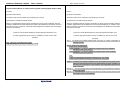
RENESAS TECHNICAL UPDATE
1753, Shimonumabe, Nakahara-ku, Kawasaki-shi, Kanagawa 211-8668 Japan
Renesas Electronics Corporation
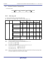
Product
Category
Title
MPU/MCU
Document
No.
TN-RL*-A004C/E
Correction for Incorrect Description Notice RL78/G14
Descriptions in the User’s Manual: Hardware Rev. 1.00
Changed
Information
Category
Technical Notification
Reference
Document
RL78/G14 User’s Manual: Hardware
Rev.1.00
R01UH0186EJ0100 (Dec. 2011)
Rev.
3.00
Lot No.
Applicable
Product
RL78/G14 Group
R5F104xxx
All lots
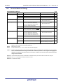
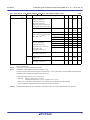
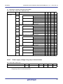
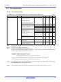
This document describes misstatements found in the RL78 User’s Manual: Hardware Rev.1.00 (R01UH0186EJ0100).
Corrections
Applicable Item
Applicable Page
Incorrect descriptions of reset processing time/standby mode
release time
Pages 1049, 1052 to
1055, 1060, 1061,
1072, 1073
Contents
Incorrect descriptions revised
27.3.6 Invalid memory access detection function
Page 1105
Incorrect descriptions revised
Cautions of flash memory programming by self-programming
Page 1142
Incorrect descriptions revised
Document Improvement
The above corrections will be made for the next revision of the User’s Manual: Hardware.
(c) 2013. Renesas Electronics Corporation. All rights reserved.
Page 1 of 50
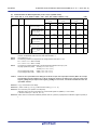
RENESAS TECHNICAL UPDATE TN-RL*-A004C/E
Date: October , 2013
Corrections in the User’s Manual: Hardware
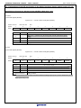
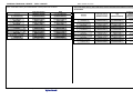
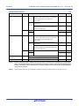
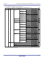
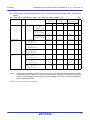
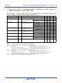
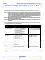
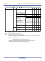
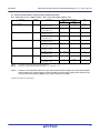
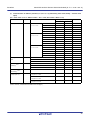
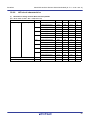
Corrections and Applicable Items
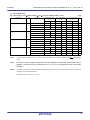
No.
1
2
3
4
5
6
7
8
9
10
11
12
13
14
15
16
17
18
19
20
21
22
23
24
25
26
27
28
29
30
31
32
33
34
35
36
Document No.
English
R01UH0186EJ0100
Specifications of the on-chip oscillator characteristics in the
Electrical specifications chapter
Incorrect descriptions of connection of unused pins of P60 to P63 in
Table 2-3 in the Pin functions chapter
Explanations of the timer RD status register
Explanations of the timer RD interrupt
Explanations of the timer RG status register
Explanations of the timer RG interrupt
Descriptions in the comparator block diagram
Cautions of the high-speed on-chip oscillator frequency select
register (HOCODIV)
Incorrect descriptions of reset processing time/standby mode
release time
Cautions of A/D converter mode register 0 (ADM0)
Incorrect descriptions of caution on A/D conversion time selection
Explanations when using SNOOZE mode in the A/D converter
chapter
Explanations when using temperature sensor and internal reference
voltage (1.45 V) of the A/D test function in the Safety functions
chapter
Cautions when using SNOOZE mode in the serial array unit
Explanations of the power-on-reset circuit
Explanations of the A/D test function in the Safety functions chapter
Explanations of the data flash in the Flash memory chapter
Cautions of flash memory programming by self-programming
Items of flash memory programming characteristics
3.1.3 Internal data memory space
17. 7. 3 SNOOZE mode function
23.2.2 STOP mode
23.2.3 SNOOZE mode
27.3.6 Invalid memory access detection function
Figure 29-3 Format of Option Byte (000C2H/010C2H)
34.4.1 Pin characteristics
34.4.2 Supply current characteristics
34.5 AC characteristics
34.6.1 Serial array unit
34.6.2 Serial interface IICA
34.7.1 A/D converter characteristics
34.7.2 Temperature Sensor/Internal Reference Voltage
Characteristics
34.7.5 POR circuit characteristics
Supply Voltage Rise Time
34.9 Data Memory STOP Mode Low Supply Voltage Data Retention
Characteristics
Chapter 30 ELECTRICAL SPECIFICATIONS (G:TA = −40 to
+105°C)
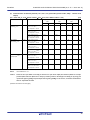
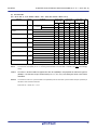
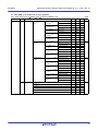
37
Incorrect descriptions of reset processing time/standby mode
release time
38
39
27.3.6 Invalid memory access detection function
Cautions of flash memory programming by self-programming
Page 1179
Page 4
Page 83
Page 5
Pages 470, 472
Page 518
Page 534
Page 562
Page 675
Pages 6 to 8
Pages 9 , 10
Pages 11, 12
Pages 13, 14
Pages 15, 16
Page 284
Page 17
Pages 1048 to 1050,
1052 to, 1055, 1060,
1061, 1072, 1073
Page 613
Pages 616 to 623
Pages 625, 626, and
658
Page 18
Page 19
Page 20
Pages 21 to 23
Pages 655, 662
Pages 24, 25
Pages 786, 788
Pages 1070, 1071
Page 1109
Page 1133
Page 1142
Page 1231
Page 105
Page 847
Pages 1050, 1052
Page 1055
Page 1105
Page 1121
Page 1181, 1182
Pages 1186 to 1195
Pages 1196 to 1197
Pages 1198 to 1221
Page 1222
Pages 1223 to 1226
Page 26
Page 27
Page 28
Page 29
Page 29
Page 30
Page 31
Pages 32, 33
Page 34
Page 34
Page 34
Page 35
Page 36
Page 36
Page 36
Page 36
Page 36
Page 36
Page 1227
Page 36
Page 1128
None
Page 36
Page 37
Page 1231
Page 37
None
Page 37
Pages 1049, 1052 to
1055, 1060, 1061,
1072, 1073
Page 1105
Page 1142
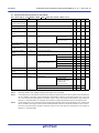
Incorrect: Bold with underline; Correct: Gray hatched
(c) 2013. Renesas Electronics Corporation. All rights reserved.
Pages in this
document for
corrections
Page 2 of 50
Pages 38 to 47
Pages 48, 49
Page 50
RENESAS TECHNICAL UPDATE TN-RL*-A004C/E
Date: October , 2013
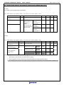
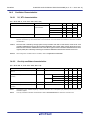
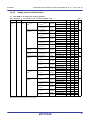
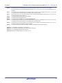
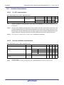
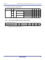
Revision History
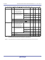
RL78/G14 Incorrect description notice, issued document history
Document Number
Issue Date
TN-RL*-A004A/E
Dec. 6, 2012
TN-RL*-A004B/E
July 4, 2013
TN-RL*-A004C/E
Oct. , 2013
(c) 2013. Renesas Electronics Corporation. All rights reserved.
Description
First edition issued
Incorrect descriptions of No.1 to No.19 revised
Rev. 2.00 issued
Revisions of No.20 to No.36 incorrect descriptions added
Rev. 3.00 issued
Incorrect descriptions of No.37 to No.39 revised (This notification)
Page 3 of 50
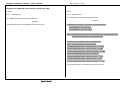
RENESAS TECHNICAL UPDATE TN-RL*-A004C/E
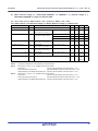
1.
Date: October , 2013
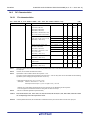
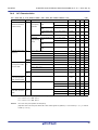
Specifications of the on-chip oscillator characteristics in the Electrical specifications
chapter fixed (page 1179)
Incorrect:
34.3.2 On-chip oscillator characteristics
(TA = −40 to +85°C, 1.6 V ≤ EVDD0 = EVDD1 ≤ VDD ≤ 5.5 V, VSS = EVSS0 = EVSS1 = 0 V)
Oscillators
Parameters
High-speed on-chip oscillator
clock frequency
Conditions
MIN.
MAX.
Unit
1
32
MHz
1.8 V VDD 5.5 V
−1
+1
%
1.6 V VDD < 1.8 V
−5
+5
%
1.8 V VDD 5.5 V
−1.5
+1.5
%
1.6 V VDD < 1.8 V
−5.5
+5.5
%
fIH
TYP.
Note 1
High-speed on-chip oscillator
clock frequency accuracy
−20 to +85C
Note 2
−40 to −20C
Low-speed on-chip oscillator
fIL
15
kHz
clock frequency
Low-speed on-chip oscillator
−15
+15
%
clock frequency accuracy
Notes
1. High-speed on-chip oscillator frequency is selected with bits 0 to 4 of the option byte (000C2H/010C2H) and bits
0 to 2 of the HOCODIV register.
2. This only indicates the oscillator characteristics. Refer to AC Characteristics for instruction execution time.
When SSOP (30-pin), WQFN (32-, 40-, 48-pin), FLGA (36-pin), LQFP (7 7) (48-pin), LQFP (10 10) (52-pin),
LQFP (12 12) (64-, 80-pin), LQFP (14 14) (80-, 100-pin), LQFP (14 20) (100-pin) products, these
specifications show target values, which may change after device evaluation.
Correct:
34.3.2 On-chip oscillator characteristics
(TA = −40 to +85°C, 1.6 V ≤ EVDD0 = EVDD1 ≤ VDD ≤ 5.5 V, VSS = EVSS0 = EVSS1 = 0 V)
Oscillators
Parameters
High-speed on-chip oscillator
clock frequency
Conditions
MIN.
MAX.
Unit
1
32
MHz
1.8 V VDD 5.5 V
−1
+1
%
1.6 V VDD < 1.8 V
−5
+5
%
1.8 V VDD 5.5 V
−1.5
+1.5
%
1.6 V VDD < 1.8 V
−5.5
+5.5
%
fIH
TYP.
Note 1
High-speed on-chip oscillator
clock frequency accuracy
−20 to +85C
Note 2
−40 to −20C
Low-speed on-chip oscillator
fIL
15
kHz
clock frequency
Low-speed on-chip oscillator
−15
+15
%
clock frequency accuracy
Notes
1. High-speed on-chip oscillator frequency is selected with bits 0 to 4 of the option byte (000C2H/010C2H) and bits
0 to 2 in the HOCODIV register.
2. This table only indicates the oscillator characteristics.
(c) 2013. Renesas Electronics Corporation. All rights reserved.
Refer to AC Characteristics for instruction execution time.
Page 4 of 50
RENESAS TECHNICAL UPDATE TN-RL*-A004C/E
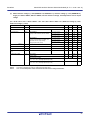
2.
Date: October , 2013
Incorrect descriptions of connection of unused pins of P60 to P63 in Table 2-3 in the Pin
functions chapter revised (page 83)
Incorrect:
Table 2-3. Connection of Unused Pins (100-pin products) (2/3)
Pin Name
I/O Circuit Type
I/O
Recommended Connection of Unused Pins
(Omitted)
P60/SCLA0
13-R
I/O
Input:
Independently connect to EVDD0, EVDD1 or EVSS0, EVSS1
via a resistor.
P61/SDAA0
Output: Leave open.
P62/SCLA1
P63/SDAA1
P64/TI10/TO10
8-R
P65/TI11/TO11
P66/TI12/TO12
P67/TI13/TO13
(Omitted)
Correct:
Table 2-3. Connection of Unused Pins (100-pin products) (2/3)
Pin Name
I/O Circuit Type
I/O
Recommended Connection of Unused Pins
(Omitted)
P60/SCLA0
13-R
I/O
Input:
Connect these pins independently to EVDD0, EVDD1 or
EVSS0, EVSS1 via a resistor.
P61/SDAA0
Output: Set 0 to the port output latch when using these pins left
P62/SCLA1
open. Set 1 to the port output latch when connecting
P63/SDAA1
these pins independently to EVDD0, EVDD1, or EVSS0,
EVSS1 via a resistor.
P64/TI10/TO10
8-R
P65/TI11/TO11
P66/TI12/TO12
Input:
Connect these pins independently to EVDD0, EVDD1 or
EVSS0, EVSS1 via a resistor.
Output: Leave open.
P67/TI13/TO13
(Omitted)
(c) 2013. Renesas Electronics Corporation. All rights reserved.
Page 5 of 50
RENESAS TECHNICAL UPDATE TN-RL*-A004C/E
3.
Date: October , 2013
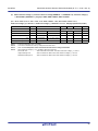
Explanations of the timer RD status register added
Explanations of the timer RD status register added (pages 470, 472)
Incorrect:
Notes
1. The value after reset is undefined when FRQSEL4 = 1 in the user option byte (000C2H/010C2H) and TRD0EN = 0
in the PER1 register. If it is necessary to read the initial value, set fCLK to fIH and TRD0EN = 1 before reading.
(Omitted)
4. The writing results are as follows:
If the read value is 1, writing 0 to the bit sets it to 0.
If the read value is 0, the bit remains unchanged even if 0 is written to it. (Even if the bit is changed from 0 to 1
after reading and then 0 is written to it, it remains 1.)
Writing 1 has no effect.
(c) 2013. Renesas Electronics Corporation. All rights reserved.
Page 6 of 50
RENESAS TECHNICAL UPDATE TN-RL*-A004C/E
Date: October , 2013
Correct:
Notes 1. The value after reset is undefined when FRQSEL4 = 1 in the user option byte (000C2H/010C2H) and TRD0EN = 0 in
the PER1 register. If it is necessary to read the initial value, set fCLK to fIH and TRD0EN = 1 before reading.
(Omitted)
4. The writing results are as follows:
Writing 1 has no effect.
If the read value is 0, the bit remains unchanged even if 0 is written to it. (Even if the bit is changed from 0 to 1
after reading and then 0 is written to it, it remains 1.)
If the read value is 1, writing 0 to the bit sets it to 0. When status flags of interrupt sources (applicable status flags)
of timer RD are set to 0 and their interrupts are disabled in timer RD interrupt enable
register i (TRDIERi), use either one of the following methods (a) to (c).
(a)
Set 00H (all interrupts disabled) to timer RD interrupt enable register i (TRDIERi) and write 0 to applicable
status flags.
(b)
When there are bits set to 1 (interrupt-enabled) in timer RD interrupt enable register i (TRDIERi) and status
flags of interrupt sources related to their bits are 0, write 0 to applicable status flags.
Example: To clear the IMFB bit to 0 when bits IMIEA and OVIE are set to 1 (interrupt-enabled) and the IMIEB
bit is set to 0 (interrupt-disabled).
Timer RD Interrupt Enable Register i (TRDIERi)
Interrupt-enabled
TRDIERi
–
0
–
0
–
0
OVIE
1
IMIED
0
IMIEC
0
IMIEB
0
IMIEA
1
Interrupt-disabled
Timer RD Status Register i (TRDSRi)
Bit to be cleared to 0
TRDSRi
–
0
–
0
UDF
0
OVF
0
IMFD
1
IMFC
0
As status flags (OVF, IMFA) corresponding to the bit which is set
to 1 (interrupt-enabled) are 0, write 0 to the IMFB bit.
(Go on to the next page)
(c) 2013. Renesas Electronics Corporation. All rights reserved.
Page 7 of 50
IMFB
1
IMFA
0
RENESAS TECHNICAL UPDATE TN-RL*-A004C/E
(c)
Date: October , 2013
When there are bits set to 1 (interrupt-enabled) in timer RD interrupt enable register i (TRDIERi) and status
flags of interrupt sources related to their bits are 1, write 0 to these status flags and applicable status flags
at the same time.
Example: To clear the IMFB bit to 0 when the IMIEA bit is set to 1 (interrupt-enabled) and the IMIEB bit is set
to 0 (interrupt-disabled).
Timer RD Interrupt Enable Register i (TRDIERi)
Interrupt-enabled
TRDIERi
–
0
–
0
–
0
OVIE
1
IMIED
0
IMIEC
0
IMIEB
0
IMIEA
1
Interrupt-disabled
Timer RD Status Register i (TRDSRi)
Bit to be cleared to 0
TRDSRi
–
0
–
0
UDF
0
OVF
0
IMFD
1
IMFC
0
As the status flag (IMFA) corresponding to the bit which is set to
1 (interrupt-enabled) is 1, write 0 to bits IMFB and IFMA at the
same time.
(c) 2013. Renesas Electronics Corporation. All rights reserved.
Page 8 of 50
IMFB
1
IMFA
1
RENESAS TECHNICAL UPDATE TN-RL*-A004C/E
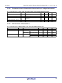
4.
Date: October , 2013
Explanations of the timer RD interrupt added
Explanations of the timer RD interrupt added (page 518)
Incorrect:
Since the interrupt source (timer RD interrupt) is generated by a combination of multiple interrupt request sources for timer RD,
the following differences from other maskable interrupts apply:
(Omitted)
While multiple bits in the TRDIERi register are set to 1, if the first request source is met and the TRDIFi bit is set to 1, and
then the next request source is met, the TRDIFi bit is cleared to 0 when the interrupt is acknowledged. However, if the
previously met request source is cleared, the TRDIFi bit is set to 1 by the next generated request source.
Correct:
Since the interrupt source (timer RD interrupt) is generated by a combination of multiple interrupt request sources for timer RD,
the following differences from other maskable interrupts excluding the timer RG interrupt apply:
(Omitted)
While multiple bits in the TRDIERi register are set to 1, if the first request source is met and the TRDIFi bit is set to 1, and
then the next request source is met, the TRDIFi bit is cleared to 0 when the interrupt is acknowledged. However, if the
previously-met request source is cleared, the TRDIFi bit is set to 1 by the next generated request source.
When status flags of interrupt sources (applicable status flags) of the timer RD are set to 0 and their interrupts are disabled
in timer RD interrupt enable register i (TRDIERi), use either one of the following methods (a) to (c).
(a)
Set 00H (all interrupts disabled) to timer RD interrupt enable register i (TRDIERi) and write 0 to applicable status flags.
(b)
When there are bits set to 1 (enabled) in timer RD interrupt enable register i (TRDIERi) and status flags of interrupt
sources related to their bits are 0, write 0 to applicable status flags.
Example: To clear the IMFB bit to 0 when bits IMIEA and OVIE are set to 1 (interrupt-enabled) and the IMIEB bit is set
to 0 (interrupt-disabled).
Timer RD Interrupt Enable Register i (TRDIERi)
Interrupt-enabled
TRDIERi
–
0
–
0
–
0
OVIE
1
IMIED
0
IMIEC
0
IMIEB
0
IMIEA
1
Interrupt-disabled
Timer RD Status Register i (TRDSRi)
Bit to be cleared to 0
TRDSRi
–
0
–
0
UDF
0
OVF
0
IMFD
1
IMFC
0
As status flags (OVF, IMFA) corresponding to the bit which
is set to 1 (interrupt-enabled) are 0, write 0 to the IMFB bit.
(Go on to the next page)
(c) 2013. Renesas Electronics Corporation. All rights reserved.
Page 9 of 50
IMFB
1
IMFA
0
RENESAS TECHNICAL UPDATE TN-RL*-A004C/E
(c)
Date: October , 2013
When there are bits set to 1 (interrupt-enabled) in timer RD interrupt enable register i (TRDIERi) and status flags of
interrupt sources related to their bits are 1, write 0 to these status flags and applicable status flags at the same time.
Example: To clear the IMFB bit to 0 when the IMIEA is set to 1 (interrupt-enabled) and the IMIEB is set to 0
(interrupt-disabled).
Timer RD Interrupt Enable Register i (TRDIERi)
Interrupt-enabled
TRDIERi
–
0
–
0
–
0
OVIE
1
IMIED
0
IMIEC
0
IMIEB
0
IMIEA
1
Interrupt-disabled
Timer RD Status Register i (TRDSRi)
Bit to be cleared to 0
TRDSRi
–
0
–
0
UDF
0
OVF
0
IMFD
1
IMFC
0
As the status flag (IMFA) corresponding to the bit which is set to 1
(interrupt-enabled) is 1, write 0 to bits IMFB and IMFA at the same time.
(c) 2013. Renesas Electronics Corporation. All rights reserved.
Page 10 of 50
IMFB
1
IMFA
1
RENESAS TECHNICAL UPDATE TN-RL*-A004C/E
5.
Date: October , 2013
Explanations of the timer RG status register added
Explanations of the timer RG status register added (page 534)
Incorrect:
Note 1.
When the counter value of timer RG changes from FFFFH to 0000H, the TRGOVF bit is set to 1.
(Omitted)
Note 2.
The writing results are as follows:
If the read value is 1, writing 0 to the bit sets it to 0.
If the read value is 0, the bit remains unchanged even if 0 is written to it. (Even if the bit is changed from 0 to 1.)
After reading and then 0 is written to it, it remains 1.
Writing 1 has no effect.
Correct:
Note 1.
When the counter value of timer RG changes from FFFFH to 0000H, the TRGOVF bit is set to 1.
(Omitted)
Note 2.
The writing results are as follows:
Writing 1 has no effect.
If the read value is 0, the bit remains unchanged even if 0 is written to it. (Even if the bit is changed from 0 to 1.)
If the read value is 1, writing 0 to the bit sets it to 0. When status flags of interrupt sources (applicable status flags)
of the timer RG are set to 0 and their interrupts are disabled in the timer RG interrupt enable register (TRGIER), use
either one of the following methods (a) to (c).
(a) Set 00H (all interrupts disabled) to timer RG interrupt enable register (TRGIER) and write 0 to applicable status
flags.
(Go on to the next page)
(c) 2013. Renesas Electronics Corporation. All rights reserved.
Page 11 of 50
RENESAS TECHNICAL UPDATE TN-RL*-A004C/E
Date: October , 2013
(b) When there are bits set to 1 (interrupt-enabled) in timer RG interrupt enable register (TRGIER) and status flags of
interrupt sources related to their bits are 0, write 0 to applicable status flags.
Example: To clear the TRGIMFB bit to 0 when bits TRGIMIEA and TRGOVIE are set to 1 (interrupt-enabled) and
the TRGIMIEB bit is set to 0 (interrupt-disabled)
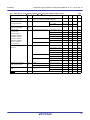
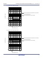
Timer RG Interrupt Enable Register (TRGIER)
Interrupt-enabled
TRGIER
–
0
–
0
–
0
–
0
TRGOVIE
1
TRGUDIE
0
TRGIMIEB
0
TRGIMIEA
1
Interrupt-disabled
Timer RG Status Register (TRGSR)
TRGSR
–
0
–
0
–
0
TRGDIRF
0
TRGOVF
0
Bit to be cleared to 0
TRGUDF
1
TRGIMFB
1
TRGIMFA
0
As status flags (TRGOVF, TRGIMFA) corresponding to the bit
which is set to 1 (interrupt-enabled), write 0 to the TRGIMFB
bit.
(c) When there are bits set to 1 (interrupt-enabled) in timer RG interrupt enable register (TRGIER) and status flags of
interrupt sources related to their bits are 1, write 0 to these status flags and applicable status flags at the same
time.
Example: To clear the TRGIMFB bit to 0 when the TRGIMIEA bit is set to 1 (interrupt-enabled) and the TRGIMIEB
bit is set to 0 (interrupt-disabled).
Timer RG Interrupt Enable Register (TRGIER)
TRGIER
–
0
–
0
–
0
–
0
TRGOVIE
0
Interrupt-enabled
TRGUDIE
0
TRGIMIEB
0
TRGIMIEA
1
Interrupt-disabled
Timer RG Status Register (TRGSR)
TRGSR
–
0
–
0
–
0
TRGDIRF
0
TRGOVF
0
Bit to be cleared to 0
TRGUDF
1
As the status flag (TRGIMFA) corresponding to the bit which is
set to 1 (interrupt-enabled) is 1, write 0 to bits TRGIMFB and
TRGIFMA at the same time.
(c) 2013. Renesas Electronics Corporation. All rights reserved.
Page 12 of 50
TRGIMFB
1
TRGIMFA
1
RENESAS TECHNICAL UPDATE TN-RL*-A004C/E
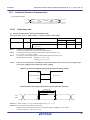
6.
Date: October , 2013
Explanations of the timer RG interrupt added
Explanations of the timer RG interrupt added (Page 562)
Incorrect: Not applicable (new)
Correct:
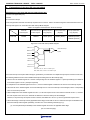
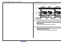
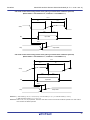
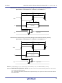
9.4 Timer RG Interrupt
Timer RG generates the timer RG interrupt request from four sources. Table 9-16 lists the Registers Associated with Timer RG
Interrupt and Figure 9-31 shows the Timer RG Interrupt Block Diagram.
Table 9-16 Registers Associated with Timer RG Interrupt
Timer RG
Timer RG
Timer RG Interrupt
Interrupt Request
Interrupt Mask Flag
Priority Specification
Status Register
Enable Register
Flag (Register)
(Register)
Flag (Register)
TRGSR
TRGIER
TRGIF (IF2H)
TRGMK (MK2H)
TRGPR0 (PR02H)
TRGPR1 (PR12H)
Figure 9-31 Timer RG Interrupt Block Diagram
IMFA bit
Timer RG interrupt
IMIEA bit
request
IMFB bit
IMIEB bit
UDF bit
UDIE bit
OVF bit
OVIE bit
IMFA, IMFB, UDF, OVF: Bits in the TRGSR register
IMIEA, IMIEB, UDIE, OVIE: Bits in the TRGIER register
Since the interrupt source (timer RG interrupt) is generated by a combination of multiple interrupt request sources for timer RG,
the following differences from other maskable interrupts excluding the timer RD interrupt apply:
When a bit in the TRGSR register is 1 and the corresponding bit in the TRGIER register is 1 (interrupt-enabled), the TRGIF bit
in the IF2H register is set to 1 (interrupt requested).
If multiple bits in the TRGIER register are set to 1, use the TRGSR register to determine the source of the interrupt request.
Since the bits in the TRGSR register are not automatically set to 0 even if the interrupt is acknowledged, set the corresponding
bit to 0 in the interrupt routine.
While multiple bits in the TRGIER register are set to 1, if the first request source is met and the TRGIF bit is set to 1, and then
the next request source is met, the TRGIF bit is cleared to 0 when the interrupt is acknowledged.
However, if the previously-met request source is cleared, the TRGIF bit is set to 1 by the next generated request source.
When status flags of interrupt sources (applicable status flags) of timer RG are set to 0 and their interrupts are disabled in the
timer RG interrupt enable register (TRGIER), use either one of the following methods (a) to (c).
(a) Set 00H (all interrupts disabled) to the TRGIER register and write 0 to applicable status flags.
(Go on to the next page)
(c) 2013. Renesas Electronics Corporation. All rights reserved.
Page 13 of 50
RENESAS TECHNICAL UPDATE TN-RL*-A004C/E
Date: October , 2013
(b) When there are bits set to 1 (interrupt-enabled) in timer RG interrupt enable register (TRGIER) and status flags of
interrupt sources related to their bits are 0, write 0 to applicable status flags.
Example: To clear the TRGIMFB bit to 0 when bits TRGIMIEA and TRGOVIE are set to 1 (interrupt-enabled) and the
TRGIMIEB bit is set to 0 (interrupt-disabled).
Timer RG Interrupt Enable Register (TRGIER)
Interrupt-enabled
TRGIER
–
0
–
0
–
0
–
0
TRGOVIE
1
TRGUDIE
0
TRGIMIEB
0
TRGIMIEA
1
Interrupt-disabled
Timer RG Status Register (TRGSR)
TRGSR
–
0
–
0
–
0
TRGDIRF
0
TRGOVF
0
Bit to be cleared to 0
TRGUDF
1
TRGIMFB
1
TRGIMFA
0
As status flags (TRGOVF, TRGIMFA) corresponding to
the bit which is set to 1 (interrupt-enabled) are 0, write 0
to the TRGIMFB bit.
(c) When there are bits set to 1 (interrupt-enabled) in the timer RG interrupt enable register (TRGIER) and status flags
of interrupt sources related to their bits are 1, write 0 to these status flags and applicable status flags at the same
time.
Example: To clear the TRGIMFB bit to 0 when the TRGIMIEA bit is set to 1 (interrupt-enabled) and the TRGIMIEB bit
is set to 0 (interrupt-disabled).
Timer RG Interrupt Enable Register (TRGIER)
TRGIER
–
0
–
0
–
0
–
0
TRGOVIE
0
Interrupt-enabled
TRGUDIE
0
TRGIMIEB
0
TRGIMIEA
1
Interrupt-disabled
Timer RG Status Register (TRGSR)
TRGSR
–
0
–
0
–
0
TRGDIRF
0
TRGOVF
0
Bit to be cleared to 0
TRGUDF
1
As the status flag (TRGIMFA) corresponding to the bit which is
set to 1 (interrupt-enabled) is 1, write 0 to bits TRGIMFB and
TRGIFMA at the same time.
(c) 2013. Renesas Electronics Corporation. All rights reserved.
Page 14 of 50
TRGIMFB
1
TRGIMFA
1
RENESAS TECHNICAL UPDATE TN-RL*-A004C/E
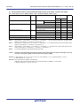
7.
Date: October , 2013
Descriptions in the comparator block diagram improved
Descriptions in the comparator block diagram improved (page 675)
Incorrect:
Figure 16-1 Comparator Block Diagram
Digital filter
(match
3 times)
C1WDE
IVCMP1
IVREF1
Internal reference
voltage (1.45 V)
C1VRF
=0
-
= 00B
One-edge
detection
=1
=0
C1IE
C1OP = 1
C1MON
C1EDG
=0
C1OE
C0OP = 0
C0OE
SPDMD
C0VRF
=1
IVREF0
C1EPO = 0
C1FCK1 C1FCK0
= other than
=1
00B
+
=1
Both-edge
detection
=0
IVCMP0
-
C0MON
C0FCK1 C0FCK0
= 00B
+
Digital filter
(match
3 times)
C0WDE
fCLK /32 = 11B
fCLK /8 = 10B
fCLK = 01B
=1
= other than C0EPO = 1
00B
=0
C0IE
One-edge
detection
Both-edge
detection
COMP1
ELC event
COMP1
interrupt
I/O control
C1FCK1 - C1FCK0
fCLK = 01B
Sampling clock
fCLK /8 = 10B
=
11B
fCLK /32
C0EDG
=0
=1
COMP0
interrupt
COMP0
ELC event
Sampling clock
C1FCK1 - C1FCK0
Remarks: C1MON, C0MON, C1VRF, C0VRF, C1WDE, C0WDE: Bits in the COMPMDR register
C1FCK1, C1FCK0, C0FCK1, C0FCK0, C1EDG, C0EDG, C1EPO, C0EPO: Bits in the COMPFIR register
SPDMD, C1PO, C0PO, C1OE, C0OE, C1IE, C0IE: Bits in the COMPOCR register
(c) 2013. Renesas Electronics Corporation. All rights reserved.
Page 15 of 50
VCOUT1
VCOUT0
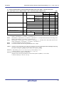
RENESAS TECHNICAL UPDATE TN-RL*-A004C/E
Date: October , 2013
Correct:
Figure 16-1 Comparator Block Diagram
Comparator 0
C0FCK1 - C0FCK0
fCLK = 01B
= 10B
fCLK/8 = 11B
fCLK/32
Sampling clock
Digital filter
(match
3 times)
C0ENB
C0FCK1 - C0FCK0
= other than 00B
C0EPO
=0
IVCMP0
One-edge
detection
C0EDG
=1
=0
= 00B
C0IE
=1
COMP0
ELC event
=1
C0VRF
= 0 C0WDE
=0
INTCMP0
(comparator detection 0 interrupt)
C0MON
=1
C0OP
=1
I/O control
IVREF0
Both-edge
detection
= 0 C0OE
VCOUT0
C0ENB
C0WDE
IVCMP1
Comparator 1
I/O control
IVREF1
COMP1
ELC event
INTCMP1
(comparator detection 1 interrupt)
VCOUT1
Internal reference
voltage (1.45 V)
SPDMD
VTW+
VTW-
Note
Note:
When setting either the C0WDE bit or C1WDE bit, or both bits to 1, this switch is turned ON, and the division resistor to generate
the comparison voltage becomes enabled.
Remarks:
n = 0, 1
CnMON, CnVRF, CnWDE, CnENB: Bits in the COMPMDR register
CnFCK1, CnFCK0, CnEDG, CnEPO: Bits in the COMPFIR register
SPDMD, CnOP, CnOE, CnIE: Bits in the COMPOCR register
(c) 2013. Renesas Electronics Corporation. All rights reserved.
Page 16 of 50
RENESAS TECHNICAL UPDATE TN-RL*-A004C/E
8.
Date: October , 2013
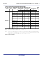
Cautions of the high-speed on-chip oscillator frequency select register (HOCODIV) revised
(page 284)
Incorrect:
(8) High-speed on-chip oscillator frequency select register (HOCODIV)
(Omitted)
Caution 1. Set the HOCODIV register within the operable voltage range both before and after changing the frequency.
Caution 2. Use the device within the voltage of the flash operation mode set by the option byte (000C2H/010C2H) even
after the frequency has been changed by using the HOCODIV register.
Option Byte
Flash Operation Mode
(000C2H/010C2H) Value
Operating Frequency
Operating Voltage
Range
Range
CMODE1
CMODE2
0
0
LV (low-voltage main) mode
1 to 4 MHz
1.6 to 5.5 V
1
0
LS (low-speed main) mode
1 to 8 MHz
1.8 to 5.5 V
1
1
HS (high-speed main) mode
1 to 16 MHz
2.4 to 5.5 V
1 to 32 MHz
2.7 to 5.5 V
Caution 3. When setting of high-speed on-chip oscillator clock as system clock, the device operates at the old
frequency for the duration of 3 clocks after the frequency value has been changed by using the HOCODIV
register.
Caution 4. To change the frequency of the high-speed on-chip oscillator when X1 oscillation, external oscillation
input or subclock is set for the system clock, stop the high-speed on-chip oscillator by setting bit 0
(HIOSTOP) of the CSC register to 1 and the change the frequency.
Correct:
(8) High-speed on-chip oscillator frequency select register (HOCODIV)
(Omitted)
Caution 1. When changing the frequency of the high-speed on-chip oscillator by the HOCODIV register, make sure
the previously-set frequency and newly-set frequency fall within the operating frequency range for the flash
operation mode set by the option byte (000C2H).
Option Byte
Flash Operation Mode
(000C2H) Value
Operating Frequency
Operating Voltage
Range
Range
CMODE1
CMODE2
0
0
LV (low-voltage main) mode
1 to 4 MHz
1.6 to 5.5 V
1
0
LS (low-speed main) mode
1 to 8 MHz
1.8 to 5.5 V
1
1
HS (high-speed main) mode
1 to 16 MHz
2.4 to 5.5 V
1 to 32 MHz
2.7 to 5.5 V
2. Set the HOCODIV register while the high-speed on-chip oscillator clock (fIH) is selected as the CPU/peripheral
hardware clock (fCLK).
3. After the frequency has been changed using the HOCODIV register and the following transition time has been
elapsed, the frequency is switched.
• The device operates at the frequency for the duration of 3 clocks before the frequency has been changed.
• The CPU/peripheral hardware clock waits for maximum 3 clocks at the frequency after the frequency has been
changed.
(c) 2013. Renesas Electronics Corporation. All rights reserved.
Page 17 of 50
RENESAS TECHNICAL UPDATE TN-RL*-A004C/E
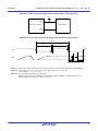
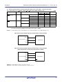
9.
Date: October , 2013
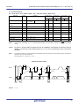
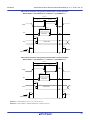
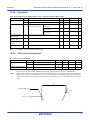
Incorrect descriptions of reset processing time/standby mode release time revised
Incorrect descriptions of HALT mode release time revised (page 1048)
Incorrect:
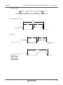
Figure 23-3 HALT Mode Release by Interrupt Request Generation
HALT
instruction
Interrupt
request
Standby
release signal
Status of CPU
Operating mode
Wait Note
HALT mode
Oscillation
High-speed system clock,
High-speed on-chip oscillator clock,
or subsystem clock
Note
Operating mode
Wait time for HALT mode release
When vectored interrupt servicing is carried out
Main system clock: 13 to 15 clock
Subsystem clock (RTCLPC = 0): 8 to 10 clock
Subsystem clock (RTCLPC = 1): 9 to 11 clock
When vectored interrupt servicing is not carried out
Main system clock: 8 to 9 clock
Subsystem clock (RTCLPC = 0): 3 to 4 clock
Subsystem clock (RTCLPC = 1): 4 to 5 clock
Correct:
Figure 23-3 HALT Mode Release by Interrupt Request Generation
HALT
instruction
Interrupt
request
Standby release signal Note 1
Status of CPU
Operating mode
High-speed system clock,
High-speed on-chip oscillator clock,
or subsystem clock
Wait Note 2
HALT mode
Operating mode
Oscillation
Notes 1. For details of the standby release signal, see Figure 21-1
2. Wait time for HALT mode release
When vectored interrupt servicing is carried out
Main system clock: 15 to 16 clocks
Subsystem clock (RTCLPC = 0): 10 to 11 clocks
Subsystem clock (RTCLPC = 1): 11 to 12 clocks
When vectored interrupt servicing is not carried out
Main system clock: 9 to 10 clocks
Subsystem clock (RTCLPC = 0): 4 to 5 clocks
Subsystem clock (RTCLPC = 1): 5 to 6 clocks
For details about incorrect descriptions in pages 1049, 1050, 1052 to 1055, 1060, 1061, 1072, and 1073, refer to No.37 (pages
38 to 47) in this document.
(c) 2013. Renesas Electronics Corporation. All rights reserved.
Page 18 of 50
RENESAS TECHNICAL UPDATE TN-RL*-A004C/E
Date: October , 2013
10. Cautions of A/D converter mode register 0 (ADM0) added (page 613)
Incorrect:
(2) A/D converter mode register 0 (ADM0)
(Omitted)
Notes 1. For details of the FR2 to FR0, LV1, LV0 bits, and A/D conversion, see Table 14-3 A/D Conversion Time Selection.
2. While in the software trigger mode or hardware trigger wait mode, the ADCS bit can be used as a status flag
for the conversion operation status. However, while in the hardware trigger no-wait mode, this bit cannot be
used as a status flag.
3. While in the software trigger mode or hardware trigger no-wait mode, the operation of the A/D voltage comparator is
controlled by the ADCS and ADCE bits, and it takes 1 µs from the start of operation for the operation to stabilize.
Therefore, when the ADCS bit is set to 1 after 1 µs or more has elapsed from the time ADCE bit is set to 1, the
conversion result at that time has priority over the first conversion result. Otherwise, ignore data of the first conversion.
Correct:
(2) A/D converter mode register (ADM0)
(Omitted)
Notes 1. For details of the FR2 to FR0, LV1, LV0 bits, and A/D conversion, see Table 14-3 A/D Conversion Time Selection.
(Deleted)
2. In software trigger mode or hardware trigger no-wait mode, the operation of the A/D voltage comparator is
controlled by bits ADCS and ADCE, and it takes 1 µs from the start of operation for the operation to stabilize.
Therefore, when the ADCS bit is set to 1 after 1 µs or more has elapsed from the time ADCE bit is set to 1, the
conversion result at that time has priority over the first conversion result. Otherwise, ignore data of the first conversion.
Cautions 1. Change bits ADMD, FR2 to FR0, LV1, and LV0 while conversion is stopped (ADCS = 0, ADCE = 0).
2. Do not set the ADCS bit to 1 and the ADCE bit to 0 at the same time.
3. Do not change bits ADCS and ADCE from 0 to 1 at the same time using an 8-bit manipulation instruction.
Make sure to set these bits in the order shown in 14.7 A/D Converter Setup Flowchart.
(c) 2013. Renesas Electronics Corporation. All rights reserved.
Page 19 of 50
RENESAS TECHNICAL UPDATE TN-RL*-A004C/E
Date: October , 2013
11. Incorrect descriptions of caution on A/D conversion time selection revised (pages 616 to 623)
Incorrect:
Table 14-3 A/D Conversion Time Selection
(Omitted)
Cautions 1. When rewriting the FR2 to FR0, LV1, and LV0 bits to other than the same data, stop A/D conversion once
(ADCS = 0) beforehand.
Correct:
Table 14-3 A/D Conversion Time Selection
(Omitted)
Cautions 1. Rewrite bits FR2 to FR0, LV1, and LV0 to other than the same data while conversion is stopped (ADCS = 0,
ADCE = 0).
(c) 2013. Renesas Electronics Corporation. All rights reserved.
Page 20 of 50
RENESAS TECHNICAL UPDATE TN-RL*-A004C/E
Date: October , 2013
12. Explanations when using SNOOZE mode in the A/D converter chapter added
Explanations of A/D converter mode register 2 (ADM2) added (pages 625, 626)
Incorrect:
(4) A/D converter mode register 2 (ADM2)
(Omitted)
ADREFP1
ADREFP0
Selection of the + side reference voltage source of the A/D converter
0
0
Supplied from VDD
0
1
Supplied from P20/AVREFP/ANI0
1
0
Supplied from the internal reference voltage (1.45 V)
1
1
Setting prohibited
• When ADREFP1 or ADREFP0 bit is rewritten, this must be configured in accordance with the following procedures.
(1) Set ADCE = 0
(2) Change the values of ADREFP1 and ADREFP0
(3) Stabilization wait time (A)
(4) Set ADCE = 1
(5) Stabilization wait time (B)
When ADREFP1 and ADREFP0 are set to 1 and 0, the setting is changed to A = 1 µs, B = 5 µs.
When ADREFP1 and ADREFP0 are set to 0 and 0 or 0 and 1, A needs no wait and B = 1 µs.
• When ADREFP1 and ADREFP0 are set to 1 and 0, respectively, A/D conversion cannot be performed on the
temperature sensor output.
Be sure to perform A/D conversion while ADISS = 0.
AWC
Specification of the SNOOZE mode
0
Do not use the SNOOZE mode function.
1
Use the SNOOZE mode function.
When there is a hardware trigger signal in the STOP mode, the STOP mode is exited, and A/D conversion is performed
without operating the CPU (the SNOOZE mode).
The SNOOZE mode function can only be specified when the high-speed on-chip oscillator clock is selected for the
CPU/peripheral hardware clock (fCLK).
If any other clock is selected, specifying this mode is prohibited.
Using the SNOOZE mode function in the software trigger mode or hardware trigger no-wait mode is prohibited.
Using the SNOOZE mode function in the sequential conversion mode is prohibited.
When using the SNOOZE mode function, specify a hardware trigger interval of at least “A/D conversion time
with stabilization wait time” listed for Table 14-3.
(c) 2013. Renesas Electronics Corporation. All rights reserved.
Page 21 of 50
RENESAS TECHNICAL UPDATE TN-RL*-A004C/E
Date: October , 2013
Correct:
(4) A/D converter mode register 2 (ADM2)
(Omitted)
ADREFP1
ADREFP0
Selection of the + side reference voltage source of the A/D converter
0
0
Supplied from VDD
0
1
Supplied from P20/AVREFP/ANI0
1
0
Supplied from the internal reference voltage (1.45 V)
1
1
Setting prohibited
Note
When ADREFP1 or ADREFP0 bit is rewritten, this must be configured in accordance with the following procedures.
(1) Set ADCE = 0
(2) Change the values of ADREFP1 and ADREFP0
(3) Stabilization wait time (A)
(4) Set ADCE = 1
(5) Stabilization wait time (B)
When ADREFP1 and ADREFP0 are set to 1 and 0, respectively, the setting is changed to A = 5 µs, B = 1 µs.
When ADREFP1 and ADREFP0 are set to 0 and 0, respectively, or set to 0 and 1, respectively, A needs no wait and
B = 1 µs.
After (5) stabilization time, start the A/D conversion.
When ADREFP1 and ADREFP0 are set to 1 and 0, respectively, A/D conversion cannot be performed on the
temperature sensor output and internal reference voltage output.
Make sure to perform A/D conversion while ADISS = 0.
AWC
Specification of the SNOOZE mode
0
Do not use the SNOOZE mode function.
1
Use the SNOOZE mode function.
When there is a hardware trigger signal in the STOP mode, the STOP mode is exited, and A/D conversion is performed
without operating the CPU (the SNOOZE mode).
The SNOOZE mode function can only be specified when the high-speed on-chip oscillator clock is selected for the
CPU/peripheral hardware clock (fCLK). If any other clock is selected, specifying this mode is prohibited.
Using the SNOOZE mode function in the software trigger mode or hardware trigger no-wait mode is prohibited.
Using the SNOOZE mode function in the sequential conversion mode is prohibited.
When using the SNOOZE mode function, specify a hardware trigger interval of at least “shift time to SNOOZE mode
(Note)
+ A/D power supply stabilization wait time + A/D conversion time +2 fCLK clocks”
Even when using SNOOZE mode, make sure to set the AWC bit to 0 in normal operation mode and change it to 1
just before transiting to STOP mode.
Also, make sure to change the AWC bit to 0 after returning from STOP mode to normal operation mode.
If the AWC bit is left set to 1, A/D conversion will not start normally in spite of the subsequent SNOOZE or normal
operation mode.
Note
Refer to 23.2.3 SNOOZE mode.
(c) 2013. Renesas Electronics Corporation. All rights reserved.
Page 22 of 50
RENESAS TECHNICAL UPDATE TN-RL*-A004C/E
Date: October , 2013
Explanations of SNOOZE mode related to the A/D converter added (page 658)
Incorrect:
(1) If an interrupt is generated after A/D conversion ends
(Omitted)
While in the select mode
After A/D conversion ends and the A/D conversion end interrupt request signal (INTAD) is generated, the clock
request signal remains at the high level, and the A/D converter switches from the SNOOZE mode to the normal
operation mode.
To stop the high-speed on-chip oscillator clock supplied while in the SNOOZE mode, clear
bit 2 (AWC) of A/D converter mode register 2 (ADM2) to 0. Doing this sets the clock request signal (an internal
signal) to the low level and stops the supply of the high-speed on-chip oscillator clock.
While in the scan mode
If even one A/D conversion end interrupt request signal (INTAD) is generated during A/D conversion of the four
channels, the clock request signal remains at the high level, and the A/D converter switches from the SNOOZE
mode to the normal operation mode.
To stop the high-speed on-chip oscillator clock supplied while in the
SNOOZE mode, clear bit 2 (AWC) of A/D converter mode register 2 (ADM2) to 0. Doing this sets the clock
request signal (an internal signal) to the low level and stops the supply of the high-speed on-chip oscillator
clock.
Correct:
(1) If an interrupt is generated after A/D conversion ends
(Omitted)
In select mode
When A/D conversion ends and an A/D conversion end interrupt request signal (INTAD) is generated, the A/D converter
returns to normal operation mode from SNOOZE mode.
At this time, make sure to clear bit 2 (AWC = 0: SNOOZE
mode release) in A/D converter mode register 2 (ADM2) to 0.
If the AWC bit is left set to 1, A/D conversion will not
start normally in subsequent SNOOZE or normal operation mode.
In scan mode
If even one A/D conversion end interrupt request signal (INTAD) is generated during A/D conversion of four channels, the
A/D converter transits from SNOOZE mode to normal operation mode.
At this time, make sure to clear bit 2 (AWC = 0:
SNOOZE mode release) in A/D converter mode register 2 (ADM2) to 0. If the AWC bit is left set to 1, A/D conversion will
not start normally in subsequent SNOOZE or normal operation mode.
(c) 2013. Renesas Electronics Corporation. All rights reserved.
Page 23 of 50
RENESAS TECHNICAL UPDATE TN-RL*-A004C/E
Date: October , 2013
13. Explanations when using temperature sensor and internal reference voltage (1.45 V) of the
A/D test function in the Safety functions chapter added
Explanation of 14.7.4 Setup when using temperature sensor added (page 655)
Incorrect:
14.7.4 Setup when using temperature sensor (example for software trigger mode and one-shot conversion mode)
Figure 14-35.
Setup When Using Temperature Sensor
(Omitted)
Note Depending on the settings of the ADRCK bit and ADUL/ADLL register, there is a possibility of no interrupt signal
being generated. In this case, the results are not stored in the ADCR, ADCRH registers.
Correct:
14.7.4 Setup when using temperature sensor (example for software trigger mode and one-shot conversion mode)
Figure 14-35.
Setup When Using Temperature Sensor
(Omitted)
Note Depending on the settings of the ADRCK bit and ADUL/ADLL register, interrupt signals may not be generated.
this case, the results are not stored in ADCR and ADCRH registers.
Caution
This setting can be selected only in HS (high-speed main) mode.
(c) 2013. Renesas Electronics Corporation. All rights reserved.
Page 24 of 50
In
RENESAS TECHNICAL UPDATE TN-RL*-A004C/E
Date: October , 2013
Explanation of (2) Input range of ANI0 to ANI14 and ANI16 to ANI26 pins in 14.10 Cautions for A/D
Converter added (page 662)
Incorrect:
14.10 Cautions for A/D Converter
(2) Input range of ANI0 to ANI14 and ANI16 to ANI26 pins
Observe the rated range of the ANI0 to ANI14 and ANI16 to ANI26 pins input voltage. If a voltage of VDD and AVREFP or
higher and VSS and AVREFM or lower (even in the range of absolute maximum ratings) is input to an analog input channel,
the converted value of that channel becomes undefined.
In addition, the converted values of the other channels may
also be affected.
When internal reference voltage (1.45 V) is selected reference voltage source for the + side of the A/D converter, do not
input internal reference voltage or higher voltage to a pin selected by the ADS register. However, it is no problem that a
pin not selected by the ADS register is inputed voltage greater than the internal reference voltage.
Correct:
14.10 Cautions for A/D Converter
(2) Input range of ANI0 to ANI14 and ANI16 to ANI26 pins
Observe the rated range of ANI0 to ANI14 and ANI16 to ANI26 pins input voltage. If a voltage of VDD and AVREFP or
higher and VSS and AVREFM or lower (even in the range of absolute maximum ratings) is input to an analog input channel,
the converted value of that channel becomes undefined. In addition, the converted values of other channels may also be
affected.
When internal reference voltage (1.45 V) is selected reference voltage source for the + side of the A/D converter, do not
input internal reference voltage or higher voltage to a pin selected by the ADS register. However, it is no problem that a
pin not selected by the ADS register is inputed voltage greater than the internal reference voltage.
Caution
The internal reference voltage (1.45 V) can be selected only in HS (high-speed main) mode.
(c) 2013. Renesas Electronics Corporation. All rights reserved.
Page 25 of 50
RENESAS TECHNICAL UPDATE TN-RL*-A004C/E
Date: October , 2013
14. Cautions when using SNOOZE mode in the serial array unit added
Explanations of SNOOZE mode related to CSI added (pages 786, 788)
Incorrect:
(Omitted)
Caution Before switching to the SNOOZE mode or after reception operation in the SNOOZE mode finishes, be sure to
set the STm0 bit to 1 and clear the SEm0 bit (to stop the operation).
Correct:
(Omitted)
Caution Before transiting to SNOOZE mode and after the receive operation is completed in SNOOZE mode, set the STm0 bit
to 1 (clear the SEm0 bit to 0, and stop the operation).
And after the receive operation is completed, also clear the SWCm bit to 0 (SNOOZE mode release).
Explanations of SNOOZE mode related to the UART added (pages 847, 848, 850)
Incorrect:
(Omitted)
Caution Before switching to the SNOOZE mode or after reception operation in the SNOOZE mode finishes, be sure to
set the STm1 bit to 1 and clear the SEm1 bit (to stop the operation).
Correct:
(Omitted)
Caution
Before transiting to SNOOZE mode and after the receive operation is completed in SNOOZE mode, set the STm1
bit to 1 (clear the SEm1 bit to 0, and stop the operation).
And after the receive operation is completed, also clear the SWCm bit to 0 (SNOOZE mode release).
(c) 2013. Renesas Electronics Corporation. All rights reserved.
Page 26 of 50
RENESAS TECHNICAL UPDATE TN-RL*-A004C/E
Date: October , 2013
15. Explanations of the power-on-reset circuit added (pages 1070, 1071)
Incorrect:
25.1 Functions of Power-on-reset Circuit
The power-on-reset circuit (POR) has the following functions.
• Generates internal reset signal at power on.
The reset signal is released when the supply voltage (VDD) exceeds 1.51 V ± 0.03 V.
• Compares supply voltage (VDD) and detection voltage (VPDR = 1.50 V ± 0.03 V.), generates internal reset signal when
VDD < VPDR.
(Omitted)
25.3 Operation of Power-on-reset Circuit
• An internal reset signal is generated on power application. When the supply voltage (VDD) exceeds the detection
voltage (VPOR), the reset status is released.
• The supply voltage (VDD) and detection voltage (VPDR) are compared. When VDD < VPDR, the internal reset signal is
generated.
The timing of generation of the internal reset signal by the power-on-reset circuit and voltage detector is shown below.
Correct:
25.1 Functions of Power-on-reset Circuit
The power-on-reset circuit (POR) has the following functions.
• The reset signal is released when the supply voltage (VDD) exceeds 1.51 V ± 0.03 V.
However, use either the voltage detection function or the external reset pin to retain the reset status until the VDD reaches the
operation voltage range shown in 34.4 AC Characteristics.
• Compares supply voltage (VDD) and detection voltage (VPDR = 1.50 V ± 0.03 V), generates internal reset signal when
VDD < VPDR.
However, when the operation voltage drops, switch the MCU to STOP mode, or use either the voltage detection function or the
external reset pin to enter the reset status before the VDD falls below the operation voltage range shown in 34.4 AC
Characteristics.
25.3 Operation of Power-on-reset Circuit
The timing of generation of the internal reset signal by the power-on-reset circuit and voltage detector is shown below.
(c) 2013. Renesas Electronics Corporation. All rights reserved.
Page 27 of 50
RENESAS TECHNICAL UPDATE TN-RL*-A004C/E
Date: October , 2013
16. Explanations of the A/D test function in the Safety functions chapter added (section 27.3.8)
Explanation of Figure 27-15. A/D test register (ADTES) added (page 1109)
Incorrect:
(1) A/D test register (ADTES)
Figure 27-15.
Address: F0013H
After reset: 00H
R/W
Format of A/D Test Register (ADTES)
Symbol
7
6
5
4
3
2
1
0
ADTES
0
0
0
0
0
0
ADTES1
ADTES0
ADTES1
ADTES0
0
0
1
0
AVREFM
1
1
AVREFP
A/D conversion target
ANIxx (This is specified using the analog input channel specification register
(ADS))
Other than the above
Setting prohibited
Correct:
(1) A/D test register (ADTES)
Figure 27-15.
Address: F0013H
After reset: 00H
R/W
Format of A/D Test Register (ADTES)
Symbol
7
6
5
4
3
2
1
0
ADTES
0
0
0
0
0
0
ADTES1
ADTES0
ADTES1
ADTES0
0
0
ANIxx (This is specified using the analog input channel specification register (ADS))
1
0
AVREFM
1
1
AVREFP
Other than the above
A/D conversion target
Note
Setting prohibited
Note The temperature sensor output and internal reference voltage output (1.45 V) can be selected only in HS
(high-speed main) mode.
(c) 2013. Renesas Electronics Corporation. All rights reserved.
Page 28 of 50
RENESAS TECHNICAL UPDATE TN-RL*-A004C/E
Date: October , 2013
17. Explanations of the data flash in the Flash memory chapter added (page 1133)
Incorrect:
An overview of the data flash memory is provided below.
The data flash memory can be written to by using the flash memory programmer or an external device
Programming is performed in 8-bit units
Blocks can be deleted in 1 KB units
The only access by CPU instructions is byte reading (reading: four clock cycles)
(Omitted)
Manipulating the DFLCTL register is not possible while rewriting the data flash memory
When data flash is accessed, the CPU waits for three clock cycles
Correct:
An overview of the data flash memory is provided below. For details about how to rewrite the data flash memory, refer to
RL78 Family Flash Data Library User’s Manual.
The data flash memory can be written to by using the flash memory programmer or an external device
Flash memory is programmed in 8-bit units
Blocks can be deleted in 1-KB units
Only byte read is allowed as CPU instructions (1 clock cycle + wait 3 clock cycles)
(Omitted)
Manipulating the DFLCTL register is prohibited while rewriting the data flash memory
Transition to HALT/STOP state is prohibited while rewriting the data flash memory
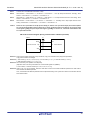
18. Cautions of flash memory programming by self-programming added (page 1142)
Refer to No.39 (page 50) in this document.
(c) 2013. Renesas Electronics Corporation. All rights reserved.
Page 29 of 50
RENESAS TECHNICAL UPDATE TN-RL*-A004C/E
Date: October , 2013
19. Items of flash memory programming characteristics added (page 1231)
Incorrect:
34.10 Flash memory programming characteristics
(TA = −40 to +85C, 1.8 V EVDD0 = EVDD1 VDD 5.5 V, VSS = EVSS0 = EVSS1 = 0 V)
Parameter
CPU/peripheral hardware clock
Symbol
Conditions
MIN.
fCLK
1.8 V VDD 5.5 V
Cerwr
1 erase + 1 write
Retained for 20 years
after the erase is
(Self/serial
regarded as 1
programming)
rewrite.
Retained for 1 years
TYP.
1
MAX.
Unit
32
MHz
frequency
Number of code flash rewrites
Number of data flash rewrites
The retaining years
are until next rewrite
after the rewrite.
1,000
Times
Note
1,000,000
(Self/serial
programming)
Note
Retained for 5 years
100,000
(Self/serial
programming)
Note
Note
When using flash memory programmer and Renesas Electronics self programming library.
Correct:
(TA = −40 to +85C, 1.8 V EVDD0 = EVDD1 VDD 5.5 V, VSS = EVSS0 = EVSS1 = 0 V)
Parameter
CPU/peripheral hardware
clock frequency
Symbol
fCLK
Number of code
flash rewrites
Notes 1,2,3
Cerwr
Conditions
MIN.
1.8 V VDD 5.5 V
TYP.
1
Retaining years: 20 years
Ta = 85C
Retaining year: 1 year
Ta = 25C
Retaining years: 5 years
Ta = 85C
100,000
Retaining years: 20 years
Ta = 85C
10,000
MAX.
Unit
32
MHz
1,000
1,000,000
Times
Number of data flash
rewrites
Notes 1
Notes 1,2,3
1 erase + 1 write after the erase is regarded as 1 rewrite.
The retaining years are until next rewrite after the rewrite.
2. When using flash memory programmer and Renesas Electronics self-programming library.
3. This characteristics is shown as the flash memory characteristics and based on Renesas Electronics reliability test.
(c) 2013. Renesas Electronics Corporation. All rights reserved.
Page 30 of 50
RENESAS TECHNICAL UPDATE TN-RL*-A004C/E
Date: October , 2013
20. 3.1.3 Internal Data Memory Space (page 105)
Incorrect:
Correct:
Cautions 2. The internal RAM in the following products cannot be used as stack area
when using the self-programming function and data flash function.
Cautions 2. While self-programming is being executed or rewriting the data flash, do not
allocate the RAM address which is used in stack, data buffer, the branch of
vectored interrupt servicing, or the transfer destination or source by DTC in the
address between FFE20H to FFEDFH.
R5F104xD (x = A to C, E to G, J, L) : FE900H to FED09H
R5F104xE (x = A to C, E to G, J, L) : FE900H to FED09H
R5F104xJ (x = F, G, J, L, M, P) : F9F00H to FA309H
3. The internal RAM area in the following products cannot be used as stack
memory when using the on-chip debugging trace function.
R5F104xJ (x = A to C, E to G, J, L): FA300H to FA6FFH
3. The RAM area in the products listed below cannot be used when using the
self-programming function or rewriting the data flash, because they are used by
libraries.
R5F104xD (x = A to C, E to G, J, L ) : FE900H to FED09H
R5F104xE (x = A to C, E to G, J, L ) : FE900H to FED09H
R5F104xJ (x = F, G, J, L, M, P) : F9F00H to FA309H
4. The internal RAM area in the following products cannot be used as stack memory
when using the on-chip debugging trace function.
R5F104xJ (x = A to C, E to G, J, L): FA300H to FA6FFH
(c) 2013. Renesas Electronics Corporation. All rights reserved.
Page 31 of 50
RENESAS TECHNICAL UPDATE TN-RL*-A004C/E
Date: October , 2013
21. 17.7.3 SNOOZE mode function (page 847)
Incorrect:
Correct:
When RxDq pin input is detected while in the STOP mode, the SNOOZE mode makes
data reception that does not require the CPU possible. Only following UARTs can be
specified for the reception baud rate adjustment function.
SNOOZE mode makes UART operate reception by RxDq pin input detection while the STOP
mode. Normally UART stops communication in the STOP mode. But, using the SNOOZE
mode makes reception UART operate unless the CPU operation by detecting RxDq pin input.
Only following channels can be set to the SNOOZE mode.
•
•
30 to 64-pin products: UART0 only
80 to 100-pin products: UART0 and UART2
•
•
When using the SNOOZE mode function, set the SWCm bit of serial standby control register m
(SSCm) to 1 just before switching to the STOP mode.
Cautions: 1. The SNOOZE mode can only be specified when the high-speed on-chip oscillator
clock is selected for fCLK.
2. The maximum transfer rate when using UARTq in the SNOOZE mode is
9600 bps (target).
30 to 64-pin products: UART0
80 to 100-pin products: UART0 and UART2
When using UARTq in SNOOZE mode, execute the following settings before entering STOP
mode (Refer to Flowcharts of SNOOZE mode operation in Figure 17-118 and Figure 17-120).
•
In SNOOZE mode, UART reception baud rate must be set differently from normal
operation. Refer to Table 17-3 to set registers SPSm and SDRmn [15:9].
•
Set bits EOCmn and SSECmn to enable or disable the error interrupt (INTSRE0) when a
communication error occurs.
•
Set the SWCm bit in the serial standby control register m (SSCm) to 1 just before entering
STOP mode. After initialization, set the SSm1 bit to 1 in the serial channel start register m
(SSm).
When the MCU detects the RxDq pin edge input (input the start bit) after entering STOP mode,
the UART reception is started.
Cautions 1. The SNOOZE mode can only be specified when the high-speed on-chip oscillator
clock (fIH) is selected for fCLK. Note that SNOOZE mode cannot be used when the
high-speed on-chip oscillator clock (fIH) is specified either as 64 or 48 MHz
2. The transfer rate in SNOOZE mode is 4800 bps only
3. When the SWCm bit is 1, UARTq can be used only when the reception is started
in STOP mode. If UARTq is used with other SNOOZE function or interrupts
concurrently and the reception is started in state other than STOP mode as
described below, the UARTq cannot receive data correctly and may cause a
framing error or parity error.
• When the UARTq reception is started from the moment the SWCm bit is set to 1
before the MCU enters STOP mode
• When the UARTq reception is started in SNOOZE mode
• When the UARTq reception is started from the moment the MCU exits STOP
mode and enters normal mode using interrupts before the SWCm bit is set to 0
(c) 2013. Renesas Electronics Corporation. All rights reserved.
Page 32 of 50
RENESAS TECHNICAL UPDATE TN-RL*-A004C/E
Date: October , 2013
4. When the SSECm bit is 1, if a parity error, framing error, or overrun error occurs,
flags PEFmn, FEFmn, or OVFmn is not set, nor an error interrupt (INTSREq) is
generated. To set the SSECm bit to 1, clear flags PEFmn, FEFmn, and OVFmn
before setting the SWC0 bit to 1, and read bits 7 to 0 (RxDq) in the SDRm1
register.
Table 17-3 UART Reception Baud Rate Setting in SNOOZE Mode
High-speed on-chip
UART reception baud rate in SNOOZE mode
oscillator
(fIH)
Baud rate: 4800 bps
Operating clock
SDRmn
Maximum
Minimum
(fMCK)
[15:9]
acceptable value
acceptable value
32 MHz ± 1.0%
(note)
fCLK /2
5
105
2.27%
−1.53%
24 MHz ± 1.0%
(note)
fCLK /2
5
79
1.60%
−2.18%
16 MHz ± 1.0%
(note)
fCLK /2
4
105
2.27%
−1.53%
12 MHz ± 1.0%
(note)
fCLK /2
4
79
1.60%
−2.19%
8 MHz ± 1.0%
(note)
fCLK /2
3
105
2.27%
−1.53%
6 MHz ± 1.0%
(note)
fCLK /2
3
79
1.60%
−2.19%
4 MHz ± 1.0%
(note)
fCLK /2
2
105
2.27%
−1.53%
3 MHz ± 1.0%
(note)
fCLK /2
2
79
1.60%
−2.19%
2 MHz ± 1.0%
(note)
fCLK /2
1
105
2.27%
−1.54%
1 MHz ± 1.0%
(note)
fCLK /2
0
105
2.27%
−1.57%
Note:
When the high-speed on-chip oscillator clock accuracy is at ± 1.5% or 2.0%, the
acceptable range is limited as follows:
• fIH ± 1.5%: Subtract 0.5% from the maximum acceptable value of fIH ± 1.0%, and
add 0.5% to the minimum acceptable value of fIH ± 1.0%.
• fIH ± 2.0%: Subtract 1.0% from the maximum acceptable value of fIH ± 1.0%, and
add 1.0% to the minimum acceptable value of fIH ± 1.0%.
Remarks: Maximum and minimum acceptable values in the above table are the baud rate
acceptable values in UART reception. Make sure to set the baud rate for
transmission within this range.
(c) 2013. Renesas Electronics Corporation. All rights reserved.
Page 33 of 50
RENESAS TECHNICAL UPDATE TN-RL*-A004C/E
Date: October , 2013
22. 23.2.2 STOP Mode (page 1050, 1052)
Refer to No.37 (pages 38 to 40) in this document.
23. 23.2.3 SNOOZE Mode (page 1055)
Refer to No.37 (page 42) in this document.
24. 27.3.6 Invalid memory access detection function (page 1105)
Refer to No.38 (page 48) in this document.
(c) 2013. Renesas Electronics Corporation. All rights reserved.
Page 34 of 50
RENESAS TECHNICAL UPDATE TN-RL*-A004C/E
Date: October , 2013
25. Figure 29-3 Format of Option Byte (000C2H/010C2H) (page 1121)
Old:
New:
Figure 29-3 Format of Option Byte (000C2H/010C2H)
Figure 29-3. Format of Option Byte (000C2H/010C2H)
Address: 000C2H/010C2H note
Address: 000C2H/010C2H
note
7
6
5
4
3
2
1
0
7
6
5
4
3
2
1
0
CMODE1
C5MODE0
1
0
FRQSEL3
FRQSEL2
FRQSEL1
FRQSEL0
CMODE1
C5MODE0
1
0
FRQSEL3
FRQSEL2
FRQSEL1
FRQSEL0
Setting of flash operation mode
CMODE1
CMODE0
0
0
LV (low voltage main) mode
1
0
LS (low speed main) mode
1
1
Other than above
FRQSEL4
FRQSEL3
HS (high speed main) mode
Setting of flash operation mode
Operating Frequency
Range
Operating Voltage
Range
CMODE1
CMODE0
1 to 4 MHz
1.6 to 5.5 V
0
0
LV (low voltage main) mode
1
0
LS (low speed main) mode
1 to 8 MHz
1.8 to 5.5 V
1 to 16 MHz
2.4 to 5.5 V
1 to 32 MHz
2.7 to 5.5 V
Setting prohibited
FRQSEL2
1
Other than above
FRQSEL1
FRQSEL0
Frequency of the high-speed
on-chip oscillator
fHOCO
1
0
0
0
64 MHz
32 MHz
1
0
0
0
0
48 MHz
24 MHz
0
1
0
0
0
32 MHz
32 MHz
0
0
0
0
0
24 MHz
24 MHz
0
1
0
0
1
16 MHz
16 MHz
0
0
0
0
1
12 MHz
12 MHz
0
1
0
1
0
8 MHz
8 MHz
0
1
0
1
1
4 MHz
4 MHz
0
1
1
0
1
1 MHz
1 MHz
Other than above
Operating Voltage
Range
1 to 4 MHz
1.6 to 5.5 V
1 to 8 MHz
1.8 to 5.5 V
HS (high speed main) mode
Setting prohibited
Set the same value as 000C2H to 010C2H when the boot swap operation is used
because 000C2H is replaced by 010C2H.
1 to 16 MHz
2.4 to 5.5 V
1 to 32 MHz
2.7 to 5.5 V
Setting prohibited
Frequency of the high-speed
on-chip oscillator
FRQSEL4
FRQSEL3
FRQSEL2
FRQSEL1
FRQSEL0
1
1
0
0
0
64 MHz
32 MHz
1
0
0
0
0
48 MHz
24 MHz
32 MHz
fIH
1
Note:
1
Operating Frequency
Range
fHOCO
fIH
0
1
0
0
0
32 MHz
0
0
0
0
0
24 MHz
24 MHz
0
1
0
0
1
16 MHz
16 MHz
0
0
0
0
1
12 MHz
12 MHz
0
1
0
1
0
8 MHz
8 MHz
0
0
0
1
0
6 MHz
6 MHz
0
1
0
1
1
4 MHz
4 MHz
0
0
0
1
1
3 MHz
3 MHz
0
1
1
0
0
2 MHz
2 MHz
0
1
1
0
1
1 MHz
1 MHz
Other than above
Note:
Setting prohibited
Set the same value as 000C2H to 010C2H when the boot swap operation is used
because 000C2H is replaced by 010C2H.
Caution:
Be sure to set bit 5 to 1 and bit 4 to 0.
(c) 2013. Renesas Electronics Corporation. All rights reserved.
Page 35 of 50
RENESAS TECHNICAL UPDATE TN-RL*-A004C/E
Date: October , 2013
26. 34.4.1 Pin characteristics (pages 1181, 1182)
Correct:
Refer to pages 5 and 6 in Technical Update Exhibit “Chapter 34 ELECTRICAL
SPECIFICATIONS (A, D: TA = −40 to + 85°C)”.
Incorrect:
Fixed typo in Note 3 in pages 1181 and 1182
27. 34.4.2 Supply current characteristics (pages 1186 to 1195)
Incorrect:
Fixed typo in Notes and typical values of IDD2 and IDD3 in pages 1186 to 1195
28. 34.5 AC Characteristics (pages 1196, 1197)
Old:
Specifications of the external system clock frequency and external system clock input
high-level width, low-level width in page 1196 to 1197 extended
29. 34.6.1 Serial array unit (pages 1198 to 1221)
Correct:
Refer to pages 10 to 16 in Technical Update Exhibit “Chapter 34 ELECTRICAL
SPECIFICATIONS (A, D: TA = −40 to + 85°C)”.
New:
Refer to page 20 in Technical Update Exhibit “Chapter 34 ELECTRICAL SPECIFICATIONS (A,
D: TA = −40 to + 85°C)”.
Correct:
Refer to pages 27 to 54 in Technical Update Exhibit “Chapter 34 ELECTRICAL
SPECIFICATIONS (A, D: TA = −40 to + 85°C)”.
Incorrect:
Fixed typo in 34.6.1 Serial array unit in pages 1198 to 1221
30. 34.6.2 Serial Interface IICA (page 1222)
Incorrect:
Fixed typo in 34.6.2 Serial interface IICA in page 1222
Correct:
Refer to pages 55 to 58 in Technical Update Exhibit “Chapter 34 ELECTRICAL
SPECIFICATIONS (A, D: TA = −40 to + 85°C)”.
31. 34.7.1 A/D converter characteristics (pages 1223 to 1226)
Old:
Specifications of “34.7.1 A/D converter characteristics” in pages 1223 to 1226 extended
New:
Refer to pages 59 to 62 in Technical Update Exhibit “Chapter 34 ELECTRICAL
SPECIFICATIONS (A, D: TA = −40 to + 85°C)”.
32. 34.7.2 Temperature Sensor/Internal Reference Voltage
Characteristics (page 1227)
Incorrect:
Fixed typo in 34.7.2 Temperature Sensor/Internal Reference Voltage Characteristics in page
1227
33. 34.7.5 POR circuit characteristics (page 1228)
Correct:
Refer to page 64 in Technical Update Exhibit “Chapter 34 ELECTRICAL SPECIFICATIONS
(A, D: TA = −40 to + 85°C)”.
Incorrect:
Fixed typo in 34.7.5 POR circuit characteristics in page 1228
(c) 2013. Renesas Electronics Corporation. All rights reserved.
Correct:
Refer to page 63 in Technical Update Exhibit “Chapter 34 ELECTRICAL SPECIFICATIONS
(A, D: TA = −40 to + 85°C)”.
Page 36 of 50
RENESAS TECHNICAL UPDATE TN-RL*-A004C/E
Date: October , 2013
34. Supply Voltage Rise Time
New:
Refer to page 66 in Technical Update Exhibit “Chapter 34 ELECTRICAL SPECIFICATIONS
(A, D: TA = −40 to + 85°C)”.
Old:
Specifications in Supply Voltage Rise Time in page 1231 added
35. 34.9 Data Memory STOP Mode Low Supply Voltage Data Retention
Characteristics (page 1231)
Old:
Specifications in Data Memory STOP Mode Low Supply Voltage Data Retention
Characteristics in page 1231 extended
New:
Refer to page 67 in Technical Update Exhibit “Chapter 34 ELECTRICAL SPECIFICATIONS
(A, D: TA = −40 to + 85°C)”.
36. Chapter 35 ELECTRICAL SPECIFICATIONS (G: TA = −40 to +105°C)
Old:
Specifications in Chapter 35 ELECTRICAL SPECIFICATIONS (G: TA = −40 to +105°C) fixed
(c) 2013. Renesas Electronics Corporation. All rights reserved.
Page 37 of 50
New:
Refer to pages 1 to 58 in Technical Update Exhibit “Chapter 35 ELECTRICAL
SPECIFICATIONS (G: TA = −40 to +105°C)”.
RENESAS TECHNICAL UPDATE TN-RL*-A004C/E
Date: October , 2013
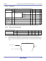
37. Incorrect descriptions of reset processing time/standby mode
release time revised
Incorrect descriptions of reset processing time revised (page 1049)
Incorrect:
Correct:
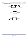
Figure 23-4 HALT Mode Release by Reset (1/2)
Figure 23-4 HALT Mode Release by Reset (1/2)
(Omitted)
(Omitted)
(2) When high-speed on-chip oscillator clock is used as CPU clock
(2) When high-speed on-chip oscillator clock is used as CPU clock
(Omitted)
(Omitted)
Reset processing time when HALT mode or STOP mode is released
Reset processing time: 387 to 720 s (When LVD is used)
155 to 407 s (When LVD off)
Note:
Refer to Chapter 24 RESET FUNCTION for the reset processing time. For details
about the reset processing time for power-on-reset (POR) circuit and voltage detector
(LVD), refer to Chapter 25 POWER-ON-RESET CIRCUIT.
Figure 23-4 HALT Mode Release by Reset (2/2)
Figure 23-4 HALT Mode Release by Reset (2/2)
(3) When subsystem clock is used as CPU clock
(Omitted)
(3) When subsystem clock is used as CPU clock
(Omitted)
Note:
Reset processing time when HALT mode or STOP mode is released
Reset processing time: 387 to 720 s (When LVD is used)
155 to 407 s (When LVD off)
(c) 2013. Renesas Electronics Corporation. All rights reserved.
Page 38 of 50
Refer to Chapter 24 RESET FUNCTION for the reset processing time. For details
about the reset processing time for power-on-reset (POR) circuit and voltage detector
(LVD), refer to Chapter 25 POWER-ON-RESET CIRCUIT.
RENESAS TECHNICAL UPDATE TN-RL*-A004C/E
Date: October , 2013
Incorrect descriptions of reset processing time revised (pages 1052 to 1054)
Incorrect:
Correct:
(2) STOP mode release
(2) STOP mode release
The STOP mode can be released by the following two sources.
The STOP mode can be released by the following two sources.
(a) Release by unmasked interrupt request
(a) Release by unmasked interrupt request
When an unmasked interrupt request is generated, the STOP mode is released. After the
oscillation stabilization time has elapsed, if interrupt acknowledgement is enabled, vectored
interrupt servicing is carried out. If interrupt acknowledgement is disabled, the next address
instruction is executed.
When an unmasked interrupt request is generated, the STOP mode is released. After the
oscillation stabilization time has elapsed, if interrupt acknowledgement is enabled, vectored
interrupt servicing is carried out. If interrupt acknowledgement is disabled, the next address
instruction is executed.
Figure 23-5 STOP Mode Release by Interrupt Request Generation (1/2)
Figure 23-5 STOP Mode Release by Interrupt Request Generation (1/2)
(1) When high-speed system clock (X1 oscillation) is used as CPU clock
(1) When high-speed system clock (X1 oscillation) is used as CPU clock
(Omitted)
(Omitted)
Note 1. For details of the standby release signal, see Figure 21-1 Basic Configuration of
Interrupt Function.
Note Wait time for STOP mode release
High-speed system clock (X1 oscillation): 3-clock
Note 2. STOP mode release time
Supply of the clock is stopped:
• When FRQSEL4 = 0: 18 µs to “whichever is longer 65 µs or the oscillation
stabilization time (set by OSTS)”
• When FRQSEL4 = 1: 18 µs to “whichever is longer 135 µs or the oscillation
stabilization time (set by OSTS)”
Wait:
• When vectored interrupt servicing is carried out: 10 to 11 clocks
• When vectored interrupt servicing is not carried out: 4 to 5 clocks
Caution:
Remark 1.
To reduce the oscillation stabilization time after release from the STOP mode
while CPU operates based on the high-speed system clock (X1 oscillation), switch
the clock to the high-speed on-chip oscillator clock temporarily before executing the
STOP instruction.
The clock supply stop time varies depending on the temperature conditions and
STOP mode period.
Remark 2. The broken lines indicate the case when the interrupt request that has released
the standby mode is acknowledged.
(c) 2013. Renesas Electronics Corporation. All rights reserved.
Page 39 of 50
RENESAS TECHNICAL UPDATE TN-RL*-A004C/E
Date: October , 2013
Figure 23-5 STOP Mode Release by Interrupt Request Generation (2/2)
Figure 23-5 STOP Mode Release by Interrupt Request Generation (2/2)
(2) When high-speed system clock (external clock input) is used as CPU clock
(2) When high-speed system clock (external clock input) is used as CPU clock
(Omitted)
(Omitted)
Note 1. For details of the standby release signal, see Figure 21-1 Basic Configuration of
Interrupt Function.
Note 2. STOP mode release time
Supply of the clock is stopped:
• When FRQSEL4 = 0: 18 µs to 65 µs
• When FRQSEL4 = 1: 18 µs to 135 µs
Wait:
• When vectored interrupt servicing is carried out: 7 clocks
• When vectored interrupt servicing is not carried out: 1 clock
(3) When high-speed on-chip oscillator clock is used as CPU clock
(3) When high-speed on-chip oscillator clock is used as CPU clock
(Omitted)
(Omitted)
Note STOP mode release time:
High-speed system clock (external clock input): 19.1 to 31.98 s
High-speed on-chip oscillator clock: 19.1 to 31.98 s
Note 1. For details of the standby release signal, see Figure 21-1 Basic Configuration of
Interrupt Function.
Note 2. STOP mode release time
Supply of the clock is stopped:
• When FRQSEL4 = 0: 18 µs to 65 µs
• When FRQSEL4 = 1: 18 µs to 135 µs
Wait:
• When vectored interrupt servicing is carried out: 7 clocks
• When vectored interrupt servicing is not carried out: 1 clock
Remark 1.
Remark 2.
(c) 2013. Renesas Electronics Corporation. All rights reserved.
Page 40 of 50
The clock supply stop time varies depending on the temperature conditions and
STOP mode period.
The broken lines indicate the case when the interrupt request that has released
the standby mode is acknowledged.
RENESAS TECHNICAL UPDATE TN-RL*-A004C/E
Date: October
(b) Release by reset signal generation
(b) Release by reset signal generation
When the reset signal is generated, STOP mode is released, and then, as in the case with a
normal reset operation, the program is executed after branching to the reset vector address.
When the reset signal is generated, STOP mode is released, and then, as in the case with a
normal reset operation, the program is executed after branching to the reset vector address.
Figure 23-6 STOP Mode Release by Reset
Figure 23-6 STOP Mode Release by Reset
(1) When high-speed system clock is used as CPU clock
(1) When high-speed system clock is used as CPU clock
(Omitted)
(Omitted)
(2) When high-speed on-chip oscillator clock is used as CPU clock
(2) When high-speed on-chip oscillator clock is used as CPU clock
(Omitted)
(Omitted)
Note:
Reset processing time when HALT mode or STOP mode is released
Reset processing time: 387 to 720 s (When LVD is used)
155 to 407 s (When LVD off)
(c) 2013. Renesas Electronics Corporation. All rights reserved.
Page 41 of 50
Refer to Chapter 24 RESET FUNCTION for the reset processing time. For details
about the reset processing time for power-on-reset (POR) circuit and voltage detector
(LVD), refer to Chapter 25 POWER-ON-RESET CIRCUIT.
RENESAS TECHNICAL UPDATE TN-RL*-A004C/E
Date: October , 2013
Explanations of SNOOZE mode shift time added (page 1055)
Incorrect:
Correct:
23.2.3 SNOOZE mode
23.2.3 SNOOZE mode
(1) SNOOZE mode setting and operating statuses
(1) SNOOZE mode setting and operating statuses
(Omitted)
(Omitted)
The operating statuses in the SNOOZE mode are shown below.
In SNOOZE mode transition, wait status to be only following time.
When FRQSEL4 = 0: 18 µs to 65 µs
When FRQSEL4 = 1: 18 µs to 135 µs
Remark: Transition time from STOP mode to SNOOZE mode varies depending on the
temperature conditions and the STOP mode period.
Transition time from SNOOZE mode to normal operation:
• When vectored interrupt servicing is carried out:
HS (High-speed main) mode: “4.99 µs to 9.44 µs” + 7 clocks
LS (Low-speed main) mode: “1.10 µs to 5.08 µs” + 7 clocks
LV (Low-voltage main) mode: “16.58 µs to 25.40 µs” + 7 clocks
• When vectored interrupt servicing is not carried out:
HS (High-speed main) mode: “4.99 µs to 9.44 µs” + 1 clock
LS (Low-speed main) mode: “1.10 µs to 5.08 µs” + 1 clock
LV (Low-voltage main) mode: “16.58 µs to 25.40 µs” + 1 clock
The operating statuses in the SNOOZE mode are shown next
(c) 2013. Renesas Electronics Corporation. All rights reserved.
Page 42 of 50
RENESAS TECHNICAL UPDATE TN-RL*-A004C/E
Date: October , 2013
Incorrect descriptions of reset processing time revised (pages 1060, 1061)
Correct:
______________
Figure 24-2 Timing of Reset by R E S E T Input
Incorrect:
______________
Figure 24-2 Timing of Reset by R E S E T Input
Release from the reset state is automatic in case of a reset due to a watchdog time overflow,
execution of an illegal instruction, detection of a RAM parity error, or detection of illegal
memory access. After reset processing, program execution starts with the high-speed on-chip
oscillator clock as the operating clock.
Figure 24-3 Timing of Reset Due to Execution of Illegal Instruction or Watchdog Timer Overflow
Figure 24-3 Timing of Reset Due to Watchdog Timer Overflow, Execution of Illegal Instruction,
Detection of RAM Parity Error, or Detection of Illegal Memory Access
(c) 2013. Renesas Electronics Corporation. All rights reserved.
Page 43 of 50
RENESAS TECHNICAL UPDATE TN-RL*-A004C/E
Date: October , 2013
______________
______________
Figure 24-4 Timing of Reset in STOP mode by R E S E T Input
Note When P130 is set to high-level output before reset is effected, the output signal of P130
can be dummy-output as a reset signal to an external device, because P130 outputs a
low level when reset is effected. To release a reset signal to an external device, set
P130 to high-level output by software.
Remark For the reset timing of the power-on-reset circuit and voltage detector, see Chapter
25 POWER-ON-RESET CIRCUIT and Chapter 26 VOLTAGE DETECTOR.
Figure 24-4 Timing of Reset in STOP mode by R E S E T Input
Notes:
1: When P130 is set to high-level output before reset is effected, the output signal of P130
can be dummy-output as a reset signal to an external device, because P130 outputs a low
level when reset is effected. To release a reset signal to an external device, set P130 to
high-level output by software.
2. Reset processing time when an external reset is released:
The first reset processing time after POR is released:
0.672 ms (TYP.), 0.832 ms (max.) (When LVD is used)
0.399 ms (TYP.), 0.519 ms (max.) (When LVD is off)
The second and subsequent reset processing time after POR is released:
0.531 ms (TYP.), 0.675 ms (max.) (When LVD is used)
0.259 ms (TYP.), 0.362 ms (max.) (When LVD is off)
After power is supplied, a voltage stabilization wait time of about 0.99 ms (TYP.) and up to
2.30 ms (MAX.) is required before reset processing starts after the external reset is
released.
3. The state of P40 is as follows:
• High-impedance during the external reset period or reset period by the POR.
• High level during other types of reset or after receiving a reset signal (connected to the
on-chip pull-up resistor).
Reset by POR and LVD circuit supply voltage detection is automatically released when
VDD ≥ VPOR or VDD ≥ VLVD after the reset. After reset processing, execution of the program
with the high-speed on-chip oscillator clock as the operating clock starts. For details, see
Chapter 25 POWER-ON-RESET CIRCUIT or Chapter 26 VOLTALGE DETECTOR.
(c) 2013. Renesas Electronics Corporation. All rights reserved.
Page 44 of 50
RENESAS TECHNICAL UPDATE TN-RL*-A004C/E
Date: October , 2013
Incorrect descriptions of reset processing time revised (pages 1072, 1073)
Correct:
Figure 25-2. Timing of Generation of Internal Reset Signal by
Power-on-reset Circuit and Voltage Detector (1/2)
Incorrect:
______________
(1) When using an external reset by the R E S E T pin
Figure 25-2. Timing of Generation of Internal Reset Signal by
Power-on-reset Circuit and Voltage Detector (1/2)
(1) When LVD is OFF (option byte 000C1H/010C1H: VPOC2 = 1B)
Supply voltage
(VDD)
Operating voltage
range lower limit Note 1
VPOR = 1.51 V (TYP.)
VPDR = 1.50 V (TYP.)
Supply voltage
(VDD)
Operating voltage
range lower limit Note 1
VPOR = 1.51 V (TYP.)
VPDR = 1.50 V (TYP.)
10 µs or more
10 µs or more
0V
10 µs or more
RESET pin
Wait for oscillation
accuracy stabilization Note 2
Wait for oscillation
accuracy stabilizationNote 2
RESET pin
Wait for oscillation
accuracy stabilization Note 2
Wait for oscillation
accuracy stabilization Note 2
High-speed on-chip
oscillator clock (f IH)
High-speed on-chip
oscillator clock (fIH)
Starting oscillation is
specified by software
High-speed
system clock (fMX)
(when X1 oscillation
is selected)
Internal reset signal
Operation
stops
CPU
Reset processing Note 4
High-speed system
clock (fMX)
(when X1 oscillation
is selected)
Starting oscillation is
specified by software
Normal operation
(high-speed on-chip
oscillator clock) Note 3
Reset
period
(oscillation
stop)
CPU Operation stops
Reset processing
Normal operation
(high-speed on-chip
oscillator clock) Note 3
Starting oscillation is
specified by software
Starting oscillation is
specified by software
Normal operation
(high-speed on-chip
oscillator clock) Note 3
Reset
period
(oscillation stops)
Normal operation
(high-speed on-chip
oscillator clock) Note 3
Operation stops
Note 4
Note 4
Reset processing time when an external reset is released
Voltage stabilization wait time: 0.99 ms (TYP.), 2.30 ms (max.)
Operation stops
Reset processing time when an external reset is released
Voltage stabilization wait time: 0.99 ms (TYP.), 2.30 ms (max.)
Internal reset signal
Internal reset signal
Notes 4. Reset processing time: 155 to 407 µs
Note 4. Before the MCU starts normal operation, it waits until the voltage becomes stable
(voltage stabilization wait time after the voltage reaches VPOR (1.51 V, TYP.), and
also requires the following “reset processing time when an external reset is released”
after the RESET signal is set to 1 (high level).
Reset processing time when an external reset is released:
0.672 ms (TYP.), 0.832 ms (max.) (When LVD is used)
0.399 ms (TYP.), 0.519 ms (max.) (When LVD is off)
Note 5. The second and subsequent reset processing time after POR is released:
0.531 ms (TYP.), 0.675 ms (max.) (When LVD is used)
0.259 ms (TYP.), 0.362 ms (max.) (When LVD is off)
(Go on to the next page)
(c) 2013. Renesas Electronics Corporation. All rights reserved.
Page 45 of 50
RENESAS TECHNICAL UPDATE TN-RL*-A004C/E
Date: October , 2013
Figure 25-2. Timing of Generation of Internal Reset Signal by
Power-on-reset Circuit and Voltage Detector (2/2)
(2) LVD is interrupt & reset mode (option byte 000C1H/010C1H: LVIMDS1, LVIMDS0 = 1, 0)
(2) When LVD is in interrupt& reset mode
Supply voltage
(VDD)
VLVDH
VLVDL
(option byte 000C1H/010C1H: LVIMDS1, LVIMDS0 = 1, 0)
Supply voltage
(VDD)
VLVIH
VLVIL
Operating voltage
range lower limit Note 1
VPOR = 1.51 V (TYP.)
VPDR = 1.50 V (TYP.)
Note 4
Note 1
Operating voltage range lower limit
VPOR = 1.51 V (TYP.)
VPDR = 1.50 V (TYP.)
Note 4
0V
Wait for oscillation Note 3
accuracy stabilization
Wait for oscillation Note 3
accuracy stabilization
0V
Wait for oscillation
accuracy stabilization Note 3
Wait for oscillation
accuracy stabilization Note 3
High-speed on-chip
oscillator clock (fIH)
High-speed
system clock (fMX)
(when X1 oscillation
is selected)
Operation
stops
CPU
Starting oscillation is
specified by software
High-speed on-chip
oscillator clock (fIH)
High-speed system
clock (fMX)
(when X1 oscillation
Starting oscillation is
specified by software
Normal operation
(high-speed on-chip
oscillator clock) Note 2
Reset processing time
Note 5
POR processing time
Reset
period
(oscillation
stop)
Normal operation
(high-speed on-chip
oscillator clock)Note 2
Normal operation
(high-speed on-chip
oscillator clock) Note 2
is selected)
CPU Operation stops
Reset period
(oscillation stops)
LVD reset processing time Note 5
Voltage stabilization wait time + POR processing time:
1.64 ms (TYP.), 3.10 ms (max.)
Normal operation
(high-speed on-chip
oscillator clock) Note 2
Operation stops
LVD reset processing time Note 5
Voltage stabilization wait time + POR processing time:
1.64 ms (TYP.), 3.10 ms (max.)
Operation stops
Reset processing time
POR processing time
Internal reset signal
Internal reset signal
INTLVI
INTLVI
Notes
Starting oscillation is
specified by software
Starting oscillation is
specified by software
(Omitted)
Note 5. Before the MCU starts normal operation, it requires the voltage stabilization wait time
5. Reset processing time: 387 to 720 µs
+ POR processing time after the voltage reaches VPOR (1.51 V, TYP.), and also
requires the following “LVD reset processing time” after the voltage reaches the LVD
detection level (VLVDH).
LVD reset processing time: 0 ms (TYP.) to 0.0701 ms (max.)
(Go on to the next page)
(c) 2013. Renesas Electronics Corporation. All rights reserved.
Page 46 of 50
RENESAS TECHNICAL UPDATE TN-RL*-A004C/E
Date: October , 2013
(3) When LVD is in reset mode (option byte 000C1H LVIMDS1, LVIMDS0 = 1, 1)
Supply voltage
(VDD)
VLVDH
VLVDL
Operating voltage range lower limit
Note 1
VPOR = 1.51 V (TYP.)
VPDR = 1.50 V (TYP.)
0V
Wait for oscillation Note 3
accuracy stabilization
Wait for oscillation Note 3
accuracy stabilization
High-speed on-chip
oscillator clock (fIH)
High-speed system
clock (fMX)
(when X1 oscillation
is selected)
CPU Operation stops
Starting oscillation is
specified by software
Reset period
Normal operation
(oscillation
(high-speed on-chip stops)
oscillator clock)Note 2
Wait for oscillation Note 3
accuracy stabilization
Starting oscillation is
specified by software
Starting oscillation is
specified by software
Normal operation
(high-speed on-chip
oscillator clock) Note 2
Reset period
(oscillation stops)
Normal operation
(high-speed on-chip
oscillator clock) Note 2
Note 4
Note 4
Voltage stabilization wait time + POR processing time:
1.64 ms (TYP.), 3.10 ms (max.)
Operation stops
LVD reset processing time
LVD reset processing time
LVD reset processing time
Note 5
Voltage stabilization wait time + POR processing time:
1.64 ms (TYP.), 3.10 ms (max.)
Internal reset signal
Note 4. Before the MCU starts normal operation, it requires the voltage stabilization wait time
+ POR processing time after the voltage reaches VPOR (1.51 V, TYP.), and also
requires the following “LVD reset processing time” after the voltage reaches the LVD
detection level (VLVDH).
LVD reset processing time: 0 ms (TYP.) to 0.0701 ms (max.)
Note 5. When supply voltage falls and returns after only an internal reset occurs by the
voltage detector (LVD), it requires the following processing time after the voltage
reaches the LVD detection level (VLVDH).
LVD reset processing time: 0.0511 ms (TYP.) to 0.0701 ms (max.)
(c) 2013. Renesas Electronics Corporation. All rights reserved.
Page 47 of 50
RENESAS TECHNICAL UPDATE TN-RL*-A004C/E
Date: October 23, 2013
38. 27.3.6 Invalid memory access detection function (page 1105)
Incorrect:
Correct:
Figure 27-10 Invalid memory access detection function
Possibility access
Read
Write
Figure 27-10 Invalid memory access detection function
Fetching
instructions
(execute)
Accessibility
FFFFFH
Read
Special function register (SFR)
256 byte
FFF00H
FFEFFH
FFEE0H
FFEDFH
Write
Instruction fetch
(execution)
FFFFFH
Special function register (SFR)
256 bytes
NG
General-purpose register
32 byte
FFF00H
FFEFFH
OK
FFEE0H
FFEDFH
RAMNote
OK
NG
General-purpose register
32 bytes
OK
RAMNote
OK
yyyyyH
Mirror
zzzzzH
OK
Mirror
NG
NG
Data flash memory
F1000H
F0FFFH
OK
NG
NG
Data flash memory
Reserved
F1000H
F0FFFH
OK
F0800H
F07FFH
Reserved
Special function register (2nd SFR)
2 Kbyte
OK
F0800H
F07FFH
OK
OK
Special function register (2nd SFR)
2 Kbytes
NG
F0000H
EFFFFH
NG
F0000H
EFFFFH
OK
EF000H
EEFFFH
Reserved
NG
NG
OK
EF000H
EEFFFH
Reserved
NG
NG
NG
NG
yyyyyH
xxxxxH
xxxxxH
Code flash memory Note
Code flash memory Note
OK
OK
00000H
00000H
(c) 2013. Renesas Electronics Corporation. All rights reserved.
Page 48 of 50
OK
OK
RENESAS TECHNICAL UPDATE TN-RL*-A004C/E
Date: October 23, 2013
Note: Code flash memory and RAM address of each product are as follows.
Products
R5F104xA
(x = A to C, E to G)
R5F104xC
(x = A to C, E to G, J, L)
R5F104xD
(x = A to C, E to G, J, L)
R5F104xE
(x = A to C, E to G, J, L)
R5F104xF
(x = A to C, E to G, J, L, M, P)
R5F104xG
(x = A to C, E to G, J, L, M, P)
R5F104xH
(x = E to G, J, L, M, P)
R5F104xJ
(x = F, G, J, L, M, P)
Code flash memory
(00000H to xxxxxH)
16384 × 8 bit
(00000H to 03FFFH)
32768 × 8 bit
(00000H to 07FFFH)
49152 × 8 bit
(00000H to 0BFFFH)
65536 × 8 bit
(00000H to 0FFFFH)
98304 × 8 bit
(00000H to 17FFFH)
131072 × 8 bit
(00000H to 1FFFFH)
196608 × 8 bit
(00000H to 2FFFFH)
262144 × 8 bit
(00000H to 3FFFFH)
(c) 2013. Renesas Electronics Corporation. All rights reserved.
RAM
(yyyyyH to FFEFFH)
2560 × 8 bit
(FF500H to FFEFFH)
4096 × 8 bit
(FEF00H to FFEFFH)
5632 × 8 bit
(FE900H to FFEFFH)
5632 × 8 bit
(FE900H to FFEFFH)
12288 × 8 bit
(FCF00H to FFEFFH)
16384 × 8 bit
(FBF00H to FFEFFH)
20480 × 8 bit
(FAF00H to FFEFFH)
24576 × 8 bit
(F9F00H to FFEFFH)
Page 49 of 50
Note: Code flash memory area, RAM area, and the detected lowest address of each product
are as follows.
Products
Code flash memory
(00000H to xxxxxH)
RAM
(zzzzzH to FFEFFH)
R5F104xA
(x = A to C, E to G)
R5F104xC
(x = A to C, E to G, J, L)
R5F104xD
(x = A to C, E to G, J, L)
R5F104xE
(x = A to C, E to G, J, L)
R5F104xF
(x = A to C, E to G, J, L, M, P)
R5F104xG
(x = A to C, E to G, J, L, M, P)
R5F104xH
(x = E to G, J, L, M, P)
R5F104xJ
(x = F, G, J, L, M, P)
16384 × 8 bit
(00000H to 03FFFH)
32768 × 8 bit
(00000H to 07FFFH)
49152 × 8 bit
(00000H to 0BFFFH)
65536 × 8 bit
(00000H to 0FFFFH)
98304 × 8 bit
(00000H to 17FFFH)
131072 × 8 bit
(00000H to 1FFFFH)
196608 × 8 bit
(00000H to 2FFFFH)
262144 × 8 bit
(00000H to 3FFFFH)
2560 × 8 bit
(FF500H to FFEFFH)
4096 × 8 bit
(FEF00H to FFEFFH)
5632 × 8 bit
(FE900H to FFEFFH)
5632 × 8 bit
(FE900H to FFEFFH)
12288 × 8 bit
(FCF00H to FFEFFH)
16384 × 8 bit
(FBF00H to FFEFFH)
20480 × 8 bit
(FAF00H to FFEFFH)
24576 × 8 bit
(F9F00H to FFEFFH)
Detected lowest
address for
read/instruction
fetch (execution)
(yyyyyH)
10000H
10000H
10000H
10000H
20000H
20000H
30000H
40000H
RENESAS TECHNICAL UPDATE TN-RL*-A004C/E
Date: October 23, 2013
39. Cautions of flash memory programming by self-programming
added (page 1142)
Correct:
Incorrect:
30.7 Flash Memory Programming by Self-Programming
30.7 Flash Memory Programming by Self-Programming
(Omitted)
(Omitted)
Caution 1. The self-programming function cannot be used when the CPU operates with the
Caution 1. The self-programming function cannot be used when the CPU operates with the
subsystem clock.
Caution 2. To prohibit an interrupt during self-programming, in the same way as in the normal
operation mode, execute the self-programming library in the state where the IE flag
is cleared (0) by the DI instruction.
To enable an interrupt, clear (0) the interrupt
mask flag to accept in the state where the IE flag is set (1) by the EI instruction, and
subsystem clock.
Caution 2. To prohibit an interrupt during self-programming, in the same way as in normal
operation mode, execute the self-programming library in the state where the IE flag
is cleared (0) by the DI instruction. To enable an interrupt, clear (0) the interrupt
mask flag to accept in the state where the IE flag is set (1) by the EI instruction,
and then execute the self-programming library.
then execute the self-programming library.
Caution 3. When enabling RAM parity error resets (RPERDIS = 0), be sure to initialize the
Caution 3. When enabling RAM parity error resets (RPERDIS = 0), make sure to initialize the
RAM area to use + 10 bytes before overwriting.
RAM area to use + 10 bytes before overwriting.
Caution 4. The high-speed on-chip oscillator needs to keep oscillating during
self-programming. When the high-speed on-chip oscillator is stopped, oscillate
the high-speed on-chip oscillator clock (HIOSTOP = 0) and execute the flash
self-programming library after 30 µs elapsed when the FRQSEL4 in the user
option byte (000C2H) is 0; otherwise execute the flash self-programming library
after 80 µs elapsed.
(c) 2013. Renesas Electronics Corporation. All rights reserved.
Page 50 of 50
CHAPTER 34 ELECTRICAL SPECIFICATIONS (A, D: TA = -40 to +85 C)
RL78/G14
CHAPTER 34 ELECTRICAL SPECIFICATIONS (A, D: TA = -40 to +85 C)
This chapter describes the electrical specifications for the products “A: Consumer applications (TA = -40 to +85 C)” and
“D: Industrial applications (TA = -40 to +85 C)”.
Caution 1. The RL78 microcontrollers have an on-chip debug function, which is provided for development and
evaluation. Do not use the on-chip debug function in products designated for mass production,
because the guaranteed number of rewritable times of the flash memory may be exceeded when this
function is used, and product reliability therefore cannot be guaranteed. Renesas Electronics is not
liable for problems occurring when the on-chip debug function is used.
Caution 2. With products not provided with an EVDD0, EVDD1, EVSS0, or EVSS1 pin, replace EVDD0 and EVDD1 with
VDD, or replace EVSS0 and EVSS1 with VSS.
Caution 3. The pins mounted depend on the product. Refer to 2.1 Port Functions to 2.2.1 With functions for
each product.
1
CHAPTER 34 ELECTRICAL SPECIFICATIONS (A, D: TA = -40 to +85 C)
RL78/G14
34.1
Absolute Maximum Ratings
Absolute Maximum Ratings
Parameter
Supply voltage
REGC pin input voltage
(1/2)
Symbols
Conditions
Ratings
Unit
-0.5 to +6.5
V
EVDD0, EVDD1 EVDD0 = EVDD1
-0.5 to +6.5
V
EVSS0, EVSS1
EVSS0 = EVSS1
-0.5 to +0.3
V
VIREGC
REGC
-0.3 to +2.8
V
VDD
and -0.3 to VDD +0.3 Note 1
Input voltage
VI1
P00 to P06, P10 to P17, P30, P31,
P40 to P47, P50 to P57, P64 to P67,
-0.3 to EVDD0 +0.3
V
and -0.3 to VDD +0.3 Note 2
P70 to P77, P80 to P87, P100 to P102,
P110, P111, P120, P140 to P147
VI2
P60 to P63 (N-ch open-drain)
VI3
P20 to P27, P121 to P124, P137,
-0.3 to +6.5
-0.3 to VDD +0.3
V
Note 2
V
P150 to P156, EXCLK, EXCLKS, RESET
Output voltage
VO1
P00 to P06, P10 to P17, P30, P31,
P40 to P47, P50 to P57, P60 to P67,
-0.3 to EVDD0 +0.3
and -0.3 to VDD +0.3
V
Note 2
P70 to P77, P80 to P87, P100 to P102,
P110, P111, P120, P130, P140 to P147
Analog input voltage
VO2
P20 to P27, P150 to P156
VAI1
ANI16 to ANI20
-0.3 to VDD +0.3 Note 2
-0.3 to EVDD0 +0.3
and -0.3 to AVREF(+) +0.3 Notes 2, 3
VAI2
ANI0 to ANI14
-0.3 to VDD +0.3
and -0.3 to AVREF(+) +0.3 Notes 2, 3
Note 1.
V
V
V
Connect the REGC pin to VSS via a capacitor (0.47 to 1 F). This value regulates the absolute maximum rating of the
REGC pin. Do not use this pin with voltage applied to it.
Note 2.
Must be 6.5 V or lower.
Note 3.
Do not exceed AVREF (+) + 0.3 V in case of A/D conversion target pin.
Caution
Product quality may suffer if the absolute maximum rating is exceeded even momentarily for any parameter.
That is, the absolute maximum ratings are rated values at which the product is on the verge of suffering physical
damage, and therefore the product must be used under conditions that ensure that the absolute maximum
ratings are not exceeded.
Remark 1. Unless specified otherwise, the characteristics of alternate-function pins are the same as those of the port pins.
Remark 2. AVREF (+): + side reference voltage of the A/D converter.
Remark 3. VSS: Reference voltage
2
CHAPTER 34 ELECTRICAL SPECIFICATIONS (A, D: TA = -40 to +85 C)
RL78/G14
Absolute Maximum Ratings
Parameter
Output current, high
(2/2)
Symbols
IOH1
Conditions
Per pin
P00 to P06, P10 to P17, P30, P31, P40 to P47,
Ratings
Unit
-40
mA
-70
mA
-100
mA
-0.5
mA
-2
mA
40
mA
70
mA
100
mA
1
mA
5
mA
-40 to +85
C
-65 to +150
C
P50 to P57, P64 to P67, P70 to P77, P80 to P87,
P100 to P102, P110, P111, P120, P130,
P140 to P147
Total of all P00 to P04, P40 to P47, P102, P120, P130,
pins
P140 to P145
-170 mA
P05, P06, P10 to P17, P30, P31, P50 to P57,
P64 to P67, P70 to P77, P80 to P87, P100, P101,
P110, P111, P146, P147
IOH2
Per pin
P20 to P27, P150 to P156
Total of all
pins
Output current, low
IOL1
Per pin
P00 to P06, P10 to P17, P30, P31, P40 to P47,
P50 to P57, P64 to P67, P70 to P77, P80 to P87,
P100 to P102, P110, P111, P120, P130,
P140 to P147
Total of all P00 to P04, P40 to P47, P102, P120, P130,
pins
P140 to P145
170 mA
P05, P06, P10 to P17, P30, P31, P50 to P57,
P60 to P67, P70 to P77, P80 to P87, P100, P101,
P110, P111, P146, P147
IOL2
Per pin
P20 to P27, P150 to P156
Total of all
pins
Operating ambient
TA
temperature
Storage temperature
Caution
In normal operation mode
In flash memory programming mode
Tstg
Product quality may suffer if the absolute maximum rating is exceeded even momentarily for any parameter.
That is, the absolute maximum ratings are rated values at which the product is on the verge of suffering physical
damage, and therefore the product must be used under conditions that ensure that the absolute maximum
ratings are not exceeded.
Remark
Unless specified otherwise, the characteristics of alternate-function pins are the same as those of the port pins.
3
CHAPTER 34 ELECTRICAL SPECIFICATIONS (A, D: TA = -40 to +85 C)
RL78/G14
34.2
Oscillator Characteristics
34.2.1
X1, XT1 characteristics
(TA = -40 to +85 °C, 1.6 V VDD 5.5 V, VSS = 0 V)
Resonator
X1 clock oscillation frequency
Resonator
(fX) Note
XT1 clock oscillation frequency (fXT) Note
Note
Conditions
MIN.
MAX.
Unit
Ceramic resonator/
2.7 V VDD 5.5 V
1.0
20.0
MHz
crystal resonator
2.4 V VDD <2.7 V
1.0
16.0
1.8 V VDD < 2.4 V
1.0
8.0
1.6 V VDD < 1.8 V
1.0
4.0
Crystal resonator
TYP.
32
32.768
35
kHz
Indicates only permissible oscillator frequency ranges. Refer to AC Characteristics for instruction execution time.
Request evaluation by the manufacturer of the oscillator circuit mounted on a board to check the oscillator
characteristics.
Caution
Since the CPU is started by the high-speed on-chip oscillator clock after a reset release, check the X1 clock
oscillation stabilization time using the oscillation stabilization time counter status register (OSTC) by the user.
Determine the oscillation stabilization time of the OSTC register and the oscillation stabilization time select
register (OSTS) after sufficiently evaluating the oscillation stabilization time with the resonator to be used.
Remark
34.2.2
When using the X1 oscillator and XT1 oscillator, refer to 5.4 System Clock Oscillator.
On-chip oscillator characteristics
(TA = -40 to +85 C, 1.6 V VDD 5.5 V, VSS = 0 V)
Oscillators
High-speed on-chip oscillator clock frequency
Parameters
Conditions
MAX.
Unit
1
32
MHz
-20 to +85 C 1.8 V VDD 5.5 V
-1.0
+1.0
%
1.6 V VDD < 1.8 V
-5.0
+5.0
%
1.8 V VDD < 5.5 V
-1.5
+1.5
%
1.6 V VDD < 1.8 V
-5.5
fIH
MIN.
TYP.
Notes 1, 2
High-speed on-chip oscillator clock frequency
accuracy
-40 to -20 C
Low-speed on-chip oscillator clock frequency
Low-speed on-chip oscillator clock frequency
+5.5
15
fIL
-15
%
kHz
+15
%
accuracy
Note 1.
High-speed on-chip oscillator frequency is selected with bits 0 to 4 of the option byte (000C2H) and bits 0 to 2 of the
HOCODIV register.
Note 2.
This only indicates the oscillator characteristics. Refer to AC Characteristics for instruction execution time.
4
CHAPTER 34 ELECTRICAL SPECIFICATIONS (A, D: TA = -40 to +85 C)
RL78/G14
34.3
34.3.1
DC Characteristics
Pin characteristics
(TA = -40 to +85 C, 1.6 V EVDD0 = EVDD1 VDD 5.5 V, VSS = EVSS0 = EVSS1 = 0 V)
Items
Output current, high
Symbol
Note 1
IOH1
Conditions
Per pin for P00 to P06,
(1/5)
MIN.
TYP.
1.6 V EVDD0 5.5 V
P10 to P17, P30, P31,
MAX.
Unit
-10.0
mA
Note 2
P40 to P47, P50 to P57,
P64 to P67, P70 to P77,
P80 to P87, P100 to P102, P110,
P111, P120, P130, P140 to P147
Total of P00 to P04, P40 to P47,
4.0 V EVDD0 5.5 V
-55.0
mA
P102, P120, P130, P140 to P145
2.7 V EVDD0 < 4.0 V
-10.0
mA
1.8 V EVDD0 < 2.7 V
-5.0
mA
1.6 V EVDD0 < 1.8 V
-2.5
mA
Total of P05, P06, P10 to P17,
4.0 V EVDD0 5.5 V
-80.0
mA
P30, P31, P50 to P57,
2.7 V EVDD0 < 4.0 V
-19.0
mA
1.8 V EVDD0 < 2.7 V
-10.0
mA
1.6 V EVDD0 < 1.8 V
-5.0
mA
1.6 V EVDD0 5.5 V
-135.0
(When duty 70% Note 3)
P64 to P67, P70 to P77,
P80 to P87, P100, P101, P110,
P111, P146, P147
(When duty 70% Note 3)
Total of all pins
(When duty 70% Note 3)
IOH2
Per pin for P20 to P27,
Note 4
1.6 V VDD 5.5 V
P150 to P156
Total of all pins
-0.1
mA
mA
Note 2
1.6 V VDD 5.5 V
-1.5
mA
(When duty 70% Note 3)
Note 1.
Value of current at which the device operation is guaranteed even if the current flows from the EVDD0, EVDD1, VDD pins to
an output pin.
Note 2.
However, do not exceed the total current value.
Note 3.
Specification under conditions where the duty factor 70%.
The output current value that has changed to the duty factor 70% the duty ratio can be calculated with the following
expression (when changing the duty factor from 70% to n%).
• Total output current of pins = (IOH × 0.7)/(n × 0.01)
<Example>
Where n = 80% and IOH = -10.0 mA
Total output current of pins = (-10.0 × 0.7)/(80 × 0.01) -8.7 mA
However, the current that is allowed to flow into one pin does not vary depending on the duty factor.
A current higher than the absolute maximum rating must not flow into one pin.
Note 4.
Caution
-100 mA for industrial applications (R5F104xxDxx).
P00, P02 to P04, P10, P11, P13 to P15, P17, P30, P43 to P45, P50 to P55, P71, P74, P80 to P82, and P142 to P144
do not output high level in N-ch open-drain mode.
Remark
Unless specified otherwise, the characteristics of alternate-function pins are the same as those of the port pins.
5
CHAPTER 34 ELECTRICAL SPECIFICATIONS (A, D: TA = -40 to +85 C)
RL78/G14
(TA = -40 to +85 C, 1.6 V EVDD0 = EVDD1 VDD 5.5 V, VSS = EVSS0 = EVSS1 = 0 V)
Items
Output current, low Note 1
Symbol
IOL1
Conditions
(2/5)
MIN.
TYP.
MAX.
Unit
Per pin for P00 to P06,
20.0
mA
P10 to P17, P30, P31,
Note 2
P40 to P47, P50 to P57,
P64 to P67, P70 to P77,
P80 to P87, P100 to P102, P110,
P111, P120, P130, P140 to P147
Per pin for P60 to P63
15.0
mA
Note 2
Total of P00 to P04, P40 to P47,
4.0 V EVDD0 5.5 V
70.0
mA
P102, P120, P130, P140 to P145
2.7 V EVDD0 < 4.0 V
15.0
mA
1.8 V EVDD0 < 2.7 V
9.0
mA
1.6 V EVDD0 < 1.8 V
4.5
mA
(When duty 70% Note 3)
Total of P05, P06, P10 to P17,
4.0 V EVDD0 5.5 V
80.0
mA
P30, P31, P50 to P57,
2.7 V EVDD0 < 4.0 V
35.0
mA
1.8 V EVDD0 < 2.7 V
20.0
mA
1.6 V EVDD0 < 1.8 V
10.0
mA
150.0
mA
0.4
mA
P60 to P67, P70 to P77,
P80 to P87, P100, P101, P110,
P111, P146, P147
(When duty 70%
Note 3)
Total of all pins
(When duty 70% Note 3)
IOL2
Per pin for P20 to P27,
P150 to P156
Total of all pins
Note 2
1.6 V VDD 5.5 V
5.0
mA
(When duty 70% Note 3)
Note 1.
Value of current at which the device operation is guaranteed even if the current flows from an output pin to the EVSS0,
EVSS1, and VSS pins.
Note 2.
However, do not exceed the total current value.
Note 3.
Specification under conditions where the duty factor 70%.
The output current value that has changed to the duty factor 70% the duty ratio can be calculated with the following
expression (when changing the duty factor from 70% to n%).
• Total output current of pins = (IOL × 0.7)/(n × 0.01)
<Example>
Where n = 80% and IOL = 10.0 mA
Total output current of pins = (10.0 × 0.7)/(80 × 0.01) 8.7 mA
However, the current that is allowed to flow into one pin does not vary depending on the duty factor.
A current higher than the absolute maximum rating must not flow into one pin.
Remark
Unless specified otherwise, the characteristics of alternate-function pins are the same as those of the port pins.
6
CHAPTER 34 ELECTRICAL SPECIFICATIONS (A, D: TA = -40 to +85 C)
RL78/G14
(TA = -40 to +85 C, 1.6 V EVDD0 = EVDD1 VDD 5.5 V, VSS = EVSS0 = EVSS1 = 0 V)
Items
Input voltage, high
Symbol
VIH1
Conditions
P00 to P06, P10 to P17, P30,
MIN.
Normal input buffer
(3/5)
TYP.
MAX.
Unit
0.8 EVDD0
EVDD0
V
2.2
EVDD0
V
2.0
EVDD0
V
1.5
EVDD0
V
0.7 VDD
VDD
V
0.7 EVDD0
6.0
V
0.8 VDD
VDD
V
0
0.2 EVDD0
V
0
0.8
V
0
0.5
V
0
0.32
V
P31, P40 to P47, P50 to P57,
P64 to P67, P70 to P77,
P80 to P87, P100 to P102, P110,
P111, P120, P140 to P147
VIH2
P01, P03, P04, P10, P14 to P17, TTL input buffer
P30, P31, P43, P44, P50,
4.0 V EVDD0 5.5 V
P53 to P55, P80, P81, P142,
TTL input buffer
P143
3.3 V EVDD0 < 4.0 V
TTL input buffer
1.6 V EVDD0 < 3.3 V
Input voltage, low
VIH3
P20 to P27, P150 to P156
VIH4
P60 to P63
VIH5
P121 to P124, P137, EXCLK, EXCLKS, RESET
VIL1
P00 to P06, P10 to P17, P30,
Normal input buffer
P31, P40 to P47, P50 to P57,
P64 to P67, P70 to P77,
P80 to P87, P100 to P102, P110,
P111, P120, P140 to P147
VIL2
P01, P03, P04, P10, P14 to P17, TTL input buffer
P30, P31, P43, P44, P50,
4.0 V EVDD0 5.5 V
P53 to P55, P80, P81, P142,
TTL input buffer
P143
3.3 V EVDD0 < 4.0 V
TTL input buffer
1.6 V EVDD0 < 3.3 V
Caution
VIL3
P20 to P27, P150 to P156
0
0.3 VDD
V
VIL4
P60 to P63
0
0.3 EVDD0
V
VIL5
P121 to P124, P137, EXCLK, EXCLKS, RESET
0
0.2 VDD
V
The maximum value of VIH of pins P00, P02 to P04, P10, P11, P13 to P15, P17, P30, P43 to P45, P50 to P55, P71,
P74, P80 to P82, and P142 to P144 is EVDD0, even in the N-ch open-drain mode.
Remark
Unless specified otherwise, the characteristics of alternate-function pins are the same as those of the port pins.
7
CHAPTER 34 ELECTRICAL SPECIFICATIONS (A, D: TA = -40 to +85 C)
RL78/G14
(TA = -40 to +85 C, 1.6 V EVDD0 = EVDD1 VDD 5.5 V, VSS = EVSS0 = EVSS1 = 0 V)
Items
Output voltage, high
Symbol
VOH1
Conditions
P00 to P06, P10 to P17, P30,
4.0 V EVDD0 5.5 V,
P31, P40 to P47, P50 to P57,
IOH1 = -10.0 mA
P64 to P67, P70 to P77,
4.0 V EVDD0 5.5 V,
P80 to P87, P100 to P102, P110, IOH1 = -3.0 mA
P111, P120, P130, P140 to P147
1.8 V EVDD0 5.5 V,
MIN.
(4/5)
TYP.
MAX.
Unit
EVDD0 - 1.5
V
EVDD0 - 0.7
V
EVDD0 - 0.5
V
EVDD0 - 0.5
V
VDD - 0.5
V
IOH1 = -1.5 mA
1.6 V EVDD0 < 1.8 V,
IOH1 = -1.0 mA
VOH2
P20 to P27, P150 to P156
1.6 V VDD 5.5 V,
IOH2 = -100 A
Output voltage, low
VOL1
P00 to P06, P10 to P17, P30,
4.0 V EVDD0 5.5 V,
P31, P40 to P47, P50 to P57,
IOL1 = 20.0 mA
1.3
V
4.0 V EVDD0 5.5 V,
P80 to P87, P100 to P102, P110, IOL1 = 8.5 mA
P111, P120, P130,
2.7 V EVDD0 5.5 V,
P140 to P147
IOL1 = 3.0 mA
0.7
V
0.6
V
2.7 V EVDD0 5.5 V,
0.4
V
0.4
V
0.4
V
0.4
V
2.0
V
0.4
V
0.4
V
0.4
V
0.4
V
P64 to P67, P70 to P77,
IOL1 = 1.5 mA
1.8 V EVDD0 5.5 V,
IOL1 = 0.6 mA
1.6 V EVDD0 5.5 V,
IOL1 = 0.3 mA
VOL2
P20 to P27, P150 to P156
1.6 V VDD 5.5 V,
IOL2 = 400 A
VOL3
P60 to P63
4.0 V EVDD0 5.5 V,
IOL3 = 15.0 mA
4.0 V EVDD0 5.5 V,
IOL3 = 5.0 mA
2.7 V EVDD0 5.5 V,
IOL3 = 3.0 mA
1.8 V EVDD0 5.5 V,
IOL3 = 2.0 mA
1.6 V EVDD0 5.5 V,
IOL3 = 1.0 mA
Caution
P00, P02 to P04, P10, P11, P13 to P15, P17, P30, P43 to P45, P50 to P55, P71, P74, P80 to P82, P142 to P144 do not
output high level in N-ch open-drain mode.
Remark
Unless specified otherwise, the characteristics of alternate-function pins are the same as those of the port pins.
8
CHAPTER 34 ELECTRICAL SPECIFICATIONS (A, D: TA = -40 to +85 C)
RL78/G14
(TA = -40 to +85 C, 1.6 V EVDD0 = EVDD1 VDD 5.5 V, VSS = EVSS0 = EVSS1 = 0 V)
Items
Input leakage
Symbol
ILIH1
Conditions
P00 to P06, P10 to P17, P30,
(5/5)
MIN.
TYP.
MAX.
Unit
VI = EVDD0
1
A
VI = VDD
1
A
1
A
10
A
VI = EVSS0
-1
A
VI = VSS
-1
A
-1
A
-10
A
100
k
P31, P40 to P47, P50 to P57,
current, high
P64 to P67, P70 to P77,
P80 to P87, P100 to P102, P110,
P111, P120, P140 to P147
ILIH2
P20 to P27, P137, P150 to P156,
RESET
ILIH3
P121 to P124
VI = VDD
In input port or
(X1, X2, EXCLK, XT1, XT2,
external clock
EXCLKS)
input
In resonator
connection
Input leakage
ILIL1
P00 to P06, P10 to P17, P30,
P31, P40 to P47, P50 to P57,
current, low
P64 to P67, P70 to P77,
P80 to P87, P100 to P102, P110,
P111, P120, P140 to P147
ILIL2
P20 to P27, P137, P150 to P156,
RESET
ILIL3
P121 to P124
VI = VSS
In input port or
(X1, X2, EXCLK, XT1, XT2,
external clock
EXCLKS)
input
In resonator
connection
On-chip pull-up
resistance
RU
P00 to P06, P10 to P17, P30,
VI = EVSS0, In input port
10
20
P31, P40 to P47, P50 to P57,
P64 to P67, P70 to P77,
P80 to P87, P100 to P102, P110,
P111, P120, P140 to P147
Remark
Unless specified otherwise, the characteristics of alternate-function pins are the same as those of the port pins.
9
CHAPTER 34 ELECTRICAL SPECIFICATIONS (A, D: TA = -40 to +85 C)
RL78/G14
34.3.2
Supply current characteristics
(1) Flash ROM: 16 to 64 KB of 30- to 64-pin products
(TA = -40 to +85 C, 1.6 V EVDD0 VDD 5.5 V, VSS = EVSS0 = 0 V)
Parameter
Supply
current
Symbol
IDD1
(1/2)
Conditions
Operating HS (high-speed main)
mode
mode Note 5
Note 1
MIN.
fHOCO = 64 MHz,
fIH = 32 MHz Note 3
fHOCO = 32 MHz,
fIH = 32 MHz Note 3
HS (high-speed main)
fHOCO = 64 MHz,
mode Note 5
fIH = 32 MHz Note 3
fHOCO = 32 MHz,
fIH = 32 MHz Note 3
fHOCO = 48 MHz,
fIH = 24 MHz Note 3
fHOCO = 24 MHz,
fIH = 24 MHz Note 3
fHOCO = 16 MHz,
fIH = 16 MHz Note 3
LS (low-speed main)
fHOCO = 8 MHz,
mode Note 5
fIH = 8 MHz Note 3
Basic
operation
TYP.
VDD = 5.0 V
2.4
VDD = 3.0 V
2.4
MAX.
mA
Basic
operation
VDD = 5.0 V
2.1
VDD = 3.0 V
2.1
Normal
operation
VDD = 5.0 V
5.2
8.7
VDD = 3.0 V
5.2
8.7
Normal
operation
VDD = 5.0 V
4.8
8.1
VDD = 3.0 V
4.8
8.1
Normal
operation
VDD = 5.0 V
4.1
6.9
VDD = 3.0 V
4.1
6.9
Normal
operation
VDD = 5.0 V
3.8
6.3
VDD = 3.0 V
3.8
6.3
Normal
operation
VDD = 5.0 V
2.8
4.6
VDD = 3.0 V
2.8
4.6
Normal
operation
VDD = 3.0 V
1.3
2.0
VDD = 2.0 V
1.3
2.0
VDD = 3.0 V
1.3
1.8
VDD = 2.0 V
1.3
1.8
LV (low-voltage main)
fHOCO = 4 MHz,
mode Note 5
fIH = 4 MHz Note 3
Normal
operation
HS (high-speed main)
fMX = 20 MHz Note 2,
VDD = 5.0 V
Normal
operation
Square wave input
3.3
5.3
Resonator connection
3.5
5.5
fMX = 20 MHz Note 2,
VDD = 3.0 V
Normal
operation
Square wave input
3.3
5.3
Resonator connection
3.5
5.5
fMX = 10 MHz Note 2,
VDD = 5.0 V
Normal
operation
Square wave input
2.0
3.1
Resonator connection
2.1
3.2
fMX = 10 MHz Note 2,
VDD = 3.0 V
Normal
operation
Square wave input
2.0
3.1
Resonator connection
2.1
3.2
fMX = 8 MHz Note 2,
VDD = 3.0 V
Normal
operation
Square wave input
1.2
1.9
Resonator connection
1.2
2.0
fMX = 8 MHz Note 2,
VDD = 2.0 V
Normal
operation
Square wave input
1.2
1.9
Resonator connection
1.2
2.0
fSUB = 32.768 kHz Note 4 Normal
operation
TA = -40 C
Square wave input
4.7
6.1
Resonator connection
4.7
6.1
fSUB = 32.768 kHz Note 4 Normal
operation
TA = +25 C
Square wave input
4.7
6.1
Resonator connection
4.7
6.1
fSUB = 32.768 kHz Note 4 Normal
operation
TA = +50 C
Square wave input
4.8
6.7
Resonator connection
4.8
6.7
Normal
operation
Square wave input
4.8
7.5
Resonator connection
4.8
7.5
fSUB = 32.768 kHz Note 4 Normal
operation
TA = +85 C
Square wave input
5.4
8.9
Resonator connection
5.4
8.9
mode Note 5
LS (low-speed main)
mode Note 5
Subsystem clock
operation
fSUB = 32.768 kHz
TA = +70 C
Note 4
Unit
mA
mA
mA
mA
mA
A
(Notes and Remarks are listed on the next page.)
10
CHAPTER 34 ELECTRICAL SPECIFICATIONS (A, D: TA = -40 to +85 C)
RL78/G14
Note 1.
Total current flowing into VDD and EVDD0, including the input leakage current flowing when the level of the input pin is
fixed to VDD , EV DD0 or V SS , EVSS0 . The values below the MAX. column include the peripheral operation current.
However, not including the current flowing into the A/D converter, LVD circuit, I/O port, and on-chip pull-up/pull-down
resistors and the current flowing during data flash rewrite.
Note 2.
When high-speed on-chip oscillator and subsystem clock are stopped.
Note 3.
When high-speed system clock and subsystem clock are stopped.
Note 4.
When high-speed on-chip oscillator and high-speed system clock are stopped. When AMPHS1 = 1 (Ultra-low power
consumption oscillation). However, not including the current flowing into the RTC, 12-bit interval timer, and watchdog
timer.
Note 5.
Relationship between operation voltage width, operation frequency of CPU and operation mode is as below.
HS (high-speed main) mode:
2.7 V VDD 5.5 V@1 MHz to 32 MHz
LS (low-speed main) mode:
1.8 V VDD 5.5 V@1 MHz to 8 MHz
LV (low-voltage main) mode:
1.6 V VDD 5.5 V@1 MHz to 4 MHz
2.4 V VDD 5.5 V@1 MHz to 16 MHz
Remark 1. fMX:
High-speed system clock frequency (X1 clock oscillation frequency or external main system clock frequency)
Remark 2. fHOCO: High-speed on-chip oscillator clock frequency (64 MHz max.)
Remark 3. fIH:
High-speed on-chip oscillator clock frequency (32 MHz max.)
Remark 4. fSUB:
Subsystem clock frequency (XT1 clock oscillation frequency)
Remark 5. Except subsystem clock operation, temperature condition of the TYP. value is TA = 25°C
11
CHAPTER 34 ELECTRICAL SPECIFICATIONS (A, D: TA = -40 to +85 C)
RL78/G14
(1) Flash ROM: 16 to 64 KB of 30- to 64-pin products
(TA = -40 to +85 C, 1.6 V EVDD0 VDD 5.5 V, VSS = EVSS0 = 0 V)
Parameter
Symbol
Supply current IDD2
Note 1
(2/2)
Conditions
HALT mode
Note 2
MIN.
TYP.
MAX.
Unit
mA
HS (high-speed main) fHOCO = 64 MHz,
VDD = 5.0 V
0.80
3.09
mode Note 7
VDD = 3.0 V
0.80
3.09
fHOCO = 32 MHz,
VDD = 5.0 V
0.54
2.40
fIH = 32 MHz Note 4
VDD = 3.0 V
0.54
2.40
fHOCO = 48 MHz,
VDD = 5.0 V
0.62
2.40
fIH = 24 MHz Note 4
VDD = 3.0 V
0.62
2.40
fHOCO = 24 MHz,
VDD = 5.0 V
0.44
1.83
fIH = 24 MHz Note 4
VDD = 3.0 V
0.44
1.83
fHOCO = 16 MHz,
VDD = 5.0 V
0.40
1.38
fIH = 16 MHz Note 4
VDD = 3.0 V
0.40
1.38
LS (low-speed main)
fHOCO = 8 MHz,
VDD = 3.0 V
260
710
mode Note 7
fIH = 8 MHz Note 4
VDD = 2.0 V
260
710
LV (low-voltage main) fHOCO = 4 MHz,
VDD = 3.0 V
420
700
mode Note 7
VDD = 2.0 V
420
700
Square wave input
0.28
1.55
Resonator connection
0.49
1.74
1.55
fIH = 32 MHz Note 4
fIH = 4 MHz Note 4
HS (high-speed main) fMX = 20 MHz Note 3,
mode Note 7
VDD = 5.0 V
fMX = 20 MHz Note 3,
VDD = 3.0 V
fMX = 10 MHz Note 3,
VDD = 5.0 V
fMX = 10 MHz
VDD = 3.0 V
LS (low-speed main)
mode Note 7
Subsystem clock
operation
Note 3,
Square wave input
0.28
Resonator connection
0.49
1.74
Square wave input
0.19
0.86
Resonator connection
0.30
0.93
Square wave input
0.19
0.86
Resonator connection
0.30
0.93
fMX = 8 MHz Note 3,
VDD = 3.0 V
Square wave input
95
550
Resonator connection
145
590
fMX = 8 MHz Note 3,
VDD = 2.0 V
Square wave input
95
550
Resonator connection
145
590
fSUB = 32.768 kHz Note 5, Square wave input
TA = -40 C
Resonator connection
0.25
0.57
0.44
0.76
fSUB = 32.768 kHz Note 5, Square wave input
TA = +25 C
Resonator connection
0.30
0.57
0.49
0.76
fSUB = 32.768 kHz Note 5, Square wave input
TA = +50 C
Resonator connection
0.36
1.17
0.59
1.36
Square wave input
0.49
1.97
Resonator connection
0.72
2.16
fSUB = 32.768 kHz Note 5, Square wave input
TA = +85 C
Resonator connection
0.97
3.37
1.16
3.56
fSUB = 32.768 kHz
TA = +70 C
Note 5,
IDD3
STOP mode
TA = -40 C
0.18
0.51
Note 6
Note 8
TA = +25 C
0.24
0.51
TA = +50 C
0.29
1.10
TA = +70 C
0.41
1.90
TA = +85 C
0.90
3.30
A
A
mA
A
A
A
(Notes and Remarks are listed on the next page.)
12
CHAPTER 34 ELECTRICAL SPECIFICATIONS (A, D: TA = -40 to +85 C)
RL78/G14
Note 1.
Total current flowing into VDD and EVDD0, including the input leakage current flowing when the level of the input pin is
fixed to VDD , EV DD0 or V SS , EVSS0 . The values below the MAX. column include the peripheral operation current.
However, not including the current flowing into the A/D converter, LVD circuit, I/O port, and on-chip pull-up/pull-down
resistors and the current flowing during data flash rewrite.
Note 2.
During HALT instruction execution by flash memory.
Note 3.
When high-speed on-chip oscillator and subsystem clock are stopped.
Note 4.
When high-speed system clock and subsystem clock are stopped.
Note 5.
When high-speed on-chip oscillator and high-speed system clock are stopped. When RTCLPC = 1 and setting ultra-low
current consumption (AMPHS1 = 1). The current flowing into the RTC is included. However, not including the current
flowing into the 12-bit interval timer and watchdog timer.
Note 6.
Not including the current flowing into the RTC, 12-bit interval timer, and watchdog timer.
Note 7.
Relationship between operation voltage width, operation frequency of CPU and operation mode is as below.
HS (high-speed main) mode:
2.7 V VDD 5.5 V@1 MHz to 32 MHz
LS (low-speed main) mode:
1.8 V VDD 5.5 V@1 MHz to 8 MHz
LV (low-voltage main) mode:
1.6 V VDD 5.5 V@1 MHz to 4 MHz
2.4 V VDD 5.5 V@1 MHz to 16 MHz
Note 8.
Regarding the value for current to operate the subsystem clock in STOP mode, refer to that in HALT mode.
Remark 1. fMX:
High-speed system clock frequency (X1 clock oscillation frequency or external main system clock frequency)
Remark 2. fHOCO: High-speed on-chip oscillator clock frequency (64 MHz max.)
Remark 3. fIH:
High-speed on-chip oscillator clock frequency (32 MHz max.)
Remark 4. fSUB:
Subsystem clock frequency (XT1 clock oscillation frequency)
Remark 5. Except subsystem clock operation and STOP mode, temperature condition of the TYP. value is TA = 25 °C
13
CHAPTER 34 ELECTRICAL SPECIFICATIONS (A, D: TA = -40 to +85 C)
RL78/G14
(2) Flash ROM: 96 to 256 KB of 30- to 100-pin products
(TA = -40 to +85 C, 1.6 V EVDD0 = EVDD1 VDD 5.5 V, VSS = EVSS0 = EVSS1 = 0 V)
Parameter
Symbol
Supply
current
IDD1
Conditions
(1/2)
MIN.
Operating HS (high-speed main) fHOCO = 64 MHz,
mode
mode Note 5
fIH = 32 MHz Note 3
TYP.
MAX.
Basic
operation
VDD = 5.0 V
2.6
VDD = 3.0 V
2.6
Basic
operation
VDD = 5.0 V
2.3
VDD = 3.0 V
2.3
Normal
operation
VDD = 5.0 V
5.8
10.2
VDD = 3.0 V
5.8
10.2
Normal
operation
VDD = 5.0 V
5.4
9.6
VDD = 3.0 V
5.4
9.6
Normal
operation
VDD = 5.0 V
4.5
7.8
VDD = 3.0 V
4.5
7.8
Normal
operation
VDD = 5.0 V
4.2
7.4
VDD = 3.0 V
4.2
7.4
Normal
operation
VDD = 5.0 V
3.1
5.3
VDD = 3.0 V
3.1
5.3
Normal
operation
VDD = 3.0 V
1.4
2.3
VDD = 2.0 V
1.4
2.3
Normal
operation
VDD = 3.0 V
1.4
1.9
VDD = 2.0 V
1.4
1.9
HS (high-speed main) fMX = 20 MHz Note 2,
VDD = 5.0 V
mode Note 5
Normal
operation
Square wave input
3.7
6.2
Resonator connection
3.9
6.4
fMX = 20 MHz Note 2,
VDD = 3.0 V
Normal
operation
Square wave input
3.7
6.2
Resonator connection
3.9
6.4
fMX = 10 MHz Note 2,
VDD = 5.0 V
Normal
operation
Square wave input
2.2
3.6
Resonator connection
2.3
3.7
Note 2,
Normal
operation
Square wave input
2.2
3.6
Resonator connection
2.3
3.7
fMX = 8 MHz Note 2,
VDD = 3.0 V
Normal
operation
Square wave input
1.3
2.2
Resonator connection
1.3
2.3
fMX = 8 MHz Note 2,
VDD = 2.0 V
Normal
operation
Square wave input
1.3
2.2
Resonator connection
1.3
2.3
fSUB = 32.768 kHz Note 4 Normal
operation
TA = -40 C
Square wave input
5.0
7.1
Resonator connection
5.0
7.1
fSUB = 32.768 kHz Note 4 Normal
operation
TA = +25 C
Square wave input
5.0
7.1
Resonator connection
5.0
7.1
fSUB = 32.768 kHz Note 4 Normal
operation
TA = +50 C
Square wave input
5.1
8.8
Resonator connection
5.1
8.8
Normal
operation
Square wave input
5.5
10.5
Resonator connection
5.5
10.5
fSUB = 32.768 kHz Note 4 Normal
operation
TA = +85 C
Square wave input
6.5
14.5
Resonator connection
6.5
14.5
Note 1
fHOCO = 32 MHz,
fIH = 32 MHz Note 3
HS (high-speed main) fHOCO = 64 MHz,
mode Note 5
fIH = 32 MHz Note 3
fHOCO = 32 MHz,
fIH = 32 MHz Note 3
fHOCO = 48 MHz,
fIH = 24 MHz Note 3
fHOCO = 24 MHz,
fIH = 24 MHz Note 3
fHOCO = 16 MHz,
fIH = 16 MHz Note 3
LS (low-speed main)
fHOCO = 8 MHz,
mode Note 5
fIH = 8 MHz Note 3
LV (low-voltage main) fHOCO = 4 MHz,
mode Note 5
fIH = 4 MHz Note 3
fMX = 10 MHz
VDD = 3.0 V
LS (low-speed main)
mode Note 5
Subsystem clock
operation
fSUB = 32.768 kHz
TA = +70 C
Note 4
Unit
mA
mA
mA
mA
mA
mA
A
(Notes and Remarks are listed on the next page.)
14
CHAPTER 34 ELECTRICAL SPECIFICATIONS (A, D: TA = -40 to +85 C)
RL78/G14
Note 1.
Total current flowing into VDD, EVDD0, and EVDD1, including the input leakage current flowing when the level of the input
pin is fixed to VDD, EVDD0, and EVDD1, or VSS, EVSS0, and EV SS1. The values below the MAX. column include the
peripheral operation current. However, not including the current flowing into the A/D converter, D/A converter,
comparator, LVD circuit, I/O port, and on-chip pull-up/pull-down resistors and the current flowing during data flash rewrite.
Note 2.
When high-speed on-chip oscillator and subsystem clock are stopped.
Note 3.
When high-speed system clock and subsystem clock are stopped.
Note 4.
When high-speed on-chip oscillator and high-speed system clock are stopped. When AMPHS1 = 1 (Ultra-low power
consumption oscillation). However, not including the current flowing into the 12-bit interval timer and watchdog timer.
Note 5.
Relationship between operation voltage width, operation frequency of CPU and operation mode is as below.
HS (high-speed main) mode:
2.7 V VDD 5.5 V@1 MHz to 32 MHz
LS (low-speed main) mode:
1.8 V VDD 5.5 V@1 MHz to 8 MHz
LV (low-voltage main) mode:
1.6 V VDD 5.5 V@1 MHz to 4 MHz
2.4 V VDD 5.5 V@1 MHz to 16 MHz
Remark 1. fMX:
High-speed system clock frequency (X1 clock oscillation frequency or external main system clock frequency)
Remark 2. fHOCO: High-speed on-chip oscillator clock frequency (64 MHz max.)
Remark 3. fIH:
High-speed on-chip oscillator clock frequency (32 MHz max.)
Remark 4. fSUB:
Subsystem clock frequency (XT1 clock oscillation frequency)
Remark 5. Except subsystem clock operation, temperature condition of the TYP. value is TA = 25 °C
15
CHAPTER 34 ELECTRICAL SPECIFICATIONS (A, D: TA = -40 to +85 C)
RL78/G14
(2) Flash ROM: 96 to 256 KB of 30- to 100-pin products
(TA = -40 to +85 C, 1.6 V EVDD0 = EVDD1 VDD 5.5 V, VSS = EVSS0 = EVSS1 = 0 V)
Parameter
Symbol
IDD2
current Note 1 Note 2
Supply
Conditions
HALT mode
(2/2)
MIN.
TYP.
MAX.
Unit
mA
HS (high-speed main)
fHOCO = 64 MHz,
VDD = 5.0 V
0.88
3.32
mode Note 7
fIH = 32 MHz Note 4
VDD = 3.0 V
0.88
3.32
fHOCO = 32 MHz,
VDD = 5.0 V
0.62
2.63
fIH = 32 MHz Note 4
VDD = 3.0 V
0.62
2.63
fHOCO = 48 MHz,
VDD = 5.0 V
0.68
2.57
fIH = 24 MHz Note 4
VDD = 3.0 V
0.68
2.57
fHOCO = 24 MHz,
VDD = 5.0 V
0.50
2.00
fIH = 24 MHz Note 4
VDD = 3.0 V
0.50
2.00
fHOCO = 16 MHz,
VDD = 5.0 V
0.44
1.49
fIH = 16 MHz Note 4
VDD = 3.0 V
0.44
1.49
LS (low-speed main)
fHOCO = 8 MHz,
VDD = 3.0 V
290
800
mode Note 7
fIH = 8 MHz Note 4
VDD = 2.0 V
290
800
LV (low-voltage main)
fHOCO = 4 MHz,
VDD = 3.0 V
440
755
mode Note 7
fIH = 4 MHz Note 4
VDD = 2.0 V
440
755
HS (high-speed main)
fMX = 20 MHz Note 3,
VDD = 5.0 V
Square wave input
0.31
1.63
Resonator connection
0.50
1.85
fMX = 20 MHz Note 3,
VDD = 3.0 V
Square wave input
0.31
1.63
Resonator connection
0.50
1.85
fMX = 10 MHz Note 3,
VDD = 5.0 V
Square wave input
0.21
0.89
Resonator connection
0.30
0.97
Note 3,
Square wave input
0.21
0.89
Resonator connection
0.30
0.97
fMX = 8 MHz Note 3,
VDD = 3.0 V
Square wave input
110
580
Resonator connection
160
630
fMX = 8 MHz Note 3,
VDD = 2.0 V
Square wave input
110
580
Resonator connection
160
630
fSUB = 32.768 kHz Note 5,
TA = -40 C
Square wave input
0.28
0.66
Resonator connection
0.47
0.85
fSUB = 32.768 kHz Note 5,
TA = +25 C
Square wave input
0.34
0.66
Resonator connection
0.53
0.85
fSUB = 32.768 kHz Note 5,
TA = +50 C
Square wave input
0.37
2.35
Resonator connection
0.56
2.54
Note 5,
Square wave input
0.61
4.08
Resonator connection
0.80
4.27
Square wave input
1.55
8.09
Resonator connection
1.74
8.28
mode Note 7
fMX = 10 MHz
VDD = 3.0 V
LS (low-speed main)
mode Note 7
Subsystem clock
operation
fSUB = 32.768 kHz
TA = +70 C
fSUB = 32.768 kHz Note 5,
TA = +85 C
IDD3
STOP mode
TA = -40 C
0.19
0.57
Note 6
Note 8
TA = +25 C
0.25
0.57
TA = +50 C
0.33
2.26
TA = +70 C
0.52
3.99
TA = +85 C
1.46
8.00
A
A
mA
A
A
A
(Notes and Remarks are listed on the next page.)
16
CHAPTER 34 ELECTRICAL SPECIFICATIONS (A, D: TA = -40 to +85 C)
RL78/G14
Note 1.
Total current flowing into VDD, EVDD0, and EVDD1, including the input leakage current flowing when the level of the input
pin is fixed to VDD, EVDD0, and EVDD1, or VSS, EVSS0, and EV SS1. The values below the MAX. column include the
peripheral operation current. However, not including the current flowing into the A/D converter, D/A converter,
comparator, LVD circuit, I/O port, and on-chip pull-up/pull-down resistors and the current flowing during data flash rewrite.
Note 2.
During HALT instruction execution by flash memory.
Note 3.
When high-speed on-chip oscillator and subsystem clock are stopped.
Note 4.
When high-speed system clock and subsystem clock are stopped.
Note 5.
When high-speed on-chip oscillator and high-speed system clock are stopped. When RTCLPC = 1 and setting ultra-low
current consumption (AMPHS1 = 1). The current flowing into the RTC is included. However, not including the current
flowing into the 12-bit interval timer and watchdog timer.
Note 6.
Not including the current flowing into the RTC, 12-bit interval timer, and watchdog timer.
Note 7.
Relationship between operation voltage width, operation frequency of CPU and operation mode is as below.
HS (high-speed main) mode:
2.7 V VDD 5.5 V@1 MHz to 32 MHz
LS (low-speed main) mode:
1.8 V VDD 5.5 V@1 MHz to 8 MHz
LV (low-voltage main) mode:
1.6 V VDD 5.5 V@1 MHz to 4 MHz
2.4 V VDD 5.5 V@1 MHz to 16 MHz
Note 8.
Regarding the value for current to operate the subsystem clock in STOP mode, refer to that in HALT mode.
Remark 1. fMX:
High-speed system clock frequency (X1 clock oscillation frequency or external main system clock frequency)
Remark 2. fHOCO: High-speed on-chip oscillator clock frequency (64 MHz max.)
Remark 3. fIH:
High-speed on-chip oscillator clock frequency (32 MHz max.)
Remark 4. fSUB:
Subsystem clock frequency (XT1 clock oscillation frequency)
Remark 5. Except subsystem clock operation and STOP mode, temperature condition of the TYP. value is TA = 25 °C
17
CHAPTER 34 ELECTRICAL SPECIFICATIONS (A, D: TA = -40 to +85 C)
RL78/G14
(3) Peripheral Functions (Common to all products)
(TA = -40 to +85 C, 1.6 V EVDD0 = EVDD1 VDD 5.5 V, VSS = EVSS0 = EVSS1 = 0 V)
Parameter
Symbol
Conditions
MIN.
TYP.
MAX.
Unit
Low-speed on-chip
oscillator operating current
IFIL Note 1
0.20
A
RTC operating current
IRTC Notes 1, 2, 3
0.02
A
12-bit interval timer
operating current
IIT Notes 1, 2, 4
0.02
A
Watchdog timer operating
current
IWDT Notes 1, 2, 5
fIL = 15 kHz
0.22
A
A/D converter operating
current
IADC Notes 1, 6
When conversion at maximum
speed
Normal mode,
AVREFP = VDD = 5.0 V
1.3
1.7
mA
Low voltage mode,
AVREFP = VDD = 3.0 V
0.5
0.7
mA
A/D converter reference
voltage current
IADREF Note 1
75.0
A
Temperature sensor
operating current
ITMPS Note 1
75.0
A
D/A converter operating
current
IDAC Notes 1, 11, 13
Comparator operating
current
ICMP Notes 1, 12, 13 VDD = 5.0 V,
Regulator output voltage = 2.1 V
Window mode
12.5
A
Comparator high-speed mode
6.5
A
Comparator low-speed mode
1.7
A
VDD = 5.0 V,
Regulator output voltage = 1.8 V
Window mode
8.0
A
Comparator high-speed mode
4.0
A
Comparator low-speed mode
1.3
A
Per D/A converter channel
1.5
mA
A
LVD operating current
ILVD Notes 1, 7
0.08
Self-programming operating
current
IFSP Notes 1, 9
2.50
12.20
mA
BGO operating current
IBGO Notes 1, 8
2.50
12.20
mA
SNOOZE operating current
ISNOZ Note 1
The mode is performed Note 10
0.50
0.60
mA
The A/D conversion
operations are performed,
Low voltage mode,
AVREFP = VDD = 3.0 V
1.20
1.44
CSI/UART operation
0.70
0.84
DTC operation
3.10
ADC operation
Note 1.
Current flowing to VDD.
Note 2.
When high speed on-chip oscillator and high-speed system clock are stopped.
Note 3.
Current flowing only to the real-time clock (RTC) (excluding the operating current of the low-speed on-chip oscillator and
the XT1 oscillator). The supply current of the RL78 microcontrollers is the sum of the values of either IDD1 or IDD2, and
IRTC, when the real-time clock operates in operation mode or HALT mode. When the low-speed on-chip oscillator is
selected, IFIL should be added. IDD2 subsystem clock operation includes the operational current of the real-time clock.
Note 4.
Current flowing only to the 12-bit interval timer (excluding the operating current of the low-speed on-chip oscillator and
the XT1 oscillator). The supply current of the RL78 microcontrollers is the sum of the values of either IDD1 or IDD2, and IIT,
when the 12-bit interval timer operates in operation mode or HALT mode. When the low-speed on-chip oscillator is
selected, IFIL should be added.
18
CHAPTER 34 ELECTRICAL SPECIFICATIONS (A, D: TA = -40 to +85 C)
RL78/G14
Note 5.
Current flowing only to the watchdog timer (including the operating current of the low-speed on-chip oscillator).
The supply current of the RL78 microcontrollers is the sum of IDD1, IDD2 or IDD3 and IWDT when the watchdog timer is in
operation.
Note 6.
Current flowing only to the A/D converter. The supply current of the RL78 microcontrollers is the sum of IDD1 or IDD2 and
IADC when the A/D converter operates in an operation mode or the HALT mode.
Note 7.
Current flowing only to the LVD circuit. The supply current of the RL78 microcontrollers is the sum of IDD1, IDD2 or IDD3 and
ILVD when the LVD circuit is in operation.
Note 8.
Current flowing during programming of the data flash.
Note 9.
Current flowing during self-programming.
Note 10.
For shift time to the SNOOZE mode, see 23.3.3 SNOOZE mode.
Note 11.
Current flowing only to the D/A converter. The supply current of the RL78 microcontrollers is the sum of IDD1 or IDD2 and
IDAC when the D/A converter operates in an operation mode or the HALT mode.
Note 12.
Current flowing only to the comparator circuit. The supply current of the RL78 microcontrollers is the sum of IDD1, IDD2, or
IDD3 and ICMP when the comparator circuit is in operation.
Note 13.
A comparator and D/A converter are provided in products with 96 KB or more code flash memory.
Remark 1. fIL: Low-speed on-chip oscillator clock frequency
Remark 2. fSUB: Subsystem clock frequency (XT1 clock oscillation frequency)
Remark 3. fCLK: CPU/peripheral hardware clock frequency
Remark 4. Temperature condition of the TYP. value is TA = 25 C
19
CHAPTER 34 ELECTRICAL SPECIFICATIONS (A, D: TA = -40 to +85 C)
RL78/G14
34.4
AC Characteristics
(TA = -40 to +85 C, 1.6 V EVDD0 = EVDD1 VDD 5.5 V, VSS = EVSS0 = EVSS1 = 0 V)
Items
Symbol
Conditions
(1/2)
MIN.
TYP. MAX.
Unit
Main system
HS (high-speed main) 2.7 V VDD 5.5 V
0.03125
1
s
(minimum instruction
clock (fMAIN)
mode
2.4 V VDD < 2.7 V
0.0625
1
s
execution time)
operation
LS (low-speed main)
1.8 V VDD 5.5 V
0.125
1
s
LV (low-voltage main) 1.6 V VDD 5.5 V
0.25
1
s
31.3
s
Instruction cycle
TCY
mode
mode
Subsystem clock (fSUB) operation
1.8 V VDD 5.5 V
30.5
0.03125
1
s
2.4 V VDD < 2.7 V
0.0625
1
s
1.8 V VDD 5.5 V
0.125
1
s
LV (low-voltage main) 1.8 V VDD 5.5 V
0.25
1
s
2.7 V VDD 5.5 V
1.0
20.0
MHz
2.4 V VDD 2.7 V
1.0
16.0
MHz
1.8 V VDD < 2.4 V
1.0
8.0
MHz
1.6 V VDD < 1.8 V
1.0
4.0
MHz
32
35
kHz
In the self
HS (high-speed main) 2.7 V VDD 5.5 V
28.5
programming mode
mode
LS (low-speed main)
mode
mode
External system clock
fEX
frequency
fEXS
External system clock
tEXH,
2.7 V VDD 5.5 V
24
ns
input high-level width,
tEXL
2.4 V VDD 2.7 V
30
ns
1.8 V VDD < 2.4 V
60
ns
1.6 V VDD < 1.8 V
120
ns
13.7
s
1/fMCK + 10
ns
low-level width
tEXHS,
tEXLS
TI00 to TI03, TI10 to
tTIH, tTIL
TI13 input high-level
Note
width, low-level width
Timer RJ input cycle
fC
Timer RJ input high-
tTJIH,
level width, low-level
tTJIL
TRJIO
TRJIO
width
Note
2.7 V EVDD0 5.5 V
100
ns
1.8 V EVDD0 < 2.7 V
300
ns
1.6 V EVDD0 < 1.8 V
500
ns
2.7 V EVDD0 5.5 V
40
ns
1.8 V EVDD0 < 2.7 V
120
ns
1.6 V EVDD0 < 1.8 V
200
ns
The following conditions are required for low voltage interface when EVDD0 < VDD
1.8 V EVDD0 < 2.7 V: MIN. 125 ns
1.6 V EVDD0 < 1.8 V: MIN. 250 ns
Remark
fMCK: Timer array unit operation clock frequency
(Operation clock to be set by the CKSmn bit of timer mode register mn (TMRmn). m: Unit number (m = 0, 1), n: Channel
number (n = 0 to 3))
20
CHAPTER 34 ELECTRICAL SPECIFICATIONS (A, D: TA = -40 to +85 C)
RL78/G14
(TA = -40 to +85 C, 1.6 V EVDD0 = EVDD1 VDD 5.5 V, VSS = EVSS0 = EVSS1 = 0 V)
Items
Symbol
Conditions
Timer RD input high-level
tTDIH,
TRDIOA0, TRDIOA1, TRDIOB0, TRDIOB1,
width, low-level width
tTDIL
TRDIOC0, TRDIOC1, TRDIOD0, TRDIOD1
Timer RD forced cutoff signal
tTDSIL
P130/INTP0
input low-level width
Timer RG input high-level
tTGIH,
width, low-level width
tTGIL
TO00 to TO03,
fTO
TRGIOA, TRGIOB
HS (high-speed main) mode
TO10 to TO13,
fPCL
Unit
3/fCLK
ns
1
s
1/fCLK + 1
2.5/fCLK
ns
4.0 V EVDD0 5.5 V
16
MHz
MHz
4
MHz
1.6 V EVDD0 < 1.8 V
2
MHz
LS (low-speed main) mode
1.8 V EVDD0 5.5 V
4
MHz
1.6 V EVDD0 < 1.8 V
2
MHz
LV (low-voltage main) mode
1.6 V EVDD0 5.5 V
2
MHz
HS (high-speed main) mode
4.0 V EVDD0 5.5 V
16
MHz
2.7 V EVDD0 < 4.0 V
8
MHz
1.8 V EVDD0 < 2.7 V
4
MHz
1.6 V EVDD0 < 1.8 V
2
MHz
TRDIOD0, TRDIOD1,
output frequency
MAX.
8
TRDIOB0, TRDIOB1,
TRGIOA, TRGIOB
TYP.
2.7 V EVDD0 < 4.0 V
TRDIOA0, TRDIOA1,
TRDIOC0, TRDIOC1,
MIN.
1.8 V EVDD0 < 2.7 V
TRJIO0, TRJO0,
PCLBUZ0, PCLBUZ1 output
2MHz < fCLK 32 MHz
fCLK 2 MHz
(2/2)
frequency
LS (low-speed main) mode
LV (low-voltage main) mode
1.8 V EVDD0 5.5 V
4
MHz
1.6 V EVDD0 < 1.8 V
2
MHz
1.8 V EVDD0 5.5 V
4
MHz
1.6 V EVDD0 < 1.8 V
2
MHz
Interrupt input high-level
tINTH,
INTP0
1.6 V VDD 5.5 V
1
s
width, low-level width
tINTL
INTP1 to INTP11
1.6 V EVDD0 5.5 V
1
s
Key interrupt input low-level
tKR
KR0 to KR7
1.8 V EVDD0 5.5 V
250
ns
1.6 V EVDD0 < 1.8 V
1
s
10
s
width
RESET low-level width
tRSL
21
CHAPTER 34 ELECTRICAL SPECIFICATIONS (A, D: TA = -40 to +85 C)
RL78/G14
Minimum Instruction Execution Time during Main System Clock Operation
TCY vs VDD (HS (high-speed main) mode)
10
1.0
Cycle time TCY [µs]
When the high-speed on-chip oscillator clock is selected
During self programming
When high-speed system clock is selected
0.1
0.0625
0.05
0.03125
0.01
0
1.0
2.0
3.0
2.4 2.7
4.0
5.0 5.5 6.0
Supply voltage VDD [V]
22
CHAPTER 34 ELECTRICAL SPECIFICATIONS (A, D: TA = -40 to +85 C)
RL78/G14
TCY vs VDD (LS (low-speed main) mode)
10
When the high-speed on-chip oscillator clock is selected
Cycle time TCY [µs]
1.0
During self programming
When high-speed system clock is selected
0.125
0.1
0.01
0
1.0
2.0
1.8
3.0
4.0
5.0 5.5 6.0
Supply voltage VDD [V]
TCY vs VDD (LV (low-voltage main) mode)
10
Cycle time TCY [µs]
1.0
When the high-speed on-chip oscillator clock is selected
During self programming
When high-speed system clock is selected
0.25
0.1
0.01
0
1.0
2.0
3.0
4.0
1.6 1.8
6.0
5.0
5.5
Supply voltage VDD [V]
23
CHAPTER 34 ELECTRICAL SPECIFICATIONS (A, D: TA = -40 to +85 C)
RL78/G14
AC Timing Test Points
VIH/VOH
VIH/VOH
Test points
VIL/VOL
VIL/VOL
External System Clock Timing
1/fEX
1/fEXS
tEXL
tEXLS
tEXH
tEXHS
EXCLK/EXCLKS
TI/TO Timing
tTIL
tTIH
TI00 to TI03, TI10 to TI13
1/fTO
TO00 to TO03, TO10 to TO13,
TRJIO0, TRJO0,
TRDIOA0, TRDIOA1,
TRDIOB0, TRDIOB1,
TRDIOC0, TRDIOC1,
TRDIOD0, TRDIOD1,
TRGIOA, TRGIOB
24
CHAPTER 34 ELECTRICAL SPECIFICATIONS (A, D: TA = -40 to +85 C)
RL78/G14
tTJIH
tTJIL
TRJIO
tTDIH
tTDIL
TRDIOA0, TRDIOA1, TRDIOB0, TRDIOB1,
TRDIOC0, TRDIOC1, TRDIOD0, TRDIOD1
tTDSIL
INTP0
tTGIL
tTGIH
TRGIOA, TRGIOB
25
CHAPTER 34 ELECTRICAL SPECIFICATIONS (A, D: TA = -40 to +85 C)
RL78/G14
Interrupt Request Input Timing
tINTL
tINTH
INTP0 to INTP11
Key Interrupt Input Timing
tKR
KR0 to KR7
RESET Input Timing
tRSL
RESET
26
CHAPTER 34 ELECTRICAL SPECIFICATIONS (A, D: TA = -40 to +85 C)
RL78/G14
34.5
Peripheral Functions Characteristics
AC Timing Test Points
VIH/VOH
VIH/VOH
Test points
VIL/VOL
VIL/VOL
34.5.1
Serial array unit
(1) During communication at same potential (UART mode)
(TA = -40 to +85 C, 1.6 V EVDD0 = EVDD1 5.5 V, VSS = EVSS0 = EVSS1 = 0 V)
Parameter
Symbol
Conditions
HS (high-speed main)
LS (low-speed main)
LV (low-voltage main)
Mode
Mode
Mode
MIN.
Transfer rate
Note 1
2.4 V EVDD0 5.5 V
MAX.
MIN.
MAX.
MIN.
Unit
MAX.
fMCK/6 Note 2
fMCK/6
fMCK/6
bps
5.3
1.3
0.6
Mbps
fMCK/6 Note 2
fMCK/6
fMCK/6
bps
5.3
1.3
0.6
Mbps
fMCK/6 Note 2
fMCK/6 Note 2
fMCK/6
bps
5.3
1.3
0.6
Mbps
—
fMCK/6 Note 2
fMCK/6
bps
—
1.3
0.6
Mbps
Theoretical value of the
maximum transfer rate
fMCK = fCLK Note 3
1.8 V EVDD0 5.5 V
Theoretical value of the
maximum transfer rate
fMCK = fCLK Note 3
1.7 V EVDD0 5.5 V
Theoretical value of the
maximum transfer rate
fMCK = fCLK Note 3
1.6 V EVDD0 5.5 V
Theoretical value of the
maximum transfer rate
fMCK = fCLK Note 3
Note 1.
Transfer rate in the SNOOZE mode is 4800 bps only.
However, the SNOOZE mode cannot be used when FRQSEL4 = 1.
Note 2.
The following conditions are required for low voltage interface when EVDD0 VDD.
2.4 V EVDD0 2.7 V: MAX. 2.6 Mbps
1.8 V EVDD0 2.4 V: MAX. 1.3 Mbps
1.6 V EVDD0 1.8 V: MAX. 0.6 Mbps
Note 3.
The maximum operating frequencies of the CPU/peripheral hardware clock (fCLK) are:
HS (high-speed main) mode:
32 MHz (2.7 V VDD 5.5 V)
LS (low-speed main) mode:
8 MHz (1.8 V VDD 5.5 V)
LV (low-voltage main) mode:
4 MHz (1.6 V VDD 5.5 V)
16 MHz (2.4 V VDD 5.5 V)
Caution
Select the normal input buffer for the RxDq pin and the normal output mode for the TxDq pin by using port input
mode register g (PIMg) and port output mode register g (POMg).
27
RL78/G14
CHAPTER 34 ELECTRICAL SPECIFICATIONS (A, D: TA = -40 to +85 C)
UART mode connection diagram (during communication at same potential)
Rx
TxDq
RL78 microcontroller
User’s device
Tx
RxDq
UART mode bit width (during communication at same potential) (reference)
1/Transfer rate
High-/Low-bit width
Baud rate error tolerance
TxDq
RxDq
Remark 1. q: UART number (q = 0 to 3), g: PIM and POM number (g = 0, 1, 5, 14)
Remark 2. fMCK: Serial array unit operation clock frequency
(Operation clock to be set by the CKSmn bit of serial mode register mn (SMRmn). m: Unit number,
n: Channel number (mn = 00 to 03, 10 to 13))
28
CHAPTER 34 ELECTRICAL SPECIFICATIONS (A, D: TA = -40 to +85 C)
RL78/G14
(2) During communication at same potential (CSI mode) (master mode, SCKp... internal clock output,
corresponding CSI00 only)
(TA = -40 to +85 C, 2.7 V EVDD0 = EVDD1 VDD 5.5 V, VSS = EVSS0 = EVSS1 = 0 V)
Parameter
Symbol
Conditions
HS (high-speed
main) mode
MIN.
4.0 V EVDD0 5.5 V
MAX.
LS (low-speed
main) mode
MIN.
LV (low-voltage
main) mode
MAX.
MIN.
Unit
MAX.
SCKp cycle time
tKCY1
tKCY1 2/fCLK
83.3
SCKp high-/low-level
width
tKH1,
tKL1
4.0 V EVDD0 5.5 V
tKCY1/2 - 7
2.7 V EVDD0 5.5 V
tKCY1/2 - 10
tKCY1/2 - 50
tKCY1/2 - 50
ns
SIp setup time (to SCKp↑)
tSIK1
4.0 V EVDD0 5.5 V
23
110
110
ns
2.7 V EVDD0 5.5 V
33
110
110
ns
tKSI1
2.7 V EVDD0 5.5 V
10
10
10
ns
tKSO1
C = 20 pF Note 4
2.7 V EVDD0 5.5 V
Note 1
SIp hold time (from
62.5
250
500
ns
250
500
ns
tKCY1/2 - 50
tKCY1/2 - 50
ns
SCKp↑) Note 2
Delay time from SCKp↓ to
10
10
10
ns
SOp output Note 3
Note 4.
When DAPmn = 0 and CKPmn = 0, or DAPmn = 1 and CKPmn = 1. The SIp setup time becomes “to SCKp↓” when
DAPmn = 0 and CKPmn = 1, or DAPmn = 1 and CKPmn = 0.
When DAPmn = 0 and CKPmn = 0, or DAPmn = 1 and CKPmn = 1. The SIp hold time becomes “from SCKp↓” when
DAPmn = 0 and CKPmn = 1, or DAPmn = 1 and CKPmn = 0.
When DAPmn = 0 and CKPmn = 0, or DAPmn = 1 and CKPmn = 1. The delay time to SOp output becomes “from
SCKp↑” when DAPmn = 0 and CKPmn = 1, or DAPmn = 1 and CKPmn = 0.
C is the load capacitance of the SCKp and SOp output lines.
Caution
Select the normal input buffer for the SIp pin and the normal output mode for the SOp pin and SCKp pin by using
Note 1.
Note 2.
Note 3.
port input mode register g (PIMg) and port output mode register g (POMg).
Remark 1. This value is valid only when CSI00’s peripheral I/O redirect function is not used.
Remark 2. p: CSI number (p = 00), m: Unit number (m = 0), n: Channel number (n = 0),
g: PIM and POM numbers (g = 1)
Remark 3. fMCK: Serial array unit operation clock frequency
(Operation clock to be set by the CKSmn bit of serial mode register mn (SMRmn). m: Unit number,
n: Channel number (mn = 00))
29
CHAPTER 34 ELECTRICAL SPECIFICATIONS (A, D: TA = -40 to +85 C)
RL78/G14
(3) During communication at same potential (CSI mode) (master mode, SCKp... internal clock output)
(TA = -40 to +85 C, 1.6 V EVDD0 = EVDD1 VDD 5.5 V, VSS = EVSS0 = EVSS1 = 0 V)
Parameter
Symbol
Conditions
HS (high-speed
main) mode
MIN.
SCKp cycle time
SCKp high-/low-level
width
SIp setup time
tKCY1
tKH1,
tKL1
tSIK1
(to SCKp↑) Note 1
SIp hold time
tKSI1
(from SCKp↑) Note 2
Delay time from
SCKp↓ to SOp output
Note 3
tKSO1
MAX.
LS (low-speed main)
mode
MIN.
MAX.
LV (low-voltage
main) mode
MIN.
Unit
MAX.
2.7 V EVDD0 5.5 V
125
500
1000
ns
2.4 V EVDD0 5.5 V
250
500
1000
ns
1.8 V EVDD0 5.5 V
500
500
1000
ns
1.7 V EVDD0 5.5 V
1000
1000
1000
ns
1.6 V EVDD0 5.5 V
—
1000
1000
ns
4.0 V EVDD0 5.5 V
tKCY1/2 - 12
tKCY1/2 - 50
tKCY1/2 - 50
ns
2.7 V EVDD0 5.5 V
tKCY1/2 - 18
tKCY1/2 - 50
tKCY1/2 - 50
ns
2.4 V EVDD0 5.5 V
tKCY1/2 - 38
tKCY1/2 - 50
tKCY1/2 - 50
ns
1.8 V EVDD0 5.5 V
tKCY1/2 - 50
tKCY1/2 - 50
tKCY1/2 - 50
ns
1.7 V EVDD0 5.5 V
tKCY1/2 - 100
tKCY1/2 - 100
tKCY1/2 - 100
ns
1.6 V EVDD0 5.5 V
—
tKCY1/2 - 100
tKCY1/2 - 100
ns
4.0 V EVDD0 5.5 V
44
110
110
ns
2.7 V EVDD0 5.5 V
44
110
110
ns
2.4 V EVDD0 5.5 V
75
110
110
ns
1.8 V EVDD0 5.5 V
110
110
110
ns
1.7 V EVDD0 5.5 V
220
220
220
ns
1.6 V EVDD0 5.5 V
—
220
220
ns
1.7 V EVDD0 5.5 V
19
19
19
ns
1.6 V EVDD0 5.5 V
—
19
19
ns
tKCY1 4/fCLK
1.7 V EVDD0 5.5 V
C = 30 pF Note 4
25
25
25
ns
1.6 V EVDD0 5.5 V
C = 30 pF Note 4
—
25
25
ns
Note 4.
When DAPmn = 0 and CKPmn = 0, or DAPmn = 1 and CKPmn = 1. The SIp setup time becomes “to SCKp↓” when
DAPmn = 0 and CKPmn = 1, or DAPmn = 1 and CKPmn = 0.
When DAPmn = 0 and CKPmn = 0, or DAPmn = 1 and CKPmn = 1. The SIp hold time becomes “from SCKp↓” when
DAPmn = 0 and CKPmn = 1, or DAPmn = 1 and CKPmn = 0.
When DAPmn = 0 and CKPmn = 0, or DAPmn = 1 and CKPmn = 1. The delay time to SOp output becomes “from
SCKp↑” when DAPmn = 0 and CKPmn = 1, or DAPmn = 1 and CKPmn = 0.
C is the load capacitance of the SCKp and SOp output lines.
Caution
Select the normal input buffer for the SIp pin and the normal output mode for the SOp pin and SCKp pin by using
Note 1.
Note 2.
Note 3.
port input mode register g (PIMg) and port output mode register g (POMg).
Remark 1. p: CSI number (p = 00, 01, 10, 11, 20, 21, 30, 31), m: Unit number (m = 0, 1), n: Channel number (n = 0 to 3),
g: PIM number (g = 0, 1, 3 to 5, 14)
Remark 2. fMCK: Serial array unit operation clock frequency
(Operation clock to be set by the CKSmn bit of serial mode register mn (SMRmn). m: Unit number,
n: Channel number (mn = 00 to 03, 10 to 13))
30
CHAPTER 34 ELECTRICAL SPECIFICATIONS (A, D: TA = -40 to +85 C)
RL78/G14
(4) During communication at same potential (CSI mode) (slave mode, SCKp... external clock input)
(TA = -40 to +85 C, 1.6 V EVDD0 = EVDD1 VDD 5.5 V, VSS = EVSS0 = EVSS1 = 0 V)
Parameter
Symbol
Conditions
HS (high-speed main)
mode
MIN.
tKCY2
SCKp cycle
SIp setup time
(to SCKp↑)
tSIK2
Note 1
SIp hold time
(from SCKp↑)
tKSI2
Note 2
Delay time
from SCKp↓ to
SOp output
Note 3
Note 1.
Note 2.
Note 3.
Note 4.
Note 5.
Caution
tKSO2
MAX.
MIN.
Unit
MAX.
8/fMCK
—
—
ns
fMCK 20 MHz
6/fMCK
6/fMCK
6/fMCK
ns
2.7 V EVDD0 5.5 V 16 MHz fMCK
8/fMCK
—
—
ns
fMCK 16 MHz
tKH2,
tKL2
MIN.
LV (low-voltage main)
mode
4.0 V EVDD0 5.5 V 20 MHz fMCK
time Note 5
SCKp high-/
low-level width
MAX.
(1/2)
LS (low-speed main)
mode
6/fMCK
6/fMCK
6/fMCK
ns
2.4 V EVDD0 5.5 V
6/fMCK
and 500
6/fMCK
and 500
6/fMCK
and 500
ns
1.8 V EVDD0 5.5 V
6/fMCK
and 750
6/fMCK
and 750
6/fMCK
and 750
ns
1.7 V EVDD0 5.5 V
6/fMCK
and 1500
6/fMCK
and 1500
6/fMCK
and 1500
ns
1.6 V EVDD0 5.5 V
—
6/fMCK
and 1500
6/fMCK
and 1500
ns
4.0 V EVDD0 5.5 V
tKCY2/2 - 7
tKCY2/2 - 7
tKCY2/2 - 7
ns
2.7 V EVDD0 5.5 V
tKCY2/2 - 8
tKCY2/2 - 8
tKCY2/2 - 8
ns
1.8 V EVDD0 5.5 V
tKCY2/2 - 18
tKCY2/2 - 18
tKCY2/2 - 18
ns
1.7 V EVDD0 5.5 V
tKCY2/2 - 66
tKCY2/2 - 66
tKCY2/2 - 66
ns
1.6 V EVDD0 5.5 V
—
tKCY2/2 - 66
tKCY2/2 - 66
ns
2.7 V EVDD0 5.5 V
1/fMCK + 20
1/fMCK + 30
1/fMCK + 30
ns
1.8 V EVDD0 5.5 V
1/fMCK + 30
1/fMCK + 30
1/fMCK + 30
ns
1.7 V EVDD0 5.5 V
1/fMCK + 40
1/fMCK + 40
1/fMCK + 40
ns
1.6 V EVDD0 5.5 V
—
1/fMCK + 40
1/fMCK + 40
ns
1.8 V EVDD0 5.5 V
1/fMCK + 31
1/fMCK + 31
1/fMCK + 31
ns
1.7 V EVDD0 5.5 V
1/fMCK + 250
1/fMCK + 250
1/fMCK + 250
ns
1.6 V EVDD0 5.5 V
—
C = 30 pF Note 4
1/fMCK + 250
1/fMCK + 250
ns
2.7 V EVDD0 5.5 V
2/fMCK
+ 44
2/fMCK
+ 110
2/fMCK
+ 110
ns
2.4 V EVDD0 5.5 V
2/fMCK
+ 75
2/fMCK
+ 110
2/fMCK
+ 110
ns
1.8 V EVDD0 5.5 V
2/fMCK
+ 100
2/fMCK
+ 110
2/fMCK
+ 110
ns
1.7 V EVDD0 5.5 V
2/fMCK
+ 220
2/fMCK
+ 220
2/fMCK
+ 220
ns
1.6 V EVDD0 5.5 V
—
2/fMCK
+ 220
2/fMCK
+ 220
ns
When DAPmn = 0 and CKPmn = 0, or DAPmn = 1 and CKPmn = 1. The SIp setup time becomes “to SCKp↓” when
DAPmn = 0 and CKPmn = 1, or DAPmn = 1 and CKPmn = 0.
When DAPmn = 0 and CKPmn = 0, or DAPmn = 1 and CKPmn = 1. The SIp hold time becomes “from SCKp↓” when
DAPmn = 0 and CKPmn = 1, or DAPmn = 1 and CKPmn = 0.
When DAPmn = 0 and CKPmn = 0, or DAPmn = 1 and CKPmn = 1. The delay time to SOp output becomes “from
SCKp↑” when DAPmn = 0 and CKPmn = 1, or DAPmn = 1 and CKPmn = 0.
C is the load capacitance of the SOp output lines.
The maximum transfer rate when using the SNOOZE mode is 1 Mbps.
Select the normal input buffer for the SIp pin and SCKp pin and the normal output mode for the SOp pin by using
port input mode register g (PIMg) and port output mode register g (POMg).
31
RL78/G14
CHAPTER 34 ELECTRICAL SPECIFICATIONS (A, D: TA = -40 to +85 C)
Remark 1. p: CSI number (p = 00, 01, 10, 11, 20, 21, 30, 31), m: Unit number (m = 0, 1),
n: Channel number (n = 0 to 3), g: PIM number (g = 0, 1, 3 to 5, 14)
Remark 2. fMCK: Serial array unit operation clock frequency
(Operation clock to be set by the CKSmn bit of serial mode register mn (SMRmn). m: Unit number,
n: Channel number (mn = 00 to 03, 10 to 13))
32
CHAPTER 34 ELECTRICAL SPECIFICATIONS (A, D: TA = -40 to +85 C)
RL78/G14
(4) During communication at same potential (CSI mode) (slave mode, SCKp... external clock input)
(TA = -40 to +85 C, 1.6 V EVDD0 = EVDD1 VDD 5.5 V, VSS = EVSS0 = EVSS1 = 0 V)
Parameter
Symbol
Conditions
HS (high-speed main)
mode
MIN.
SSI00 setup time
SSI00 hold time
Caution
tSSIK
tKSSI
MAX.
LS (low-speed main)
mode
MIN.
(2/2)
LV (low-voltage main)
mode
MAX.
MIN.
Unit
MAX.
DAPmn = 0 2.7 V EVDD0 5.5 V
120
120
120
ns
1.8 V EVDD0 5.5 V
200
200
200
ns
1.7 V EVDD0 5.5 V
400
400
400
ns
1.6 V EVDD0 5.5 V
—
400
400
ns
DAPmn = 1 2.7 V EVDD0 5.5 V
1/fMCK + 120
1/fMCK + 120
1/fMCK + 120
ns
1.8 V EVDD0 5.5 V
1/fMCK + 200
1/fMCK + 200
1/fMCK + 200
ns
1.7 V EVDD0 5.5 V
1/fMCK + 400
1/fMCK + 400
1/fMCK + 400
ns
1.6 V EVDD0 5.5 V
—
1/fMCK + 400
1/fMCK + 400
ns
DAPmn = 0 2.7 V EVDD0 5.5 V
1/fMCK + 120
1/fMCK + 120
1/fMCK + 120
ns
1.8 V EVDD0 5.5 V
1/fMCK + 200
1/fMCK + 200
1/fMCK + 200
ns
1.7 V EVDD0 5.5 V
1/fMCK + 400
1/fMCK + 400
1/fMCK + 400
ns
1.6 V EVDD0 5.5 V
—
1/fMCK + 400
1/fMCK + 400
ns
DAPmn = 1 2.7 V EVDD0 5.5 V
120
120
120
ns
1.8 V EVDD0 5.5 V
200
200
200
ns
1.7 V EVDD0 5.5 V
400
400
400
ns
1.6 V EVDD0 5.5 V
—
400
400
ns
Select the normal input buffer for the SIp pin and SCKp pin and the normal output mode for the SOp pin by using
port input mode register g (PIMg) and port output mode register g (POMg).
Remark
p: CSI number (p = 00), m: Unit number (m = 0), n: Channel number (n = 0), g: PIM number (g = 3, 5)
CSI mode connection diagram (during communication at same potential)
SCKp
RL78 microcontroller SIp
SOp
SCK
SO
User's device
SI
CSI mode connection diagram (during communication at same potential)
(Slave Transmission of slave select input function (CSI00))
SCK00
SI00
RL78 microcontroller
SO00
SSI00
SCK
SO
User's device
SI
SSO
Remark 1. p: CSI number (p = 00, 01, 10, 11, 20, 21, 30, 31)
Remark 2. m: Unit number, n: Channel number (mn = 00 to 03, 10 to 13)
33
CHAPTER 34 ELECTRICAL SPECIFICATIONS (A, D: TA = -40 to +85 C)
RL78/G14
CSI mode serial transfer timing (during communication at same potential)
(When DAPmn = 0 and CKPmn = 0, or DAPmn = 1 and CKPmn = 1.)
tKCY1, 2
tKH1, 2
tKL1, 2
SCKp
tSIK1, 2
SIp
tKSI1, 2
Input data
tKSO1, 2
SOp
Output data
tKSSI
tSSIK
SSI00
(CSI00 only)
CSI mode serial transfer timing (during communication at same potential)
(When DAPmn = 0 and CKPmn = 1, or DAPmn = 1 and CKPmn = 0.)
tKCY1, 2
tKL1, 2
tKH1, 2
SCKp
tSIK1, 2
SIp
tKSI1, 2
Input data
tKSO1, 2
SOp
Output data
tSSIK
tKSSI
SSI00
(CSI00 only)
Remark 1. p: CSI number (p = 00, 01, 10, 11, 20, 21, 30, 31)
Remark 2. m: Unit number, n: Channel number (mn = 00 to 03, 10 to 13)
34
CHAPTER 34 ELECTRICAL SPECIFICATIONS (A, D: TA = -40 to +85 C)
RL78/G14
(5) During communication at same potential (simplified I2C mode)
(TA = -40 to +85 C, 1.6 V EVDD0 = EVDD1 VDD 5.5 V, VSS = EVSS0 = EVSS1 = 0 V)
HS (high-speed main)
mode
Parameter
Symbol
Conditions
SCLr clock frequency
fSCL
2.7 V EVDD0 5.5 V,
Cb = 50 pF, Rb = 2.7 k
1000 Note 1
400 Note 1
400 Note 1
kHz
1.8 V EVDD0 5.5 V,
Cb = 100 pF, Rb = 3 k
400 Note 1
400 Note 1
400 Note 1
kHz
1.8 V EVDD0 2.7 V,
Cb = 100 pF, Rb = 5 k
300 Note 1
300 Note 1
300 Note 1
kHz
1.7 V EVDD0 1.8 V,
Cb = 100 pF, Rb = 5 k
250 Note 1
250 Note 1
250 Note 1
kHz
1.6 V EVDD0 1.8 V,
Cb = 100 pF, Rb = 5 k
—
250 Note 1
250 Note 1
kHz
MIN.
Hold time
when SCLr = “L”
Hold time
when SCLr = “H”
tLOW
tHIGH
MAX.
LS (low-speed main)
mode
(1/2)
MIN.
MAX.
LV (low-voltage main)
mode
MIN.
Unit
MAX.
2.7 V EVDD0 5.5 V,
Cb = 50 pF, Rb = 2.7 k
475
1150
1150
ns
1.8 V EVDD0 5.5 V,
Cb = 100 pF, Rb = 3 k
1150
1150
1150
ns
1.8 V EVDD0 2.7 V,
Cb = 100 pF, Rb = 5 k
1550
1550
1550
ns
1.7 V EVDD0 1.8 V,
Cb = 100 pF, Rb = 5 k
1850
1850
1850
ns
1.6 V EVDD0 1.8 V,
Cb = 100 pF, Rb = 5 k
—
1850
1850
ns
2.7 V EVDD0 5.5 V,
Cb = 50 pF, Rb = 2.7 k
475
1150
1150
ns
1.8 V EVDD0 5.5 V,
Cb = 100 pF, Rb = 3 k
1150
1150
1150
ns
1.8 V EVDD0 2.7 V,
Cb = 100 pF, Rb = 5 k
1550
1550
1550
ns
1.7 V EVDD0 1.8 V,
Cb = 100 pF, Rb = 5 k
1850
1850
1850
ns
1.6 V EVDD0 1.8 V,
Cb = 100 pF, Rb = 5 k
—
1850
1850
ns
(Notes and Caution are listed on the next page, and Remarks are listed on the page after the next page.)
35
CHAPTER 34 ELECTRICAL SPECIFICATIONS (A, D: TA = -40 to +85 C)
RL78/G14
(5) During communication at same potential (simplified I2C mode)
(TA = -40 to +85 C, 1.6 V EVDD0 = EVDD1 VDD 5.5 V, VSS = EVSS0 = EVSS1 = 0 V)
Parameter
HS (high-speed main)
mode
Symbol
Conditions
tSU: DAT
2.7 V EVDD0 5.5 V,
Cb = 50 pF, Rb = 2.7 k
1/fMCK + 85 Note 2
1/fMCK + 145 Note 2
1/fMCK + 145 Note 2
ns
1.8 V EVDD0 5.5 V,
Cb = 100 pF, Rb = 3 k
1/fMCK + 145 Note 2
1/fMCK + 145 Note 2
1/fMCK + 145 Note 2
ns
1.8 V EVDD0 2.7 V,
Cb = 100 pF, Rb = 5 k
1/fMCK + 230 Note 2
1/fMCK + 230 Note 2
1/fMCK + 230 Note 2
ns
1.7 V EVDD0 1.8 V,
Cb = 100 pF, Rb = 5 k
1/fMCK + 290 Note 2
1/fMCK + 290 Note 2
1/fMCK + 290 Note 2
ns
1.6 V EVDD0 1.8 V,
Cb = 100 pF, Rb = 5 k
—
1/fMCK + 290 Note 2
1/fMCK + 290 Note 2
ns
2.7 V EVDD0 5.5 V,
Cb = 50 pF, Rb = 2.7 k
0
305
0
305
0
305
ns
1.8 V EVDD0 5.5 V,
Cb = 100 pF, Rb = 3 k
0
355
0
355
0
355
ns
1.8 V EVDD0 2.7 V,
Cb = 100 pF, Rb = 5 k
0
405
0
405
0
405
ns
1.7 V EVDD0 1.8 V,
Cb = 100 pF, Rb = 5 k
0
405
0
405
0
405
ns
0
405
0
405
ns
MIN.
Data setup time
(reception)
Data hold time
(transmission)
tHD: DAT
1.6 V EVDD0 1.8 V,
Cb = 100 pF, Rb = 5 k
MAX.
LS (low-speed main)
mode
MIN.
—
Note 1.
The value must also be equal to or less than fMCK/4.
Note 2.
Set the fMCK value to keep the hold time of SCLr = “L” and SCLr = “H”.
Caution
(2/2)
MAX.
LV (low-voltage main)
mode
MIN.
Unit
MAX.
Select the normal input buffer and the N-ch open drain output (VDD tolerance (When 30- to 52-pin products)/EVDD
tolerance (When 64- to 100-pin products)) mode for the SDAr pin and the normal output mode for the SCLr pin by
using port input mode register g (PIMg) and port output mode register h (POMh).
(Remarks are listed on the next page.)
36
RL78/G14
CHAPTER 34 ELECTRICAL SPECIFICATIONS (A, D: TA = -40 to +85 C)
Simplified I2C mode connection diagram (during communication at same potential)
VDD
Rb
SDAr
SDA
RL78 microcontroller
User’s device
SCLr
SCL
Simplified I2C mode serial transfer timing (during communication at same potential)
1/fSCL
tLOW
tHIGH
SCLr
SDAr
tHD: DAT
tSU: DAT
Remark 1. Rb[]: Communication line (SDAr) pull-up resistance, Cb[F]: Communication line (SDAr, SCLr) load capacitance
Remark 2. r: IIC number (r = 00, 01, 10, 11, 20, 21, 30, 31), g: PIM number (g = 0, 1, 3 to 5, 14),
h: POM number (h = 0, 1, 3 to 5, 7, 14)
Remark 3. fMCK: Serial array unit operation clock frequency
(Operation clock to be set by the CKSmn bit of serial mode register mn (SMRmn). m: Unit number (m = 0, 1),
n: Channel number (n = 0 to 3), mn = 00 to 03, 10 to 13)
37
CHAPTER 34 ELECTRICAL SPECIFICATIONS (A, D: TA = -40 to +85 C)
RL78/G14
(6) Communication at different potential (1.8 V, 2.5 V, 3 V) (UART mode)
(TA = -40 to +85 C, 1.6 V EVDD0 = EVDD1 VDD 5.5 V, VSS = EVSS0 = EVSS1 = 0 V)
Parameter
Symbol
Conditions
HS (high-speed main)
mode
MIN.
Transfer
rate
reception
4.0 V EVDD0 5.5 V,
MAX.
LS (low-speed main)
mode
MIN.
MAX.
(1/2)
LV (low-voltage main)
mode
MIN.
Unit
MAX.
fMCK/6 Note 1
fMCK/6 Note 1
fMCK/6 Note 1
bps
5.3
1.3
0.6
Mbps
fMCK/6 Note 1
fMCK/6 Note 1
fMCK/6 Note 1
bps
5.3
1.3
0.6
Mbps
bps
2.7 V Vb 4.0 V
Theoretical value of the
maximum transfer rate
fMCK = fCLK Note 4
2.7 V EVDD0 4.0 V,
2.3 V Vb 2.7 V
Theoretical value of the
maximum transfer rate
fMCK = fCLK Note 4
1.8 V EVDD0 3.3 V,
1.6 V Vb 2.0 V
Theoretical value of the
maximum transfer rate
fMCK/6
fMCK/6
fMCK/6
Notes 1, 2, 3
Notes 1, 2
Notes 1, 2
5.3
1.3
0.6
Mbps
fMCK = fCLK Note 4
Note 1.
Note 2.
Note 3.
Note 4.
Caution
Transfer rate in the SNOOZE mode is 4800 bps only.
However, the SNOOZE mode cannot be used when FRQSEL4 = 1.
Use it with EVDD0 Vb.
The following conditions are required for low voltage interface when EVDD0 < VDD.
2.4 V EVDD0 2.7 V: MAX. 2.6 Mbps
1.8 V EVDD0 2.4 V: MAX. 1.3 Mbps
The maximum operating frequencies of the CPU/peripheral hardware clock (fCLK) are:
HS (high-speed main) mode: 32 MHz (2.7 V VDD 5.5 V)
16 MHz (2.4 V VDD 5.5 V)
LS (low-speed main) mode:
8 MHz (1.8 V VDD 5.5 V)
LV (low-voltage main) mode:
4 MHz (1.6 V VDD 5.5 V)
Select the TTL input buffer for the RxDq pin and the N-ch open drain output (VDD tolerance (When 30- to 52-pin
products)/EVDD tolerance (When 64- to 100-pin products)) mode for the TxDq pin by using port input mode
register g (PIMg) and port output mode register g (POMg). For VIH and VIL, see the DC characteristics with TTL
input buffer selected.
Remark 1. Vb [V]: Communication line voltage
Remark 2. q: UART number (q = 0 to 3), g: PIM and POM number (g = 0, 1, 5, 14)
Remark 3. fMCK: Serial array unit operation clock frequency
(Operation clock to be set by the CKSmn bit of serial mode register mn (SMRmn). m: Unit number,
n: Channel number (mn = 00 to 03, 10 to 13)
Remark 4. UART2 cannot communicate at different potential when bit 1 (PIOR01) of peripheral I/O redirection register 0 (PIOR0) is
1.
38
CHAPTER 34 ELECTRICAL SPECIFICATIONS (A, D: TA = -40 to +85 C)
RL78/G14
(6) Communication at different potential (1.8 V, 2.5 V, 3 V) (UART mode)
(TA = -40 to +85 C, 1.6 V EVDD0 = EVDD1 VDD 5.5 V, VSS = EVSS0 = EVSS1 = 0 V)
Parameter
Symbol
Conditions
HS (high-speed main)
mode
MIN.
Transfer
rate
transmission
4.0 V EVDD0 5.5 V,
MAX.
(2/2)
LS (low-speed main)
mode
MIN.
MAX.
LV (low-voltage main)
mode
MIN.
Unit
MAX.
Note 1
Note 1
Note 1
bps
2.8 Note 2
2.8 Note 2
2.8 Note 2
Mbps
Note 3
Note 3
Note 3
bps
1.2 Note 4
1.2 Note 4
1.2 Note 4
Mbps
Notes 5, 6
Notes 5, 6
Notes 5, 6
bps
0.43 Note 7
0.43 Note 7
0.43 Note 7
Mbps
2.7 V Vb 4.0 V
Theoretical value of the
maximum transfer rate
Cb = 50 pF, Rb = 1.4 k,
Vb = 2.7 V
2.7 V EVDD0 4.0 V,
2.3 V Vb 2.7 V
Theoretical value of the
maximum transfer rate
Cb = 50 pF, Rb = 2.7 k,
Vb = 2.3 V
1.8 V EVDD0 3.3 V,
1.6 V Vb 2.0 V
Theoretical value of the
maximum transfer rate
Cb = 50 pF, Rb = 5.5 k,
Vb = 1.6 V
Note 1.
The smaller maximum transfer rate derived by using fMCK/6 or the following expression is the valid maximum transfer rate.
Expression for calculating the transfer rate when 4.0 V EVDD0 5.5 V and 2.7 V Vb 4.0 V
1
Maximum transfer rate =
2.2
{-Cb Rb In (1 )} 3
Vb
1
Transfer rate 2
[bps]
- {-Cb Rb In (1 -
2.2
)}
Vb
100 [%]
Baud rate error (theoretical value) =
(
1
Transfer rate
) Number of transferred bits
* This value is the theoretical value of the relative difference between the transmission and reception sides.
Note 2.
Note 3.
This value as an example is calculated when the conditions described in the “Conditions” column are met.
Refer to Note 1 above to calculate the maximum transfer rate under conditions of the customer.
The smaller maximum transfer rate derived by using fMCK/6 or the following expression is the valid maximum transfer
rate.
Expression for calculating the transfer rate when 2.7 V EVDD0 < 4.0 V and 2.3 V Vb 2.7 V
1
Maximum transfer rate =
{-Cb Rb In (1 -
2.0
Vb
[bps]
)} 3
1
Transfer rate 2
- {-Cb Rb In (1 -
2.0
)}
Vb
100 [%]
Baud rate error (theoretical value) =
(
1
Transfer rate
) Number of transferred bits
* This value is the theoretical value of the relative difference between the transmission and reception sides.
Note 4.
Note 5.
This value as an example is calculated when the conditions described in the “Conditions” column are met.
Refer to Note 3 above to calculate the maximum transfer rate under conditions of the customer.
Use it with EVDD0 Vb.
39
CHAPTER 34 ELECTRICAL SPECIFICATIONS (A, D: TA = -40 to +85 C)
RL78/G14
Note 6.
The smaller maximum transfer rate derived by using fMCK/6 or the following expression is the valid maximum transfer
rate.
Expression for calculating the transfer rate when 1.8 V EVDD0 < 3.3 V and 1.6 V Vb 2.0 V
1
Maximum transfer rate =
{-Cb Rb In (1 -
1.5
Vb
[bps]
)} 3
1
Transfer rate 2
- {-Cb Rb In (1 -
1.5
Vb
)}
100 [%]
Baud rate error (theoretical value) =
(
1
Transfer rate
) Number of transferred bits
* This value is the theoretical value of the relative difference between the transmission and reception sides.
Note 7.
This value as an example is calculated when the conditions described in the “Conditions” column are met.
Refer to Note 6 above to calculate the maximum transfer rate under conditions of the customer.
Caution
Select the TTL input buffer for the RxDq pin and the N-ch open drain output (VDD tolerance (When 30- to 52-pin
products)/EVDD tolerance (When 64- to 100-pin products)) mode for the TxDq pin by using port input mode
register g (PIMg) and port output mode register g (POMg). For VIH and VIL, see the DC characteristics with TTL
input buffer selected.
(Remarks are listed on the next page.)
40
RL78/G14
CHAPTER 34 ELECTRICAL SPECIFICATIONS (A, D: TA = -40 to +85 C)
UART mode connection diagram (during communication at different potential)
Vb
Rb
Rx
TxDq
RL78 microcontroller
User’s device
Tx
RxDq
UART mode bit width (during communication at different potential) (reference)
1/Transfer rate
Low-bit width
High-bit width
Baud rate error tolerance
TxDq
1/Transfer rate
High-/Low-bit width
Baud rate error tolerance
RxDq
Remark 1. Rb[]: Communication line (TxDq) pull-up resistance,
Cb[F]: Communication line (TxDq) load capacitance, Vb[V]: Communication line voltage
Remark 2. q: UART number (q = 0 to 3), g: PIM and POM number (g = 0, 1, 5, 14)
Remark 3. fMCK: Serial array unit operation clock frequency
(Operation clock to be set by the CKSmn bit of serial mode register mn (SMRmn).
m: Unit number, n: Channel number (mn = 00 to 03, 10 to 13))
Remark 4. UART2 cannot communicate at different potential when bit 1 (PIOR01) of peripheral I/O redirection register 0 (PIOR0) is
1.
41
CHAPTER 34 ELECTRICAL SPECIFICATIONS (A, D: TA = -40 to +85 C)
RL78/G14
(7) Communication at different potential (2.5 V, 3 V) (CSI mode) (master mode, SCKp... internal clock output,
corresponding CSI00 only)
(TA = -40 to +85 C, 2.7 V EVDD0 = EVDD1 VDD 5.5 V, VSS = EVSS0 = EVSS1 = 0 V)
Parameter
Symbol
Conditions
HS (high-speed
main) mode
MIN.
SCKp cycle time
tKCY1
tKCY1 2/fCLK
4.0 V EVDD0 5.5 V,
MAX.
(1/2)
LS (low-speed main)
mode
MIN.
MAX.
LV (low-voltage
main) mode
MIN.
Unit
MAX.
200
1150
1150
ns
300
1150
1150
ns
tKCY1/2 - 50
tKCY1/2 - 50
tKCY1/2 - 50
ns
tKCY1/2 - 120
tKCY1/2 - 120
tKCY1/2 - 120
ns
tKCY1/2 - 7
tKCY1/2 - 50
tKCY1/2 - 50
ns
tKCY1/2 - 10
tKCY1/2 - 50
tKCY1/2 - 50
ns
58
479
479
ns
121
479
479
ns
10
10
10
ns
10
10
10
ns
2.7 V Vb 4.0 V,
Cb = 20 pF, Rb = 1.4 k
2.7 V EVDD0 4.0 V,
2.3 V Vb 2.7 V,
Cb = 20 pF, Rb = 2.7 k
SCKp high-level
width
tKH1
4.0 V EVDD0 5.5 V,
2.7 V Vb 4.0 V,
Cb = 20 pF, Rb = 1.4 k
2.7 V EVDD0 4.0 V,
2.3 V Vb 2.7 V,
Cb = 20 pF, Rb = 2.7 k
SCKp low-level
width
tKL1
4.0 V EVDD0 5.5 V,
2.7 V Vb 4.0 V,
Cb = 20 pF, Rb = 1.4 k
2.7 V EVDD0 4.0 V,
2.3 V Vb 2.7 V,
Cb = 20 pF, Rb = 2.7 k
SIp setup time
tSIK1
4.0 V EVDD0 5.5 V,
2.7 V Vb 4.0 V,
Cb = 20 pF, Rb = 1.4 k
(to SCKp↑) Note 1
2.7 V EVDD0 4.0 V,
2.3 V Vb 2.7 V,
Cb = 20 pF, Rb = 2.7 k
SIp hold time
tKSI1
4.0 V EVDD0 5.5 V,
2.7 V Vb 4.0 V,
Cb = 20 pF, Rb = 1.4 k
(from SCKp↑) Note 1
2.7 V EVDD0 4.0 V,
2.3 V Vb 2.7 V,
Cb = 20 pF, Rb = 2.7 k
Delay time from
SCKpto SOp
output Note 1
tKSO1
4.0 V EVDD0 5.5 V,
60
60
60
ns
130
130
130
ns
2.7 V Vb 4.0 V,
Cb = 20 pF, Rb = 1.4 k
2.7 V EVDD0 4.0 V,
2.3 V Vb 2.7 V,
Cb = 20 pF, Rb = 2.7 k
(Notes, Caution, and Remarks are listed on the next page.)
42
CHAPTER 34 ELECTRICAL SPECIFICATIONS (A, D: TA = -40 to +85 C)
RL78/G14
(7) Communication at different potential (2.5 V, 3 V) (CSI mode) (master mode, SCKp... internal clock output,
corresponding CSI00 only)
(TA = -40 to +85 C, 2.7 V EVDD0 = EVDD1 VDD 5.5 V, VSS = EVSS0 = EVSS1 = 0 V)
Parameter
Symbol
Conditions
HS (high-speed main)
mode
MIN.
SIp setup time
tSIK1
4.0 V EVDD0 5.5 V,
MAX.
LS (low-speed main)
mode
MIN.
MAX.
(2/2)
LV (low-voltage main)
mode
MIN.
Unit
MAX.
23
110
110
ns
33
110
110
ns
10
10
10
ns
10
10
10
ns
2.7 V Vb 4.0 V,
Cb = 20 pF, Rb = 1.4 k
(to SCKp) Note 2
2.7 V EVDD0 4.0 V,
2.3 V Vb 2.7 V,
Cb = 20 pF, Rb = 2.7 k
SIp hold time
tKSI1
4.0 V EVDD0 5.5 V,
2.7 V Vb 4.0 V,
Cb = 20 pF, Rb = 1.4 k
(from SCKp) Note 2
2.7 V EVDD0 4.0 V,
2.3 V Vb 2.7 V,
Cb = 20 pF, Rb = 2.7 k
Delay time from SCKp↑
to SOp output Note 2
tKSO1
4.0 V EVDD0 5.5 V,
10
10
10
ns
10
10
10
ns
2.7 V Vb 4.0 V,
Cb = 20 pF, Rb = 1.4 k
2.7 V EVDD0 4.0 V,
2.3 V Vb 2.7 V,
Cb = 20 pF, Rb = 2.7 k
Note 2.
When DAPmn = 0 and CKPmn = 0, or DAPmn = 1 and CKPmn = 1.
When DAPmn = 0 and CKPmn = 1, or DAPmn = 1 and CKPmn = 0.
Caution
Select the TTL input buffer for the SIp pin and the N-ch open drain output (VDD tolerance (When 30- to 52-pin
Note 1.
products)/EVDD tolerance (When 64- to 100-pin products)) mode for the SOp pin and SCKp pin by using port
input mode register g (PIMg) and port output mode register g (POMg). For VIH and VIL, see the DC characteristics
with TTL input buffer selected.
Remark 1. Rb[]: Communication line (SCKp, SOp) pull-up resistance, Cb[F]: Communication line (SCKp, SOp) load capacitance,
Vb[V]: Communication line voltage
Remark 2. p: CSI number (p = 00), m: Unit number (m = 0), n: Channel number (n = 0), g: PIM and POM number (g = 3, 5)
Remark 3. fMCK: Serial array unit operation clock frequency
(Operation clock to be set by the CKSmn bit of serial mode register mn (SMRmn). m: Unit number, n: Channel number
(mn = 00))
Remark 4. This value is valid only when CSI00’s peripheral I/O redirect function is not used.
43
CHAPTER 34 ELECTRICAL SPECIFICATIONS (A, D: TA = -40 to +85 C)
RL78/G14
(8) Communication at different potential (1.8 V, 2.5 V, 3 V) (CSI mode) (master mode, SCKp... internal clock
output)
(TA = -40 to +85 C, 1.8 V EVDD0 = EVDD1 VDD 5.5 V, VSS = EVSS0 = EVSS1 = 0 V)
Parameter
Symbol
Conditions
HS (high-speed
main) mode
MIN.
SCKp cycle time
tKCY1
tKCY1 4/fCLK
MAX.
(1/3)
LS (low-speed main)
mode
MIN.
MAX.
LV (low-voltage
main) mode
MIN.
Unit
MAX.
4.0 V EVDD0 5.5 V,
2.7 V Vb 4.0 V,
Cb = 30 pF, Rb = 1.4 k
300
1150
1150
ns
2.7 V EVDD0 < 4.0 V,
2.3 V Vb 2.7 V,
Cb = 30 pF, Rb = 2.7 k
500
1150
1150
ns
1.8 V EVDD0 < 3.3 V,
1150
1150
1150
ns
4.0 V EVDD0 5.5 V,
2.7 V Vb 4.0 V,
Cb = 30 pF, Rb = 1.4 k
tKCY1/2 - 75
tKCY1/2 - 75
tKCY1/2 - 75
ns
2.7 V EVDD0 < 4.0 V,
2.3 V Vb 2.7 V,
Cb = 30 pF, Rb = 2.7 k
tKCY1/2 - 170
tKCY1/2 - 170
tKCY1/2 - 170
ns
1.8 V EVDD0 < 3.3 V,
tKCY1/2 - 458
tKCY1/2 - 458
tKCY1/2 - 458
ns
4.0 V EVDD0 5.5 V,
2.7 V Vb 4.0 V,
Cb = 30 pF, Rb = 1.4 k
tKCY1/2 - 12
tKCY1/2 - 50
tKCY1/2 - 50
ns
2.7 V EVDD0 < 4.0 V,
2.3 V Vb 2.7 V,
Cb = 30 pF, Rb = 2.7 k
tKCY1/2 - 18
tKCY1/2 - 50
tKCY1/2 - 50
ns
1.8 V EVDD0 < 3.3 V,
tKCY1/2 - 50
tKCY1/2 - 50
tKCY1/2 - 50
ns
1.6 V Vb 2.0 V Note,
Cb = 30 pF, Rb = 5.5 k
SCKp high-level
width
tKH1
1.6 V Vb 2.0 V Note,
Cb = 30 pF, Rb = 5.5 k
SCKp low-level
width
tKL1
1.6 V Vb 2.0 V Note,
Cb = 30 pF, Rb = 5.5 k
Note
Use it with EVDD0 Vb.
Caution
Select the TTL input buffer for the SIp pin and the N-ch open drain output (VDD tolerance (When 30- to 52-pin
products)/EVDD tolerance (When 64- to 100-pin products)) mode for the SOp pin and SCKp pin by using port
input mode register g (PIMg) and port output mode register g (POMg). For VIH and VIL, see the DC characteristics
with TTL input buffer selected.
(Remarks are listed two pages after the next page.)
44
CHAPTER 34 ELECTRICAL SPECIFICATIONS (A, D: TA = -40 to +85 C)
RL78/G14
(8) Communication at different potential (1.8 V, 2.5 V, 3 V) (CSI mode) (master mode, SCKp... internal clock
output)
(TA = -40 to +85 C, 1.8 V EVDD0 = EVDD1 VDD 5.5 V, VSS = EVSS0 = EVSS1 = 0 V)
Parameter
Symbol
Conditions
HS (high-speed main)
mode
MIN.
SIp setup time
tSIK1
(to SCKp↑) Note 1
MAX.
LS (low-speed main)
mode
MIN.
MAX.
(2/3)
LV (low-voltage main)
mode
MIN.
Unit
MAX.
4.0 V EVDD0 5.5 V,
2.7 V Vb 4.0 V,
Cb = 30 pF, Rb = 1.4 k
81
479
479
ns
2.7 V EVDD0 < 4.0 V,
2.3 V Vb 2.7 V,
Cb = 30 pF, Rb = 2.7 k
177
479
479
ns
1.8 V EVDD0 < 3.3 V,
479
479
479
ns
4.0 V EVDD0 5.5 V,
2.7 V Vb 4.0 V,
Cb = 30 pF, Rb = 1.4 k
19
19
19
ns
2.7 V EVDD0 < 4.0 V,
2.3 V Vb 2.7 V,
Cb = 30 pF, Rb = 2.7 k
19
19
19
ns
1.8 V EVDD0 < 3.3 V,
19
19
19
ns
1.6 V Vb 2.0 V Note 2,
Cb = 30 pF, Rb = 5.5 k
SIp hold time
tKSI1
(from SCKp↑) Note 1
1.6 V Vb 2.0 V Note 2,
Cb = 30 pF, Rb = 5.5 k
Delay time from SCKp↓
to SOp output Note 1
tKSO1
4.0 V EVDD0 5.5 V,
2.7 V Vb 4.0 V,
Cb = 30 pF, Rb = 1.4 k
100
100
100
ns
2.7 V EVDD0 < 4.0 V,
2.3 V Vb 2.7 V,
Cb = 30 pF, Rb = 2.7 k
195
195
195
ns
1.8 V EVDD0 < 3.3 V,
483
483
483
ns
1.6 V Vb 2.0 V Note 2,
Cb = 30 pF, Rb = 5.5 k
Note 2.
When DAPmn = 0 and CKPmn = 0, or DAPmn = 1 and CKPmn = 1.
Use it with EVDD0 Vb.
Caution
Select the TTL input buffer for the SIp pin and the N-ch open drain output (VDD tolerance (When 30- to 52-pin
Note 1.
products)/EVDD tolerance (When 64- to 100-pin products)) mode for the SOp pin and SCKp pin by using port
input mode register g (PIMg) and port output mode register g (POMg). For VIH and VIL, see the DC characteristics
with TTL input buffer selected.
(Remarks are listed on the page after the next page.)
45
CHAPTER 34 ELECTRICAL SPECIFICATIONS (A, D: TA = -40 to +85 C)
RL78/G14
(8) Communication at different potential (1.8 V, 2.5 V, 3 V) (CSI mode) (master mode, SCKp... internal clock
output)
(TA = -40 to +85 C, 1.8 V EVDD0 = EVDD1 VDD 5.5 V, VSS = EVSS0 = EVSS1 = 0 V)
Parameter
Symbol
Conditions
HS (high-speed main)
mode
MIN.
SIp setup time
tSIK1
(to SCKp↓) Note 1
MAX.
LS (low-speed main)
mode
MIN.
MAX.
(3/3)
LV (low-voltage main)
mode
MIN.
Unit
MAX.
4.0 V EVDD0 5.5 V,
2.7 V Vb 4.0 V,
Cb = 30 pF, Rb = 1.4 k
44
110
110
ns
2.7 V EVDD0 < 4.0 V,
2.3 V Vb 2.7 V,
Cb = 30 pF, Rb = 2.7 k
44
110
110
ns
1.8 V EVDD0 < 3.3 V,
110
110
110
ns
4.0 V EVDD0 5.5 V,
2.7 V Vb 4.0 V,
Cb = 30 pF, Rb = 1.4 k
19
19
19
ns
2.7 V EVDD0 < 4.0 V,
2.3 V Vb 2.7 V,
Cb = 30 pF, Rb = 2.7 k
19
19
19
ns
1.8 V EVDD0 < 3.3 V,
19
19
19
ns
1.6 V Vb 2.0 V Note 2,
Cb = 30 pF, Rb = 5.5 k
SIp hold time
tKSI1
(from SCKp↓) Note 1
1.6 V Vb 2.0 V Note 2,
Cb = 30 pF, Rb = 5.5 k
Delay time from SCKp↑
to SOp output Note 1
tKSO1
4.0 V EVDD0 5.5 V,
2.7 V Vb 4.0 V,
Cb = 30 pF, Rb = 1.4 k
25
25
25
ns
2.7 V EVDD0 < 4.0 V,
2.3 V Vb 2.7 V,
Cb = 30 pF, Rb = 2.7 k
25
25
25
ns
1.8 V EVDD0 < 3.3 V,
25
25
25
ns
1.6 V Vb 2.0 V Note 2,
Cb = 30 pF, Rb = 5.5 k
Note 2.
When DAPmn = 0 and CKPmn = 1, or DAPmn = 1 and CKPmn = 0.
Use it with EVDD0 Vb.
Caution
Select the TTL input buffer for the SIp pin and the N-ch open drain output (VDD tolerance (When 30- to 52-pin
Note 1.
products)/EVDD tolerance (When 64- to 100-pin products)) mode for the SOp pin and SCKp pin by using port
input mode register g (PIMg) and port output mode register g (POMg). For VIH and VIL, see the DC characteristics
with TTL input buffer selected.
(Remarks are listed on the next page.)
46
CHAPTER 34 ELECTRICAL SPECIFICATIONS (A, D: TA = -40 to +85 C)
RL78/G14
CSI mode connection diagram (during communication at different potential
<Master>
Vb
Vb
Rb
SCKp
RL78 microcontroller
Rb
SCK
SIp
SO
SOp
SI
User’s device
Remark 1. Rb[]: Communication line (SCKp, SOp) pull-up resistance, Cb[F]: Communication line (SCKp, SOp) load capacitance,
Vb[V]: Communication line voltage
Remark 2. p: CSI number (p = 00, 01, 10, 20, 30, 31), m: Unit number (m = 0, 1), n: Channel number (n = 0 to 3),
g: PIM and POM number (g = 0, 1, 3 to 5, 14)
Remark 3. fMCK: Serial array unit operation clock frequency
(Operation clock to be set by the CKSmn bit of serial mode register mn (SMRmn). m: Unit number,
n: Channel number (mn = 00))
Remark 4. CSI01 of 48-, 52-, 64-pin products, and CSI11 and CSI21 cannot communicate at different potential. Use other CSI for
communication at different potential.
47
CHAPTER 34 ELECTRICAL SPECIFICATIONS (A, D: TA = -40 to +85 C)
RL78/G14
CSI mode serial transfer timing (master mode) (during communication at different potential)
(When DAPmn = 0 and CKPmn = 0, or DAPmn = 1 and CKPmn = 1.)
tKCY1
tKL1
tKH1
SCKp
tSIK1
tKSI1
Input data
SIp
tKSO1
SOp
Output data
CSI mode serial transfer timing (master mode) (during communication at different potential)
(When DAPmn = 0 and CKPmn = 1, or DAPmn = 1 and CKPmn = 0.)
tKCY1
tKH1
tKL1
SCKp
tSIK1
SIp
tKSI1
Input data
tKSO1
SOp
Output data
Remark 1. p: CSI number (p = 00, 01, 10, 20, 30, 31), m: Unit number (m = 0, 1), n: Channel number (n = 0 to 3),
g: PIM and POM number (g = 0, 1, 3 to 5, 14)
Remark 2. CSI01 of 48-, 52-, 64-pin products, and CSI11 and CSI21 cannot communicate at different potential. Use other CSI for
communication at different potential.
48
CHAPTER 34 ELECTRICAL SPECIFICATIONS (A, D: TA = -40 to +85 C)
RL78/G14
(9) Communication at different potential (1.8 V, 2.5 V, 3 V) (CSI mode) (slave mode, SCKp... external clock
input)
(TA = -40 to +85 C, 1.8 V EVDD0 = EVDD1 VDD 5.5 V, VSS = EVSS0 = EVSS1 = 0 V)
Parameter
SCKp cycle time
Symbol
tKCY2
Note 1
Conditions
4.0 V EVDD0 5.5 V,
2.7 V Vb 4.0 V
tSIK2
MIN.
MIN.
MAX.
MAX.
MAX.
ns
20 MHz fMCK 24 MHz
12/fMCK
—
—
ns
8 MHz fMCK 20 MHz
10/fMCK
—
—
ns
4 MHz fMCK 8 MHz
8/fMCK
16/fMCK
—
ns
fMCK 4 MHz
6/fMCK
10/fMCK
10/fMCK
ns
24 MHz fMCK
20/fMCK
—
—
ns
20 MHz fMCK 24 MHz
16/fMCK
—
—
ns
16 MHz fMCK 20 MHz
14/fMCK
—
—
ns
8 MHz fMCK 16 MHz
12/fMCK
—
—
ns
4 MHz fMCK 8 MHz
8/fMCK
16/fMCK
—
ns
fMCK 4 MHz
6/fMCK
10/fMCK
10/fMCK
ns
24 MHz fMCK
48/fMCK
—
—
ns
20 MHz fMCK 24 MHz
36/fMCK
—
—
ns
16 MHz fMCK 20 MHz
32/fMCK
—
—
ns
8 MHz fMCK 16 MHz
26/fMCK
—
—
ns
4 MHz fMCK 8 MHz
16/fMCK
16/fMCK
—
ns
fMCK 4 MHz
10/fMCK
10/fMCK
10/fMCK
ns
4.0 V EVDD0 5.5 V, 2.7 V Vb 4.0 V
tKCY2/2
- 12
tKCY2/2
- 50
tKCY2/2
- 50
ns
2.7 V EVDD0 4.0 V, 2.3 V Vb 2.7 V
tKCY2/2
- 18
tKCY2/2
- 50
tKCY2/2
- 50
ns
1.8 V EVDD0 3.3 V, 1.6 V Vb 2.0 V Note 2
tKCY2/2
- 50
tKCY2/2
- 50
tKCY2/2
- 50
ns
4.0 V EVDD0 5.5 V, 2.7 V Vb 4.0 V
1/fMCK
+ 20
1/fMCK
+ 30
1/fMCK
+ 30
ns
2.7 V EVDD0 4.0 V, 2.3 V Vb 2.7 V
1/fMCK
+ 20
1/fMCK
+ 30
1/fMCK
+ 30
ns
1.8 V EVDD0 3.3 V, 1.6 V Vb 2.0 V Note 2
1/fMCK
+ 30
1/fMCK
+ 30
1/fMCK
+ 30
ns
1/fMCK
+ 31
1/fMCK
+ 31
1/fMCK
+ 31
ns
(to SCKp↑) Note 3
SIp hold time
MIN.
Unit
—
Note 2
SIp setup time
LV (low-voltage
main) mode
—
1.8 V EVDD0 3.3 V,
1.6 V Vb 2.0 V
tKH2,
tKL2
LS (low-speed
main) mode
14/fMCK
2.7 V EVDD0 4.0 V,
2.3 V Vb 2.7 V
SCKp high-/
low-level width
24 MHz fMCK
HS (high-speed
main) mode
tKSI2
(from SCKp↑)
Note 4
Delay time from
SCKp to SOp
output Note 5
tKSO2
4.0 V EVDD0 5.5 V, 2.7 V Vb 4.0 V,
Cb = 30 pF, Rb = 1.4 k
2/fMCK
+ 120
2/fMCK
+ 573
2/fMCK
+ 573
ns
2.7 V EVDD0 4.0 V, 2.3 V Vb 2.7 V,
Cb = 30 pF, Rb = 2.7 k
2/fMCK
+ 214
2/fMCK
+ 573
2/fMCK
+ 573
ns
1.8 V EVDD0 3.3 V, 1.6 V Vb 2.0 V Note 2,
Cb = 30 pF, Rv = 5.5 k
2/fMCK
+ 573
2/fMCK
+ 573
2/fMCK
+ 573
ns
(Notes, Cautions, and Remarks are listed on the next page.)
49
CHAPTER 34 ELECTRICAL SPECIFICATIONS (A, D: TA = -40 to +85 C)
RL78/G14
Note 3.
Transfer rate in the SNOOZE mode: MAX. 1 Mbps
Use it with EVDD0 Vb.
When DAPmn = 0 and CKPmn = 0, or DAPmn = 1 and CKPmn = 1. The SIp setup time becomes “to SCKp↓” when
Note 4.
DAPmn = 0 and CKPmn = 1, or DAPmn = 1 and CKPmn = 0.
When DAPmn = 0 and CKPmn = 0, or DAPmn = 1 and CKPmn = 1. The SIp hold time becomes “from SCKp↓” when
Note 5.
DAPmn = 0 and CKPmn = 1, or DAPmn = 1 and CKPmn = 0.
When DAPmn = 0 and CKPmn = 0, or DAPmn = 1 and CKPmn = 1. The delay time to SOp output becomes “from
Note 1.
Note 2.
SCKp↑” when DAPmn = 0 and CKPmn = 1, or DAPmn = 1 and CKPmn = 0.
Caution
Select the TTL input buffer for the SIp pin and SCKp pin, and the N-ch open drain output (VDD tolerance (When
30- to 52-pin products)/EVDD tolerance (when 64- to 100-pin products)) mode for the SOp pin by using port input
mode register g (PIMg) and port output mode register g (POMg). For VIH and VIL, see the DC characteristics with
TTL input buffer selected.
CSI mode connection diagram (during communication at different potential)
<Slave>
Vb
Rb
SCKp
RL78 microcontroller
SCK
SIp
SO
SOp
SI
User’s device
Remark 1. Rb[]: Communication line (SOp) pull-up resistance, Cb[F]: Communication line (SOp) load capacitance,
Vb[V]: Communication line voltage
Remark 2. p: CSI number (p = 00, 01, 10, 20, 30, 31), m: Unit number (m = 0, 1), n: Channel number (n = 0 to 3),
g: PIM and POM number (g = 0, 1, 3 to 5, 14)
Remark 3. fMCK: Serial array unit operation clock frequency
(Operation clock to be set by the CKSmn bit of serial mode register mn (SMRmn).
m: Unit number, n: Channel number (mn = 00, 01, 02, 10, 12, 13))
Remark 4. CSI01 of 48-, 52-, 64-pin products, and CSI11 and CSI21 cannot communicate at different potential. Use other CSI for
communication at different potential.
Also, communication at different potential cannot be performed during clock synchronous serial communication with the
slave select function.
50
CHAPTER 34 ELECTRICAL SPECIFICATIONS (A, D: TA = -40 to +85 C)
RL78/G14
CSI mode serial transfer timing (slave mode) (during communication at different potential)
(When DAPmn = 0 and CKPmn = 0, or DAPmn = 1 and CKPmn = 1.)
tKCY2
tKL2
tKH2
SCKp
tSIK2
tKSI2
Input data
SIp
tKSO2
SOp
Output data
CSI mode serial transfer timing (slave mode) (during communication at different potential)
(When DAPmn = 0 and CKPmn = 1, or DAPmn = 1 and CKPmn = 0.)
tKCY2
tKH2
tKL2
SCKp
tSIK2
SIp
tKSI2
Input data
tKSO2
SOp
Output data
Remark 1. p: CSI number (p = 00, 01, 10, 20, 30, 31), m: Unit number (m = 0, 1), n: Channel number (n = 0 to 3),
g: PIM and POM number (g = 0, 1, 3 to 5, 14)
Remark 2. CSI01 of 48-, 52-, 64-pin products, and CSI11 and CSI21 cannot communicate at different potential. Use other CSI for
communication at different potential.
Also, communication at different potential cannot be performed during clock synchronous serial communication with the
slave select function.
51
CHAPTER 34 ELECTRICAL SPECIFICATIONS (A, D: TA = -40 to +85 C)
RL78/G14
(10) Communication at different potential (1.8 V, 2.5 V, 3 V) (simplified I2C mode)
(TA = -40 to +85 C, 1.8 V EVDD0 = EVDD1 VDD 5.5 V, VSS = EVSS0 = EVSS1 = 0 V)
Parameter
Symbol
Conditions
HS (high-speed main)
mode
MIN.
SCLr clock frequency
fSCL
MAX.
LS (low-speed main)
mode
MIN.
MAX.
(1/2)
LV (low-voltage main)
mode
MIN.
Unit
MAX.
4.0 V EVDD0 5.5 V,
2.7 V Vb 4.0 V,
Cb = 50 pF, Rb = 2.7 k
1000 Note 1
300 Note 1
300 Note 1
kHz
2.7 V EVDD0 < 4.0 V,
2.3 V Vb 2.7 V,
Cb = 50 pF, Rb = 2.7 k
1000 Note 1
300 Note 1
300 Note 1
kHz
4.0 V EVDD0 5.5 V,
2.7 V Vb 4.0 V,
Cb = 100 pF, Rb = 2.8 k
400 Note 1
300 Note 1
300 Note 1
kHz
2.7 V EVDD0 < 4.0 V,
2.3 V Vb 2.7 V,
Cb = 100 pF, Rb = 2.7 k
400 Note 1
300 Note 1
300 Note 1
kHz
1.8 V EVDD0 < 3.3 V,
300 Note 1
300 Note 1
300 Note 1
kHz
1.6 V Vb 2.0 V Note 2,
Cb = 100 pF, Rb = 5.5 k
Hold time when SCLr = “L”
tLOW
4.0 V EVDD0 5.5 V,
2.7 V Vb 4.0 V,
Cb = 50 pF, Rb = 2.7 k
475
1550
1550
ns
2.7 V EVDD0 < 4.0 V,
2.3 V Vb 2.7 V,
Cb = 50 pF, Rb = 2.7 k
475
1550
1550
ns
4.0 V EVDD0 5.5 V,
2.7 V Vb 4.0 V,
Cb = 100 pF, Rb = 2.8 k
1150
1550
1550
ns
2.7 V EVDD0 < 4.0 V,
2.3 V Vb 2.7 V,
Cb = 100 pF, Rb = 2.7 k
1150
1550
1550
ns
1.8 V EVDD0 < 3.3 V,
1550
1550
1550
ns
4.0 V EVDD0 5.5 V,
2.7 V Vb 4.0 V,
Cb = 50 pF, Rb = 2.7 k
245
610
610
ns
2.7 V EVDD0 < 4.0 V,
2.3 V Vb 2.7 V,
Cb = 50 pF, Rb = 2.7 k
200
610
610
ns
4.0 V EVDD0 5.5 V,
2.7 V Vb 4.0 V,
Cb = 100 pF, Rb = 2.8 k
675
610
610
ns
2.7 V EVDD0 < 4.0 V,
2.3 V Vb 2.7 V,
Cb = 100 pF, Rb = 2.7 k
600
610
610
ns
1.8 V EVDD0 < 3.3 V,
610
610
610
ns
1.6 V Vb 2.0 V Note 2,
Cb = 100 pF, Rb = 5.5 k
Hold time when SCLr = “H”
tHIGH
1.6 V Vb 2.0 V Note 2,
Cb = 100 pF, Rb = 5.5 k
52
CHAPTER 34 ELECTRICAL SPECIFICATIONS (A, D: TA = -40 to +85 C)
RL78/G14
(10) Communication at different potential (1.8 V, 2.5 V, 3 V) (simplified I2C mode)
(TA = -40 to +85 C, 1.8 V EVDD0 = EVDD1 VDD 5.5 V, VSS = EVSS0 = EVSS1 = 0 V)
Parameter
Symbol
Conditions
HS (high-speed main)
mode
MIN.
Data setup time
(reception)
tSU:DAT
LS (low-speed main)
mode
MAX.
MIN.
MAX.
(2/2)
LV (low-voltage main)
mode
MIN.
Unit
MAX.
4.0 V EVDD0 5.5 V,
2.7 V Vb 4.0 V,
Cb = 50 pF, Rb = 2.7 k
1/fMCK + 135 Note 3
1/fMCK + 190 Note 3
1/fMCK + 190 Note 3
ns
2.7 V EVDD0 < 4.0 V,
2.3 V Vb 2.7 V,
Cb = 50 pF, Rb = 2.7 k
1/fMCK + 135 Note 3
1/fMCK + 190 Note 3
1/fMCK + 190 Note 3
ns
4.0 V EVDD0 5.5 V,
2.7 V Vb 4.0 V,
Cb = 100 pF, Rb = 2.8 k
1/fMCK + 190 Note 3
1/fMCK + 190 Note 3
1/fMCK + 190 Note 3
ns
2.7 V EVDD0 < 4.0 V,
2.3 V Vb 2.7 V,
Cb = 100 pF, Rb = 2.7 k
1/fMCK + 190 Note 3
1/fMCK + 190 Note 3
1/fMCK + 190 Note 3
ns
1.8 V EVDD0 < 3.3 V,
1/fMCK + 190 Note 3
1/fMCK + 190 Note 3
1/fMCK + 190 Note 3
ns
1.6 V Vb 2.0 V Note 2,
Cb = 100 pF, Rb = 5.5 k
Data hold time
(transmission)
tHD:DAT
4.0 V EVDD0 5.5 V,
2.7 V Vb 4.0 V,
Cb = 50 pF, Rb = 2.7 k
0
305
0
305
0
305
ns
2.7 V EVDD0 < 4.0 V,
2.3 V Vb 2.7 V,
Cb = 50 pF, Rb = 2.7 k
0
305
0
305
0
305
ns
4.0 V EVDD0 5.5 V,
2.7 V Vb 4.0 V,
Cb = 100 pF, Rb = 2.8 k
0
355
0
355
0
355
ns
2.7 V EVDD0 < 4.0 V,
2.3 V Vb 2.7 V,
Cb = 100 pF, Rb = 2.7 k
0
355
0
355
0
355
ns
1.8 V EVDD0 < 3.3 V,
0
405
0
405
0
405
ns
1.6 V Vb 2.0 V Note 2,
Cb = 100 pF, Rb = 5.5 k
Note 1.
The value must also be equal to or less than fMCK/4.
Note 2.
Use it with EVDD0 Vb.
Note 3.
Set the fMCK value to keep the hold time of SCLr = “L” and SCLr = “H”.
Caution
Select the TTL input buffer and the N-ch open drain output (VDD tolerance (When 30- to 52-pin products)/EVDD
tolerance (When 64- to 100-pin products)) mode for the SDAr pin and the N-ch open drain output (VDD tolerance
(When 30- to 52-pin products)/EVDD tolerance (When 64- to 100-pin products)) mode for the SCLr pin by using
port input mode register g (PIMg) and port output mode register g (POMg). For V IH and V IL , see the DC
characteristics with TTL input buffer selected.
(Remarks are listed on the next page.)
53
RL78/G14
CHAPTER 34 ELECTRICAL SPECIFICATIONS (A, D: TA = -40 to +85 C)
Simplified I2C mode connection diagram (during communication at different potential)
Vb
Vb
Rb
Rb
SDA
SDAr
RL78 microcontroller
User’s device
SCL
SCLr
Simplified I2C mode serial transfer timing (during communication at different potential)
1/fSCL
tLOW
tHIGH
SCLr
SDAr
tHD: DAT
tSU: DAT
Remark 1. Rb[]: Communication line (SDAr, SCLr) pull-up resistance, Cb[F]: Communication line (SDAr, SCLr) load capacitance,
Vb[V]: Communication line voltage
Remark 2. r: IIC number (r = 00, 01, 10, 11, 20, 30, 31), g: PIM, POM number (g = 0, 1, 3 to 5, 14)
Remark 3. fMCK: Serial array unit operation clock frequency
(Operation clock to be set by the CKSmn bit of serial mode register mn (SMRmn). m: Unit number (m = 0, 1),
n: Channel number (n = 0, 2), mn = 00, 01, 02, 10, 12, 13)
54
CHAPTER 34 ELECTRICAL SPECIFICATIONS (A, D: TA = -40 to +85 C)
RL78/G14
34.5.2
Serial interface IICA
(1) I2C standard mode
(TA = -40 to +85 C, 1.6 V EVDD0 = EVDD1 VDD 5.5 V, VSS = EVSS0 = EVSS1 = 0 V)
Parameter
SCLA0 clock
frequency
Symbol
fSCL
Conditions
Standard mode:
fCLK 1 MHz
HS (high-speed main)
mode
tSU: STA
tHD: STA
MAX.
MIN.
MAX.
MIN.
MAX.
0
100
0
100
0
100
kHz
1.8 V EVDD0 5.5 V
0
100
0
100
0
100
kHz
1.7 V EVDD0 5.5 V
0
100
0
100
0
100
kHz
0
100
0
100
kHz
—
2.7 V EVDD0 5.5 V
4.7
4.7
4.7
s
1.8 V EVDD0 5.5 V
4.7
4.7
4.7
s
1.7 V EVDD0 5.5 V
4.7
4.7
4.7
s
4.7
4.7
s
2.7 V EVDD0 5.5 V
4.0
4.0
4.0
s
1.8 V EVDD0 5.5 V
4.0
4.0
4.0
s
1.7 V EVDD0 5.5 V
4.0
4.0
4.0
s
—
1.6 V EVDD0 5.5 V
Hold time when
SCLA0 = “L”
tLOW
4.0
4.0
s
2.7 V EVDD0 5.5 V
4.7
4.7
4.7
s
1.8 V EVDD0 5.5 V
4.7
4.7
4.7
s
1.7 V EVDD0 5.5 V
4.7
4.7
4.7
s
—
1.6 V EVDD0 5.5 V
Hold time when
SCLA0 = “H”
tHIGH
Unit
MIN.
1.6 V EVDD0 5.5 V
Hold time Note 1
LV (low-voltage main)
mode
2.7 V EVDD0 5.5 V
1.6 V EVDD0 5.5 V
Setup time of
restart condition
LS (low-speed main)
mode
(1/2)
4.7
4.7
s
2.7 V EVDD0 5.5 V
4.0
4.0
4.0
s
1.8 V EVDD0 5.5 V
4.0
4.0
4.0
s
1.7 V EVDD0 5.5 V
4.0
4.0
4.0
s
4.0
4.0
s
1.6 V EVDD0 5.5 V
—
—
(Notes, Cautions, and Remarks are listed on the next page.)
55
CHAPTER 34 ELECTRICAL SPECIFICATIONS (A, D: TA = -40 to +85 C)
RL78/G14
(1) I2C standard mode
(TA = -40 to +85 C, 1.6 V EVDD0 = EVDD1 VDD 5.5 V, VSS = EVSS0 = EVSS1 = 0 V)
Parameter
Symbol
Conditions
HS (high-speed main)
mode
MIN.
Data setup time (reception)
tSU: DAT
tHD: DAT
Note 2
tSU: STO
tBUF
MIN.
MAX.
250
250
ns
1.8 V EVDD0 5.5 V
250
250
250
ns
1.7 V EVDD0 5.5 V
250
250
250
ns
—
250
250
ns
2.7 V EVDD0 5.5 V
0
3.45
0
3.45
0
3.45
s
1.8 V EVDD0 5.5 V
0
3.45
0
3.45
0
3.45
s
1.7 V EVDD0 5.5 V
0
3.45
0
3.45
0
3.45
s
0
3.45
0
3.45
s
—
2.7 V EVDD0 5.5 V
4.0
4.0
4.0
s
1.8 V EVDD0 5.5 V
4.0
4.0
4.0
s
1.7 V EVDD0 5.5 V
4.0
4.0
4.0
s
1.6 V EVDD0 5.5 V
Bus-free time
MAX.
Unit
250
1.6 V EVDD0 5.5 V
Setup time of stop condition
MIN.
LV (low-voltage main)
mode
2.7 V EVDD0 5.5 V
1.6 V EVDD0 5.5 V
Data hold time (transmission)
MAX.
LS (low-speed main)
mode
(2/2)
4.0
4.0
s
2.7 V EVDD0 5.5 V
4.7
4.7
4.7
s
1.8 V EVDD0 5.5 V
4.7
4.7
4.7
s
1.7 V EVDD0 5.5 V
4.7
4.7
4.7
s
4.7
4.7
s
1.6 V EVDD0 5.5 V
—
—
Note 1.
The first clock pulse is generated after this period when the start/restart condition is detected.
Note 2.
The maximum value (MAX.) of tHD: DAT is during normal transfer and a wait state is inserted in the ACK (acknowledge)
timing.
Caution
The values in the above table are applied even when bit 2 (PIOR02) in the peripheral I/O redirection register 0
(PIOR0) is 1. At this time, the pin characteristics (IOH1, IOL1, VOH1, VOL1) must satisfy the values in the redirect
destination.
Remark
The maximum value of Cb (communication line capacitance) and the value of Rb (communication line pull-up resistor) at
that time in each mode are as follows.
Standard mode: Cb = 400 pF, Rb = 2.7 k
56
CHAPTER 34 ELECTRICAL SPECIFICATIONS (A, D: TA = -40 to +85 C)
RL78/G14
(2) I2C fast mode
(TA = -40 to +85 C, 1.6 V EVDD0 = EVDD1 VDD 5.5 V, VSS = EVSS0 = EVSS1 = 0 V)
Parameter
Symbol
Conditions
2.7 V EVDD0 5.5 V
HS (high-speed
main) mode
LS (low-speed
main) mode
LV (low-voltage
main) mode
Unit
MIN.
MAX.
MIN.
MAX.
MIN.
MAX.
0
400
0
400
0
400
kHz
0
400
0
400
0
400
kHz
SCLA0 clock frequency
fSCL
Fast mode:
fCLK 3.5 MHz
Setup time of restart
condition
tSU: STA
2.7 V EVDD0 5.5 V
0.6
0.6
0.6
s
1.8 V EVDD0 5.5 V
0.6
0.6
0.6
s
Hold time Note 1
tHD: STA
2.7 V EVDD0 5.5 V
0.6
0.6
0.6
s
1.8 V EVDD0 5.5 V
0.6
0.6
0.6
s
Hold time when SCLA0 = “L”
tLOW
2.7 V EVDD0 5.5 V
1.3
1.3
1.3
s
1.8 V EVDD0 5.5 V
1.3
1.3
1.3
s
Hold time when SCLA0 = “H” tHIGH
2.7 V EVDD0 5.5 V
0.6
0.6
0.6
s
1.8 V EVDD0 5.5 V
0.6
0.6
0.6
s
Data setup time (reception)
tSU: DAT
2.7 V EVDD0 5.5 V
100
100
100
ns
1.8 V EVDD0 5.5 V
100
Data hold time (transmission)
tHD: DAT
2.7 V EVDD0 5.5 V
0
0.9
1.8 V EVDD0 5.5 V
0
0.9
Setup time of stop condition
tSU: STO
2.7 V EVDD0 5.5 V
0.6
0.6
0.6
s
1.8 V EVDD0 5.5 V
0.6
0.6
0.6
s
Bus-free time
tBUF
2.7 V EVDD0 5.5 V
1.3
1.3
1.3
s
1.8 V EVDD0 5.5 V
1.3
1.3
1.3
s
Note 2
1.8 V EVDD0 5.5 V
100
100
0
0.9
0
0.9
ns
0
0.9
s
0
0.9
s
Note 1.
The first clock pulse is generated after this period when the start/restart condition is detected.
Note 2.
The maximum value (MAX.) of tHD: DAT is during normal transfer and a wait state is inserted in the ACK (acknowledge)
timing.
Caution
The values in the above table are applied even when bit 2 (PIOR02) in the peripheral I/O redirection register 0
(PIOR0) is 1. At this time, the pin characteristics (IOH1, IOL1, VOH1, VOL1) must satisfy the values in the redirect
destination.
Remark
The maximum value of Cb (communication line capacitance) and the value of Rb (communication line pull-up resistor) at
that time in each mode are as follows.
Fast mode: Cb = 320 pF, Rb = 1.1 k
57
CHAPTER 34 ELECTRICAL SPECIFICATIONS (A, D: TA = -40 to +85 C)
RL78/G14
(3) I2C fast mode plus
(TA = -40 to +85 C, 1.6 V EVDD0 = EVDD1 VDD 5.5 V, VSS = EVSS0 = EVSS1 = 0 V)
Parameter
Symbol
Conditions
2.7 V EVDD0 5.5 V
SCLA0 clock frequency
fSCL
Fast mode plus:
fCLK 10 MHz
Setup time of restart
condition
tSU: STA
2.7 V EVDD0 5.5 V
Hold time Note 1
tHD: STA
2.7 V EVDD0 5.5 V
Hold time when SCLA0 = “L”
HS (high-speed
main) mode
LS (low-speed
main) mode
LV (low-voltage
main) mode
MIN.
MAX.
MIN.
MIN.
0
1000
MAX.
Unit
MAX.
—
—
kHz
0.26
—
—
s
0.26
—
—
s
tLOW
2.7 V EVDD0 5.5 V
0.5
—
—
s
Hold time when SCLA0 = “H” tHIGH
2.7 V EVDD0 5.5 V
0.26
—
—
s
Data setup time (reception)
tSU: DAT
2.7 V EVDD0 5.5 V
50
Data hold time (transmission)
tHD: DAT
2.7 V EVDD0 5.5 V
0
Setup time of stop condition
tSU: STO
2.7 V EVDD0 5.5 V
0.26
Bus-free time
tBUF
2.7 V EVDD0 5.5 V
0.5
0.45
—
—
ns
—
—
s
—
—
s
—
—
s
Note 2
Note 1.
The first clock pulse is generated after this period when the start/restart condition is detected.
Note 2.
The maximum value (MAX.) of tHD: DAT is during normal transfer and a wait state is inserted in the ACK (acknowledge)
timing.
Caution
The values in the above table are applied even when bit 2 (PIOR02) in the peripheral I/O redirection register 0
(PIOR0) is 1. At this time, the pin characteristics (IOH1, IOL1, VOH1, VOL1) must satisfy the values in the redirect
destination.
Note 3.
The maximum value of Cb (communication line capacitance) and the value of Rb (communication line pull-up resistor) at
that time in each mode are as follows.
Fast mode plus: Cb = 120 pF, Rb = 1.1 k
IICA serial transfer timing
tLOW
SCLAn
tHD: DAT
tHD: STA
tHIGH
tSU: STA
tHD: STA
tSU: STO
tSU: DAT
SDAAn
tBUF
Stop
condition
Remark
Start
condition
Restart
condition
Stop
condition
n = 0, 1
58
CHAPTER 34 ELECTRICAL SPECIFICATIONS (A, D: TA = -40 to +85 C)
RL78/G14
34.6
Analog Characteristics
34.6.1
A/D converter characteristics
Classification of A/D converter characteristics
Reference Voltage
Input channel
ANI0 to ANI14
Reference voltage (+) = AVREFP
Reference voltage (-) = AVREFM
Refer to 34.6.1 (1).
ANI16 to ANI20
Refer to 34.6.1 (2).
Internal reference voltage
Temperature sensor output voltage
Refer to 34.6.1 (1).
Reference voltage (+) = VDD
Reference voltage (-) = VSS
Refer to 34.6.1 (3).
Reference voltage (+) = VBGR
Reference voltage (-)= AVREFM
Refer to 34.6.1 (4).
—
(1) When reference voltage (+) = AVREFP/ANI0 (ADREFP1 = 0, ADREFP0 = 1), reference voltage (-) =
AVREFM/ANI1 (ADREFM = 1), target pin: ANI2 to ANI14, internal reference voltage, and temperature sensor
output voltage
(TA = -40 to +85 C, 1.6 V AVREFP VDD 5.5 V, VSS = 0 V, Reference voltage (+) = AVREFP, Reference voltage (-)
= AVREFM = 0 V)
Parameter
Resolution
Overall error
Symbol
Conditions
MIN.
RES
Note 1
Conversion time
AINL
tCONV
Full-scale error
Notes 1, 2
Integral linearity error Note 1
Differential linearity error Note 1
Analog input voltage
EZS
EFS
ILE
DLE
VAIN
MAX.
Unit
10
bit
1.2
3.5
LSB
1.2
10-bit resolution
1.8 V AVREFP 5.5 V
AVREFP = VDD Note 3
1.6 V AVREFP 5.5 V Note 4
7.0
LSB
10-bit resolution
Target pin: ANI2 to ANI14
3.6 V VDD 5.5 V
2.125
39
s
2.7 V VDD 5.5 V
3.1875
39
s
1.8 V VDD 5.5 V
17
39
s
1.6 V VDD 5.5 V
57
95
s
2.375
39
s
3.5625
39
s
17
39
s
10-bit resolution
3.6 V VDD 5.5 V
Target pin: Internal reference voltage, 2.7 V VDD 5.5 V
and temperature sensor output voltage
2.4 V VDD 5.5 V
(HS (high-speed main) mode)
Zero-scale error Notes 1, 2
TYP.
8
10-bit resolution
1.8 V AVREFP 5.5 V
0.25
%FSR
AVREFP = VDD Note 3
1.6 V AVREFP 5.5 V Note 4
0.50
%FSR
10-bit resolution
1.8 V AVREFP 5.5 V
0.25
%FSR
AVREFP = VDD Note 3
1.6 V AVREFP 5.5 V
0.50
%FSR
10-bit resolution
1.8 V AVREFP 5.5 V
2.5
LSB
AVREFP = VDD Note 3
1.6 V AVREFP 5.5 V
5.0
LSB
Note 4
Note 4
10-bit resolution
1.8 V AVREFP 5.5 V
1.5
LSB
AVREFP = VDD Note 3
1.6 V AVREFP 5.5 V Note 4
2.0
LSB
AVREFP
V
ANI2 to ANI14
0
Internal reference voltage
(2.4 V VDD 5.5 V, HS (high-speed main) mode)
VBGR Note 5
V
Temperature sensor output voltage
(2.4 V VDD 5.5 V, HS (high-speed main) mode)
VTMPS25 Note 5
V
Note 1.
Excludes quantization error (±1/2 LSB).
Note 2.
This value is indicated as a ratio (%FSR) to the full-scale value.
Note 3.
When AVREFP < VDD, the MAX. values are as follows.
Overall error:
Add ±1.0 LSB to the MAX. value when AVREFP = VDD.
Zero-scale error/Full-scale error:
Add ±0.05%FSR to the MAX. value when AVREFP = VDD.
Integral linearity error/ Differential linearity error: Add ±0.5 LSB to the MAX. value when AVREFP = VDD.
Note 4.
Values when the conversion time is set to 57 s (min.) and 95 s (max.).
Note 5.
Refer to 34.6.2 Temperature sensor characteristics/internal reference voltage characteristic.
59
CHAPTER 34 ELECTRICAL SPECIFICATIONS (A, D: TA = -40 to +85 C)
RL78/G14
(2) When reference voltage (+) = AVREFP/ANI0 (ADREFP1 = 0, ADREFP0 = 1), reference voltage (-) =
AVREFM/ANI1 (ADREFM = 1), target pin: ANI16 to ANI20
(TA = -40 to +85 C, 1.6 V EVDD0 = EVDD1 VDD 5.5 V, 1.6 V AVREFP VDD 5.5 V, VSS = EVSS0 = EVSS1 = 0 V,
Reference voltage (+) = AVREFP, Reference voltage (-) = AVREFM = 0 V)
Parameter
Symbol
Resolution
RES
Overall error Note 1
AINL
Conditions
tCONV
Zero-scale error Notes 1, 2
EZS
10-bit resolution
10-bit resolution
Target ANI pin: ANI16 to ANI20
10-bit resolution
EVDD0 AVREFP = VDD Notes 3, 4
Full-scale error
Notes 1, 2
EFS
10-bit resolution
EVDD0 AVREFP = VDD Notes 3, 4
Integral linearity error
Note 1
ILE
10-bit resolution
EVDD0 AVREFP = VDD Notes 3, 4
Differential linearity error Note 1
DLE
10-bit resolution
EVDD0 AVREFP = VDD Notes 3, 4
Analog input voltage
VAIN
TYP.
MAX.
Unit
10
bit
1.2
5.0
LSB
1.2
8.5
LSB
8
EVDD0 AVREFP = VDD Notes 3, 4
Conversion time
MIN.
1.8 V AVREFP 5.5 V
1.6 V AVREFP 5.5 V
Note 5
3.6 V VDD 5.5 V
2.125
39
s
2.7 V VDD 5.5 V
3.1875
39
s
1.8 V VDD 5.5 V
17
39
s
1.6 V VDD 5.5 V
57
95
s
1.8 V AVREFP 5.5 V
0.35
%FSR
1.6 V AVREFP 5.5 V Note 5
0.60
%FSR
1.8 V AVREFP 5.5 V
0.35
%FSR
1.6 V AVREFP 5.5 V Note 5
0.60
%FSR
1.8 V AVREFP 5.5 V
3.5
LSB
1.6 V AVREFP 5.5 V Note 5
6.0
LSB
1.8 V AVREFP 5.5 V
2.0
LSB
1.6 V AVREFP 5.5 V Note 5
2.5
LSB
AVREFP
and
EVDD0
V
ANI16 to ANI20
0
Note 1.
Excludes quantization error (±1/2 LSB).
Note 2.
This value is indicated as a ratio (%FSR) to the full-scale value.
Note 3.
When EVDD0 AVREFP VDD, the MAX. values are as follows.
Overall error:
Add ±1.0 LSB to the MAX. value when AVREFP = VDD.
Zero-scale error/Full-scale error:
Add ±0.05%FSR to the MAX. value when AVREFP = VDD.
Integral linearity error/ Differential linearity error: Add ±0.5 LSB to the MAX. value when AVREFP = VDD.
Note 4.
When AVREFP < EVDD0 VDD, the MAX. values are as follows.
Overall error:
Add ±4.0 LSB to the MAX. value when AVREFP = VDD.
Zero-scale error/Full-scale error:
Add ±0.20%FSR to the MAX. value when AVREFP = VDD.
Integral linearity error/ Differential linearity error: Add ±2.0 LSB to the MAX. value when AVREFP = VDD.
Note 5.
When the conversion time is set to 57 s (min.) and 95 s (max.).
60
CHAPTER 34 ELECTRICAL SPECIFICATIONS (A, D: TA = -40 to +85 C)
RL78/G14
(3) When reference voltage (+) = VDD (ADREFP1 = 0, ADREFP0 = 0), reference voltage (-) = VSS (ADREFM = 0),
target pin: ANI0 to ANI14, ANI16 to ANI20, internal reference voltage, and temperature sensor output
voltage
(TA = -40 to +85 °C, 1.6 V EVDD0 = EVDD1 VDD 5.5 V, VSS = EVSS0 = EVSS1 = 0 V, Reference voltage (+) = VDD,
Reference voltage (-) = VSS)
Parameter
Resolution
Overall error
Symbol
Conditions
MIN.
TYP.
MAX.
10
bit
1.8 V VDD 5.5 V
1.2
7.0
LSB
1.6 V VDD 5.5 V Note 3
1.2
10.5
LSB
RES
Note 1
Conversion time
Zero-scale error
AINL
tCONV
Notes 1, 2
Full-scale error Notes 1, 2
EZS
EFS
8
10-bit resolution
10-bit resolution
Target pin: ANI0 to ANI14, ANI16 to ANI20
3.6 V VDD 5.5 V
2.125
39
s
2.7 V VDD 5.5 V
3.1875
39
s
1.8 V VDD 5.5 V
17
39
s
1.6 V VDD 5.5 V
57
95
s
10-bit resolution
Target pin: internal reference voltage, and
temperature sensor output voltage
(HS (high-speed main) mode)
3.6 V VDD 5.5 V
2.375
39
s
2.7 V VDD 5.5 V
3.5625
39
s
2.4 V VDD 5.5 V
17
39
s
10-bit resolution
1.8 V VDD 5.5 V
0.60
%FSR
1.6 V VDD 5.5 V Note 3
0.85
%FSR
1.8 V VDD 5.5 V
0.60
%FSR
0.85
%FSR
4.0
LSB
6.5
LSB
2.0
LSB
2.5
LSB
VDD
V
EVDD0
V
10-bit resolution
1.6 V VDD 5.5 V
Integral linearity error Note 1
ILE
10-bit resolution
Note 3
1.8 V VDD 5.5 V
1.6 V VDD 5.5 V
Differential linearity error
Note 3
1.8 V VDD 5.5 V
DLE
10-bit resolution
VAIN
ANI0 to ANI14
0
ANI16 to ANI20
0
Note 1
1.6 V VDD 5.5 V Note 3
Analog input voltage
Unit
Internal reference voltage
(2.4 V VDD 5.5 V, HS (high-speed main) mode)
VBGR Note 4
V
Temperature sensor output voltage
(2.4 V VDD 5.5 V, HS (high-speed main) mode)
VTMPS25 Note 4
V
Note 1.
Excludes quantization error (±1/2 LSB).
Note 2.
This value is indicated as a ratio (% FSR) to the full-scale value.
Note 3.
When the conversion time is set to 57 s (min.) and 95 s (max.).
Note 4.
Refer to 34.6.2 Temperature sensor characteristics/internal reference voltage characteristic.
61
CHAPTER 34 ELECTRICAL SPECIFICATIONS (A, D: TA = -40 to +85 C)
RL78/G14
(4) When reference voltage (+) = Internal reference voltage (ADREFP1 = 1, ADREFP0 = 0), reference voltage (-)
= AVREFM/ANI1 (ADREFM = 1), target pin: ANI0, ANI2 to ANI14, ANI16 to ANI20
(TA = -40 to +85 °C, 2.4 V VDD 5.5 V, 1.6 V EVDD = EVDD1 VDD, VSS = EVSS0 = EVSS1 = 0 V, Reference voltage
(+) = VBGR Note 3, Reference voltage (-) = AVREFM = 0 V Note 4, HS (high-speed main) mode)
Parameter
Symbol
Resolution
Conditions
MIN.
TYP.
RES
Conversion time
Zero-scale error
Notes 1, 2
Integral linearity error
Note 1
Differential linearity error
Note 1
Analog input voltage
MAX.
8
tCONV
8-bit resolution
2.4 V VDD 5.5 V
EZS
8-bit resolution
ILE
DLE
Unit
bit
39
s
2.4 V VDD 5.5 V
0.60
% FSR
8-bit resolution
2.4 V VDD 5.5 V
2.0
LSB
8-bit resolution
2.4 V VDD 5.5 V
1.0
LSB
VBGR Note 3
V
VAIN
17
0
Note 1.
Excludes quantization error (±1/2 LSB).
Note 2.
This value is indicated as a ratio (% FSR) to the full-scale value.
Note 3.
Refer to 34.6.2 Temperature sensor characteristics/internal reference voltage characteristic.
Note 4.
When reference voltage (-) = VSS, the MAX. values are as follows.
Zero-scale error:
Add ±0.35%FSR to the MAX. value when reference voltage (-) = AVREFM.
Integral linearity error:
Add ±0.5 LSB to the MAX. value when reference voltage (-) = AVREFM.
Differential linearity error:
Add ±0.2 LSB to the MAX. value when reference voltage (-) = AVREFM.
62
CHAPTER 34 ELECTRICAL SPECIFICATIONS (A, D: TA = -40 to +85 C)
RL78/G14
34.6.2
Temperature sensor characteristics/internal reference voltage characteristic
(TA = -40 to +85 °C, 2.4 V VDD 5.5 V, VSS = EVSS0 = EVSS1 = 0 V, HS (high-speed main) mode)
Parameter
Symbol
Conditions
MIN.
Temperature sensor output voltage VTMPS25
Setting ADS register = 80H, TA = +25 C
Internal reference voltage
VBGR
Setting ADS register = 81H
Temperature coefficient
FVTMPS
Temperature sensor that depends on the
temperature
Operation stabilization wait time
tAMP
34.6.3
TYP.
MAX.
1.05
1.38
Unit
V
1.45
1.5
V
mV/C
-3.6
s
5
D/A converter characteristics
(TA = -40 to +85 C, 1.6 V EVSS0 = EVSS1 VDD 5.5 V, VSS = EVSS0 = EVSS1 = 0 V)
Parameter
Symbol
Resolution
RES
Overall error
AINL
Settling time
tSET
Conditions
MAX.
Unit
8
bit
1.8 V VDD 5.5 V
2.5
LSB
Rload = 8 M
1.8 V VDD 5.5 V
2.5
LSB
Cload = 20 pF
2.7 V VDD 5.5 V
3
s
1.6 V VDD < 2.7 V
6
s
Rload = 4 M
MIN.
TYP.
63
CHAPTER 34 ELECTRICAL SPECIFICATIONS (A, D: TA = -40 to +85 C)
RL78/G14
34.6.4
Comparator
(TA = -40 to +85 C, 1.6 V EVDD0 = EVDD1 VDD 5.5 V, VSS = EVSS0 = EVSS1 = 0 V)
Parameter
Symbol
Input voltage range
Conditions
MIN.
Ivref
Ivcmp
Output delay
td
VDD = 3.0 V
Input slew rate > 50 mV/s
MAX.
Unit
0
TYP.
EVDD0 - 1.4
V
-0.3
EVDD0 + 0.3
V
Comparator high-speed mode,
standard mode
1.2
s
Comparator high-speed mode,
window mode
2.0
s
5.0
s
Comparator low-speed mode,
standard mode
3.0
High-electric-potential
reference voltage
VTW+
Comparator high-speed mode, window mode
0.76 VDD
V
Low-electric-potential
reference voltage
VTW-
Comparator high-speed mode, window mode
0.24 VDD
V
Operation stabilization
wait time
tCMP
Internal reference voltage
VBGR
s
100
2.4 V VDD 5.5 V, HS (high-speed main) mode
1.38
1.45
1.50
V
Note
Note
34.6.5
Not usable in LS (low-speed main) mode, LV (low-voltage main) mode, sub-clock operation, or STOP mode.
POR circuit characteristics
(TA = -40 to +85 C, VSS = 0 V)
Parameter
Symbol
Detection voltage
VPOR
VPDR
Minimum pulse width
Note 2
Conditions
Power supply rise time
Power supply fall time
Note 1
TPW
MIN.
TYP.
MAX.
Unit
1.47
1.51
1.55
V
1.46
1.50
1.54
V
s
300
Note 1.
However, when the operating voltage falls while the LVD is off, enter STOP mode, or enable the reset status using the
external reset pin before the voltage falls below the operating voltage range shown in 34.4 AC Characteristics.
Note 2.
Minimum time required for a POR reset when VDD exceeds below VPDR. This is also the minimum time required for a
POR reset from when VDD exceeds below 0.7 V to when VDD exceeds VPOR while STOP mode is entered or the main
system clock is stopped through setting bit 0 (HIOSTOP) and bit 7 (MSTOP) in the clock operation status control register
(CSC).
TPW
Supply voltage (VDD)
VPOR
VPDR or 0.7 V
64
CHAPTER 34 ELECTRICAL SPECIFICATIONS (A, D: TA = -40 to +85 C)
RL78/G14
34.6.6
LVD circuit characteristics
(1) LVD Detection Voltage of Reset Mode and Interrupt Mode
(TA = -40 to +85 C, VPDR VDD 5.5 V, VSS = 0 V)
Parameter
Detection
voltage
Supply voltage level
Symbol
VLVD0
VLVD1
VLVD2
VLVD3
VLVD4
VLVD5
VLVD6
VLVD7
VLVD8
VLVD9
VLVD10
VLVD11
VLVD12
VLVD13
Minimum pulse width
Detection delay time
tLW
MIN.
TYP.
MAX.
Unit
Power supply rise time
Conditions
3.98
4.06
4.14
V
Power supply fall time
3.90
3.98
4.06
V
Power supply rise time
3.68
3.75
3.82
V
Power supply fall time
3.60
3.67
3.74
V
Power supply rise time
3.07
3.13
3.19
V
Power supply fall time
3.00
3.06
3.12
V
Power supply rise time
2.96
3.02
3.08
V
Power supply fall time
2.90
2.96
3.02
V
Power supply rise time
2.86
2.92
2.97
V
Power supply fall time
2.80
2.86
2.91
V
Power supply rise time
2.76
2.81
2.87
V
Power supply fall time
2.70
2.75
2.81
V
Power supply rise time
2.66
2.71
2.76
V
Power supply fall time
2.60
2.65
2.70
V
Power supply rise time
2.56
2.61
2.66
V
Power supply fall time
2.50
2.55
2.60
V
Power supply rise time
2.45
2.50
2.55
V
Power supply fall time
2.40
2.45
2.50
V
Power supply rise time
2.05
2.09
2.13
V
Power supply fall time
2.00
2.04
2.08
V
Power supply rise time
1.94
1.98
2.02
V
Power supply fall time
1.90
1.94
1.98
V
Power supply rise time
1.84
1.88
1.91
V
Power supply fall time
1.80
1.84
1.87
V
Power supply rise time
1.74
1.77
1.81
V
Power supply fall time
1.70
1.73
1.77
V
Power supply rise time
1.64
1.67
1.70
V
Power supply fall time
1.60
1.63
1.66
V
s
300
300
s
65
CHAPTER 34 ELECTRICAL SPECIFICATIONS (A, D: TA = -40 to +85 C)
RL78/G14
(2) LVD Detection Voltage of Interrupt & Reset Mode
(TA = -40 to +85 C, VPDR VDD 5.5 V, VSS = 0 V)
Parameter
Interrupt and
reset mode
Symbol
VLVDA0
Conditions
VLVDA1
LVIS1, LVIS0 = 1, 0
VLVDA2
LVIS1, LVIS0 = 0, 1
VLVDA3
VLVDB0
LVIS1, LVIS0 = 0, 0
TYP.
MAX.
Unit
1.60
1.63
1.66
V
Rising release reset voltage
1.74
1.77
1.81
V
Falling interrupt voltage
1.70
1.73
1.77
V
Rising release reset voltage
1.84
1.88
1.91
V
Falling interrupt voltage
1.80
1.84
1.87
V
Rising release reset voltage
2.86
2.92
2.97
V
Falling interrupt voltage
2.80
2.86
2.91
V
VPOC2, VPOC1, VPOC0 = 0, 0, 1, falling reset voltage
VLVDB1
LVIS1, LVIS0 = 1, 0
1.80
1.84
1.87
V
Rising release reset voltage
1.94
1.98
2.02
V
Falling interrupt voltage
1.90
1.94
1.98
V
2.05
2.09
2.13
V
VLVDB2
LVIS1, LVIS0 = 0, 1
Rising release reset voltage
Falling interrupt voltage
2.00
2.04
2.08
V
VLVDB3
LVIS1, LVIS0 = 0, 0
Rising release reset voltage
3.07
3.13
3.19
V
Falling interrupt voltage
3.00
3.06
3.12
V
2.40
2.45
2.50
V
VLVDC0
VPOC2, VPOC1, VPOC0 = 0, 1, 0, falling reset voltage
VLVDC1
LVIS1, LVIS0 = 1, 0
VLVDC2
LVIS1, LVIS0 = 0, 1
VLVDC3
VLVDD0
LVIS1, LVIS0 = 0, 0
Rising release reset voltage
2.56
2.61
2.66
V
Falling interrupt voltage
2.50
2.55
2.60
V
Rising release reset voltage
2.66
2.71
2.76
V
Falling interrupt voltage
2.60
2.65
2.70
V
Rising release reset voltage
3.68
3.75
3.82
V
Falling interrupt voltage
3.60
3.67
3.74
V
2.70
2.75
2.81
V
2.86
2.92
2.97
V
VPOC2, VPOC1, VPOC0 = 0, 1, 1, falling reset voltage
VLVDD1
LVIS1, LVIS0 = 1, 0
Rising release reset voltage
Falling interrupt voltage
2.80
2.86
2.91
V
VLVDD2
LVIS1, LVIS0 = 0, 1
Rising release reset voltage
2.96
3.02
3.08
V
Falling interrupt voltage
2.90
2.96
3.02
V
Rising release reset voltage
3.98
4.06
4.14
V
Falling interrupt voltage
3.90
3.98
4.06
V
VLVDD3
34.6.7
MIN.
VPOC2, VPOC1, VPOC0 = 0, 0, 0, falling reset voltage
LVIS1, LVIS0 = 0, 0
Power supply voltage rising slope characteristics
(TA = -40 to +85 C, VSS = 0 V)
Parameter
Power supply voltage rising slope
Caution
Symbol
SVDD
Conditions
MIN.
TYP.
MAX.
Unit
54
V/ms
Make sure to keep the internal reset state by the LVD circuit or an external reset until VDD reaches the operating
voltage range shown in 34.4 AC Characteristics.
66
CHAPTER 34 ELECTRICAL SPECIFICATIONS (A, D: TA = -40 to +85 C)
RL78/G14
34.7
Data Memory STOP Mode Low Supply Voltage Data Retention Characteristics
(TA = -40 to +85 C, VSS = 0V))
Parameter
Data retention supply
voltage
Symbol
Conditions
MIN.
TYP.
MAX.
Unit
5.5
V
1.46 Note
VDDDR
The value depends on the POR detection voltage. When the voltage drops, the data is retained before a POR reset is
Note
effected, but data is not retained when a POR reset is effected.
Operation mode
STOP mode
Data retention mode
VDD
VDDDR
STOP instruction execution
Standby release signal
(interrupt request)
34.8
Flash Memory Programming Characteristics
(TA = -40 to +85 C, 1.8 V VDD 5.5 V, VSS = 0 V)
Parameter
Symbol
Conditions
MIN.
System clock frequency
fCLK
1.8 V VDD 5.5 V
Number of code flash rewrites
Cerwr
Retained for 20 years
TA = 85 C
Number of data flash rewrites
Retained for 1 year
TA = 25 C
Notes 1, 2, 3
Retained for 5 years
TA = 85 C
100,000
Retained for 20 years
TA = 85 C
10,000
TYP.
1
MAX.
Unit
32
MHz
1,000
Times
Notes 1, 2, 3
1,000,000
Note 1.
1 erase + 1 write after the erase is regarded as 1 rewrite. The retaining years are until next rewrite after the rewrite.
Note 2.
When using flash memory programmer and Renesas Electronics self programming library
Note 3.
These are the characteristics of the flash memory and the results obtained from reliability testing by Renesas Electronics
Corporation.
34.9
Dedicated Flash Memory Programmer Communication (UART)
(TA = -40 to +85 C, 1.8 V EVDD0 = EVDD1 VDD 5.5 V, VSS = EVSS0 = EVSS1 = 0 V)
Parameter
Transfer rate
Symbol
Conditions
During serial programming
MIN.
115,200
TYP.
MAX.
Unit
1,000,000 bps
67
CHAPTER 34 ELECTRICAL SPECIFICATIONS (A, D: TA = -40 to +85 C)
RL78/G14
34.10 Timing for Switching Flash Memory Programming Modes
(TA = -40 to +85 C, 1.8 V EVDD0 = EVDD1 VDD 5.5 V, VSS = EVSS0 = EVSS1 = 0 V)
Parameter
Symbol
Conditions
MIN.
TYP.
MAX.
Unit
100
ms
How long from when an external reset ends until the
initial communication settings are specified
tSUINIT
POR and LVD reset must end
before the external reset ends.
How long from when the TOOL0 pin is placed at the
low level until an external reset ends
tSU
POR and LVD reset must end
before the external reset ends.
10
s
How long the TOOL0 pin must be kept at the low
level after an external reset ends
(excluding the processing time of the firmware to
control the flash memory)
tHD
POR and LVD reset must end
before the external reset ends.
1
ms
<1>
<2>
<3>
<4>
RESET
723 µs + tHD
processing
time
00H reception
(TOOLRxD, TOOLTxD mode)
TOOL0
tSU
tSUINIT
<1> The low level is input to the TOOL0 pin.
<2> The external reset ends (POR and LVD reset must end before the external reset ends.).
<3> The TOOL0 pin is set to the high level.
<4> Setting of the flash memory programming mode by UART reception and complete the baud rate setting.
Remark
tSUINIT: The segment shows that it is necessary to finish specifying the initial communication settings within 100 ms from
when the external and internal resets end.
tSU:
How long from when the TOOL0 pin is placed at the low level until a pin reset ends
tHD:
How long to keep the TOOL0 pin at the low level from when the external and internal resets end
(excluding the processing time of the firmware to control the flash memory)
68
CHAPTER 35 ELECTRICAL SPECIFICATIONS (G: TA = -40 to +105 C)
RL78/G14
CHAPTER 35 ELECTRICAL SPECIFICATIONS (G: TA = -40 to +105 C)
This chapter describes the electrical specifications for the products “G: Industrial applications (TA = -40 to +105 C)”.
Caution 1. The RL78 microcontrollers have an on-chip debug function, which is provided for development and
evaluation. Do not use the on-chip debug function in products designated for mass production,
because the guaranteed number of rewritable times of the flash memory may be exceeded when this
function is used, and product reliability therefore cannot be guaranteed. Renesas Electronics is not
liable for problems occurring when the on-chip debug function is used.
Caution 2. With products not provided with an EVDD0, EVDD1, EVSS0, or EVSS1 pin, replace EVDD0 and EVDD1 with
VDD, or replace EVSS0 and EVSS1 with VSS.
Caution 3. The pins mounted depend on the product. Refer to 2.1 Port Functions to 2.2.1 With functions for
each product.
There are following differences between the products “G: Industrial applications (TA = -40 to + 105 C)” and the products
“A: Consumer applications, and D: Industrial applications”.
Parameter
A: Consumer applications, D: Industrial applications
G: Industrial applications
Operating ambient temperature
TA = -40 to +85 C
TA = -40 to +105 C
Operating mode
HS (high-speed main) mode:
HS (high-speed main) mode only:
Operating voltage range
2.7 V VDD 5.5 V@1 MHz to 32 MHz
2.7 V VDD 5.5 V@1 MHz to 32 MHz
2.4 V VDD 5.5 V@1 MHz to 16 MHz
2.4 V VDD 5.5 V@1 MHz to 16 MHz
LS (low-speed main) mode:
1.8 V VDD 5.5 V@1 MHz to 8 MHz
LV (low-voltage main) mode:
1.6 V VDD 5.5 V@1 MHz to 4 MHz
High-speed on-chip oscillator
clock accuracy
1.8 V VDD 5.5 V:
2.4 V VDD 5.5 V:
±1.0% @ TA = -20 to +85 C
±2.0% @ TA = +85 to +105 C
±1.5% @ TA = -40 to -20 C
±1.0% @ TA = -20 to +85 C
1.6 V VDD < 1.8 V:
±1.5% @ TA = -40 to -20 C
±5.0% @ TA = -20 to +85 C
±5.5% @ TA = -40 to -20 C
Serial array unit
IICA
UART
UART
CSI: fCLK/2 (16 Mbps supported), fCLK/4
CSI: fCLK/4
Simplified I2C communication
Simplified I2C communication
Standard mode
Standard mode
Fast mode
Fast mode
Fast mode plus
Voltage detector
Remark
• Rising: 1.67 V to 4.06 V (14 stages)
• Rising: 2.61 V to 4.06 V (8 stages)
• Falling: 1.63 V to 3.98 V (14 stages)
• Falling: 2.55 V to 3.98 V (8 stages)
The electrical characteristics of the products G: Industrial applications (TA = -40 to + 105 °C) are different from those of
the products “A: Consumer applications, and D: Industrial applications”. For details, refer to 35.1 to 35.10.
1
CHAPTER 35 ELECTRICAL SPECIFICATIONS (G: TA = -40 to +105 C)
RL78/G14
35.1
Absolute Maximum Ratings
Absolute Maximum Ratings
Parameter
Supply voltage
REGC pin input voltage
(1/2)
Symbols
Conditions
Ratings
Unit
-0.5 to +6.5
V
EVDD0, EVDD1 EVDD0 = EVDD1
-0.5 to +6.5
V
EVSS0, EVSS1
EVSS0 = EVSS1
-0.5 to +0.3
V
VIREGC
REGC
-0.3 to +2.8
V
VDD
and -0.3 to VDD +0.3 Note 1
Input voltage
VI1
P00 to P06, P10 to P17, P30, P31,
P40 to P47, P50 to P57, P64 to P67,
-0.3 to EVDD0 +0.3
V
and -0.3 to VDD +0.3 Note 2
P70 to P77, P80 to P87, P100 to P102,
P110, P111, P120, P140 to P147
VI2
P60 to P63 (N-ch open-drain)
VI3
P20 to P27, P121 to P124, P137,
-0.3 to +6.5
-0.3 to VDD +0.3
V
Note 2
V
P150 to P156, EXCLK, EXCLKS, RESET
Output voltage
VO1
P00 to P06, P10 to P17, P30, P31,
P40 to P47, P50 to P57, P60 to P67,
-0.3 to EVDD0 +0.3
and -0.3 to VDD +0.3
V
Note 2
P70 to P77, P80 to P87, P100 to P102,
P110, P111, P120, P130, P140 to P147
Analog input voltage
VO2
P20 to P27, P150 to P156
VAI1
ANI16 to ANI20
-0.3 to VDD +0.3 Note 2
-0.3 to EVDD0 +0.3
and -0.3 to AVREF(+) +0.3 Notes 2, 3
VAI2
ANI0 to ANI14
-0.3 to VDD +0.3
and -0.3 to AVREF(+) +0.3 Notes 2, 3
Note 1.
V
V
V
Connect the REGC pin to VSS via a capacitor (0.47 to 1 F). This value regulates the absolute maximum rating of the
REGC pin. Do not use this pin with voltage applied to it.
Note 2.
Must be 6.5 V or lower.
Note 3.
Do not exceed AVREF (+) + 0.3 V in case of A/D conversion target pin.
Caution
Product quality may suffer if the absolute maximum rating is exceeded even momentarily for any parameter.
That is, the absolute maximum ratings are rated values at which the product is on the verge of suffering physical
damage, and therefore the product must be used under conditions that ensure that the absolute maximum
ratings are not exceeded.
Remark 1. Unless specified otherwise, the characteristics of alternate-function pins are the same as those of the port pins.
Remark 2. AVREF (+): + side reference voltage of the A/D converter.
Remark 3. VSS: Reference voltage
2
CHAPTER 35 ELECTRICAL SPECIFICATIONS (G: TA = -40 to +105 C)
RL78/G14
Absolute Maximum Ratings
Parameter
Output current, high
(2/2)
Symbols
IOH1
Conditions
Per pin
P00 to P06, P10 to P17, P30, P31, P40 to P47,
Ratings
Unit
-40
mA
-70
mA
-100
mA
-0.5
mA
-2
mA
40
mA
70
mA
100
mA
1
mA
5
mA
-40 to +105 Note
C
-65 to +150
C
P50 to P57, P64 to P67, P70 to P77, P80 to P87,
P100 to P102, P110, P111, P120, P130,
P140 to P147
Total of all P00 to P04, P40 to P47, P102, P120, P130,
pins
P140 to P145
-170 mA
P05, P06, P10 to P17, P30, P31, P50 to P57,
P64 to P67, P70 to P77, P80 to P87, P100, P101,
P110, P111, P146, P147
IOH2
Per pin
P20 to P27, P150 to P156
Total of all
pins
Output current, low
IOL1
Per pin
P00 to P06, P10 to P17, P30, P31, P40 to P47,
P50 to P57, P64 to P67, P70 to P77, P80 to P87,
P100 to P102, P110, P111, P120, P130,
P140 to P147
Total of all P00 to P04, P40 to P47, P102, P120, P130,
pins
P140 to P145
170 mA
P05, P06, P10 to P17, P30, P31, P50 to P57,
P60 to P67, P70 to P77, P80 to P87, P100, P101,
P110, P111, P146, P147
IOL2
Per pin
P20 to P27, P150 to P156
Total of all
pins
Operating ambient
TA
temperature
Storage temperature
Note
Caution
In normal operation mode
In flash memory programming mode
Tstg
Total operating time in +85 to +105 C: 10,000 hours
Product quality may suffer if the absolute maximum rating is exceeded even momentarily for any parameter.
That is, the absolute maximum ratings are rated values at which the product is on the verge of suffering physical
damage, and therefore the product must be used under conditions that ensure that the absolute maximum
ratings are not exceeded.
Remark
Unless specified otherwise, the characteristics of alternate-function pins are the same as those of the port pins.
3
CHAPTER 35 ELECTRICAL SPECIFICATIONS (G: TA = -40 to +105 C)
RL78/G14
35.2
Oscillator Characteristics
35.2.1
X1, XT1 characteristics
(TA = -40 to +105 °C, 2.4 V VDD 5.5 V, VSS = 0 V)
Resonator
X1 clock oscillation frequency
Resonator
(fX) Note
XT1 clock oscillation frequency (fXT) Note
Note
Conditions
MIN.
MAX.
Unit
Ceramic resonator/
2.7 V VDD 5.5 V
1.0
20.0
MHz
crystal resonator
2.4 V VDD <2.7 V
1.0
16.0
Crystal resonator
32
TYP.
32.768
35
kHz
Indicates only permissible oscillator frequency ranges. Refer to AC Characteristics for instruction execution time.
Request evaluation by the manufacturer of the oscillator circuit mounted on a board to check the oscillator
characteristics.
Caution
Since the CPU is started by the high-speed on-chip oscillator clock after a reset release, check the X1 clock
oscillation stabilization time using the oscillation stabilization time counter status register (OSTC) by the user.
Determine the oscillation stabilization time of the OSTC register and the oscillation stabilization time select
register (OSTS) after sufficiently evaluating the oscillation stabilization time with the resonator to be used.
Remark
35.2.2
When using the X1 oscillator and XT1 oscillator, refer to 5.4 System Clock Oscillator.
On-chip oscillator characteristics
(TA = -40 to +105 C, 2.4 V VDD 5.5 V, VSS = 0 V)
Oscillators
High-speed on-chip oscillator clock frequency
Parameters
Conditions
fIH
MIN.
MAX.
Unit
1
TYP.
32
MHz
Notes 1, 2
High-speed on-chip oscillator clock frequency
-20 to +85 C
2.4 V VDD 5.5 V
-1.0
+1.0
%
accuracy
-40 to -20 C
2.4 V VDD 5.5 V
-1.5
+1.5
%
+85 to +105 C
2.4 V VDD 5.5 V
-2.0
+2.0
%
Low-speed on-chip oscillator clock frequency
Low-speed on-chip oscillator clock frequency
15
fIL
-15
kHz
+15
%
accuracy
Note 1.
High-speed on-chip oscillator frequency is selected with bits 0 to 4 of the option byte (000C2H) and bits 0 to 2 of the
HOCODIV register.
Note 2.
This only indicates the oscillator characteristics. Refer to AC Characteristics for instruction execution time.
4
CHAPTER 35 ELECTRICAL SPECIFICATIONS (G: TA = -40 to +105 C)
RL78/G14
35.3
35.3.1
DC Characteristics
Pin characteristics
(TA = -40 to +105 C, 2.4 V EVDD0 = EVDD1 VDD 5.5 V, VSS = EVSS0 = EVSS1 = 0 V)
Items
Output current, high
Symbol
Note 1
IOH1
Conditions
Per pin for P00 to P06,
MIN.
(1/5)
TYP.
2.4 V EVDD0 5.5 V
P10 to P17, P30, P31,
MAX.
Unit
-3.0
mA
Note 2
P40 to P47, P50 to P57,
P64 to P67, P70 to P77,
P80 to P87, P100 to P102, P110,
P111, P120, P130, P140 to P147
Total of P00 to P04, P40 to P47,
4.0 V EVDD0 5.5 V
-30.0
mA
P102, P120, P130, P140 to P145
2.7 V EVDD0 < 4.0 V
-10.0
mA
(When duty 70% Note 3)
2.4 V EVDD0 < 2.7 V
-5.0
mA
Total of P05, P06, P10 to P17,
4.0 V EVDD0 5.5 V
-30.0
mA
P30, P31, P50 to P57,
2.7 V EVDD0 < 4.0 V
-19.0
mA
2.4 V EVDD0 < 2.7 V
-10.0
mA
2.4 V EVDD0 5.5 V
-60.0
mA
-0.1
mA
P64 to P67, P70 to P77,
P80 to P87, P100, P101, P110,
P111, P146, P147
(When duty 70% Note 3)
Total of all pins
(When duty 70%
IOH2
Note 3)
Per pin for P20 to P27,
2.4 V VDD 5.5 V
P150 to P156
Note 2
2.4 V VDD 5.5 V
Total of all pins
(When duty 70%
Note 1.
-1.5
mA
Note 3)
Value of current at which the device operation is guaranteed even if the current flows from the EVDD0, EVDD1, VDD pins to
an output pin.
Note 2.
However, do not exceed the total current value.
Note 3.
Specification under conditions where the duty factor 70%.
The output current value that has changed to the duty factor 70% the duty ratio can be calculated with the following
expression (when changing the duty factor from 70% to n%).
• Total output current of pins = (IOH × 0.7)/(n × 0.01)
<Example>
Where n = 80% and IOH = -10.0 mA
Total output current of pins = (-10.0 × 0.7)/(80 × 0.01) -8.7 mA
However, the current that is allowed to flow into one pin does not vary depending on the duty factor.
A current higher than the absolute maximum rating must not flow into one pin.
Caution
P00, P02 to P04, P10, P11, P13 to P15, P17, P30, P43 to P45, P50 to P55, P71, P74, P80 to P82, and P142 to P144
do not output high level in N-ch open-drain mode.
Remark
Unless specified otherwise, the characteristics of alternate-function pins are the same as those of the port pins.
5
CHAPTER 35 ELECTRICAL SPECIFICATIONS (G: TA = -40 to +105 C)
RL78/G14
(TA = -40 to +105 C, 2.4 V EVDD0 = EVDD1 VDD 5.5 V, VSS = EVSS0 = EVSS1 = 0 V)
Items
Output current, low Note 1
Symbol
IOL1
Conditions
(2/5)
MIN.
TYP.
MAX.
Unit
Per pin for P00 to P06,
8.5
mA
P10 to P17, P30, P31,
Note 2
P40 to P47, P50 to P57,
P64 to P67, P70 to P77,
P80 to P87, P100 to P102, P110,
P111, P120, P130, P140 to P147
Per pin for P60 to P63
15.0
mA
Note 2
Total of P00 to P04, P40 to P47,
4.0 V EVDD0 5.5 V
40.0
mA
P102, P120, P130, P140 to P145
2.7 V EVDD0 < 4.0 V
15.0
mA
2.4 V EVDD0 < 2.7 V
9.0
mA
Total of P05, P06, P10 to P17,
4.0 V EVDD0 5.5 V
40.0
mA
P30, P31, P50 to P57,
2.7 V EVDD0 < 4.0 V
35.0
mA
2.4 V EVDD0 < 2.7 V
20.0
mA
80.0
mA
0.4
mA
(When duty 70% Note 3)
P60 to P67, P70 to P77,
P80 to P87, P100, P101, P110,
P111, P146, P147
(When duty 70% Note 3)
Total of all pins
(When duty 70% Note 3)
IOL2
Per pin for P20 to P27,
P150 to P156
Total of all pins
Note 2
2.4 V VDD 5.5 V
5.0
mA
(When duty 70% Note 3)
Note 1.
Value of current at which the device operation is guaranteed even if the current flows from an output pin to the EVSS0,
EVSS1, and VSS pins.
Note 2.
However, do not exceed the total current value.
Note 3.
Specification under conditions where the duty factor 70%.
The output current value that has changed to the duty factor 70% the duty ratio can be calculated with the following
expression (when changing the duty factor from 70% to n%).
• Total output current of pins = (IOL × 0.7)/(n × 0.01)
<Example>
Where n = 80% and IOL = 10.0 mA
Total output current of pins = (10.0 × 0.7)/(80 × 0.01) 8.7 mA
However, the current that is allowed to flow into one pin does not vary depending on the duty factor.
A current higher than the absolute maximum rating must not flow into one pin.
Remark
Unless specified otherwise, the characteristics of alternate-function pins are the same as those of the port pins.
6
CHAPTER 35 ELECTRICAL SPECIFICATIONS (G: TA = -40 to +105 C)
RL78/G14
(TA = -40 to +105 C, 2.4 V EVDD0 = EVDD1 VDD 5.5 V, VSS = EVSS0 = EVSS1 = 0 V)
Items
Input voltage, high
Symbol
VIH1
Conditions
P00 to P06, P10 to P17, P30,
MIN.
Normal input buffer
(3/5)
TYP.
MAX.
Unit
0.8 EVDD0
EVDD0
V
2.2
EVDD0
V
2.0
EVDD0
V
1.5
EVDD0
V
0.7 VDD
VDD
V
0.7 EVDD0
6.0
V
0.8 VDD
VDD
V
0
0.2 EVDD0
V
0
0.8
V
0
0.5
V
0
0.32
V
P31, P40 to P47, P50 to P57,
P64 to P67, P70 to P77,
P80 to P87, P100 to P102, P110,
P111, P120, P140 to P147
VIH2
P01, P03, P04, P10, P14 to P17, TTL input buffer
P30, P31, P43, P44, P50,
4.0 V EVDD0 5.5 V
P53 to P55, P80, P81, P142,
TTL input buffer
P143
3.3 V EVDD0 < 4.0 V
TTL input buffer
2.4 V EVDD0 < 3.3 V
Input voltage, low
VIH3
P20 to P27, P150 to P156
VIH4
P60 to P63
VIH5
P121 to P124, P137, EXCLK, EXCLKS, RESET
VIL1
P00 to P06, P10 to P17, P30,
Normal input buffer
P31, P40 to P47, P50 to P57,
P64 to P67, P70 to P77,
P80 to P87, P100 to P102, P110,
P111, P120, P140 to P147
VIL2
P01, P03, P04, P10, P14 to P17, TTL input buffer
P30, P31, P43, P44, P50,
4.0 V EVDD0 5.5 V
P53 to P55, P80, P81, P142,
TTL input buffer
P143
3.3 V EVDD0 < 4.0 V
TTL input buffer
2.4 V EVDD0 < 3.3 V
Caution
VIL3
P20 to P27, P150 to P156
0
0.3 VDD
V
VIL4
P60 to P63
0
0.3 EVDD0
V
VIL5
P121 to P124, P137, EXCLK, EXCLKS, RESET
0
0.2 VDD
V
The maximum value of VIH of pins P00, P02 to P04, P10, P11, P13 to P15, P17, P30, P43 to P45, P50 to P55, P71,
P74, P80 to P82, and P142 to P144 is EVDD0, even in the N-ch open-drain mode.
Remark
Unless specified otherwise, the characteristics of alternate-function pins are the same as those of the port pins.
7
CHAPTER 35 ELECTRICAL SPECIFICATIONS (G: TA = -40 to +105 C)
RL78/G14
(TA = -40 to +105 C, 2.4 V EVDD0 = EVDD1 VDD 5.5 V, VSS = EVSS0 = EVSS1 = 0 V)
Items
Output voltage, high
Symbol
VOH1
Conditions
P00 to P06, P10 to P17, P30,
4.0 V EVDD0 5.5 V,
P31, P40 to P47, P50 to P57,
IOH1 = -3.0 mA
P64 to P67, P70 to P77,
2.7 V EVDD0 5.5 V,
P80 to P87, P100 to P102, P110, IOH1 = -2.0 mA
P111, P120, P130, P140 to P147
2.4 V EVDD0 5.5 V,
MIN.
(4/5)
TYP.
MAX.
Unit
EVDD0 - 0.7
V
EVDD0 - 0.6
V
EVDD0 - 0.5
V
VDD - 0.5
V
IOH1 = -1.5 mA
VOH2
P20 to P27, P150 to P156
2.4 V VDD 5.5 V,
IOH2 = -100 A
Output voltage, low
VOL1
P00 to P06, P10 to P17, P30,
4.0 V EVDD0 5.5 V,
P31, P40 to P47, P50 to P57,
IOL1 = 8.5 mA
0.7
V
2.7 V EVDD0 5.5 V,
P80 to P87, P100 to P102, P110, IOL1 = 3.0 mA
P111, P120, P130,
2.7 V EVDD0 5.5 V,
P140 to P147
IOL1 = 1.5 mA
0.6
V
0.4
V
2.4 V EVDD0 5.5 V,
0.4
V
0.4
V
2.0
V
0.4
V
0.4
V
0.4
V
P64 to P67, P70 to P77,
IOL1 = 0.6 mA
VOL2
P20 to P27, P150 to P156
2.4 V VDD 5.5 V,
IOL2 = 400 A
VOL3
P60 to P63
4.0 V EVDD0 5.5 V,
IOL3 = 15.0 mA
4.0 V EVDD0 5.5 V,
IOL3 = 5.0 mA
2.7 V EVDD0 5.5 V,
IOL3 = 3.0 mA
2.4 V EVDD0 5.5 V,
IOL3 = 2.0 mA
Caution
P00, P02 to P04, P10, P11, P13 to P15, P17, P30, P43 to P45, P50 to P55, P71, P74, P80 to P82, P142 to P144 do not
output high level in N-ch open-drain mode.
Remark
Unless specified otherwise, the characteristics of alternate-function pins are the same as those of the port pins.
8
CHAPTER 35 ELECTRICAL SPECIFICATIONS (G: TA = -40 to +105 C)
RL78/G14
(TA = -40 to +105 C, 2.4 V EVDD0 = EVDD1 VDD 5.5 V, VSS = EVSS0 = EVSS1 = 0 V)
Items
Input leakage
Symbol
ILIH1
Conditions
P00 to P06, P10 to P17, P30,
(5/5)
MIN.
TYP.
MAX.
Unit
VI = EVDD0
1
A
VI = VDD
1
A
1
A
10
A
VI = EVSS0
-1
A
VI = VSS
-1
A
-1
A
-10
A
100
k
P31, P40 to P47, P50 to P57,
current, high
P64 to P67, P70 to P77,
P80 to P87, P100 to P102, P110,
P111, P120, P140 to P147
ILIH2
P20 to P27, P137, P150 to P156,
RESET
ILIH3
P121 to P124
VI = VDD
In input port or
(X1, X2, EXCLK, XT1, XT2,
external clock
EXCLKS)
input
In resonator
connection
Input leakage
ILIL1
P00 to P06, P10 to P17, P30,
P31, P40 to P47, P50 to P57,
current, low
P64 to P67, P70 to P77,
P80 to P87, P100 to P102, P110,
P111, P120, P140 to P147
ILIL2
P20 to P27, P137, P150 to P156,
RESET
ILIL3
P121 to P124
VI = VSS
In input port or
(X1, X2, EXCLK, XT1, XT2,
external clock
EXCLKS)
input
In resonator
connection
On-chip pull-up
resistance
RU
P00 to P06, P10 to P17, P30,
VI = EVSS0, In input port
10
20
P31, P40 to P47, P50 to P57,
P64 to P67, P70 to P77,
P80 to P87, P100 to P102, P110,
P111, P120, P140 to P147
Remark
Unless specified otherwise, the characteristics of alternate-function pins are the same as those of the port pins.
9
CHAPTER 35 ELECTRICAL SPECIFICATIONS (G: TA = -40 to +105 C)
RL78/G14
35.3.2
Supply current characteristics
(1) Flash ROM: 16 to 64 KB of 30- to 64-pin products
(TA = -40 to +105 C, 2.4 V EVDD0 VDD 5.5 V, VSS = EVSS0 = 0 V)
Parameter
Supply
current
Symbol
IDD1
(1/2)
Conditions
Operating HS (high-speed main)
mode
mode Note 5
Note 1
MIN.
fHOCO = 64 MHz,
fIH = 32 MHz Note 3
fHOCO = 32 MHz,
fIH = 32 MHz Note 3
HS (high-speed main)
fHOCO = 64 MHz,
mode Note 5
fIH = 32 MHz Note 3
fHOCO = 32 MHz,
fIH = 32 MHz Note 3
fHOCO = 48 MHz,
fIH = 24 MHz Note 3
fHOCO = 24 MHz,
2.4
Basic
operation
VDD = 5.0 V
2.1
VDD = 3.0 V
2.1
Normal
operation
VDD = 5.0 V
5.2
9.3
VDD = 3.0 V
5.2
9.3
Normal
operation
VDD = 5.0 V
4.8
8.7
VDD = 3.0 V
4.8
8.7
Normal
operation
VDD = 5.0 V
4.1
7.3
VDD = 3.0 V
4.1
7.3
6.7
VDD = 3.0 V
3.8
6.7
Normal
operation
VDD = 5.0 V
2.8
4.9
fIH = 16 MHz Note 3
VDD = 3.0 V
2.8
4.9
fMX = 20 MHz Note 2,
VDD = 5.0 V
Normal
operation
Square wave input
3.3
5.7
Resonator connection
3.5
5.8
fMX = 20 MHz Note 2,
VDD = 3.0 V
Normal
operation
Square wave input
3.3
5.7
Resonator connection
3.5
5.8
fMX = 10 MHz Note 2,
VDD = 5.0 V
Normal
operation
Square wave input
2.0
3.4
Resonator connection
2.1
3.5
Note 2,
Normal
operation
Square wave input
2.0
3.4
Resonator connection
2.1
3.5
fSUB = 32.768 kHz Note 4 Normal
operation
TA = -40 C
Square wave input
4.7
6.1
Resonator connection
4.7
6.1
fSUB = 32.768 kHz Note 4 Normal
operation
TA = +25 C
Square wave input
4.7
6.1
Resonator connection
4.7
6.1
fSUB = 32.768 kHz Note 4 Normal
operation
TA = +50 C
Square wave input
4.8
6.7
Resonator connection
4.8
6.7
Normal
operation
Square wave input
4.8
7.5
Resonator connection
4.8
7.5
fSUB = 32.768 kHz Note 4 Normal
operation
TA = +85 C
Square wave input
5.4
8.9
Resonator connection
5.4
8.9
fSUB = 32.768 kHz Note 4 Normal
operation
TA = +105 C
Square wave input
7.2
21.0
Resonator connection
7.3
21.1
fSUB = 32.768 kHz
TA = +70 C
Note 4
Unit
mA
3.8
fMX = 10 MHz
VDD = 3.0 V
Subsystem clock
operation
2.4
VDD = 3.0 V
VDD = 5.0 V
fHOCO = 16 MHz,
mode Note 5
VDD = 5.0 V
MAX.
Normal
operation
fIH = 24 MHz Note 3
HS (high-speed main)
Basic
operation
TYP.
mA
mA
A
(Notes and Remarks are listed on the next page.)
10
CHAPTER 35 ELECTRICAL SPECIFICATIONS (G: TA = -40 to +105 C)
RL78/G14
Note 1.
Total current flowing into VDD and EVDD0, including the input leakage current flowing when the level of the input pin is
fixed to VDD , EV DD0 or V SS , EVSS0 . The values below the MAX. column include the peripheral operation current.
However, not including the current flowing into the A/D converter, LVD circuit, I/O port, and on-chip pull-up/pull-down
resistors and the current flowing during data flash rewrite.
Note 2.
When high-speed on-chip oscillator and subsystem clock are stopped.
Note 3.
When high-speed system clock and subsystem clock are stopped.
Note 4.
When high-speed on-chip oscillator and high-speed system clock are stopped. When AMPHS1 = 1 (Ultra-low power
consumption oscillation). However, not including the current flowing into the RTC, 12-bit interval timer, and watchdog
timer.
Note 5.
Relationship between operation voltage width, operation frequency of CPU and operation mode is as below.
HS (high-speed main) mode:
2.7 V VDD 5.5 V@1 MHz to 32 MHz
2.4 V VDD 5.5 V@1 MHz to 16 MHz
Remark 1. fMX:
High-speed system clock frequency (X1 clock oscillation frequency or external main system clock frequency)
Remark 2. fHOCO: High-speed on-chip oscillator clock frequency (64 MHz max.)
Remark 3. fIH:
High-speed on-chip oscillator clock frequency (32 MHz max.)
Remark 4. fSUB:
Subsystem clock frequency (XT1 clock oscillation frequency)
Remark 5. Except subsystem clock operation, temperature condition of the TYP. value is TA = 25°C
11
CHAPTER 35 ELECTRICAL SPECIFICATIONS (G: TA = -40 to +105 C)
RL78/G14
(1) Flash ROM: 16 to 64 KB of 30- to 64-pin products
(TA = -40 to +105 C, 2.4 V EVDD0 VDD 5.5 V, VSS = EVSS0 = 0 V)
Parameter
Symbol
Supply current IDD2
Note 1
(2/2)
Conditions
HALT mode
Note 2
MIN.
TYP.
MAX.
Unit
mA
HS (high-speed main) fHOCO = 64 MHz,
VDD = 5.0 V
0.80
4.36
mode Note 7
VDD = 3.0 V
0.80
4.36
fHOCO = 32 MHz,
VDD = 5.0 V
0.54
3.67
fIH = 32 MHz Note 4
VDD = 3.0 V
0.54
3.67
fHOCO = 48 MHz,
VDD = 5.0 V
0.62
3.42
fIH = 24 MHz Note 4
VDD = 3.0 V
0.62
3.42
fHOCO = 24 MHz,
VDD = 5.0 V
0.44
2.85
fIH = 24 MHz Note 4
VDD = 3.0 V
0.44
2.85
fHOCO = 16 MHz,
VDD = 5.0 V
0.40
2.08
fIH = 16 MHz Note 4
VDD = 3.0 V
0.40
2.08
fIH = 32 MHz Note 4
HS (high-speed main) fMX = 20 MHz Note 3,
VDD = 5.0 V
mode Note 7
Square wave input
0.28
2.45
Resonator connection
0.49
2.57
fMX = 20 MHz Note 3,
VDD = 3.0 V
Square wave input
0.28
2.45
Resonator connection
0.49
2.57
Square wave input
0.19
1.28
Resonator connection
0.30
1.36
1.28
fMX = 10 MHz Note 3,
VDD = 5.0 V
Square wave input
0.19
Resonator connection
0.30
1.36
fSUB = 32.768 kHz Note 5, Square wave input
TA = -40 C
Resonator connection
0.25
0.57
0.44
0.76
fSUB = 32.768 kHz Note 5, Square wave input
TA = +25 C
Resonator connection
0.30
0.57
0.49
0.76
fSUB = 32.768 kHz Note 5, Square wave input
TA = +50 C
Resonator connection
0.36
1.17
0.59
1.36
Square wave input
0.49
1.97
Resonator connection
0.72
2.16
fSUB = 32.768 kHz Note 5, Square wave input
TA = +85 C
Resonator connection
0.97
3.37
1.16
3.56
Square wave input
3.20
17.10
Resonator connection
3.40
17.50
fMX = 10 MHz
VDD = 3.0 V
Subsystem clock
operation
Note 3,
fSUB = 32.768 kHz
TA = +70 C
fSUB = 32.768 kHz
TA = +105 C
Note 5,
Note 5,
IDD3
STOP mode
TA = -40 C
0.18
0.51
Note 6
Note 8
TA = +25 C
0.24
0.51
TA = +50 C
0.29
1.10
TA = +70 C
0.41
1.90
TA = +85 C
0.90
3.30
TA = +105 C
3.10
17.00
mA
A
A
(Notes and Remarks are listed on the next page.)
12
CHAPTER 35 ELECTRICAL SPECIFICATIONS (G: TA = -40 to +105 C)
RL78/G14
Note 1.
Total current flowing into VDD and EVDD0, including the input leakage current flowing when the level of the input pin is
fixed to VDD , EV DD0 or V SS , EVSS0 . The values below the MAX. column include the peripheral operation current.
However, not including the current flowing into the A/D converter, LVD circuit, I/O port, and on-chip pull-up/pull-down
resistors and the current flowing during data flash rewrite.
Note 2.
During HALT instruction execution by flash memory.
Note 3.
When high-speed on-chip oscillator and subsystem clock are stopped.
Note 4.
When high-speed system clock and subsystem clock are stopped.
Note 5.
When high-speed on-chip oscillator and high-speed system clock are stopped. When RTCLPC = 1 and setting ultra-low
current consumption (AMPHS1 = 1). The current flowing into the RTC is included. However, not including the current
flowing into the 12-bit interval timer and watchdog timer.
Note 6.
Not including the current flowing into the RTC, 12-bit interval timer, and watchdog timer.
Note 7.
Relationship between operation voltage width, operation frequency of CPU and operation mode is as below.
HS (high-speed main) mode:
2.7 V VDD 5.5 V@1 MHz to 32 MHz
2.4 V VDD 5.5 V@1 MHz to 16 MHz
Note 8.
Regarding the value for current to operate the subsystem clock in STOP mode, refer to that in HALT mode.
Remark 1. fMX:
High-speed system clock frequency (X1 clock oscillation frequency or external main system clock frequency)
Remark 2. fHOCO: High-speed on-chip oscillator clock frequency (64 MHz max.)
Remark 3. fIH:
High-speed on-chip oscillator clock frequency (32 MHz max.)
Remark 4. fSUB:
Subsystem clock frequency (XT1 clock oscillation frequency)
Remark 5. Except subsystem clock operation and STOP mode, temperature condition of the TYP. value is TA = 25 °C
13
CHAPTER 35 ELECTRICAL SPECIFICATIONS (G: TA = -40 to +105 C)
RL78/G14
(2) Flash ROM: 96 to 256 KB of 30- to 100-pin products
(TA = -40 to +105 C, 2.4 V EVDD0 = EVDD1 VDD 5.5 V, VSS = EVSS0 = EVSS1 = 0 V)
Parameter
Symbol
Supply
current
IDD1
Conditions
(1/2)
MIN.
Operating HS (high-speed main) fHOCO = 64 MHz,
mode
mode Note 5
fIH = 32 MHz Note 3
TYP.
MAX.
Basic
operation
VDD = 5.0 V
2.6
VDD = 3.0 V
2.6
Basic
operation
VDD = 5.0 V
2.3
VDD = 3.0 V
2.3
Normal
operation
VDD = 5.0 V
5.8
10.9
VDD = 3.0 V
5.8
10.9
Normal
operation
VDD = 5.0 V
5.4
10.3
VDD = 3.0 V
5.4
10.3
Normal
operation
VDD = 5.0 V
4.5
8.2
VDD = 3.0 V
4.5
8.2
Normal
operation
VDD = 5.0 V
4.2
7.8
VDD = 3.0 V
4.2
7.8
Normal
operation
VDD = 5.0 V
3.1
5.6
VDD = 3.0 V
3.1
5.6
HS (high-speed main) fMX = 20 MHz Note 2,
mode Note 5
VDD = 5.0 V
Normal
operation
Square wave input
3.7
6.6
Resonator connection
3.9
6.7
fMX = 20 MHz Note 2,
VDD = 3.0 V
Normal
operation
Square wave input
3.7
6.6
Resonator connection
3.9
6.7
fMX = 10 MHz Note 2,
VDD = 5.0 V
Normal
operation
Square wave input
2.2
3.9
Resonator connection
2.3
4.0
Note 2,
Normal
operation
Square wave input
2.2
3.9
Resonator connection
2.3
4.0
fSUB = 32.768 kHz Note 4 Normal
operation
TA = -40 C
Square wave input
5.0
7.1
Resonator connection
5.0
7.1
fSUB = 32.768 kHz Note 4 Normal
operation
TA = +25 C
Square wave input
5.0
7.1
Resonator connection
5.0
7.1
fSUB = 32.768 kHz Note 4 Normal
operation
TA = +50 C
Square wave input
5.1
8.8
Resonator connection
5.1
8.8
Normal
operation
Square wave input
5.5
10.5
Resonator connection
5.5
10.5
fSUB = 32.768 kHz Note 4 Normal
operation
TA = +85 C
Square wave input
6.5
14.5
Resonator connection
6.5
14.5
Normal
operation
Square wave input
13.0
58.0
Resonator connection
13.0
58.0
Note 1
fHOCO = 32 MHz,
fIH = 32 MHz Note 3
HS (high-speed main) fHOCO = 64 MHz,
mode Note 5
fIH = 32 MHz Note 3
fHOCO = 32 MHz,
fIH = 32 MHz Note 3
fHOCO = 48 MHz,
fIH = 24 MHz Note 3
fHOCO = 24 MHz,
fIH = 24 MHz Note 3
fHOCO = 16 MHz,
fIH = 16 MHz Note 3
fMX = 10 MHz
VDD = 3.0 V
Subsystem clock
operation
fSUB = 32.768 kHz
TA = +70 C
fSUB = 32.768 kHz
TA = +105 C
Note 4
Note 4
Unit
mA
mA
mA
A
(Notes and Remarks are listed on the next page.)
14
CHAPTER 35 ELECTRICAL SPECIFICATIONS (G: TA = -40 to +105 C)
RL78/G14
Note 1.
Total current flowing into VDD, EVDD0, and EVDD1, including the input leakage current flowing when the level of the input
pin is fixed to VDD, EVDD0, and EVDD1, or VSS, EVSS0, and EV SS1. The values below the MAX. column include the
peripheral operation current. However, not including the current flowing into the A/D converter, D/A converter,
comparator, LVD circuit, I/O port, and on-chip pull-up/pull-down resistors and the current flowing during data flash rewrite.
Note 2.
When high-speed on-chip oscillator and subsystem clock are stopped.
Note 3.
When high-speed system clock and subsystem clock are stopped.
Note 4.
When high-speed on-chip oscillator and high-speed system clock are stopped. When AMPHS1 = 1 (Ultra-low power
consumption oscillation). However, not including the current flowing into the 12-bit interval timer and watchdog timer.
Note 5.
Relationship between operation voltage width, operation frequency of CPU and operation mode is as below.
HS (high-speed main) mode:
2.7 V VDD 5.5 V@1 MHz to 32 MHz
2.4 V VDD 5.5 V@1 MHz to 16 MHz
Remark 1. fMX:
High-speed system clock frequency (X1 clock oscillation frequency or external main system clock frequency)
Remark 2. fHOCO: High-speed on-chip oscillator clock frequency (64 MHz max.)
Remark 3. fIH:
High-speed on-chip oscillator clock frequency (32 MHz max.)
Remark 4. fSUB:
Subsystem clock frequency (XT1 clock oscillation frequency)
Remark 5. Except subsystem clock operation, temperature condition of the TYP. value is TA = 25 °C
15
CHAPTER 35 ELECTRICAL SPECIFICATIONS (G: TA = -40 to +105 C)
RL78/G14
(2) Flash ROM: 96 to 256 KB of 30- to 100-pin products
(TA = -40 to +105 C, 2.4 V EVDD0 = EVDD1 VDD 5.5 V, VSS = EVSS0 = EVSS1 = 0 V)
Parameter
Symbol
IDD2
current Note 1 Note 2
Supply
Conditions
HALT mode
(2/2)
MIN.
TYP.
MAX.
Unit
mA
HS (high-speed main)
fHOCO = 64 MHz,
VDD = 5.0 V
0.88
4.86
mode Note 7
fIH = 32 MHz Note 4
VDD = 3.0 V
0.88
4.86
HS (high-speed main)
mode Note 7
fHOCO = 32 MHz,
VDD = 5.0 V
0.62
4.17
fIH = 32 MHz Note 4
VDD = 3.0 V
0.62
4.17
fHOCO = 48 MHz,
VDD = 5.0 V
0.68
3.82
fIH = 24 MHz Note 4
VDD = 3.0 V
0.68
3.82
fHOCO = 24 MHz,
VDD = 5.0 V
0.50
3.25
fIH = 24 MHz Note 4
VDD = 3.0 V
0.50
3.25
2.28
fHOCO = 16 MHz,
VDD = 5.0 V
0.44
fIH = 16 MHz Note 4
VDD = 3.0 V
0.44
2.28
fMX = 20 MHz Note 3,
VDD = 5.0 V
Square wave input
0.37
2.65
Resonator connection
0.50
2.77
fMX = 20 MHz Note 3,
VDD = 3.0 V
Square wave input
0.37
2.65
Resonator connection
0.50
2.77
fMX = 10 MHz Note 3,
VDD = 5.0 V
Square wave input
0.21
1.36
Resonator connection
0.30
1.46
Note 3,
Square wave input
0.21
1.36
Resonator connection
0.30
1.46
fSUB = 32.768 kHz Note 5,
TA = -40 C
Square wave input
0.28
0.66
Resonator connection
0.47
0.85
fSUB = 32.768 kHz Note 5,
TA = +25 C
Square wave input
0.34
0.66
Resonator connection
0.53
0.85
fSUB = 32.768 kHz Note 5,
TA = +50 C
Square wave input
0.37
2.35
Resonator connection
0.56
2.54
Note 5,
Square wave input
0.61
4.08
Resonator connection
0.80
4.27
fSUB = 32.768 kHz Note 5,
TA = +85 C
Square wave input
1.55
8.09
Resonator connection
1.74
8.28
Note 5,
Square wave input
6.00
51.00
Resonator connection
6.00
51.00
fMX = 10 MHz
VDD = 3.0 V
Subsystem clock
operation
fSUB = 32.768 kHz
TA = +70 C
fSUB = 32.768 kHz
TA = +105 C
IDD3
STOP mode
TA = -40 C
0.19
0.57
Note 6
Note 8
TA = +25 C
0.25
0.57
TA = +50 C
0.33
2.26
TA = +70 C
0.52
3.99
TA = +85 C
1.46
8.00
TA = +105 C
5.50
50.00
mA
A
A
(Notes and Remarks are listed on the next page.)
16
CHAPTER 35 ELECTRICAL SPECIFICATIONS (G: TA = -40 to +105 C)
RL78/G14
Note 1.
Total current flowing into VDD, EVDD0, and EVDD1, including the input leakage current flowing when the level of the input
pin is fixed to VDD, EVDD0, and EVDD1, or VSS, EVSS0, and EV SS1. The values below the MAX. column include the
peripheral operation current. However, not including the current flowing into the A/D converter, D/A converter,
comparator, LVD circuit, I/O port, and on-chip pull-up/pull-down resistors and the current flowing during data flash rewrite.
Note 2.
During HALT instruction execution by flash memory.
Note 3.
When high-speed on-chip oscillator and subsystem clock are stopped.
Note 4.
When high-speed system clock and subsystem clock are stopped.
Note 5.
When high-speed on-chip oscillator and high-speed system clock are stopped. When RTCLPC = 1 and setting ultra-low
current consumption (AMPHS1 = 1). The current flowing into the RTC is included. However, not including the current
flowing into the 12-bit interval timer and watchdog timer.
Note 6.
Not including the current flowing into the RTC, 12-bit interval timer, and watchdog timer.
Note 7.
Relationship between operation voltage width, operation frequency of CPU and operation mode is as below.
HS (high-speed main) mode:
2.7 V VDD 5.5 V@1 MHz to 32 MHz
2.4 V VDD 5.5 V@1 MHz to 16 MHz
Note 8.
Regarding the value for current to operate the subsystem clock in STOP mode, refer to that in HALT mode.
Remark 1. fMX:
High-speed system clock frequency (X1 clock oscillation frequency or external main system clock frequency)
Remark 2. fHOCO: High-speed on-chip oscillator clock frequency (64 MHz max.)
Remark 3. fIH:
High-speed on-chip oscillator clock frequency (32 MHz max.)
Remark 4. fSUB:
Subsystem clock frequency (XT1 clock oscillation frequency)
Remark 5. Except subsystem clock operation and STOP mode, temperature condition of the TYP. value is TA = 25 °C
17
CHAPTER 35 ELECTRICAL SPECIFICATIONS (G: TA = -40 to +105 C)
RL78/G14
(3) Peripheral Functions (Common to all products)
(TA = -40 to +105 C, 2.4 V EVDD0 = EVDD1 VDD 5.5 V, VSS = EVSS0 = EVSS1 = 0 V)
Parameter
Symbol
Conditions
MIN.
TYP.
MAX.
Unit
Low-speed on-chip
oscillator operating current
IFIL Note 1
0.20
A
RTC operating current
IRTC Notes 1, 2, 3
0.02
A
12-bit interval timer
operating current
IIT Notes 1, 2, 4
0.02
A
Watchdog timer operating
current
IWDT Notes 1, 2, 5
fIL = 15 kHz
0.22
A
A/D converter operating
current
IADC Notes 1, 6
When conversion at maximum
speed
Normal mode,
AVREFP = VDD = 5.0 V
1.3
1.7
mA
Low voltage mode,
AVREFP = VDD = 3.0 V
0.5
0.7
mA
A/D converter reference
voltage current
IADREF Note 1
75.0
A
Temperature sensor
operating current
ITMPS Note 1
75.0
A
D/A converter operating
current
IDAC Notes 1, 11, 13
Comparator operating
current
ICMP Notes 1, 12, 13 VDD = 5.0 V,
Regulator output voltage = 2.1 V
Window mode
12.5
A
Comparator high-speed mode
6.5
A
Comparator low-speed mode
1.7
A
VDD = 5.0 V,
Regulator output voltage = 1.8 V
Window mode
8.0
A
Comparator high-speed mode
4.0
A
Comparator low-speed mode
1.3
A
Per D/A converter channel
1.5
mA
A
LVD operating current
ILVD Notes 1, 7
0.08
Self-programming operating
current
IFSP Notes 1, 9
2.50
12.20
mA
BGO operating current
IBGO Notes 1, 8
2.50
12.20
mA
SNOOZE operating current
ISNOZ Note 1
The mode is performed Note 10
0.50
1.10
mA
The A/D conversion
operations are performed,
Low voltage mode,
AVREFP = VDD = 3.0 V
1.20
2.04
CSI/UART operation
0.70
1.54
DTC operation
3.10
ADC operation
Note 1.
Current flowing to VDD.
Note 2.
When high speed on-chip oscillator and high-speed system clock are stopped.
Note 3.
Current flowing only to the real-time clock (RTC) (excluding the operating current of the low-speed on-chip oscillator and
the XT1 oscillator). The supply current of the RL78 microcontrollers is the sum of the values of either IDD1 or IDD2, and
IRTC, when the real-time clock operates in operation mode or HALT mode. When the low-speed on-chip oscillator is
selected, IFIL should be added. IDD2 subsystem clock operation includes the operational current of the real-time clock.
Note 4.
Current flowing only to the 12-bit interval timer (excluding the operating current of the low-speed on-chip oscillator and
the XT1 oscillator). The supply current of the RL78 microcontrollers is the sum of the values of either IDD1 or IDD2, and IIT,
when the 12-bit interval timer operates in operation mode or HALT mode. When the low-speed on-chip oscillator is
selected, IFIL should be added.
18
CHAPTER 35 ELECTRICAL SPECIFICATIONS (G: TA = -40 to +105 C)
RL78/G14
Note 5.
Current flowing only to the watchdog timer (including the operating current of the low-speed on-chip oscillator).
The supply current of the RL78 microcontrollers is the sum of IDD1, IDD2 or IDD3 and IWDT when the watchdog timer is in
operation.
Note 6.
Current flowing only to the A/D converter. The supply current of the RL78 microcontrollers is the sum of IDD1 or IDD2 and
IADC when the A/D converter operates in an operation mode or the HALT mode.
Note 7.
Current flowing only to the LVD circuit. The supply current of the RL78 microcontrollers is the sum of IDD1, IDD2 or IDD3 and
ILVD when the LVD circuit is in operation.
Note 8.
Current flowing during programming of the data flash.
Note 9.
Current flowing during self-programming.
Note 10.
For shift time to the SNOOZE mode, see 23.3.3 SNOOZE mode.
Note 11.
Current flowing only to the D/A converter. The supply current of the RL78 microcontrollers is the sum of IDD1 or IDD2 and
IDAC when the D/A converter operates in an operation mode or the HALT mode.
Note 12.
Current flowing only to the comparator circuit. The supply current of the RL78 microcontrollers is the sum of IDD1, IDD2, or
IDD3 and ICMP when the comparator circuit is in operation.
Note 13.
A comparator and D/A converter are provided in products with 96 KB or more code flash memory.
Remark 1. fIL: Low-speed on-chip oscillator clock frequency
Remark 2. fSUB: Subsystem clock frequency (XT1 clock oscillation frequency)
Remark 3. fCLK: CPU/peripheral hardware clock frequency
Remark 4. Temperature condition of the TYP. value is TA = 25 C
19
CHAPTER 35 ELECTRICAL SPECIFICATIONS (G: TA = -40 to +105 C)
RL78/G14
35.4
AC Characteristics
(TA = -40 to +105 C, 2.4 V EVDD0 = EVDD1 VDD 5.5 V, VSS = EVSS0 = EVSS1 = 0 V)
Items
Symbol
Conditions
MIN.
Main system
HS (high-speed main) 2.7 V VDD 5.5 V
(minimum instruction
clock (fMAIN)
mode
execution time)
operation
Instruction cycle
TCY
2.4 V VDD < 2.7 V
2.4 V VDD 5.5 V
0.03125
1
s
0.0625
1
s
s
1
s
0.0625
1
s
2.7 V VDD 5.5 V
1.0
20.0
MHz
2.4 V VDD 2.7 V
1.0
16.0
MHz
32
35
kHz
2.4 V VDD < 2.7 V
mode
fEX
Unit
31.3
HS (high-speed main) 2.7 V VDD 5.5 V
programming mode
frequency
TYP. MAX.
0.03125
Subsystem clock (fSUB) operation
In the self
External system clock
(1/2)
fEXS
28.5
30.5
External system clock
tEXH,
2.7 V VDD 5.5 V
24
ns
input high-level width,
tEXL
2.4 V VDD 2.7 V
30
ns
13.7
s
1/fMCK + 10
ns
low-level width
tEXHS,
tEXLS
TI00 to TI03, TI10 to
tTIH, tTIL
TI13 input high-level
Note
width, low-level width
Timer RJ input cycle
fC
Timer RJ input high-
tTJIH,
level width, low-level
tTJIL
TRJIO
TRJIO
2.7 V EVDD0 5.5 V
100
ns
2.4 V EVDD0 < 2.7 V
300
ns
2.7 V EVDD0 5.5 V
40
ns
2.4 V EVDD0 < 2.7 V
120
width
Note
ns
The following conditions are required for low voltage interface when EVDD0 < VDD
2.4 V EVDD0 < 2.7 V: MIN. 125 ns
Remark
fMCK: Timer array unit operation clock frequency
(Operation clock to be set by the CKSmn bit of timer mode register mn (TMRmn). m: Unit number (m = 0, 1), n: Channel
number (n = 0 to 3))
20
CHAPTER 35 ELECTRICAL SPECIFICATIONS (G: TA = -40 to +105 C)
RL78/G14
(TA = -40 to +105 C, 2.4 V EVDD0 = EVDD1 VDD 5.5 V, VSS = EVSS0 = EVSS1 = 0 V)
Items
Symbol
Conditions
Timer RD input high-level
tTDIH,
TRDIOA0, TRDIOA1, TRDIOB0, TRDIOB1,
width, low-level width
tTDIL
TRDIOC0, TRDIOC1, TRDIOD0, TRDIOD1
Timer RD forced cutoff signal
tTDSIL
P130/INTP0
input low-level width
2MHz < fCLK 32 MHz
fCLK 2 MHz
Timer RG input high-level
tTGIH,
width, low-level width
tTGIL
TO00 to TO03,
fTO
TRGIOA, TRGIOB
HS (high-speed main) mode
TO10 to TO13,
TRJIO0, TRJO0,
TRDIOA0, TRDIOA1,
(2/2)
MIN.
TYP.
MAX.
Unit
3/fCLK
ns
1
s
1/fCLK + 1
2.5/fCLK
ns
4.0 V EVDD0 5.5 V
16
MHz
2.7 V EVDD0 < 4.0 V
8
MHz
2.4 V EVDD0 < 2.7 V
4
MHz
4.0 V EVDD0 5.5 V
16
MHz
2.7 V EVDD0 < 4.0 V
8
MHz
2.4 V EVDD0 < 2.7 V
4
MHz
TRDIOB0, TRDIOB1,
TRDIOC0, TRDIOC1,
TRDIOD0, TRDIOD1,
TRGIOA, TRGIOB
output frequency
PCLBUZ0, PCLBUZ1 output
fPCL
HS (high-speed main) mode
frequency
Interrupt input high-level
tINTH,
INTP0
width, low-level width
tINTL
INTP1 to INTP11
Key interrupt input low-level
tKR
KR0 to KR7
2.4 V VDD 5.5 V
1
s
2.4 V EVDD0 5.5 V
1
s
2.4 V EVDD0 5.5 V
250
ns
10
s
width
RESET low-level width
tRSL
21
CHAPTER 35 ELECTRICAL SPECIFICATIONS (G: TA = -40 to +105 C)
RL78/G14
Minimum Instruction Execution Time during Main System Clock Operation
TCY vs VDD (HS (high-speed main) mode)
10
1.0
Cycle time TCY [µs]
When the high-speed on-chip oscillator clock is selected
During self programming
When high-speed system clock is selected
0.1
0.0625
0.05
0.03125
0.01
0
1.0
2.0
3.0
2.4 2.7
4.0
5.0 5.5 6.0
Supply voltage VDD [V]
22
CHAPTER 35 ELECTRICAL SPECIFICATIONS (G: TA = -40 to +105 C)
RL78/G14
AC Timing Test Points
VIH/VOH
VIH/VOH
Test points
VIL/VOL
VIL/VOL
External System Clock Timing
1/fEX
1/fEXS
tEXL
tEXLS
tEXH
tEXHS
EXCLK/EXCLKS
TI/TO Timing
tTIL
tTIH
TI00 to TI03, TI10 to TI13
1/fTO
TO00 to TO03, TO10 to TO13,
TRJIO0, TRJO0,
TRDIOA0, TRDIOA1,
TRDIOB0, TRDIOB1,
TRDIOC0, TRDIOC1,
TRDIOD0, TRDIOD1,
TRGIOA, TRGIOB
23
CHAPTER 35 ELECTRICAL SPECIFICATIONS (G: TA = -40 to +105 C)
RL78/G14
tTJIH
tTJIL
TRJIO
tTDIH
tTDIL
TRDIOA0, TRDIOA1, TRDIOB0, TRDIOB1,
TRDIOC0, TRDIOC1, TRDIOD0, TRDIOD1
tTDSIL
INTP0
tTGIL
tTGIH
TRGIOA, TRGIOB
24
CHAPTER 35 ELECTRICAL SPECIFICATIONS (G: TA = -40 to +105 C)
RL78/G14
Interrupt Request Input Timing
tINTL
tINTH
INTP0 to INTP11
Key Interrupt Input Timing
tKR
KR0 to KR7
RESET Input Timing
tRSL
RESET
25
CHAPTER 35 ELECTRICAL SPECIFICATIONS (G: TA = -40 to +105 C)
RL78/G14
35.5
Peripheral Functions Characteristics
AC Timing Test Points
VIH/VOH
VIH/VOH
Test points
VIL/VOL
VIL/VOL
35.5.1
Serial array unit
(1) During communication at same potential (UART mode)
(TA = -40 to +105 C, 2.4 V EVDD0 = EVDD1 5.5 V, VSS = EVSS0 = EVSS1 = 0 V)
Parameter
Symbol
Conditions
HS (high-speed main) Mode
MIN.
Transfer rate
Note 1
2.4 V EVDD0 5.5 V
MAX.
fMCK/12 Note 2
bps
2.6
Mbps
Theoretical value of the maximum transfer rate
fMCK =
Note 1.
Unit
fCLK Note 3
Transfer rate in the SNOOZE mode is 4800 bps only.
However, the SNOOZE mode cannot be used when FRQSEL4 = 1.
Note 2.
The following conditions are required for low voltage interface when EVDD0 VDD.
Note 3.
The maximum operating frequencies of the CPU/peripheral hardware clock (fCLK) are:
2.4 V EVDD0 2.7 V: MAX. 1.3 Mbps
HS (high-speed main) mode:
32 MHz (2.7 V VDD 5.5 V)
16 MHz (2.4 V VDD 5.5 V)
Caution
Select the normal input buffer for the RxDq pin and the normal output mode for the TxDq pin by using port input
mode register g (PIMg) and port output mode register g (POMg).
UART mode connection diagram (during communication at same potential)
Rx
TxDq
RL78 microcontroller
User’s device
Tx
RxDq
UART mode bit width (during communication at same potential) (reference)
1/Transfer rate
High-/Low-bit width
Baud rate error tolerance
TxDq
RxDq
Remark 1. q: UART number (q = 0 to 3), g: PIM and POM number (g = 0, 1, 5, 14)
Remark 2. fMCK: Serial array unit operation clock frequency
(Operation clock to be set by the CKSmn bit of serial mode register mn (SMRmn). m: Unit number,
n: Channel number (mn = 00 to 03, 10 to 13))
26
CHAPTER 35 ELECTRICAL SPECIFICATIONS (G: TA = -40 to +105 C)
RL78/G14
(2) During communication at same potential (CSI mode) (master mode, SCKp... internal clock output)
(TA = -40 to +105 C, 2.4 V EVDD0 = EVDD1 VDD 5.5 V, VSS = EVSS0 = EVSS1 = 0 V)
Parameter
Symbol
Conditions
HS (high-speed main)
mode
MIN.
SCKp cycle time
tKCY1
SCKp high-/low-level width
tKH1, tKL1
tKCY1 4/fCLK
2.7 V EVDD0 5.5 V
2.4 V EVDD0 5.5 V
SIp setup time (to SCKp↑)
tSIK1
Note 1
Delay time from SCKp↓ to SOp output
Note 1.
Note 3
tKSO1
MAX.
250
ns
500
ns
4.0 V EVDD0 5.5 V
tKCY1/2 - 24
ns
2.7 V EVDD0 5.5 V
tKCY1/2 - 36
ns
2.4 V EVDD0 5.5 V
tKCY1/2 - 76
ns
4.0 V EVDD0 5.5 V
66
ns
2.7 V EVDD0 5.5 V
66
ns
2.4 V EVDD0 5.5 V
113
ns
38
ns
tKSI1
SIp hold time (from SCKp↑) Note 2
Unit
C = 30 pF Note 4
50
ns
When DAPmn = 0 and CKPmn = 0, or DAPmn = 1 and CKPmn = 1. The SIp setup time becomes “to SCKp↓” when
DAPmn = 0 and CKPmn = 1, or DAPmn = 1 and CKPmn = 0.
Note 2.
When DAPmn = 0 and CKPmn = 0, or DAPmn = 1 and CKPmn = 1. The SIp hold time becomes “from SCKp↓” when
DAPmn = 0 and CKPmn = 1, or DAPmn = 1 and CKPmn = 0.
Note 3.
When DAPmn = 0 and CKPmn = 0, or DAPmn = 1 and CKPmn = 1. The delay time to SOp output becomes “from
SCKp↑” when DAPmn = 0 and CKPmn = 1, or DAPmn = 1 and CKPmn = 0.
Note 4.
C is the load capacitance of the SCKp and SOp output lines.
Caution
Select the normal input buffer for the SIp pin and the normal output mode for the SOp pin and SCKp pin by using
port input mode register g (PIMg) and port output mode register g (POMg).
Remark 1. p: CSI number (p = 00, 01, 10, 11, 20, 21, 30, 31), m: Unit number (m = 0, 1), n: Channel number (n = 0 to 3),
g: PIM number (g = 0, 1, 3 to 5, 14)
Remark 2. fMCK: Serial array unit operation clock frequency
(Operation clock to be set by the CKSmn bit of serial mode register mn (SMRmn). m: Unit number,
n: Channel number (mn = 00 to 03, 10 to 13))
27
CHAPTER 35 ELECTRICAL SPECIFICATIONS (G: TA = -40 to +105 C)
RL78/G14
(3) During communication at same potential (CSI mode) (slave mode, SCKp... external clock input)
(TA = -40 to +105 C, 2.4 V EVDD0 = EVDD1 VDD 5.5 V, VSS = EVSS0 = EVSS1 = 0 V)
Parameter
Symbol
Conditions
MIN.
SCKp cycle time
tKCY2
Note 5
4.0 V EVDD0 5.5 V
tKH2, tKL2
SIp setup time (to SCKp↑) Note 1
tSIK2
SIp hold time (from SCKp↑)
ns
fMCK 20 MHz
12/fMCK
ns
16 MHz fMCK
16/fMCK
ns
fMCK 16 MHz
12/fMCK
ns
2.4 V EVDD0 5.5 V
12/fMCK and 1000
ns
4.0 V EVDD0 5.5 V
tKCY2/2 - 14
ns
2.7 V EVDD0 5.5 V
tKCY2/2 - 16
ns
2.4 V EVDD0 5.5 V
tKCY2/2 - 36
ns
2.7 V EVDD0 5.5 V
1/fMCK + 40
ns
1/fMCK + 60
ns
1/fMCK + 62
ns
tKSI2
Delay time from SCKp↓ to SOp output Note 3 tKSO2
Note 1.
MAX.
16/fMCK
2.4 V EVDD0 5.5 V
Note 2
Unit
20 MHz fMCK
2.7 V EVDD0 5.5 V
SCKp high-/low-level width
(1/2)
HS (high-speed main) mode
C = 30 pF Note 4
2.7 V EVDD0 5.5 V
2/fMCK + 66
ns
2.4 V EVDD0 5.5 V
2/fMCK + 113
ns
When DAPmn = 0 and CKPmn = 0, or DAPmn = 1 and CKPmn = 1. The SIp setup time becomes “to SCKp↓” when
DAPmn = 0 and CKPmn = 1, or DAPmn = 1 and CKPmn = 0.
Note 2.
When DAPmn = 0 and CKPmn = 0, or DAPmn = 1 and CKPmn = 1. The SIp hold time becomes “from SCKp↓” when
DAPmn = 0 and CKPmn = 1, or DAPmn = 1 and CKPmn = 0.
Note 3.
When DAPmn = 0 and CKPmn = 0, or DAPmn = 1 and CKPmn = 1. The delay time to SOp output becomes “from
SCKp↑” when DAPmn = 0 and CKPmn = 1, or DAPmn = 1 and CKPmn = 0.
Note 4.
C is the load capacitance of the SOp output lines.
Note 5.
The maximum transfer rate when using the SNOOZE mode is 1 Mbps.
Caution
Select the normal input buffer for the SIp pin and SCKp pin and the normal output mode for the SOp pin by using
port input mode register g (PIMg) and port output mode register g (POMg).
Remark 1. p: CSI number (p = 00, 01, 10, 11, 20, 21, 30, 31), m: Unit number (m = 0, 1),
n: Channel number (n = 0 to 3), g: PIM number (g = 0, 1, 3 to 5, 14)
Remark 2. fMCK: Serial array unit operation clock frequency
(Operation clock to be set by the CKSmn bit of serial mode register mn (SMRmn). m: Unit number,
n: Channel number (mn = 00 to 03, 10 to 13))
28
CHAPTER 35 ELECTRICAL SPECIFICATIONS (G: TA = -40 to +105 C)
RL78/G14
(3) During communication at same potential (CSI mode) (slave mode, SCKp... external clock input)
(TA = -40 to +105 C, 2.4 V EVDD0 = EVDD1 VDD 5.5 V, VSS = EVSS0 = EVSS1 = 0 V)
Parameter
Symbol
Conditions
MIN.
SSI00 setup time
tSSIK
DAPmn = 0
DAPmn = 1
SSI00 hold time
tKSSI
DAPmn = 0
DAPmn = 1
Caution
(2/2)
HS (high-speed main) mode
Unit
MAX.
2.7 V EVDD0 5.5 V
240
ns
2.4 V EVDD0 5.5 V
400
ns
2.7 V EVDD0 5.5 V
1/fMCK + 240
ns
2.4 V EVDD0 5.5 V
1/fMCK + 400
ns
2.7 V EVDD0 5.5 V
1/fMCK + 240
ns
2.4 V EVDD0 5.5 V
1/fMCK + 400
ns
2.7 V EVDD0 5.5 V
240
ns
2.4 V EVDD0 5.5 V
400
ns
Select the normal input buffer for the SIp pin and SCKp pin and the normal output mode for the SOp pin by using
port input mode register g (PIMg) and port output mode register g (POMg).
Remark
p: CSI number (p = 00), m: Unit number (m = 0), n: Channel number (n = 0), g: PIM number (g = 3, 5)
CSI mode connection diagram (during communication at same potential)
SCKp
RL78 microcontroller SIp
SOp
SCK
SO
User's device
SI
CSI mode connection diagram (during communication at same potential)
(Slave Transmission of slave select input function (CSI00))
SCK00
SI00
RL78 microcontroller
SO00
SSI00
SCK
SO
User's device
SI
SSO
Remark 1. p: CSI number (p = 00, 01, 10, 11, 20, 21, 30, 31)
Remark 2. m: Unit number, n: Channel number (mn = 00 to 03, 10 to 13)
29
CHAPTER 35 ELECTRICAL SPECIFICATIONS (G: TA = -40 to +105 C)
RL78/G14
CSI mode serial transfer timing (during communication at same potential)
(When DAPmn = 0 and CKPmn = 0, or DAPmn = 1 and CKPmn = 1.)
tKCY1, 2
tKH1, 2
tKL1, 2
SCKp
tSIK1, 2
SIp
tKSI1, 2
Input data
tKSO1, 2
SOp
Output data
tKSSI
tSSIK
SSI00
(CSI00 only)
CSI mode serial transfer timing (during communication at same potential)
(When DAPmn = 0 and CKPmn = 1, or DAPmn = 1 and CKPmn = 0.)
tKCY1, 2
tKL1, 2
tKH1, 2
SCKp
tSIK1, 2
SIp
tKSI1, 2
Input data
tKSO1, 2
SOp
Output data
tSSIK
tKSSI
SSI00
(CSI00 only)
Remark 1. p: CSI number (p = 00, 01, 10, 11, 20, 21, 30, 31)
Remark 2. m: Unit number, n: Channel number (mn = 00 to 03, 10 to 13)
30
CHAPTER 35 ELECTRICAL SPECIFICATIONS (G: TA = -40 to +105 C)
RL78/G14
(4) During communication at same potential (simplified I2C mode)
(TA = -40 to +105 C, 2.4 V EVDD0 = EVDD1 VDD 5.5 V, VSS = EVSS0 = EVSS1 = 0 V)
Parameter
Symbol
Conditions
HS (high-speed main) mode
MIN.
SCLr clock frequency
Hold time when SCLr = “L”
Hold time when SCLr = “H”
Data setup time (reception)
Data hold time (transmission)
fSCL
tLOW
tHIGH
tSU: DAT
tHD: DAT
2.7 V EVDD0 5.5 V,
Cb = 50 pF, Rb = 2.7 k
400 Note 1
kHz
2.4 V EVDD0 5.5 V,
Cb = 100 pF, Rb = 3 k
100 Note 1
kHz
2.7 V EVDD0 5.5 V,
Cb = 50 pF, Rb = 2.7 k
1200
ns
2.4V EVDD0 5.5 V,
Cb = 100 pF, Rb = 3 k
4600
ns
2.7 V EVDD0 5.5 V,
Cb = 50 pF, Rb = 2.7 k
1200
ns
2.4 V EVDD0 5.5 V,
Cb = 100 pF, Rb = 3 k
4600
ns
2.7 V EVDD0 5.5 V,
Cb = 50 pF, Rb = 2.7 k
1/fMCK + 220 Note 2
ns
2.4V EVDD0 5.5 V,
Cb = 100 pF, Rb = 3 k
1/fMCK + 580 Note 2
ns
2.7 V EVDD0 5.5 V,
Cb = 50 pF, Rb = 2.7 k
0
770
ns
2.4 V EVDD0 5.5 V,
Cb = 100 pF, Rb = 3 k
0
1420
ns
Note 1.
The value must also be equal to or less than fMCK/4.
Note 2.
Set the fMCK value to keep the hold time of SCLr = “L” and SCLr = “H”.
Caution
Unit
MAX.
Select the normal input buffer and the N-ch open drain output (VDD tolerance (When 30- to 52-pin products)/EVDD
tolerance (When 64- to 100-pin products)) mode for the SDAr pin and the normal output mode for the SCLr pin by
using port input mode register g (PIMg) and port output mode register h (POMh).
(Remarks are listed on the next page.)
31
RL78/G14
CHAPTER 35 ELECTRICAL SPECIFICATIONS (G: TA = -40 to +105 C)
Simplified I2C mode connection diagram (during communication at same potential)
VDD
Rb
SDAr
SDA
RL78 microcontroller
User’s device
SCLr
SCL
Simplified I2C mode serial transfer timing (during communication at same potential)
1/fSCL
tLOW
tHIGH
SCLr
SDAr
tHD: DAT
tSU: DAT
Remark 1. Rb[]: Communication line (SDAr) pull-up resistance, Cb[F]: Communication line (SDAr, SCLr) load capacitance
Remark 2. r: IIC number (r = 00, 01, 10, 11, 20, 21, 30, 31), g: PIM number (g = 0, 1, 3 to 5, 14),
h: POM number (h = 0, 1, 3 to 5, 7, 14)
Remark 3. fMCK: Serial array unit operation clock frequency
(Operation clock to be set by the CKSmn bit of serial mode register mn (SMRmn). m: Unit number (m = 0, 1),
n: Channel number (n = 0 to 3), mn = 00 to 03, 10 to 13)
32
CHAPTER 35 ELECTRICAL SPECIFICATIONS (G: TA = -40 to +105 C)
RL78/G14
(5) Communication at different potential (1.8 V, 2.5 V, 3 V) (UART mode)
(TA = -40 to +105 C, 2.4 V EVDD0 = EVDD1 VDD 5.5 V, VSS = EVSS0 = EVSS1 = 0 V)
Parameter
Symbol
Conditions
MIN.
Transfer rate
reception
(1/2)
HS (high-speed main) mode
4.0 V EVDD0 5.5 V,
Unit
MAX.
fMCK/12 Note 1
bps
2.6
Mbps
fMCK/12 Note 1
bps
2.6
Mbps
fMCK/12 Notes 1, 2
bps
2.6
Mbps
2.7 V Vb 4.0 V
Theoretical value of the maximum transfer rate
fMCK = fCLK Note 3
2.7 V EVDD0 4.0 V,
2.3 V Vb 2.7 V
Theoretical value of the maximum transfer rate
fMCK = fCLK Note 3
2.4 V EVDD0 3.3 V,
1.6 V Vb 2.0 V
Theoretical value of the maximum transfer rate
fMCK = fCLK Note 3
Note 1.
Note 2.
Note 3.
Caution
Transfer rate in the SNOOZE mode is 4800 bps only.
However, the SNOOZE mode cannot be used when FRQSEL4 = 1.
The following conditions are required for low voltage interface when EVDD0 < VDD.
2.4 V EVDD0 2.7 V: MAX. 1.3 Mbps
The maximum operating frequencies of the CPU/peripheral hardware clock (fCLK) are:
HS (high-speed main) mode: 32 MHz (2.7 V VDD 5.5 V)
16 MHz (2.4 V VDD 5.5 V)
Select the TTL input buffer for the RxDq pin and the N-ch open drain output (VDD tolerance (When 30- to 52-pin
products)/EVDD tolerance (When 64- to 100-pin products)) mode for the TxDq pin by using port input mode
register g (PIMg) and port output mode register g (POMg). For VIH and VIL, see the DC characteristics with TTL
input buffer selected.
Remark 1. Vb [V]: Communication line voltage
Remark 2. q: UART number (q = 0 to 3), g: PIM and POM number (g = 0, 1, 5, 14)
Remark 3. fMCK: Serial array unit operation clock frequency
(Operation clock to be set by the CKSmn bit of serial mode register mn (SMRmn). m: Unit number,
n: Channel number (mn = 00 to 03, 10 to 13)
Remark 4. UART2 cannot communicate at different potential when bit 1 (PIOR01) of peripheral I/O redirection register 0 (PIOR0) is
1.
33
CHAPTER 35 ELECTRICAL SPECIFICATIONS (G: TA = -40 to +105 C)
RL78/G14
(5) Communication at different potential (1.8 V, 2.5 V, 3 V) (UART mode)
(TA = -40 to +105 C, 2.4 V EVDD0 = EVDD1 VDD 5.5 V, VSS = EVSS0 = EVSS1 = 0 V)
Parameter
Symbol
Conditions
(2/2)
HS (high-speed main) mode
MIN.
Transfer rate
transmission
Unit
MAX.
4.0 V EVDD0 5.5 V,
Note 1
bps
2.6 Note 2
Mbps
Note 3
bps
1.2 Note 4
Mbps
Note 5
bps
0.43 Note 6
Mbps
2.7 V Vb 4.0 V
Theoretical value of the maximum transfer rate
Cb = 50 pF, Rb = 1.4 k,
Vb = 2.7 V
2.7 V EVDD0 4.0 V,
2.3 V Vb 2.7 V
Theoretical value of the maximum transfer rate
Cb = 50 pF, Rb = 2.7 k,
Vb = 2.3 V
2.4 V EVDD0 3.3 V,
1.6 V Vb 2.0 V
Theoretical value of the maximum transfer rate
Cb = 50 pF, Rb = 5.5 k,
Vb = 1.6 V
Note 1.
The smaller maximum transfer rate derived by using fMCK/12 or the following expression is the valid maximum transfer
rate.
Expression for calculating the transfer rate when 4.0 V EVDD0 5.5 V and 2.7 V Vb 4.0 V
1
Maximum transfer rate =
2.2
)} 3
{-Cb Rb In (1 Vb
1
Transfer rate 2
[bps]
- {-Cb Rb In (1 -
2.2
)}
Vb
100 [%]
Baud rate error (theoretical value) =
(
1
Transfer rate
) Number of transferred bits
* This value is the theoretical value of the relative difference between the transmission and reception sides.
Note 2.
Note 3.
This value as an example is calculated when the conditions described in the “Conditions” column are met.
Refer to Note 1 above to calculate the maximum transfer rate under conditions of the customer.
The smaller maximum transfer rate derived by using fMCK/12 or the following expression is the valid maximum transfer
rate.
Expression for calculating the transfer rate when 2.7 V EVDD0 < 4.0 V and 2.3 V Vb 2.7 V
1
Maximum transfer rate =
{-Cb Rb In (1 -
2.0
)} 3
Vb
1
Transfer rate 2
[bps]
- {-Cb Rb In (1 -
2.0
Vb
)}
100 [%]
Baud rate error (theoretical value) =
(
1
Transfer rate
) Number of transferred bits
* This value is the theoretical value of the relative difference between the transmission and reception sides.
Note 4.
This value as an example is calculated when the conditions described in the “Conditions” column are met.
Refer to Note 3 above to calculate the maximum transfer rate under conditions of the customer.
34
CHAPTER 35 ELECTRICAL SPECIFICATIONS (G: TA = -40 to +105 C)
RL78/G14
Note 5.
The smaller maximum transfer rate derived by using fMCK/12 or the following expression is the valid maximum transfer
rate.
Expression for calculating the transfer rate when 2.4 V EVDD0 < 3.3 V and 1.6 V Vb 2.0 V
1
Maximum transfer rate =
{-Cb Rb In (1 -
1.5
)} 3
Vb
1
Transfer rate 2
[bps]
- {-Cb Rb In (1 -
1.5
)}
Vb
100 [%]
Baud rate error (theoretical value) =
(
1
Transfer rate
) Number of transferred bits
* This value is the theoretical value of the relative difference between the transmission and reception sides.
Note 6.
This value as an example is calculated when the conditions described in the “Conditions” column are met.
Refer to Note 5 above to calculate the maximum transfer rate under conditions of the customer.
Caution
Select the TTL input buffer for the RxDq pin and the N-ch open drain output (VDD tolerance (When 30- to 52-pin
products)/EVDD tolerance (When 64- to 100-pin products)) mode for the TxDq pin by using port input mode
register g (PIMg) and port output mode register g (POMg). For VIH and VIL, see the DC characteristics with TTL
input buffer selected.
(Remarks are listed on the next page.)
35
RL78/G14
CHAPTER 35 ELECTRICAL SPECIFICATIONS (G: TA = -40 to +105 C)
UART mode connection diagram (during communication at different potential)
Vb
Rb
Rx
TxDq
RL78 microcontroller
User’s device
Tx
RxDq
UART mode bit width (during communication at different potential) (reference)
1/Transfer rate
Low-bit width
High-bit width
Baud rate error tolerance
TxDq
1/Transfer rate
High-/Low-bit width
Baud rate error tolerance
RxDq
Remark 1. Rb[]: Communication line (TxDq) pull-up resistance,
Cb[F]: Communication line (TxDq) load capacitance, Vb[V]: Communication line voltage
Remark 2. q: UART number (q = 0 to 3), g: PIM and POM number (g = 0, 1, 5, 14)
Remark 3. fMCK: Serial array unit operation clock frequency
(Operation clock to be set by the CKSmn bit of serial mode register mn (SMRmn).
m: Unit number, n: Channel number (mn = 00 to 03, 10 to 13))
Remark 4. UART2 cannot communicate at different potential when bit 1 (PIOR01) of peripheral I/O redirection register 0 (PIOR0) is
1.
36
CHAPTER 35 ELECTRICAL SPECIFICATIONS (G: TA = -40 to +105 C)
RL78/G14
(6) Communication at different potential (1.8 V, 2.5 V, 3 V) (CSI mode) (master mode, SCKp... internal clock
output)
(TA = -40 to +105 C, 2.4 V EVDD0 = EVDD1 VDD 5.5 V, VSS = EVSS0 = EVSS1 = 0 V)
Parameter
Symbol
Conditions
HS (high-speed main) mode
MIN.
SCKp cycle time
SCKp high-level width
SCKp low-level width
Caution
tKCY1
tKH1
tKL1
tKCY1 4/fCLK
(1/3)
Unit
MAX.
4.0 V EVDD0 5.5 V,
2.7 V Vb 4.0 V,
Cb = 30 pF, Rb = 1.4 k
600
ns
2.7 V EVDD0 < 4.0 V,
2.3 V Vb 2.7 V,
Cb = 30 pF, Rb = 2.7 k
1000
ns
2.4 V EVDD0 < 3.3 V,
1.6 V Vb 2.0 V,
Cb = 30 pF, Rb = 5.5 k
2300
ns
4.0 V EVDD0 5.5 V,
2.7 V Vb 4.0 V,
Cb = 30 pF, Rb = 1.4 k
tKCY1/2 - 150
ns
2.7 V EVDD0 < 4.0 V,
2.3 V Vb 2.7 V,
Cb = 30 pF, Rb = 2.7 k
tKCY1/2 - 340
ns
2.4 V EVDD0 < 3.3 V,
1.6 V Vb 2.0 V,
Cb = 30 pF, Rb = 5.5 k
tKCY1/2 - 916
ns
4.0 V EVDD0 5.5 V,
2.7 V Vb 4.0 V,
Cb = 30 pF, Rb = 1.4 k
tKCY1/2 - 24
ns
2.7 V EVDD0 < 4.0 V,
2.3 V Vb 2.7 V,
Cb = 30 pF, Rb = 2.7 k
tKCY1/2 - 36
ns
2.4 V EVDD0 < 3.3 V,
1.6 V Vb 2.0 V,
Cb = 30 pF, Rb = 5.5 k
tKCY1/2 - 100
ns
Select the TTL input buffer for the SIp pin and the N-ch open drain output (VDD tolerance (When 30- to 52-pin
products)/EVDD tolerance (When 64- to 100-pin products)) mode for the SOp pin and SCKp pin by using port
input mode register g (PIMg) and port output mode register g (POMg). For VIH and VIL, see the DC characteristics
with TTL input buffer selected.
(Remarks are listed two pages after the next page.)
37
CHAPTER 35 ELECTRICAL SPECIFICATIONS (G: TA = -40 to +105 C)
RL78/G14
(6) Communication at different potential (1.8 V, 2.5 V, 3 V) (CSI mode) (master mode, SCKp... internal clock
output)
(TA = -40 to +105 C, 2.4 V EVDD0 = EVDD1 VDD 5.5 V, VSS = EVSS0 = EVSS1 = 0 V)
Parameter
Symbol
Conditions
HS (high-speed main) mode
MIN.
SIp setup time (to SCKp↑) Note
SIp hold time (from SCKp↑) Note
Delay time from SCKp↓ to SOp output Note
tSIK1
tKSI1
tKSO1
(2/3)
Unit
MAX.
4.0 V EVDD0 5.5 V,
2.7 V Vb 4.0 V,
Cb = 30 pF, Rb = 1.4 k
162
ns
2.7 V EVDD0 < 4.0 V,
2.3 V Vb 2.7 V,
Cb = 30 pF, Rb = 2.7 k
354
ns
2.4 V EVDD0 < 3.3 V,
1.6 V Vb 2.0 V,
Cb = 30 pF, Rb = 5.5 k
958
ns
4.0 V EVDD0 5.5 V,
2.7 V Vb 4.0 V,
Cb = 30 pF, Rb = 1.4 k
38
ns
2.7 V EVDD0 < 4.0 V,
2.3 V Vb 2.7 V,
Cb = 30 pF, Rb = 2.7 k
38
ns
2.4 V EVDD0 < 3.3 V,
1.6 V Vb 2.0 V,
Cb = 30 pF, Rb = 5.5 k
38
ns
4.0 V EVDD0 5.5 V,
2.7 V Vb 4.0 V,
Cb = 30 pF, Rb = 1.4 k
200
ns
2.7 V EVDD0 < 4.0 V,
2.3 V Vb 2.7 V,
Cb = 30 pF, Rb = 2.7 k
390
ns
2.4 V EVDD0 < 3.3 V,
1.6 V Vb 2.0 V,
Cb = 30 pF, Rb = 5.5 k
966
ns
Note
When DAPmn = 0 and CKPmn = 0, or DAPmn = 1 and CKPmn = 1.
Caution
Select the TTL input buffer for the SIp pin and the N-ch open drain output (VDD tolerance (When 30- to 52-pin
products)/EVDD tolerance (When 64- to 100-pin products)) mode for the SOp pin and SCKp pin by using port
input mode register g (PIMg) and port output mode register g (POMg). For VIH and VIL, see the DC characteristics
with TTL input buffer selected.
(Remarks are listed on the page after the next page.)
38
CHAPTER 35 ELECTRICAL SPECIFICATIONS (G: TA = -40 to +105 C)
RL78/G14
(6) Communication at different potential (1.8 V, 2.5 V, 3 V) (CSI mode) (master mode, SCKp... internal clock
output)
(TA = -40 to +105 C, 2.4 V EVDD0 = EVDD1 VDD 5.5 V, VSS = EVSS0 = EVSS1 = 0 V)
Parameter
Symbol
Conditions
HS (high-speed main) mode
MIN.
SIp setup time (to SCKp↓) Note
SIp hold time (from SCKp↓) Note
Delay time from SCKp↑ to SOp output Note
tSIK1
tKSI1
tKSO1
(3/3)
Unit
MAX.
4.0 V EVDD0 5.5 V,
2.7 V Vb 4.0 V,
Cb = 30 pF, Rb = 1.4 k
88
ns
2.7 V EVDD0 < 4.0 V,
2.3 V Vb 2.7 V,
Cb = 30 pF, Rb = 2.7 k
88
ns
2.4 V EVDD0 < 3.3 V,
1.6 V Vb 2.0 V,
Cb = 30 pF, Rb = 5.5 k
220
ns
4.0 V EVDD0 5.5 V,
2.7 V Vb 4.0 V,
Cb = 30 pF, Rb = 1.4 k
38
ns
2.7 V EVDD0 < 4.0 V,
2.3 V Vb 2.7 V,
Cb = 30 pF, Rb = 2.7 k
38
ns
2.4 V EVDD0 < 3.3 V,
1.6 V Vb 2.0 V,
Cb = 30 pF, Rb = 5.5 k
38
ns
4.0 V EVDD0 5.5 V,
2.7 V Vb 4.0 V,
Cb = 30 pF, Rb = 1.4 k
50
ns
2.7 V EVDD0 < 4.0 V,
2.3 V Vb 2.7 V,
Cb = 30 pF, Rb = 2.7 k
50
ns
2.4 V EVDD0 < 3.3 V,
1.6 V Vb 2.0 V,
Cb = 30 pF, Rb = 5.5 k
50
ns
Note
When DAPmn = 0 and CKPmn = 1, or DAPmn = 1 and CKPmn = 0.
Caution
Select the TTL input buffer for the SIp pin and the N-ch open drain output (VDD tolerance (When 30- to 52-pin
products)/EVDD tolerance (When 64- to 100-pin products)) mode for the SOp pin and SCKp pin by using port
input mode register g (PIMg) and port output mode register g (POMg). For VIH and VIL, see the DC characteristics
with TTL input buffer selected.
(Remarks are listed on the next page.)
39
CHAPTER 35 ELECTRICAL SPECIFICATIONS (G: TA = -40 to +105 C)
RL78/G14
CSI mode connection diagram (during communication at different potential
<Master>
Vb
Vb
Rb
SCKp
RL78 microcontroller
Rb
SCK
SIp
SO
SOp
SI
User’s device
Remark 5. Rb[]: Communication line (SCKp, SOp) pull-up resistance, Cb[F]: Communication line (SCKp, SOp) load capacitance,
Vb[V]: Communication line voltage
Remark 6. p: CSI number (p = 00, 01, 10, 20, 30, 31), m: Unit number (m = 0, 1), n: Channel number (n = 0 to 3),
g: PIM and POM number (g = 0, 1, 3 to 5, 14)
Remark 7. fMCK: Serial array unit operation clock frequency
(Operation clock to be set by the CKSmn bit of serial mode register mn (SMRmn). m: Unit number,
n: Channel number (mn = 00))
Remark 8. CSI01 of 48-, 52-, 64-pin products, and CSI11 and CSI21 cannot communicate at different potential. Use other CSI for
communication at different potential.
40
CHAPTER 35 ELECTRICAL SPECIFICATIONS (G: TA = -40 to +105 C)
RL78/G14
CSI mode serial transfer timing (master mode) (during communication at different potential)
(When DAPmn = 0 and CKPmn = 0, or DAPmn = 1 and CKPmn = 1.)
tKCY1
tKL1
tKH1
SCKp
tSIK1
tKSI1
Input data
SIp
tKSO1
SOp
Output data
CSI mode serial transfer timing (master mode) (during communication at different potential)
(When DAPmn = 0 and CKPmn = 1, or DAPmn = 1 and CKPmn = 0.)
tKCY1
tKH1
tKL1
SCKp
tSIK1
SIp
tKSI1
Input data
tKSO1
SOp
Output data
Remark 1. p: CSI number (p = 00, 01, 10, 20, 30, 31), m: Unit number (m = 0, 1), n: Channel number (n = 0 to 3),
g: PIM and POM number (g = 0, 1, 3 to 5, 14)
Remark 2. CSI01 of 48-, 52-, 64-pin products, and CSI11 and CSI21 cannot communicate at different potential. Use other CSI for
communication at different potential.
41
CHAPTER 35 ELECTRICAL SPECIFICATIONS (G: TA = -40 to +105 C)
RL78/G14
(7) Communication at different potential (1.8 V, 2.5 V, 3 V) (CSI mode) (slave mode, SCKp... external clock
input)
(TA = -40 to +105 C, 2.4 V EVDD0 = EVDD1 VDD 5.5 V, VSS = EVSS0 = EVSS1 = 0 V)
Parameter
Symbol
Conditions
HS (high-speed main) mode
MIN.
SCKp cycle time Note 1
tKCY2
4.0 V EVDD0 5.5 V,
2.7 V Vb 4.0 V
2.7 V EVDD0 4.0 V,
2.3 V Vb 2.7 V
2.4 V EVDD0 3.3 V,
1.6 V Vb 2.0 V
24 MHz fMCK
28/fMCK
ns
20 MHz fMCK 24 MHz
24/fMCK
ns
8 MHz fMCK 20 MHz
20/fMCK
ns
4 MHz fMCK 8 MHz
16/fMCK
ns
fMCK 4 MHz
12/fMCK
ns
24 MHz fMCK
40/fMCK
ns
20 MHz fMCK 24 MHz
32/fMCK
ns
16 MHz fMCK 20 MHz
28/fMCK
ns
8 MHz fMCK 16 MHz
24/fMCK
ns
4 MHz fMCK 8 MHz
16/fMCK
ns
fMCK 4 MHz
12/fMCK
ns
24 MHz fMCK
96/fMCK
ns
20 MHz fMCK 24 MHz
72/fMCK
ns
16 MHz fMCK 20 MHz
64/fMCK
ns
8 MHz fMCK 16 MHz
52/fMCK
ns
4 MHz fMCK 8 MHz
32/fMCK
ns
fMCK 4 MHz
SCKp high-/low-level
width
SIp setup time
tKH2, tKL2
tSIK2
(to SCKp↑) Note 2
SIp hold time
Unit
MAX.
20/fMCK
ns
tKCY2/2 - 24
ns
2.7 V EVDD0 4.0 V, 2.3 V Vb 2.7 V
tKCY2/2 - 36
ns
2.4 V EVDD0 3.3 V, 1.6 V Vb 2.0 V
tKCY2/2 - 100
ns
4.0 V EVDD0 5.5 V, 2.7 V Vb 4.0 V
4.0 V EVDD0 5.5 V, 2.7 V Vb 4.0 V
1/fMCK + 40
ns
2.7 V EVDD0 4.0 V, 2.3 V Vb 2.7 V
1/fMCK + 40
ns
2.4 V EVDD0 3.3 V, 1.6 V Vb 2.0 V
1/fMCK + 60
ns
1/fMCK + 62
ns
tKSI2
(from SCKp↑) Note 3
Delay time from SCKp
to SOp output Note 4
tKSO2
4.0 V EVDD0 5.5 V, 2.7 V Vb 4.0 V,
Cb = 30 pF, Rb = 1.4 k
2/fMCK + 240
ns
2.7 V EVDD0 4.0 V, 2.3 V Vb 2.7 V,
Cb = 30 pF, Rb = 2.7 k
2/fMCK + 428
ns
2.4 V EVDD0 3.3 V, 1.6 V Vb 2.0 V,
Cb = 30 pF, Rv = 5.5 k
2/fMCK + 1146
ns
(Notes, Cautions, and Remarks are listed on the next page.)
42
CHAPTER 35 ELECTRICAL SPECIFICATIONS (G: TA = -40 to +105 C)
RL78/G14
Note 2.
Transfer rate in the SNOOZE mode: MAX. 1 Mbps
When DAPmn = 0 and CKPmn = 0, or DAPmn = 1 and CKPmn = 1. The SIp setup time becomes “to SCKp↓” when
Note 3.
DAPmn = 0 and CKPmn = 1, or DAPmn = 1 and CKPmn = 0.
When DAPmn = 0 and CKPmn = 0, or DAPmn = 1 and CKPmn = 1. The SIp hold time becomes “from SCKp↓” when
Note 4.
DAPmn = 0 and CKPmn = 1, or DAPmn = 1 and CKPmn = 0.
When DAPmn = 0 and CKPmn = 0, or DAPmn = 1 and CKPmn = 1. The delay time to SOp output becomes “from
Note 1.
SCKp↑” when DAPmn = 0 and CKPmn = 1, or DAPmn = 1 and CKPmn = 0.
Caution
Select the TTL input buffer for the SIp pin and SCKp pin, and the N-ch open drain output (VDD tolerance (When
30- to 52-pin products)/EVDD tolerance (when 64- to 100-pin products)) mode for the SOp pin by using port input
mode register g (PIMg) and port output mode register g (POMg). For VIH and VIL, see the DC characteristics with
TTL input buffer selected.
CSI mode connection diagram (during communication at different potential)
<Slave>
Vb
Rb
SCKp
RL78 microcontroller
SCK
SIp
SO
SOp
SI
User’s device
Remark 1. Rb[]: Communication line (SOp) pull-up resistance, Cb[F]: Communication line (SOp) load capacitance,
Vb[V]: Communication line voltage
Remark 2. p: CSI number (p = 00, 01, 10, 20, 30, 31), m: Unit number (m = 0, 1), n: Channel number (n = 0 to 3),
g: PIM and POM number (g = 0, 1, 3 to 5, 14)
Remark 3. fMCK: Serial array unit operation clock frequency
(Operation clock to be set by the CKSmn bit of serial mode register mn (SMRmn).
m: Unit number, n: Channel number (mn = 00, 01, 02, 10, 12, 13))
Remark 4. CSI01 of 48-, 52-, 64-pin products, and CSI11 and CSI21 cannot communicate at different potential. Use other CSI for
communication at different potential.
Also, communication at different potential cannot be performed during clock synchronous serial communication with the
slave select function.
43
CHAPTER 35 ELECTRICAL SPECIFICATIONS (G: TA = -40 to +105 C)
RL78/G14
CSI mode serial transfer timing (slave mode) (during communication at different potential)
(When DAPmn = 0 and CKPmn = 0, or DAPmn = 1 and CKPmn = 1.)
tKCY2
tKL2
tKH2
SCKp
tSIK2
tKSI2
Input data
SIp
tKSO2
SOp
Output data
CSI mode serial transfer timing (slave mode) (during communication at different potential)
(When DAPmn = 0 and CKPmn = 1, or DAPmn = 1 and CKPmn = 0.)
tKCY2
tKH2
tKL2
SCKp
tSIK2
SIp
tKSI2
Input data
tKSO2
SOp
Output data
Remark 1. p: CSI number (p = 00, 01, 10, 20, 30, 31), m: Unit number (m = 0, 1), n: Channel number (n = 0 to 3),
g: PIM and POM number (g = 0, 1, 3 to 5, 14)
Remark 2. CSI01 of 48-, 52-, 64-pin products, and CSI11 and CSI21 cannot communicate at different potential. Use other CSI for
communication at different potential.
Also, communication at different potential cannot be performed during clock synchronous serial communication with the
slave select function.
44
CHAPTER 35 ELECTRICAL SPECIFICATIONS (G: TA = -40 to +105 C)
RL78/G14
(8) Communication at different potential (1.8 V, 2.5 V, 3 V) (simplified I2C mode)
(TA = -40 to +105 C, 2.4 V EVDD0 = EVDD1 VDD 5.5 V, VSS = EVSS0 = EVSS1 = 0 V)
Parameter
Symbol
Conditions
HS (high-speed main) mode
MIN.
SCLr clock frequency
Hold time when SCLr = “L”
Hold time when SCLr = “H”
fSCL
tLOW
tHIGH
(1/2)
Unit
MAX.
4.0 V EVDD0 5.5 V,
2.7 V Vb 4.0 V,
Cb = 50 pF, Rb = 2.7 k
400 Note 1
kHz
2.7 V EVDD0 < 4.0 V,
2.3 V Vb 2.7 V,
Cb = 50 pF, Rb = 2.7 k
400 Note 1
kHz
4.0 V EVDD0 5.5 V,
2.7 V Vb 4.0 V,
Cb = 100 pF, Rb = 2.8 k
100 Note 1
kHz
2.7 V EVDD0 < 4.0 V,
2.3 V Vb 2.7 V,
Cb = 100 pF, Rb = 2.7 k
100 Note 1
kHz
2.4 V EVDD0 < 3.3 V,
1.6 V Vb 2.0 V,
Cb = 100 pF, Rb = 5.5 k
100 Note 1
kHz
4.0 V EVDD0 5.5 V,
2.7 V Vb 4.0 V,
Cb = 50 pF, Rb = 2.7 k
1200
ns
2.7 V EVDD0 < 4.0 V,
2.3 V Vb 2.7 V,
Cb = 50 pF, Rb = 2.7 k
1200
ns
4.0 V EVDD0 5.5 V,
2.7 V Vb 4.0 V,
Cb = 100 pF, Rb = 2.8 k
4600
ns
2.7 V EVDD0 < 4.0 V,
2.3 V Vb 2.7 V,
Cb = 100 pF, Rb = 2.7 k
4600
ns
2.4 V EVDD0 < 3.3 V,
1.6 V Vb 2.0 V,
Cb = 100 pF, Rb = 5.5 k
4650
ns
4.0 V EVDD0 5.5 V,
2.7 V Vb 4.0 V,
Cb = 50 pF, Rb = 2.7 k
620
ns
2.7 V EVDD0 < 4.0 V,
2.3 V Vb 2.7 V,
Cb = 50 pF, Rb = 2.7 k
500
ns
4.0 V EVDD0 5.5 V,
2.7 V Vb 4.0 V,
Cb = 100 pF, Rb = 2.8 k
2700
ns
2.7 V EVDD0 < 4.0 V,
2.3 V Vb 2.7 V,
Cb = 100 pF, Rb = 2.7 k
2400
ns
2.4 V EVDD0 < 3.3 V,
1.6 V Vb 2.0 V,
Cb = 100 pF, Rb = 5.5 k
1830
ns
45
CHAPTER 35 ELECTRICAL SPECIFICATIONS (G: TA = -40 to +105 C)
RL78/G14
(8) Communication at different potential (1.8 V, 2.5 V, 3 V) (simplified I2C mode)
(TA = -40 to +105 C, 2.4 V EVDD0 = EVDD1 VDD 5.5 V, VSS = EVSS0 = EVSS1 = 0 V)
Parameter
Symbol
Conditions
HS (high-speed main) mode
MIN.
Data setup time (reception)
Data hold time (transmission)
tSU:DAT
tHD:DAT
(2/2)
Unit
MAX.
4.0 V EVDD0 5.5 V,
2.7 V Vb 4.0 V,
Cb = 50 pF, Rb = 2.7 k
1/fMCK + 340 Note 2
ns
2.7 V EVDD0 < 4.0 V,
2.3 V Vb 2.7 V,
Cb = 50 pF, Rb = 2.7 k
1/fMCK + 340 Note 2
ns
4.0 V EVDD0 5.5 V,
2.7 V Vb 4.0 V,
Cb = 100 pF, Rb = 2.8 k
1/fMCK + 760 Note 2
ns
2.7 V EVDD0 < 4.0 V,
2.3 V Vb 2.7 V,
Cb = 100 pF, Rb = 2.7 k
1/fMCK + 760 Note 2
ns
2.4 V EVDD0 < 3.3 V,
1.6 V Vb 2.0 V,
Cb = 100 pF, Rb = 5.5 k
1/fMCK + 570 Note 2
ns
4.0 V EVDD0 5.5 V,
2.7 V Vb 4.0 V,
Cb = 50 pF, Rb = 2.7 k
0
770
ns
2.7 V EVDD0 < 4.0 V,
2.3 V Vb 2.7 V,
Cb = 50 pF, Rb = 2.7 k
0
770
ns
4.0 V EVDD0 5.5 V,
2.7 V Vb 4.0 V,
Cb = 100 pF, Rb = 2.8 k
0
1420
ns
2.7 V EVDD0 < 4.0 V,
2.3 V Vb 2.7 V,
Cb = 100 pF, Rb = 2.7 k
0
1420
ns
2.4 V EVDD0 < 3.3 V,
1.6 V Vb 2.0 V,
Cb = 100 pF, Rb = 5.5 k
0
1215
ns
Note 1.
The value must also be equal to or less than fMCK/4.
Note 2.
Set the fMCK value to keep the hold time of SCLr = “L” and SCLr = “H”.
Caution
Select the TTL input buffer and the N-ch open drain output (VDD tolerance (When 30- to 52-pin products)/EVDD
tolerance (When 64- to 100-pin products)) mode for the SDAr pin and the N-ch open drain output (VDD tolerance
(When 30- to 52-pin products)/EVDD tolerance (When 64- to 100-pin products)) mode for the SCLr pin by using
port input mode register g (PIMg) and port output mode register g (POMg). For V IH and V IL , see the DC
characteristics with TTL input buffer selected.
(Remarks are listed on the next page.)
46
RL78/G14
CHAPTER 35 ELECTRICAL SPECIFICATIONS (G: TA = -40 to +105 C)
Simplified I2C mode connection diagram (during communication at different potential)
Vb
Vb
Rb
Rb
SDA
SDAr
RL78 microcontroller
User’s device
SCL
SCLr
Simplified I2C mode serial transfer timing (during communication at different potential)
1/fSCL
tLOW
tHIGH
SCLr
SDAr
tHD: DAT
tSU: DAT
Remark 1. Rb[]: Communication line (SDAr, SCLr) pull-up resistance, Cb[F]: Communication line (SDAr, SCLr) load capacitance,
Vb[V]: Communication line voltage
Remark 2. r: IIC number (r = 00, 01, 10, 11, 20, 30, 31), g: PIM, POM number (g = 0, 1, 3 to 5, 14)
Remark 3. fMCK: Serial array unit operation clock frequency
(Operation clock to be set by the CKSmn bit of serial mode register mn (SMRmn). m: Unit number (m = 0, 1),
n: Channel number (n = 0, 2), mn = 00, 01, 02, 10, 12, 13)
47
CHAPTER 35 ELECTRICAL SPECIFICATIONS (G: TA = -40 to +105 C)
RL78/G14
35.5.2
Serial interface IICA
(TA = -40 to +105 C, 2.4 V EVDD0 = EVDD1 VDD 5.5 V, VSS = EVSS0 = EVSS1 = 0 V)
Parameter
Symbol
Conditions
HS (high-speed main) mode
Standard mode
Fast mode: fCLK 3.5 MHz
Unit
Fast mode
MIN.
MAX.
MIN.
MAX.
—
—
0
400
kHz
0
100
—
—
kHz
SCLA0 clock frequency
fSCL
Setup time of restart condition
tSU: STA
4.7
0.6
s
Hold time Note 1
tHD: STA
4.0
0.6
s
Hold time when SCLA0 = “L”
tLOW
4.7
1.3
s
Hold time when SCLA0 = “H”
tHIGH
4.0
0.6
s
Data setup time (reception)
tSU: DAT
250
Data hold time (transmission) Note 2
tHD: DAT
0
Setup time of stop condition
tSU: STO
4.0
0.6
s
Bus-free time
tBUF
4.7
1.3
s
Standard mode: fCLK 1 MHz
100
3.45
0
ns
0.9
s
Note 1.
The first clock pulse is generated after this period when the start/restart condition is detected.
Note 2.
The maximum value (MAX.) of tHD: DAT is during normal transfer and a wait state is inserted in the ACK (acknowledge)
timing.
Caution
The values in the above table are applied even when bit 2 (PIOR02) in the peripheral I/O redirection register 0
(PIOR0) is 1. At this time, the pin characteristics (IOH1, IOL1, VOH1, VOL1) must satisfy the values in the redirect
destination.
Remark
The maximum value of Cb (communication line capacitance) and the value of Rb (communication line pull-up resistor) at
that time in each mode are as follows.
Standard mode:
Cb = 400 pF, Rb = 2.7 k
Fast mode:
Cb = 320 pF, Rb = 1.1 k
IICA serial transfer timing
tLOW
SCLAn
tHD: DAT
tHD: STA
tHIGH
tSU: STA
tHD: STA
tSU: STO
tSU: DAT
SDAAn
tBUF
Stop
condition
Remark
Start
condition
Restart
condition
Stop
condition
n = 0, 1
48
CHAPTER 35 ELECTRICAL SPECIFICATIONS (G: TA = -40 to +105 C)
RL78/G14
35.6
Analog Characteristics
35.6.1
A/D converter characteristics
Classification of A/D converter characteristics
Reference Voltage
Reference voltage (+) = AVREFP
Reference voltage (-) = AVREFM
Input channel
ANI0 to ANI14
Refer to 35.6.1 (1).
ANI16 to ANI20
Refer to 35.6.1 (2).
Internal reference voltage
Temperature sensor output voltage
Refer to 35.6.1 (1).
Reference voltage (+) = VDD
Reference voltage (-) = VSS
Refer to 35.6.1 (3).
Reference voltage (+) = VBGR
Reference voltage (-)= AVREFM
Refer to 35.6.1 (4).
—
(1) When reference voltage (+) = AVREFP/ANI0 (ADREFP1 = 0, ADREFP0 = 1), reference voltage (-) =
AVREFM/ANI1 (ADREFM = 1), target pin: ANI2 to ANI14, internal reference voltage, and temperature sensor
output voltage
(TA = -40 to +105 C, 2.4 V AVREFP VDD 5.5 V, VSS = 0 V, Reference voltage (+) = AVREFP,
Reference voltage (-) = AVREFM = 0 V)
Parameter
Symbol
Resolution
RES
Overall error Note 1
AINL
Conditions
MIN.
TYP.
MAX.
Unit
10
bit
3.5
LSB
39
s
8
10-bit resolution
2.4 V AVREFP 5.5 V
1.2
AVREFP = VDD Note 3
Conversion time
Zero-scale error
tCONV
Notes 1, 2
EZS
10-bit resolution
Target pin: ANI2 to ANI14
3.6 V VDD 5.5 V
2.125
2.7 V VDD 5.5 V
3.1875
39
s
2.4 V VDD 5.5 V
17
39
s
10-bit resolution
Target pin: Internal reference voltage,
and temperature sensor output
voltage (HS (high-speed main) mode)
3.6 V VDD 5.5 V
2.375
39
s
2.7 V VDD 5.5 V
3.5625
39
s
2.4 V VDD 5.5 V
17
39
s
10-bit resolution
2.4 V AVREFP 5.5 V
0.25
%FSR
2.4 V AVREFP 5.5 V
0.25
%FSR
2.4 V AVREFP 5.5 V
2.5
LSB
2.4 V AVREFP 5.5 V
1.5
LSB
AVREFP
V
AVREFP = VDD Note 3
Full-scale error Notes 1, 2
EFS
10-bit resolution
AVREFP = VDD Note 3
Integral linearity error Note 1
ILE
10-bit resolution
AVREFP = VDD Note 3
Differential linearity error Note 1
DLE
10-bit resolution
AVREFP = VDD Note 3
Analog input voltage
VAIN
ANI2 to ANI14
0
Internal reference voltage output
(2.4 V VDD 5.5 V, HS (high-speed main) mode)
VBGR Note 4
V
Temperature sensor output voltage
(2.4 V VDD 5.5 V, HS (high-speed main) mode)
VTMPS25 Note 4
V
Note 1.
Excludes quantization error (±1/2 LSB).
Note 2.
This value is indicated as a ratio (%FSR) to the full-scale value.
Note 3.
When AVREFP < VDD, the MAX. values are as follows.
Overall error:
Add ±1.0 LSB to the MAX. value when AVREFP = VDD.
Zero-scale error/Full-scale error:
Add ±0.05%FSR to the MAX. value when AVREFP = VDD.
Integral linearity error/ Differential linearity error: Add ±0.5 LSB to the MAX. value when AVREFP = VDD.
Note 4.
Refer to 35.6.2 Temperature sensor characteristics/internal reference voltage characteristic.
49
CHAPTER 35 ELECTRICAL SPECIFICATIONS (G: TA = -40 to +105 C)
RL78/G14
(2) When reference voltage (+) = AVREFP/ANI0 (ADREFP1 = 0, ADREFP0 = 1), reference voltage (-) =
AVREFM/ANI1 (ADREFM = 1), target pin: ANI16 to ANI20
(TA = -40 to +105 C, 2.4 V EVDD0 = EVDD1 VDD 5.5 V, 2.4 V AVREFP VDD 5.5 V,
VSS = EVSS0 = EVSS1 = 0 V, Reference voltage (+) = AVREFP, Reference voltage (-) = AVREFM = 0 V)
Parameter
Symbol
Resolution
RES
Overall error Note 1
AINL
Conditions
MIN.
TYP.
MAX.
Unit
10
bit
5.0
LSB
8
10-bit resolution
2.4 V AVREFP 5.5 V
1.2
EVDD0 AVREFP = VDD Notes 3, 4
Conversion time
Zero-scale error
tCONV
Notes 1, 2
EZS
10-bit resolution
Target ANI pin: ANI16 to ANI20
10-bit resolution
3.6 V VDD 5.5 V
2.125
39
s
2.7 V VDD 5.5 V
3.1875
39
s
2.4 V VDD 5.5 V
17
39
s
2.4 V AVREFP 5.5 V
0.35
%FSR
2.4 V AVREFP 5.5 V
0.35
%FSR
2.4 V AVREFP 5.5 V
3.5
LSB
2.4 V AVREFP 5.5 V
2.0
LSB
AVREFP
and
EVDD0
V
EVDD0 AVREFP = VDD Notes 3, 4
Full-scale error Notes 1, 2
EFS
10-bit resolution
EVDD0 AVREFP = VDD Notes 3, 4
Integral linearity error Note 1
ILE
10-bit resolution
EVDD0 AVREFP = VDD Notes 3, 4
Differential linearity error Note 1
DLE
10-bit resolution
EVDD0 AVREFP = VDD Notes 3, 4
Analog input voltage
VAIN
ANI16 to ANI20
0
Note 1.
Excludes quantization error (±1/2 LSB).
Note 2.
This value is indicated as a ratio (%FSR) to the full-scale value.
Note 3.
When EVDD0 AVREFP VDD, the MAX. values are as follows.
Overall error:
Add ±1.0 LSB to the MAX. value when AVREFP = VDD.
Zero-scale error/Full-scale error:
Add ±0.05%FSR to the MAX. value when AVREFP = VDD.
Integral linearity error/ Differential linearity error: Add ±0.5 LSB to the MAX. value when AVREFP = VDD.
Note 4.
When AVREFP < EVDD0 VDD, the MAX. values are as follows.
Overall error:
Add ±4.0 LSB to the MAX. value when AVREFP = VDD.
Zero-scale error/Full-scale error:
Add ±0.20%FSR to the MAX. value when AVREFP = VDD.
Integral linearity error/ Differential linearity error: Add ±2.0 LSB to the MAX. value when AVREFP = VDD.
50
CHAPTER 35 ELECTRICAL SPECIFICATIONS (G: TA = -40 to +105 C)
RL78/G14
(3) When reference voltage (+) = VDD (ADREFP1 = 0, ADREFP0 = 0), reference voltage (-) = VSS (ADREFM = 0),
target pin: ANI0 to ANI14, ANI16 to ANI20, internal reference voltage, and temperature sensor output
voltage
(TA = -40 to +105 °C, 2.4 V EVDD0 = EVDD1 VDD 5.5 V, VSS = EVSS0 = EVSS1 = 0 V, Reference voltage (+) = VDD,
Reference voltage (-) = VSS)
Parameter
Resolution
Overall error
Symbol
Conditions
MIN.
RES
Note 1
Conversion time
TYP.
MAX.
10
bit
1.2
7.0
LSB
39
s
8
Unit
AINL
10-bit resolution
2.4 V VDD 5.5 V
tCONV
10-bit resolution
Target pin: ANI0 to ANI14, ANI16 to ANI20
3.6 V VDD 5.5 V
2.125
2.7 V VDD 5.5 V
3.1875
39
s
2.4 V VDD 5.5 V
17
39
s
10-bit resolution
Target pin: internal reference voltage, and
temperature sensor output voltage
(HS (high-speed main) mode)
3.6 V VDD 5.5 V
2.375
39
s
2.7 V VDD 5.5 V
3.5625
39
s
2.4 V VDD 5.5 V
17
39
s
EZS
10-bit resolution
2.4 V VDD 5.5 V
0.60
%FSR
EFS
10-bit resolution
2.4 V VDD 5.5 V
0.60
%FSR
Integral linearity error Note 1
ILE
10-bit resolution
2.4 V VDD 5.5 V
4.0
LSB
Differential linearity error
DLE
10-bit resolution
2.4 V VDD 5.5 V
2.0
LSB
VAIN
ANI0 to ANI14
0
VDD
V
ANI16 to ANI20
0
EVDD0
V
Zero-scale error
Full-scale error
Notes 1, 2
Notes 1, 2
Note 1
Analog input voltage
Internal reference voltage
(2.4 V VDD 5.5 V, HS (high-speed main) mode)
VBGR Note 3
V
Temperature sensor output voltage
(2.4 V VDD 5.5 V, HS (high-speed main) mode)
VTMPS25 Note 3
V
Note 1.
Excludes quantization error (±1/2 LSB).
Note 2.
This value is indicated as a ratio (% FSR) to the full-scale value.
Note 3.
Refer to 35.6.2 Temperature sensor characteristics/internal reference voltage characteristic.
51
CHAPTER 35 ELECTRICAL SPECIFICATIONS (G: TA = -40 to +105 C)
RL78/G14
(4) When reference voltage (+) = Internal reference voltage (ADREFP1 = 1, ADREFP0 = 0), reference voltage (-)
= AVREFM/ANI1 (ADREFM = 1), target pin: ANI0, ANI2 to ANI14, ANI16 to ANI20
(TA = -40 to +105 °C, 2.4 V VDD 5.5 V, 1.6 V EVDD = EVDD1 VDD, VSS = EVSS0 = EVSS1 = 0 V,
Reference voltage (+) = VBGR Note 3, Reference voltage (-) = AVREFM = 0 V Note 4, HS (high-speed main) mode)
Parameter
Symbol
Resolution
Conditions
MIN.
TYP.
RES
Conversion time
Zero-scale error
Notes 1, 2
Integral linearity error
Note 1
Differential linearity error
Note 1
Analog input voltage
MAX.
8
tCONV
8-bit resolution
2.4 V VDD 5.5 V
EZS
8-bit resolution
ILE
DLE
Unit
bit
39
s
2.4 V VDD 5.5 V
0.60
% FSR
8-bit resolution
2.4 V VDD 5.5 V
2.0
LSB
8-bit resolution
2.4 V VDD 5.5 V
1.0
LSB
VBGR Note 3
V
VAIN
17
0
Note 1.
Excludes quantization error (±1/2 LSB).
Note 2.
This value is indicated as a ratio (% FSR) to the full-scale value.
Note 3.
Refer to 35.6.2 Temperature sensor characteristics/internal reference voltage characteristic.
Note 4.
When reference voltage (-) = VSS, the MAX. values are as follows.
Zero-scale error:
Add ±0.35%FSR to the MAX. value when reference voltage (-) = AVREFM.
Integral linearity error:
Add ±0.5 LSB to the MAX. value when reference voltage (-) = AVREFM.
Differential linearity error:
Add ±0.2 LSB to the MAX. value when reference voltage (-) = AVREFM.
52
CHAPTER 35 ELECTRICAL SPECIFICATIONS (G: TA = -40 to +105 C)
RL78/G14
35.6.2
Temperature sensor characteristics/internal reference voltage characteristic
(TA = -40 to +105 °C, 2.4 V VDD 5.5 V, VSS = EVSS0 = EVSS1 = 0 V, HS (high-speed main) mode)
Parameter
Symbol
Conditions
MIN.
Temperature sensor output voltage VTMPS25
Setting ADS register = 80H, TA = +25 C
Internal reference voltage
VBGR
Setting ADS register = 81H
Temperature coefficient
FVTMPS
Temperature sensor that depends on the
temperature
Operation stabilization wait time
tAMP
35.6.3
TYP.
MAX.
1.05
1.38
Unit
V
1.45
1.5
V
mV/C
-3.6
s
5
D/A converter characteristics
(TA = -40 to +105 C, 2.4 V EVSS0 = EVSS1 VDD 5.5 V, VSS = EVSS0 = EVSS1 = 0 V)
Parameter
Symbol
Resolution
RES
Overall error
AINL
Settling time
tSET
Conditions
MAX.
Unit
8
bit
2.4 V VDD 5.5 V
2.5
LSB
Rload = 8 M
2.4 V VDD 5.5 V
2.5
LSB
Cload = 20 pF
2.7 V VDD 5.5 V
3
s
2.4 V VDD < 2.7 V
6
s
Rload = 4 M
MIN.
TYP.
53
CHAPTER 35 ELECTRICAL SPECIFICATIONS (G: TA = -40 to +105 C)
RL78/G14
35.6.4
Comparator
(TA = -40 to +105 C, 2.4 V EVDD0 = EVDD1 VDD 5.5 V, VSS = EVSS0 = EVSS1 = 0 V)
Parameter
Symbol
Input voltage range
Conditions
MIN.
Ivref
Ivcmp
Output delay
td
VDD = 3.0 V
Input slew rate > 50 mV/s
MAX.
Unit
0
TYP.
EVDD0 - 1.4
V
-0.3
EVDD0 + 0.3
V
Comparator high-speed mode,
standard mode
1.2
s
Comparator high-speed mode,
window mode
2.0
s
5.0
s
Comparator low-speed mode,
standard mode
3.0
High-electric-potential
reference voltage
VTW+
Comparator high-speed mode, window mode
0.76 VDD
V
Low-electric-potential
reference voltage
VTW-
Comparator high-speed mode, window mode
0.24 VDD
V
Operation stabilization
wait time
tCMP
Internal reference voltage
VBGR
s
100
2.4 V VDD 5.5 V, HS (high-speed main) mode
1.38
1.45
1.50
V
Note
Note
35.6.5
Not usable in sub-clock operation or STOP mode.
POR circuit characteristics
(TA = -40 to +105 C, VSS = 0 V)
Parameter
Symbol
Detection voltage
VPOR
VPDR
Minimum pulse width
Note 2
Conditions
Power supply rise time
Power supply fall time
Note 1
TPW
MIN.
TYP.
MAX.
Unit
1.45
1.51
1.57
V
1.44
1.50
1.56
V
s
300
Note 1.
However, when the operating voltage falls while the LVD is off, enter STOP mode, or enable the reset status using the
external reset pin before the voltage falls below the operating voltage range shown in 35.4 AC Characteristics.
Note 2.
Minimum time required for a POR reset when VDD exceeds below VPDR. This is also the minimum time required for a
POR reset from when VDD exceeds below 0.7 V to when VDD exceeds VPOR while STOP mode is entered or the main
system clock is stopped through setting bit 0 (HIOSTOP) and bit 7 (MSTOP) in the clock operation status control register
(CSC).
TPW
Supply voltage (VDD)
VPOR
VPDR or 0.7 V
54
CHAPTER 35 ELECTRICAL SPECIFICATIONS (G: TA = -40 to +105 C)
RL78/G14
35.6.6
LVD circuit characteristics
(1) LVD Detection Voltage of Reset Mode and Interrupt Mode
(TA = -40 to +105 C, VPDR VDD 5.5 V, VSS = 0 V)
Parameter
Detection voltage
Supply voltage level
Symbol
VLVD0
VLVD1
VLVD2
VLVD3
VLVD4
VLVD5
VLVD6
VLVD7
Minimum pulse width
Detection delay time
tLW
MIN.
TYP.
MAX.
Unit
Power supply rise time
Conditions
3.90
4.06
4.22
V
Power supply fall time
3.83
3.98
4.13
V
Power supply rise time
3.60
3.75
3.90
V
Power supply fall time
3.53
3.67
3.81
V
Power supply rise time
3.01
3.13
3.25
V
Power supply fall time
2.94
3.06
3.18
V
Power supply rise time
2.90
3.02
3.14
V
Power supply fall time
2.85
2.96
3.07
V
Power supply rise time
2.81
2.92
3.03
V
Power supply fall time
2.75
2.86
2.97
V
Power supply rise time
2.70
2.81
2.92
V
Power supply fall time
2.64
2.75
2.86
V
Power supply rise time
2.61
2.71
2.81
V
Power supply fall time
2.55
2.65
2.75
V
Power supply rise time
2.51
2.61
2.71
V
Power supply fall time
2.45
2.55
2.65
V
s
300
300
s
55
CHAPTER 35 ELECTRICAL SPECIFICATIONS (G: TA = -40 to +105 C)
RL78/G14
(2) LVD Detection Voltage of Interrupt & Reset Mode
(TA = -40 to +105 C, VPDR VDD 5.5 V, VSS = 0 V)
Parameter
Symbol
Interrupt and
VLVDD0
reset mode
VLVDD1
Conditions
VLVDD2
VLVDD3
35.6.7
MIN.
TYP.
MAX.
Unit
2.64
2.75
2.86
V
Rising release reset voltage
2.81
2.92
3.03
V
Falling interrupt voltage
2.75
2.86
2.97
V
Rising release reset voltage
2.90
3.02
3.14
V
Falling interrupt voltage
2.85
2.96
3.07
V
Rising release reset voltage
3.90
4.06
4.22
V
Falling interrupt voltage
3.83
3.98
4.13
V
VPOC2, VPOC1, VPOC0 = 0, 1, 1, falling reset voltage
LVIS1, LVIS0 = 1, 0
LVIS1, LVIS0 = 0, 1
LVIS1, LVIS0 = 0, 0
Power supply voltage rising slope characteristics
(TA = -40 to +105 C, VSS = 0 V)
Parameter
Power supply voltage rising slope
Caution
Symbol
SVDD
Conditions
MIN.
TYP.
MAX.
Unit
54
V/ms
Make sure to keep the internal reset state by the LVD circuit or an external reset until VDD reaches the operating
voltage range shown in 35.4 AC Characteristics.
56
CHAPTER 35 ELECTRICAL SPECIFICATIONS (G: TA = -40 to +105 C)
RL78/G14
35.7
Data Memory STOP Mode Low Supply Voltage Data Retention Characteristics
(TA = -40 to +105 C, VSS = 0V))
Parameter
Data retention supply
voltage
Symbol
Conditions
MIN.
TYP.
MAX.
Unit
5.5
V
1.44 Note
VDDDR
The value depends on the POR detection voltage. When the voltage drops, the data is retained before a POR reset is
Note
effected, but data is not retained when a POR reset is effected.
Operation mode
STOP mode
Data retention mode
VDD
VDDDR
STOP instruction execution
Standby release signal
(interrupt request)
35.8
Flash Memory Programming Characteristics
(TA = -40 to +105 C, 2.4 V VDD 5.5 V, VSS = 0 V)
Parameter
Symbol
Conditions
MIN.
System clock frequency
fCLK
2.4 V VDD 5.5 V
Number of code flash rewrites
Cerwr
Retained for 20 years
TA = 85 C
Number of data flash rewrites
Retained for 1 year
TA = 25 C
Notes 1, 2, 3
Retained for 5 years
TA = 85 C
100,000
Retained for 20 years
TA = 85 C
10,000
TYP.
1
MAX.
Unit
32
MHz
1,000
Times
Notes 1, 2, 3
1,000,000
Note 1.
1 erase + 1 write after the erase is regarded as 1 rewrite. The retaining years are until next rewrite after the rewrite.
Note 2.
When using flash memory programmer and Renesas Electronics self programming library
Note 3.
These are the characteristics of the flash memory and the results obtained from reliability testing by Renesas Electronics
Corporation.
35.9
Dedicated Flash Memory Programmer Communication (UART)
(TA = -40 to +105 C, 2.4 V EVDD0 = EVDD1 VDD 5.5 V, VSS = EVSS0 = EVSS1 = 0 V)
Parameter
Transfer rate
Symbol
Conditions
During serial programming
MIN.
115,200
TYP.
MAX.
Unit
1,000,000 bps
57
CHAPTER 35 ELECTRICAL SPECIFICATIONS (G: TA = -40 to +105 C)
RL78/G14
35.10 Timing for Switching Flash Memory Programming Modes
(TA = -40 to +105 C, 2.4 V EVDD0 = EVDD1 VDD 5.5 V, VSS = EVSS0 = EVSS1 = 0 V)
Parameter
Symbol
Conditions
MIN.
TYP.
MAX.
Unit
100
ms
How long from when an external reset ends until the
initial communication settings are specified
tSUINIT
POR and LVD reset must end
before the external reset ends.
How long from when the TOOL0 pin is placed at the
low level until an external reset ends
tSU
POR and LVD reset must end
before the external reset ends.
10
s
How long the TOOL0 pin must be kept at the low
level after an external reset ends
(excluding the processing time of the firmware to
control the flash memory)
tHD
POR and LVD reset must end
before the external reset ends.
1
ms
<1>
<2>
<3>
<4>
RESET
723 µs + tHD
processing
time
00H reception
(TOOLRxD, TOOLTxD mode)
TOOL0
tSU
tSUINIT
<1> The low level is input to the TOOL0 pin.
<2> The external reset ends (POR and LVD reset must end before the external reset ends.).
<3> The TOOL0 pin is set to the high level.
<4> Setting of the flash memory programming mode by UART reception and complete the baud rate setting.
Remark
tSUINIT: The segment shows that it is necessary to finish specifying the initial communication settings within 100 ms from
when the external and internal resets end.
tSU:
How long from when the TOOL0 pin is placed at the low level until a pin reset ends
tHD:
How long to keep the TOOL0 pin at the low level from when the external and internal resets end
(excluding the processing time of the firmware to control the flash memory)
58