1
Date:Jan.10.2014
RENESAS TECHNICAL UPDATE
1753, Shimonumabe, Nakahara-ku, Kawasaki-shi, Kanagawa 211-8668 Japan
Renesas Electronics Corporation
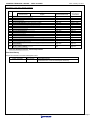
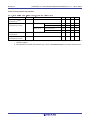
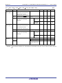
Product
Category
Title
MPU/MCU
Document
No.
TN-RL*-A016A/E
Correction for Incorrect Description Notice RL78/L12
Descriptions in the User’s Manual: Hardware Rev. 1.00
Changed
Information
Category
Technical Notification
Reference
Document
RL78/L12 User’s Manual: Hardware
Rev. 1.00
R01UH0330EJ0100 (Jan. 2013)
Rev.
1.00
Lot No.
Applicable
Product
RL78/L12 Group
R5F10Rxxx
All lots
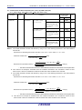
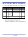
This document describes misstatements found in the RL78/L12 User’s Manual: Hardware Rev. 1.00 (R01UH0330EJ0100).
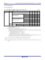
Corrections
Applicable Item
Applicable Page
Contents
3.1.3 Internal data memory space
Page 60
Specifications extended
12.6.3 SNOOZE mode function
Page 490
Specifications changed
19.3.2 STOP mode
Pages 746, 747
Incorrect descriptions revised
19.3.3 SNOOZE mode
Page 749
Incorrect descriptions revised
23.3.6 Invalid memory access detection function
Page 797
Incorrect descriptions revised
Figure 25-3 Format of Option Byte (000C2H)
Page 810
Specifications extended
26.4.3 Procedure for accessing data flash memory
Page 823
Incorrect descriptions revised
30.3.1 Pin characteristics
Pages 867, 868
Incorrect descriptions revised
30.3.2 Supply current characteristics
Pages 872 to 877
Incorrect descriptions revised
30.4 AC Characteristics
Page 878
Specifications extended
30.5.1 Serial array unit
Pages 881 to 899
Incorrect descriptions revised
30.5.2 Serial interface IICA
Pages 900 to 902
Incorrect descriptions revised
30.6.1 A/D converter characteristics
Pages 903 to 905
Specifications extended
30.6.2 Temperature sensor/internal reference voltage
characteristics
Page 905
Incorrect descriptions revised
30.6.3 POR circuit characteristics
Page 905
Incorrect descriptions revised
30.6.5 Supply voltage rise time
Page 907
Specifications added
30.7 Data Memory STOP Mode Low Supply Voltage
Data Retention Characteristics
Page 912
Specifications extended
ELECTRICAL SPECIFICATIONS
(G: TA = −40 to +105°C)
New
Specifications extended
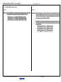
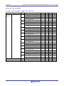
Document Improvement
The above corrections will be made for the next revision of the User’s Manual: Hardware.
(c) 2014. Renesas Electronics Corporation. All rights reserved.
Page 1 of 14
Date: January 10, 2014
RENESAS TECHNICAL UPDATE TN-RL*-A016A/E
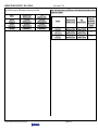
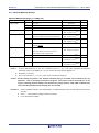
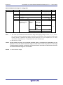
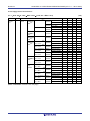
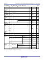
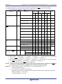
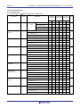
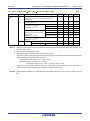
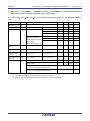
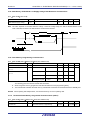
Corrections in the User’s Manual: Hardware
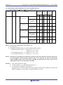
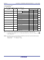
Corrections and Applicable Items
No.
1
2
3
4
5
6
7
8
9
10
11
12
13
14
15
16
17
18
Document No.
English
3.1.3 Internal data memory space
12.6.3 SNOOZE mode function
19.3.2 STOP mode
19.3.3 SNOOZE mode
23.3.6 Invalid memory access detection function
Figure 25-3 Format of Option Byte (000C2H)
26.4.3 Procedure for accessing data flash memory
30.3.1 Pin characteristics
30.3.2 Supply current characteristics
30.4 AC Characteristics
30.5.1 Serial array unit
30.5.2 Serial interface IICA
30.6.1 A/D converter characteristics
30.6.2 Temperature sensor/internal reference voltage characteristics
30.6.3 POR circuit characteristics
30.6.5 Supply voltage rise time
30.7 Data Memory STOP Mode Low Supply Voltage Data Retention
Characteristics
ELECTRICAL SPECIFICATIONS
(G: TA = −40 to +105°C)
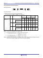
Page 60
Page 490
Pages 746, 747
Page 749
Page 797
Page 810
Page 823
Pages 867, 868
Pages 872 to 877
Page 878
Pages 881 to 899
Pages 900 to 902
Pages 903 to 905
Page 905
Page 905
Page 907
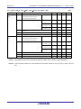
Pages in this
document for
corrections
Page 3
Pages 4 and 5
Page 6
Page 7
Pages 8 and 9
Page 10
Page 11,12
Page 13
Page 13
Page 13
Page 13
Page 13
Page 13
Page 14
Page 14
Page 14
Page 912
Page 14
New
Page 14
R01UH0330EJ0100
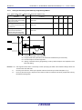
Incorrect: Bold with underline; Correct: Gray hatched
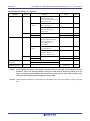
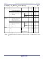
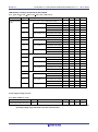
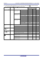
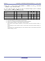
Revision History
RL78/L12 Correction for incorrect description notice
Document Number
TN-RL*-A016A/E
Issue Date
Jan.10.2014
(c) 2014. Renesas Electronics Corporation. All rights reserved.
Description
First edition issued
Corrections No.1 to No.18 revised (This document)
Page 2
RENESAS TECHNICAL UPDATE TN-RL*-A016A/E
Date: Januay 10, 2014
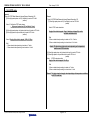
1. 3.1.3 Internal data memory space
Incorrect:
Correct:
Cautions 2. The internal RAM in the following products cannot be used as stack area
when using the self-programming function and data flash function.
Cautions 2. While self-programming is being executed or rewriting the data flash, do not
allocate the RAM address which is used in stack, data buffer, the branch of
vectored interrupt servicing, or the transfer destination or source by DTC
in the address between FFE20H to FFEDFH.
R5F10Rx8 (x = B, F, G, J): FFE20H to FFEDFH, FFB00H to FFC89H
R5F10RxA (x = B, F, G, J, L): FFE20H to FFEDFH, FFB00H to FFC89H
R5F10RxC (x = B, F, G, J, L): FFE20H to FFEDFH, FF900H to FFC89H
3. The RAM area in the products listed below cannot be used when using the
self-programming function or rewriting the data flash, because they are
used by libraries.
R5F10Rx8(x = B, F, G,J)
:FFB00H to FFC89H
R5F10RxA(x = B, F, G,J, L) :FFB00H to FFC89H
R5F10RxC(x = B, F, G,J, L) :FF900H to FFC89H
(c) 2014. Renesas Electronics Corporation. All rights reserved.
Page 3 of 14
RENESAS TECHNICAL UPDATE TN-RL*-A016A/E
Date: Januay 10, 2014
2. 12.6.3 SNOOZE mode function
Incorrect:
SNOOZE mode makes UART operate reception by RxDq pin input detection while the STOP
mode. Normally UART stops communication in the STOP mode. But, using the SNOOZE
mode makes reception UART operate unless the CPU operation by detecting RxDq pin input.
Correct:
SNOOZE mode makes UART operate reception by RxDq pin input detection while the STOP
mode. Normally UART stops communication in the STOP mode. But, using the SNOOZE
mode makes reception UART operate unless the CPU operation by detecting RxDq pin input.
When using the SNOOZE mode function, set the SWCm bit of serial standby control register m
(SSCm) to 1 just before switching to the STOP mode.
When using UARTq in SNOOZE mode, execute the following settings before entering
STOP mode (Refer to Flowcharts of SNOOZE mode operation in Figure 12-93 and
Figure 12-95).
•
In SNOOZE mode, UART reception baud rate must be set differently from normal
operation. Refer to Table 12-3 to set registers SPSm and SDRmn [15:9].
•
Set bits EOCmn and SSECmn to enable or disable the error interrupt (INTSRE0)
when a communication error occurs.
•
Set the SWCm bit in the serial standby control register m (SSCm) to 1 just before
entering STOP mode. After initialization, set the SSm1 bit to 1 in the serial channel
start register m (SSm).
Cautions: 1. The SNOOZE mode can only be specified when the high-speed on-chip oscillator
clock is selected for fCLK.
2. The maximum transfer rate when using UARTq in the SNOOZE mode is
9600 bps.
When the MCU detects the RxDq pin edge input (input the start bit) after entering STOP
mode, the UART reception is started.
Cautions: 1. The SNOOZE mode can only be specified when the high-speed on-chip oscillator
clock (fIH) is selected for fCLK.
2. The transfer rate in SNOOZE mode is 4800 bps only.
3. When the SWCm bit is 1, UARTq can be used only when the reception is
started in STOP mode. If UARTq is used with other SNOOZE function or
interrupts concurrently and the reception is started in state other than
STOP mode as described below, the UARTq cannot receive data correctly
and may cause a framing error or parity error.
•The case the UARTq reception is started from the moment the SWCm bit is
set to 0 before the MCU enters STOP mode
•The case the UARTq reception is started in SNOOZE mode
•The case the UARTq reception is started from the moment the MCU exits
STOP mode and enters normal mode using interrupts before the SWCm bit
is set to 0
(c) 2014. Renesas Electronics Corporation. All rights reserved.
Page 4 of 14
RENESAS TECHNICAL UPDATE TN-RL*-A016A/E
Date: Januay 10, 2014
4. When the SSECm bit is 1, if a parity error, framing error, or overrun error
occurs, flags PEFmn, FEFmn, or OVFmn is not set, nor an error interrupt
(INTSREq) is generated. To set the SSECm bit to 1, clear flags PEFmn,
FEFmn, and OVFmn before setting the SWC0 bit to 1, and read bits 7 to 0
(RxDq) in the SDRm1 register.
Table 12-3 UART Reception Baud Rate Setting in SNOOZE Mode
High-speed on-chip
oscillator
UART reception baud rate in SNOOZE mode
(fIH)
Baud rate: 4800 bps
Operating clock
(fMCK)
SDRmn
[15:9]
Maximum
acceptable value
Minimum
acceptable value
24 MHz ± 1.0% (note)
fCLK /25
79
1.60%
−2.18%
(note)
fCLK /24
105
2.27%
−1.53%
12 MHz ± 1.0% (note)
fCLK /24
79
1.60%
−2.19%
8 MHz ± 1.0% (note)
fCLK /23
105
2.27%
−1.53%
(note)
3
16 MHz ± 1.0%
fCLK /2
79
1.60%
−2.19%
4 MHz ± 1.0% (note)
fCLK /22
105
2.27%
−1.53%
3 MHz ± 1.0% (note)
fCLK /22
79
1.60%
−2.19%
2 MHz ± 1.0% (note)
fCLK /21
105
2.27%
−1.54%
1 MHz ± 1.0% (note)
fCLK /20
105
2.27%
−1.57%
6 MHz ± 1.0%
Note:
When the high-speed on-chip oscillator clock accuracy is at ± 1.5% or 2.0%,
the acceptable range is limited as follows:
• fIH ± 1.5%: Subtract 0.5% from the maximum acceptable value of fIH ± 1.0%,
and add 0.5% to the minimum acceptable value of fIH ± 1.0%.
• fIH ± 2.0%: Subtract 1.0% from the maximum acceptable value of fIH ± 1.0%,
and add 1.0% to the minimum acceptable value of fIH ± 1.0%.
Remarks: Maximum and minimum acceptable values in the above table are the baud
rate acceptable values in UART reception. Make sure to set the baud rate for
transmission within this range.
(c) 2014. Renesas Electronics Corporation. All rights reserved.
Page 5 of 14
RENESAS TECHNICAL UPDATE TN-RL*-A016A/E
Date: Januay 10, 2014
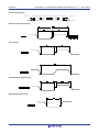
3. 19.3.2 STOP mode
Incorrect:
Figure 19-5 STOP Mode Release by Interrupt Request Generation (1/2)
(1) When high-speed system clock (X1 oscillation) is used as CPU clock
(omitted)
Notes: 2. Wait time for STOP mode release
• High-speed system clock (X1 oscillation): 3-clock
(2) When high-speed system clock (external clock input) is used as CPU clock
(3) When high-speed on-chip oscillator clock is used as CPU clock
(omitted)
Notes: 2.Supply of the clock is stopped: 19.08 to 32.99 µs
Wait
• When vectored interrupt servicing is carried out: 7 clocks
• When vectored interrupt servicing is not carried out: 1 clock
Correct:
Figure 19-5 STOP Mode Release by Interrupt Request Generation (1/2)
(1) When high-speed system clock (X1 oscillation) is used as CPU clock
(omitted)
Notes:2. STOP mode release time
Supply of the clock is stopped: 18 µs to “whichever is longer 65 µs or the
oscillation stabilization time”
Wait
• When vectored interrupt servicing is carried out: 10 to 11 clocks
• When vectored interrupt servicing is not carried out: 4 to 5 clocks
Remark: The time to stop clock supply varies depending on the temperature
conditions and STOP mode time.
(2) When high-speed system clock (external clock input) is used as CPU clock
(3) When high-speed on-chip oscillator clock is used as CPU clock
(omitted)
Notes: 2. STOP mode release time
Supply of the clock is stopped: 18 to 65 µs
Wait
• When vectored interrupt servicing is carried out: 7 clocks
• When vectored interrupt servicing is not carried out: 1 clock
Remark: The time to stop clock supply varies depending on the temperature conditions
and STOP mode time.
(c) 2014. Renesas Electronics Corporation. All rights reserved.
Page 6 of 14
Date: Januay 10, 2014
RENESAS TECHNICAL UPDATE TN-RL*-A016A/E
4. 19.3.3 SNOOZE mode
Incorrect:
In SNOOZE mode transition, wait status to be only following time.
Correct:
The MCU transits from STOP mode to SNOOZE mode or from SNOOZE mode to
normal operation after time shown below elapses.
From STOP to SNOOZE
HS (High-speed main) mode: 18.96 to 28.95 µs
LS (Low-speed main) mode: 20.24 to 28.95µs
LV (Low-voltage main) mode: 20.98 to 28.95 µs
From SNOOZE to normal operation
•
When vectored interrupt servicing is carried out:
HS (High-speed main) mode: 6.79 to 12.4 µs + 7 clocks
LS (Low-speed main) mode: 2.58 to 7.8 µs + 7 clocks
LV (Low-voltage main) mode: 12.45 to 17.3 µs + 7 clocks
•
When vectored interrupt servicing is not carried out:
HS (High-speed main) mode: 6.79 to 12.4 µs + 1 clock
LS (Low-speed main) mode: 2.58 to 7.8 µs + 1 clock
LV (Low-voltage main) mode: 12.45 to 17.3 µs + 1 clock
(c) 2014. Renesas Electronics Corporation. All rights reserved.
Transit time from STOP mode to SNOOZE mode: 18 to 65 µs
Remark: The transit time from STOP mode to SNOOZE mode varies depending on the
temperature conditions and STOP mode time.
Transit time from SNOOZE mode to normal operation:
•
When vectored interrupt servicing is carried out:
HS (High-speed main) mode: “4.99 to 9.44 µs” + 7 clocks
LS (Low-speed main) mode: “1.10 to 5.08 µs” + 7 clocks
LV (Low-voltage main) mode: “16.58 to 25.40 µs” + 7 clocks
•
When vectored interrupt servicing is not carried out:
HS (High-speed main) mode: “4.99 to 9.44 µs” + 1 clock
LS (Low-speed main) mode: “1.10 to 5.08 µs” + 1 clock
LV (Low-voltage main) mode: “16.58 to 25.40 µs” + 1 clock
Page 7 of 14
RENESAS TECHNICAL UPDATE TN-RL*-A016A/E
Date: Januay 10, 2014
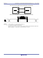
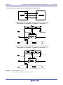
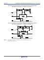
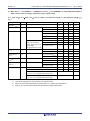
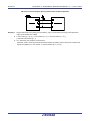
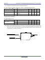
5. 23.3.6 Invalid memory access detection function
Incorrect:
Correct:
Figure 23-10
Invalid access detection area
(c) 2014. Renesas Electronics Corporation. All rights reserved.
Figure 23-10
Invalid access detection area
Page 8 of 14
Date: Januay 10, 2014
RENESAS TECHNICAL UPDATE TN-RL*-A016A/E
Note: Code flash memory and RAM address of each product are as follows.
Products
R5F10Rx8
(x = B, F, G, J)
R5F10RxA
(x = B,F, G, J, L)
R5F10RxC
(x = B, F, G, J, L)
Code flash memory
(00000H to xxxxxH)
8192 × 8 bit
(00000H to 01FFFH)
16384 × 8 bit
(00000H to 03FFFH)
32768 × 8 bit
(00000H to 07FFFH)
(c) 2014. Renesas Electronics Corporation. All rights reserved.
RAM
(yyyyyH to FFEFFH)
1024 × 8 bit
(FFB00H to FFEFFH)
1024 × 8 bit
(FFB00H to FFEFFH)
1536 × 8 bit
(FF900H to FFEFFH)
Note: Code flash memory area, RAM area, and the detected lowest address of each
product are as follows.
Products
Code flash memory
(00000H to xxxxxH)
RAM
(zzzzzH to FFEFFH)
R5F10Rx8
(x = B, F, G, J)
R5F10RxA
(x = B, F, G, J, L)
R5F10Rx8
(x = B, F, G, J)
8192 × 8 bit
(00000H to 01FFFH)
16384 × 8 bit
(00000H to 03FFFH)
8192 × 8 bit
(00000H to 01FFFH)
1024 × 8 bit
(FFB00H to FFEFFH)
1024 × 8 bit
(FFB00H to FFEFFH)
1024 × 8 bit
(FFB00H to FFEFFH)
Page 9 of 14
Detected lowest
address for
read/instruction
fetch (execution)
(yyyyyH)
10000H
10000H
80000H
Date: Januay 10, 2014
RENESAS TECHNICAL UPDATE TN-RL*-A016A/E
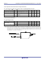
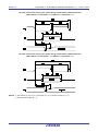
6. Figure 25-3 Format of Option Byte (000C2H)
Old:
Address: 000C2H
New:
Figure 25-3 Format of Option Byte (000C2H)
7
6
CMODE1
C5MODE0
5
4
CMODE1
CMODE0
0
0
LV (low voltage main) mode
1
0
LS (low speed main) mode
1
3
0
2
Address: 000C2H
note
Figure 25-3. Format of Option Byte (000C2H)
1
0
7
6
FRQSEL1
FRQSEL0
CMODE1
C5MODE0
Operating Frequency
Range
Operating Voltage
Range
CMODE1
CMODE0
1 to 4 MHz
1.6 to 5.5 V
0
0
LV (low voltage main) mode
1
0
LS (low speed main) mode
FRQSEL3
FRQSEL2
5
4
1
3
0
Setting of flash operation mode
1
1
Other than above
HS (high speed main) mode
2
FRQSEL3
1 to 8 MHz
1.8 to 5.5 V
1 to 16 MHz
2.4 to 5.5 V
1 to 24 MHz
2.7 to 5.5 V
1
1
Other than above
Frequency of the high-speed on-chip oscillator
Operating Voltage
Range
1 to 4 MHz
1.6 to 5.5 V
HS (high speed main) mode
FRQSEL2
FRQSEL1
FRQSEL0
FRQSEL3
FRQSEL2
FRQSEL1
FRQSEL0
0
0
0
24 MHz
0
0
0
0
24 MHz
1
0
0
1
16 MHz
1
0
0
1
16 MHz
0
0
0
1
12 MHz
0
0
0
1
12 MHz
1
0
1
0
8 MHz
1
0
1
0
8 MHz
1
0
1
1
4 MHz
0
0
1
0
6 MHz
1
1
0
1
1 MHz
1
0
1
1
4 MHz
Setting prohibited
0
0
1
1
3 MHz
1
1
0
1
2 MHz
1
1
0
1
1 MHz
Other than above
Caution:
(c) 2014. Renesas Electronics Corporation. All rights reserved.
1 to 8 MHz
1.8 to 5.5 V
1 to 16 MHz
2.4 to 5.5 V
1 to 24 MHz
2.7 to 5.5 V
Setting prohibited
0
Be sure to set 10B to bits 5 and 4.
0
FRQSEL0
Operating Frequency
Range
FRQSEL3
Caution:
1
FRQSEL1
Setting of flash operation mode
Setting prohibited
Other than above
FRQSEL2
Be sure to set 10B to bits 5 and 4.
Page 10 of 14
Frequency of the high-speed on-chip oscillator
Setting prohibited
RENESAS TECHNICAL UPDATE TN-RL*-A016A/E
Date: Januay 10, 2014
7. 26.4.3 Procedure for accessing data flash memory
Incorrect:
Correct:
The data flash memory is initially stopped after a reset ends and cannot be accessed (read or
programmed). To
access the memory, perform the following procedure:
The data flash memory is stopped after a reset ends. To access the data flash, make initial
settings according to the
<1> Write 1 to bit 0 (DFLEN) of the data flash control register (DFLCTL).
<2> Wait for the setup to finish for software timer. etc.
The time setup takes differs for each main clock mode.
<Setup time for each main clock mode>
• HS (High-speed main): 5μs
• LS (Low-speed main): 720 ns
• LV (Low-voltage main): 10μs
<3> After the wait, the data flash memory can be accessed.
following procedure.
<1> Set bit 0 (DFLEN) of the data flash control register (DFLCTL) to 1.
<2> Wait for the setup to finish for software timer, etc.
The time setup takes differs for each flash operation mode for the main clock.
<Setup time for each flash operation mode>
• HS (High speed main): 5 μs
• LS (Low speed main): 720 ns
• LV (Low voltage main): 10 μs
<3> After the wait, the data flash memory can be accessed.
Cautions 1. Accessing the data flash memory is not possible during the setup time.
2. Before executing a STOP instruction during the setup time, temporarily clear DFLEN to 0.
Cautions 1. Accessing the data flash memory is not possible during the setup time.
2. Transition to the STOP mode is not possible during the setup time. To enter the
STOP mode during the setup time, clear DFLEN to 0 and then execute the STOP
instruction.
3. The high-speed on-chip oscillator should be kept operating during data flash
rewrite. If it is kept stopping, operate the high-speed on-chip oscillator clock
(HIOSTOP = 0) and execute the data flash library after 30 μs have elapsed.
(c) 2014. Renesas Electronics Corporation. All rights reserved.
Page 11 of 14
RENESAS TECHNICAL UPDATE TN-RL*-A016A/E
Date: Januay 10, 2014
After initialized, the data flash memory can be read by using a CPU instruction or can be
read/written by using a data
flash library.
If the DMA controller operates when the data flash memory is accessed, however, follow
one of these procedures:
(A) Suspending/forcibly terminating DMA transfer
Before reading the data flash memory, suspend DMA transfer of all the channels used.
After setting the DWAITn bit to 1, however, wait at least for the duration of three clocks
(fCLK) before reading the
data flash memory. After reading the data flash memory, lift the suspension of transfer by
clearing the DWAITn bit to 0.
Or, forcibly terminate DMA transfer in accordance with the procedure in 15.5.5 Forced
termination by software
before reading the data flash memory. Resume DMA transfer after the data flash memory
has been read.
(B) Access the data flash memory by using the newest data flash library.
(C) Insertion of NOP
Insert an NOP instruction immediately before the instruction that reads the data flash
memory.
<Example>
MOVW HL,!addr16 ; Reads RAM.
NOP ; Insert NOP instruction before reading data flash memory.
MOV A,[DE] ; Read data flash memory.
If a high-level language such as C is used, however, the compiler may generate two
instructions for one code. In
this case, the NOP instruction is not inserted immediately before the data flash memory read
instruction.
Therefore, read the data flash memory by (A) or (B) above.
Remarks 1. n: DMA channel number (n = 0, 1)
2. fCLK: CPU/peripheral hardware clock frequency
(c) 2014. Renesas Electronics Corporation. All rights reserved.
Page 12 of 14
RENESAS TECHNICAL UPDATE TN-RL*-A016A/E
Date: Januay 10, 2014
8. 30.3.1 Pin characteristics
Incorrect:
Fixed typo in Note 2 in pages 867 and 868.
Correct:
Refer to pages 7 and 8 in Technical Update Exhibit 1 “Chapter 30 ELECTRICAL
SPECIFICATIONS”.
9. 30.3.2 Supply current characteristics
Incorrect:
Fixed typo in Notes and typical values of IDD2 and IDD3 in pages 872 to 877.
Correct:
Refer to pages 12 to 17 in Technical Update Exhibit 1 “Chapter 30 ELECTRICAL
SPECIFICATIONS”.
10. 30.4 AC Characteristics
Old:
Specifications of the external system clock frequency and external system clock input
high-level width, low-level width in page 878 extended.
New:
Refer to page 18 in Technical Update Exhibit 1 “Chapter 30 ELECTRICAL SPECIFICATIONS”.
11. 30.5.1 Serial array unit
Incorrect:
Fixed typo in 30.5.1 Serial array unit in pages 881 to 899.
Correct:
Refer to pages 24 to 44 in Technical Update Exhibit 1 “Chapter 30 ELECTRICAL
SPECIFICATIONS”.
12. 30.5.2 Serial interface IICA
Incorrect:
Fixed typo in 30.5.2 Serial interface IICA in pages 900 to 902.
Correct:
Refer to pages 45 to 49 in Technical Update Exhibit 1 “Chapter 30 ELECTRICAL
SPECIFICATIONS”.
13. 30.6.1 A/D converter characteristics
New:
Old:
Specifications in 30.6.1 A/D converter characteristics in pages 903 to 905 extended.
(c) 2014. Renesas Electronics Corporation. All rights reserved.
Refer to pages 50 to 53 in Technical Update Exhibit 1 “Chapter 30 ELECTRICAL
SPECIFICATIONS”.
Page 13 of 14
RENESAS TECHNICAL UPDATE TN-RL*-A016A/E
Date: Januay 10, 2014
14. 30.6.2 Temperature sensor/internal reference voltage characteristics
Incorrect:
Fixed typo in 30.6.2 Temperature Sensor/Internal Reference Voltage Characteristics in page
905.
Correct:
Refer to page 54 in Technical Update Exhibit 1 “Chapter 30 ELECTRICAL SPECIFICATIONS”.
15. 30.6.3 POR circuit characteristics
Incorrect:
Fixed typo in 30.6.3 POR circuit characteristics in page 905.
Correct:
Refer to page 54 in Technical Update Exhibit 1 “Chapter 30 ELECTRICAL SPECIFICATIONS”.
16. 30.6.5 Supply voltage rise time
Old:
Specifications in Supply Voltage Rise Time in page 907 added.
New:
Refer to page 56 in Technical Update Exhibit 1 “Chapter 30 ELECTRICAL SPECIFICATIONS”.
17. 30.8 Data Memory STOP Mode Low Supply Voltage Data Retention
Characteristics
Old:
Specifications in Data Memory STOP Mode Low Supply Voltage Data Retention
Characteristics in page 912 extended.
New:
Refer to page 61 in Technical Update Exhibit 1 “Chapter 30 ELECTRICAL SPECIFICATIONS
(A, D: TA = −40 to + 85°C)”.
18. ELECTRICAL SPECIFICATIONS (G: TA = −40 to +105°C)
Old:
Specifications in ELECTRICAL SPECIFICATIONS (G: TA = −40 to +105°C) extended.
(c) 2014. Renesas Electronics Corporation. All rights reserved.
New:
Refer to Technical Update Exhibit 2 “Chapter 31 ELECTRICAL SPECIFICATIONS”.
Page 14 of 14
RL78/L12
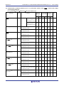
CHAPTER 30 ELECTRICAL SPECIFICATIONS (A,G: TA = −40 to +85°C)
CHAPTER 30 ELECTRICAL SPECIFICATIONS
This chapter describes the electrical specifications for the products "A: Consumer applications (TA = −40 to +85°C)", and
"G: Industrial applications (TA when using the RL78 microcontrollers at −40 to +85°C)".
Cautions 1. The RL78 microcontrollers have an on-chip debug function, which is provided for development and
evaluation. Do not use the on-chip debug function in products designated for mass production,
because the guaranteed number of rewritable times of the flash memory may be exceeded when
this function is used, and product reliability therefore cannot be guaranteed.
Renesas
Electronics is not liable for problems occurring when the on-chip debug function is used.
2. With products not provided with an EVDD, or EVSS pin, replace EVDD with VDD, or replace EVSS with
VSS.
3. The pins mounted depend on the product. Refer to 2.1 Port Function to 2.1.6 Pins for each
product (pins other than port pins).
1
RL78/L12
CHAPTER 30 ELECTRICAL SPECIFICATIONS (A,G: TA = −40 to +85°C)
30.1 Absolute Maximum Ratings
Absolute Maximum Ratings (TA = 25°C) (1/3)
Parameter
Symbols
Supply voltage
Conditions
Ratings
Unit
VDD
VDD = EVDD
−0.5 to +6.5
V
EVDD
VDD = EVDD
−0.5 to +6.5
V
−0.5 to +0.3
V
EVSS
REGC pin input voltage VIREGC
REGC
−0.3 to +2.8
and −0.3 to VDD +0.3 Note 1
V
Input voltage
VI1
P10 to P17, P30 to P32, P40 to P43, P50 to P54,
P70 to P74, P120, P125 to P127,P140 to P147
−0.3 to EVDD +0.3
and −0.3 to VDD +0.3 Note 2
V
VI2
P60, P61 (N-ch open-drain)
−0.3 to EVDD +0.3
and −0.3 to VDD +0.3 Note 2
V
VI3
P20, P21, P121 to P124, P137, EXCLK,
−0.3 to VDD +0.3 Note 2
V
−0.3 to EVDD +0.3
and −0.3 to VDD +0.3 Note 2
V
−0.3 to VDD +0.3 Note 2
V
EXCLKS, RESET
Output voltage
VO1
P10 to P17, P30 to P32, P40 to P43,
P50 to P54, P60, P61, P70 to P74, P120,
P125 to P127, P130, P140 to P147
Analog input voltage
Notes 1.
VO2
P20, P21
VAI1
ANI16 to ANI23
−0.3 to EVDD +0.3 and
−0.3 to AVREF(+) +0.3 Notes 2, 3
V
VAI2
ANI0, ANI1
−0.3 to VDD +0.3 and
−0.3 to AVREF(+) +0.3 Notes 2, 3
V
Connect the REGC pin to Vss via a capacitor (0.47 to 1 µF). This value regulates the absolute
maximum rating of the REGC pin. Do not use this pin with voltage applied to it.
2.
Must be 6.5 V or lower.
3.
Do not exceed AVREF(+) + 0.3 V in case of A/D conversion target pin.
Caution Product quality may suffer if the absolute maximum rating is exceeded even momentarily for any
parameter. That is, the absolute maximum ratings are rated values at which the product is on the
verge of suffering physical damage, and therefore the product must be used under conditions that
ensure that the absolute maximum ratings are not exceeded.
Remarks 1.
Unless specified otherwise, the characteristics of alternate-function pins are the same as those of the
port pins.
2.
AVREF(+) : + side reference voltage of the A/D converter.
3.
VSS is the reference voltage.
2
RL78/L12
CHAPTER 30 ELECTRICAL SPECIFICATIONS (A,G: TA = −40 to +85°C)
Absolute Maximum Ratings (TA = 25°C) (2/3)
Parameter
LCD voltage
Notes
Symbols
Conditions
Ratings
Unit
−0.3 to +2.8 and
−0.3 to VL4 +0.3
V
VL1
VL1 voltage
VL2
VL2 voltageNote 1
−0.3 to VL4 +0.3 Note 2
V
VL3
VL3 voltageNote 1
−0.3 to VL4 +0.3 Note 2
V
VL4
VL4 voltage
−0.3 to +6.5
V
VLCAP
CAPL, CAPH voltage
VLOUT
COM0 to COM7, SEG0
to SEG38, COMEXP
output voltage
Note 1
Note 1
−0.3 to VL4 +0.3
Note 2
Other than
memory-type
liquid crystal
mode
−0.3 to VDD +0.3
Note 2
Memory-type
liquid crystal
mode
−0.3 to VL4 +0.3 Note 2
Note 1
External
resistance
division
Capacitor split
−0.3 to VDD +0.3 Note 2
Internal voltage boosting
−0.3 to VL4 +0.3 Note 2
V
V
1. This value only indicates the absolute maximum ratings when applying voltage to the VL1, VL2, VL3, and VL4
pins; it does not mean that applying voltage to these pins is recommended. When using the internal voltage
boosting method or capacitance split method, connect these pins to VSS via a capacitor (0.47 µF ± 30%)
and connect a capacitor (0.47 µF ± 30%) between the CAPL and CAPH pins.
2. Must be 6.5 V or lower.
Caution Product quality may suffer if the absolute maximum rating is exceeded even momentarily for any
parameter. That is, the absolute maximum ratings are rated values at which the product is on the verge
of suffering physical damage, and therefore the product must be used under conditions that ensure that
the absolute maximum ratings are not exceeded.
Remark VSS is the reference voltage.
3
RL78/L12
CHAPTER 30 ELECTRICAL SPECIFICATIONS (A,G: TA = −40 to +85°C)
Absolute Maximum Ratings (TA = 25°C) (3/3)
Parameter
Output current, high
Symbols
IOH1
Conditions
Ratings
Unit
Per pin
P10 to P17, P30 to P32,
P40 to P43, P50 to P54,
P70 to P74, P120, P125 to P127,
P130, P140 to P147
−40
mA
Total of all pins
−170 mA
P10 to P14, P40 to P43, P120,
P130, P140 to P147
−70
mA
P15 to P17, P30 to P32,
−100
mA
−0.5
mA
−1
mA
P50 to P54, P70 to P74,
P125 to P127
IOH2
Per pin
P20, P21
Total of all pins
Output current, low
IOL1
IOL2
Per pin
P10 to P17, P30 to P32,
P40 to P43, P50 to P54, P60,
P61, P70 to P74, P120,
P125 to P127, P130,
P140 to P147
40
mA
Total of all pins
170 mA
P10 to P14, P40 to P43, P120,
P130, P140 to P147
70
mA
P15 to P17, P30 to P32,
P50 to P54, P60, P61,
P70 to P74, P125 to P127
100
mA
1
mA
2
mA
−40 to +85
°C
−65 to +150
°C
Per pin
P20, P21
Total of all pins
Operating ambient
temperature
TA
Storage temperature
Tstg
In normal operation mode
In flash memory programming mode
Caution Product quality may suffer if the absolute maximum rating is exceeded even momentarily for any
parameter. That is, the absolute maximum ratings are rated values at which the product is on the
verge of suffering physical damage, and therefore the product must be used under conditions that
ensure that the absolute maximum ratings are not exceeded.
Remark Unless specified otherwise, the characteristics of alternate-function pins are the same as those of the port
pins.
4
RL78/L12
CHAPTER 30 ELECTRICAL SPECIFICATIONS (A,G: TA = −40 to +85°C)
30.2 Oscillator Characteristics
30.2.1 X1, XT1 oscillator characteristics
(TA = −40 to +85°C, 1.6 V ≤ EVDD = VDD ≤ 5.5 V, VSS = EVSS = 0 V)
Parameter
X1 clock oscillation
frequency (fX) Note
XT1 clock oscillation
frequency (fXT) Note
Resonator
Ceramic resonator/
crystal resonator
Conditions
MIN.
TYP.
MAX.
2.7 V ≤ VDD ≤ 5.5 V
1.0
20.0
2.4 V ≤ VDD ≤ 2.7 V
1.0
16.0
1.8 V ≤ VDD < 2.7 V
1.0
8.0
1.6 V ≤ VDD <1.8 V
1.0
4.0
Crystal resonator
32
32.768
35
Unit
MHz
kHz
Note Indicates only the permissible deviation of the oscillator frequencies. Refer to AC Characteristics for instruction
execution time. Inquire with the resonator manufacturer to perform an evaluation on the actual circuit and check
the oscillator characteristics before use.
Caution Since the CPU is started by the high-speed on-chip oscillator clock after a reset release, check the X1
clock oscillation stabilization time using the oscillation stabilization time counter status register
(OSTC) by the user. Determine the oscillation stabilization time of the OSTC register and the
oscillation stabilization time select register (OSTS) after sufficiently evaluating the oscillation
stabilization time with the resonator to be used.
Remark
When using the X1 or XT1 oscillator, refer to 5.4 System Clock Oscillator.
5
RL78/L12
CHAPTER 30 ELECTRICAL SPECIFICATIONS (A,G: TA = −40 to +85°C)
30.2.2 On-chip oscillator characteristics
(TA = −40 to +85°C, 1.6 V ≤ EVDD = VDD ≤ 5.5 V, VSS = EVSS = 0 V)
Oscillators
High-speed on-chip oscillator
clock frequency Notes 1, 2
Parameters
Conditions
High-speed on-chip oscillator
clock frequency accuracy
−20 to +85 °C
−40 to −20 °C
Low-speed on-chip oscillator
clock frequency
MAX.
Unit
1
24
MHz
1.8 V ≤ VDD ≤ 5.5 V
−1
+1
%
1.6 V ≤ VDD ≤ 1.8 V
−5
+5
%
1.8 V ≤ VDD ≤ 5.5 V
−1.5
+1.5
%
1.6 V ≤ VDD ≤1.8 V
−5.5
+5.5
%
fIH
MIN.
fIL
Low-speed on-chip oscillator
clock frequency accuracy
TYP.
15
−15
kHz
+15
%
Notes 1. High-speed on-chip oscillator frequency is selected by bits 0 to 3 of option byte (000C2H) and bits 0 to 2 of
HOCODIV register.
2. This indicates the oscillator characteristics only. Refer to AC Characteristics for instruction execution time.
6
RL78/L12
CHAPTER 30 ELECTRICAL SPECIFICATIONS (A,G: TA = −40 to +85°C)
30.3 DC Characteristics
30.3.1 Pin characteristics
(TA = −40 to +85°C, 1.6 V ≤ EVDD = VDD ≤ 5.5 V, VSS = EVSS = 0 V)
Items
Symbol
Output current,
highNote 1
IOH1
Conditions
(1/5)
MIN.
Per pin for P10 to P17, P30 to P32, P40 to P43, P50 to P54,
P70 to P74, P120, P125 to P127, P130, P140 to P147
Unit
−10.0
mA
Note 2
4.0 V ≤ EVDD ≤ 5.5 V
−40.0
mA
2.7 V ≤ EVDD < 4.0 V
−8.0
mA
1.8 V ≤ EVDD < 2.7 V
−4.0
mA
1.6 V ≤ EVDD < 1.8 V
−2.0
mA
Total of P15 to P17, P30 to P32,
P50 to P54, P70 to P74, P125 to P127
(When duty = 70% Note 3)
4.0 V ≤ EVDD ≤ 5.5 V
−60.0
mA
2.7 V ≤ EVDD < 4.0 V
−15.0
mA
1.8 V ≤ EVDD < 2.7 V
−8.0
mA
1.6 V ≤ EVDD < 1.8 V
−4.0
mA
−100.0
mA
−0.1
mA
−0.2
mA
Total of all pins (When duty = 70%
)
P20, P21
Per pin
Total of all pins
Notes 1.
MAX.
Total of P10 to P14, P40 to P43, P120,
P130, P140 to P147
(When duty = 70% Note 3)
Note 3
IOH2
TYP.
1.6 V ≤ VDD ≤ 5.5 V
Value of current at which the device operation is guaranteed even if the current flows from the VDD, EVDD
pins to an output pin.
2.
Do not exceed the total current value.
3.
Specification under conditions where the duty factor is 70%.
The output current value that has changed the duty ratio can be calculated with the following expression
(when changing the duty factor from 70% to n%).
• Total output current of pins = (IOH × 0.7)/(n × 0.01)
<Example> Where n = 80% and IOH = −10.0 mA
Total output current of pins = (−10.0 × 0.7)/(80 × 0.01) ≈ −8.7 mA
However, the current that is allowed to flow into one pin does not vary depending on the duty factor. A
current higher than the absolute maximum rating must not flow into one pin.
Caution P10, P12, P15, P17 do not output high level in N-ch open-drain mode.
Remark Unless specified otherwise, the characteristics of alternate-function pins are the same as those of the port
pins.
7
RL78/L12
CHAPTER 30 ELECTRICAL SPECIFICATIONS (A,G: TA = −40 to +85°C)
(TA = −40 to +85°C, 1.6 V ≤ EVDD = VDD ≤ 5.5 V, VSS = EVSS = 0 V)
Items
Symbol
Output current,
lowNote 1
IOL1
Conditions
(2/5)
MIN.
Per pin for P10 to P17, P30 to P32, P40 to P43,
P50 to P54, P70 to P74, P120, P125 to P127, P130,
P140 to P147
Total of P15 to P17, P30 to P32,
P50 to P54, P60, P61, P70 to P74,
P125 to P127
(When duty = 70% Note 3)
P20, P21
Notes 1.
mA
Note 2
4.0 V ≤ EVDD ≤ 5.5 V
70.0
mA
2.7 V ≤ EVDD < 4.0 V
15.0
mA
1.8 V ≤ EVDD < 2.7 V
9.0
mA
1.6 V ≤ EVDD < 1.8 V
4.5
mA
4.0 V ≤ EVDD ≤ 5.5 V
80.0
mA
2.7 V ≤ EVDD < 4.0 V
35.0
mA
1.8 V ≤ EVDD < 2.7 V
20.0
mA
1.6 V ≤ EVDD < 1.8 V
10.0
mA
150.0
mA
0.4
mA
0.8
mA
Per pin
Total of all pins
Unit
20.0
mA
Total of all pins
(When duty = 70% Note 3)
IOL2
MAX.
15.0 Note 2
Per pin for P60, P61
Total of P10 to P14, P40 to P43,
P120, P130, P140 to P147
(When duty = 70% Note 3)
TYP.
1.6 V ≤ VDD ≤ 5.5 V
Value of current at which the device operation is guaranteed even if the current flows from an output pin to
the EVSS and VSS pin.
2.
3.
Do not exceed the total current value.
Specification under conditions where the duty factor is 70%.
The output current value that has changed the duty ratio can be calculated with the following expression
(when changing the duty factor from 70% to n%).
• Total output current of pins = (IOL × 0.7)/(n × 0.01)
<Example> Where n = 80% and IOL = 10.0 mA
Total output current of pins = (10.0 × 0.7)/(80 × 0.01) ≈ 8.7 mA
However, the current that is allowed to flow into one pin does not vary depending on the duty factor. A
current higher than the absolute maximum rating must not flow into one pin.
Remark Unless specified otherwise, the characteristics of alternate-function pins are the same as those of the port
pins.
8
RL78/L12
CHAPTER 30 ELECTRICAL SPECIFICATIONS (A,G: TA = −40 to +85°C)
(TA = −40 to +85°C, 1.6 V ≤ EVDD = VDD ≤ 5.5 V, VSS = EVSS = 0 V)
Items
Input voltage,
high
Input voltage,
low
Symbol
Conditions
(3/5)
MIN.
TYP.
MAX.
Unit
VIH1
P10 to P17, P30 to P32, P40 to P43,
P50 to P54, P70 to P74, P120,
P125 to P127, P140 to P147
Normal input buffer 0.8EVDD
EVDD
V
VIH2
P10, P11, P15, P16
TTL input buffer
4.0 V ≤ EVDD ≤ 5.5 V
2.2
EVDD
V
TTL input buffer
3.3 V ≤ EVDD < 4.0 V
2.0
EVDD
V
TTL input buffer
1.6 V ≤ EVDD < 3.3 V
1.50
EVDD
V
VIH3
P20, P21
0.7VDD
VDD
V
VIH4
P60, P61
0.7EVDD
EVDD
V
VIH5
P121 to P124, P137, EXCLK, EXCLKS, RESET
0.8VDD
VDD
V
VIL1
P10 to P17, P30 to P32, P40 to P43,
P50 to P54, P70 to P74, P120,
P125 to P127, P140 to P147
Normal input buffer
0
0.2EVDD
V
VIL2
P10, P11, P15, P16
TTL input buffer
4.0 V ≤ EVDD ≤ 5.5 V
0
0.8
V
TTL input buffer
3.3 V ≤ EVDD < 4.0 V
0
0.5
V
TTL input buffer
1.6 V ≤ EVDD < 3.3 V
0
0.32
V
VIL3
P20, P21
0
0.3VDD
V
VIL4
P60, P61
0
0.3EVDD
V
VIL5
P121 to P124, P137, EXCLK, EXCLKS, RESET
0
0.2VDD
V
Caution The maximum value of VIH of P10, P12, P15, P17 is EVDD, even in the N-ch open-drain mode.
Remark Unless specified otherwise, the characteristics of alternate-function pins are the same as those of the port
pins.
9
RL78/L12
CHAPTER 30 ELECTRICAL SPECIFICATIONS (A,G: TA = −40 to +85°C)
(TA = −40 to +85°C, 1.6 V ≤ EVDD = VDD ≤ 5.5 V, VSS = EVSS = 0 V)
Items
Symbol
Output voltage,
high
Output voltage,
low
VOH1
Conditions
P10 to P17, P30 to P32, P40 to P43,
P50 to P54, P70 to P74, P120,
P125 to P127, P130, P140 to P147
(4/5)
MIN.
TYP.
MAX.
Unit
4.0 V ≤ EVDD ≤ 5.5 V, EVDD−1.5
IOH1 = −10 mA
V
4.0 V ≤ EVDD ≤ 5.5 V, EVDD−0.7
IOH1 = −3.0 mA
V
2.7 V ≤ EVDD ≤ 5.5 V, EVDD−0.6
IOH1 = −2.0 mA
V
1.8 V ≤ EVDD ≤ 5.5 V, EVDD−0.5
IOH1 = −1.5 mA
V
1.6 V ≤ EVDD < 5.5 V, EVDD−0.5
IOH1 = −1.0 mA
V
V
VOH2
P20, P21
1.6 V ≤ VDD ≤ 5.5 V,
IOH2 = −100 µ A
VDD−0.5
VOL1
P10 to P17, P30 to P32, P40 to P43,
P50 to P54, P70 to P74, P120,
P125 to P127, P130, P140 to P147
4.0 V ≤ EVDD ≤ 5.5 V,
IOL1 = 20 mA
1.3
V
4.0 V ≤ EVDD ≤ 5.5 V,
IOL1 = 8.5 mA
0.7
V
2.7 V ≤ EVDD ≤ 5.5 V,
IOL1 = 3.0 mA
0.6
V
2.7 V ≤ EVDD ≤ 5.5 V,
IOL1 = 1.5 mA
0.4
V
1.8 V ≤ EVDD ≤ 5.5 V,
IOL1 = 0.6 mA
0.4
V
1.6 V ≤ EVDD < 5.5 V,
IOL1 = 0.3 mA
0.4
V
VOL2
P20, P21
1.6 V ≤ VDD ≤ 5.5 V,
IOL2 = 400 µ A
0.4
V
VOL3
P60, P61
4.0 V ≤ EVDD ≤ 5.5 V,
IOL3 = 15.0 mA
2.0
V
4.0 V ≤ EVDD ≤ 5.5 V,
IOL3 = 5.0 mA
0.4
V
2.7 V ≤ EVDD ≤ 5.5 V,
IOL3 = 3.0 mA
0.4
V
1.8 V ≤ EVDD ≤ 5.5 V,
IOL3 = 2.0 mA
0.4
V
1.6 V ≤ EVDD < 5.5 V,
IOL3 = 1.0 mA
0.4
V
Caution P10, P12, P15, P17 do not output high level in N-ch open-drain mode.
Remark Unless specified otherwise, the characteristics of alternate-function pins are the same as those of the port
pins.
10
RL78/L12
CHAPTER 30 ELECTRICAL SPECIFICATIONS (A,G: TA = −40 to +85°C)
(TA = −40 to +85°C, 1.6 V ≤ EVDD = VDD ≤ 5.5 V, VSS = EVSS = 0 V)
Items
Symbol
Input leakage
current, high
Input leakage
current, low
Conditions
(5/5)
MIN.
TYP.
Unit
ILIH1
P10 to P17, P30 to P32,
P40 to P43, P50 to P54, P60,
P61, P70 to P74, P120,
P125 to P127, P140 to P147
VI = EVDD
1
µA
ILIH2
P20, P21, P137, RESET
VI = VDD
1
µA
ILIH3
P121 to P124
(X1, X2, XT1, XT2, EXCLK,
EXCLKS)
VI = VDD
In input port or
external clock
input
1
µA
In resonator
connection
10
µA
ILIL1
P10 to P17, P30 to P32,
P40 to P43, P50 to P54, P60,
P61, P70 to P74, P120,
P125 to P127, P140 to P147
VI = EVSS
−1
µA
ILIL2
P20, P21, P137, RESET
VI = VSS
−1
µA
P121 to P124
VI = VSS
−1
µA
−10
µA
ILIL3
(X1, X2, XT1, XT2, EXCLK,
EXCLKS)
In input port or
external clock
input
In resonator
connection
On-chip pull-up
resistance
MAX.
RU1
RU2
VI = EVSS
SEGxx port
2.4 V ≤ EVDD = VDD ≤ 5.5 V
10
20
100
kΩ
1.6 V ≤ EVDD = VDD < 2.4 V
10
30
100
kΩ
10
20
100
kΩ
Ports other than above
(Except for P60, P61, and
P130)
Remark Unless specified otherwise, the characteristics of alternate-function pins are the same as those of the port
pins.
11
RL78/L12
CHAPTER 30 ELECTRICAL SPECIFICATIONS (A,G: TA = −40 to +85°C)
30.3.2 Supply current characteristics
(TA = −40 to +85°C, 1.6 V ≤ EVDD = VDD ≤ 5.5 V, VSS = EVSS = 0 V)
Parameter
Symbol
Supply
current
IDD1
Note 1
Conditions
Operating
mode
HS (highspeed main)
mode Note 5
fIH = 24 MHz
MIN.
Note 3
fIH = 16 MHz Note 3
LS (lowspeed main)
mode Note 5
fIH = 8 MHz
(1/3)
MAX.
Unit
Basic
VDD = 5.0 V
operation VDD = 3.0 V
1.5
VDD = 5.0 V
Normal
operation VDD = 3.0 V
3.3
3.3
5.0
mA
Normal
VDD = 5.0 V
operation VDD = 3.0 V
2.5
3.7
mA
2.5
3.7
mA
Normal
VDD = 3.0 V
operation VDD = 2.0 V
Note 3
TYP.
mA
1.5
mA
5.0
mA
1.2
1.8
mA
1.2
1.8
mA
1.2
1.7
mA
1.2
1.7
mA
LV (lowfIH = 4 MHz Note 3
voltage main)
mode Note 5
Normal
VDD = 3.0 V
operation VDD = 2.0 V
HS (highspeed main)
mode Note 5
Normal
Square wave input
operation Resonator connection
2.8
4.4
mA
3.0
4.6
mA
Normal
Square wave input
operation Resonator connection
2.8
4.4
mA
3.0
4.6
mA
Normal
Square wave input
operation Resonator connection
1.8
2.6
mA
1.8
2.6
mA
Normal
Square wave input
operation Resonator connection
1.8
2.6
mA
1.8
2.6
mA
Normal
Square wave input
operation Resonator connection
1.1
1.7
mA
1.1
1.7
mA
Normal
Square wave input
operation Resonator connection
1.1
1.7
mA
1.1
1.7
mA
fSUB = 32.768 kHz Note 4 Normal
Square wave input
operation Resonator connection
TA = −40°C
3.5
4.9
µA
3.6
5.0
µA
fSUB = 32.768 kHz
Normal
Square wave input
operation Resonator connection
3.6
4.9
µA
3.7
5.0
µA
Normal
Square wave input
operation Resonator connection
3.7
5.5
µA
3.8
5.6
µA
fSUB = 32.768 kHz Note 4 Normal
Square wave input
operation
TA = +70°C
Resonator connection
3.8
6.3
µA
3.9
6.4
µA
fSUB = 32.768 kHz Note 4 Normal
Square wave input
operation Resonator connection
TA = +85°C
4.1
7.7
µA
4.2
7.8
µA
fMX = 20 MHzNote 2,
VDD = 5.0 V
fMX = 20 MHzNote 2,
VDD = 3.0 V
fMX = 10 MHzNote 2,
VDD = 5.0 V
fMX = 10 MHz
,
Note 2
VDD = 3.0 V
LS (lowspeed main)
mode Note 5
fMX = 8 MHz
,
Note 2
VDD = 3.0 V
fMX = 8 MHzNote 2,
VDD = 2.0 V
Subsystem
clock
operation
Note 4
TA = +25°C
fSUB = 32.768 kHz
TA = +50°C
Note 4
(Notes and Remarks are listed on the next page.)
12
RL78/L12
CHAPTER 30 ELECTRICAL SPECIFICATIONS (A,G: TA = −40 to +85°C)
Notes 1. Total current flowing into VDD and EVDD, including the input leakage current flowing when the level of the input
pin is fixed to VDD, EVDD or VSS, EVSS. The values below the MAX. column include the peripheral operation
current. However, not including the current flowing into the A/D converter, LVD circuit, I/O port, on-chip pullup/pull-down resistors, and the current flowing during data flash programming.
2. When high-speed on-chip oscillator and subsystem clock are stopped.
3. When high-speed system clock and subsystem clock are stopped.
4. When high-speed on-chip oscillator and high-speed system clock are stopped. When setting ultra-low current
consumption (AMPHS1 = 1), not including the current flowing into RTC, 12-bit interval timer, WDT, and LCD
controller/driver.
5. Relationship between operation voltage width, operation frequency of CPU and operation mode is as below.
HS (high-speed main) mode: 2.7 V ≤ VDD ≤ 5.5 V@1 MHz to 24 MHz
2.4 V ≤ VDD ≤ 5.5 V@1 MHz to 16 MHz
LS (low-speed main) mode:
1.8 V ≤ VDD ≤ 5.5 V@1 MHz to 8 MHz
LV (low-voltage main) mode: 1.6 V ≤ VDD ≤ 5.5 V@1 MHz to 4 MHz
Remarks 1. fMX:
High-speed system clock frequency (X1 clock oscillation frequency or external main system clock
frequency)
2. fIH:
High-speed on-chip oscillator clock frequency
3. fSUB: Subsystem clock frequency (XT1 clock oscillation frequency)
4. Except subsystem clock operation, temperature condition of the TYP. value is TA = 25°C
13
RL78/L12
CHAPTER 30 ELECTRICAL SPECIFICATIONS (A,G: TA = −40 to +85°C)
(TA = −40 to +85°C, 1.6 V ≤ EVDD = VDD ≤ 5.5 V, VSS = EVSS = 0 V)
Parameter
Symbol
Supply
current
IDD2
Note 2
Note 1
Conditions
HALT
mode
(2/3)
MIN.
TYP.
MAX.
Unit
VDD = 5.0 V
0.44
1.28
mA
VDD = 3.0 V
0.44
1.28
mA
VDD = 5.0 V
0.40
1.00
mA
VDD = 3.0 V
0.40
1.00
mA
VDD = 3.0 V
260
530
µA
VDD = 2.0 V
260
530
µA
VDD = 3.0 V
420
640
µA
VDD = 2.0 V
420
640
µA
HS (highspeed main)
mode Note 7
fIH = 24 MHz
LS (lowspeed main)
mode Note 7
fIH = 8 MHz Note 4
LV (lowvoltage
main) mode
fIH = 4 MHz Note 4
HS (highspeed main)
mode Note 7
fMX = 20 MHzNote 3,
Square wave input
0.28
1.00
mA
VDD = 5.0 V
Resonator connection
0.45
1.17
mA
fMX = 20 MHzNote 3,
Square wave input
0.28
1.00
mA
VDD = 3.0 V
Resonator connection
0.45
1.17
mA
fMX = 10 MHzNote 3,
Square wave input
0.19
0.60
mA
VDD = 5.0 V
Resonator connection
0.26
0.67
mA
Note 4
fIH = 16 MHz Note 4
Note 7
LS (lowspeed main)
mode Note 7
Subsystem
clock
operation
fMX = 10 MHzNote 3,
Square wave input
0.19
0.60
mA
VDD = 3.0 V
Resonator connection
0.26
0.67
mA
fMX = 8 MHzNote 3,
Square wave input
95
330
µA
VDD = 3.0 V
Resonator connection
145
380
µA
fMX = 8 MHzNote 3,
Square wave input
95
330
µA
VDD = 2.0 V
Resonator connection
145
380
µA
fSUB = 32.768 kHz
Square wave input
0.31
0.57
µA
TA = −40C
Resonator connection
0.50
0.76
µA
Note 5
fSUB = 32.768 kHz
Square wave input
0.37
0.57
µA
TA = +25°C
Resonator connection
0.56
0.76
µA
fSUB = 32.768 kHzNote 5
Square wave input
0.46
1.17
µA
TA = +50°C
Resonator connection
0.65
1.36
µA
fSUB = 32.768 kHzNote 5
Square wave input
0.57
1.97
µA
TA = +70°C
Resonator connection
0.76
2.16
µA
Note 5
fSUB = 32.768 kHz
Square wave input
0.85
3.37
µA
TA = +85°C
Resonator connection
1.04
3.56
µA
TA = −40°C
0.17
0.50
µA
TA = +25°C
0.23
0.50
µA
TA = +50°C
0.32
1.10
µA
TA = +70°C
0.43
1.90
µA
TA = +85°C
0.71
3.30
µA
Note 5
IDD3Note 6
STOP
mode
Note 8
(Notes and Remarks are listed on the next page.)
14
RL78/L12
Notes 1.
CHAPTER 30 ELECTRICAL SPECIFICATIONS (A,G: TA = −40 to +85°C)
Total current flowing into VDD and EVDD, including the input leakage current flowing when the level of the input
pin is fixed to VDD, EVDD or VSS, EVSS. The values below the MAX. column include the peripheral operation
current. However, not including the current flowing into the A/D converter, LVD circuit, I/O port, on-chip pullup/pull-down resistors, and the current flowing during data flash programming.
2.
During HALT instruction execution by flash memory.
3.
When high-speed on-chip oscillator and subsystem clock are stopped.
4.
When high-speed system clock and subsystem clock are stopped.
5.
When high-speed on-chip oscillator and high-speed system clock are stopped. When operating real-time clock
(RTC) and setting ultra-low current consumption (AMPHS1 = 1), not including the current flowing into 12-bit
interval timer, WDT, LCD controller/driver.
6.
The current flowing into RTC, 12-bit interval timer, WDT are not included.
7.
Relationship between operation voltage width, operation frequency of CPU and operation mode is as below.
HS (high-speed main) mode: 2.7 V ≤ VDD ≤ 5.5 V@1 MHz to 24 MHz
2.4 V ≤ VDD ≤ 5.5 V@1 MHz to 16 MHz
LS (low-speed main) mode:
1.8 V ≤ VDD ≤ 5.5 V@1 MHz to 8 MHz
LV (low-voltage main) mode: 1.6 V ≤ VDD ≤ 5.5 V@1 MHz to 4 MHz
8.
Regarding the value for current operate the subsystem clock in STOP mode, refer to that in HALT mode.
Remarks 1. fMX: High-speed system clock frequency (X1 clock oscillation frequency or external main system clock
frequency)
2. fIH:
High-speed on-chip oscillator clock frequency
3. fSUB: Subsystem clock frequency (XT1 clock oscillation frequency)
4. Except subsystem clock operation and STOP mode, temperature condition of the TYP. value is TA = 25°C
15
RL78/L12
CHAPTER 30 ELECTRICAL SPECIFICATIONS (A,G: TA = −40 to +85°C)
(TA = −40 to +85°C, 1.6 V ≤ EVDD = VDD ≤ 5.5 V, VSS = EVSS = 0 V)
Parameter
Low-speed onchip oscillator
operating
current
RTC operating
current
Symbol
IFIL
IRTC
IIT
Notes 1, 2, 4
Watchdog timer
IWDT
operating
current
Notes 1, 2, 5
A/D converter
operating
current
IADC
Notes 1, 6
A/D converter
reference
voltage current
IADREF
Note 1
Temperature
sensor
operating
current
ITMPS Note 1
BGO operating
current
LCD operating
current
fMAIN is stopped
Notes 1, 2, 3
timer operating
current
Selfprogramming
operating
current
MIN.
MAX.
Unit
0.20
µA
0.08
µA
0.08
µA
0.24
µA
fIL = 15 kHz
When conversion
at maximum speed
Normal mode, AVREFP = VDD = 5.0 V
1.3
1.7
mA
Low voltage mode, AVREFP = VDD = 3.0 V
0.5
0.7
mA
ILVD
Notes 1, 7
75.0
µA
75.0
µA
0.08
µA
IFSP
Notes 1, 9
2.50
12.20
mA
2.00
12.20
mA
0.04
0.2
µA
1.12
3.7
µA
0.63
2.2
µA
0.12
0.5
µA
The mode is performed Note 10
0.50
0.60
The A/D conversion operations are
performed, Low voltage mode,
AVREFP = VDD = 3.0 V
1.20
1.44
0.70
0.84
IBGO
Notes 1, 8
ILCD1
External resistance division method
Notes 11, 12
ILCD2
VDD = EVDD = 5.0 V
VL4 = 5.0 V
Internal voltage boosting method
Note 11
VDD = EVDD = 5.0 V
VL4 = 5.1 V (VLCD = 12H)
VDD = EVDD = 3.0 V
VL4 = 3.0 V (VLCD = 04H)
ILCD3
Capacitor split method
Note 11
SNOOZE
operating
current
TYP.
Note 1
12-bit inteval
LVD operating
current
Conditions
(3/3)
ISNOZ Note 1
VDD = EVDD = 3.0 V
VL4 = 3.0 V
ADC operation
CSI/UART operation
mA
(Note, Caution and Remark are lisited on the next page)
16
RL78/L12
CHAPTER 30 ELECTRICAL SPECIFICATIONS (A,G: TA = −40 to +85°C)
Notes 1. Current flowing to the VDD.
2. When high-speed on-chip oscillator and high-speed system clock are stopped.
3. Current flowing only to the RTC (not including the operating current of the low-speed on-chip oscillator and
XT1 oscillator). The supply current value of the RL78 microcontrollers is the sum of IDD1, or IDD2 and IRTC when
RTC is operating in operation mode or HALT mode. Add IFIL to the above value when using the low-speed onchip oscillator. The operating current of the RTC is included when IDD2 operates with the subsystem clock.
4. Current flowing only to the 12-bit interval timer (not including the operating current of the low-speed on-chip
oscillator and XT1 oscillator). The supply current value of the RL78 microcontrollers is the sum of IDD1, or IDD2
and IIT when the 12-bit interval timer is operating in operation mode or HALT mode. Add IFIL to the above value
when using the low-speed on-chip oscillator.
5. Current flowing only to the WDT (including the operating current of the low-speed on-chip oscillator). The
supply current value of the RL78 microcontrollers is the sum of IDD1, or IDD2 and IWDT when the WDT is
operating in operation mode or HALT mode. Add IFIL to the above value when using the low-speed on-chip
oscillator.
6. Current flowing only to the A/D converter. The supply current value of the RL78 microcontrollers is the sum of
IDD1 or IDD2 and IADC when the A/D converter is operating in operation mode or the HALT mode.
7. Current flowing only to the LVD circuit. The supply current value of the RL78 microcontrollers is the sum of
IDD1, IDD2 or IDD3 and ILVD when the LVD circuit is operating.
8. Current flowing during data flash programming.
9. Current flowing during self-programming.
10. For shift time to the SNOOZE mode, see 18.3.3 SNOOZE mode.
11. Current flowing only to the LCD controller/driver. The supply current value of the RL78 microcontrollers is the
sum of the LCD operating current (ILCD1, ILCD2 or ILCD3) to the supply current (IDD1, or IDD2) when the LCD
controller/driver is operating in operation mode or HALT mode. Not including the current that flows to the LCD
panel.
The TYP. value and MAX. value are following conditions.
• When fSUB is selected for system clock, LCD clock = 128 Hz (LCDC0 = 07H)
• 4-Time-Slice, 1/3 Bias Method
12. Not including the current that flows to the external divider resistor when the external resistance division method
is used.
Remarks 1.
2.
3.
4.
fIL: Low-speed on-chip oscillator clock frequency
fSUB: Subsystem clock frequency (XT1 clock oscillation frequency)
fCLK: CPU/peripheral hardware clock frequency
Temperature condition of the TYP. value is TA = 25°C
17
RL78/L12
CHAPTER 30 ELECTRICAL SPECIFICATIONS (A,G: TA = −40 to +85°C)
30.4 AC Characteristics
30.4.1 Basic operation
(TA = −40 to +85°C, 1.6 V ≤ EVDD = VDD ≤ 5.5 V, VSS = EVSS = 0 V)
Items
Instruction cycle (minimum
instruction execution time)
Symbol
TCY
Conditions
MIN.
Main system HS (high-speed 2.7 V ≤ VDD ≤ 5.5 V 0.04167
clock (fMAIN) main) mode
2.4 V ≤ VDD < 2.7 V 0.0625
operation
LV (low-voltage 1.6 V ≤ VDD ≤ 5.5 V 0.25
main) mode
LS (low-speed 1.8 V ≤ VDD ≤ 5.5 V
main) mode
Subsystem clock (fSUB)
operation
1.8 V ≤ VDD ≤ 5.5 V
0.125
28.5
In the self
HS (high-speed 2.7 V ≤ VDD ≤ 5.5 V 0.04167
programming main) mode
2.4 V ≤ VDD < 2.7 V 0.0625
mode
LV (low-voltage 1.8 V ≤ VDD ≤ 5.5 V 0.25
main) mode
LS (low-speed
main) mode
External main system clock
frequency
fEX
1.8 V ≤ VDD ≤ 5.5 V
tEXH, tEXL
tTIH,
tTIL
TO00 to TO07 output
frequency
fTO
PCLBUZ0, PCLBUZ1 output
frequency
fPCL
Unit
1
µs
1
µs
1
µs
1
µs
31.3
µs
1
1
µs
µs
µs
1
µs
1
2.7 V ≤ VDD ≤ 5.5 V
1.0
20
MHz
1.0
16
MHz
1.8 V ≤ VDD < 2.4 V
1.0
8
MHz
1.6 V ≤ VDD < 1.8 V
1.0
4
MHz
32
35
kHz
2.7 V ≤ VDD ≤ 5.5 V
24
ns
2.4 V ≤ VDD < 2.7 V
30
ns
1.8 V ≤ VDD < 2.4 V
60
ns
1.6 V ≤ VDD < 1.8 V
120
ns
13.7
µs
1/fMCK+10
ns
tEXHS, tEXLS
TI00 to TI07 input high-level
width, low-level width
0.125
30.5
MAX.
2.4 V ≤ VDD < 2.7 V
fEXS
External main system clock
input high-level width, lowlevel width
TYP.
HS (high-speed
main) mode
4.0 V ≤ EVDD ≤ 5.5 V
16
MHz
2.7 V ≤ EVDD < 4.0 V
8
MHz
2.4 V ≤ EVDD < 2.7 V
4
MHz
LS (low-speed main) 1.8 V ≤ EVDD ≤ 5.5 V
mode
4
MHz
LV (low-voltage
main) mode
1.6 V ≤ EVDD ≤ 5.5 V
2
MHz
HS (high-speed
main) mode
4.0 V ≤ EVDD ≤ 5.5 V
16
MHz
2.7 V ≤ EVDD < 4.0 V
8
MHz
2.4 V ≤ EVDD < 2.7 V
4
MHz
LS (low-speed main) 1.8 V ≤ EVDD ≤ 5.5 V
mode
4
MHz
LV (low-voltage
main) mode
1.8 V ≤ EVDD ≤ 5.5 V
4
MHz
1.6 V ≤ EVDD < 1.8 V
2
MHz
µs
µs
Interrupt input high-level
width, low-level width
tINTH,
tINTL
INTP0
1.6 V ≤ VDD ≤ 5.5 V
1
INTP1 to INTP7
1.6 V ≤ EVDD ≤ 5.5 V
1
Key interrupt input low-level
width
tKR
KR0 to KR3
1.8 V ≤ EVDD ≤ 5.5 V
250
ns
1.6 V ≤ EVDD < 1.8 V
1
RESET low-level width
tRSL
µs
µs
Remark
10
fMCK: Timer array unit operation clock frequency
(Operation clock to be set by the CKS0n bit of timer mode register 0n (TMR0n). n: Channel number (n = 0 to 7))
18
RL78/L12
CHAPTER 30 ELECTRICAL SPECIFICATIONS (A,G: TA = −40 to +85°C)
Minimum instruction executing time when the CPU is operating with the main system clock
TCY VS VDD (HS, high-speed main mode)
19
RL78/L12
CHAPTER 30 ELECTRICAL SPECIFICATIONS (A,G: TA = −40 to +85°C)
TCY VS VDD (LS, low-speed main mode)
20
RL78/L12
CHAPTER 30 ELECTRICAL SPECIFICATIONS (A,G: TA = −40 to +85°C)
TCY VS VDD (LV, low-voltage main mode)
21
RL78/L12
CHAPTER 30 ELECTRICAL SPECIFICATIONS (A,G: TA = −40 to +85°C)
AC Timing Test Points
External System Clock Timing
TI/TO Timing
Interrupt Request Input Timing
Key Interrupt Input Timing
22
RL78/L12
CHAPTER 30 ELECTRICAL SPECIFICATIONS (A,G: TA = −40 to +85°C)
RESET Input Timing
23
RL78/L12
CHAPTER 30 ELECTRICAL SPECIFICATIONS (A,G: TA = −40 to +85°C)
30.5 Peripheral Functions Characteristics
AC Timing Test Points
30.5.1 Serial array unit
(1) During communication at same potential (UART mode)
(TA = −40 to +85°C, 1.6 V ≤ EVDD = VDD ≤ 5.5 V, VSS = EVSS = 0 V)
Parameter
Symbol
Conditions
HS (high-speed
main) mode
MIN.
Transfer rate
Note 1
2.4 V ≤ EVDD = VDD ≤ 5.5 V
Theoretical value of the
maximum transfer rate
fMCK = fCLK Note 2
MAX.
LS (low-speed
main) mode
MIN.
MAX.
LV (low-
Unit
voltage main)
mode
MIN.
MAX.
fMCK/6
fMCK/6
fMCK/6
bps
4.0
1.3
0.6
Mbps
fMCK/6
fMCK/6
bps
1.3
0.6
Mbps
fMCK/6
bps
0.6
Mbps
1.8 V ≤ EVDD = VDD ≤ 5.5 V
Theoretical value of the
maximum transfer rate
fMCK = fCLK Note 2
1.6 V ≤ EVDD = VDD ≤ 5.5 V
Theoretical value of the
maximum transfer rate
fMCK = fCLK Note 2
Notes 1. Transfer rate in the SNOOZE mode is 4800 bps only.
2. CPU/peripheral hardware clock (fCLK) in each operating mode is as below.
HS (high-speed main) mode: fCLK = 24 MHz (2.7 V ≤ VDD ≤ 5.5 V)
16 MHz (2.4 V ≤ VDD ≤ 5.5 V)
LS (low-speed main) mode:
fCLK = 8 MHz (1.8 V ≤ VDD ≤ 5.5 V)
LV (low-voltage main) mode: fCLK = 4 MHz (1.6 V ≤ VDD ≤ 5.5 V)
Caution Select the normal input buffer for the RxDq pin and the normal output mode for the TxDq pin by using
port input mode register g (PIMg) and port output mode register g (POMg).
24
RL78/L12
CHAPTER 30 ELECTRICAL SPECIFICATIONS (A,G: TA = −40 to +85°C)
UART mode connection diagram (during communication at same potential)
UART mode bit width (during communication at same potential) (reference)
Remarks 1.
2.
q: UART number (q = 0), g: PIM and POM number (g = 1)
fMCK: Serial array unit operation clock frequency
(Operation clock to be set by the serial clock select register m (SPSm) and the CKSmn bit of serial mode
register mn (SMRmn). m: Unit number, n: Channel number (mn = 00, 01))
25
RL78/L12
CHAPTER 30 ELECTRICAL SPECIFICATIONS (A,G: TA = −40 to +85°C)
(2) During communication at same potential (CSI mode) (master mode, SCKp... internal clock output)
(TA = −40 to +85°C, 1.6 V ≤ EVDD = VDD ≤ 5.5 V, VSS = EVSS = 0 V)
Parameter
Symbol
Conditions
HS (high-speed LS (low-speed LV (low-voltage
main) mode
main) mode
main) mode
MIN.
SCKp cycle time
tKCY1
2.7 V ≤ EVDD ≤ 5.5 V
167
MAX.
MIN.
500
Note 1
MAX.
MIN.
MAX.
ns
1000
Note 1
Unit
Note 1
2.4 V ≤ EVDD ≤ 5.5 V
250 Note 1
500 Note 1
ns
1000
Note 1
500 Note 1
1.8 V ≤ EVDD ≤ 5.5 V
ns
1000
Note 1
1.6 V ≤ EVDD ≤ 5.5 V
ns
1000
Note 1
SCKp high-/low-level width
tKH1,
tKL1
4.0 V ≤ EVDD ≤ 5.5 V
tKCY1/2
−12
tKCY1/2
−50
tKCY1/2
−50
ns
2.7 V ≤ EVDD ≤ 5.5 V
tKCY1/2
−18
tKCY1/2
−50
tKCY1/2
−50
ns
2.4 V ≤ EVDD ≤ 5.5 V
tKCY1/2
−38
tKCY1/2
−50
tKCY1/2
−50
ns
tKCY1/2
−50
tKCY1/2
−50
ns
tKCY1/2
−100
ns
1.8 V ≤ EVDD ≤ 5.5 V
1.6 V ≤ EVDD ≤ 5.5 V
SIp setup time (to SCKp↑)
tSIK1
Note 2
2.7 V ≤ EVDD ≤ 5.5 V
44
110
110
ns
2.4 V ≤ EVDD ≤ 5.5 V
75
110
110
ns
110
110
ns
220
ns
19
ns
1.8 V ≤ EVDD ≤ 5.5 V
1.6 V ≤ EVDD ≤ 5.5 V
SIp hold time (from SCKp↑) tKSI1
Note 2
2.4 V ≤ EVDD ≤ 5.5 V
19
19
1.8 V ≤ EVDD ≤ 5.5 V
19
19
1.6 V ≤ EVDD ≤ 5.5 V
Delay time from SCKp↓ to
SOp output Note 3
tKSO1
C = 30 pF 2.4 V ≤ EVDD ≤ 5.5 V
Note 4
1.8 V ≤ EVDD ≤ 5.5 V
19
25
25
25
25
25
1.6 V ≤ EVDD ≤ 5.5 V
ns
25
Notes 1. For CSI00, set a cycle of 2/fMCK or longer. For CSI01, set a cycle of 4/fMCK or longer.
2. When DAPmn = 0 and CKPmn = 0, or DAPmn = 1 and CKPmn = 1. The SIp setup time or Slp hold time
become “to SCKp↓” when DAPmn = 0 and CKPmn = 1, or DAPmn = 1 and CKPmn = 0.
3. When DAPmn = 0 and CKPmn = 0, or DAPmn = 1 and CKPmn = 1. The delay time to SOp output becomes
“from SCKp↑” when DAPmn = 0 and CKPmn = 1, or DAPmn = 1 and CKPmn = 0.
4. C is the load capacitance of the SCKp and SOp output lines.
Caution Select the normal input buffer for the SIp pin and the normal output mode for the SOp pin and SCKp pin
by using port input mode register g (PIMg) and port output mode register g (POMg).
Remarks 1.
p: CSI number (p = 00, 01), m: Unit number (m = 0), n: Channel number (n = 0, 1),
g: PIM and POM numbers (g = 1)
2.
fMCK: Serial array unit operation clock frequency
(Operation clock to be set by the serial clock select register m (SPSm) and the CKSmn bit of serial mode
register mn (SMRmn). m: Unit number,
n: Channel number (mn = 00, 01))
26
RL78/L12
CHAPTER 30 ELECTRICAL SPECIFICATIONS (A,G: TA = −40 to +85°C)
(3) During communication at same potential (CSI mode) (slave mode, SCKp... external clock input)
(TA = −40 to +85°C, 1.6 V ≤ EVDD = VDD ≤ 5.5 V, VSS = EVSS = 0 V)
Parameter
Symbol
Conditions
HS (high-speed LS (low-speed LV (low-voltage
main) mode
main) mode
main) mode
MIN.
SCKp cycle time
Note 4
tKCY2
MAX.
MIN.
MAX.
MIN.
Unit
MAX.
4.0 V ≤ EVDD ≤ 5.5 V 20 MHz < fMCK
8/fMCK
fMCK ≤ 20 MHz
6/fMCK
2.7 V ≤ EVDD < 4.0 V 16 MHz < fMCK
8/fMCK
fMCK ≤ 16 MHz
6/fMCK
6/fMCK
6/fMCK
ns
6/fMCK
6/fMCK
6/fMCK
ns
6/fMCK
6/fMCK
ns
2.4 V ≤ EVDD < 5.5 V
ns
6/fMCK
6/fMCK
ns
ns
and
500
1.8 V ≤ EVDD < 2.4 V
1.6 V ≤ EVDD < 1.8 V
SCKp high-/low-level
width
tKH2,
tKL2
6/fMCK
ns
4.0 V ≤ EVDD ≤ 5.5 V
tKCY2/2
−7
tKCY2/2
−7
tKCY2/2
−7
ns
2.7 V ≤ EVDD < 4.0 V
tKCY2/2
−8
tKCY2/
−-8
tKCY2/2
−8
ns
2.4 V ≤ EVDD < 2.7 V
tKCY2/2
−18
tKCY2/2
−18
tKCY2/2
−18
ns
tKCY2/2
−18
tKCY2/2
−18
ns
tKCY2/2
−66
ns
ns
1.8 V ≤ EVDD < 2.4 V
1.6 V ≤ EVDD < 1.8 V
SIp setup time
(to SCKp↑) Note 1
tSIK2
2.7 V ≤ EVDD ≤ 5.5 V
1/fMCK
+20
1/fMCK
+30
1/fMCK
+30
2.4 V ≤ EVDD < 2.7 V
1/fMCK
+30
1/fMCK
+30
1/fMCK
+30
1/fMCK
+30
1/fMCK
+30
ns
1/fMCK
+40
ns
1/fMCK
+31
1/fMCK
+31
ns
1/fMCK
+31
1/fMCK
+31
ns
1/fMCK+
250
ns
1.8 V ≤ EVDD < 2.4 V
1.6 V ≤ EVDD < 1.8 V
SIp hold time
(from SCKp↑) Note 1
tKSI2
2.4 V ≤ EVDD ≤ 5.5 V
1/fMCK
+31
1.8 V ≤ EVDD < 2.4 V
1.6 V ≤ EVDD < 1.8 V
Delay time from SCKp↓
to SOp output Note 2
tKSO2
C = 30 pF
4.0 V ≤ EVDD ≤ 5.5 V
2/fMCK
+44
2/fMCK
+110
2/fMCK
+110
ns
2.7 V ≤ EVDD < 4.0 V
2/fMCK
+44
2/fMCK
+110
2/fMCK
+110
ns
2.4 V ≤ EVDD < 2.7 V
2/fMCK
+75
2/fMCK
+110
2/fMCK
+110
ns
2/fMCK
+110
2/fMCK
+110
ns
2/fMCK+
220
ns
Note 3
1.8 V ≤ EVDD < 2.4 V
1.6 V ≤ EVDD < 1.8 V
(Note, Caution and Remark are listed on the next page.)
27
RL78/L12
CHAPTER 30 ELECTRICAL SPECIFICATIONS (A,G: TA = −40 to +85°C)
Notes 1. When DAPmn = 0 and CKPmn = 0, or DAPmn = 1 and CKPmn = 1. The SIp setup time or Slp hold time
become “to SCKp↓” when DAPmn = 0 and CKPmn = 1, or DAPmn = 1 and CKPmn = 0.
2. When DAPmn = 0 and CKPmn = 0, or DAPmn = 1 and CKPmn = 1. The delay time to SOp output becomes
“from SCKp↑” when DAPmn = 0 and CKPmn = 1, or DAPmn = 1 and CKPmn = 0.
3. C is the load capacitance of the SOp output lines.
4. Transfer rate in the SNOOZE mode is MAX.1 Mbps.
Caution Select the normal input buffer for the SIp pin and SCKp pin and the normal output mode for the SOp pin
by using port input mode register g (PIMg) and port output mode register g (POMg).
Remarks 1. p: CSI number (p = 00, 01), m: Unit number (m = 0),
n: Channel number (n = 0, 1), g: PIM number (g = 1)
2. fMCK: Serial array unit operation clock frequency
(Operation clock to be set by the serial clock select register m (SPSm) and the CKSmn bit of serial mode
register mn (SMRmn). m: Unit number, n: Channel number (mn = 00, 01))
28
RL78/L12
CHAPTER 30 ELECTRICAL SPECIFICATIONS (A,G: TA = −40 to +85°C)
CSI mode connection diagram (during communication at same potential)
CSI mode serial transfer timing (during communication at same potential)
(When DAPmn = 0 and CKPmn = 0, or DAPmn = 1 and CKPmn = 1.)
CSI mode serial transfer timing (during communication at same potential)
(When DAPmn = 0 and CKPmn = 1, or DAPmn = 1 and CKPmn = 0.)
Remarks 1.
2.
p: CSI number (p = 00, 01)
m: Unit number, n: Channel number (mn = 00, 01)
29
RL78/L12
CHAPTER 30 ELECTRICAL SPECIFICATIONS (A,G: TA = −40 to +85°C)
(4) Communication at different potential (1.8 V, 2.5 V, 3 V) (UART mode) (1/2)
(TA = −40 to +85°C, 1.8 V ≤ EVDD = VDD ≤ 5.5 V, VSS = EVSS = 0 V)
Parameter
Symbol
Conditions
HS (high-
LS (low-
LV (low-
Unit
speed main) speed main) voltage main)
mode
mode
mode
MIN. MAX. MIN. MAX. MIN. MAX.
Transfer rate
reception
4.0 V ≤ EVDD ≤ 5.5 V,
2.7 V ≤ Vb ≤ 4.0 V
Theoretical value of the
maximum transfer rate
fMCK = fCLK Note 3
2.7 V ≤ EVDD < 4.0 V,
2.3 V ≤ Vb ≤ 2.7 V
Theoretical value of the
fMCK/6
fMCK/6
fMCK/6
Note 1
Note 1
Note 1
4.0
1.3
0.6
Mbps
fMCK/6
fMCK/6
fMCK/6
bps
Note 1
Note 1
Note 1
4.0
1.3
0.6
Mbps
fMCK/6
fMCK/6
fMCK/6
bps
Note 1
Note 1
Note 1
4.0
1.3
0.6
Mbps
bps
bps
maximum transfer rate
fMCK = fCLK Note 3
2.4 V ≤ EVDD < 3.3 V,
1.6 V ≤ Vb ≤ 2.0 V
Theoretical value of the
maximum transfer rate
fMCK = fCLK Note 3
1.8 V ≤ EVDD < 3.3 V,
1.6 V ≤ Vb ≤ 2.0 V
Theoretical value of the
maximum transfer rate
fMCK = fCLK Note 3
fMCK/6
fMCK/6
Notes 1, 2
Notes 1, 2
1.3
0.6
Mbps
Notes 1. Transfer rate in the SNOOZE mode is 4800 bps only.
2. Use it with EVDD≥Vb.
3. CPU/peripheral hardware clock (fCLK) in each operating mode is as below.
HS (high-speed main) mode: fCLK = 24 MHz (2.7 V ≤ VDD ≤ 5.5 V)
16 MHz (2.4 V ≤ VDD ≤ 5.5 V)
LS (low-speed main) mode:
fCLK = 8 MHz (1.8 V ≤ VDD ≤ 5.5 V)
LV (low-voltage main) mode: fCLK = 4 MHz (1.6 V ≤ VDD ≤ 5.5 V)
Caution
Select the TTL input buffer for the RxDq pin and the N-ch open drain output (VDD tolerance (32-pin to 52pin products)/EVDD tolerance (64-pin products)) mode for the TxDq pin by using port input mode
register g (PIMg) and port output mode register g (POMg). For details about VIH and VIL, refer to the DC
characteristics when the TTL input buffer is specified.
Remarks 1.
2.
3.
Vb[V]: Communication line voltage
q: UART number (q = 0), g: PIM and POM number (g = 1)
fMCK: Serial array unit operation clock frequency
(Operation clock to be set by the serial clock select register m (SPSm) and the CKSmn bit of serial mode
register mn (SMRmn). m: Unit number, n: Channel number (mn = 00, 01)
30
RL78/L12
CHAPTER 30 ELECTRICAL SPECIFICATIONS (A,G: TA = −40 to +85°C)
(4) Communication at different potential (1.8 V, 2.5 V, 3 V) (UART mode) (2/2)
(TA = −40 to +85°C, 1.8 V ≤ EVDD = VDD ≤ 5.5 V, VSS = EVSS = 0 V)
Parameter
Symbol
Conditions
HS (high-
LS (low-
LV (low-
Unit
speed main) speed main)
voltage
main) mode
mode
mode
MIN. MAX. MIN. MAX. MIN. MAX.
Transfer rate
transmission 4.0 V ≤ EVDD ≤ 5.5 V,
2.7 V ≤ Vb ≤ 4.0 V
Note
1
Theoretical value of the
maximum transfer rate
Cb = 50 pF, Rb = 1.4 kΩ,
Vb = 2.7 V
2.7 V ≤ EVDD < 4.0 V,
2.3 V ≤ Vb ≤ 2.7 V
Note
1
Note
1
bps
Mbps
2.8
2.8
2.8
Note 2
Note 2
Note 2
Note
3
Note
3
Note
3
bps
Mbps
Theoretical value of the
1.2
1.2
1.2
maximum transfer rate
Cb = 50 pF, Rb = 2.7 kΩ
Vb = 2.3 V
Note 4
Note 4
Note 4
Note
6
Note
6
Note
6
0.43
0.43
0.43 Mbps
Note 7
Note 7
Note 7
2.4 V ≤ EVDD < 3.3 V,
1.6 V ≤ Vb ≤ 2.0 V
Theoretical value of the
maximum transfer rate
Cb = 50 pF, Rb = 5.5 kΩ
Vb = 1.6 V
1.8 V ≤ EVDD < 3.3 V,
1.6 V ≤ Vb ≤ 2.0 V
Notes bps
5, 6
Notes
5, 6
Theoretical value of the
maximum transfer rate
Cb = 50 pF, Rb = 5.5 kΩ,
Vb = 1.6 V
bps
0.43
0.43 Mbps
Note 7
Note 7
Notes 1. The smaller maximum transfer rate derived by using fMCK/6 or the following expression is the valid maximum
transfer rate.
Expression for calculating the transfer rate when 4.0 V ≤ EVDD ≤ 5.5 V and 2.7 V ≤ Vb ≤ 4.0 V
Maximum transfer rate =
1
{−Cb × Rb × ln (1 −
Baud rate error (theoretical value) =
2.2
)} × 3
Vb
[bps]
1
2.2
− {−Cb × Rb × ln (1 −
)}
Vb
Transfer rate × 2
1
(
) × Number of transferred bits
Transfer rate
× 100 [%]
* This value is the theoretical value of the relative difference between the transmission and reception sides.
2. This value as an example is calculated when the conditions described in the “Conditions” column are met.
Refer to Note 1 above to calculate the maximum transfer rate under conditions of the customer.
3. The smaller maximum transfer rate derived by using fMCK/6 or the following expression is the valid maximum
transfer rate.
Expression for calculating the transfer rate when 2.7 V ≤ EVDD < 4.0 V and 2.3 V ≤ Vb ≤ 2.7 V
31
RL78/L12
CHAPTER 30 ELECTRICAL SPECIFICATIONS (A,G: TA = −40 to +85°C)
Maximum transfer rate =
1
{−Cb × Rb × ln (1 −
Baud rate error (theoretical value) =
2.0
)} × 3
Vb
[bps]
1
2.0
− {−Cb × Rb × ln (1 −
)}
Vb
Transfer rate × 2
1
(
) × Number of transferred bits
Transfer rate
× 100 [%]
* This value is the theoretical value of the relative difference between the transmission and reception sides.
4.
This value as an example is calculated when the conditions described in the “Conditions” column are met.
Refer to Note 3 above to calculate the maximum transfer rate under conditions of the customer.
5.
Use it with EVDD ≥ Vb.
6.
The smaller maximum transfer rate derived by using fMCK/6 or the following expression is the valid maximum
transfer rate.
Expression for calculating the transfer rate when 1.8 V ≤ EVDD < 3.3 V and 1.6 V ≤ Vb ≤ 2.0 V
Maximum transfer rate =
1
{−Cb × Rb × ln (1 −
Baud rate error (theoretical value) =
1.5
)} × 3
Vb
[bps]
1
1.5
− {−Cb × Rb × ln (1 −
)}
Vb
Transfer rate × 2
1
(
) × Number of transferred bits
Transfer rate
× 100 [%]
* This value is the theoretical value of the relative difference between the transmission and reception sides.
7.
This value as an example is calculated when the conditions described in the “Conditions” column are met.
Refer to Note 6 above to calculate the maximum transfer rate under conditions of the customer.
Caution Select the TTL input buffer for the RxDq pin and the N-ch open drain output (VDD tolerance (32-pin to 52pin products)/EVDD tolerance (64-pin products)) mode for the TxDq pin by using port input mode
register g (PIMg) and port output mode register g (POMg). For details about VIH and VIL, refer to the DC
characteristics when the TTL input buffer is specified.
32
RL78/L12
CHAPTER 30 ELECTRICAL SPECIFICATIONS (A,G: TA = −40 to +85°C)
UART mode connection diagram (during communication at different potential)
UART mode bit width (during communication at different potential) (reference)
Remarks 1.
Rb[Ω]:Communication line (TxDq) pull-up resistance, Vb[V]: Communication line voltage
2.
q: UART number (q = 0), g: PIM and POM number (g = 1)
3.
fMCK: Serial array unit operation clock frequency
(Operation clock to be set by the serial clock select register m (SPSm) and the CKSmn bit of serial mode
register mn (SMRmn). m: Unit number, n: Channel number (mn = 00, 01)
33
RL78/L12
CHAPTER 30 ELECTRICAL SPECIFICATIONS (A,G: TA = −40 to +85°C)
(5) Communication at different potential (2.5 V, 3 V) (CSI mode) (master mode, SCKp... internal clock output,
corresponding CSI00 only)
(TA = −40 to +85°C, 2.7 V ≤ EVDD = VDD ≤ 5.5 V, VSS = EVSS = 0 V)
Parameter
Symbol
Conditions
HS (high- LS (low-speed
LV (lowspeed main) main) mode voltage main)
mode
mode
MIN.
SCKp cycle time
tKCY1
tKCY1 ≥ 2/fCLK
SCKp low-level width
SIp setup time
(to SCKp↑) Note 2
tKH1
tKL1
tSIK1
MIN.
MAX.
MIN.
MAX.
4.0 V ≤ EVDD ≤ 5.5 V,
200
1150
1150
2.7 V ≤ Vb ≤ 4.0 V,
Cb = 20 pF, Rb = 1.4 kΩ
Note 1
Note 1
Note 1
300
1150
1150
Note 1
Note 1
Note 1
4.0 V ≤ EVDD ≤ 5.5 V, 2.7 V ≤ Vb ≤ 4.0 V, tKCY1/2
−50
Cb = 20 pF, Rb = 1.4 kΩ
tKCY1/2
−50
tKCY1/2
−50
ns
2.7 V ≤ EVDD < 4.0 V, 2.3 V ≤ Vb ≤ 2.7 V, tKCY1/2
−120
Cb = 20 pF, Rb = 2.7 kΩ
tKCY1/2
−120
tKCY1/2
−120
ns
4.0 V ≤ EVDD ≤ 5.5 V, 2.7 V ≤ Vb ≤ 4.0 V, tKCY1/2
−7
Cb = 20 pF, Rb = 1.4 kΩ
tKCY1/2
−50
tKCY1/2
−50
ns
2.7 V ≤ EVDD < 4.0 V, 2.3 V ≤ Vb ≤ 2.7 V, tKCY1/2
−10
Cb = 20 pF, Rb = 2.7 kΩ
tKCY1/2
−50
tKCY1/2
−50
ns
58
479
479
ns
121
479
479
ns
10
10
10
ns
10
10
10
ns
2.7 V ≤ EVDD < 4.0 V,
2.3 V ≤ Vb ≤ 2.7 V,
Cb = 20 pF, Rb = 2.7 kΩ
SCKp high-level width
MAX.
Unit
4.0 V ≤ EVDD ≤ 5.5 V, 2.7 V ≤ Vb ≤ 4.0 V,
ns
ns
Cb = 20 pF, Rb = 1.4 kΩ
2.7 V ≤ EVDD < 4.0 V, 2.3 V ≤ Vb ≤ 2.7 V,
Cb = 20 pF, Rb = 2.7 kΩ
SIp hold time
(from SCKp↑) Note 2
tKSI1
4.0 V ≤ EVDD ≤ 5.5 V, 2.7 V ≤ Vb ≤ 4.0 V,
Cb = 20 pF, Rb = 1.4 kΩ
2.7 V ≤ EVDD < 4.0 V, 2.3 V ≤ Vb ≤ 2.7 V,
Cb = 20 pF, Rb = 2.7 kΩ
Delay time from SCKp↓ to
SOp output Note 2
tKSO1
4.0 V ≤ EVDD ≤ 5.5 V, 2.7 V ≤ Vb ≤ 4.0 V,
60
60
60
ns
130
130
130
ns
Cb = 20 pF, Rb = 1.4 kΩ
2.7 V ≤ EVDD < 4.0 V, 2.3 V ≤ Vb ≤ 2.7 V,
Cb = 20 pF, Rb = 2.7 kΩ
SIp setup time
(to SCKp↓) Note 3
tSIK1
4.0 V ≤ EVDD ≤ 5.5 V, 2.7 V ≤ Vb ≤ 4.0 V,
23
110
110
ns
33
110
110
ns
10
10
10
ns
10
10
10
ns
Cb = 20 pF, Rb = 1.4 kΩ
2.7 V ≤ EVDD < 4.0 V, 2.3 V ≤ Vb ≤ 2.7 V,
Cb = 20 pF, Rb = 2.7 kΩ
SIp hold time
(from SCKp↓) Note 3
tKSI1
4.0 V ≤ EVDD ≤ 5.5 V, 2.7 V ≤ Vb ≤ 4.0 V,
Cb = 20 pF, Rb = 1.4 kΩ
2.7 V ≤ EVDD < 4.0 V, 2.3 V ≤ Vb ≤ 2.7 V,
Cb = 20 pF, Rb = 2.7 kΩ
Delay time from SCKp↑ to
SOp output Note 3
tKSO1
4.0 V ≤ EVDD ≤ 5.5 V, 2.7 V ≤ Vb ≤ 4.0 V,
10
10
10
ns
10
10
10
ns
Cb = 20 pF, Rb = 1.4 kΩ
2.7 V ≤ EVDD < 4.0 V, 2.3 V ≤ Vb ≤ 2.7 V,
Cb = 20 pF, Rb = 2.7 kΩ
(Note, Caution and Remark are listed on the next page.)
34
RL78/L12
CHAPTER 30 ELECTRICAL SPECIFICATIONS (A,G: TA = −40 to +85°C)
Notes 1. For CSI00, set a cycle of 2/fMCK or longer. For CSI01, set a cycle of 4/fMCK or longer.
2. When DAPmn = 0 and CKPmn = 0, or DAPmn = 1 and CKPmn = 1.
3. When DAPmn = 0 and CKPmn = 1, or DAPmn = 1 and CKPmn = 0.
Caution Select the TTL input buffer for the SIp pin and the N-ch open drain output (VDD tolerance (32-pin to 52pin products)/EVDD tolerance (64-pin products)) mode for the SOp pin and SCKp pin by using port input
mode register g (PIMg) and port output mode register g (POMg). For details about VIH and VIL, refer to
the DC characteristics when the TTL input buffer is specified.
Remarks 1. Rb[Ω]:Communication line (SCKp, SOp) pull-up resistance, Cb[F]: Communication line (SCKp, SOp) load
capacitance, Vb[V]: Communication line voltage
2. p: CSI number (p = 00, 01), m: Unit number (m = 0), n: Channel number (n = 0, 1),
g: PIM and POM number (g = 1)
3. fMCK: Serial array unit operation clock frequency
(Operation clock to be set by the serial clock select register m (SPSm) and the CKSmn bit of serial mode
register mn (SMRmn). m: Unit number, n: Channel number (mn = 00, 01)
35
RL78/L12
CHAPTER 30 ELECTRICAL SPECIFICATIONS (A,G: TA = −40 to +85°C)
(6) Communication at different potential (1.8 V, 2.5 V, 3 V) (CSI mode) (master mode, SCKp... internal clock output) (1/2)
(TA = −40 to +85°C, 1.8 V ≤ EVDD = VDD ≤ 5.5 V, VSS = EVSS = 0 V)
Parameter
Symbol
Conditions
HS (highspeed main)
mode
MIN.
SCKp cycle time
tKCY1
tKCY1 ≥ 4/fCLK
MAX.
LS (low-speed
LV (lowmain) mode voltage main)
mode
MIN.
MAX.
MIN.
Unit
MAX.
4.0 V ≤ EVDD ≤ 5.5 V,
2.7 V ≤ Vb ≤ 4.0 V,
Cb = 30 pF, Rb = 1.4 kΩ
300
1150
1150
ns
2.7 V ≤ EVDD < 4.0 V,
2.3 V ≤ Vb ≤ 2.7 V,
Cb = 30 pF, Rb = 2.7 kΩ
500
1150
1150
ns
2.4 V ≤ EVDD < 3.3 V,
1.6 V ≤ Vb ≤ 2.0 V,
Cb = 30 pF, Rb = 5.5 kΩ
1150
1150
1150
ns
1150
1150
ns
1.8 V ≤ EVDD < 3.3 V,
1.6 V ≤ Vb ≤ 2.0 V Note,
Cb = 30 pF, Rb = 5.5 kΩ
SCKp high-level width
tKH1
4.0 V ≤ EVDD ≤ 5.5 V, 2.7 V ≤ Vb ≤ 4.0 V,
Cb = 30 pF, Rb = 1.4 kΩ
tKCY1/2
−75
tKCY1/2
−75
tKCY1/2
−75
ns
2.7 V ≤ EVDD < 4.0 V, 2.3 V ≤ Vb ≤ 2.7 V,
Cb = 30 pF, Rb = 2.7 kΩ
tKCY1/2
−170
tKCY1/2
−170
tKCY1/2
−170
ns
2.4 V ≤ EVDD < 3.3 V, 1.6 V ≤ Vb ≤ 2.0 V,
Cb = 30 pF, Rb = 5.5 kΩ
tKCY1/2
−458
tKCY1/2
−458
tKCY1/2
−458
ns
tKCY1/2
−458
tKCY1/2
−458
ns
1.8 V ≤ EVDD < 3.3 V, 1.6 V ≤ Vb ≤ 2.0 V Note,
Cb = 30 pF, Rb = 5.5 kΩ
SCKp low-level width
tKL1
4.0 V ≤ EVDD ≤ 5.5 V, 2.7 V ≤ Vb ≤ 4.0 V,
Cb = 30 pF, Rb = 1.4 kΩ
tKCY1/2
−12
tKCY1/2
−50
tKCY1/2
−50
ns
2.7 V ≤ EVDD < 4.0 V, 2.3 V ≤ Vb ≤ 2.7 V,
Cb = 30 pF, Rb = 2.7 kΩ
tKCY1/2
−18
tKCY1/2
−50
tKCY1/2
−50
ns
2.4 V ≤ EVDD < 3.3 V, 1.6 V ≤ Vb ≤ 2.0 V,
Cb = 30 pF, Rb = 5.5 kΩ
tKCY1/2
−50
tKCY1/2
−50
tKCY1/2
−50
ns
tKCY1/2
−50
tKCY1/2
−50
ns
1.8 V ≤ EVDD < 3.3 V, 1.6 V ≤ Vb ≤ 2.0 V Note,
Cb = 30 pF, Rb = 5.5 kΩ
Note Use it with EVDD ≥ Vb.
Caution
Select the TTL input buffer for the SIp pin and the N-ch open drain output (VDD tolerance (32-pin to 52-pin
products)/EVDD tolerance (64-pin products)) mode for the SOp pin and SCKp pin by using port input
mode register g (PIMg) and port output mode register g (POMg). For details about VIH and VIL, refer to
the DC characteristics when the TTL input buffer is specified.
36
RL78/L12
CHAPTER 30 ELECTRICAL SPECIFICATIONS (A,G: TA = −40 to +85°C)
(6) Communication at different potential (1.8 V, 2.5 V, 3 V) (CSI mode) (master mode, SCKp... internal clock output) (2/2)
(TA = −40 to +85°C, 1.8 V ≤ EVDD = VDD ≤ 5.5 V, VSS = EVSS = 0 V)
Parameter
Symbol
Conditions
LV (lowHS (high- LS(low-speed
speed main) main) mode voltage main)
mode
mode
Unit
MIN. MAX. MIN. MAX. MIN. MAX.
SIp setup time
(to SCKp↑) Note 1
tSIK1
4.0 V ≤ EVDD ≤ 5.5 V, 2.7 V ≤ Vb ≤ 4.0 V,
Cb = 30 pF, Rb = 1.4 kΩ
81
479
479
ns
2.7 V ≤ EVDD < 4.0 V, 2.3 V ≤ Vb ≤ 2.7 V,
Cb = 30 pF, Rb = 2.7 kΩ
177
479
479
ns
2.4 V ≤ EVDD < 3.3 V, 1.6 V ≤ Vb ≤ 2.0 V,
Cb = 30 pF, Rb = 5.5 kΩ
479
479
479
ns
479
479
ns
1.8 V ≤ EVDD < 3.3 V, 1.6 V ≤ Vb ≤ 2.0 V
Note 3
, Cb = 30 pF, Rb = 5.5 kΩ
SIp hold time
(from SCKp↑) Note 1
tKSI1
4.0 V ≤ EVDD ≤ 5.5 V, 2.7 V ≤ Vb ≤ 4.0 V,
Cb = 30 pF, Rb = 1.4 kΩ
19
19
19
ns
2.7 V ≤ EVDD < 4.0 V, 2.3 V ≤ Vb ≤ 2.7 V,
Cb = 30 pF, Rb = 2.7 kΩ
19
19
19
ns
2.4 V ≤ EVDD < 3.3 V, 1.6 V ≤ Vb ≤ 2.0 V,
Cb = 30 pF, Rb = 5.5 kΩ
19
19
19
ns
19
19
ns
1.8 V ≤ EVDD < 3.3 V, 1.6 V ≤ Vb ≤ 2.0 V
Note 3
, Cb = 30 pF, Rb = 5.5 kΩ
Delay time from SCKp↓ to
SOp output Note 1
tKSO1
4.0 V ≤ EVDD ≤ 5.5 V, 2.7 V ≤ Vb ≤ 4.0 V,
Cb = 30 pF, Rb = 1.4 kΩ
100
100
100
ns
2.7 V ≤ EVDD < 4.0 V, 2.3 V ≤ Vb ≤ 2.7 V,
Cb = 30 pF, Rb = 2.7 kΩ
195
195
195
ns
2.4 V ≤ EVDD < 4.0 V, 2.3 V ≤ Vb ≤ 2.7 V,
Cb = 30 pF, Rb = 2.7 kΩ
483
483
483
ns
483
483
ns
1.8 V ≤ EVDD < 3.3 V, 1.6 V ≤ Vb ≤ 2.0 V
Note 3
, Cb = 30 pF, Rb = 5.5 kΩ
SIp setup time
(to SCKp↓) Note 2
tSIK1
4.0 V ≤ EVDD ≤ 5.5 V, 2.7 V ≤ Vb ≤ 4.0 V,
Cb = 30 pF, Rb = 1.4 kΩ
44
110
110
ns
2.7 V ≤ EVDD < 4.0 V, 2.3 V ≤ Vb ≤ 2.7 V,
Cb = 30 pF, Rb = 2.7 kΩ
44
110
110
ns
2.4 V ≤ EVDD < 4.0 V, 2.3 V ≤ Vb ≤ 2.7 V,
Cb = 30 pF, Rb = 2.7 kΩ
110
110
110
ns
110
110
ns
1.8 V ≤ EVDD < 3.3 V, 1.6 V ≤ Vb ≤ 2.0 V
Note 3
, Cb = 30 pF, Rb = 5.5 kΩ
SIp hold time
(from SCKp↓) Note 2
tKSI1
4.0 V ≤ EVDD ≤ 5.5 V, 2.7 V ≤ Vb ≤ 4.0 V,
Cb = 30 pF, Rb = 1.4 kΩ
19
19
19
ns
2.7 V ≤ EVDD < 4.0 V, 2.3 V ≤ Vb ≤ 2.7 V,
Cb = 30 pF, Rb = 2.7 kΩ
19
19
19
ns
2.4 V ≤ EVDD < 4.0 V, 2.3 V ≤ Vb ≤ 2.7 V,
Cb = 30 pF, Rb = 2.7 kΩ
19
19
19
ns
19
19
ns
1.8 V ≤ EVDD < 3.3 V, 1.6 V ≤ Vb ≤ 2.0 V
Note 3
, Cb = 30 pF, Rb = 5.5 kΩ
Delay time from SCKp↑ to
SOp output Note 2
tKSO1
4.0 V ≤ EVDD ≤ 5.5 V, 2.7 V ≤ Vb ≤ 4.0 V,
Cb = 30 pF, Rb = 1.4 kΩ
25
25
25
ns
2.7 V ≤ EVDD < 4.0 V, 2.3 V ≤ Vb ≤ 2.7 V,
Cb = 30 pF, Rb = 2.7 kΩ
25
25
25
ns
2.4 V ≤ EVDD < 3.3 V, 1.6 V ≤ Vb ≤ 2.0 V,
Cb = 30 pF, Rb = 5.5 kΩ
25
25
25
ns
25
25
ns
1.8 V ≤ EVDD < 3.3 V, 1.6 V ≤ Vb ≤ 2.0 V
Note 3
, Cb = 30 pF, Rb = 5.5 kΩ
(Note, Caution and Remark are listed on the next page.)
37
RL78/L12
CHAPTER 30 ELECTRICAL SPECIFICATIONS (A,G: TA = −40 to +85°C)
Notes 1. When DAPmn = 0 and CKPmn = 0, or DAPmn = 1 and CKPmn = 1.
2. When DAPmn = 0 and CKPmn = 1, or DAPmn = 1 and CKPmn = 0.
3. Use it with EVDD ≥ Vb.
Caution Select the TTL input buffer for the SIp pin and the N-ch open drain output (VDD tolerance (32-pin to 52pin products)/EVDD tolerance (64-pin products)) mode for the SOp pin and SCKp pin by using port input
mode register g (PIMg) and port output mode register g (POMg). For details about VIH and VIL, refer to
the DC characteristics when the TTL input buffer is specified.
38
RL78/L12
CHAPTER 30 ELECTRICAL SPECIFICATIONS (A,G: TA = −40 to +85°C)
CSI mode connection diagram (during communication at different potential)
Remarks 1. Rb[Ω]:Communication line (SCKp, SOp) pull-up resistance, Cb[F]: Communication line (SCKp, SOp) load
capacitance, Vb[V]: Communication line voltage
2. p: CSI number (p = 00, 01), m: Unit number (m = 0), n: Channel number (n = 0, 1),
g: PIM and POM number (g = 1)
3. fMCK: Serial array unit operation clock frequency
(Operation clock to be set by the serial clock select register m (SPSm) and the CKSmn bit of serial mode
register mn (SMRmn). m: Unit number, n: Channel number (mn = 00, 01)
39
RL78/L12
CHAPTER 30 ELECTRICAL SPECIFICATIONS (A,G: TA = −40 to +85°C)
CSI mode serial transfer timing (master mode) (during communication at different potential)
(When DAPmn = 0 and CKPmn = 0, or DAPmn = 1 and CKPmn = 1.)
CSI mode serial transfer timing (master mode) (during communication at different potential)
(When DAPmn = 0 and CKPmn = 1, or DAPmn = 1 and CKPmn = 0.)
Remark p: CSI number (p = 00, 01), m: Unit number (m = 0), n: Channel number (n = 0, 1),
g: PIM and POM number (g = 1)
40
RL78/L12
CHAPTER 30 ELECTRICAL SPECIFICATIONS (A,G: TA = −40 to +85°C)
(7) Communication at different potential (1.8 V, 2.5 V, 3 V) (CSI mode) (slave mode, SCKp... external clock input)
(TA = −40 to +85°C, 1.8 V ≤ EVDD = VDD ≤ 5.5 V, VSS = EVSS = 0 V)
Parameter
Symbol
Conditions
HS (high-speed
main) mode
MIN.
SCKp cycle
time Note 1
tKCY2
4.0 V ≤ EVDD ≤ 5.5 V, 20 MHz < fMCK ≤ 24 MHz
2.7 V ≤ Vb ≤ 4.0 V
8 MHz < fMCK ≤ 20 MHz
MAX.
MAX.
10/fMCK
ns
8/fMCK
16/fMCK
6/fMCK
10/fMCK
ns
10/fMCK
ns
14/fMCK
ns
8 MHz < fMCK ≤ 16 MHz
12/fMCK
4 MHz < fMCK ≤ 8 MHz
8/fMCK
16/fMCK
ns
fMCK ≤ 4 MHz
6/fMCK
10/fMCK
ns
10/fMCK
ns
36/fMCK
ns
32/fMCK
ns
8 MHz < fMCK ≤ 16 MHz
26/fMCK
ns
4 MHz < fMCK ≤ 8 MHz
16/fMCK
16/fMCK
fMCK ≤ 4 MHz
10/fMCK
10/fMCK
ns
10/fMCK
ns
16/fMCK
ns
10/fMCK
10/fMCK
ns
4.0 V ≤ EVDD ≤ 5.5 V, 2.7 V ≤ Vb ≤ 4.0 V
tKCY2/2 −12
tKCY2/2 −50
tKCY2/2
−50
ns
2.7 V ≤ EVDD < 4.0 V, 2.3 V ≤ Vb ≤ 2.7 V
tKCY2/2 −18
tKCY2/2 −50
tKCY2/2
−50
ns
2.4 V ≤ EVDD < 3.3 V, 1.6 V ≤ Vb ≤ 2.0 V
tKCY2/2 −50
tKCY2/2 −50
tKCY2/2
−50
ns
tKCY2/2 −50
tKCY2/2
−50
ns
1.8 V ≤ EVDD < 3.3 V, 1.6 V ≤ Vb ≤ 2.0 V
Note 2
Note 3
ns
16/fMCK
Note 2
tSIK2
MAX.
ns
1.8 V ≤ EVDD < 3.3 V, 4 MHz < fMCK ≤ 8 MHz
1.6 V ≤ Vb ≤ 2.0 V
fMCK ≤ 4 MHz
SIp setup
time
(to SCKp↑)
MIN.
Unit
12/fMCK
fMCK ≤ 4 MHz
2.4 V ≤ EVDD < 3.3 V, 20 MHz < fMCK ≤ 24 MHz
1.6 V ≤ Vb ≤ 2.0 V
16 MHz < fMCK ≤ 20 MHz
tKH2,
tKL2
MIN.
4 MHz < fMCK ≤ 8 MHz
2.7 V ≤ EVDD < 4.0 V, 20 MHz < fMCK ≤ 24 MHz
2.3 V ≤ Vb ≤ 2.7 V
16 MHz < fMCK ≤ 20 MHz
SCKp high/low-level
width
LS(low-speed main) LV (low-voltage
mode
main) mode
4.0 V ≤ EVDD ≤ 5.5 V, 2.7 V ≤ Vb ≤ 4.0 V
1/fMCK +20
1/fMCK +30
1/fMCK +30
ns
2.7 V ≤ EVDD < 5.5 V, 2.3 V ≤ Vb ≤ 4.0 V
1/fMCK +20
1/fMCK +30
1/fMCK +30
ns
2.4 V ≤ EVDD < 3.3 V, 1.6 V ≤ Vb ≤ 2.0 V
1/fMCK +30
1/fMCK +30
1/fMCK +30
ns
1/fMCK +30
1/fMCK +30
ns
1.8 V ≤ EVDD < 3.3 V, 1.6 V ≤ Vb ≤ 2.0 V
Note 2
SIp hold
time
(from
SCKp↑) Note 3
tKSI2
4.0 V ≤ EVDD ≤ 5.5 V, 2.7 V ≤ Vb ≤ 4.0 V
1/fMCK +31
1/fMCK +31
1/fMCK +31
ns
2.7 V ≤ EVDD < 5.5 V, 2.3 V ≤ Vb ≤ 4.0 V
1/fMCK +31
1/fMCK +31
1/fMCK +31
ns
2.4 V ≤ EVDD < 3.3 V, 1.6 V ≤ Vb ≤ 2.0 V
1/fMCK +31
1/fMCK +31
1/fMCK +31
ns
1/fMCK +31
1/fMCK +31
ns
1.8 V ≤ EVDD < 3.3 V, 1.6 V ≤ Vb ≤ 2.0 V
Note 2
Delay time
from SCKp↓
to SOp
output Note 4
tKSO2
4.0 V ≤ EVDD ≤ 5.5 V, 2.7 V ≤ Vb ≤ 4.0 V,
Cb = 30 pF, Rb = 1.4 kΩ
2/fMCK
+120
2/fMCK
+573
2/fMCK
+573
ns
2.7 V ≤ EVDD < 4.0 V, 2.3 V ≤ Vb ≤ 2.7 V,
Cb = 30 pF, Rb = 2.7 kΩ
2/fMCK
+214
2/fMCK
+573
2/fMCK
+573
ns
2.4 V ≤ EVDD < 4.0 V, 1.6 V ≤ Vb ≤ 2.0 V,
Cb = 30 pF, Rb = 5.5 kΩ
2/fMCK
+573
2/fMCK
+573
2/fMCK
+573
ns
2/fMCK
+573
2/fMCK
+573
ns
1.8 V ≤ EVDD < 3.3 V, 1.6 V ≤ Vb ≤ 2.0 V
, Cb = 30 pF, Rb = 5.5 kΩ
Note 2
(Note, Caution and Remark are listed on the next page.)
41
RL78/L12
CHAPTER 30 ELECTRICAL SPECIFICATIONS (A,G: TA = −40 to +85°C)
Notes 1. Transfer rate in the SNOOZE mode is MAX. 1 Mbps.
2. Use it with EVDD ≥ Vb.
3. When DAPmn = 0 and CKPmn = 0, or DAPmn = 1 and CKPmn = 1. The SIp setup time or Slp hold time
become “to SCKp↓” when DAPmn = 0 and CKPmn = 1, or DAPmn = 1 and CKPmn = 0.
4. When DAPmn = 0 and CKPmn = 0, or DAPmn = 1 and CKPmn = 1. The delay time to SOp output becomes
“from SCKp↑” when DAPmn = 0 and CKPmn = 1, or DAPmn = 1 and CKPmn = 0.
Caution Select the TTL input buffer for the SIp pin and SCKp pin and the N-ch open drain output (VDD tolerance
(32-pin to 52-pin products)/EVDD tolerance (64-pin products)) mode for the SOp pin by using port input
mode register g (PIMg) and port output mode register g (POMg). For details about VIH and VIL, refer to
the DC characteristics when the TTL input buffer is specified.
42
RL78/L12
CHAPTER 30 ELECTRICAL SPECIFICATIONS (A,G: TA = −40 to +85°C)
CSI mode connection diagram (during communication at different potential)
Remarks 1. Rb[Ω]:Communication line (SOp) pull-up resistance, Cb[F]: Communication line (SOp) load capacitance,
Vb[V]: Communication line voltage
2. p: CSI number (p = 00, 01), m: Unit number (m = 0), n: Channel number (n = 0, 1),
g: PIM and POM number (g = 1)
3. fMCK: Serial array unit operation clock frequency
(Operation clock to be set by the serial clock select register m (SPSm) and the CKSmn bit of serial mode
register mn (SMRmn). m: Unit number, n: Channel number (mn = 00, 01))
43
RL78/L12
CHAPTER 30 ELECTRICAL SPECIFICATIONS (A,G: TA = −40 to +85°C)
CSI mode serial transfer timing (slave mode) (during communication at different potential)
(When DAPmn = 0 and CKPmn = 0, or DAPmn = 1 and CKPmn = 1.)
CSI mode serial transfer timing (slave mode) (during communication at different potential)
(When DAPmn = 0 and CKPmn = 1, or DAPmn = 1 and CKPmn = 0.)
Remark p: CSI number (p = 00, 01), m: Unit number (m = 0), n: Channel number (n = 0, 1),
g: PIM and POM number (g = 1)
44
RL78/L12
CHAPTER 30 ELECTRICAL SPECIFICATIONS (A,G: TA = −40 to +85°C)
30.5.2 Serial interface IICA
2
(1) I C standard mode
(TA = −40 to +85°C, 1.6 V ≤ EVDD = VDD ≤ 5.5 V, VSS = EVSS = 0 V)
Parameter
SCLA0 clock frequency
Symbol
fSCL
Conditions
Standard mode:
fCLK ≥ 1 MHz
HS (high- LS (low-speed
LV (lowspeed main) main) mode voltage main)
mode
mode
MIN.
MAX.
MIN.
MIN.
MAX.
MIN.
2.7 V ≤ EVDD ≤ 5.5 V
0
100
0
100
0
100
2.4 V ≤ EVDD ≤ 5.5 V
0
100
0
100
0
100
0
100
0
100
0
100
1.8 V ≤ EVDD ≤ 5.5 V
1.6 V ≤ EVDD ≤ 5.5 V
Setup time of restart
condition
tSU:STA
2.7 V ≤ EVDD ≤ 5.5 V
4.7
4.7
4.7
2.4 V ≤ EVDD ≤ 5.5 V
4.7
4.7
4.7
4.7
4.7
1.8 V ≤ EVDD ≤ 5.5 V
1.6 V ≤ EVDD ≤ 5.5 V
Hold time
Note 1
tHD:STA
2.7 V ≤ EVDD ≤ 5.5 V
4.0
4.0
4.0
2.4 V ≤ EVDD ≤ 5.5 V
4.0
4.0
4.0
4.0
4.0
1.6 V ≤ EVDD ≤ 5.5 V
tLOW
4.7
4.7
4.7
2.4 V ≤ EVDD ≤ 5.5 V
4.7
4.7
4.7
4.7
4.7
1.6 V ≤ EVDD ≤ 5.5 V
tHIGH
2.7 V ≤ EVDD ≤ 5.5 V
4.0
4.0
4.0
2.4 V ≤ EVDD ≤ 5.5 V
4.0
4.0
4.0
4.0
4.0
1.6 V ≤ EVDD ≤ 5.5 V
tSU:DAT
250
250
250
2.4 V ≤ EVDD ≤ 5.5 V
250
250
250
250
250
1.6 V ≤ EVDD ≤ 5.5 V
tHD:DAT
0
3.45
0
3.45
0
3.45
2.4 V ≤ EVDD ≤ 5.5 V
0
3.45
0
3.45
0
3.45
0
3.45
0
3.45
0
3.45
2.7 V ≤ EVDD ≤ 5.5 V
4.0
4.0
4.0
2.4 V ≤ EVDD ≤ 5.5 V
4.0
4.0
4.0
4.0
4.0
1.8 V ≤ EVDD ≤ 5.5 V
1.6 V ≤ EVDD ≤ 5.5 V
Bus-free time
tBUF
ns
2.7 V ≤ EVDD ≤ 5.5 V
1.6 V ≤ EVDD ≤ 5.5 V
tSU:STO
µs
250
1.8 V ≤ EVDD ≤ 5.5 V
Setup time of stop
condition
µs
4.0
2.7 V ≤ EVDD ≤ 5.5 V
1.8 V ≤ EVDD ≤ 5.5 V
Data hold time
(transmission)Note 2
µs
4.7
1.8 V ≤ EVDD ≤ 5.5 V
Data setup time
(reception)
µs
4.0
2.7 V ≤ EVDD ≤ 5.5 V
1.8 V ≤ EVDD ≤ 5.5 V
Hold time when SCLA0 =
“H”
4.7
4.7
4.7
2.4 V ≤ EVDD ≤ 5.5 V
4.7
4.7
4.7
4.7
4.7
1.6 V ≤ EVDD ≤ 5.5 V
µs
µs
4.0
2.7 V ≤ EVDD ≤ 5.5 V
1.8 V ≤ EVDD ≤ 5.5 V
kHz
4.7
1.8 V ≤ EVDD ≤ 5.5 V
Hold time when SCLA0 =
“L”
Unit
µs
4.7
(Note and Remark are listed on the next page.)
45
RL78/L12
Notes 1.
2.
CHAPTER 30 ELECTRICAL SPECIFICATIONS (A,G: TA = −40 to +85°C)
The first clock pulse is generated after this period when the start/restart condition is detected.
The maximum value (MAX.) of tHD:DAT is during normal transfer and a wait state is inserted in the ACK
(acknowledge) timing.
Remark The maximum value of Cb (communication line capacitance) and the value of Rb (communication line pull-up
resistor) at that time in each mode are as follows.
Standard mode:
Cb = 400 pF, Rb = 2.7 kΩ
46
RL78/L12
(2)
CHAPTER 30 ELECTRICAL SPECIFICATIONS (A,G: TA = −40 to +85°C)
2
I C fast mode (TA = −40 to +85°C, 1.6 V ≤ EVDD = VDD ≤ 5.5 V, VSS = EVSS = 0 V)
Parameter
SCLA0 clock frequency
Symbol
fSCL
Conditions
Fast mode:
fCLK ≥
3.5 MHz
HS (high-speed
main) mode
LS (low-speed
main) mode
LV (low-voltage
main) mode
MIN.
MAX.
MIN.
MIN.
MAX.
MIN.
2.7 V ≤ EVDD
≤ 5.5 V
0
400
0
400
0
400
2.4 V ≤ EVDD
≤ 5.5 V
0
400
0
400
0
400
0
400
0
400
1.8 V ≤ EVDD
≤ 5.5 V
Setup time of restart
condition
tSU:STA
2.7 V ≤ EVDD ≤ 5.5 V
0.6
0.6
0.6
2.4 V ≤ EVDD ≤ 5.5 V
0.6
0.6
0.6
0.6
0.6
1.8 V ≤ EVDD ≤ 5.5 V
Hold time
tHD:STA
Note 1
2.7 V ≤ EVDD ≤ 5.5 V
0.6
0.6
0.6
2.4 V ≤ EVDD ≤ 5.5 V
0.6
0.6
0.6
0.6
0.6
2.7 V ≤ EVDD ≤ 5.5 V
1.3
1.3
1.3
2.4 V ≤ EVDD ≤ 5.5 V
1.3
1.3
1.3
1.3
1.3
1.8 V ≤ EVDD ≤ 5.5 V
Hold time when SCLA0 =
“L”
tLOW
1.8 V ≤ EVDD ≤ 5.5 V
Hold time when SCLA0 =
“H”
tHIGH
2.7 V ≤ EVDD ≤ 5.5 V
0.6
0.6
0.6
2.4 V ≤ EVDD ≤ 5.5 V
0.6
0.6
0.6
0.6
0.6
1.8 V ≤ EVDD ≤ 5.5 V
Data setup time (reception) tSU:DAT
2.7 V ≤ EVDD ≤ 5.5 V
100
100
100
2.4 V ≤ EVDD ≤ 5.5 V
100
100
100
100
100
1.8 V ≤ EVDD ≤ 5.5 V
Data hold time
(transmission)Note 2
tHD:DAT
Setup time of stop condition tSU:STO
tBUF
2.
µs
ns
0
0.9
0
0.9
2.4 V ≤ EVDD ≤ 5.5 V
0
0.9
0
0.9
0
0.9
0
0.9
0
0.9
0.6
0.6
0.6
2.4 V ≤ EVDD ≤ 5.5 V
0.6
0.6
0.6
0.6
0.6
2.7 V ≤ EVDD ≤ 5.5 V
1.3
1.3
1.3
2.4 V ≤ EVDD ≤ 5.5 V
1.3
1.3
1.3
1.3
1.3
1.8 V ≤ EVDD ≤ 5.5 V
Notes 1.
µs
0.9
1.8 V ≤ EVDD ≤ 5.5 V
Bus-free time
µs
0
2.7 V ≤ EVDD ≤ 5.5 V
kHz
µs
2.7 V ≤ EVDD ≤ 5.5 V
1.8 V ≤ EVDD ≤ 5.5 V
Unit
µs
µs
µs
The first clock pulse is generated after this period when the start/restart condition is detected.
The maximum value (MAX.) of tHD:DAT is during normal transfer and a wait state is inserted in the ACK
(acknowledge) timing.
Remark The maximum value of Cb (communication line capacitance) and the value of Rb (communication line pull-up
resistor) at that time in each mode are as follows.
Fast mode:
Cb = 320 pF, Rb = 1.1 kΩ
47
RL78/L12
(3)
CHAPTER 30 ELECTRICAL SPECIFICATIONS (A,G: TA = −40 to +85°C)
2
I C fast mode plus (TA = −40 to +85°C, 1.6 V ≤ EVDD = VDD ≤ 5.5 V, VSS = EVSS = 0 V)
Parameter
SCLA0 clock frequency
Symbol
fSCL
Conditions
Fast mode
plus: fCLK ≥
10 MHz
2.7 V ≤ EVDD0
≤ 5.5 V
Setup time of restart
condition
tSU:STA
2.7 V ≤ EVDD0 ≤ 5.5 V
Hold time Note 1
tHD:STA
2.7 V ≤ EVDD0 ≤ 5.5 V
Hold time when SCLA0 =
“L”
tLOW
2.7 V ≤ EVDD0 ≤ 5.5 V
Hold time when SCLA0 =
“H”
tHIGH
2.7 V ≤ EVDD0 ≤ 5.5 V
Data setup time (reception) tSU:DAT
2.7 V ≤ EVDD0 ≤ 5.5 V
tHD:DAT
2.7 V ≤ EVDD0 ≤ 5.5 V
Data hold time
(transmission)Note 2
HS (high-speed
main) mode
LS (low-speed
main) mode
LV (low-voltage
main) mode
MIN.
MAX.
MIN.
MAX.
0
1000
MIN.
Unit
MIN.
−
−
kHz
0.26
−
−
µs
0.26
−
−
µs
0.5
−
−
µs
0.26
−
−
µs
50
−
−
ns
−
−
µs
0
0.45
Setup time of stop condition tSU:STO
2.7 V ≤ EVDD0 ≤ 5.5 V
0.26
−
−
µs
Bus-free time
2.7 V ≤ EVDD0 ≤ 5.5 V
0.5
−
−
µs
Notes 1.
2.
tBUF
The first clock pulse is generated after this period when the start/restart condition is detected.
The maximum value (MAX.) of tHD:DAT is during normal transfer and a wait state is inserted in the ACK
(acknowledge) timing.
Caution
When bit 2 (PIOR2) in the peripheral I/O redirection register (PIOR) is 1, the above value can be
applied. Make sure that the pin characteristics (IOH1, IOL1, VOH1, and VOL1) satisfy the redirected
values.
Remark The maximum value of Cb (communication line capacitance) and the value of Rb (communication line pull-up
resistor) at that time in each mode are as follows.
Fast mode plus: Cb = 120 pF, Rb = 1.1 kΩ
48
RL78/L12
CHAPTER 30 ELECTRICAL SPECIFICATIONS (A,G: TA = −40 to +85°C)
IICA serial transfer timing
49
RL78/L12
CHAPTER 30 ELECTRICAL SPECIFICATIONS (A,G: TA = −40 to +85°C)
30.6 Analog Characteristics
30.6.1 A/D converter characteristics
A/D converter characteristics column
Input channel/Reference
voltage
Reference voltage (+) = AVREFP
Reference voltage (+) = VDD
Reference voltage (+) = VBGR
Reference voltage (−) = AVREFM
Reference voltage (−) = VSS
Reference voltage (−) = AVREFM
ANI0 to ANI1
–
ANI16 to ANI23
Refer to 30.6.1 (4)
Refer to 30.6.1 (2)
Refer to 30.6.1 (3)
Internal reference voltage
Temperature sensor output
voltage
Refer to 30.6.1 (1)
–
(1) When AVREF (+) = AVREFP/ANI0 (ADREFP1 = 0, ADREFP0 = 1), AVREF (−) = AVREFM/ANI1 (ADREFM = 1), target:
internal reference voltage, temperature sensor output voltage
(TA = −40 to +85°C, 2.4 V ≤ EVDD = VDD ≤ 5.5 V, 1.6 V ≤ AVREFP ≤ VDD ≤ 5.5 V, VSS = EVSS = 0 V, Reference voltage (+) =
AVREFP, Reference voltage (−) = AVREFM = 0 V)
Parameter
Resolution
Symbol
Conditions
MIN.
RES
Overall error
Note 1
Conversion time
AINL
tCONV
Zero-scale
errorNotes 1, 2
EZS
Full-scale
errorNotes 1, 2
EFS
Integral linearity
errorNote 1
ILE
Differential
DLE
linearity error Note 1
Analog input
voltage
VAIN
MAX.
Unit
10
bit
1.2
±3.5
LSB
1.2
±7.0
LSB
8
10-bit resolution
AVREFP = VDD Note 3
1.8 V ≤ AVREFP ≤ 5.5 V
10-bit resolution
3.6 V ≤ VDD ≤ 5.5 V
2.375
39
µs
target: internal reference
voltage output, temperature
sensor output voltage, HS
(high-speed main) mode
2.7 V ≤ VDD ≤ 5.5 V
3.5625
39
µs
2.4 V ≤ VDD ≤ 5.5 V
17
39
µs
10-bit resolution
AVREFP = VDD Note 3
1.8 V ≤ AVREFP ≤ 5.5 V
±0.25
%FSR
±0.50
%FSR
10-bit resolution
AVREFP = VDD Note 3
1.8 V ≤ AVREFP ≤ 5.5 V
±0.25
%FSR
±0.50
%FSR
10-bit resolution
AVREFP = VDD Note 3
1.8 V ≤ AVREFP ≤ 5.5 V
±2.5
LSB
±5.0
LSB
10-bit resolution
AVREFP = VDD Note 3
1.8 V ≤ AVREFP ≤ 5.5 V
±1.5
LSB
±2.0
LSB
1.6 V ≤ AVREFP ≤ 5.5 V
1.6 V ≤ AVREFP ≤ 5.5 V
1.6 V ≤ AVREFP ≤ 5.5 V
1.6 V ≤ AVREFP ≤ 5.5 V
1.6 V ≤ AVREFP ≤ 5.5 V
Note 4
Note 4
Note 4
Note 4
Note 4
Internal reference voltage output
2.4 V ≤ VDD ≤ 5.5 V, HS (high-speed main) mode
Temperature sensor output voltage
2.4 V ≤ VDD ≤ 5.5 V, HS (high-speed main) mode
Notes 1.
TYP.
VBGR
Note 5
VTMPS25 Note 5
V
V
Excludes quantization error (±1/2 LSB).
2.
This value is indicated as a ratio (%FSR) to the full-scale value.
3.
When AVREFP is smaller than VDD (AVREFP < VDD), the MAX. values are as follows:
Overall error: Add or subtract 1.0 LSB to or from the MAX. value when AVREFP = VDD.
Zero-scale error or full-scale error: Add or subtract 0.05%FSR to or from the MAX. value when AVREFP = VDD.
Integral linearity error or differential linearity error: Add or subtract 0.5 LSB to or from the MAX. value when
AVREFP = VDD.
4.
These are values when setting the conversion time as 57 µs (MIN.) and 95µs (MAX.).
5.
Refer to 30.6.2 Temperature sensor/internal reference voltage characteristics.
50
RL78/L12
CHAPTER 30 ELECTRICAL SPECIFICATIONS (A,G: TA = −40 to +85°C)
(2) When AVREF (+) = AVREFP/ANI0 (ADREFP1 = 0, ADREFP0 = 1), AVREF (−) = AVREFM/ANI1 (ADREFM = 1), target:
ANI16 to ANI23
(TA = −40 to +85°C, 1.6 V ≤ EVDD = VDD ≤ 5.5 V, 1.6 V ≤ AVREFP ≤ VDD ≤ 5.5 V, VSS = EVSS = 0 V, Reference voltage (+) =
AVREFP, Reference voltage (−) = AVREFM = 0 V)
Parameter
Resolution
Symbol
Conditions
MIN.
RES
Overall error
Note 1
Conversion time
Zero-scale error
AINL
tCONV
EZS
Notes 1, 2
Full-scale error
EFS
Notes 1, 2
Integral linearity
error Note 1
ILE
Differential linearity
error Note 1
DLE
MAX.
Unit
10
bit
1.2
±5.0
LSB
1.2
±8.5
LSB
8
10-bit resolution
AVREFP = EVDD =VDD Note 3
10-bit resolution
AVREFP = EVDD =VDD Note 3
10-bit resolution
AVREFP = EVDD =VDD Note 3
10-bit resolution
AVREFP = EVDD =VDD Note 3
10-bit resolution
AVREFP = EVDD =VDD Note 3
10-bit resolution
AVREFP = EVDD =VDD Note 3
1.8 V ≤ AVREFP ≤ 5.5 V
1.6 V ≤ AVREFP ≤ 5.5 V
Note 4
3.6 V ≤ VDD ≤ 5.5 V
2.125
39
µs
2.7 V ≤ VDD ≤ 5.5 V
3.1875
39
µs
1.8 V ≤ VDD ≤ 5.5 V
17
39
µs
1.6 V ≤ VDD ≤ 5.5 V
57
95
µs
1.8 V ≤ AVREFP ≤ 5.5 V
±0.35
%FSR
1.6 V ≤ AVREFP ≤ 5.5 V Note 4
±0.60
%FSR
1.8 V ≤ AVREFP ≤ 5.5 V
±0.35
%FSR
±0.60
%FSR
±3.5
LSB
±6.0
LSB
±2.0
LSB
±2.5
LSB
AVREFP
and EVDD
V
1.6 V ≤ AVREFP ≤ 5.5 V
Note 4
1.8 V ≤ AVREFP ≤ 5.5 V
1.6 V ≤ AVREFP ≤ 5.5 V
Note 4
1.8 V ≤ AVREFP ≤ 5.5 V
1.6 V ≤ AVREFP ≤ 5.5 V
Note 4
Analog input voltage VAIN
Notes 1.
TYP.
0
Excludes quantization error (±1/2 LSB).
2.
This value is indicated as a ratio (%FSR) to the full-scale value.
3.
When AVREFP is smaller than VDD (AVREFP < VDD), the MAX. values are as follows:
Overall error: Add or subtract 4.0 LSB to or from the MAX. value when AVREFP = VDD.
Zero-scale error or full-scale error: Add or subtract 0.20%FSR to or from the MAX. value when AVREFP = VDD.
Integral linearity error or differential linearity error: Add or subtract 2.0 LSB to or from the MAX. value when
AVREFP = VDD.
4.
These are values when setting the conversion time as 57 µs (MIN.) and 95µs (MAX.).
51
RL78/L12
CHAPTER 30 ELECTRICAL SPECIFICATIONS (A,G: TA = −40 to +85°C)
(3) When AVREF (+) = VDD (ADREFP1 = 0, ADREFP0 = 0), AVREF (−) = VSS (ADREFM = 0), target: ANI0, ANI1, ANI16 to
ANI23, internal reference voltage, temperature sensor output voltage
(TA = −40 to +85°C, 1.6 V ≤ EVDD = VDD ≤ 5.5 V, VSS = EVSS = 0 V, Reference voltage (+) = VDD, Reference voltage (−) =
VSS)
Parameter
Resolution
Symbol
Conditions
MIN.
RES
Overall error
Note 1
Conversion time
AINL
tCONV
8
10-bit resolution
10-bit resolution
EZS
10-bit resolution
Notes 1, 2
EFS
10-bit resolution
Notes 1, 2
ILE
Differential linearity
error Note 1
DLE
10-bit resolution
Analog input voltage VAIN
1.6 V ≤ VDD ≤ 5.5 V
1.2
±10.5
LSB
3.6 V ≤ VDD ≤ 5.5 V
2.125
39
µs
2.7 V ≤ VDD ≤ 5.5 V
3.1875
39
µs
1.8 V ≤ VDD ≤ 5.5 V
17
39
µs
1.6 V ≤ VDD ≤ 5.5 V
57
95
µs
2.375
39
µs
3.5625
39
µs
17
39
µs
±0.60
%FSR
±0.85
%FSR
±0.60
%FSR
±0.85
%FSR
±4.0
LSB
±6.5
LSB
±2.0
LSB
±2.5
LSB
VDD
V
EVDD
V
1.8 V ≤ VDD ≤ 5.5 V
Note 3
1.8 V ≤ VDD ≤ 5.5 V
Note 3
1.8 V ≤ VDD ≤ 5.5 V
Note 3
1.8 V ≤ VDD ≤ 5.5 V
1.6 V ≤ VDD ≤ 5.5 V Note 3
ANI0, ANI1
0
ANI16 to ANI23
0
VBGR
Internal reference voltage output,
2.4 V ≤ VDD ≤ 5.5 V, HS (high-speed main) mode
Temperature sensor output voltage,
2.4 V ≤ VDD ≤ 5.5 V, HS (high-speed main) mode
Notes 1.
bit
LSB
1.6 V ≤ VDD ≤ 5.5 V
10-bit resolution
10
±7.0
1.6 V ≤ VDD ≤ 5.5 V
Integral linearity
error Note 1
Unit
1.2
1.6 V ≤ VDD ≤ 5.5 V
Full-scale error
MAX.
1.8 V ≤ VDD ≤ 5.5 V
10-bit resolution
3.6 V ≤ VDD ≤ 5.5 V
target: internal reference
2.7 V ≤ VDD ≤ 5.5 V
voltage, temperature sensor
2.4 V ≤ VDD ≤ 5.5 V
output voltage
HS (high-speed main) mode
Zero-scale error
TYP.
Note 4
VTMPS25 Note 4
V
V
Excludes quantization error (±1/2 LSB).
2.
This value is indicated as a ratio (%FSR) to the full-scale value.
3.
These are values when setting the conversion time as 57 µs (MIN.) and 95µs (MAX.).
4.
Refer to 30.6.2 Temperature sensor/internal reference voltage characteristics.
52
RL78/L12
CHAPTER 30 ELECTRICAL SPECIFICATIONS (A,G: TA = −40 to +85°C)
(4) When AVREF (+) = Internal reference voltage (ADREFP1 = 1, ADREFP0 = 0), AVREF (−) = AVREFM/ANI1 (ADREFM =
1), target : ANI0, ANI16 to ANI23
(TA = −40 to +85°C, 2.4 V ≤ EVDD = VDD ≤ 5.5 V, VSS = EVSS = 0 V, Reference voltage (+) = VBGR
voltage (−) = AVREFM
Note 4
Symbol
Resolution
Conversion time
Zero-scale error
Notes 1, 2
Integral linearity error
Note 1
Notes 1.
Conditions
MIN.
RES
Analog input voltage
, Reference
= 0 V) (HS (high-speed main) mode)
Parameter
Differential linearity error
Note 3
Note 1
TYP.
MAX.
8
Unit
bit
39
µs
2.4 V ≤ VDD ≤ 5.5 V
±0.60
%FSR
8-bit resolution
2.4 V ≤ VDD ≤ 5.5 V
±2.0
LSB
8-bit resolution
2.4 V ≤ VDD ≤ 5.5 V
±1.0
LSB
tCONV
8-bit resolution
2.4 V ≤ VDD ≤ 5.5 V
EZS
8-bit resolution
ILE
DLE
VAIN
17
0
VBGR
Note 3
V
Excludes quantization error (±1/2 LSB).
2.
This value is indicated as a ratio (%FSR) to the full-scale value.
3.
Refer to 30.6.2 Temperature sensor/internal reference voltage characteristics.
4.
When the reference voltage (−) = VSS, the MAX. values are as follows:
Zero-scale error: Add or subtract 0.35%FSR to or from the MAX. value when the reference voltage (−) =
AVREFM.
Integral linearity error: Add or subtract 0.5 LSB to or from the MAX. value when the reference voltage (−) =
AVREFM.
Integral linearity error or differential linearity error: Add or subtract 0.2 LSB to or from the MAX. value when the
reference voltage (−) = AVREFM.
53
RL78/L12
CHAPTER 30 ELECTRICAL SPECIFICATIONS (A,G: TA = −40 to +85°C)
30.6.2 Temperature sensor/internal reference voltage characteristics
(TA = −40 to +85°C, 2.4 V ≤ = EVDD = VDD ≤ 5.5 V, VSS = EVSS = 0 V) (HS (high-speed main) mode)
Parameter
Symbol
Conditions
Temperature sensor output voltage VTMPS25
Setting ADS register = 80H, TA = +25°C
Internal reference voltage
VBGR
Setting ADS register = 81H
Temperature coefficient
FVTMPS
Temperature sensor that depends on the
temperature
Operation stabilization wait time
tAMP
MIN.
TYP.
MAX.
1.05
1.38
1.45
Unit
V
1.5
V
mV/°C
−3.6
µs
5
30.6.3 POR circuit characteristics
(TA = −40 to +85°C, VSS = 0 V)
Parameter
Detection voltage
Minimum pulse width
Note
Symbol
Conditions
MIN.
TYP.
MAX.
Unit
VPOR
Power supply rise time
1.47
1.51
1.55
V
VPDR
Power supply fall time
1.46
1.50
1.54
V
TPW
300
µs
Note: Minimum pulse width is required to power-on reset when VDD is smaller than VPDR. When RL78 microcontroller is
in STOP mode, or the main system clock (fMAIN) is stopped by setting bit 0 (HIOSTOP) and bit 7 (MSTOP) in the
clock operation status control register (CSC), the minimum pulse width is required to power-on reset from when
VDD falls below 0.7 V and until VDD exceeds VPOR.
54
RL78/L12
CHAPTER 30 ELECTRICAL SPECIFICATIONS (A,G: TA = −40 to +85°C)
30.6.4 LVD circuit characteristics
(TA = −40 to +85°C, VPDR ≤ EVDD = VDD ≤ 5.5 V, VSS = EVSS = 0 V)
Parameter
Detection
voltage
Supply voltage level
Symbol
VLVD0
VLVD1
VLVD2
VLVD3
VLVD4
VLVD5
VLVD6
VLVD7
VLVD8
VLVD9
VLVD10
VLVD11
VLVD12
VLVD13
Minimum pulse width
Detection delay time
tLW
Conditions
MIN.
TYP.
MAX.
Unit
Power supply rise time
3.98
4.06
4.14
V
Power supply fall time
3.90
3.98
4.06
V
Power supply rise time
3.68
3.75
3.82
V
Power supply fall time
3.60
3.67
3.74
V
Power supply rise time
3.07
3.13
3.19
V
Power supply fall time
3.00
3.06
3.12
V
Power supply rise time
2.96
3.02
3.08
V
Power supply fall time
2.90
2.96
3.02
V
Power supply rise time
2.86
2.92
2.97
V
Power supply fall time
2.80
2.86
2.91
V
Power supply rise time
2.76
2.81
2.87
V
Power supply fall time
2.70
2.75
2.81
V
Power supply rise time
2.66
2.71
2.76
V
Power supply fall time
2.60
2.65
2.70
V
Power supply rise time
2.56
2.61
2.66
V
Power supply fall time
2.50
2.55
2.60
V
Power supply rise time
2.45
2.50
2.55
V
Power supply fall time
2.40
2.45
2.50
V
Power supply rise time
2.05
2.09
2.13
V
Power supply fall time
2.00
2.04
2.08
V
Power supply rise time
1.94
1.98
2.02
V
Power supply fall time
1.90
1.94
1.98
V
Power supply rise time
1.84
1.88
1.91
V
Power supply fall time
1.80
1.84
1.87
V
Power supply rise time
1.74
1.77
1.81
V
Power supply fall time
1.70
1.73
1.77
V
Power supply rise time
1.64
1.67
1.70
V
Power supply fall time
1.60
1.63
1.66
V
µs
300
300
µs
55
RL78/L12
CHAPTER 30 ELECTRICAL SPECIFICATIONS (A,G: TA = −40 to +85°C)
LVD Detection Voltage of Interrupt & Reset Mode
(TA = −40 to +85°C, VPDR ≤ EVDD = VDD ≤ 5.5 V, VSS = EVSS = 0 V)
Parameter
Symbol
Interrupt and reset VLVDA0
mode
VLVDA1
Conditions
VPOC2, VPOC1, VPOC0 = 0, 0, 0, falling reset voltage
LVIS1, LVIS0 = 1, 0 Rising release reset voltage
Falling interrupt voltage
VLVDA2
LVIS1, LVIS0 = 0, 1 Rising release reset voltage
Falling interrupt voltage
VLVDA3
LVIS1, LVIS0 = 0, 0 Rising release reset voltage
Falling interrupt voltage
VLVDB0
VPOC2, VPOC1, VPOC0 = 0, 0, 1, falling reset voltage
VLVDB1
LVIS1, LVIS0 = 1, 0 Rising release reset voltage
Falling interrupt voltage
VLVDB2
LVIS1, LVIS0 = 0, 1 Rising release reset voltage
Falling interrupt voltage
VLVDB3
LVIS1, LVIS0 = 0, 0 Rising release reset voltage
Falling interrupt voltage
VLVDC0
VPOC2, VPOC1, VPOC0 = 0, 1, 0, falling reset voltage
VLVDC1
LVIS1, LVIS0 = 1, 0 Rising release reset voltage
Falling interrupt voltage
VLVDC2
LVIS1, LVIS0 = 0, 1 Rising release reset voltage
Falling interrupt voltage
VLVDC3
LVIS1, LVIS0 = 0, 0 Rising release reset voltage
Falling interrupt voltage
VLVDD0
VPOC2, VPOC1, VPOC0 = 0, 1, 1, falling reset voltage
VLVDD1
MAX.
Unit
1.63
1.66
V
1.74
1.77
1.81
V
1.70
1.73
1.77
V
1.84
1.88
1.91
V
1.80
1.84
1.87
V
2.86
2.92
2.97
V
2.80
2.86
2.91
V
1.80
1.84
1.87
V
1.94
1.98
2.02
V
1.90
1.94
1.98
V
2.05
2.09
2.13
V
2.00
2.04
2.08
V
3.07
3.13
3.19
V
3.00
3.06
3.12
V
2.40
2.45
2.50
V
2.56
2.61
2.66
V
2.50
2.55
2.60
V
2.66
2.71
2.76
V
2.60
2.65
2.70
V
3.68
3.75
3.82
V
3.60
3.67
3.74
V
2.70
2.75
2.81
V
2.86
2.92
2.97
V
2.86
2.91
V
2.96
3.02
3.08
V
2.90
2.96
3.02
V
3.98
4.06
4.14
V
Falling interrupt voltage
3.90
3.98
4.06
V
Conditions
MIN.
TYP.
MAX.
Unit
54
V/ms
LVIS1, LVIS0 = 0, 1 Rising release reset voltage
Falling interrupt voltage
VLVDD3
TYP.
1.60
2.80
LVIS1, LVIS0 = 1, 0 Rising release reset voltage
Falling interrupt voltage
VLVDD2
MIN.
LVIS1, LVIS0 = 0, 0 Rising release reset voltage
30.6.5 Supply voltage rise time
(TA = −40 to +85°C, VSS = 0 V)
Parameter
Power supply voltage rising slope
Caution
Symbol
SVDD
Make sure to retain an internal reset status by the LVD circuit or an external reset until VDD reaches the
operating voltage range described in 30.4 AC Characteristics.
56
RL78/L12
CHAPTER 30 ELECTRICAL SPECIFICATIONS (A,G: TA = −40 to +85°C)
30.7 LCD Characteristics
30.7.1 Resistance division method
(1) Static display mode
(TA = −40 to +85°C, VL4 (MIN.) ≤ VDD ≤ 5.5 V, VSS = 0 V)
Parameter
LCD drive voltage
Symbol
Conditions
VL4
MIN.
TYP.
2.0
MAX.
Unit
VDD
V
MAX.
Unit
VDD
V
MAX.
Unit
VDDNote
V
(2) 1/2 bias method, 1/4 bias method
(TA = −40 to +85°C, VL4 (MIN.) ≤ VDD ≤ 5.5 V, VSS = 0 V)
Parameter
LCD drive voltage
Symbol
Conditions
VL4
MIN.
TYP.
2.7
(3) 1/3 bias method
(TA = −40 to +85°C, VL4 (MIN.) ≤ VDD ≤ 5.5 V, VSS = 0 V)
Parameter
LCD drive voltage
Note
Symbol
VL4
Conditions
MIN.
2.5
TYP.
5.5 V (MAX.) when driving a memory-type liquid crystal (the MLCDEN bit of the MLCD register = 1).
57
RL78/L12
CHAPTER 30 ELECTRICAL SPECIFICATIONS (A,G: TA = −40 to +85°C)
30.7.2 Internal voltage boosting method
(1) 1/3 bias method
(TA = −40 to +85°C, 1.8 V ≤ VDD ≤ 5.5 V, VSS = 0 V)
Parameter
LCD output voltage variation range
Symbol
VL1
Conditions
C1 to C4
= 0.47 µF
Note 1
MIN.
TYP.
MAX.
Unit
VLCD = 04H
0.90
1.00
1.08
V
VLCD = 05H
0.95
1.05
1.13
V
VLCD = 06H
1.00
1.10
1.18
V
VLCD = 07H
1.05
1.15
1.23
V
VLCD = 08H
1.10
1.20
1.28
V
VLCD = 09H
1.15
1.25
1.33
V
VLCD = 0AH
1.20
1.30
1.38
V
VLCD = 0BH
1.25
1.35
1.43
V
VLCD = 0CH
1.30
1.40
1.48
V
VLCD = 0DH
1.35
1.45
1.53
V
VLCD = 0EH
1.40
1.50
1.58
V
VLCD = 0FH
1.45
1.55
1.63
V
VLCD = 10H
1.50
1.60
1.68
V
VLCD = 11H
1.55
1.65
1.73
V
VLCD = 12H
1.60
1.70
1.78
V
VLCD = 13H
1.65
1.75
1.83
V
Doubler output voltage
VL2
C1 to C4
= 0.47 µF
2 VL1
−0.1
2 VL1
2 VL1
V
Tripler output voltage
VL4
C1 to C4Note 1 = 0.47 µF
3 VL1
−0.15
3 VL1
3 VL1
V
Reference voltage setup time Note 2
tVWAIT1
5
ms
Voltage boost wait timeNote 3
tVWAIT2
C1 to C4Note 1 = 0.47 µF
500
ms
Note 1
Notes 1. This is a capacitor that is connected between voltage pins used to drive the LCD.
C1: A capacitor connected between CAPH and CAPL
C2: A capacitor connected between VL1 and GND
C3: A capacitor connected between VL2 and GND
C4: A capacitor connected between VL4 and GND
C1 = C2 = C3 = C4 = 0.47 µF±30 %
2. This is the time required to wait from when the reference voltage is specified by using the VLCD register (or
when the internal voltage boosting method is selected [by setting the MDSET1 and MDSET0 bits of the
LCDM0 register to 01B] if the default value reference voltage is used) until voltage boosting starts (VLCON =
1).
3. This is the wait time from when voltage boosting is started (VLCON = 1) until display is enabled (LCDON = 1).
58
RL78/L12
CHAPTER 30 ELECTRICAL SPECIFICATIONS (A,G: TA = −40 to +85°C)
(2) 1/4 bias method
(TA = −40 to +85°C, 1.8 V ≤ VDD ≤ 5.5 V, VSS = 0 V)
Parameter
LCD output voltage variation range
Symbol
VL1
Note 4
Conditions
C1 to C5
= 0.47 µF
Note 1
MIN.
TYP.
MAX.
Unit
VLCD = 04H
0.90
1.00
1.08
V
VLCD = 05H
0.95
1.05
1.13
V
VLCD = 06H
1.00
1.10
1.18
V
VLCD = 07H
1.05
1.15
1.23
V
VLCD = 08H
1.10
1.20
1.28
V
VLCD = 09H
1.15
1.25
1.33
V
VLCD = 0AH
1.20
1.30
1.38
V
VLCD = 0BH
1.25
1.35
1.43
V
VLCD = 0CH
1.30
1.40
1.48
V
VLCD = 0DH
1.35
1.45
1.53
V
VLCD = 0EH
1.40
1.50
1.58
V
VLCD = 0FH
1.45
1.55
1.63
V
VLCD = 10H
1.50
1.60
1.68
V
VLCD = 11H
1.55
1.65
1.73
V
VLCD = 12H
1.60
1.70
1.78
V
1.65
1.75
1.83
V
Doubler output voltage
VL2
C1 to C5Note 1 = 0.47 µF
VLCD = 13H
2 VL1−0.08
2 VL1
2 VL1
V
Tripler output voltage
VL3
C1 to C5
= 0.47 µF
3 VL1−0.12
3 VL1
3 VL1
V
Quadruply output voltage
VL4
C1 to C5
= 0.47 µF
4 VL1−0.16
4 VL1
4 VL1
Reference voltage setup time Note 2
tVWAIT1
Voltage boost wait timeNote 3
tVWAIT2
Notes 1.
2.
3.
4.
Note 1
Note 4
Note 1
C1 to C5Note 1 = 0.47 µF
V
5
ms
500
ms
This is a capacitor that is connected between voltage pins used to drive the LCD.
C1: A capacitor connected between CAPH and CAPL
C2: A capacitor connected between VL1 and GND
C3: A capacitor connected between VL2 and GND
C4: A capacitor connected between VL3 and GND
C5: A capacitor connected between VL4 and GND
C1 = C2 = C3 = C4 = C5 = 0.47 µF±30 %
This is the time required to wait from when the reference voltage is specified by using the VLCD register (or when
the internal voltage boosting method is selected [by setting the MDSET1 and MDSET0 bits of the LCDM0
register to 01B] if the default value reference voltage is used) until voltage boosting starts (VLCON = 1).
This is the wait time from when voltage boosting is started (VLCON = 1) until display is enabled (LCDON = 1).
Make sure to set VL4 to 5.5 V or less.
59
RL78/L12
CHAPTER 30 ELECTRICAL SPECIFICATIONS (A,G: TA = −40 to +85°C)
30.7.3 Capacitor split method
1/3 bias method
(TA = −40 to +85°C, 2.2 V ≤ VDD = EVDD ≤ 5.5 V, VSS = 0 V)
Parameter
Symbol
Conditions
MIN.
TYP.
MAX.
Unit
VL4 voltage
VL4
C1 to C4 = 0.47 µ F
Note 2
VL2 voltage
VL2
C1 to C4 = 0.47 µ F
Note 2
2/3 VL4
−0.1
2/3 VL4
2/3 VL4
+0.1
V
VL1 voltage
VL1
C1 to C4 = 0.47 µ FNote 2
1/3 VL4
−0.1
1/3 VL4
1/3 VL4
+0.1
V
Capacitor split wait timeNote 1
tVWAIT
V
VDD
100
ms
Notes 1. This is the wait time from when voltage bucking is started (VLCON = 1) until display is enabled (LCDON = 1).
2. This is a capacitor that is connected between voltage pins used to drive the LCD.
C1: A capacitor connected between CAPH and CAPL
C2: A capacitor connected between VL1 and GND
C3: A capacitor connected between VL2 and GND
C4: A capacitor connected between VL4 and GND
C1 = C2 = C3 = C4 = 0.47 µF ± 30 %
60
RL78/L12
CHAPTER 30 ELECTRICAL SPECIFICATIONS (A,G: TA = −40 to +85°C)
30.8 Data Memory STOP Mode Low Supply Voltage Data Retention Characteristics
(TA = −40 to +85°C, VSS = 0 V)
Parameter
Data retention supply voltage
Symbol
Conditions
MIN.
TYP.
1.46
VDDDR
Note
MAX.
Unit
5.5
V
Note The value depends on the POR detection voltage. When the voltage drops, the data is retained before a POR
reset is effected, but data is not retained when a POR reset is effected.
30.9 Flash Memory Programming Characteristics
(TA = −40 to +85°C, 1.8 V ≤ EVDD = VDD ≤ 5.5 V, VSS = EVSS = 0 V)
Parameter
Symbol
Conditions
System clock frequency
fCLK
1.8 V ≤ VDD ≤ 5.5 V
Number of code flash rewrites
Cerwr
Retained for 20 years TA = 85°C
MIN.
TYP.
1
MAX.
Unit
24
MHz
1,000
Times
Notes 1, 2, 3
Number of data flash rewrites
Retained for 1 year
TA = 25°C
Retained for 5 years
TA = 85°C
100,000
Retained for 20 years TA = 85°C
10,000
1,000,000
Notes 1, 2, 3
Notes 1. 1 erase + 1 write after the erase is regarded as 1 rewrite.
The retaining years are until next rewrite after the rewrite.
2. When using flash memory programmer and Renesas Electronics self programming library
3. This characteristic indicates the flash memory characteristic and based on Renesas Electronics reliability test.
Remark When updating data multiple times, use the flash memory as one for updating data.
30.10
Dedicated Flash Memory Programmer Communication (UART)
(TA = −40 to +85°C, 1.8 V ≤ EVDD = VDD ≤ 5.5 V, VSS = EVSS = 0 V)
Parameter
Transfer rate
Symbol
Conditions
When flash memory is programming
MIN.
115,200
TYP.
MAX.
Unit
1,000,000
bps
61
RL78/L12
30.11
CHAPTER 30 ELECTRICAL SPECIFICATIONS (A,G: TA = −40 to +85°C)
Timing for Switching Flash Memory Programming Modes
(TA = −40 to +85°C, 1.8 V ≤ EVDD = VDD ≤ 5.5 V, VSS = EVSS = 0 V)
Parameter
Symbol
How long from when a pin reset
Conditions
MIN.
TYP.
MAX.
Unit
100
ms
tSUINIT
POR and LVD reset must end before the pin
reset ends.
tSU
POR and LVD reset must end before the pin
reset ends.
10
µs
How long the TOOL0 pin is kept at tHD
the low level after an external reset
ends (except flash memory
firmware processing time)
POR and LVD reset must end before the pin
reset ends.
1
ms
ends until the initial communication
settings are specified
How long from when the TOOL0
pin is placed at the low level until a
pin reset ends
<1> The low level is input to the TOOL0 pin.
<2> The pins reset ends. (POR and LVD reset must end before the pin reset ends.)
<3> The TOOL0 pin is set to the high level.
<4> Setting of the flash memory programming mode by UART reception and completion of the
baud rate setting
Remark tSUINIT: The segment shows that it is necessary to finish specifying the initial communication settings within
100 ms from when the reset ends.
tSU:
How long from when the TOOL0 pin is placed at the low level until a pin reset ends (MIN. 10 µs)
tHD:
How long the TOOL0 pin is kept at the low level after an external reset ends (except flash memory
firmware processing time)
62
RL78/L12
CHAPTER 31 ELECTRICAL SPECIFICATIONS (G: TA = −40 to +105°C)
CHAPTER 31 ELECTRICAL SPECIFICATIONS
This chapter describes the electrical specifications for the products "G: Industrial applications (TA = −40 to +105°C)".
Cautions 1. The RL78 microcontrollers have an on-chip debug function, which is provided for development and
evaluation. Do not use the on-chip debug function in products designated for mass production,
because the guaranteed number of rewritable times of the flash memory may be exceeded when
this function is used, and product reliability therefore cannot be guaranteed.
Renesas
Electronics is not liable for problems occurring when the on-chip debug function is used.
2. With products not provided with an EVDD, or EVSS pin, replace EVDD with VDD, or replace EVSS with
VSS.
3. The pins mounted depend on the product. Refer to 2.1 Port Function to 2.1.6 Pins for each
product (pins other than port pins).
4. Please contact Renesas Electronics sales office for derating of operation under TA = +85°C
to+105°C. Derating is the systematic reduction of load for the sake of improved reliability
There are following differences between the products "G: Industrial applications (TA = −40 to +105°C)" and the products
"A: Consumer applications or G: Industrial applications (TA when using the RL78 microcontrollers at −40 to +85°C)”.
Patameter
Application
A: Consumer applications,
G: Industrial applications
and G: Industrial applications (TA when
using RL78 at −40 to +85°C)
Operating ambient temperature
TA = −40 to +85°C
TA = −40 to +105°C
Operation mode
HS (high-speed main) mode:
HS (high-speed main) mode only:
Operating voltage range
2.7 V ≤ VDD ≤ 5.5 V @ 1 MHz to 24 MHz
2.7 V ≤ VDD ≤ 5.5 V @ 1 MHz to 24 MHz
2.4 V ≤ VDD ≤ 5.5 V @ 1 MHz to 16 MHz
2.4 V ≤ VDD ≤ 5.5 V @ 1 MHz to 16 MHz
LS (low-speed main) mode:
1.8 V ≤ VDD ≤ 5.5 V @ 1 MHz to 8 MHz
LV (low-voltage main) mode:
1.6 V ≤ VDD ≤ 5.5 V @ 1 MHz to 4 MHz
High-speed on-chip osciilator
clock accuracy
1.8 V ≤ VDD ≤ 5.5 V
2.4 V ≤ VDD ≤ 5.5 V
±1.0% @ TA = −20 to +85ºC
±2.0% @ TA = +85 to +105ºC
±1.5% @ TA = −40 to −20ºC
±1.0% @ TA = −20 to +85ºC
1.6 V ≤ VDD ≤ 1.8 V
±1.5% @ TA = −40 to −20ºC
±5.0% @ TA = −20 to +85ºC
±5.5% @ TA = −40 to −20ºC
Serial array unit
UART
UART
CSI00: fCLK/2 (supporting 16 Mbps), fCLK/4
CSI00: fCLK/4
CSI01
CSI01
2
IICA
2
Simplified I C communication
Simplified I C communication
Standard mode
Standard mode
Fast mode
Fast mode
Fast mode plus
Voltage detector
Rising detection voltage: 1.67 to 4.06 V
Rising detection voltage: 2.61 to 4.06 V (8
(14 levels)
levels)
Falling detection voltage: 1.63 to 3.98 V
Falling detection voltage: 2.55 to 3.98 V (8
(14 levels)
levels)
Remark: The electrical characteristics of the products “G: Industrial applications (TA = −40 to +105°C)” are different
from those of the products “A: Consumer applications (TA = −40 to +85°C) or G: Industrial applications (TA
when using RL78 at −40 to +85°C)”. For details, refer to 31.1 to 31.10.
1
RL78/L12
CHAPTER 31 ELECTRICAL SPECIFICATIONS (G: TA = −40 to +105°C)
31.1 Absolute Maximum Ratings
Absolute Maximum Ratings (TA = 25°C) (1/3)
Parameter
Symbols
Supply voltage
Conditions
Ratings
Unit
VDD
VDD = EVDD
−0.5 to +6.5
V
EVDD
VDD = EVDD
−0.5 to +6.5
V
−0.5 to +0.3
V
EVSS
REGC pin input voltage VIREGC
REGC
−0.3 to +2.8
and −0.3 to VDD +0.3 Note 1
V
Input voltage
VI1
P10 to P17, P30 to P32, P40 to P43, P50 to
P54, P70 to P74, P120, P125 to P127,P140 to
P147
−0.3 to EVDD +0.3
and −0.3 to VDD +0.3 Note 2
V
VI2
P60, P61 (N-ch open-drain)
−0.3 to EVDD +0.3
and −0.3 to VDD +0.3 Note 2
V
VI3
P20, P21, P121 to P124, P137, EXCLK,
−0.3 to VDD +0.3 Note 2
V
−0.3 to EVDD +0.3
and −0.3 to VDD +0.3 Note 2
V
−0.3 to VDD +0.3 Note 2
V
EXCLKS, RESET
Output voltage
VO1
P10 to P17, P30 to P32, P40 to P43,
P50 to P54, P60, P61, P70 to P74, P120,
P125 to P127, P130, P140 to P147
Analog input voltage
Notes 1.
VO2
P20, P21
VAI1
ANI16 to ANI23
−0.3 to EVDD +0.3 and
−0.3 to AVREF(+) +0.3 Notes 2, 3
V
VAI2
ANI0, ANI1
−0.3 to VDD +0.3 and
−0.3 to AVREF(+) +0.3 Notes 2, 3
V
Connect the REGC pin to Vss via a capacitor (0.47 to 1 µF). This value regulates the absolute
maximum rating of the REGC pin. Do not use this pin with voltage applied to it.
2.
Must be 6.5 V or lower.
3.
Do not exceed AVREF(+) + 0.3 V in case of A/D conversion target pin.
Caution Product quality may suffer if the absolute maximum rating is exceeded even momentarily for any
parameter. That is, the absolute maximum ratings are rated values at which the product is on the
verge of suffering physical damage, and therefore the product must be used under conditions that
ensure that the absolute maximum ratings are not exceeded.
Remarks 1.
Unless specified otherwise, the characteristics of alternate-function pins are the same as those of the
port pins.
2.
AVREF(+) : + side reference voltage of the A/D converter.
3.
VSS is the reference voltage.
2
RL78/L12
CHAPTER 31 ELECTRICAL SPECIFICATIONS (G: TA = −40 to +105°C)
Absolute Maximum Ratings (TA = 25°C) (2/3)
Parameter
LCD voltage
Symbols
Conditions
Note 1
Ratings
Unit
−0.3 to +2.8 and
−0.3 to VL4 +0.3
V
VL1
VL1 voltage
VL2
VL2 voltageNote 1
−0.3 to VL4 +0.3 Note 2
V
VL3
VL3 voltageNote 1
−0.3 to VL4 +0.3 Note 2
V
VL4
VL4 voltage
−0.3 to +6.5
V
VLCAP
CAPL, CAPH voltage
VLOUT
COM0 to COM7, SEG0
to SEG38, COMEXP
output voltage
Note 1
−0.3 to VL4 +0.3
Note 2
Other than
memory-type
liquid crystal
mode
−0.3 to VDD +0.3
Note 2
Memory-type
liquid crystal
mode
−0.3 to VL4 +0.3 Note 2
Note 1
External
resistance
division
Capacitor split
−0.3 to VDD +0.3 Note 2
Internal voltage boosting
−0.3 to VL4 +0.3 Note 2
V
V
Notes 1. This value only indicates the absolute maximum ratings when applying voltage to the VL1, VL2, VL3, and VL4
pins; it does not mean that applying voltage to these pins is recommended. When using the internal voltage
boosting method or capacitance split method, connect these pins to VSS via a capacitor (0.47 µ F ± 30%)
and connect a capacitor (0.47 µ F ± 30%) between the CAPL and CAPH pins.
2. Must be 6.5 V or lower.
Caution Product quality may suffer if the absolute maximum rating is exceeded even momentarily for any
parameter. That is, the absolute maximum ratings are rated values at which the product is on the verge
of suffering physical damage, and therefore the product must be used under conditions that ensure that
the absolute maximum ratings are not exceeded.
Remark VSS is the reference voltage.
3
RL78/L12
CHAPTER 31 ELECTRICAL SPECIFICATIONS (G: TA = −40 to +105°C)
Absolute Maximum Ratings (TA = 25°C) (3/3)
Parameter
Output current, high
Symbols
IOH1
Conditions
Ratings
Unit
Per pin
P10 to P17, P30 to P32,
P40 to P43, P50 to P54,
P70 to P74, P120, P125 to P127,
P130, P140 to P147
−40
mA
Total of all pins
−170 mA
P10 to P14, P40 to P43, P120,
P130, P140 to P147
−70
mA
P15 to P17, P30 to P32,
−100
mA
−0.5
mA
−1
mA
P50 to P54, P70 to P74,
P125 to P127
IOH2
Per pin
P20, P21
Total of all pins
Output current, low
IOL1
IOL2
Per pin
P10 to P17, P30 to P32,
P40 to P43, P50 to P54, P60,
P61, P70 to P74, P120,
P125 to P127, P130,
P140 to P147
40
mA
Total of all pins
170 mA
P10 to P14, P40 to P43, P120,
P130, P140 to P147
70
mA
P15 to P17, P30 to P32,
P50 to P54, P60, P61,
P70 to P74, P125 to P127
100
mA
1
mA
2
mA
−40 to +105
°C
−65 to +150
°C
Per pin
P20, P21
Total of all pins
Operating ambient
temperature
TA
Storage temperature
Tstg
In normal operation mode
In flash memory programming mode
Caution Product quality may suffer if the absolute maximum rating is exceeded even momentarily for any
parameter. That is, the absolute maximum ratings are rated values at which the product is on the
verge of suffering physical damage, and therefore the product must be used under conditions that
ensure that the absolute maximum ratings are not exceeded.
Remark Unless specified otherwise, the characteristics of alternate-function pins are the same as those of the port
pins.
4
RL78/L12
CHAPTER 31 ELECTRICAL SPECIFICATIONS (G: TA = −40 to +105°C)
31.2 Oscillator Characteristics
31.2.1 X1, XT1 oscillator characteristics
(TA = −40 to +105°C, 2.4 V ≤ EVDD = VDD ≤ 5.5 V, VSS = EVSS = 0 V)
Parameter
Resonator
X1 clock oscillation
frequency (fX) Note
Ceramic resonator/
crystal resonator
XT1 clock oscillation
frequency (fXT) Note
Crystal resonator
Conditions
MIN.
TYP.
MAX.
2.7 V ≤ VDD ≤ 5.5 V
1.0
20.0
2.4 V ≤ VDD ≤ 2.7 V
1.0
16.0
32
32.768
35
Unit
MHz
kHz
Note Indicates only the permissible deviation of the oscillator frequencies. Refer to AC Characteristics for instruction
execution time. Inquire with the resonator manufacturer to perform an evaluation on the actual circuit and check
the oscillator characteristics before use.
Caution Since the CPU is started by the high-speed on-chip oscillator clock after a reset release, check the X1
clock oscillation stabilization time using the oscillation stabilization time counter status register
(OSTC) by the user. Determine the oscillation stabilization time of the OSTC register and the
oscillation stabilization time select register (OSTS) after sufficiently evaluating the oscillation
stabilization time with the resonator to be used.
Remark
When using the X1 or XT1 oscillator, refer to 5.4 System Clock Oscillator.
5
RL78/L12
CHAPTER 31 ELECTRICAL SPECIFICATIONS (G: TA = −40 to +105°C)
31.2.2 On-chip oscillator characteristics
(TA = −40 to +105°C, 2.4 V ≤ EVDD = VDD ≤ 5.5 V, VSS = EVSS = 0 V)
Oscillators
High-speed on-chip oscillator
clock frequency Notes 1, 2
Parameters
fIH
High-speed on-chip oscillator
clock frequency accuracy
Low-speed on-chip oscillator
clock frequency
Conditions
MIN.
MAX.
Unit
1
24
MHz
−20 to +85°C
2.4 V ≤ VDD ≤ 5.5 V
−1
+1
%
−40 to −20°C
2.4 V ≤ VDD ≤ 5.5 V
−1.5
+1.5
%
+85 to + 105°C
2.4 V ≤ VDD ≤ 5.5 V
−2.0
+2.0
%
fIL
Low-speed on-chip oscillator
clock frequency accuracy
TYP.
15
−15
kHz
+15
%
Notes 1. High-speed on-chip oscillator frequency is selected by bits 0 to 3 of option byte (000C2H) and bits 0 to 2 of
HOCODIV register.
2. This indicates the oscillator characteristics only. Refer to AC Characteristics for instruction execution time.
6
RL78/L12
CHAPTER 31 ELECTRICAL SPECIFICATIONS (G: TA = −40 to +105°C)
31.3 DC Characteristics
31.3.1 Pin characteristics
(TA = −40 to +105°C, 2.4 V ≤ EVDD = VDD ≤ 5.5 V, VSS = EVSS = 0 V)
Items
Symbol
Output current,
highNote 1
IOH1
Conditions
(1/5)
MIN.
Per pin for P10 to P17, P30 to P32, P40 to P43, P50 to P54,
P70 to P74, P120, P125 to P127, P130, P140 to P147
Unit
−3.0
mA
Note 2
4.0 V ≤ EVDD ≤ 5.5 V
−30.0
mA
2.7 V ≤ EVDD < 4.0 V
−8.0
mA
2.4 V ≤ EVDD < 2.7 V
−4.0
mA
Total of P15 to P17, P30 to P32,
P50 to P54, P70 to P74, P125 to P127
(When duty = 70% Note 3)
4.0 V ≤ EVDD ≤ 5.5 V
−30.0
mA
2.7 V ≤ EVDD < 4.0 V
−15.0
mA
2.4 V ≤ EVDD < 2.7 V
−8.0
mA
−60.0
mA
−0.1
mA
−0.2
mA
Total of all pins (When duty = 70%
)
P20, P21
Per pin
Total of all pins
Notes 1.
MAX.
Total of P10 to P14, P40 to P43, P120,
P130, P140 to P147
(When duty = 70% Note 3)
Note 3
IOH2
TYP.
2.4 V ≤ VDD ≤ 5.5 V
Value of current at which the device operation is guaranteed even if the current flows from the VDD, EVDD
pins to an output pin.
2.
Do not exceed the total current value.
3.
Specification under conditions where the duty factor is 70%.
The output current value that has changed the duty ratio can be calculated with the following expression
(when changing the duty factor from 70% to n%).
• Total output current of pins = (IOH × 0.7)/(n × 0.01)
<Example> Where n = 80% and IOH = −10.0 mA
Total output current of pins = (−10.0 × 0.7)/(80 × 0.01) ≈ −8.7 mA
However, the current that is allowed to flow into one pin does not vary depending on the duty factor. A
current higher than the absolute maximum rating must not flow into one pin.
Caution P10, P12, P15, P17 do not output high level in N-ch open-drain mode.
Remark Unless specified otherwise, the characteristics of alternate-function pins are the same as those of the port
pins.
7
RL78/L12
CHAPTER 31 ELECTRICAL SPECIFICATIONS (G: TA = −40 to +105°C)
(TA = −40 to +105°C, 2.4 V ≤ EVDD = VDD ≤ 5.5 V, VSS = EVSS = 0 V)
Items
Symbol
Output current,
lowNote 1
IOL1
Conditions
(2/5)
MIN.
Per pin for P10 to P17, P30 to P32, P40 to P43,
P50 to P54, P70 to P74, P120, P125 to P127, P130,
P140 to P147
Per pin for P60, P61
IOL2
MAX.
Unit
8.5
mA
Note 2
15.0 Note 2
mA
Total of P10 to P14, P40 to P43,
P120, P130, P140 to P147
(When duty = 70% Note 3)
4.0 V ≤ EVDD ≤ 5.5 V
40.0
mA
2.7 V ≤ EVDD < 4.0 V
15.0
mA
2.4 V ≤ EVDD < 2.7 V
9.0
mA
Total of P15 to P17, P30 to P32,
P50 to P54, P60, P61, P70 to P74,
P125 to P127
(When duty = 70% Note 3)
4.0 V ≤ EVDD ≤ 5.5 V
40.0
mA
2.7 V ≤ EVDD < 4.0 V
35.0
mA
2.4 V ≤ EVDD < 2.7 V
20.0
mA
Total of all pins
(When duty = 70% Note 3)
80.0
mA
P20, P21
0.4
mA
0.8
mA
Per pin
Total of all pins
Notes 1.
TYP.
2.4 V ≤ VDD ≤ 5.5 V
Value of current at which the device operation is guaranteed even if the current flows from an output pin to
the EVSS and VSS pin.
2.
Do not exceed the total current value.
3.
Specification under conditions where the duty factor is 70%.
The output current value that has changed the duty ratio can be calculated with the following expression
(when changing the duty factor from 70% to n%).
• Total output current of pins = (IOL × 0.7)/(n × 0.01)
<Example> Where n = 80% and IOL = 10.0 mA
Total output current of pins = (10.0 × 0.7)/(80 × 0.01) ≈ 8.7 mA
However, the current that is allowed to flow into one pin does not vary depending on the duty factor. A
current higher than the absolute maximum rating must not flow into one pin.
Remark Unless specified otherwise, the characteristics of alternate-function pins are the same as those of the port
pins.
8
RL78/L12
CHAPTER 31 ELECTRICAL SPECIFICATIONS (G: TA = −40 to +105°C)
(TA = −40 to +105°C, 2.4 V ≤ EVDD = VDD ≤ 5.5 V, VSS = EVSS = 0 V)
Items
Input voltage,
high
Input voltage,
low
Symbol
Conditions
(3/5)
MIN.
TYP.
MAX.
Unit
VIH1
P10 to P17, P30 to P32, P40 to P43,
P50 to P54, P70 to P74, P120,
P125 to P127, P140 to P147
Normal input buffer 0.8EVDD
EVDD
V
VIH2
P10, P11, P15, P16
TTL input buffer
4.0 V ≤ EVDD ≤ 5.5 V
2.2
EVDD
V
TTL input buffer
3.3 V ≤ EVDD < 4.0 V
2.0
EVDD
V
TTL input buffer
2.4 V ≤ EVDD < 3.3 V
1.50
EVDD
V
VIH3
P20, P21
0.7VDD
VDD
V
VIH4
P60, P61
0.7EVDD
EVDD
V
VIH5
P121 to P124, P137, EXCLK, EXCLKS, RESET
0.8VDD
VDD
V
VIL1
P10 to P17, P30 to P32, P40 to P43,
P50 to P54, P70 to P74, P120,
P125 to P127, P140 to P147
Normal input buffer
0
0.2EVDD
V
VIL2
P10, P11, P15, P16
TTL input buffer
4.0 V ≤ EVDD ≤ 5.5 V
0
0.8
V
TTL input buffer
3.3 V ≤ EVDD < 4.0 V
0
0.5
V
TTL input buffer
2.4 V ≤ EVDD < 3.3 V
0
0.32
V
VIL3
P20, P21
0
0.3VDD
V
VIL4
P60, P61
0
0.3EVDD
V
VIL5
P121 to P124, P137, EXCLK, EXCLKS, RESET
0
0.2VDD
V
Caution The maximum value of VIH of P10, P12, P15, P17 is EVDD, even in the N-ch open-drain mode.
Remark Unless specified otherwise, the characteristics of alternate-function pins are the same as those of the port
pins.
9
RL78/L12
CHAPTER 31 ELECTRICAL SPECIFICATIONS (G: TA = −40 to +105°C)
(TA = −40 to +105°C, 2.4 V ≤ EVDD = VDD ≤ 5.5 V, VSS = EVSS = 0 V)
Items
Symbol
Output voltage,
high
Output voltage,
low
VOH1
(4/5)
Conditions
P10 to P17, P30 to P32, P40 to P43,
P50 to P54, P70 to P74, P120,
P125 to P127, P130, P140 to P147
MIN.
TYP.
MAX.
Unit
4.0 V ≤ EVDD ≤ 5.5 V,
IOH1 = −3.0 mA
EVDD−0.7
V
2.7 V ≤ EVDD ≤ 5.5 V,
IOH1 = −2.0 mA
EVDD−0.6
V
2.4 V ≤ EVDD ≤ 5.5 V,
IOH1 = −1.5 mA
EVDD−0.5
V
VDD−0.5
V
VOH2
P20, P21
2.4 V ≤ VDD ≤ 5.5 V,
IOH2 = −100 µ A
VOL1
P10 to P17, P30 to P32, P40 to P43,
P50 to P54, P70 to P74, P120,
P125 to P127, P130, P140 to P147
4.0 V ≤ EVDD ≤ 5.5 V,
IOL1 = 8.5 mA
0.7
V
2.7 V ≤ EVDD ≤ 5.5 V,
IOL1 = 3.0 mA
0.6
V
2.7 V ≤ EVDD ≤ 5.5 V,
IOL1 = 1.5 mA
0.4
V
2.4 V ≤ EVDD ≤ 5.5 V,
IOL1 = 0.6 mA
0.4
V
VOL2
P20, P21
2.4 V ≤ VDD ≤ 5.5 V,
IOL2 = 400 µA
0.4
V
VOL3
P60, P61
4.0 V ≤ EVDD ≤ 5.5 V,
IOL3 = 15.0 mA
2.0
V
4.0 V ≤ EVDD ≤ 5.5 V,
IOL3 = 5.0 mA
0.4
V
2.7 V ≤ EVDD ≤ 5.5 V,
IOL3 = 3.0 mA
0.4
V
2.4 V ≤ EVDD ≤ 5.5 V,
IOL3 = 2.0 mA
0.4
V
Caution P10, P12, P15, P17 do not output high level in N-ch open-drain mode.
Remark Unless specified otherwise, the characteristics of alternate-function pins are the same as those of the port
pins.
10
RL78/L12
CHAPTER 31 ELECTRICAL SPECIFICATIONS (G: TA = −40 to +105°C)
(TA = −40 to +105°C, 2.4 V ≤ EVDD = VDD ≤ 5.5 V, VSS = EVSS = 0 V)
Items
Symbol
Input leakage
current, high
Input leakage
current, low
Conditions
(5/5)
MIN.
TYP.
Unit
ILIH1
P10 to P17, P30 to P32,
P40 to P43, P50 to P54, P60,
P61, P70 to P74, P120,
P125 to P127, P140 to P147
VI = EVDD
1
µA
ILIH2
P20, P21, P137, RESET
VI = VDD
1
µA
ILIH3
P121 to P124
(X1, X2, XT1, XT2, EXCLK,
EXCLKS)
VI = VDD
In input port or
external clock
input
1
µA
In resonator
connection
10
µA
ILIL1
P10 to P17, P30 to P32,
P40 to P43, P50 to P54, P60,
P61, P70 to P74, P120,
P125 to P127, P140 to P147
VI = EVSS
−1
µA
ILIL2
P20, P21, P137, RESET
VI = VSS
−1
µA
P121 to P124
VI = VSS
−1
µA
−10
µA
ILIL3
(X1, X2, XT1, XT2, EXCLK,
EXCLKS)
In input port or
external clock
input
In resonator
connection
On-chip pull-up
resistance
MAX.
RU1
VI = EVSS
SEGxx port
2.4 V ≤ EVDD = VDD ≤ 5.5 V
RU2
Ports other than above
10
20
100
kΩ
10
20
100
kΩ
(Except for P60, P61, and
P130)
Remark Unless specified otherwise, the characteristics of alternate-function pins are the same as those of the port
pins.
11
RL78/L12
CHAPTER 31 ELECTRICAL SPECIFICATIONS (G: TA = −40 to +105°C)
31.3.2 Supply current characteristics
(TA = −40 to +105°C, 2.4 V ≤ EVDD = VDD ≤ 5.5 V, VSS = EVSS = 0 V)
Parameter
Symbol
Supply
current
IDD1
Note 1
Conditions
Operating
mode
HS (highspeed main)
mode Note 5
fIH = 24 MHz
MIN.
Basic
VDD = 5.0 V
operation VDD = 3.0 V
Note 3
VDD = 5.0 V
Normal
operation VDD = 3.0 V
MAX.
Unit
1.5
mA
1.5
mA
5.3
mA
3.3
5.3
mA
2.5
3.9
mA
2.5
3.9
mA
Normal
Square wave input
operation Resonator connection
2.8
4.7
mA
3.0
4.8
mA
Normal
Square wave input
operation Resonator connection
2.8
4.7
mA
3.0
4.8
mA
Normal
Square wave input
operation Resonator connection
1.8
2.8
mA
1.8
2.8
mA
Normal
Square wave input
operation Resonator connection
1.8
2.8
mA
1.8
2.8
mA
Normal
Square wave input
operation Resonator connection
3.5
4.9
µA
3.6
5.0
µA
Normal
Square wave input
operation Resonator connection
3.6
4.9
µA
3.7
5.0
µA
fSUB = 32.768 kHz Note 4 Normal
Square wave input
operation
TA = +50°C
Resonator connection
3.7
5.5
µA
3.8
5.6
µA
fSUB = 32.768 kHz Note 4 Normal
Square wave input
operation Resonator connection
TA = +70°C
3.8
6.3
µA
3.9
6.4
µA
fSUB = 32.768 kHz
Normal
Square wave input
operation Resonator connection
4.1
7.7
µA
4.2
7.8
µA
Normal
Square wave input
operation Resonator connection
6.4
19.7
µA
6.5
19.8
µA
Normal
VDD = 5.0 V
operation VDD = 3.0 V
fMX = 20 MHzNote 2,
VDD = 5.0 V
fMX = 20 MHz
,
Note 2
VDD = 3.0 V
fMX = 10 MHzNote 2,
VDD = 5.0 V
fMX = 10 MHzNote 2,
VDD = 3.0 V
Subsystem
clock
operation
TYP.
3.3
fIH = 16 MHz Note 3
HS (highspeed main)
mode Note 5
(1/3)
fSUB = 32.768 kHz
Note 4
TA = −40°C
fSUB = 32.768 kHz
Note 4
TA = +25°C
Note 4
TA = +85°C
fSUB = 32.768 kHz
TA = +105°C
Note 4
(Notes and Remarks are listed on the next page.)
12
RL78/L12
CHAPTER 31 ELECTRICAL SPECIFICATIONS (G: TA = −40 to +105°C)
Notes 1. Total current flowing into VDD and EVDD, including the input leakage current flowing when the level of the input
pin is fixed to VDD, EVDD or VSS, EVSS. The values below the MAX. column include the peripheral operation
current. However, not including the current flowing into the A/D converter, LVD circuit, I/O port, on-chip pullup/pull-down resistors, and the current flowing during data flash programming.
2. When high-speed on-chip oscillator and subsystem clock are stopped.
3. When high-speed system clock and subsystem clock are stopped.
4. When high-speed on-chip oscillator and high-speed system clock are stopped. When setting ultra-low current
consumption (AMPHS1 = 1), not including the current flowing into RTC, 12-bit interval timer, WDT, and LCD
controller/driver.
5. Relationship between operation voltage width, operation frequency of CPU and operation mode is as below.
HS (high-speed main) mode: 2.7 V ≤ VDD ≤ 5.5 V@1 MHz to 24 MHz
2.4 V ≤ VDD ≤ 5.5 V@1 MHz to 16 MHz
Remarks 1. fMX:
High-speed system clock frequency (X1 clock oscillation frequency or external main system clock
frequency)
2. fIH:
High-speed on-chip oscillator clock frequency
3. fSUB: Subsystem clock frequency (XT1 clock oscillation frequency)
4. Except subsystem clock operation, temperature condition of the TYP. value is TA = 25°C
13
RL78/L12
CHAPTER 31 ELECTRICAL SPECIFICATIONS (G: TA = −40 to +105°C)
(TA = −40 to +105°C, 2.4 V ≤ EVDD = VDD ≤ 5.5 V, VSS = EVSS = 0 V)
Parameter
Symbol
Supply
current
IDD2
Note 2
Note 1
Conditions
HALT
mode
MIN.
Unit
VDD = 5.0 V
0.44
2.3
mA
VDD = 3.0 V
0.44
2.3
mA
VDD = 5.0 V
0.40
1.7
mA
VDD = 3.0 V
0.40
1.7
mA
HS (highspeed main)
mode Note 7
fMX = 20 MHzNote 3,
Square wave input
0.28
1.9
mA
VDD = 5.0 V
Resonator connection
0.45
2.0
mA
fIH = 16 MHz Note 4
Square wave input
0.28
1.9
mA
VDD = 3.0 V
Resonator connection
0.45
2.0
mA
fMX = 10 MHzNote 3,
Square wave input
0.19
1.02
mA
VDD = 5.0 V
Resonator connection
0.26
1.10
mA
fMX = 10 MHzNote 3,
Square wave input
0.19
1.02
mA
VDD = 3.0 V
Resonator connection
0.26
1.10
mA
fSUB = 32.768 kHzNote 5
Square wave input
0.31
0.57
µA
TA = −40C
Resonator connection
0.50
0.76
µA
fMX = 20 MHz
,
Note 3
fSUB = 32.768 kHz
Square wave input
0.37
0.57
µA
TA = +25°C
Resonator connection
0.56
0.76
µA
Note 5
fSUB = 32.768 kHz
Square wave input
0.46
1.17
µA
TA = +50°C
Resonator connection
0.65
1.36
µA
fSUB = 32.768 kHzNote 5
Square wave input
0.57
1.97
µA
TA = +70°C
Resonator connection
0.76
2.16
µA
fSUB = 32.768 kHzNote 5
Square wave input
0.85
3.37
µA
TA = +85°C
Resonator connection
1.04
3.56
µA
fSUB = 32.768 kHz
Square wave input
3.04
15.37
µA
TA = +105°C
Resonator connection
3.23
15.56
µA
TA = −40°C
0.17
0.50
µA
TA = +25°C
0.23
0.50
µA
TA = +50°C
0.32
1.10
µA
TA = +70°C
0.43
1.90
µA
TA = +85°C
0.71
3.30
µA
TA = +105°C
2.90
15.30
µA
Note 5
Note 8
MAX.
fIH = 24 MHz
Note 4
Note 5
STOP
mode
TYP.
HS (highspeed main)
mode Note 7
Subsystem
clock
operation
IDD3Note 6
(2/3)
(Notes and Remarks are listed on the next page.)
14
RL78/L12
Notes 1.
CHAPTER 31 ELECTRICAL SPECIFICATIONS (G: TA = −40 to +105°C)
Total current flowing into VDD and EVDD, including the input leakage current flowing when the level of the input
pin is fixed to VDD, EVDD or VSS, EVSS. The values below the MAX. column include the peripheral operation
current. However, not including the current flowing to the A/D converter, LVD circuit, I/O port, on-chip pullup/pull-down resistors, andthe current flowing during data flash programming.
2.
During HALT instruction execution by flash memory.
3.
When high-speed on-chip oscillator and subsystem clock are stopped.
4.
When high-speed system clock and subsystem clock are stopped.
5.
When high-speed on-chip oscillator and high-speed system clock are stopped. When operating real-time clock
(RTC) and setting ultra-low current consumption (AMPHS1 = 1), not including the current flowing to 12-bit
interval timer, WDT, LCD controller/driver.
6.
The current flowing into RTC, 12-bit interval timer, WDT are not included.
7.
Relationship between operation voltage width, operation frequency of CPU and operation mode is as below.
HS (high-speed main) mode: 2.7 V ≤ VDD ≤ 5.5 V@1 MHz to 24 MHz
2.4 V ≤ VDD ≤ 5.5 V@1 MHz to 16 MHz
8.
Regarding the value for current operate the subsystem clock in STOP mode, refer to that in HALT mode.
Remarks 1. fMX: High-speed system clock frequency (X1 clock oscillation frequency or external main system clock
frequency)
2. fIH:
High-speed on-chip oscillator clock frequency
3. fSUB: Subsystem clock frequency (XT1 clock oscillation frequency)
4. Except subsystem clock operation and STOP mode, temperature condition of the TYP. value is TA = 25°C
15
RL78/L12
CHAPTER 31 ELECTRICAL SPECIFICATIONS (G: TA = −40 to +105°C)
(TA = −40 to +105°C, 2.4 V ≤ EVDD = VDD ≤ 5.5 V, VSS = EVSS = 0 V)
Parameter
Low-speed onchip oscillator
operatin current
RTC operating
current
Symbol
IFIL
IRTC
IIT
Notes 1, 2, 4
Watchdog timer
IWDT
operating
current
Notes 1, 2, 5
A/D converter
operating
current
IADC
Notes 1, 6
A/D converter
reference
voltage current
IADREF
Temperature
sensor
operating
current
ITMPS Note 1
BGO operating
current
LCD operating
current
fMAIN is stopped
Notes 1, 2, 3
timer operating
current
Selfprogramming
operating
current
MIN.
MAX.
Unit
0.20
µA
0.08
µA
0.08
µA
0.24
µA
fIL = 15 kHz
When conversion
at maximum speed
Normal mode, AVREFP = VDD = 5.0 V
1.3
1.7
mA
Low voltage mode, AVREFP = VDD = 3.0 V
0.5
0.7
mA
Note 1
ILVD
Notes 1, 7
75.0
µA
75.0
µA
0.08
µA
IFSP
Notes 1, 9
2.50
12.20
mA
2.50
12.20
mA
0.04
0.2
µA
1.12
3.7
µA
0.63
2.2
µA
0.12
0.5
µA
The mode is performed Note 10
0.50
1.10
The A/D conversion operations are
performed, Low voltage mode,
AVREFP = VDD = 3.0 V
1.20
2.04
0.70
1.54
IBGO
Notes 1, 8
ILCD1
External resistance division method
Notes 11, 12
ILCD2
VDD = EVDD = 5.0 V
VL4 = 5.0 V
Internal voltage boosting method
Note 11
VDD = EVDD = 5.0 V
VL4 = 5.1 V (VLCD = 12H)
VDD = EVDD = 3.0 V
VL4 = 3.0 V (VLCD = 04H)
ILCD3
Capacitor split method
Note 11
SNOOZE
operating
current
TYP.
Note 1
12-bit inteval
LVD operating
current
Conditions
(3/3)
ISNOZ Note 1
VDD = EVDD = 3.0 V
VL4 = 3.0 V
ADC operation
CSI/UART operation
mA
(Note, Caution and Remark are lisited on the next page)
16
RL78/L12
CHAPTER 31 ELECTRICAL SPECIFICATIONS (G: TA = −40 to +105°C)
Notes 1. Current flowing to the VDD.
2. When high-speed on-chip oscillator and high-speed system clock are stopped.
3. Current flowing only to the RTC (not including the operating current of the low-speed on-chip oscillator and
XT1 oscillator). The supply current value of the RL78 microcontrollers is the sum of IDD1, or IDD2 and IRTC when
RTC is operating in operation mode or HALT mode. Add IFIL to the above value when using the low-speed onchip oscillator. The operating current of the RTC is included when IDD2 operates with the subsystem clock.
4. Current flowing only to the 12-bit interval timer (not including the operating current of the low-speed on-chip
oscillator and XT1 oscillator). The supply current value of the RL78 microcontrollers is the sum of IDD1, or IDD2
and IIT when the 12-bit interval timer is operating in operation mode or HALT mode. Add IFIL to the above value
when using the low-speed on-chip oscillator.
5. Current flowing only to the WDT (including the operating current of the low-speed on-chip oscillator). The
supply current value of the RL78 microcontrollers is the sum of IDD1, or IDD2 and IWDT when the WDT is
operating in operation mode or HALT mode. Add IFIL to the above value when using the low-speed on-chip
oscillator.
6. Current flowing only to the A/D converter. The supply current value of the RL78 microcontrollers is the sum of
IDD1 or IDD2 and IADC when the A/D converter is operating in operation mode or the HALT mode.
7. Current flowing only to the LVD circuit. The supply current value of the RL78 microcontrollers is the sum of
IDD1, IDD2 or IDD3 and ILVD when the LVD circuit is operating.
8. Current flowing during data flash programming.
9. Current flowing during self-programming.
10. For shift time to the SNOOZE mode, see 18.3.3 SNOOZE mode.
11. Current flowing only to the LCD controller/driver. The supply current value of the RL78 microcontrollers is the
sum of the LCD operating current (ILCD1, ILCD2 or ILCD3) to the supply current (IDD1, or IDD2) when the LCD
controller/driver is operating in operation mode or HALT mode. Not including the current that flows to the LCD
panel.
The TYP. value and MAX. value are following conditions.
• When fSUB is selected for system clock, LCD clock = 128 Hz (LCDC0 = 07H)
• 4-Time-Slice, 1/3 Bias Method
12. Not including the current that flows to the external divider resistor when the external resistance division method
is used.
Remarks 1.
2.
3.
4.
fIL: Low-speed on-chip oscillator clock frequency
fSUB: Subsystem clock frequency (XT1 clock oscillation frequency)
fCLK: CPU/peripheral hardware clock frequency
Temperature condition of the TYP. value is TA = 25°C
17
RL78/L12
CHAPTER 31 ELECTRICAL SPECIFICATIONS (G: TA = −40 to +105°C)
31.4 AC Characteristics
31.4.1 Basic operation
(TA = −40 to +105°C, 2.4 V ≤ EVDD = VDD ≤ 5.5 V, VSS = EVSS = 0 V)
Items
Instruction cycle (minimum
instruction execution time)
Symbol
TCY
Conditions
fEX
2.4 V ≤ VDD ≤ 5.5 V
tEXH, tEXL
tTIH,
tTIL
TO00 to TO07 output frequency
fTO
PCLBUZ0, PCLBUZ1 output
frequency
Interrupt input high-level width,
low-level width
fPCL
tINTH,
tINTL
Key interrupt input low-level width tKR
RESET low-level width
Remark
30.5
Unit
1
µs
1
µs
31.3
µs
1
1
µs
µs
2.7 V ≤ VDD ≤ 5.5 V
1.0
20
MHz
2.4 V ≤ VDD < 2.7 V
1.0
16
MHz
32
35
kHz
2.7 V ≤ VDD ≤ 5.5 V
24
ns
2.4 V ≤ VDD < 2.7 V
30
ns
13.7
µs
1/fMCK+10
ns
tEXHS,
tEXLS
TI00 to TI07 input high-level
width, low-level width
28.5
MAX.
In the self
HS (high-speed 2.7 V ≤ VDD ≤ 5.5 V 0.04167
programmin main) mode
2.4 V ≤ VDD < 2.7 V 0.0625
g mode
fEXS
External main system clock input
high-level width, low-level width
TYP.
Main
HS (high-speed 2.7 V ≤ VDD ≤ 5.5 V 0.04167
main) mode
system
2.4 V ≤ VDD < 2.7 V 0.0625
clock (fMAIN)
operation
Subsystem clock (fSUB)
operation
External main system clock
frequency
MIN.
HS (high-speed
main) mode
HS (high-speed
main) mode
INTP0
4.0 V ≤ EVDD ≤ 5.5 V
16
MHz
2.7 V ≤ EVDD < 4.0 V
8
MHz
2.4 V ≤ EVDD < 2.7 V
4
MHz
4.0 V ≤ EVDD ≤ 5.5 V
16
MHz
2.7 V ≤ EVDD < 4.0 V
8
MHz
2.4 V ≤ EVDD < 2.7 V
4
MHz
2.4 V ≤ VDD ≤ 5.5 V
1
µs
µs
INTP1 to INTP7
2.4 V ≤ EVDD ≤ 5.5 V
1
KR0 to KR3
2.4 V ≤ EVDD ≤ 5.5 V
250
ns
10
µs
tRSL
fMCK: Timer array unit operation clock frequency
(Operation clock to be set by the CKS0n bit of timer mode register 0n (TMR0n). n: Channel number (n = 0 to 7))
18
RL78/L12
CHAPTER 31 ELECTRICAL SPECIFICATIONS (G: TA = −40 to +105°C)
Minimum instruction executing time when the CPU is operating with the main system clock
TCY VS VDD (HS, high-speed main mode)
19
RL78/L12
CHAPTER 31 ELECTRICAL SPECIFICATIONS (G: TA = −40 to +105°C)
AC Timing Test Points
External System Clock Timing
TI/TO Timing
Interrupt Request Input Timing
Key Interrupt Input Timing
20
RL78/L12
CHAPTER 31 ELECTRICAL SPECIFICATIONS (G: TA = −40 to +105°C)
RESET Input Timing
21
RL78/L12
CHAPTER 31 ELECTRICAL SPECIFICATIONS (G: TA = −40 to +105°C)
31.5 Peripheral Functions Characteristics
AC Timing Test Points
31.5.1 Serial array unit
(1) During communication at same potential (UART mode)
(TA = −40 to +105°C, 2.4 V ≤ EVDD = VDD ≤ 5.5 V, VSS = EVSS = 0 V)
Parameter
Symbol
Conditions
HS (high-speed main)
mode
MIN.
Transfer rate
Note 1
Theoretical value of the
maximum transfer rate
fMCK = fCLK Note 2
Unit
MAX.
fMCK/12
bps
2.0
Mbps
Notes 1. Transfer rate in the SNOOZE mode is 4800 bps only.
2. CPU/peripheral hardware clock (fCLK) in each operating mode is as below.
HS (high-speed main) mode: fCLK = 24 MHz (2.7 V ≤ VDD ≤ 5.5 V)
16 MHz (2.4 V ≤ VDD ≤ 5.5 V)
Caution Select the normal input buffer for the RxDq pin and the normal output mode for the TxDq pin by using
port input mode register g (PIMg) and port output mode register g (POMg).
22
RL78/L12
CHAPTER 31 ELECTRICAL SPECIFICATIONS (G: TA = −40 to +105°C)
UART mode connection diagram (during communication at same potential)
UART mode bit width (during communication at same potential) (reference)
Remarks 1.
2.
q: UART number (q = 0), g: PIM and POM number (g = 1)
fMCK: Serial array unit operation clock frequency
(Operation clock to be set by the serial clock select register m (SPSm) and the CKSmn bit of serial mode
register mn (SMRmn). m: Unit number, n: Channel number (mn = 00, 01))
23
RL78/L12
CHAPTER 31 ELECTRICAL SPECIFICATIONS (G: TA = −40 to +105°C)
(2) During communication at same potential (CSI mode) (master mode, SCKp... internal clock output)
(TA = −40 to +105°C, 2.4 V ≤ EVDD = VDD ≤ 5.5 V, VSS = EVSS = 0 V)
Parameter
Symbol
Conditions
HS (high-speed main)
mode
MIN.
_________
tKCY1
SCKp cycle time
_________
SCKp high-/low-level width
_________
SIp setup time (to SCKp ↑) Note 2
_________
SIp hold time (from SCKp ↑) Note 2
_________
Delay time from SCKp ↓ to
SOp output Note 3
2.7 V ≤ EVDD ≤ 5.5 V
334
Note 1
2.4 V ≤ EVDD ≤ 5.5 V
500
Note 1
Unit
MAX.
ns
ns
4.0 V ≤ EVDD ≤ 5.5 V
tKCY1/2
−24
ns
2.7 V ≤ EVDD ≤ 5.5 V
tKCY1/2
−36
ns
2.4 V ≤ EVDD ≤ 5.5 V
tKCY1/2
−76
ns
tSIK1
2.7 V ≤ EVDD ≤ 5.5 V
66
ns
2.4 V ≤ EVDD ≤ 5.5 V
113
ns
tKSI1
2.4 V ≤ EVDD ≤ 5.5 V
38
ns
tKSO1
C = 30 pF
tKH1,
tKL1
Note 4
2.4 V ≤ EVDD ≤ 5.5 V
50
ns
Notes 1. The value must also be equal to or more than 4/fMCK.
2. When DAPmn = 0 and CKPmn = 0, or DAPmn = 1 and CKPmn = 1. The SIp setup time or Slp hold time
become “to SCKp↓” when DAPmn = 0 and CKPmn = 1, or DAPmn = 1 and CKPmn = 0.
3. When DAPmn = 0 and CKPmn = 0, or DAPmn = 1 and CKPmn = 1. The delay time to SOp output becomes
“from SCKp↑” when DAPmn = 0 and CKPmn = 1, or DAPmn = 1 and CKPmn = 0.
4. C is the load capacitance of the SCKp and SOp output lines.
Caution Select the normal input buffer for the SIp pin and the normal output mode for the SOp pin and SCKp pin
by using port input mode register g (PIMg) and port output mode register g (POMg).
Remarks 1.
p: CSI number (p = 00, 01), m: Unit number (m = 0), n: Channel number (n = 0, 1),
g: PIM and POM numbers (g = 1)
2.
fMCK: Serial array unit operation clock frequency
(Operation clock to be set by the serial clock select register m (SPSm) and the CKSmn bit of serial mode
register mn (SMRmn). m: Unit number, n: Channel number (mn = 00, 01))
24
RL78/L12
CHAPTER 31 ELECTRICAL SPECIFICATIONS (G: TA = −40 to +105°C)
(3) During communication at same potential (CSI mode) (slave mode, SCKp... external clock input)
(TA = −40 to +105°C, 2.4 V ≤ EVDD = VDD ≤ 5.5 V, VSS = EVSS = 0 V)
Parameter
Symbol
Conditions
HS (high-speed main) mode
MIN.
SCKp cycle time
Note 4
tKCY2
4.0 V ≤ EVDD ≤ 5.5 V
16/fMCK
ns
fMCK ≤ 20 MHz
12/fMCK
ns
16 MHz < fMCK
16/fMCK
ns
fMCK ≤ 16 MHz
12/fMCK
ns
12/fMCK and 1000
ns
4.0 V ≤ EVDD ≤ 5.5 V
tKCY2/2 −14
ns
2.7 V ≤ EVDD < 4.0 V
tKCY2/2 −16
ns
2.4 V ≤ EVDD < 2.7 V
tKCY2/2 −36
ns
2.7 V ≤ EVDD ≤ 5.5 V
1/fMCK+40
ns
2.4 V ≤ EVDD < 2.7 V
1/fMCK+60
1/fMCK+62
2.4 V ≤ EVDD < 5.5 V
tKH2,
tKL2
MAX.
20 MHz < fMCK
2.7 V ≤ EVDD < 4.0 V
SCKp high-/low-level width
Unit
SIp setup time
(to SCKp↑) Note 1
tSIK2
SIp hold time
(from SCKp↑) Note 1
tKSI2
2.4 V ≤ EVDD ≤ 5.5 V
Delay time from SCKp↓ to SOp
output Note 2
tKSO2
C = 30 pF Note 3
ns
4.0 V ≤ EVDD ≤ 5.5 V
2/fMCK+66
ns
2.7 V ≤ EVDD < 4.0 V
2/fMCK+66
ns
2.4 V ≤ EVDD < 2.7 V
2/fMCK+113
ns
Notes 1. When DAPmn = 0 and CKPmn = 0, or DAPmn = 1 and CKPmn = 1. The Slp setup time or Slp hold time
become “to SCKp↓” when DAPmn = 0 and CKPmn = 1, or DAPmn = 1 and CKPmn = 0.
2. When DAPmn = 0 and CKPmn = 0, or DAPmn = 1 and CKPmn = 1. The delay time to Sop output becomes
“from SCKp↑” when DAPmn = 0 and CKPmn = 1, or DAPmn = 1 and CKPmn = 0.
3. C is the load capacitance of the SOp output lines.
4. Transfer rate in the SNOOZE mode is MAX 1 Mbps.
Caution
Select the normal input buffer for the SIp pin and SCKp pin and the normal output mode for the SOp pin
by using port input mode register g (PIMg) and port output mode register g (POMg).
Remarks 1. p: CSI number (p = 00, 01), m: Unit number (m = 0),
n: Channel number (n = 0, 1), g: PIM number (g = 1)
2. fMCK: Serial array unit operation clock frequency
(Operation clock to be set by the serial clock select register m (SPSm) and the CKSmn bit of serial mode
register mn (SMRmn). m: Unit number, n: Channel number (mn = 00, 01))
25
RL78/L12
CHAPTER 31 ELECTRICAL SPECIFICATIONS (G: TA = −40 to +105°C)
CSI mode connection diagram (during communication at same potential)
CSI mode serial transfer timing (during communication at same potential)
(When DAPmn = 0 and CKPmn = 0, or DAPmn = 1 and CKPmn = 1.)
CSI mode serial transfer timing (during communication at same potential)
(When DAPmn = 0 and CKPmn = 1, or DAPmn = 1 and CKPmn = 0.)
Remarks 1.
2.
p: CSI number (p = 00, 01)
m: Unit number, n: Channel number (mn = 00, 01)
26
RL78/L12
CHAPTER 31 ELECTRICAL SPECIFICATIONS (G: TA = −40 to +105°C)
(4) Communication at different potential (1.8 V, 2.5 V, 3 V) (UART mode) (1/2)
(TA = −40 to +105°C, 2.4 V ≤ EVDD = VDD ≤ 5.5 V, VSS = EVSS = 0 V)
Parameter
Symbol
Conditions
HS (high-speed
main) mode
MIN.
Transfer rate
reception
MAX.
fMCK/12
4.0 V ≤ EVDD ≤ 5.5 V,
Unit
bps
Note 1
2.7 V ≤ Vb ≤ 4.0 V
Theoretical value of the
maximum transfer rate
fMCK = fCLK Note 2
2.7 V ≤ EVDD < 4.0 V,
2.0
Mbps
fMCK/12
bps
Note 1
2.3 V ≤ Vb ≤ 2.7 V
Theoretical value of the
2.0
Mbps
fMCK/12
bps
maximum transfer rate
fMCK = fCLK Note 2
2.4 V ≤ EVDD < 3.3 V,
Note 1
1.6 V ≤ Vb ≤ 2.0 V
Theoretical value of the
maximum transfer rate
fMCK = fCLK Note 2
2.0
Mbps
Notes 1. Transfer rate in the SNOOZE mode is 4800 bps only.
2. CPU/peripheral hardware clock (fCLK) in each operating mode is as below.
HS (high-speed main) mode: fCLK = 24 MHz (2.7 V ≤ VDD ≤ 5.5 V)
16 MHz (2.4 V ≤ VDD ≤ 5.5 V)
Caution
Select the TTL input buffer for the RxDq pin and the N-ch open drain output (VDD tolerance (32-pin to 52pin products)/EVDD tolerance (64-pin products)) mode for the TxDq pin by using port input mode
register g (PIMg) and port output mode register g (POMg). For details about VIH and VIL, refer to the DC
characteristics when the TTL input buffer is specified.
Remarks 1.
2.
3.
Vb[V]: Communication line voltage
q: UART number (q = 0), g: PIM and POM number (g = 1)
fMCK: Serial array unit operation clock frequency
(Operation clock to be set by the serial clock select register m (SPSm) and the CKSmn bit of serial mode
register mn (SMRmn). m: Unit number, n: Channel number (mn = 00, 01)
27
RL78/L12
CHAPTER 31 ELECTRICAL SPECIFICATIONS (G: TA = −40 to +105°C)
(4) Communication at different potential (1.8 V, 2.5 V, 3 V) (UART mode) (2/2)
(TA = −40 to +105°C, 2.4 V ≤ EVDD = VDD ≤ 5.5 V, VSS = EVSS = 0 V)
Parameter
Symbol
Conditions
HS (high-speed
main) mode
MIN.
Transfer rate
transmission
MAX.
4.0 V ≤ EVDD ≤ 5.5 V,
2.7 V ≤ Vb ≤ 4.0 V
2.7 V ≤ EVDD < 4.0 V,
2.3 V ≤ Vb ≤ 2.7 V
2.4 V ≤ EVDD < 3.3 V,
1.6 V ≤ Vb ≤ 2.0 V
Theoretical value of the
maximum transfer rate
Cb = 50 pF, Rb = 1.4 kΩ,
Vb = 2.7 V
Note 1
bps
2.0 Note 2
Mbps
Note 3
bps
1.2 Note 4
Mbps
Note 5
bps
0.43 Note 6
Mbps
Theoretical value of the
maximum transfer rate
Cb = 50 pF, Rb = 2.7 kΩ
Vb = 2.3 V
Theoretical value of the
maximum transfer rate
Cb = 50 pF, Rb = 5.5 kΩ
Vb = 1.6 V
Unit
Notes 1. The smaller maximum transfer rate derived by using fMCK/6 or the following expression is the valid maximum
transfer rate.
Expression for calculating the transfer rate when 4.0 V ≤ EVDD ≤ 5.5 V and 2.7 V ≤ Vb ≤ 4.0 V
Maximum transfer rate =
1
2.2
{−Cb × Rb × ln (1 − Vb )} × 3
Baud rate error (theoretical value) =
[bps]
1
2.2
− {−Cb × Rb × ln (1 − Vb )}
Transfer rate × 2
1
( Transfer rate ) × Number of transferred bits
× 100 [%]
* This value is the theoretical value of the relative difference between the transmission and reception sides.
2. This value as an example is calculated when the conditions described in the “Conditions” column are met.
Refer to Note 1 above to calculate the maximum transfer rate under conditions of the customer.
3. The smaller maximum transfer rate derived by using fMCK/6 or the following expression is the valid maximum
transfer rate.
Expression for calculating the transfer rate when 2.7 V ≤ EVDD < 4.0 V and 2.3 V ≤ Vb ≤ 2.7 V
Maximum transfer rate =
1
2.0
{−Cb × Rb × ln (1 − Vb )} × 3
Baud rate error (theoretical value) =
[bps]
1
2.0
− {−Cb × Rb × ln (1 − Vb )}
Transfer rate × 2
1
( Transfer rate ) × Number of transferred bits
× 100 [%]
* This value is the theoretical value of the relative difference between the transmission and reception sides.
4.
This value as an example is calculated when the conditions described in the “Conditions” column are met.
Refer to Note 3 above to calculate the maximum transfer rate under conditions of the customer.
28
RL78/L12
5.
CHAPTER 31 ELECTRICAL SPECIFICATIONS (G: TA = −40 to +105°C)
The smaller maximum transfer rate derived by using fMCK/6 or the following expression is the valid maximum
transfer rate.
Expression for calculating the transfer rate when 1.8 V ≤ EVDD < 3.3 V and 1.6 V ≤ Vb ≤ 2.0 V
Maximum transfer rate =
1
1.5
{−Cb × Rb × ln (1 − Vb )} × 3
Baud rate error (theoretical value) =
[bps]
1
1.5
− {−Cb × Rb × ln (1 − Vb )}
Transfer rate × 2
1
( Transfer rate ) × Number of transferred bits
× 100 [%]
* This value is the theoretical value of the relative difference between the transmission and reception sides.
6.
This value as an example is calculated when the conditions described in the “Conditions” column are met.
Refer to Note 5 above to calculate the maximum transfer rate under conditions of the customer.
Caution Select the TTL input buffer for the RxDq pin and the N-ch open drain output (VDD tolerance (32-pin to 52pin products)/EVDD tolerance (64-pin products)) mode for the TxDq pin by using port input mode
register g (PIMg) and port output mode register g (POMg). For details about VIH and VIL, refer to the DC
characteristics when the TTL input buffer is specified.
29
RL78/L12
CHAPTER 31 ELECTRICAL SPECIFICATIONS (G: TA = −40 to +105°C)
UART mode connection diagram (during communication at different potential)
UART mode bit width (during communication at different potential) (reference)
Remarks 1.
Rb[Ω]:Communication line (TxDq) pull-up resistance, Vb[V]: Communication line voltage
2.
q: UART number (q = 0), g: PIM and POM number (g = 1)
3.
fMCK: Serial array unit operation clock frequency
(Operation clock to be set by the serial clock select register m (SPSm) and the CKSmn bit of serial mode
register mn (SMRmn). m: Unit number, n: Channel number (mn = 00, 01)
30
RL78/L12
CHAPTER 31 ELECTRICAL SPECIFICATIONS (G: TA = −40 to +105°C)
(5) Communication at different potential (1.8 V, 2.5 V, 3 V) (CSI mode) (master mode, SCKp... internal clock output) (1/2)
(TA = −40 to +105°C, 2.4 V ≤ EVDD = VDD ≤ 5.5 V, VSS = EVSS = 0 V)
Parameter
Symbol
Conditions
HS (high-speed main)
mode
MIN.
SCKp cycle time
SCKp high-level width
SCKp low-level width
tKCY1
tKH1
tKL1
Unit
MAX.
4.0 V ≤ EVDD ≤ 5.5 V, 2.7 V ≤ Vb ≤ 4.0 V,
Cb = 30 pF, Rb = 1.4 kΩ
600
ns
2.7 V ≤ EVDD < 4.0 V, 2.3 V ≤ Vb ≤ 2.7 V,
Cb = 30 pF, Rb = 2.7 kΩ
600
ns
2.4 V ≤ EVDD < 3.3 V, 1.6 V ≤ Vb ≤ 2.0 V,
Cb = 30 pF, Rb = 5.5 kΩ
2300
ns
4.0 V ≤ EVDD ≤ 5.5 V, 2.7 V ≤ Vb ≤ 4.0 V,
Cb = 30 pF, Rb = 1.4 kΩ
tKCY1/2 −150
ns
2.7 V ≤ EVDD < 4.0 V, 2.3 V ≤ Vb ≤ 2.7 V,
Cb = 30 pF, Rb = 2.7 kΩ
tKCY1/2 −340
ns
2.4 V ≤ EVDD < 3.3 V, 1.6 V ≤ Vb ≤ 2.0 V,
Cb = 30 pF, Rb = 5.5 kΩ
tKCY1/2 −916
ns
4.0 V ≤ EVDD ≤ 5.5 V, 2.7 V ≤ Vb ≤ 4.0 V,
Cb = 30 pF, Rb = 1.4 kΩ
tKCY1/2 −24
ns
2.7 V ≤ EVDD < 4.0 V, 2.3 V ≤ Vb ≤ 2.7 V,
Cb = 30 pF, Rb = 2.7 kΩ
tKCY1/2 −36
ns
2.4 V ≤ EVDD < 3.3 V, 1.6 V ≤ Vb ≤ 2.0 V,
Cb = 30 pF, Rb = 5.5 kΩ
tKCY1/2 −100
ns
tKCY1 ≥ 4/fCLK
Caution Select the TTL input buffer for the SIp pin and the N-ch open drain output (VDD tolerance (32-pin to
52-pin products)/EVDD tolerance (64-pin products)) mode for the SOp pin and SCKp pin by using port
input mode register g (PIMg) and port output mode register g (POMg). For details about VIH and VIL,
refer to the DC characteristics when the TTL input buffer is specified.
31
RL78/L12
CHAPTER 31 ELECTRICAL SPECIFICATIONS (G: TA = −40 to +105°C)
(5) Communication at different potential (1.8 V, 2.5 V, 3 V) (CSI mode) (master mode, SCKp... internal clock output) (2/2)
(TA = −40 to +105°C, 2.4 V ≤ EVDD = VDD ≤ 5.5 V, VSS = EVSS = 0 V)
Parameter
Symbol
Conditions
HS (high-speed main) mode
MIN.
SIp setup time
(to SCKp↑) Note 1
SIp hold time
(from SCKp↑) Note 1
Delay time from SCKp↓ to
SOp output Note 1
SIp setup time
(to SCKp↓) Note 2
SIp hold time
(from SCKp↓) Note 2
Delay time from SCKp↑ to
SOp output Note 2
tSIK1
tKSI1
tKSO1
tSIK1
tKSI1
tKSO1
Unit
MAX.
4.0 V ≤ EVDD ≤ 5.5 V, 2.7 V ≤ Vb ≤ 4.0 V,
Cb = 30 pF, Rb = 1.4 kΩ
162
ns
2.7 V ≤ EVDD < 4.0 V, 2.3 V ≤ Vb ≤ 2.7 V,
Cb = 30 pF, Rb = 2.7 kΩ
354
ns
2.4 V ≤ EVDD < 3.3 V, 1.6 V ≤ Vb ≤ 2.0 V,
Cb = 30 pF, Rb = 5.5 kΩ
958
ns
4.0 V ≤ EVDD ≤ 5.5 V, 2.7 V ≤ Vb ≤ 4.0 V,
Cb = 30 pF, Rb = 1.4 kΩ
38
ns
2.7 V ≤ EVDD < 4.0 V, 2.3 V ≤ Vb ≤ 2.7 V,
Cb = 30 pF, Rb = 2.7 kΩ
38
ns
2.4 V ≤ EVDD < 3.3 V, 1.6 V ≤ Vb ≤ 2.0 V,
Cb = 30 pF, Rb = 5.5 kΩ
38
ns
4.0 V ≤ EVDD ≤ 5.5 V, 2.7 V ≤ Vb ≤ 4.0 V,
Cb = 30 pF, Rb = 1.4 kΩ
200
ns
2.7 V ≤ EVDD < 4.0 V, 2.3 V ≤ Vb ≤ 2.7 V,
Cb = 30 pF, Rb = 2.7 kΩ
390
ns
2.4 V ≤ EVDD < 4.0 V, 2.3 V ≤ Vb ≤ 2.7 V,
Cb = 30 pF, Rb = 2.7 kΩ
966
ns
4.0 V ≤ EVDD ≤ 5.5 V, 2.7 V ≤ Vb ≤ 4.0 V,
Cb = 30 pF, Rb = 1.4 kΩ
88
ns
2.7 V ≤ EVDD < 4.0 V, 2.3 V ≤ Vb ≤ 2.7 V,
Cb = 30 pF, Rb = 2.7 kΩ
88
ns
2.4 V ≤ EVDD < 4.0 V, 2.3 V ≤ Vb ≤ 2.7 V,
Cb = 30 pF, Rb = 2.7 kΩ
220
ns
4.0 V ≤ EVDD ≤ 5.5 V, 2.7 V ≤ Vb ≤ 4.0 V,
Cb = 30 pF, Rb = 1.4 kΩ
38
ns
2.7 V ≤ EVDD < 4.0 V, 2.3 V ≤ Vb ≤ 2.7 V,
Cb = 30 pF, Rb = 2.7 kΩ
38
ns
2.4 V ≤ EVDD < 4.0 V, 2.3 V ≤ Vb ≤ 2.7 V,
Cb = 30 pF, Rb = 2.7 kΩ
38
ns
4.0 V ≤ EVDD ≤ 5.5 V, 2.7 V ≤ Vb ≤ 4.0 V,
Cb = 30 pF, Rb = 1.4 kΩ
50
ns
2.7 V ≤ EVDD < 4.0 V, 2.3 V ≤ Vb ≤ 2.7 V,
Cb = 30 pF, Rb = 2.7 kΩ
50
ns
2.4 V ≤ EVDD < 3.3 V, 1.6 V ≤ Vb ≤ 2.0 V,
Cb = 30 pF, Rb = 5.5 kΩ
50
ns
(Note, Caution and Remark are listed on the next page.)
32
RL78/L12
CHAPTER 31 ELECTRICAL SPECIFICATIONS (G: TA = −40 to +105°C)
Notes 1. When DAPmn = 0 and CKPmn = 0, or DAPmn = 1 and CKPmn = 1.
2. When DAPmn = 0 and CKPmn = 1, or DAPmn = 1 and CKPmn = 0.
Caution Select the TTL input buffer for the SIp pin and the N-ch open drain output (VDD tolerance (32-pin to 52pin products)/EVDD tolerance (64-pin products)) mode for the SOp pin and SCKp pin by using port input
mode register g (PIMg) and port output mode register g (POMg). For details about VIH and VIL, refer to
the DC characteristics when the TTL input buffer is specified.
33
RL78/L12
CHAPTER 31 ELECTRICAL SPECIFICATIONS (G: TA = −40 to +105°C)
CSI mode connection diagram (during communication at different potential)
Remarks 1. Rb[Ω]:Communication line (SCKp, SOp) pull-up resistance, Cb[F]: Communication line (SCKp, SOp) load
capacitance, Vb[V]: Communication line voltage
2. p: CSI number (p = 00, 01), m: Unit number (m = 0), n: Channel number (n = 0, 1),
g: PIM and POM number (g = 1)
3. fMCK: Serial array unit operation clock frequency
(Operation clock to be set by the serial clock select register m (SPSm) and the CKSmn bit of serial mode
register mn (SMRmn). m: Unit number, n: Channel number (mn = 00, 01)
34
RL78/L12
CHAPTER 31 ELECTRICAL SPECIFICATIONS (G: TA = −40 to +105°C)
CSI mode serial transfer timing (master mode) (during communication at different potential)
(When DAPmn = 0 and CKPmn = 0, or DAPmn = 1 and CKPmn = 1.)
CSI mode serial transfer timing (master mode) (during communication at different potential)
(When DAPmn = 0 and CKPmn = 1, or DAPmn = 1 and CKPmn = 0.)
Remark p: CSI number (p = 00, 01), m: Unit number (m = 0), n: Channel number (n = 0, 1),
g: PIM and POM number (g = 1)
35
RL78/L12
CHAPTER 31 ELECTRICAL SPECIFICATIONS (G: TA = −40 to +105°C)
(6) Communication at different potential (1.8 V, 2.5 V, 3 V) (CSI mode) (slave mode, SCKp... external clock input)
(TA = −40 to +105°C, 2.4 V ≤ EVDD = VDD ≤ 5.5 V, VSS = EVSS = 0 V)
Parameter
Symbol
Conditions
HS (high-speed main) mode
MIN.
SCKp cycle time
Note 1
tKCY2
24/fMCK
ns
8 MHz < fMCK ≤ 20 MHz
20/fMCK
ns
4 MHz < fMCK ≤ 8 MHz
16/fMCK
ns
fMCK ≤ 4 MHz
12/fMCK
ns
20 MHz < fMCK ≤ 24 MHz
32/fMCK
ns
16 MHz < fMCK ≤ 20 MHz
28/fMCK
ns
8 MHz < fMCK ≤ 16 MHz
24/fMCK
ns
4 MHz < fMCK ≤ 8 MHz
16/fMCK
ns
fMCK ≤ 4 MHz
12/fMCK
ns
20 MHz < fMCK ≤ 24 MHz
72/fMCK
ns
16 MHz < fMCK ≤ 20 MHz
64/fMCK
ns
8 MHz < fMCK ≤ 16 MHz
52/fMCK
ns
4 MHz < fMCK ≤ 8 MHz
32/fMCK
ns
fMCK ≤ 4 MHz
20/fMCK
ns
tKCY2/2 −24
ns
2.7 V ≤ EVDD < 4.0 V, 2.3 V ≤ Vb ≤ 2.7 V
tKCY2/2 −36
ns
2.4 V ≤ EVDD < 3.3 V, 1.6 V ≤ Vb ≤ 2.0 V
tKCY2/2 −100
ns
4.0 V ≤ EVDD ≤ 5.5 V, 2.7 V ≤ Vb ≤ 4.0 V
1/fMCK +40
ns
2.7 V ≤ EVDD < 5.5 V, 2.3 V ≤ Vb ≤ 4.0 V
1/fMCK +40
ns
2.4 V ≤ EVDD < 3.3 V,
1.6 V ≤ Vb ≤ 2.0 V
tKH2,
tKL2
SIp setup time
(to SCKp↑) Note 2
tSIK2
SIp hold time
(from SCKp↑) Note 2
tKSI2
Delay time from
SCKp↓ to SOp output
Note 3
tKSO2
MAX.
20 MHz < fMCK ≤ 24 MHz
4.0 V ≤ EVDD ≤ 5.5 V,
2.7 V ≤ Vb ≤ 4.0 V
2.7 V ≤ EVDD < 4.0 V,
2.3 V ≤ Vb ≤ 2.7 V
SCKp high-/low-level
width
Unit
4.0 V ≤ EVDD ≤ 5.5 V, 2.7 V ≤ Vb ≤ 4.0 V
2.4 V ≤ EVDD < 3.3 V, 1.6 V ≤ Vb ≤ 2.0 V
1/fMCK +60
ns
4.0 V ≤ EVDD ≤ 5.5 V, 2.7 V ≤ Vb ≤ 4.0 V
1/fMCK +62
ns
2.7 V ≤ EVDD < 5.5 V, 2.3 V ≤ Vb ≤ 4.0 V
1/fMCK +62
ns
2.4 V ≤ EVDD < 3.3 V, 1.6 V ≤ Vb ≤ 2.0 V
1/fMCK +62
ns
4.0 V ≤ EVDD ≤ 5.5 V, 2.7 V ≤ Vb ≤ 4.0 V,
Cb = 30 pF, Rb = 1.4 kΩ
2/fMCK +240
ns
2.7 V ≤ EVDD < 4.0 V, 2.3 V ≤ Vb ≤ 2.7 V,
Cb = 30 pF, Rb = 2.7 kΩ
2/fMCK +428
ns
2.4 V ≤ EVDD < 4.0 V, 1.6 V ≤ Vb ≤ 2.0 V,
Cb = 30 pF, Rb = 5.5 kΩ
2/fMCK +1146
ns
(Note, Caution and Remark are listed on the next page.)
36
RL78/L12
CHAPTER 31 ELECTRICAL SPECIFICATIONS (G: TA = −40 to +105°C)
Notes 1. Transfer rate in the SNOOZE mode is MAX. 1 Mbps.
2. When DAPmn = 0 and CKPmn = 0, or DAPmn = 1 and CKPmn = 1. The SIp setup time or Slp hold time
become “to SCKp↓” when DAPmn = 0 and CKPmn = 1, or DAPmn = 1 and CKPmn = 0.
3. When DAPmn = 0 and CKPmn = 0, or DAPmn = 1 and CKPmn = 1. The delay time to SOp output becomes
“from SCKp↑” when DAPmn = 0 and CKPmn = 1, or DAPmn = 1 and CKPmn = 0.
Caution Select the TTL input buffer for the SIp pin and SCKp pin and the N-ch open drain output (VDD tolerance
(32-pin to 52-pin products)/EVDD tolerance (64-pin products)) mode for the SOp pin by using port input
mode register g (PIMg) and port output mode register g (POMg). For details about VIH and VIL, refer to
the DC characteristics when the TTL input buffer is specified.
37
RL78/L12
CHAPTER 31 ELECTRICAL SPECIFICATIONS (G: TA = −40 to +105°C)
CSI mode connection diagram (during communication at different potential)
Remarks 1. Rb[Ω]:Communication line (SOp) pull-up resistance, Cb[F]: Communication line (SOp) load capacitance,
Vb[V]: Communication line voltage
2. p: CSI number (p = 00, 01), m: Unit number (m = 0), n: Channel number (n = 0, 1),
g: PIM and POM number (g = 1)
3. fMCK: Serial array unit operation clock frequency
(Operation clock to be set by the serial clock select register m (SPSm) and the CKSmn bit of serial mode
register mn (SMRmn). m: Unit number, n: Channel number (mn = 00, 01))
38
RL78/L12
CHAPTER 31 ELECTRICAL SPECIFICATIONS (G: TA = −40 to +105°C)
CSI mode serial transfer timing (slave mode) (during communication at different potential)
(When DAPmn = 0 and CKPmn = 0, or DAPmn = 1 and CKPmn = 1.)
CSI mode serial transfer timing (slave mode) (during communication at different potential)
(When DAPmn = 0 and CKPmn = 1, or DAPmn = 1 and CKPmn = 0.)
Remark p: CSI number (p = 00, 01), m: Unit number (m = 0), n: Channel number (n = 0, 1),
g: PIM and POM number (g = 1)
39
RL78/L12
CHAPTER 31 ELECTRICAL SPECIFICATIONS (G: TA = −40 to +105°C)
31.5.2 Serial interface IICA
2
(1) I C standard mode
(TA = −40 to +105°C, 2.4 V ≤ EVDD = VDD ≤ 5.5 V, VSS = EVSS = 0 V)
Parameter
SCLA0 clock frequency
Symbol
fSCL
Conditions
Standard mode:
fCLK ≥ 1 MHz
HS (high-speed main) mode
MIN.
MAX.
2.7 V ≤ EVDD ≤ 5.5 V
0
100
2.4 V ≤ EVDD ≤ 5.5 V
0
100
tSU:STA
2.7 V ≤ EVDD ≤ 5.5 V
4.7
2.4 V ≤ EVDD ≤ 5.5 V
4.7
Hold time Note 1
tHD:STA
2.7 V ≤ EVDD ≤ 5.5 V
4.0
2.4 V ≤ EVDD ≤ 5.5 V
4.0
2.7 V ≤ EVDD ≤ 5.5 V
4.7
2.4 V ≤ EVDD ≤ 5.5 V
4.7
2.7 V ≤ EVDD ≤ 5.5 V
4.0
2.4 V ≤ EVDD ≤ 5.5 V
4.0
tSU:DAT
2.7 V ≤ EVDD ≤ 5.5 V
250
2.4 V ≤ EVDD ≤ 5.5 V
250
Data hold time (transmission)Note 2 tHD:DAT
2.7 V ≤ EVDD ≤ 5.5 V
0
3.45
2.4 V ≤ EVDD ≤ 5.5 V
0
3.45
2.7 V ≤ EVDD ≤ 5.5 V
4.0
2.4 V ≤ EVDD ≤ 5.5 V
4.0
2.7 V ≤ EVDD ≤ 5.5 V
4.7
2.4 V ≤ EVDD ≤ 5.5 V
4.7
Hold time when SCLA0 = “H”
Data setup time (reception)
Setup time of stop condition
Bus-free time
Notes 1.
2.
tLOW
tHIGH
tSU:STO
tBUF
kHz
µs
Setup time of restart condition
Hold time when SCLA0 = “L”
Unit
µs
µs
µs
ns
µs
µs
µs
The first clock pulse is generated after this period when the start/restart condition is detected.
The maximum value (MAX.) of tHD:DAT is during normal transfer and a wait state is inserted in the ACK
(acknowledge) timing.
Remark The maximum value of Cb (communication line capacitance) and the value of Rb (communication line pull-up
resistor) at that time in each mode are as follows.
Standard mode:
Cb = 400 pF, Rb = 2.7 kΩ
40
RL78/L12
(2)
CHAPTER 31 ELECTRICAL SPECIFICATIONS (G: TA = −40 to +105°C)
2
I C fast mode (TA = −40 to +105°C, 2.4 V ≤ EVDD = VDD ≤ 5.5 V, VSS = EVSS = 0 V)
Parameter
Symbol
SCLA0 clock frequency
fSCL
Setup time of restart condition
Hold time
tSU:STA
tHD:STA
Note 1
Hold time when SCLA0 = “L”
tLOW
Hold time when SCLA0 = “H”
tHIGH
Data setup time (reception)
tSU:DAT
Data hold time (transmission)
tHD:DAT
Note 2
Conditions
2.7 V ≤ EVDD ≤ 5.5 V
Fast mode:
fCLK ≥ 3.5 MHz
2.4 V ≤ EVDD ≤ 5.5 V
HS (high-speed main)
mode
MIN.
MAX.
0
400
0
400
0.6
2.4 V ≤ EVDD ≤ 5.5 V
0.6
2.7 V ≤ EVDD ≤ 5.5 V
0.6
2.4 V ≤ EVDD ≤ 5.5 V
0.6
2.7 V ≤ EVDD ≤ 5.5 V
1.3
2.4 V ≤ EVDD ≤ 5.5 V
1.3
2.7 V ≤ EVDD ≤ 5.5 V
0.6
2.4 V ≤ EVDD ≤ 5.5 V
0.6
2.7 V ≤ EVDD ≤ 5.5 V
100
2.4 V ≤ EVDD ≤ 5.5 V
100
2.7 V ≤ EVDD ≤ 5.5 V
0
0.9
2.4 V ≤ EVDD ≤ 5.5 V
0
0.9
tSU:STO
2.7 V ≤ EVDD ≤ 5.5 V
0.6
2.4 V ≤ EVDD ≤ 5.5 V
0.6
Bus-free time
tBUF
2.7 V ≤ EVDD ≤ 5.5 V
1.3
2.4 V ≤ EVDD ≤ 5.5 V
1.3
Notes 1.
2.
kHz
µs
2.7 V ≤ EVDD ≤ 5.5 V
Setup time of stop condition
Unit
µs
µs
µs
ns
µs
µs
µs
The first clock pulse is generated after this period when the start/restart condition is detected.
The maximum value (MAX.) of tHD:DAT is during normal transfer and a wait state is inserted in the ACK
(acknowledge) timing.
Remark The maximum value of Cb (communication line capacitance) and the value of Rb (communication line pull-up
resistor) at that time in each mode are as follows.
Fast mode:
Cb = 320 pF, Rb = 1.1 kΩ
41
RL78/L12
CHAPTER 31 ELECTRICAL SPECIFICATIONS (G: TA = −40 to +105°C)
31.6 Analog Characteristics
31.6.1 A/D converter characteristics
A/D converter characteristics column
Input channel/Reference
voltage
Reference voltage (+) = AVREFP
Reference voltage (+) = VDD
Reference voltage (+) = VBGR
Reference voltage (−) = AVREFM
Reference voltage (−) = VSS
Reference voltage (−) = AVREFM
ANI0 to ANI1
–
ANI16 to ANI23
Refer to 31.6.1 (4)
Refer to 31.6.1 (2)
Refer to 31.6.1 (3)
Internal reference voltage
Temperature sensor output
voltage
Refer to 31.6.1 (1)
–
(1) When AVREF (+) = AVREFP/ANI0 (ADREFP1 = 0, ADREFP0 = 1), AVREF (−) = AVREFM/ANI1 (ADREFM = 1), target:
internal reference voltage, temperature sensor output voltage
(TA = −40 to +105°C, 2.4 V ≤ EVDD = VDD ≤ 5.5 V, 2.4 V ≤ AVREFP ≤ VDD ≤ 5.5 V, VSS = EVSS = 0 V, Reference voltage (+)
= AVREFP, Reference voltage (−) = AVREFM = 0 V)
Parameter
Resolution
Symbol
Conditions
RES
MIN.
TYP.
8
MAX.
Unit
10
bit
±3.5
LSB
Overall errorNote 1 AINL
10-bit resolution
AVREFP = VDD Note 3
2.4 V ≤ AVREFP ≤ 5.5 V
Conversion time
10-bit resolution
target: internal reference
voltage output, temperature
sensor output voltage, HS
(high-speed main) mode
3.6 V ≤ VDD ≤ 5.5 V
2.375
39
µs
2.7 V ≤ VDD ≤ 5.5 V
3.5625
39
µs
2.4 V ≤ VDD ≤ 5.5 V
17
39
µs
tCONV
1.2
Zero-scale
errorNotes 1, 2
EZS
10-bit resolution
AVREFP = VDD Note 3
1.8 V ≤ AVREFP ≤ 5.5 V
±0.25
%FSR
Full-scale
errorNotes 1, 2
EFS
10-bit resolution
AVREFP = VDD Note 3
1.8 V ≤ AVREFP ≤ 5.5 V
±0.25
%FSR
Integral linearity
errorNote 1
ILE
10-bit resolution
AVREFP = VDD Note 3
1.8 V ≤ AVREFP ≤ 5.5 V
±2.5
LSB
Differential
DLE
linearity error Note 1
10-bit resolution
AVREFP = VDD Note 3
1.8 V ≤ AVREFP ≤ 5.5 V
±1.5
LSB
Analog input
voltage
Internal reference voltage output
2.4 V ≤ VDD ≤ 5.5 V, HS (high-speed main) mode
VAIN
Temperature sensor output voltage
2.4 V ≤ VDD ≤ 5.5 V, HS (high-speed main) mode
Notes 1.
VBGR Note 4
V
VTMPS25 Note 4
V
Excludes quantization error (±1/2 LSB).
2.
This value is indicated as a ratio (%FSR) to the full-scale value.
3.
When AVREFP is smaller than VDD (AVREFP < VDD), the MAX. values are as follows;
Overall error: Add or subtract 1.0 LSB to or from the MAX. value when AVREFP = VDD.
Zero-scale error or full-scale error: Add or subtract 0.05%FSR to or from the MAX. value when AVREFP = VDD.
Integral linearity error or differential linearity error: Add or subtract 0.5 LSB to or from the MAX. value when
AVREFP = VDD.
4.
Refer to 31.6.2 Temperature sensor/internal reference voltage characteristics.
42
RL78/L12
CHAPTER 31 ELECTRICAL SPECIFICATIONS (G: TA = −40 to +105°C)
(2) When AVREF (+) = AVREFP/ANI0 (ADREFP1 = 0, ADREFP0 = 1), AVREF (−) = AVREFM/ANI1 (ADREFM = 1), target:
ANI16 to ANI23
(TA = −40 to +105°C, 2.4 V ≤ EVDD = VDD ≤ 5.5 V, 2.4 V ≤ AVREFP ≤ VDD ≤ 5.5 V, VSS = EVSS = 0 V, Reference voltage (+)
= AVREFP, Reference voltage (−) = AVREFM = 0 V)
Parameter
Resolution
Symbol
Conditions
RES
MIN.
TYP.
8
MAX.
Unit
10
bit
±5.0
LSB
Overall error
AINL
10-bit resolution
AVREFP = EVDD =VDD Note 3
2.4 V ≤ AVREFP ≤ 5.5 V
Conversion time
tCONV
10-bit resolution
AVREFP = EVDD =VDD Note 3
3.6 V ≤ VDD ≤ 5.5 V
2.125
39
µs
2.7 V ≤ VDD ≤ 5.5 V
3.1875
39
µs
2.4 V ≤ VDD ≤ 5.5 V
17
39
µs
Note 1
1.2
EZS
10-bit resolution
AVREFP = EVDD =VDD Note 3
2.4 V ≤ AVREFP ≤ 5.5 V
±0.35
%FSR
EFS
10-bit resolution
AVREFP = EVDD =VDD Note 3
2.4 V ≤ AVREFP ≤ 5.5 V
±0.35
%FSR
Integral linearity
error Note 1
ILE
10-bit resolution
AVREFP = EVDD =VDD Note 3
2.4 V ≤ AVREFP ≤ 5.5 V
±3.5
LSB
Differential linearity
error Note 1
DLE
10-bit resolution
AVREFP = EVDD =VDD Note 3
2.4 V ≤ AVREFP ≤ 5.5 V
±2.0
LSB
AVREFP
and EVDD
V
Zero-scale error
Notes 1, 2
Full-scale error
Notes 1, 2
Analog input voltage VAIN
Notes 1.
ANI16 to ANI23
0
Excludes quantization error (±1/2 LSB).
2.
This value is indicated as a ratio (%FSR) to the full-scale value.
3.
When AVREFP is smaller than VDD (AVREFP < VDD), the MAX. values are as follows;
Overall error: Add or subtract 4.0 LSB to or from the MAX. value when AVREFP = VDD.
Zero-scale error or full-scale error: Add or subtract 0.20%FSR to or from the MAX. value when AVREFP = VDD.
Integral linearity error or differential linearity error: Add or subtract 2.0 LSB to or from the MAX. value when
AVREFP = VDD.
43
RL78/L12
CHAPTER 31 ELECTRICAL SPECIFICATIONS (G: TA = −40 to +105°C)
(3) When AVREF (+) = VDD (ADREFP1 = 0, ADREFP0 = 0), AVREF (−) = VSS (ADREFM = 0), target: ANI0, ANI1, ANI16 to
ANI23, internal reference voltage, temperature sensor output voltage
(TA = −40 to +105°C, 2.4 V ≤ EVDD = VDD ≤ 5.5 V, VSS = EVSS = 0 V, Reference voltage (+) = VDD, Reference voltage (−)
= VSS)
Parameter
Resolution
Symbol
Conditions
RES
MIN.
TYP.
8
MAX.
Unit
10
bit
±7.0
LSB
Overall error
AINL
10-bit resolution
2.4 V ≤ VDD ≤ 5.5 V
Conversion time
tCONV
10-bit resolution
3.6 V ≤ VDD ≤ 5.5 V
2.125
39
µs
2.7 V ≤ VDD ≤ 5.5 V
3.1875
39
µs
2.4 V ≤ VDD ≤ 5.5 V
17
39
µs
3.6 V ≤ VDD ≤ 5.5 V
2.375
39
µs
target: internal reference
2.7 V ≤ VDD ≤ 5.5 V
voltage, temperature sensor
2.4 V ≤ VDD ≤ 5.5 V
output voltage
HS (high-speed main) mode
3.5625
39
µs
17
39
µs
Note 1
10-bit resolution
1.2
EZS
10-bit resolution
2.4 V ≤ VDD ≤ 5.5 V
±0.60
%FSR
EFS
10-bit resolution
2.4 V ≤ VDD ≤ 5.5 V
±0.60
%FSR
Integral linearity
error Note 1
ILE
10-bit resolution
2.4 V ≤ VDD ≤ 5.5 V
±4.0
LSB
Differential linearity
error Note 1
DLE
10-bit resolution
2.4 V ≤ VDD ≤ 5.5 V
±2.0
LSB
VDD
V
EVDD
V
Zero-scale error
Notes 1, 2
Full-scale error
Notes 1, 2
Analog input voltage VAIN
ANI0, ANI1
0
ANI16 to ANI23
0
VBGR
Internal reference voltage output,
2.4 V ≤ VDD ≤ 5.5 V, HS (high-speed main) mode
Temperature sensor output voltage,
2.4 V ≤ VDD ≤ 5.5 V, HS (high-speed main) mode
Notes 1.
Note 3
VTMPS25 Note 3
V
V
Excludes quantization error (±1/2 LSB).
2.
This value is indicated as a ratio (%FSR) to the full-scale value.
3.
Refer to 31.6.2 Temperature sensor/internal reference voltage characteristics.
44
RL78/L12
CHAPTER 31 ELECTRICAL SPECIFICATIONS (G: TA = −40 to +105°C)
(4) When AVREF
= Internal reference voltage (ADREFP1 = 1, ADREFP0 = 0), AVREF
(+)
= AVREFM/ANI1
(−)
(ADREFM = 1), target : ANI0, ANI16 to ANI23
(TA = −40 to +105°C, 2.4 V ≤ EVDD = VDD ≤ 5.5 V, VSS = EVSS = 0 V, Reference voltage (+) = VBGR
voltage (−) = AVREFM
Note 4
Symbol
Resolution
Conversion time
Zero-scale error
Notes 1, 2
Integral linearity error
Note 1
Notes 1.
Conditions
MIN.
RES
Analog input voltage
, Reference
= 0 V) (HS (high-speed main) mode)
Parameter
Differential linearity error
Note 3
Note 1
TYP.
MAX.
8
Unit
bit
39
µs
2.4 V ≤ VDD ≤ 5.5 V
±0.60
%FSR
8-bit resolution
2.4 V ≤ VDD ≤ 5.5 V
±2.0
LSB
8-bit resolution
2.4 V ≤ VDD ≤ 5.5 V
±1.0
LSB
tCONV
8-bit resolution
2.4 V ≤ VDD ≤ 5.5 V
EZS
8-bit resolution
ILE
DLE
VAIN
17
0
VBGR
Note 3
V
Excludes quantization error (±1/2 LSB).
2.
This value is indicated as a ratio (%FSR) to the full-scale value.
3.
Refer to 31.6.2 Temperature sensor/internal reference voltage characteristics.
4.
When the reference voltage (−) = VSS, the MAX. values are as follows;
Zero-scale error: Add or subtract 0.35%FSR to or from the MAX. value when the reference voltage (−) =
AVREFM.
Integral linearity error: Add or subtract 0.5 LSB to or from the MAX. value when the reference voltage (−) =
AVREFM.
Integral linearity error or differential linearity error: Add or subtract 0.2 LSB to or from the MAX. value when the
reference voltage (−) = AVREFM.
45
RL78/L12
CHAPTER 31 ELECTRICAL SPECIFICATIONS (G: TA = −40 to +105°C)
31.6.2 Temperature sensor/internal reference voltage characteristics
(TA = −40 to +105°C, 2.4 V ≤ = EVDD = VDD ≤ 5.5 V, VSS = EVSS = 0 V) (HS (high-speed main) mode)
Parameter
Symbol
Conditions
Temperature sensor output voltage VTMPS25
Setting ADS register = 80H, TA = +25°C
Internal reference voltage
VBGR
Setting ADS register = 81H
Temperature coefficient
FVTMPS
Temperature sensor that depends on the
temperature
Operation stabilization wait time
tAMP
MIN.
TYP.
MAX.
1.05
1.38
1.45
Unit
V
1.5
V
mV/°C
−3.6
µs
5
31.6.3 POR circuit characteristics
(TA = −40 to +105°C, VSS = 0 V)
Parameter
Detection voltage
Minimum pulse width
Note
Symbol
MIN.
TYP.
MAX.
Unit
VPOR
Power supply rise time
Conditions
1.45
1.51
1.57
V
VPDR
Power supply fall time
1.44
1.50
1.56
V
TPW
300
µs
Note: Minimum pulse width is required to power-on reset when VDD is smaller than VPDR. When RL78 microcontroller is
in STOP mode, or the main system clock (fMAIN) is stopped by setting bit 0 (HIOSTOP) and bit 7 (MSTOP) in the
clock operation status control register (CSC), the minimum pulse width is required to power-on reset from when
VDD falls below 0.7 V and until VDD exceeds VPOR.
46
RL78/L12
CHAPTER 31 ELECTRICAL SPECIFICATIONS (G: TA = −40 to +105°C)
31.6.4 LVD circuit characteristics
(TA = −40 to +105°C, VPDR ≤ EVDD = VDD ≤ 5.5 V, VSS = EVSS = 0 V)
Parameter
Detection
voltage
Supply voltage level
Symbol
VLVD0
VLVD1
VLVD2
VLVD3
VLVD4
VLVD5
VLVD6
VLVD7
Minimum pulse width
Detection delay time
tLW
Conditions
MIN.
TYP.
MAX.
Unit
Power supply rise time
3.90
4.06
4.22
V
Power supply fall time
3.83
3.98
4.13
V
Power supply rise time
3.60
3.75
3.90
V
Power supply fall time
3.53
3.67
3.81
V
Power supply rise time
3.01
3.13
3.25
V
Power supply fall time
2.94
3.06
3.18
V
Power supply rise time
2.90
3.02
3.14
V
Power supply fall time
2.85
2.96
3.07
V
Power supply rise time
2.81
2.92
3.03
V
Power supply fall time
2.75
2.86
2.97
V
Power supply rise time
2.70
2.81
2.92
V
Power supply fall time
2.64
2.75
2.86
V
Power supply rise time
2.61
2.71
2.81
V
Power supply fall time
2.55
2.65
2.75
V
Power supply rise time
2.51
2.61
2.71
V
Power supply fall time
2.45
2.55
2.65
V
µs
300
300
µs
47
RL78/L12
CHAPTER 31 ELECTRICAL SPECIFICATIONS (G: TA = −40 to +105°C)
LVD Detection Voltage of Interrupt & Reset Mode
(TA = −40 to +105°C, VPDR ≤ EVDD = VDD ≤ 5.5 V, VSS = EVSS = 0 V)
Parameter
Symbol
Interrupt and reset VLVDD0
mode
VLVDD1
Conditions
MIN.
TYP.
MAX.
Unit
2.64
2.75
2.86
V
2.81
2.92
3.03
V
2.75
2.86
2.97
V
2.90
3.02
3.14
V
2.85
2.96
3.07
V
3.90
4.06
4.22
V
Falling interrupt voltage
3.83
3.98
4.13
V
Conditions
MIN.
TYP.
MAX.
Unit
54
V/ms
VPOC2, VPOC1, VPOC0 = 0, 1, 1, falling reset voltage
LVIS1, LVIS0 = 1, 0 Rising release reset voltage
Falling interrupt voltage
VLVDD2
LVIS1, LVIS0 = 0, 1 Rising release reset voltage
Falling interrupt voltage
VLVDD3
LVIS1, LVIS0 = 0, 0 Rising release reset voltage
31.6.5 Supply voltage rise time
(TA = −40 to +105°C, VSS = 0 V)
Parameter
Power supply voltage rising slope
Caution
Symbol
SVDD
Make sure to retain an internal reset status by the LVD circuit or an external reset until VDD reaches the
operating voltage range described in 31.4 AC Characteristics.
48
RL78/L12
CHAPTER 31 ELECTRICAL SPECIFICATIONS (G: TA = −40 to +105°C)
31.7 LCD Characteristics
31.7.1 Resistance division method
(1) Static display mode
(TA = −40 to +105°C, VL4 (MIN.) ≤ VDD
Parameter
LCD drive voltage
Note
Symbol
Note
≤ 5.5 V, VSS = 0 V)
Conditions
VL4
MIN.
TYP.
2.0
MAX.
Unit
VDD
V
MAX.
Unit
VDD
V
MAX.
Unit
VDDNote
V
Must be 2.4 V or higher.
(2) 1/2 bias method, 1/4 bias method
(TA = −40 to +105°C, VL4 (MIN.) ≤ VDD ≤ 5.5 V, VSS = 0 V)
Parameter
LCD drive voltage
Symbol
Conditions
VL4
MIN.
TYP.
2.7
(3) 1/3 bias method
(TA = −40 to +105°C, VL4 (MIN.) ≤ VDD ≤ 5.5 V, VSS = 0 V)
Parameter
LCD drive voltage
Note
Symbol
VL4
Conditions
MIN.
2.5
TYP.
5.5 V (MAX.) when driving a memory-type liquid crystal (the MLCDEN bit of the MLCD register = 1).
49
RL78/L12
CHAPTER 31 ELECTRICAL SPECIFICATIONS (G: TA = −40 to +105°C)
31.7.2 Internal voltage boosting method
(1) 1/3 bias method
(TA = −40 to +105°C, 2.4 V ≤ VDD ≤ 5.5 V, VSS = 0 V)
Parameter
LCD output voltage variation range
Symbol
VL1
Conditions
C1 to C4
= 0.47 µF
Note 1
MIN.
TYP.
MAX.
Unit
VLCD = 04H
0.90
1.00
1.08
V
VLCD = 05H
0.95
1.05
1.13
V
VLCD = 06H
1.00
1.10
1.18
V
VLCD = 07H
1.05
1.15
1.23
V
VLCD = 08H
1.10
1.20
1.28
V
VLCD = 09H
1.15
1.25
1.33
V
VLCD = 0AH
1.20
1.30
1.38
V
VLCD = 0BH
1.25
1.35
1.43
V
VLCD = 0CH
1.30
1.40
1.48
V
VLCD = 0DH
1.35
1.45
1.53
V
VLCD = 0EH
1.40
1.50
1.58
V
VLCD = 0FH
1.45
1.55
1.63
V
VLCD = 10H
1.50
1.60
1.68
V
VLCD = 11H
1.55
1.65
1.73
V
VLCD = 12H
1.60
1.70
1.78
V
VLCD = 13H
1.65
1.75
1.83
V
Doubler output voltage
VL2
C1 to C4
= 0.47 µF
2 VL1
−0.1
2 VL1
2 VL1
V
Tripler output voltage
VL4
C1 to C4Note 1 = 0.47 µF
3 VL1
−0.15
3 VL1
3 VL1
V
Reference voltage setup time Note 2
tVWAIT1
5
ms
Voltage boost wait timeNote 3
tVWAIT2
C1 to C4Note 1 = 0.47 µF
500
ms
Note 1
Notes 1. This is a capacitor that is connected between voltage pins used to drive the LCD.
C1: A capacitor connected between CAPH and CAPL
C2: A capacitor connected between VL1 and GND
C3: A capacitor connected between VL2 and GND
C4: A capacitor connected between VL4 and GND
C1 = C2 = C3 = C4 = 0.47 µF±30 %
2. This is the time required to wait from when the reference voltage is specified by using the VLCD register (or
when the internal voltage boosting method is selected [by setting the MDSET1 and MDSET0 bits of the
LCDM0 register to 01B] if the default value reference voltage is used) until voltage boosting starts (VLCON = 1).
3. This is the wait time from when voltage boosting is started (VLCON = 1) until display is enabled (LCDON = 1).
50
RL78/L12
CHAPTER 31 ELECTRICAL SPECIFICATIONS (G: TA = −40 to +105°C)
(2) 1/4 bias method
(TA = −40 to +105°C, 2.4 V ≤ VDD ≤ 5.5 V, VSS = 0 V)
Parameter
LCD output voltage variation range
Symbol
VL1
Note 4
Conditions
C1 to C5
= 0.47 µF
Note 1
MIN.
TYP.
MAX.
Unit
VLCD = 04H
0.90
1.00
1.08
V
VLCD = 05H
0.95
1.05
1.13
V
VLCD = 06H
1.00
1.10
1.18
V
VLCD = 07H
1.05
1.15
1.23
V
VLCD = 08H
1.10
1.20
1.28
V
VLCD = 09H
1.15
1.25
1.33
V
VLCD = 0AH
1.20
1.30
1.38
V
VLCD = 0BH
1.25
1.35
1.43
V
VLCD = 0CH
1.30
1.40
1.48
V
VLCD = 0DH
1.35
1.45
1.53
V
VLCD = 0EH
1.40
1.50
1.58
V
VLCD = 0FH
1.45
1.55
1.63
V
VLCD = 10H
1.50
1.60
1.68
V
VLCD = 11H
1.55
1.65
1.73
V
VLCD = 12H
1.60
1.70
1.78
V
1.65
1.75
1.83
V
Doubler output voltage
VL2
C1 to C5Note 1 = 0.47 µF
VLCD = 13H
2 VL1−0.08
2 VL1
2 VL1
V
Tripler output voltage
VL3
C1 to C5
= 0.47 µF
3 VL1−0.12
3 VL1
3 VL1
V
Quadruply output voltage
VL4
C1 to C5
= 0.47 µF
4 VL1−0.16
4 VL1
4 VL1
Reference voltage setup time Note 2
tVWAIT1
Voltage boost wait timeNote 3
tVWAIT2
Notes 1.
2.
3.
4.
Note 1
Note 4
Note 1
C1 to C5Note 1 = 0.47 µF
V
5
ms
500
ms
This is a capacitor that is connected between voltage pins used to drive the LCD.
C1: A capacitor connected between CAPH and CAPL
C2: A capacitor connected between VL1 and GND
C3: A capacitor connected between VL2 and GND
C4: A capacitor connected between VL3 and GND
C5: A capacitor connected between VL4 and GND
C1 = C2 = C3 = C4 = C5 = 0.47 µF±30 %
This is the time required to wait from when the reference voltage is specified by using the VLCD register (or when
the internal voltage boosting method is selected [by setting the MDSET1 and MDSET0 bits of the LCDM0
register to 01B] if the default value reference voltage is used) until voltage boosting starts (VLCON = 1).
This is the wait time from when voltage boosting is started (VLCON = 1) until display is enabled (LCDON = 1).
Make sure to set VL4 to 5.5 V or less.
51
RL78/L12
CHAPTER 31 ELECTRICAL SPECIFICATIONS (G: TA = −40 to +105°C)
31.7.3 Capacitor split method
1/3 bias method
(TA = −40 to +105°C, 2.4 V ≤ VDD = EVDD ≤ 5.5 V, VSS = 0 V)
Parameter
Symbol
Conditions
MIN.
TYP.
MAX.
Unit
VL4 voltage
VL4
C1 to C4 = 0.47 µ F
Note 2
VL2 voltage
VL2
C1 to C4 = 0.47 µ F
Note 2
2/3 VL4
−0.1
2/3 VL4
2/3 VL4
+0.1
V
VL1 voltage
VL1
C1 to C4 = 0.47 µ FNote 2
1/3 VL4
−0.1
1/3 VL4
1/3 VL4
+0.1
V
Capacitor split wait timeNote 1
tVWAIT
V
VDD
100
ms
Notes 1. This is the wait time from when voltage bucking is started (VLCON = 1) until display is enabled (LCDON = 1).
2. This is a capacitor that is connected between voltage pins used to drive the LCD.
C1: A capacitor connected between CAPH and CAPL
C2: A capacitor connected between VL1 and GND
C3: A capacitor connected between VL2 and GND
C4: A capacitor connected between VL4 and GND
C1 = C2 = C3 = C4 = 0.47 µF ± 30 %
52
RL78/L12
CHAPTER 31 ELECTRICAL SPECIFICATIONS (G: TA = −40 to +105°C)
31.8 Data Memory STOP Mode Low Supply Voltage Data Retention Characteristics
(TA = −40 to +105°C, VSS = 0 V)
Parameter
Data retention supply voltage
Symbol
Conditions
MIN.
TYP.
1.44
VDDDR
Note
MAX.
Unit
5.5
V
Note The value depends on the POR detection voltage. When the voltage drops, the data is retained before a POR
reset is effected, but data is not retained when a POR reset is effected.
31.9 Flash Memory Programming Characteristics
(TA = −40 to +105°C, 2.4 V ≤ EVDD = VDD ≤ 5.5 V, VSS = EVSS = 0 V)
Parameter
Symbol
Conditions
System clock frequency
fCLK
1.8 V ≤ VDD ≤ 5.5 V
Number of code flash rewrites
Cerwr
Retained for 20 years TA = 85°C
MIN.
TYP.
1
MAX.
Unit
24
MHz
1,000
Times
Notes 1, 2, 3
Number of data flash rewrites
Retained for 1 year
TA = 25°C
Retained for 5 years
TA = 85°C
100,000
Retained for 20 years TA = 85°C
10,000
1,000,000
Notes 1, 2, 3
Notes 1. 1 erase + 1 write after the erase is regarded as 1 rewrite.
The retaining years are until next rewrite after the rewrite.
2. When using flash memory programmer and Renesas Electronics self programming library
3. This characteristic indicates the flash memory characteristic and based on Renesas Electronics reliability test.
Remark When updating data multiple times, use the flash memory as one for updating data.
31.10
Dedicated Flash Memory Programmer Communication (UART)
(TA = −40 to +105°C, 2.4 V ≤ EVDD = VDD ≤ 5.5 V, VSS = EVSS = 0 V)
Parameter
Transfer rate
Symbol
Conditions
When flash memory is programming
MIN.
115,200
TYP.
MAX.
Unit
1,000,000
bps
53
RL78/L12
31.11
CHAPTER 31 ELECTRICAL SPECIFICATIONS (G: TA = −40 to +105°C)
Timing for Switching Flash Memory Programming Modes
(TA = −40 to +105°C, 2.4 V ≤ EVDD = VDD ≤ 5.5 V, VSS = EVSS = 0 V)
Parameter
Symbol
How long from when a pin reset
Conditions
MIN.
TYP.
MAX.
Unit
100
ms
tSUINIT
POR and LVD reset must end before the pin
reset ends.
tSU
POR and LVD reset must end before the pin
reset ends.
10
µs
How long the TOOL0 pin must be tHD
kept at the low level after an
external reset ends (except flash
memory firmware processing time)
POR and LVD reset must end before the pin
reset ends.
1
ms
ends until the initial communication
settings are specified
How long from when the TOOL0
pin is placed at the low level until a
pin reset ends
<1> The low level is input to the TOOL0 pin.
<2> The pins reset ends. (POR and LVD reset must end before the pin reset ends.)
<3> The TOOL0 pin is set to the high level.
<4> Setting of the flash memory programming mode by UART reception and completion of the
baud rate setting
Remark tSUINIT: The segment shows that it is necessary to finish specifying the initial communication settings within 100
ms from when the reset ends.
tSU:
How long from when the TOOL0 pin is placed at the low level until a pin reset ends (MIN. 10 µs)
tHD:
How long the TOOL0 pin is kept at the low level from after an external reset ends (except flash memory
firmware processing time)
54