1
OptIF-B_Manual.doc of 20/11/02 @ 15:04
Page 1 of 11
Atlas SCT Off-Detector Laboratory Electronics
OptIF-B User Manual
Maurice Goodrick, University of Cambridge, Cavendish Labs
This is a Preliminary Version.
1. Introduction
OptIF-B is an Opto-Electrical Interface for use by the Atlas SCT community primarily
during the development phase of the Silicon Detector Modules. It is intended as a
companion to the MuSTARD Data Acquisition module, and the SLOG Command and Clock
Generation module. In common with these, it is in a standard 6U VME format. OptIF-B is
a development of OptIF.
2. Safety
OptIF-B houses an array of 12 VCSEL lasers. These can each emit up to 1mW of average
optical output at 850nm wavelength. A safety guard with electrical interlock is provided,
and must be used as intended. The user must take relevant action to ensure operation
within statutory regulations, which may depend on the country of use.
Invisible Laser Radiation @ 850nm
Avoid Exposure to Beam
Class 3B Laser Product
3. Outline Functionality
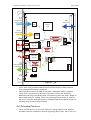
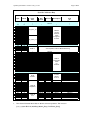
Fig 1 shows the Block Diagram and Layout of OptIF-B.
• OptIF-B processes 12 Command streams:
• Commands and Clocks are accepted from the 50-way front panel connector
• The 12 Command Streams and one of the Clocks are combined using Bi-PhaseMark (BPM) encoding
• The BPM signals are used to drive an array of 12 VCSELs (Lasers) with a
connector interface to a 12-fibre ribbon
• OptIF-B also processes 12 streams of Optical Data:
• accepts Data on a 12-fibre ribbon
• converts to electrical signals
• There is also provision to monitor laser output
• The infra-structure is included to allow control of laser temperature
OptIF-B_Manual.doc of 20/11/02 @ 15:04
Page 2 of 11
4. Detailed Functionality
4.1. Clock and Command
•
•
•
•
Clocks and Commands are accepted from the 50-way front panel connector PL2
as differential LVDS signals. These are 100 Ohm terminated on board.
4 of the available SLOG clocks are used for various on-board clocking functions,
as described below.
The Command Streams pass through the TX- CPLD, which can perform a variety
of operations for lab work: normally the data is passed straight through to the
Opto-TX Plug-In. Four TX-MODE control bits can be set to select the action of
the TX-CPLD.
The Opto-TX Plug-In is the same as that used by the Atlas SCT Back-Of-Crate
card. It uses a BPM12 chip to combine the Clock and Commands using Bi-PhaseMark encoding, and to drive the 12-stream VCSEL array with an MT12 fibre
connector interface to a 12-way fibre ribbon. On board DACs allow the laser
currents to be independently adjusted. Registers in the BPM12 allow control of
the BPM signals.
4.2. Data Streams
•
•
•
•
•
•
•
Optical data is received via an MT12 fibre ribbon connector by the Opto-RX
Plug-In. This is the same as those used by BOC (but see note in the Reference
section)
The Opto-RX has an array of 12 PIN diodes connected to a DRX ASIC. On-board
DACs allow the threshold to be adjusted
The data streams pass through the RX-CPLD: in normal mode this simply passes
the asynchronous data on to the 26-way front panel connector PL1 as LVDS
signals
The operation of the RX-CPLD is selected by 4 RXMode control bits
Pre defined modes are: NORMAL - asynchronous data, 1-to-1 stream mapping,
and PIXEL - data on 6 fibres (2-7 of 0-11) is clocked at 40MHz at two different
phases to provide 12 40MS/s LVDS data streams.
There is provision to pass the data outputs of the RX-CPLD to VME. This gives
the possibility of doing data "Snap-Shots" and capturing short time sequences
(but only with additions to the firmware in the RX-CPLD)
The TX-CPLD can also be re-programmed via the CPLD Programming Header
4.3. The VME Interface
•
•
•
•
•
•
The VME Interface is A24D16 Slave
it responds to Standard Non-Privileged Data Transfers (AM[5:0] = 0x39) and to
Standard Supervisory Data Transfers (AM[5:0] = 0x3D)
the top 8 bits of the VME address (A[23:16]) are tested against the setting of 2
hex switches
all useful registers and functions are accessed through a window of 256 word
addresses, corresponding to A[8:1]
Address bits A[15:9] are not tested
Thus, if the switch settings are ML ("MS" and "LS" switches), the module
occupies the address space from 0xML0000 to 0xMLfffe. But only even
addresses in the range 0xML0000 to 0xML01fe need be used.
OptIF-B_Manual.doc of 20/11/02 @ 15:04
Page 3 of 11
J1
TX
PLD
PL2
Control
PLD
PHOS4
Delays
MSB
Opto TX
Plug-In
Data Streams
To Mustard
LSB
VME Address
TP1
TP2
TP3
TP4
TP5
TP6
TP7
TP8
TP9
TP10
TP11
TP12
TP13
TP14
Patch Board
Sk1
Opto RX
Plug-In
Fuse
ADC
Clocks
from SLOG
VME
Interface
Sk2
Commands
from SLOG
RX
PLD
PL1
CPLD Prog
Header
OptIF_B
•
•
VME transfers are accepted without Bus Error for the entire occupied address
space, even if the particular address has no defined function. Data returned
from unassigned addresses is undefined.
Some operations started by VME access take a substantial time to complete.
These "slow" operations are: Writing to the Laser Current and Threshold
MultiDACs, Writing to the Delay chips, and Converting the Laser Power sample to
digital form ready for reading. There is no pipelining of operations, so conflicts
may occur if further slow operations are attempted. More information is given in
the Reference section of this document.
4.4. Extended Features
•
There is a PIN diode in an ST fibre connector housing together with amplifier
and ADC converter intended for monitoring average laser power. One or more of
OptIF-B_Manual.doc of 20/11/02 @ 15:04
Page 4 of 11
the 12 command streams can be coupled back into this using a suitable fibre
harness.
• It is foreseen that controlling the temperature of the VCSELs may help with
power stability in sensitive applications. Accordingly, the Opt-TX Plug-In can be
equipped with a Peltier heat pump and temperature sensor. There is a site for a
Patch Board with 14 uncommitted connections plus access to the power rails.
• It is also foreseen that this module could be used for the generation of Module
Test Data (both Strip and Pixel), but this will rely on the availability of an OptoTX without BPM encoding
• The TX-CPLD, the RX-CPLD and the Control CPLD can be re-programmed via the
CPLD Programming Header, but this requires detailed understanding of the
hardware, as well as access to the appropriate Lattice CAD and JTAG Download
software.
• The data outputs of the RX-CPLD are accessible from the VME data bus under
the control of the Control CPLD: this gives the possibility of readily adding
features found useful in BOC testing (using the BOC-RIG module):
• Doing a data snap shot
• And, with additions to the RX-CPLD, being able to record a short sequence of
data that can subsequently be read-out over VME
5. Reference Section
5.1. Front Panel Connectors PL1 and PL2
Gnd
D11D10D9D8D7D6D5D4D3D2D1D0-
26
25
20
19
10
9
2
1
Gnd
D11+
D10+
D9+
D8+
D7+
D6+
D5+
D4+
D3+
D2+
D1+
D0+
PL1: MuSTARD Connections
Gnd
D11D10D9D8D7D6D5D4D3D2D1D0NC
NC
NC
NC
NC
NC
NC
NC
CK3CK2CK1CK0-
50
49
40
39
30
29
20
19
10
9
2
1
Gnd
D11+
D10+
D9+
D8+
D7+
D6+
D5+
D4+
D3+
D2+
D1+
D0+
NC
NC
NC
NC
NC
NC
NC
NC
CK3+
CK2+
CK1+
CK0+
PL2: SLOG Connections
OptIF-B_Manual.doc of 20/11/02 @ 15:04
Page 5 of 11
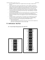
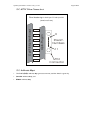
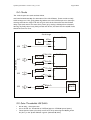
5.2. MT12 Fibre Connectors
Fibre Numbering for both Opto-TX and Opto-RX
Opto-Plug-In
OptIF-B Mother Board
(View from Front)
0
Stream
Numbers
11
Mt12
Connector
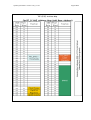
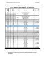
5.3. Address Maps
•
The TOP-LEVEL Address Map gives an overview, and the detail is given by:
•
Detailed Address Map, and
•
BPM12 Address Map
OptIF-B_Manual.doc of 20/11/02 @ 15:04
TOP-LEVEL Address Map
Page 6 of 11
OptIF-B_Manual.doc of 20/11/02 @ 15:04
Page 7 of 11
Detailed Address Map
VME Offset
Byte
Word
1FE
^
198
FF
^
CC
196
CB
194
192
CA
C9
190
18E
C8
C7
18C
18A
C6
C5
188
186
C4
C3
184
182
180
^
C2
C1
C0
^
16E
^
B7
^
102
100
81
80
^
^
096
4B
094
092
4A
49
090
08E
48
47
08C
08A
46
45
088
086
44
43
084
42
082
080
^
41
40
^
020
10
01E
01C
0F
0E
01A
018
0D
0C
016
014
0B
0A
012
010
09
08
00E
00C
07
06
00A
008
05
04
006
03
004
02
002
000
01
00
Function
Hardware
^
^
^
TX_DAC_HI
TX_DAC_LO
Bits
Used
^
Access
^
Unused
^
bit[7:0]
bit[7:0]
bit[7:0]
bit[7:0]
bit[7:0]
bit[7:0]
bit[7:0]
bit[7:0]
bit[7:0]
bit[7:0]
bit[7:0]
bit[7:0]
^
BPM 12
^
Write
Write
Write
Write
Write
Write
Write
Write
Write
Write
Write
Write
Unused
bit[7:0]
bit[7:0]
bit[7:0]
bit[7:0]
bit[7:0]
bit[7:0]
bit[7:0]
bit[7:0]
bit[7:0]
bit[7:0]
bit[7:0]
bit[7:0]
Clock
Phases
bit[4:0]
bit[4:0]
bit[4:0]
bit[4:0]
bit[4:0]
Unused
Write
Write
Write
Write
Write
Write
Write
Write
Write
Write
Write
Write
Unused
Write
Write
Write
Write
Write
bit[7:0]
bit[6,0]
bit[1,0]
bit[3:0]
bit[3:0]
bit[7:0]
bit[7:0]
bit[7:0]
bit[7:0]
Read
R-W
R-W
R-W
R-W
Read
Read
Read
Read
OptIF-B
Info
BPM12
Current
Controls:
0-255
for approx.
0-18mA
^
^
^
Current for Laser 11
Current for Laser 10
Current for Laser 9
Current for Laser 8
Current for Laser 7
Current for Laser 6
Current for Laser 5
Current for Laser 4
Current for Laser 3
Current for Laser 2
Current for Laser 1
Current for Laser 0
^
See Separate Table for BPM Addressing
^
RX_DAC_Odd
RX_DAC_Even
RX_DAC_Odd
RX_DAC_Even
RX_DAC_Odd
RX_DAC_Even
RX_DAC_Odd
RX_DAC_Even
RX_DAC_Odd
RX_DAC_Even
RX_DAC_Odd
RX_DAC_Even
^
OptIF-B
Registers
Acts
On
Description
^
Threshold for Stream 11
Threshold for Stream 10
Threshold for Stream 9
Threshold for Stream 8
DRX12
Threshold for Stream 7
Thresholds:
Threshold for Stream 6
0-255
Threshold for Stream 5
for
Threshold for Stream 4
0-255uA
Threshold for Stream 3
Threshold for Stream 2
Threshold for Stream 1
Threshold for Stream 0
^
BPM Clock
PHOS4
TX_Clock1
Delays:
TX_Clock0
0-24 ns
RX_Clock1
RX_Clock0
Reserved
Spare
Reserved
Spare
Reserved
Spare
Laser Power Monitor
Monitor ADC
Control Word Control/Status in a Word
Resets
MDAC_Reset,BPM_Reset
Command Stream Mode
TX_Mode
Data Stream Mode
RX_Mode
CB (Hex)
Manuf
45 (Dec)
Module Type
00-FF
Module Vers
00-FF
Firmware Vers
Notes:
1.
The Control/Status Word has no Write action at present. The bits are:
[x,x,x,x,LaserBlockIn,ADCBusy,MDAC_Busy,ClockPhase_Busy]
OptIF-B_Manual.doc of 20/11/02 @ 15:04
Page 8 of 11
BPM12 Address Map
Notes:
1.
To ensure the BPM internal test circuits are inactive, write 0x20 to MLx160 and
0x40 to MLx168
2. BPM registers are Read/Write: unused bits are undefined when Read, Don't-Care
when Written
OptIF-B_Manual.doc of 20/11/02 @ 15:04
Page 9 of 11
5.4. Clocks
The 4 Clock inputs are used as shown below.
See Detailed Address Map for addresses of the Clock Phases. These are Write-Only.
Valid settings are 0-24, giving phase adjustment over the full 25ns period in 1ns steps.
Settings outside the range 0-24 will not give valid clocks. Note also that the PHOS4
delay chips used need to be reset after power up by issuing a dummy Write command.
Writing any delay value to any delay stream will do this, but note that the SLOG clocks
should be turned on first.
Clock Usage
Xtal
Osc
Control CPLD
SCk0
SC0
CK_Ph0
SLOG Clocks
XOsc
SC1
CK_Ph1
CK_Ph2
SC2
CK_Ph3
RX-Ck0
RX CPLD
RX-Ck1
TX-Ck0
TX CPLD
TX-Ck1
TX Plug-In
SC3
CK_Ph4
BPM-Ck
BPM12
5.5. Data Thresholds: RX-DACs
•
•
•
Write-Only - Slow Operation
Set to 0-255 for Thresholds of 0-255uA (approx. 0-500uW optical power)
These (and the Laser Currents) are all set to 0 by asserting the MDAC_Reset
bit (bit 1) in the OptIF-B Reset register (address MLx00c)
OptIF-B_Manual.doc of 20/11/02 @ 15:04
5.6. Laser Currents: TX-DACs
•
•
•
Page 10 of 11
Write-Only - Slow Operation
Set to 0-255. This is a non linear control: there is around 1mA of laser current
up to a setting of around 95. Thereafter the current increases roughly linearly
to around 18mA for a setting of 255. Lasing will not start until the threshold
current is reached (around 3mA). The maximum power output per laser (with the
currently available Opto-TX Plug-Ins) is 2200uW (1200uW average over any
50ns period).
These (and the Data Thresholds) are all set to 0 by asserting the MDAC_Reset
bit (bit 1) in the OptIF-B Reset register (address MLx00c)
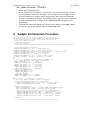
6. Sample Initialisation Procedure
// ********************************************************
short init_IFB(short p) // This routine may contain some debris
// ********************************************************
{ short dd,ee,ff,stream,dacv ;
unsigned short errors;
// Laser DAC settings
short int lasi[12]= {0xc0,0xc0,0xc0,0xc0,0xc0,0xc0,0xc0,0xc0,0xc0,0xc0,0xc0,0xc0} ;
printf("OptIF-B Module Info:\n");
VXIpeek(IFB_CREGS+0x2,2,&ee); // Read Module Type
VXIpeek(IFB_CREGS+0x1,2,&ff); // Read Module Version
printf("..Module Type and Version is: %03iv%02X\n", ee & 0xFF, ff & 0xFF) ;
VXIpeek(IFB_CREGS+0x3,2,&ee); // Read Module Manuf
printf("..Manufacturer is: %02X\n", ee & 0xFF) ;
VXIpeek(IFB_CREGS+0x0,2,&ee); // Read Firmware version
printf("..Firmware version is: %03i\n\n", ee & 0xFF) ;
//
// first set up PHOS4s to ensure there's a 40MHz clock
//
... Note SLOG will need clocks enabling first
VXIpoke(IFB_CLOX+0,2,0) ; // Dummy
VXIpoke(IFB_CLOX+0,2,0) ; // RX_Clock0
VXIpoke(IFB_CLOX+1,2,0) ; // RX_Clock1
VXIpoke(IFB_CLOX+2,2,0) ; // TX_Clock0
VXIpoke(IFB_CLOX+3,2,0) ; // TX_Clock1
VXIpoke(IFB_CLOX+4,2,0) ; // BPM_Clock
// Now reset BPM and DACs:
VXIpoke(IFB_CREGS+6,2,3);
VXIpoke(IFB_CREGS+6,2,0);
// now rest of CREGS
VXIpoke(IFB_CREGS+4,2,0); // RXMode
VXIpoke(IFB_CREGS+5,2,0); // TXMode
//
dacv = 0x80 ; // Ball park ... 16-Nov-02
// now set up TXDACS and BPM registers to defaults
for(stream=0;stream<12;stream++) // set up DACs
{ VXIpoke(IFB_TXDAX+stream,2,lasi[stream]); // laser currents
VXIpoke(IFB_RXDAX+stream,2,dacv);
// Thresholds
}
// Common BPM Registers
VXIpoke(IFB_BPM+0x30,2,0x20); // Inhibit RAND and TRIGGER Outputs
VXIpoke(IFB_BPM+0x34,2,0x40); // Inhibit Internal Clock
for(stream=0;stream<12;stream++) // per stream BPM registers
{ VXIpoke(IFB_BPM+0+4*stream,2,0x00); // Stream Inhibit=0 (0 or 1)
VXIpoke(IFB_BPM+1+4*stream,2,0x12); // Mark-Space
(0-0x1f)
VXIpoke(IFB_BPM+2+4*stream,2,0x00); // Coarse delay (0-0x1f)
VXIpoke(IFB_BPM+3+4*stream,2,0x00); // Fine delay
(0-0x7f)
}
return(0);
} // ********************************************************
OptIF-B_Manual.doc of 20/11/02 @ 15:04
Page 11 of 11
7. Additional Info
•
•
Opto-Plug-Ins … connectors: the Opto Plug-Ins available to date use an array of
individual pins as the connector to the motherboard (34 for the Opto-RX, 38 for
the Opt-TX). Future Plug-Ins will use a 40-pin Samtec connector with 0.8mm
spacing. An adapter card will be available to allow the new Plug-Ins to be used on
OptIF-B.
Slow Operations:
• Laser Current settings .. take about 20us to complete
• Data Threshold settings.. take about 20us to complete
• Clock Phase settings .. take about 200us to complete
The general idea is that starting such operations will not result in the VME
transfer being held up. But any subsequent VME Write to OptIF-B will be held
up until the slow operation is complete (the VME Acknowledge is withheld). Such
a "hang-up" can be avoided by Reading the OptIF-B Status word - Reads are not
held up by any slow operations - and looking at the MDAC_Busy and
ClockPhase_Busy bits (bits 1 and 0). The following IFB_WPOKE() function does
this testing before writing:
// ********************************************************
void IFB_WPOKE(unsigned short *addptr, UINT16 a)
// ********************************************************
{
UINT16 count,busy;
busy = 1;
for(count = 0;((count<1000) && busy);count++)
{ VXIpeek(IFB_CREGS+7,2,&busy);
busy = busy & 0x3;}
if (count < 1000)
{ VXIpoke(addptr,2,a);
return;}
else
{ printf("IFB_WPOKE: timeout\a\n");
return;}
}
// ********************************************************
•
•
Reading the Laser Power Monitor (not yet fully implemented) is also a slow
operation involving starting a conversion that takes about 1.5us to produce an
answer for reading. The plan is that the first read yields rubbish data, but kicks
off a sample and conversion. Bit 2 of the Status word (ADCBusy) goes high until
the conversion is complete. The next Read of the Power Monitor gives the
reading, and kicks off another conversion.
Sample Initialisation Procedure for OptIF-B
…oo0oo…