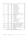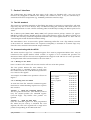
1
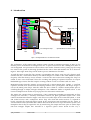
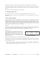
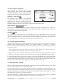
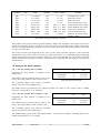
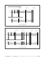
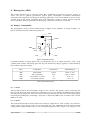
APV6 User Manual
Author:
Email:
M.French
[email protected]
Phone:
Fax:
+44 1235 446484
+44 1235 445753
Post:
Rutherford Appleton Laboratory
Chilton
Didcot
Oxon
OX11 0QX
United Kingdom
Version:
1.0
Notes:
This is a working document that will be updated frequently. Please pass
comments and requests for the inclusion of more information to the above
author.
apv6_manual.doc
Version: Draft
1
16/10/96
1 . Document History
Date
Revision
Number
Description
16/10/96
1.0
First draft version
apv6_manual.doc
Version: Draft
2
16/10/96
2 . Contents
1.
Document History
2.
Contents
3.
Related Documents
4.
Introduction to the APV6 and Analogue Read-out in the CMS Tracker
5.
Physical Size and Pad Layout
6.
Logic Levels
7.
Control Interface
8.
Biasing the APV6
9.
Running the APV6
10. Data Output Format
11. Using the Internal Test Pulse System
12. Other Features
apv6_manual.doc
Version: Draft
3
16/10/96
3 . Related Documents
Name
Author
Notes
Specifications for the
Control and Read0out
Electronics for the CMS
Inner Tracker
A. Marchioro
CMS Working document
APV6 Requirements
M.French
Part of the RAL QA project specification
Balaton Paper
M.French
Presented at 2nd LHC workshop on electronics
apv6_manual.doc
Version: Draft
4
16/10/96
4 . Introduction
Copper differential low voltage drive
APV6
APV6
APV6
APV6
APV6
APV6
APV6
APV6
APV6
APV6
APV6
APV6
Link driver chip
Quad laser unit
Mux driver
-A
-A
-A
-A
APV6
APV6
APV6
APV6
-A
-A
-A
-A
APV6
APV6
PLL timing trim chip
I2C
Link
Optical ribbons to FED module
LVDS
CK and T1
Figure 1: Analogue Read-out in the CMS silicon tracker
The architecture of the CMS tracker readout system is based on analogue processing of data in t h e
detector prior to transmission in analogue form via an optical interface to the counting room. Here i t
will be digitised and processed to remove offsets and reorder channels before passing up the DAQ
tree. Some of the system is still being specified but the silicon front end modules will be as shown in
Figure 1. Here eight APV6 chips will be used to process 1024 detector channels.
As with the APV5 version the chip contains a preamplifier and shaper stage for each channel. Each
channel then has a 160 location memory into which samples are written at the LHC 40MHz machine
frequency. Thus the memory always contains a record of the most recent beam crossings the chip has
sensed. A data access mechanism allows the marking and queuing of requested locations for output.
Embedded logic ensures that the samples awaiting readout are not overwritten with new data.
Requested samples from the memory are processed with a deconvolution filter (APSP), a switched
capacitor network, that deconvolves the shaping function of the preamplifier and shaper stages to
recover the initial pulse shape. After the APSP the data is held in a further memory buffer prior to
switching through an output analogue multiplexer. This additional buffer is required so that as one
event is multiplexed out another may be prepared for consecutive transmission.
The APV6 also contains features required for a final CMS design including programmable on chip
analogue bias networks, a remotely controllable internal test pulse generation system and a slow
control communication interface. Figure 1 also shows two other chips on the Front-end hybrid, a clock
and control receiver and a multiplexer driver chip. The clock and control receiver is required to
locally generate the clock and trigger signals in the appropriate form and timing for the APV6. I t
will also interface the hybrid I2C slow control data bus to the next level up in the control system. The
multiplexer driver chip is required to mix, by interleaving, the output data from pairs of APV6 chips
onto four analogue outputs that transmit to a separate optical driver board. In this way a
apv6_manual.doc
Version: Draft
5
16/10/96
multiplexing level of 256 to 1 is achieved at the hybrid output. Both of these chips are in design a t
RAL and CERN for fabrication in radiation soft form.
apv6_manual.doc
Version: Draft
6
16/10/96
5 . Physical Size and Pad Layout
The overall dimensions of the APV6 chip are shown in Figure 2 below.
Four groups of
32 input pads
1
INP<127>
VSS
APV6
GND
VDD
1
13
INP<0>
37
Bias monitor pads
Back-end pads
Figure 2: APV6 overall dimensions (dimensions in microns)
The design will be fabricated using the standard Harris AVLSI-RA process flow. The wafers will be
of 4 inch type and 19mils (approx. 500um) thick. A table showing the precise co-ordinates of t h e
centre of each pad may be obtained from RAL, please request it if required.
5.1 Analogue inputs
The 128 analogue inputs are grouped into four sections of 32. Each section is separated by larger power
supply pads. These power connections supply the preamplifier stages (where most of the APV6 power
is used) and must be bonded to supplies close to the chip. Use the shortest bond length and multiple
bonds if possible (to minimise inductance).
Note: The reason for powering the chip in this way is so that the power losses in the APV6
routing, and the area wasted in large power buses is minimised.
Each group of inputs is arranged in two staggered rows, each rows pads are spaced at 86um. The inner
row is offset 43um clockwise (viewed from the centre of the APV6). Thus the effective bond pitch
within each group is 43 um. Each pad is 100um long and 60um wide (the passivation opening is about
3um smaller than this). The pads are labelled from <0> to <127>. The Inp<0> is on the lower left of
the first group and Inp<127> is at the top right of the top section.
The analogue inputs all have small protection diodes to VSS and VDD. These are not intended to
meet standard levels of protection but should prevent damage during assembly if reasonable antistatic measures are taken. For them to work effectively the VDD GND and VSS pads should be
bonded first and grounded to the assembly machine.
5.2 Bias monitor pads
These are intended for test purposes only. They enable a direct measurement of the bias voltages and
currents set in the bias generator. The first test systems should permit bonding to these points to allow
apv6_manual.doc
Version: Draft
7
16/10/96
the user to monitor or override the levels generated internally. There are thirteen test points and
they are tabulated below:
Pad Number
Name
Type
Measure to
1
V_BG
current
VSS
2
IPRE
current
VSS
3
VPRE
voltage
GND
4
VCAS(P)
voltage
GND
5
ISFB(P)
current
VSS
6
ISHA
current
VSS
7
VSHA
voltage
GND
8
VCAS(S)
voltage
GND
9
ISFB(S)
current
VSS
10
IPSP
current
VSS
11
VADJ
voltage
GND
12
CLVL
current
VSS
13
VDEL
voltage
GND
Table 1: Bias monitor points
Note that when measuring a current
by connecting the meter to VSS t h e
current flows in the meter and is
starved from the internal mirroring
in the APV6. This means that t h e
measurement will prevent the chip
from working, during operation these
points must normally be left open
circuit.
The VCAS and ISFB have two
entries even though each has only
one control word in the bias
generator. This is because they are
required both in the preamplifier
and the shaper. To prevent possible
undesired feedback the reference for
the two stages are independently
mirrored out of the bias generator
and consequently appear at two
pads.
The pads V_BG and VDEL both do not relate directly to bias channels. V_BG can be used to measure
the reference current for the bias generator, this prevents the bias generator mirrors from working so
must not be made at the same time as any other measurement, the nominal value for this current is
128uA. VDEL is connected to the calibration delay line. When the calibration feature is enabled
(calibration inhibit OFF) this voltage should “hunt” (small steps up and down in voltage around t h e
optimum bias point for the delay elements). Monitoring this voltage and observing the “hunt” effect
will indicate that the delay line has successfully locked onto the clock. See section “APV6 Using t h e
internal calibration system” for more details. External capacitance connected to the VDEL pad will
slow down the “hunt” effect and so may upset the measurement.
5.3 Backend Pads
All of the IO, address pads and remaining power supply pads are located down the back edge of t h e
chip. There are 37 in total and a full list describing their function is shown in Table 2. The pads are
approx. 100um by 60um and are on a 150um pitch. There is one pad “gap” next to the current output and
the fast differential input pairs (clock and control) have an additional 50um spacing from their
neighbours.
Normally all of the pads of type “TEST” may be left unconnected. They are designed for use in test
and early evaluation of the chip. The pads of type “BIAS” may be left unconnected (with t h e
exception of BRES which should be connected to the -2V supply) if the internal bias reference is used.
For details of how to use an external reference or the reference propagation system see section XXX.
The clock and trigger inputs are of low voltage differential type, the remaining inputs require
switching between +2 and -2V. The pads PORT, SCLK and SDIN have a hysteresis characteristic
because the expected edges on these signals may be very slow.
apv6_manual.doc
Version: Draft
8
16/10/96
Pad Position
Name
Type
Function
1
AVSS
POWER
Analogue -2V Supply
2
AVDD
POWER
Analogue +2V Supply
3
CAL0
TEST
Charge injection test point
4
CAL1
TEST
Charge injection test point
5
CAL2
TEST
Charge injection test point
6
CAL3
TEST
Charge injection test point
7
BINP
BIAS
Bias reference override input
8
BRES
BIAS
Internal bias reference -2V supply
9
BOT1
BIAS
Reference current output
10
BOT2
BIAS
Reference current output
11
BOT3
BIAS
Reference current output
12
BOT4
BIAS
Reference current output
13
BOT5
BIAS
Reference current output
14
BOT6
BIAS
Reference current output
15
PROBE
TEST
Pad connected to -2V supply for probe edge sensor
16
AOUT
OUTPUT
17
PORT
INPUT
Power On Reset Pad
18
ADD0
INPUT
APV Address bit
19
ADD1
INPUT
APV Address bit
20
ADD2
INPUT
APV Address bit
21
ADD3
INPUT
APV Address bit
Current mode analogue output
200um GAP
22
OUTE
OUTPUT
Digital output, switches low when analogue data is output
23
SDOT
OUTPUT
I2C Data Output
24
WPTK
TEST
Memory write pointer test point
25
TPTK
TEST
Memory trigger pointer test point
26
DEL1
TEST
Calibration unit test point 1
27
DEL2
TEST
Calibration unit test point 2
28
DVDD
POWER
29
AGND
GROUND
30
HERA
INPUT
Digital +2V pad
Analogue Ground Connection
Tie to +2V for HERA mode or -2V for normal (LHC) mode
100um Gap
31
CLKN
INPUT
40MHz clock negative input (low voltage type)
32
CLKP
INPUT
40Mhz clock positive input (low voltage type)
33
TRGN
INPUT
34
TRGP
INPUT
100um Gap
Trigger negative input (low voltage type)
Trigger positive input (low voltage type)
100um Gap
35
SDIN
INPUT
I2C data input
36
SCLK
INPUT
I2C clock input
37
DVSS
SUPPLY
Digital -2V supply
Table 2: Backend pad listing, Pads (100um by 50um) spaced at 50um unless specified otherwise
apv6_manual.doc
Version: Draft
9
16/10/96
6 . Logic Levels
6.1 Digital
6. 1. 1 INPUT
6 . 1 . 2 INPUT (Low Voltage Type)
6 . 1 . 3 OUTPUT
6.2 Analogue
6 . 2 . 1 TEST inputs
6 . 2 . 2 OUTPUT
apv6_manual.doc
Version: Draft
10
16/10/96
7 . Control Interface
The configuration, bias setting and error states of the APV6 are handled with a two wire serial
interface. It is designed to conform to the Phillips I2C standard so that it may be controlled by a
standard off the shelf components (e.g. PCD8584 parallel bus interface chip).
7.1 The I2C standard
This protocol is specified completely in the Philips data books so need not be repeated here. The APV
chips may only act as slave devices. They are addressed using the standard 7-bit mode where t h e
most significant bits are “001” and the remaining 4 bits are defined by bonding out address pads on t h e
APV6.
The 4 address pads (ADD0, ADD1, ADD2, ADD3) each possess internal pull-up resistors (of approx.
80Kohm) to VDD. Selective bonding of these pads to VSS therefore allows any address pattern to be
set. The APV will only execute the requested command if the 3 most significant bits are “001” and t h e
4 remaining bits match the bonded address setting.
The APV address “1111” is reserved for “global” addressing. When the “1111” chip address is used in
an i2c transfer all connected APVs will respond. Consequently a maximum of 15 APV6 chips may
share the same controller and maintain unique addresses.
7.2 Communicating with the APV6
The APV6 interface logic has a command register that must be programmed before data may be
transferred. This register defines which variable or register is to be accessed and specifies t h e
direction of data transfer. The least most significant bit is high for read and low for write operations.
A complete table of the command codes is shown in Table 3.
7 . 2 . 1 Writing to the APV6
Data is written to the APV6 with one I2C transfer with two 8 bit data packets.
The first packet defines the APV address, t h e
second specifies a command register (in both cases
the read bit must be low) and the third specifies the
new value for the register.
Function or Variable
Command
Register Code
An example of an IPRE write operation is shown in
Figure 3
Error register
Mode register
00 00 00 1X
7 . 2 . 2 Reading from the APV6
Latency register
00 00 01 0X
To read data from the APV6 the command register
must first be written. Reading requires two separate
I2C transfers.
00 00 00 01
IPRE
01 00 00 0X
ISHA
01 00 00 1X
IPSP
01 00 01 0X
ISFB
01 00 01 1X
VPRE
01 00 10 0X
The first packet defines the APV address (read bit
low), the second specifies the command register
(read bit high). Any further data packets are
ignored.
VSHA
01 00 10 1X
VADJ
01 00 11 0X
VCAS
01 00 11 1X
CLVL
01 01 00 0X
Transfer 2
Read the data back
CSKW
01 01 00 1X
Once the command register has been programmed
the APV6 may be read by a standard I2C read
sequence, the APV will respond with a single 8-bit
packet corresponding to the addressed data.
CDRV
01 01 01 0X
Transfer 1
apv6_manual.doc
Write the command register
Version: Draft
11
Table 3: Command Register Codes
16/10/96
Subsequent reads of the same register is possible without re-programming the command register.
If the APV is addressed as “global” for reading all APVs will respond. The serial data output is of
open drain type so if more than one APV6 responds the logical AND of all addressed APV’s will be
sensed.
An example of an IPRE read operation is shown in Figure 4.
7.3 Command register codes
The command register codes are 8-bit with the last bit determining the direction of transfer.
The command codes are listed in Table 3 with MSB first, X=1 for read operations, X=0 for write
operations.
7.4 Error register definition
For short periods the APV6 may be triggered at a rate faster than it can output data. When this
happens a queue develops in the APV6. The length of this queue is limited by the number of spare
locations in the memory and an address fifo that stores the addresses of columns awaiting read-out.
As the queue grows, depending on the latency programmed, eventually the fifo becomes full or all t h e
available memory locations become allocated. Either case leads to pipeline failure. The circuit must
then be reset with a RESET101 sequence to clear the fault.
Fifo error
The fifo error is simply found by keeping a record of the number of addresses stored (limit=19). In
deconvolution mode three addresses must be stored for each trigger, so in this case the limit is six
triggers. For peak processing where only one address is stored the limit is nineteen.
Latency error
The memory function is continuously monitored by a
latency test (the separation between the write and
trigger pointers should always be equal to t h e
programmed latency). This is checked every time
the memory is overwritten (at least once every 160
pipeline clock cycles).
Error
Value = 0
Value = 1
<1>
fifo error
OK
<0>
latency error
OK
Table 4: Error register definition
The function of the error register is to report these two classes of failure.
The error bits are active low so that its possible to read a group of APVs in one go with the “global”
read operation, the “wire-and” of the open drain outputs pulls the output low if any of the APVs
have the appropriate error.
Note: When a new latency value is written a Latency Error will inevitably be produced. T h e
pipeline must be restarted to initialise the pointers with the new separation. This must be done
with a RESET101 sequence which will also clear the Error.
apv6_manual.doc
Version: Draft
12
16/10/96
7.5 Mode register definition
Three functions are controlled by the APVs
“Mode” register. They default to the underlined
conditions tabled below (at power-up) and may be
read and overwritten (not altered by RESET101).
Calibration inhibit OFF/O N
Mode
Value = 0
Value = 1
<2>
calibration
inhibit OFF
calibration
inhibit ON
<1>
“deconvolution”
“peak”
processing
processing
<0>
analogue bias
analogue bias
The calibration logic contains a self regulating
OFF
ON
“clocked” delay line may cause noise in t h e
system. For this reason it should be inhibitted
Table 5: Mode register definition
when not in use. At power on it defaults to t h e
inhibitted condition. The use of this function is fully described in section XXX.
APSP operation Deconvolution/ P e a k
Deconvolution mode enables the three sample weighted deconvolution algorithm that confines t h e
shaped signal to one beam crossing (suited to LHC operation). When operating in “Peak” mode only
one sample is stored and is output directly.
Analogue O F F/ O N
The analogue bias control allows the bias conditions of the chip to be disabled whilst the required
values are programmed into the bias generator. Enabling analogue bias then lets the programmed
values to take effect. This is particularly useful at power-up where the default is “OFF”, thus t h e
power consumption of the system may be ramped up in a controlled fashion.
7.6 Latency register definition
This register contains a binary number that defines the separation between the “Write” and “Trigger”
pointers in the analogue memory controller. The register defaults at power-up to a value of
bit<7:0>=10000100. This corresponds to a count of 132 clock cycles. This value may be reprogrammed to
any value up to 156.
Note: Programming larger values of latency reduces the cells available for queuing output d a t a ,
and will impact on the efficiency of the APV6 at high trigger rates.
To program a new latency the binary number equivalent to the required number of pipeline cycles must
be written by an I2C write operation. Then the circuit must be reset with a RESET101 trigger sequence.
In “Peak” mode this number represents the number of exact clock periods between a signal being sensed
at an analogue input and outputting the sample on the peak of the CR-RC shape. In deconvolution
mode the first sample must be three clock cycles before that point. Thus in deconvolution mode to get
the same effective latency the number programmed must be three counts larger.
7.7 Bias generator settings
The bias of the analogue stages in the APV6 is controlled by an internal “Bias Generator” part. There
are three classes of bias; current, voltage and charge.
The bias block produces only current in each case. Currents are output directly, voltage bias levels are
then generated by internal termination resistors chosen to give appropriate ranges of adjustment, and
charges are generated by switching the current into load resistors and then converting the voltage
step generated to charge with a series capacitance.
The bias part requires a reference current from which all of its levels are scaled. This is generated
internally with a resistor network but may be overridden by an external source.
apv6_manual.doc
Version: Draft
13
16/10/96
Bias Name
Class
Range
Resolution
Value (n = 0 to 255)
Description
IPRE
I
0 to 1020uA
4uA
n 5 4uA
Preamplifier bias current
ISHA
I
0 to 255uA
1uA
n 5 1uA
Shaper bias current
IPSP
I
0 to 127.5uA
0.5uA
n 5 0.5uA
ISFB
I
0 to 255uA
1uA
n 5 1uA
APSP bias current
Source follower bias current
VPRE
V
VDD to VSS
18mV
VDD - (n 5 18mV)
Preamp feedback bias voltage
VSHA
V
VDD to VSS
18mV
VDD - (n 5 18mV)
Shaper feedback bias voltage
VADJ
V
GND to VSS
9mV
GND - (n 5 9mV)
Output level adjustment
VCAS
V
GND to -1.02V
4mV
GND - (n 5 4mV)
Cascode voltage bias level
CLVL
Q
0 to 15.3fC
0.06fC
n 5 0.06fC
Reference for internal charge
injection system
Table 6: Bias control range and resolution (128uA bias)
The nominal value for the reference current should be 128uA. The resolution and ranges for each bias
setting are derived from that reference, so will scale if this is overridden. The voltage and charge
accuracy also depend on the polysilicon resistance used in the internal conversion resistance. This may
vary by as much as 20%.
The charge accuracy also depends on the value of the series injection capacitor. These injection
capacitors are close to the scribe of the chip, for yield reasons they are constructed using overlapping
metal1 and metal2. This gives a further variation in the charge injected. For the above reasons t h e
charge injection scale must be measured or calculated at test, recorded and then used to scale absolute
measurements.
7.8 Example I2C Write transfers
7 . 8 . 1 Set the preamp bias to 500uA
Hex
Supposing the chip address is bonded to t h e
pattern 0101.
The address byte is 00101010 2A(hex). This is 001
(APV), 0101 (chip address) and 0 for I2C write.
Binary
Address Byte
2A
00101010
Command Byte
40
01000000
Data Byte
7D
01111101
Table 7 Example preamp bias write
The command register byte must be 01000000
40(hex) see Table 3 (write IPRE entry).
The IPRE current is governed by the equation n54uA (see Table 6), the closest value of 488uA
therefore corresponds to a “n” of 7D(hex).
7 . 8 . 2 Set the preamp bias voltage to 0.5V
Supposing the chip address is bonded to t h e
pattern 0101.
The address byte is 00101010 2A(hex). This is 001
(APV), 0101 (chip address) and 0 for I2C write.
Hex
Binary
Address Byte
2A
00101010
Command Byte
48
01001000
Data Byte
53
01010011
Table 8 Example preamp bias voltage write
The command register byte must be 01001000
48(hex) see Table 3 (write VPRE entry).
The VPRE voltage is governed by the equation VDD – (n 5 18mV) see Table 6, assuming VDD of 2V,
0.506V corresponds to a “n” of 53(hex).
apv6_manual.doc
Version: Draft
14
16/10/96
Structure of an APV I2C Write command sequence:
CHIP ADDR
001=APV
3
SDA
SCK
2
1
ACK (From APV)
SCK(From APV)
R/W
ACK (From APV)
0
7
APV Write Call
6
5
4
3
2
1
0
7
6
5
APV Control register
4
3
2
1
0
New APV data
Example: Write Preamp bias of 488uA to APV chip "0101"
SDA
SCK
APV Write Call
APV Control register
New APV data
Figure 3: Example I2C write
Structure of an APV I2C Read command sequence:
3
SDA
SCK
2
1
0
APV Write Call
CHIP ADDR
001=APV
7
6
5
4
3
2
1
0
3
APV Control register
SCK(From Controller)
SCK(From APV)
2
1
0
R/W
CHIP ADDR
001=APV
ACK (From APV)
R/W
ACK (From APV)
7
6
5
4
3
2
1
APV Read Call
Data From APV
APV Read Call
Data From APV
0
Example: Read Preamp bias (Value set to 122 decimal i.e. 488uA)
SDA
SCK
APV Write Call
APV Control register
Figure 4: Example I2C read
apv6_manual.doc
Version: Draft
15
16/10/96
7 . 8 . 3 Set mode register
Hex
Supposing the chip address is bonded to t h e
pattern 0101, and we want to set calibration logic
to off, enable “peak” processing and enable t h e
analohue bias to all APV chips.
Binary
Address Byte
3E
00111110
Command Byte
02
00000010
Data Byte
07
00000111
Table 9 Example mode register write
The address byte is 00111110 1E(hex). This is 001
(APV), 1111 (global address) and 0 for I2C write.
The command register byte must be 00000010 02(hex) see Table 3 (write Mode register).
The three bits used in the register must all be set to “1” see Table 5. Programme 00000111 i.e. 07(hex),
the leading zeros are ignored.
7.9 Timing
The I2C standard is specified at 400 kbit/s. This is so that bus capacitances of 200 to 400pF may be
used with reasonable values of pull-up resistance. The APVs internal logic is capable of running a t
speeds much higher than this, even up to 40Mhz. The limiting factor is the external load capacitance
and resistance.
The SCK and SDA inputs both have a hysteresis chractersitic of 0.5V(min) and will switch within
the range of +/-1V.
The output resistance of the SDA output pad is approximately 500 ohms (when pulling low). To ensure
that this is capable of pulling the SDA line below -1V, pull up resistors of 2K2 or higher must be used.
If the pull-up is of current source type this should be no greater than 1.5mA.
7.10 Pad Specification
Since the APV may only ever act as a slave device, it need never drive the clock line. For this reason
the clock SCK connects to one input pad “SCLK”. The data line is bidirectional, for easy test this has
been split into two pads that may be shorted external to the chip. The data input pad to the APV is
called “SDIN”. The data output pad is called “SDOT”.
The Full list of pads and their description may be found in the section “Physical Layout of t h e
APV6”.
apv6_manual.doc
Version: Draft
16
16/10/96
8 . Biasing the APV6
This section describes how to bias the APV6. Bias adjustment is necessary for several reasons. I t
allows the user to optimise performance against power consumption, accomodate manufacture
tollerences and compensate for changes in operating point that arise from irradiation of the circuit.
At each stage in the signal processing chain each adjustable variable is listed and the expected
effects described. Finally a procedure for biasing up a chip for the first time is outlined.
8.1 Stage 1: Preamplifier
The preamplifier circuit is shown schematically in Figure 5. The amplifier is charge sensitive, its
gain is determined by the feedback capacitor Cf.
VPRE
Rf
IPRE/10
Cf
Input
Output
VCAS
IPRE
ISFB
Figure 5: Preamplifier schematic
It should respond to a charge signal with a proportionate step at its output and decay with a long
(>500ns) time constant. The charge gain (the step size divided by charge applied), is determined by
the feedback capacitor, 0.25pF.
Name
Principle Effect
Nominal Value
Reasonable Range
IPRE
Preamp Noise
500uA
200uA to 1mA
20uA to 100uA
ISFB
Output impedance
50uA
VCAS
Accomodates Vt change
0V
0V to -1V
VPRE
Vary Preamp fall time
-0.4V
+1V to -1V
Table 10: Preamp Bias Summary
8. 1. 1 I P R E
This sets the current in the preamplifier stages of each channel. The primary effect of altering this
bias is on the electronic noise and power consumption. At very low settings an additional effect will be
that the preamps output rise time will increase, this then increases the rise time of the shaped signal
increasing the peaking time. Assuming a chip bias of 128µA the IPRE value set follows the relation
IPRE=(n 5 4µA).
8. 1. 2 ISFB
This controls the amount of current in the source follower output device. This variable also controls a
similar stage in the shaper stage. It is not expected that any adjustment from the 50uA nominal
setting will be required. If this is set too low the output impedance of the shaper will drop, this will
apv6_manual.doc
Version: Draft
17
16/10/96
lead to loss of signal height and distortion of the pulse shape. Assuming a chip bias of 128uA t h e
ISFB value set follows the relation ISFB=(n 5 1µA).
8. 1. 3 VCAS
The preamplifiers output source follower is Ntype, the operating point of the output node is
determined by the pmos input device. Nominally the output voltage is expected to be around -1.2v, I t
is important the cascode device stays in saturation, this means that its drain must be above its gate
voltage. To ensure that the cascode device can be maintained in saturation, adjustment of VCAS may
be required. The effect of a to high VCAS bias will be a drop in open-loop gain, this will cause poor
pulse shape and noise performance. Before irradiation the expected optimal setting for this bias is 0v
dropping to -0.5v after irradiation. The VCAS value set follows the relation VCAS=GND – (n 5
4mV).
8. 1. 4 VPRE
The function of the preamp is to provide a voltage step to the shaper, to prevent pile-up effects a long
tail is required. The effect of adjusting VPRE on the preamp and shaper output is shown in figure X
below.
Figure 6: The effect of changing VPRE
The higher voltage set the smaller the feedback resistance (and therefore the time constant)
becomes. Assuming a chip bias of 128uA the VPRE value set follows the relation VPRE= VDD – (n 5
18mV).
8.2 Stage 2: Shaper
The shaper amplifier circuit uses the same architecture as the preamplifier.
apv6_manual.doc
Version: Draft
18
16/10/96
9 . Running the APV6
Once set-up the APV6 requires only one control line, TRG, to run. This control line is normally held a t
zero. It is possible to send three commands on it, a TRIGGER (a single “1”), a CALIBRATE REQUEST
(a double “11”) and a RESET101 (two “1” separated by a gap). Consequently consecutive triggers or
triggers next to calibration requests may get confused with the reset signal, for this reason the user
must inhibit these occurances. RESET101 signal is used to clear the pipeline and initialise t h e
memories pointer system. After power-up and appropriate programming of the various control
registers described in the previous section a RESET101 is required after which the TRIGGER or
calibration requests can be sent.
The trigger latency is the time (in the number of pipeline clock cycles) between a detector signal being
applied to an APV6 input and the cycle that the TRIGGER signal must be applied to the chip to
output that signal at its peak. This number corresponds to the separation of pointers in the memeory
that specify the read and write locations.
9.1 Sending a RESET101
A RESET101 sequence clears any pipeline pointers and relaunches them with the programmed latency
separation. The 101 sequence, is really sensed by the chip as 1X1, so the sequence 111 will have t h e
same effect. In fact any train of consecutive “1”s of at least 3 will cause a RESET101. In the case of
extended reset sequences the reset is not released until the end of the sequence.
Pipeline Pointer
Separation
Trigger signal
6
int(Write Pointer)
int(Read Pointer)
Initialisation Phase
Triggers valid from
this point
Figure 7: Reset and initialisation process
An example in shown in Figure 7, here a RESET101 is applied and internal signals are then generated
to start the write and trigger pointers. The separation of these signals corresponds to the value
programmed in the “Latency” register. No triggers should be sent whilst this initialisation process is
in progress as errors may result. For this reason no triggers should be sent within 6 clock cycles of
prgrammed latency.
9.2 Sending a TRIGGER
This signal requests data for an event of interest from the APV6. It is simply a single “1” on the TRG
line. An example of a TRIGGER is shown in Figure 8 below. After recieving the signal the APV6
marks the samples corresponding to the “Signal Time” and queues them for output from the APV6. As
soon as output processing time is available in the APV6, it starts to process the event by retreiving the
data from memory and applying deconvolution processing (if enabled) after which the data is
multiplexed out of the APV in the format specified in section XXX.
apv6_manual.doc
Version: Draft
19
16/10/96
2
Peak sample
Detector signal
Shaper Output
Trigger Signal
Trigger Latency
Signal Time (S)
Trigger Time (T)
Figure 8: Definition of trigger latency
There are 2 clock cycles delay in processing the TRIGGER request prior to it being applied to t h e
pipeline. When the pipeline is clocked at 40Mhz the shaper takes two cycles to reach its peak value
see Figure 8. For this reason the peak of the pulse shape
is the sample output.
Figure 9: Peak vs Deconvolution pulse shape
When deconvolution processing is enabled the case is
slightly different, see Figure 9. Here three 25ns samples
on the 50ns pulse shape are added to form a pulse shape
that is confined to one beam crossing. At the peak of t h e
new shape the first two samples occur before, and one on,
the rising edge of the 50ns pulse. In deconvolution mode,
the first sample is 3 cycles earlier than the peak of t h e
50ns shape, for this reason the effective latency in
“deconvolution” mode is always three cycles shorter
than the programmed value.
9.3 Sending a Calibrate Request
This is described completely in section XXX. The request is simply a double “1”. When this is sensed
by the APV6 an internal step on a calibration line is generated. This causes a pulse that may then be
read by a sebsequent trigger a “Latency” period later. The channels “hit” with the calibrate pulse,
its magnitude, polarity and timing are all programmable, see seection XXX.
Calibrate Request
Trigger
Trigger Latency
Trigger signal
int(Cal Line)
int(Pulse Shape)
Calibrate Step
Resulting Pulse
Figure 10: Calibration Request example
apv6_manual.doc
Version: Draft
20
16/10/96
1 0 . Data Output Format
10.1 General
The output from the APV6 is in current form and in the range of 0 to +600uA. The output of the chip is
approximately zero when there is nothing to transfer, but, when an event has been triggered data is
output in the form shown in Figure 11. A data set is made up of three parts, a digital header, address
and an analogue data set.
600
Output Current (uA)
500
400
300
4 bit header
128 analogue levels
200
100
0uA
Address
7.0 microseconds
Time
Figure 11: APV6 output data format
10.2 Header
Four logic samples, should all be high, i.e. 15uA. If an error is sensed by the APV6 internal watchdog
logic the second sample is switched low. This is so that erroneous data packets in the DAQ can be
identified and reported to the control system
10.3 Address
An 8-bit number which defines the column address that was used to store the samples in the analogue
memory, this can be used to monitor the synchronicity of many chips and as a tool to aid t h e
identification and removal of data from “bad” memory locations.
10.4 Analogue data
128 samples of analogue data, where a MIP equivalent signal should be represented by a current of
50uA. The baseline offset may be adjusted (VADJ) to give optimal dynamic range in the signal
polarity in which a chip is working.
apv6_manual.doc
Version: Draft
21
16/10/96
1 1 . Using the Internal Test Pulse System
11.1 General
A schematic illustrating the operation of the internal test pulse system is shown in Figure 12 below.
The circuit contains two chains of delay elements that are automatically regulated to give a delay of
one eighth of a pipeline clock period. When a cal request has been received by the chip a clock pulse
is launched down the top delay line. This pulse clocks the toggle flip-flop when it passes the delay
chosen with the Delay Set register. The resulting change of state causes analogue amplifiers to
switch between two states applying a voltage step to the preamp inputs in 8 groups of 16. Groups can
be masked off by setting bits in the Calibrate Mask Register to allow only one or many to be active a t
any time.
Amplitude defined by bias channel
Demux
Toggle
FF
Delay
Set
8
Multiplexer
Cal
Request
8
Calibrate Mask Register
D
Sequence
Logic
Preamp Inputs
Delay bias
regulator
AAAAAAAAAAAAAAAAAAAAAAAAAAAAAAAAAAAAAAA
AAAAAAAAAAAAAAAAAAAAAAAAAAAAAAAAAAAAAAA
AAAAAAAAAAAAAAAAAAAAAAAAAAAAAAAAAAAAAAA
AAAAAAAAAAAAAAAAAAAAAAAAAAAAAAAAAAAAAAA
AAAAAAAAAAAAAAAAAAAAAAAAAAAAAAAAAAAAAAA
AAAAAAAAAAAAAAAAAAAAAAAAAAAAAAAAAAAAAAA
AAAAAAAAAAAAAAAAAAAAAAAAAAAAAAAAAAAAAAA
AAAAAAAAAAAAAAAAAAAAAAAAAAAAAAAAAAAAAAA
Cal Request (on trigger input)
Toggle FF output
Shaper response
Figure 12: Schematic showing the APV6 internal test pulse system
11.2 Measuring the pulse shape
apv6_manual.doc
Version: Draft
22
16/10/96
1 2 . Other Features
12.1 HERA-B mode
12.2 The APV6 bias reference scheme
12.3 The APV6 Bias monitor pads
apv6_manual.doc
Version: Draft
23
16/10/96