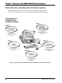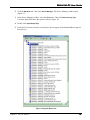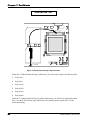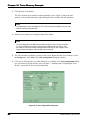
1
ICE Technology Nohau Brand Emulator
EMUL196–PC™
User Guide
Edition 1, June 6, 2001
© 2001 All rights reserved worldwide.
EMUL196–PC User Guide
Contents
About This Guide
x
Downloading EMUL196–PC Product Documentation
x
Overview of the EMUL196–PC Emulator System
High-Speed Parallel (HSP) Box
2
Universal Serial Bus (USB) Box
2
PC Plug-In/Industry Standard Architecture (ISA)
3
Low-Cost Industry Standard Architecture (LC–ISA)
User Interface
1
3
3
Quick Start for Installing Your Emulator System
Quick Start for Installing the Hardware
4
5
Installing and Configuring the Seehau Software
Configuring the Seehau Software
7
7
Running the Configuration Software
8
Purchasers of Emulator and Trace Boards
10
Configuring Address Settings With Windows Operating Systems 11
Configuring Address Settings for the Emulator and Optional Trace Board
Information about Windows NT Installation
Known Device Driver Conflicts
11
11
Configuring Address Settings with Windows 95/98
Configuring Address Settings with Windows NT
Configuring Address Settings with Windows 2000
Edition 1, June 6, 2001 ©
12
13
16
i
11
Installing and Configuring the Emulator Board
Installing the Emulator Board
22
Emulator Installation Instructions
Setting the I/O Address Jumpers: J2
Typical PC I/O Addresses
Addressing Examples
Header JP1
Header J4
23
23
23
24
24
24
Installing the Emulator Board into the ISA Slot
Shadow RAM
266
Installing and Configuring the Trace Board
Hardware Description
27
27
External Inputs and Controls
Tracing Overview
Trace Modes
28
30
30
Trace Window
31
32
Trace Configuration
Trace Setup Tab
33
33
Trigger / Filter ConfigurationTabs
Entering Addresses and Data
Opcode Trigger Mode
35
36
36
Data Trigger Mode
37
Data to Trigger On
37
Other Controls for Trace Configuration
ii
27
27
Installation Instructions
I/O Address
25
25
Quick-Save Settings
Trace Menu
21
38
EMUL196–PC User Guide
EMUL196–PC User Guide
Accessories and Adapters
Type of Adapters
39
39
Verifying the Orientation of Your Adapter
Creating a Shortcut to PicView
39
40
Installing and Configuring the Pod Board
Overview
41
41
Features Common to All Pod Boards
Stack Pointer
41
41
Indicator Lights
42
How to Simultaneously Stop Code Execution on Two Emulators 42
Trace Input Pins
42
Resource Selection
Power
XTAL
42
43
43
Microcontroller
Clip-Over Adapter
43
44
Summary of Hardware Configuration
44
Memory Map Configuration Requirements
Enough Emulator Memory?
45
Internal Addressing or Single-Chip Mode
45
Replacing Ports: POD196–KR/NT and CA/CB
Port Replacement Unit (PRU)
Edition 1, June 6, 2001 ©
45
46
Program Performance Analyzer (PPA)
Code Coverage
44
46
46
iii
Pod Boards
47
POD196–KC / KD
Overview
Dimensions
47
47
47
Emulation Memory
Wait States
48
48
Headers and Jumpers
48
Procedure to Test
53
Memory Mapping
53
Hardware Breakpoint Setup
54
Helpful Hints for Compiling
Download Procedure
POD196–KR / NT
Overview
Dimensions
55
56
56
56
NMI Pin (KR/NT only)
PRU
54
57
57
Emulation Memory
57
Headers and Jumpers
57
KR/NT Ready Functionality
POD196–NP / NU
Overview
Dimensions
64
64
64
Emulation Memory
Wait States
61
65
65
Headers and Jumpers
66
Symbols in the Trace Window
71
Mapping Memory Using Chip Selects
Port Replacement Unit
Overview
72
74
74
When to Use a Port Replacement Unit
Installing the PRU
74
75
PRU Headers and Jumpers
75
PRU Special Function Registers
76
Design Limitations and Silicon Bugs—PRU
PRU Header JP2—Accessing P3, P4 and P5
iv
78
78
EMUL196–PC User Guide
EMUL196–PC User Guide
Starting the Emulator and Seehau Software
Hardware Connection
Starting Seehau
83
84
Time Program Example
Example Program
85
85
Watching Data in Real-Time with Shadow RAM
Trace Memory Example
Overview
89
89
Saving the Configuration
91
Shutting Down Seehau
93
Steps to Shut Down Seehau
93
Important Software and Hardware Notes
Appendix A. Troubleshooting
94
95
95
Stack Pointer
96
HSP/USB Box
97
Debugging the Parallel Port
Windows NT Users
99
Windows 9x Users
99
Windows 2000 Users
ISA
86
89
Running the Example
Overview
83
99
99
104
Edition 1, June 6, 2001 ©
v
If the Emulator Does Not Start When Connected to
the Target System
105
Board I/O Addresses
105
Emulator Configuration Utility Screen
PWR and XTAL Jumpers
I/O on Address Pins
106
107
Chip Configuration Bytes (CCBs)
Enough Memory
106
107
107
The Stack Pointer
107
Interrupt Vectors
108
Nonmaskable Interrupt (NMI) Pin (KR/NT only)
Buswidth (CA/CB only)
Single-Chip Mode
108
109
Sample User Program
Appendix B. ISO–160
PLCC–52–ISO
109
111
111
EMUL196/ISO-160
111
SAMTEC/SSQ–117–03–GD
Appendix C. Compilers
Overview
Tasking
113
115
115
115
Compiler Notes
Assembler Notes
IAR
115
115
116
Appendix D. Emulator / Trace Address Examples
vi
108
117
EMUL196–PC User Guide
EMUL196–PC User Guide
Appendix E. Discontinued Pod Boards
POD196–CA / CB
Overview
Dimensions
121
121
122
Emulation Memory
INST
122
122
Port Replacement Unit (PRU)
122
Nonmaskable Interrupt (NMI) Pin
Headers and Jumpers
POD196–EA
Overview
Dimensions
126
134
134
134
Emulation Memory
Addressing RAM
135
135
8-Bit Mode and BHE Mode
Headers and Jumpers
Memory Mapping
POD–196LC–KR/NT
141
142
142
143
143
Emulation Memory
Headers and Jumpers
Glossary
140
141
Port Replacement Unit (PRU)
Dimensions
136
136
Symbols in the Trace Window
Overview
123
123
87C196CB Bondout Errata
PRU
121
143
143
147
Index
Sales Offices, Representatives and Distributors
Edition 1, June 6, 2001 ©
vii
vii
Product Notes
European CE Requirements
Nohau has included the following information in order to comply with European CE requirements.
User Responsibility
The in-circuit debugger application, as well as all other unprotected circuits need special mitigation to ensure Electromagnetic Compatibility (EMC).
The user has the responsibility to take required measures in the environment to prevent other
activities from disturbances from the debugger application according to the user and installation
manual.
If the debugger is used in a harsh environment (field service applications for example), it is the
user’s responsibility to control that other activities cannot be disturbed in such a way that there
might be risk for personal hazard/injuries.
Special Measures for Electromagnetic Emission Requirements
To reduce the disturbances to meet conducted emission requirements it is necessary to place a
ground plane on the table under the pod cable and the connected processor board. The ground
plane shall have a low impedance ground connection to the host computer frame. The insulation
sheet between the ground plane and circuit boards shall not exceed 1mm of thickness.
Warnings
To avoid damage to the pod or to your target, do not connect the pod to your target when
the pod or target power is on.
When powering up, always power up the emulator first followed by the target system.
When powering down, power down the target system first followed by the emulator.
Failing to do so can cause damage to your target and/or emulator.
Do not apply power to your system unless you are sure the target adapter is correctly
oriented. Failing to do so can cause damage to your target and/or emulator.
When using the pod with a target, disable all pod resources that are duplicated on the target. Failure to disable the pod’s resources can damage the pod or the target or both. This
includes the MCU, the serial port, RAM, crystal, and, particularly, the power supply. If
using the clip to attach to the target, remove the MCU from the pod.
When installing a controller into a pod, never press on the chip body. Press only on the
carrier or cover. Pressing on the chip can bend pins and cause short circuits.
viii
EMUL196–PC User Guide
EMUL196–PC User Guide
Minimum System Requirements
CAUTION
Like all Windows applications, the Seehau software requires a minimum amount of free operating system resources. The recommended amount is at least 40%. (This is only a guideline. This
percentage might vary depending on your PC.) If your resources are dangerously low, Seehau
might become slow, unresponsive or even unstable. If you encounter any of these conditions,
check your free resources. If they are below 40%, reboot and limit the number of concurrently
running applications. If you are unable to free at least 40% of your operating system resources,
contact your system administrator or Nohau Technical Support at [email protected].
The following are minimum system requirements:
• Pentium 200 (Pentium II or faster is recommended)
• Single-Processor System
• Windows 95, 98, NT, 2000, or 2000 ME
• Random Access Memory (RAM)
–
–
For Windows 95/98: 64 MB
For Windows NT/2000/2000ME: 128 MB
• Two ISA slots in your PC if the optional trace board is purchased, otherwise purchase the
HSP or USB box.
Edition 1, June 6, 2001 ©
ix
About This Guide
The EMUL196–PC User Guide describes how to use the EMUL196–PC emulation system with
the Seehau graphical user interface. This guide is intended for both novice and advanced users.
The EMUL196–PC is a PC-based emulator for the Intel 80C196 family of microprocessors.
This guide helps you to get started with the basics of setting up, configuring, and running the
Seehau software and the emulator. If you have any questions contact Nohau Technical Support
at [email protected] or refer to the Sales Offices, Representatives and Distributors list at the
end of this guide.
Online context sensitive Help is also available from the Seehau software by pressing the F1 or the
Help keys, depending on the type of keyboard you have.
The EMUL196–PC User Guide introduces the following tasks:
•
Installing and Configuring the Seehau Software
•
Installing and Configuring the Emulator
•
Installing and Configuring Trace Boards
•
Types of Adapters
•
Installing and Configuring Pods
•
Starting the Emulator and Seehau Software
•
Time Program Examples
•
Trace Memory Example
•
Macro Example
•
Shutting Down Seehau Software
•
Troubleshooting
•
Hex Pin Addressing
• Glossary
Downloading EMUL196–PC Product Documentation
To download an electronic version of this guide, do the following:
1. Open Nohau’s home page at www.nohau.com.
2. Click Publications.
3. Click Nohau Manuals.
4. Scroll down to EMUL196–PC. Then select EMUL196–PC to download a PDF version
of this guide.
x
EMUL196–PC User Guide
EMUL196–PC User Guide
Overview of the EMUL196–PC
Emulator System
The basic hardware for the EMUL196–PC emulator system includes the following:
• Emulator board—plugs into an ISA slot inside the PC, HSP or USB box.
• Standard or Data trace board (optional)—plugs into an ISA slot inside the PC, HSP or USB
box and connects to the emulator board through two short ribbon cables.
• Pod board—the device that allows you to emulate the device under development.
• Five-foot twisted-pair ribbon cable—connects the emulator and pod.
• Combination 25-pin to 50-pin cable (part number CBL-A-LC25/50) for the LC–ISA only.
• Target adapter—allows you to connect the pod board to your target system.
To connect to your target system, the pod board usually requires an adapter. To determine the
adapter board that your pod requires, check the price list, your representative or Nohau Technical
Support at [email protected].
The EMUL196–PC emulator consists of an emulator and a pod board. The pod board typically
requires an adapter to connect to your target system. An optional trace board can be added to all
systems except for the low-cost systems (LC–ISA) for advanced tracing capabilities. Four system
configurations are available to suit your needs:
• High-Speed Parallel (HSP) Box connects to the parallel printer port. See the following
“High-Speed Parallel (HSP) Box” section.
• Universal Serial Bus (USB) Box. See the following “Universal Serial Bus (USB) Box”
section.
• PC Plug-In/Industry Standard Architecture (ISA). See the following “PC Plug-In/Industry
Standard Architecture (ISA)” section.
• Low-Cost Industry Standard Architecture (LC–ISA). See the following “Low-Cost Industry
Standard Architecture (LC–ISA)” section.
You can configure the emulator hardware to your requirements with various jumpers. For details
on configuring your emulator board, refer to Chapter 3, “Installing and Configuring the Emulator
Board.” For details about the optional trace board, refer to Chapter 5, “Installing and Configuring
the Trace Board,” or go to Seehau Help in the software.
Edition 1, June 6, 2001 ©
1
Chapter 1. Overview of the EMUL196–PC Emulator System
Figure 1. HSP Box Connected to a Pod Board and Laptop Computer
High-Speed Parallel (HSP) Box
The HSP box lets you use the in-circuit emulator and optional trace board where no ISA slots are
available. If purchased as a set, Nohau company personnel will mount the emulator board, HSP
card, and optional trace board in the HSP box chassis. The optional trace board connects to the
emulator board through two ribbon cables. The pod board connects to the emulator board in the
HSP with a five-foot ribbon cable. The HSP card connects to the PC’s parallel printer port. This is
one of the most portable methods of connection when used with a laptop computer and gives you
full trace capability.
Universal Serial Bus (USB) Box
When using a laptop computer, the USB box provides one of the most portable methods of connection and allows for full trace capability. A USB port is an external peripheral interface standard
for communication between a computer and external peripheral over a cable that uses biserial
transmission. You can use the USB box to run the in-circuit emulator and optional trace board
when ISA slots are unavailable in your computer.
Note
When using the USB option, you must install the Seehau software first before
connecting the Nohau hardware. This allows the computer to recognize the
proper driver for the hardware. The USB option is not supported by Windows NT.
It is anticipated that the USB option will eventually replace the parallel port interface.
2
EMUL196–PC User Guide
EMUL196–PC User Guide
PC Plug-In/Industry Standard Architecture (ISA)
The emulator ISA board is plugged into an ISA slot in your PC, USB or HSP and is connected
with a five-foot cable to a device-dependent pod board. The optional trace board can also be
plugged into the PC, HSP or USB box and is connected to the emulator board through two short
ribbon cables.
Note
If the optional trace board were purchased for PC installation, you would need to
ensure that your computer motherboard has at least two open ISA slots or you will
need to purchase the HSP or USB box.
Low-Cost Industry Standard Architecture (LC–ISA)
The EMUL/LC–ISA board is an 8-bit PC card that fits into any ISA slot in your PC. This board
must be connected to a pod board to operate. Low cost emulators do not have Shadow RAM, or
provision for a real-time trace (or the ability to add a trace board). The maximum frequency is set
by the frequency limit on the pod board. The connection for the board to pod is through a 25-pin
connector from the board to a 50-pin connector to the pod (part number CBL–A–LC25/50).
User Interface
The emulator is configured and operated by the Seehau user interface. Seehau is a high-level
language user interface that allows you to perform the following tasks:
• Load, run, single-step and stop programs based on C or Assembly code.
• Set triggers and view trace (with optional trace board).
• Modify and view memory contents including Special Function Registers (SFRs).
• Set software and hardware breakpoints.
• Analyze code with Program Performance Analysis (PPA).
Edition 1, June 6, 2001 ©
3
Chapter 1. Overview of the EMUL196–PC Emulator System
Quick Start for Installing Your Emulator System
The following illustration shows the major steps for installing and configuring the
EMUL196–PC. For details, refer to the chapter and/or pages referenced in each step.
Figure 2. Steps for Installing and Configuring the EMUL196–PC and Seehau Software
4
EMUL196–PC User Guide
EMUL196–PC User Guide
Quick Start for Installing the Hardware
The following illustration shows the major steps for installing the EMUL196–PC hardware.
Figure 3. Steps for Installing the EMUL196–PC Hardware
Edition 1, June 6, 2001 ©
5
Chapter 1. Overview of the EMUL196–PC Emulator System
6
EMUL196–PC User Guide
EMUL196–PC User Guide
Installing and Configuring the
Seehau Software
To install the Seehau software, do the following:
1. Locate your Seehau CD and insert the CD into your CD ROM drive. The installation process
will start automatically.
2. Follow the instructions that appear on your screen.
Note
If the installation does not start automatically, you probably have your Windows
Autorun feature disabled. You will then need to use Windows Explorer and navigate
to the CD root directory or right-click on the drive where the CD is located. If you
navigate to the root directory find Autorun.exe and double-click on it. If you
right-click on the drive where the CD is located, select AutoPlay to start the
install process.
Configuring the Seehau Software
When first started, Seehau loads a configuration file called Startup.bas This file is created by the
Seehau Configuration Program, which stores Startup.bas in the following directory:
C:\Nohau\Seehau196\Macro
The Seehau software automatically starts Seehau Config if it does not find the startup file.
You do not need to have the emulator connected to the PC to run the Seehau Configuration Program. However, for the Seehau regular executable to operate, the emulator must be connected with
the jumpers set correctly.
Get familiar with the emulator in stand-alone mode (not connected to a target system) or the demo
mode before connecting to a target hardware system. The added complications of the target hardware might cause you problems at this time. Once you have gained some skills at operating the
emulator, then connect to your target. To operate in Demo mode select Start/Programs/Seehau
196/Demo.
Edition 1, June 6, 2001 ©
7
Chapter 2. Installing and Configuring the Seehau Software
Figure 4. Emulator Configuration (Communications) Dialog Box
Running the Configuration Software
1. Click the Seehau Config icon on your desktop. You do not need the emulator connected
at this time.
2. Enter the correct settings as shown in the Emulator Configuration dialog box (Figure 4).
WARNING
To avoid damage to the pod or to your target, do not connect the pod to your target when pod or
target power is on.
3. Change the settings as indicated. Figure 4 shows the settings used if you are using the HSP
box. Figure 5 shows the settings for the ISA card. You enter the address of your computer’s
internal communication link in the Emulator Board Address text box. For the ISA card, the
most common address is 200. If the computer has a game port or joy stick, it is typically located at address 201H. If this is the case, you will need to change the address of the emulator
board to an unused hardware address. You can change this setting on the board. If you are using the HSP, this address is not applicable. The HSP box uses address 378 which, represents
the LPTI port on your PC.
8
EMUL196–PC User Guide
EMUL196–PC User Guide
Figure 5. Emulator Configuration Dialog Box for the ISA
Figure 6. Hardware Configuration
Edition 1, June 6, 2001 ©
9
Chapter 2. Installing and Configuring the Seehau Software
4. When all the information has been entered, click Next to open the screen as shown in
Figure 6. For information on the other settings, refer to the Intel handbook under the “Chip
Configuration Register” section.
5. The uP Clock is the internal CPU clock. This setting is used only for the calculation of the
trace timestamp. It has no effect on the operating speed of the emulation controller. The time
entered here should be the internal processor speed (not necessarily the crystal speed).
6. Click Next to enter the data. Click Yes at the Are you finished? prompt.
7. The Seehau Configuration Program creates Startup.bas and Seehau is now configured to run
your emulator.
8. The Seehau Configuration Program closes.
If you have completed these steps without any errors, you are ready to run the Seehau user interface after you have connected and powered up the EMUL196–PC emulator.
WARNING
The target power must never be on when the pod is powered off. To avoid damage, power the pod
and target on and off in the following sequence. To power up: (1) Power on the pod, then (2) Power
on the target. To power down: (1) Power off the target, then (2) power off the pod.
Purchasers of Emulator and Trace Boards
If you are purchasing the emulator board and the trace board, you might want to consider the
following points:
• You will need a PC with at least two ISA slots. These slots should be close enough to allow
you to connect the short ribbon cables that connect the boards or consider purchasing the HSP
or USB box.
• It will be easier to connect the short ribbon cables before installation. Waiting until the
boards are already installed can result in scraped and/or bloody knuckles due to the
restricted work area.
• If you purchase the trace board after the emulator board, you should consider removing the
emulator board, making the ribbon connections, and then installing the boards together.
10
EMUL196–PC User Guide
EMUL196–PC User Guide
Configuring Address Settings with Windows
Operating Systems
The following applies to all Windows operating systems:
• Default Address Ranges:
–
–
Emulator Board: 200H
Trace Board: 208H
• Default Address Settings for the HSP Box:
No address conflict is possible when installing the HSP box with any Windows operating system.
Use the default address ranges (listed above).
Skip to “Installing Emulator Boards” later in this chapter.
Configuring Address Settings for the Emulator and Optional
Trace Board
The following sections provide details about configuring address settings for the emulator and
optional trace board for each Windows operating system. Refer to the section that covers your
specific operating system.
Information about Windows NT Installation
When installing under Windows NT you will be changing the registry and installing our kernel
mode driver. You must do this from an account with Administrator privileges.
One of the causes of the message Incorrect Parameter either in the system log or from the Devices
application is that there might be a device already installed with the address given for the emulator.
Known Device Driver Conflicts
Nohau is aware of potential device driver conflicts with certain network cards running on
Novell/Netware networks. Problems have been reported with both 3COM ISA network cards
and some Novell network cards. Most of these problems have been experienced when running
Windows NT or Windows 2000 operating systems.
Possible Symptoms
•
•
When starting Seehau, communication with the network stops. (You will be unable to access
resources on the network.)
Seehau will not start.
A possible solution might be to change your network card. Nohau Technical Support has not
tested all network cards, although some customers have reported that the following network cards
have resolved this conflict:
•
•
•
Intel Ether Express Pro 10/100 ISA
3COM Etherlink III (905B or later) 10/100 PCI
Bay Networks NetGear FA310TX 10/100 PCI
Edition 1, June 6, 2001 ©
11
Chapter 2. Installing and Configuring the Seehau Software
Configuring Address Settings with Windows 95/98
Checking Your PC for Default Address Conflicts
1. Click the Start menu, and select Settings.
2. Click Control Panel.
3. Double-click System. The Systems Properties dialog box opens.
4. Click the Device Manager tab.
5. Click Properties.
6. Click Input/Output. Scroll the contents of the window to verify that no device is listed within
that range.
Alternative Addressing
If you see a device present in the default address range for your emulator or trace board, do the
following:
1. Beginning at the address 200H, scroll down to look for an unused address range:
–
–
–
Recommended for emulator boards are addresses 200H, 210H, and 240H.
Recommended for trace boards are addresses 208H, 218H, and 248H.
The trace board address must always be at least 8H above the emulator board
(i.e., 200/208, 210/218, 240/248).
2. When you locate an unused address range, make a note of the base address of the range for use
when configuring Seehau.
3. Refer to Appendix D, “Emulator/Trace Address Examples” to reconfigure the base address of
your board.
The base address must be an even multiple of 10 (such as 200 or 210). If you have to change
the address of the emulator or trace board, be sure to change both the board jumpers and the
jumper settings in the software.
Figure 7. System I/O Resources
12
EMUL196–PC User Guide
EMUL196–PC User Guide
Configuring Address Settings with Windows NT
•
First, check your administrative privileges.
• Then check your PC for default address conflicts.
Checking Administrative Privileges
1. Click the Start menu, and select Programs.
2. Select Administrative Tools, and click User Manager. The User Manager dialog box opens
(Figure 8).
3. In the bottom half of the dialog box, double-click Administrators. The Local Group Properties
dialog box opens displaying a list of login names (Figure 9).
Figure 8. User Manager Dialog Box for Windows NT
Figure 9. Local Group Properties Dialog Box for Windows NT
Edition 1, June 6, 2001 ©
13
13
Chapter 2. Installing and Configuring the Seehau Software
4. Look for your login name in the list of names. If your login name is not present, you are not set
up with administrative privileges. Contact your System Administrator to update your privileges or give you the administrator’s password.
Checking Your PC for Default Address Conflicts
1. Click the Start menu, and select Programs.
2. Select Administrative Tools, and click Windows NT Diagnostics. The Windows NT
Diagnostics window opens (Figure 10).
3. Click the Resources tab.
4. Click I/O Port.
5. Check the I/O resources listed to verify that no device appears in a default address range.
Alternative Addressing
If you see a device present in the default range for your emulator or trace board, do the following:
1. Beginning at the address 200H, scroll down to look for an unused address range:
–
–
200H, 210H, or 240H for the emulator board.
208H, 218H, or 248H for the trace board.
Figure 10. NT Diagnostics Window
14
EMUL196–PC User Guide
EMUL196–PC User Guide
2. When you locate an unused address range, make a note of the base address of the range for use
when configuring Seehau.
3. Refer to Appendix D, “Address Examples” to reconfigure the base address of your board.
Driver Troubleshooting
• If you get a Service or driver failed error message when rebooting, you probably have a
resource conflict.
• If you get a create file failed error message upon execution, the device driver did not
properly start.
Nohau196 Device Driver
After installation, Windows NT Diagnostics will show the Nohau196 device driver present in the
upper I/O range (FFxx). After launching Seehau, the driver is reassigned to the actual address
ranges. In the Control Panel Devices window (Figure 11), you will see three columns: Device,
Status, and Startup.
• Device: lists the Nohau device driver
• Status: displays Started
• Startup: displays Automatic
Figure 11. Control Panel Devices Window
Edition 1, June 6, 2001 ©
15
15
Chapter 2. Installing and Configuring the Seehau Software
Configuring Address Settings with Windows 2000
•
•
First, check your administrative privileges.
Then check your PC for default address conflicts.
Checking Administrative Privileges
1. Click the Start menu, and select Settings. Click Control Panel.
2. From the Control Panel, double-click Users and Passwords. The Users and Passwords
window opens (Figure 12).
3. Click the Advanced tab. Now click the Advanced button. The Local Users and Groups
window opens (Figure 13).
Figure 12. Users and Passwords Window
Figure 13. Local Users and Groups Window
16
EMUL196–PC User Guide
EMUL196–PC User Guide
Figure 14. Local Users and Groups Window with Groups Folder
4. Click the Groups folder located in the left region of the window beneath Local Users
and Groups.
5. Double-click the Groups folder. A list of groups appears in the right region of the window
(Figure 14).
6. Double-click Administrators. Your user name should be listed.
Note
If you are not an administrator, ask your System Administrator to add you to this list.
Figure 15. Administrator Dialog Box
Edition 1, June 6, 2001 ©
17
Chapter 2. Installing and Configuring the Seehau Software
Checking Your PC for Default Address Conflicts
1. Right-click the My Computer icon on your desktop, and select Properties. The System
Properties window opens (Figure 16).
Figure 16. System Properties Window
Figure 17. Device Manager Window
18
EMUL196–PC User Guide
EMUL196–PC User Guide
2. Click the Hardware tab. Then click Device Manager. The Device Manager window opens
(Figure 17).
3. In the Device Manager window, select the View menu. Then click Resources by Type.
A window opens that shows the system resources (Figure 18).
4. Double-click Input/Output (I/O).
5. Check the I/O resources listed to verify that no device appears in the default address range for
these devices.
Figure 18. System Resources
Edition 1, June 6, 2001 ©
19
Chapter 2. Installing and Configuring the Seehau Software
Alternative Addressing
If you see a device present in the default address range for your emulator or trace board, do the
following:
1. Beginning at the address 200H, scroll down to look for an unused address range:
–
–
200H, 210H, or 240H for the emulator board.
208H, 218H, or 248H for the trace board.
2. When you locate an unused address range, make a note of the base address of the range for use
when configuring Seehau.
3. Refer to Appendix D, “Address Examples” to reconfigure the base address of your board.
Driver Troubleshooting
For details, see Appendix A, “Troubleshooting Tips.”
• If you get a Service or driver failed error message when rebooting, you probably have a
resource conflict.
• If you get a create file failed error message upon execution, the device driver did not properly
start. Review the steps in this section again. You can use Windows 2000 System Properties to
recheck that your port address has no conflicts.
Nohau196 Device Driver
To verify that the Nohau196 device driver is properly installed, do the following:
1. From the Start menu, select Programs. Select Accessories, then System Tools.
2. Click System Information. The System Information window opens.
3. Double-click the Software Environment folder.
4. Double-click the Drivers folder. A list of active drivers appears. Refer to the Name column
and scroll down to nohau196.
5. Verify the driver is running. In the State column, you should see the word Running. In the
Status column, you should see OK.
20
EMUL196–PC User Guide
EMUL196–PC User Guide
Installing and Configuring the
Emulator Board
1. If you are using the ISA card inside the PC, verify that the jumpers on the board are set for
200H (the default address). If the computer has a game port or joy stick, it is typically located
at address 201H. If this is the case, you will need to change the address of the emulator board
to an unused hardware address.
2. If you have the HSP box, connect the parallel cable to the parallel port of the PC or laptop.
Also, connect the 5-volt power supply. The default parallel port is LPT1, located at the hardware address 378H within the PC.
3. Connect the five-foot ribbon cable from the emulator board to the pod.
Key
Key Slot
Figure 19. Connecting the Emulator to Your Pod Board with the Ribbon Cable
Note
The connectors of the ribbon cable are identical so it does not matter which end is
connected to the pod or the emulator board. Although the ribbon cable connecting
the emulator to the pod board is keyed, it is possible to force the key on the conector the wrong way. Caution should be used when making the connection to ensure
that the key and slot line correctly.
Although not part of the emulator board, you might want to ensure the following steps as you hook
up and configure the emulator board.
1. Verify the pod is stand-alone (not connected to the target), and that the power jumper is inserted and the crystal jumpers are set for internal crystal.
2. There are four address jumpers: EA16, EA17, EA18, and EA19. The settings for these jumpers
must match the number of address lines selected when the hardware screen was configured.
Edition 1, June 6, 2001 ©
21
Chapter 3. Installing and Configuring the Emulator Board
REV. D
JP2
JP3
Pin 1
NOHAU CORP.
EMUL-PC/E
S/N
J4
A3
JP1
A9
J2
Figure 20. Rev. D Emulator Board
Installing the Emulator Board
The EMUL196–PC emulator board supports the following pod boards for different members of the
Intel 80C196 microcontrollers:
•
•
•
POD196–KR/NT
POD196–NP/NU
POD196–KC/KD
Note
Pods 196–CA/CB, 196–NP, and 196–EA have been discontinued. For information
about these pod boards, see Appendix E, “Discontinued Pod Boards.”
As Intel introduces other members of the 80C196 family of microcontrollers, corresponding pod
boards will be introduced and supported by EMUL196–PC. Call Nohau Technical Support for the
current list of available pod boards and supported controllers.
The EMUL196–PC emulator board is an 8-bit PC card that fits into any ¾ length slot. It contains
64K, 256K, or 1 MB of Shadow RAM, bus interface logic, trace board support logic, and the logic
needed to communicate with the pod. The jumpers on the emulator board control two things:
22
•
The address used to communicate with the Host PC.
•
The maximum communication rate of the target.
EMUL196–PC User Guide
EMUL196–PC User Guide
Emulator Installation Instructions
Setting the I/O Address Jumpers: J2
Each pair of pins in the address header J2 represents one bit in the 10-bit address. Address bits
0, 1, and 2 represent addresses within the eight consecutive addresses, and they do not have pin
pairs to represent them. This leaves six address bits (pin pairs) to set with jumpers: A3 through A9.
Shorting two pins represents a zero in the address. A pair of pins with no jumper represents
a one.
The emulator board address jumpers have been factory preset to 200H for a typical system. The
following table shows how a typical system uses its address locations. If your system is presently
using location 200H, you must find an alternate address location and make appropriate changes to
the jumpers and software. If your emulator board is in an external HSP/USB box, you should use
the default address regardless of the I/O address being used in the computer.
Typical PC I/O Addresses
Hex Location
Typical Use
000 – 0FF
Used by system
1F0 – 1F8
Fixed disk
200 – 207
Game adapter
210 – 213
Expansion unit
278 – 27F
Parallel printer Port 2
2F8 – 2FF
Secondary asynchronous printer adaper
300 – 31F
Prototype card
320 – 323
Fixed disk controller
360 – 36F
Reserved
378 – 37A
Printer adapter
380 – 38F
Alternate binary synchronous communications adapter, SDLC adapter
3A0 – 3AF
Primary binary synchronous communications adapter
3B0 – 3BF
Monochromatic display and printer adapter
3C0 – 3CF
Reserved
3D0 – 3DF
Color/graphics monitor adapter
3F0 – 3F7
Floppy disk controller
3F8 –3FF
Primary asynchronous printer adapter
If the current emulator board address conflicts with any other hardware, find free address space
between 210 and 3FFH. The emulator board requires eight consecutive addresses. If you change
the address and/or memory jumpers, the software address settings must also be changed.
Edition 1, June 6, 2001 ©
23
Chapter 3. Installing and Configuring the Emulator Board
PC Bus Address
Pin labels
A3
200 Hex
A9
A3
208 Hex
A9
Jumper Settings
Factory Default
PC Bus Address
Pin labels
A3
300 Hex
A9
A3
3F8 Hex
A9
Jumper Settings
Figure 21. Emulator I/O Address Header J2
Addressing Examples
Figure 21 shows the four different address configurations for the emulator board.
Header JP1
This header is not currently implemented on EMUL196–PC. Leave the jumper in the default position, between Pins 3 and 4.
Header J4
The following paragraph applies only to emulator boards with 1 MB of Shadow RAM. Emulators
with less than 1 MB of Shadow RAM must leave the jumper between Pins 2 and 3.
On some 8xC196 controllers, the same CPU pin can carry a port E I/O signal, or AD19, an address
bit. Target designs with 512K or less of RAM or ROM can use the AD19/EP.3 pin to carry an I/O
signal instead of the address signal. For emulator boards with 1 MB of Shadow RAM, insert the
header between Pins 1 and 2. This is the default position for 1 MB Shadow RAM emulator boards.
If your emulator board has 1 MB of Shadow RAM, and Pin AD19EP.3 carries an I/O signal, then
short Pins 2 and 3 of Header J4. Do not change the jumper for Header J1.
WARNING
Always turn on the PC before powering to the target. Always turn off the target power before turning off the PC power. Always turn off the PC before connecting or disconnecting the ribbon cable to
the emulator or pod board, and before connecting the pod to the target. Not doing so could damage
the CPU, the emulator, the pod or the target.
24
EMUL196–PC User Guide
EMUL196–PC User Guide
Installing the Emulator Board into the ISA Slot
After the jumpers are set, do the following with the PC power off:
1. Remove the PC cover.
2. Insert the emulator board into any free slot.
3. Close the PC cover.
4. Connect the ribbon cable to the emulator board.
5. Connect the pod to the ribbon cable.
Shadow RAM
The EMUL196–PC emulator board contains either 64K, 256K, or 1 MB of static RAM used to
shadow or duplicate the contents of the target RAM. Every time the CPU generates a WRITE bus
cycle while running the target application, the pod captures the address/data pair and the emulator
board writes that data to the same address in Shadow RAM. The Seehau application can simultaneously read Shadow RAM. This allows the software to display values written by the application
without interrupting emulation.
Note
Shadow RAM will capture external data writes while you are running your code.
Shadow RAM will not capture the bus activity while the pod is executing monitor
code. Loading code, filling memory, and editing registers will not update Shadow
RAM.
Notice the emulator board has 64K of Shadow RAM, and the application data area RAM is larger.
The emulator board has 64K of Shadow RAM. If your microcontroller accesses addresses above
64K, the data WRITE address will be masked off to 16 bits when reaching the Shadow RAM. The
Shadow RAM address logic strips off the bits above bit 15. The Shadow RAM address 100H will
be modified by WRITEs to application RAM addresses 100H, 10100H, and 20100H. Similarly, if
the emulator has 256K of Shadow RAM, WRITEs to application RAM addresses 100H, 40100H,
and 80100H will all update the same Shadow RAM byte (at address 100H). This is true for emulation RAM, RAM on the target, or even memory-mapped I/O devices. Ordering an emulator
board with 256K of Shadow RAM will minimize the amount of overlaid RAM. However, targets
that have more than 256K of RAM, overlaying will still be possible. Ordering an emulator board
with 1 MB of Shadow RAM will eliminate this problem for all 8xC196 applications.
Edition 1, June 6, 2001 ©
25
Chapter 3. Installing and Configuring the Emulator Board
Quick-Save Settings
Due to the instability of PCs and operating systems, it is important to take precautions after setting
up your hardware and software. Rather than wait until you have finished doing your tests on the
target system you might want to save the emulator settings to avoid unnecessary repetition in case
of system failure. The quick way to avoid this problem is to do the following:
1. To save the emulator configuration, click the Config option and select Environment.
2. From the Environment Configuration menu, check the Use Start-up Dialog? (this prompts
you to select the preferred startup file when selected) under the Preferences tab. This option
is located in the Miscellaneous section.
3. Select Apply or OK. The Environment Configuration dialog box will close.
4. Exit from the Seehau software.
5. The Save Settings dialog box opens where you can choose the filename for the newly created
macro. Enter a filename of your choosing and click Save.
The macro is ready to use and will accurately recreate your emulator configuration settings.
26
EMUL196–PC User Guide
EMUL196–PC User Guide
Installing and Configuring the
Trace Board
Hardware Description
The trace board is a full length ISA-style bus card and contains the RAM needed to record a
record of the data accessed and instructions executed. The emulator board has the logic and connectors necessary to support the trace board. It can occupy any 8- or 16-bit slot as long as the two
ribbon cables can reach from the emulator card to the trace card. When inserted into a 16-bit slot,
it connects with the additional power and ground lines in the other connector on the motherboard.
The card includes 104 bits of RAM for each trace record. There are two types of trace boards for
the EMUL196–PC: standard and data. Standard trace boards are available with 32K of trace memory, data trace boards are available with either 128K or 512K of trace memory.
Installation Instructions
The trace board includes three connectors on the back for inputting and outputting signals. Figure
23 shows how the connectors for the DB-25 connector and the two BNC connectors are wired.
I/O Address
Like the emulator, the trace board uses eight consecutive I/O addresses for communicating with
the PC. The jumpers on the card are set at the factory to allow the trace board to use the I/O addresses that start at 208H. Confirm either that these addresses are available on your PC or find
eight consecutive free addresses and set the address jumpers on Header J1 accordingly. On the
trace board, A3 is on the right; on the emulator board, A3 is on the left. (See the examples in
Figure 21 and Figure 22.)
Figure 22. Trace Board I/O Address Header J1
Edition 1, June 6, 2001 ©
27
Chapter 4. Installing and Configuring the Trace Board
After the trace board address jumpers are set, do the following:
1. Turn off the PC power or HSP/USB box power, remove the cover, and slide the board into
the chosen ISA slot (the ISA slots must be next to each other). Make sure the board is fully
inserted. There are two identical ribbon cables. Due to the length and shape of the cables, it
is impossible to attach both cables to the incorrect connector.
Note
It might be easier to remove the emulator board from the chassis and attach the
cables before reinserting the boards into their respective slots. The tightness around
the boards and the pins can result in skinned or bloody knuckles if not careful.
2. Make sure the pins are fully inserted into the connectors so there are no exposed pins, there
are no twists in either cable, and the cables do not cross. Be certain the connectors are not offset vertically or horizontally. The most common error is to insert only one row of pins into the
connector. This can damage either of the boards. Double-check all four connectors for any exposed pins before continuing.
3. After the ribbon cables are attached, close the PC or HSP/USB box cover, power up the PC or
HSP/USB box, and start Windows.
4. Start the Seehau196 program.
5. Verify that the Seehau196 configuration is set up to recognize the trace board. This is done in
the Seehau196 Configuration Program.
6. Verify that Trace Type indicates Trace (Yes), and the I/O address is correct. This address box
needs to contain the same address as the jumpers in Header J1 as mentioned previously.
Note
If the hex address was changed for the emulator board, the hex address for the
trace board must be changed accordingly.
External Inputs and Controls
The trace board records eight external digital inputs with every bus cycle. These signals are input
through the DB-25 (also called a D connector) connector on the back of the trace board. To simplify providing these signals to the trace board use the color-coded set of micro-clips provided
with the trace board. (The 25-conductor ribbon cable is wired straight through and can be used to
extend the reach of the micro-clips.)
Note
As external inputs and controls are sampled at every frame, you cannot expect
higher time resolution than the sample frame rate.
28
EMUL196–PC User Guide
EMUL196–PC User Guide
VCC
14
1
10K
15
2
Black Bit 0
16
3
Brown Bit 1
17
18
5
Orange Bit 3
6
Yellow Bit 4
19
Clip colors:
4
Red Bit 2
20
7
Green Bit 5
21
8
Blue Bit 6
11
24
12
TRIGGER OUT
13
Green-White
TRIGGER IN
25
Red-White
23
10
22
9
Violet Bit 7
Grey (Ground)
IN
OUT
Figure 23. Trace Board Connectors
Two of the micro-clips duplicate the trigger controls found in the BNC connectors: /TRIGGER_IN
and /TRIGGER_OUT. (If your board does not have BNC connectors
and you would like them, contact Nohau Technical Support at [email protected].)
Note
The signal voltage levels for /TRIGGER_IN and /TRIGGER_OUT are inverted.
A transition from +5 volts to 0 volts on the /TRIGGER_OUT micro-clip indicates
that a trigger has occurred. The signal is held low until the trace board starts
recording again.
In the bracket of the trace board there is a D connector. Figure 23 illustrates the signals in the
D connector.
The /TRIGGER_IN micro-clip controls triggers in one of two ways, depending on how the trace
board is configured.
To prevent triggering when this line is held low, select the Inhibit Trigger option in the Trace Configuration dialog box. As long as this line is held low, the last trig event repeat count will not
count down, events that satisfy the trigger conditions will not cause a trigger, and trace recording
will not stop.
Edition 1, June 6, 2001 ©
29
Chapter 4. Installing and Configuring the Trace Board
You can also select the Assert Trigger option. The transition to ground on the /TRIGGER_IN line
will cause a trigger on the trace board and stop trace recording. Similar to a trigger caused by a bus
cycle, this external trigger can cause a hardware break if the Break on Trig option is selected. (On
the Rev. C boards, the /TRIGGER_IN signal is a trigger inhibit signal.)
Tracing Overview
A trace history is a time ordered recording of bus cycles (with some other helpful information).
Events that do not affect the CPU external bus, such as testing a CPU internal register, are not recorded. Events that do affect the bus will only be recorded if the trace setup is instructed to record
those types of events. All tracing emulators record bus events and not actual instruction execution,
so they must have some way to process the instruction pipeline. The trace board includes pipeline
decoding and marks opcode fetches that are not executed. Therefore, the display software can
show the trace records as though the pipeline does not exist. Optionally, the software can display
the uncorrected bus cycles just as recorded.
Trace Modes
To allow selective recording, three trace modes are available:
•
Normal Mode—records everything.
•
Window Mode—allows you to turn on or turn off recording.
•
Filer Mode—lets you specify selected address to be recorded
Normal Mode
Tracing starts automatically every time emulation starts. Single-stepping turns on the trace recording during user code execution. The trace buffer continues to collect records until recording is
stopped. Tracing is stopped in one of the following ways:
•
Automatically by a trigger
•
Stopping emulation by clicking Start or Stop Emulator
•
Stopping trace by clicking Start or Stop Trace
Any one trigger can optionally generate a hardware breakpoint.
The trace buffer is a ring buffer that collects new records and replaces old records until recording
is stopped. When tracing starts, the buffer is cleared. After recording a single-step, the trace buffer
only contains the records for that one instruction or source line. As long as trace recording continues, records are added to the buffer. Once the buffer is full, the new records overwrite the oldest
records.
30
EMUL196–PC User Guide
EMUL196–PC User Guide
Figure 24. Trigger Conditions
Window Mode
Tracing starts when the conditions of Trigger 1 are met. Tracing pauses when the conditions of
Trigger 2 are met. Tracing stops when the conditions of Trigger 3 are met. Trigger 3 optionally
generates a hardware breakpoint.
As the program executes, frames are added whenever Trigger 1 is met and until Trigger 2 is met.
This cycle continues until Trigger 3 is met. Tracing stops after the post count trigger frames have
been recorded.
Filter Mode
A filter governs the inclusion of frames in the trace record. Once emulation has started and bus cycles are being recorded, every bus cycle is examined to see if it meets the conditions in the Filter
box of the Trace Setup dialog box. If it does, then the bus cycle is recorded. Bus cycles that are
not the correct type, or that fall outside the address range specified in the Filter box, are not added
to the trace buffer.
Trace Window
To display the contents of the trace buffer in a Trace window, click the TR button on the toolbar,
or from the New menu, click Trace.
The following columns are displayed in the Trace window (Figure 25):
•
Frame number
–
–
0 = Trigger point
–
A positive frame number shows how many frames were recorded after the trigger point.
A negative frame number shows the older transactions in reverse order. The top number
indicates the oldest transaction recorded.
•
Hexadecimal address of the bus transaction.
•
Hexadecimal data for the bus transaction
•
Assembly-language instruction (opcode). Seehau does not disassemble instructions, which
were flushed from the pipeline. Flushed instructions are marked oo1 or oo2 (oo1 means 8-bit
opcode fetch, oo2 means 16-bit opcode fetch).
Edition 1, June 6, 2001 ©
31
Chapter 4. Installing and Configuring the Trace Board
Figure 25. Trace Window
Trace Menu
The Trace menu (Figure 26) lets you modify the way data is displayed in a Trace window and
performs specific data-analysis operations. (Figure 25 shows a trace display). For details on the
Trace menu items, refer to “Trace Window” in Seehau Help.
The Trace menu is available only when a Trace window is open. To open the Trace menu, click
Trace on the menu bar or right-click in the Trace window.
Figure 26. Trace Menu
32
EMUL196–PC User Guide
EMUL196–PC User Guide
Figure 27. Trace Configuration/Trace Setup Tab
Trace Configuration
To open the Trace Configuration dialog box (Figure 27), click Trace Config from the Trace menu,
or from the Main menu, point to Config. Then click Trace.
The following describes the five tabs found at the top of the dialog box.
Trace Setup Tab
Trace Type—If there is a trace board this will default to Trace(yes).
Break Emulation?
•
Yes, on Trigger—This option provides hardware breakpoint capability. In the Normal Filter
•
Yes, on Trace Stop—This is a rarely used option that allows stopping both emulation and
trace by clicking Start or Stop Trace (clicking Start or Stop Emulation does the same thing).
mode, the first trigger meeting the conditions causes the breakpoint. In the Window Filter
mode, Trigger 3 meeting the conditions causes the breakpoint.
Active Triggers
•
Triggers 1, 2 and 3—This option is a quick way to enable or disable software and hardware
triggers and the filter. Software Trigger 2 can only be used if Trigger 1 is used, and Trigger 3
can only be used if Trigger 2 is used.
Edition 1, June 6, 2001 ©
33
Chapter 4. Installing and Configuring the Trace Board
•
Filter—Filters your trace captures. Selects the type of information in an address range, and the
type of data that is recorded in the trace memory.
•
External Trig—An external event that stops trace buffer recording.
Last Trigger Repeat Count—You can specify a trigger to occur when a condition is met for
the nth time.
Post Trigger Count—Specifies the number of frames to be recorded after the trigger has occurred.
Trigger Mode
•
Opcode—You have the option to select the type of cycle the trigger will trigger ON, when
you enter a trigger. With Opcode selected, you will have the following options:
–
–
–
–
•
Include all (options 2 and 3)
Opcode Fetch
Data Read/Write
Exclude all
Data—You have the option to select the type of cycle the trigger will trigger ON, when you
enter a trigger. With Trigger Mode Data selected, you will have the following options:
Note
The Opcode Fetch is gone and the Data Read/Write have been broken out for a
more specific trigger.
–
–
–
–
Include all (options 2 and 3)
Data Read
Data Write
Exclude all
Trigger Output Pulse Mode
•
•
Normal—When a trigger occurs, the TRIGGER_OUT line will have one of the states shown
in Figure 28.
Pulse Once—
Filter Mode
34
•
Normal—Trigger 1, Trigger 2, and Trigger 3 form a sequence of conditions to stop
trace recording.
•
Window—Trigger 1 starts trace recording, Trigger 2 pauses trace recording, Trigger 3 stops
trace recording.
EMUL196–PC User Guide
EMUL196–PC User Guide
Figure 28. Pulses
Figure 29. Trace Configuration/Trigger and Filter Tabs
Trigger / Filter ConfigurationTabs
Clicking any of the Trigger or Filter tabs displays a screen that lets you configure the trigger or
filter (Figure 29).
Each configuration screen is divided into two windows:
•
Address Cycle Type
•
Data Trigger Type
In the Address Cycle Type and Data Trigger Type text boxes, you can enter numerous conditions,
which are logically ORd. These two windows are then logically ANDd together to satisfy the trigger specification for the particular trigger tab. You can also leave either Address Cycle Type or
Data Trigger Type blank.
Edition 1, June 6, 2001 ©
35
Chapter 4. Installing and Configuring the Trace Board
Entering Addresses and Data
By right clicking in the Trace Configuration window, a dialog box opens with the following
choices:
•
Add
•
Remove
•
Edit
You must have a line selected to exercise the Remove or Edit options. Alternatively, you can press
DEL on the keyboard to remove a line, or double-click the line to edit.
The Add and Edit options display slightly different windows depending on the trigger mode
selected in the Trace Setup tab.
Figure 30. Address Cycle Type/Opcode Trigger Mode
Opcode Trigger Mode
Figure 30 shows an example of the Opcode Trigger mode. There is an option for triggering on the
Opcode Fetch, and the Data R/W are together. The following describes each option:
Cycle Type
•
Include All—Triggers on Opcode Fetch or Data R/W.
•
Opcode Fetch—Triggers when an opcode is fetched.
•
Data R/W—Triggers on any Data R/W.
•
Exclude All—This line is inactive.
Begin—Specifies the beginning of the trigger address range.
End—Specifies the end of the trigger address range (inclusive).
36
EMUL196–PC User Guide
EMUL196–PC User Guide
Figure 31. Address Cycle Type/Data Trigger Mode
Data Trigger Mode
Figure 31 shows an example of the Data Trigger mode. Notice that the option for triggering on the
Opcode Fetch has been removed, and the Data Read and Data Write options are broken out. This
allows for a more specific condition. The following describes each option:
Cycle Type
•
Include All—Triggers on Data Read or Data Write.
•
Data Read—Triggers when data is read.
•
Data Write—Triggers when data is written.
•
Exclude All—This line is inactive.
Begin—Specifies the beginning of the trigger address range.
End—Specifies the end of the trigger address range (inclusive).
Data to Trigger On
Figure 32 shows an example of the Data Trigger type. This data will be logically ANDd with the
address. For example, the trace board will trigger when any address between 82E0 and 82F0 has
the pattern 7F read. The Edit Data Qualifier window includes the following:
Figure 32. Data Trigger Type
Edition 1, June 6, 2001 ©
37
Chapter 4. Installing and Configuring the Trace Board
Trigger Mode
•
Range—Triggers on a range of data (numerical progression).
•
Pattern—Triggers on a data pattern (1’s and 0’s).
Begin—Specifies the beginning of the trigger data range.
End—Specifies the end of the trigger data range (inclusive).
Other Controls for Trace Configuration
Enabled—Disables a trigger temporarily by clearing this control.
Data Mask—Seehau performs a logical AND between any data specification and the Data Mask to
arrive at an effective data pattern.
Address Mask—Seehau performs a logical AND between any address specification and the Address Mask to arrive at an effective address pattern.
Apply—Applies (makes permanent) the screen specifications without closing the dialog box.
OK—Applies (makes permanent) the screen specifications and closes the dialog box.
Cancel—Discards the screen specifications and closes the dialog box.
38
EMUL196–PC User Guide
EMUL196–PC User Guide
Accessories and Adapters
Types of Adapters
There are many different types of adapters available for the 196 pods. Before you connect the
adapter to the pod, you must verify the adapter’s orientation in reference to the pod to avoid damage to the pod and target board. Adapter orientation in reference to the pod’s Pin 1 can be 0, 90, or
180 degrees.
The POD196 has several adapters that are used in attaching a target board to the pod:
•
PLCC
•
Pin Grid Array
•
Clip-Over
•
Surface Mount QFP
•
Surface Mount SQFP
Verifying the Orientation of Your Adapter
To verify the orientation of your adapter, start the Seehau196 Adapter Program (included on the
Seehau software CD). You can access this program several ways:
1. Click on the Start menu
2. Move your cursor over Programs until it is highlighted.
3. The available programs will appear to one side.
4. Find the program labeled Seehau 196 and move the cursor over it until it is highlighted.
5. A secondary menu will appear
6. Move your cursor over the option labeled View Adapters and click on it.
7. The program will start.
8. Maximize the box that appears and then click on the down arrow next to the list of adapters.
9. A list of all the adapters will appear.
10. Click on the adapter that you are interested and a picture will appear.
Edition 1, June 6, 2001 ©
39
Chapter 5. Accessories and Adapters
Creating a Shortcut to PicView
If you would like, you can also put an icon on your desktop rather than follow the previous procedure. To create this icon, follow this procedure if you did not move the icon to your desktop when
the Seehau software was first installed.
1. Start Windows Explorer.
2. Find the Nohau directory and then the Seehau196 subdirectory (C:/Nohau/Seehau196).
3. Click on the Seehau196 subdirectory to highlight the files and subdirectories.
4. Find the file called PicView.exe and right-click on it.
5. A secondary menu will appear to the side.
6. Move your cursor over the option Create Shortcut and click on it.
7. At the end of the list of files in the directory, a new file called Shortcut to PicView.exe will
appear.
8. Drag the file onto your desktop.
9. Rename Shortcut to PicView.exe to an appropriate name (right click on the file and Rename
the file).
10. When the program starts follow the procedures from items number 8, 9, and 10 from the
previous list.
40
EMUL196–PC User Guide
EMUL196–PC User Guide
Installing and Configuring the
Pod Board
Overview
Every pod is a fully functional, stand-alone 8xC196 board, with a processor, RAM, a crystal,
PROM, and logic.
When you click Reset, the emulator pulls the /RST line low, resetting the controller. When the
/RST line is released the controller begins executing instructions that allow the emulator board to
communicate with the pod. The controller will continue to execute monitor code until you click
Step, Go, or from the Run menu, click Reset, then Go.
When you click Break, a specific kind of nonmaskable interrupt occurs, the return address is
pushed on the stack, the program counter is loaded with the monitor vector, and it continues to run
at the new address.
When sections of memory are displayed on your screen, the controller actually reads the memory
locations and sends the values back to the emulator board in your PC.
Note
If you are running user code, target power can be turned OFF/ON to emulate power
on if /RESET is held low during power off.
Features Common to All Pod Boards
Stack Pointer
Because the emulator pushes the return address on the stack, the Stack Pointer must point to valid
memory. There must be room on the stack for two bytes (or four bytes for users of chips with
larger addressable ranges) to hold the address.
CAUTION
In addition, there is a lower limit to the stack pointer. The stack pointer must have a value greater
than 0x50, or else your register contents cannot be saved correctly.
Edition 1, June 6, 2001 ©
41
Chapter 6. Installing and Configuring the Pod Boards
Indicator Lights
The pod boards contain four lights: Halt, Reset, Run, and User.
Halt Light—indicates when the target asserts the HLD signal. This light is connected directly to
the port pin, which drives this signal. The port pin can also be configured as an I/O pin. If configured as HLDA#, then this light indicates when the target asserts the HLD signal. If configured as
an I/O pin, then the light will toggle according to the signal.
Note
If using the HLD pin as low speed I/O, disregard the light.
Reset Light—indicates when the emulator resets the controller.
Run Light—indicates when the controller is executing user code (as opposed to monitor).
User Light—indicates the state of any signal on the pod or target by connecting a wire from the
desired signal to the test point labeled TP1. The user light indicates when the test point is brought
low.
How to Simultaneously Stop Code Execution on
Two Emulators
At the edge of the pod board there are two test points called BRK_IN and BRK_OUT. The
BRK_OUT test point will show logic low when the user code stops. The BRK_IN test point, if
forced to logic low, will make the user code stop. With two emulator systems, you can connect
BRK_OUT from one pod to BRK_IN on the other pod to make the two-emulator systems stop
user code execution simultaneously.
Trace Input Pins
Next to the indicator lights and the test point is an array of eight pins labeled Trace. These pins can
be connected to any logic signal and will record the state of that signal with every trace record.
(Pins 0 through 3 are sampled with the address, on the falling edge of ALE.) Pins 4 through 7 are
sampled with the data, on the rising edge of the RD/WR strobes. For more information about displaying these bits and TRIGGER_IN/TRIGGER_OUT, refer to Chapter 4, “Installing and Configuring the Trace Board” in this guide.
Resource Selection
If the same resource appears on both the target board and the pod board, there can be interference
that will prevent correct emulation. The only way to avoid this conflict is to remove or disable either the target or the pod resource for all the resources that appear on both.
42
EMUL196–PC User Guide
EMUL196–PC User Guide
When the pod is connected to a target that has no power supply the pod can supply +5V to the target limited by your PC supply capacity and the target’s sensitivity to under voltage. If the target
has its own power supply, remove the jumper on the PWR header. If you do not remove the
jumper, it is possible to damage the target power supply, the PC power supply or both.
If your target has a crystal operating at a different frequency from the crystal on your pod, you
might want to use the target crystal instead of the pod crystal. To use the target crystal, find the
two headers labeled TARGET/POD near the pod crystal and place the two jumpers so that they are
on the TARGET side. This will disconnect the pod crystal from the controller on the pod and allow the pod controller to use the crystal on the target.
Power
When the pod is connected to a target that has no power supply, the pod can supply +5 volts to the
target limited by your PC supply capacity and target's sensitivity to under-voltage. See individual
pods for maximum current.
WARNING
If the target has its own power supply, remove the jumper on the PWR header. If you do not, it is
possible to damage either the target power supply or the power supply in your PC.
XTAL
If your target has a crystal operating at a speed different from the frequency on your pod, you
might want to use the target crystal instead of the pod crystal. To use the target crystal, find the
two headers labeled TARGET/POD near the pod crystal and place the two jumpers on the target
side. This disconnects the pod crystal from the controller on the pod and allows the pod controller
to use the crystal on the target.
Microcontroller
EMUL196–PC uses a special emulation controller to emulate the 80C196. This special chip has
extra pins that give the emulator extra features. The emulation controller can map memory, halt
execution, and set breakpoints. This is why your program must execute in the controller on the pod
and not in the controller on your target board.
Edition 1, June 6, 2001 ©
43
Chapter 6. Installing and Configuring the Pod Boards
Clip-Over Adapter
WARNING
Due to the possibility that the system can become unreliable when applying an adapter, Nohau
does not recommend their use. In certain cases, it will be necessary for some customers to use
these adapters due to space restrictions. As such, Nohau will sell the necessary adapters for those
customers who really need them.
Most adapters fit between the pod and the target board, replacing the target controller. When using
the clip-over adapter, you must leave the controller on the target so you can clip to it. The pod will
automatically disable the controller in the target (if you have the Once jumper in place). For more
information about how to use the clip-over adapter, refer to the “View Adapter” software provided
with the Seehau CD and see Chapter 5, “Accessories and Adapters” in this guide.
Summary of Hardware Configuration
•
RAM—can be mapped to the target.
•
Target Crystal—can be selected by moving JP7 and JP10 to the target side of the header.
•
Target Serial Port—can be selected by removing the RXD jumper (J1).
•
Target Power Supply—can be selected by removing the jumper from the PWR header
on the pod.
WARNING
The black wire with the micro-clip is a ground wire, which is helpful for ensuring that the pod and
target grounds are at the same potential. It is recommend you attach this clip to a grounded point
on your target before attaching the pod to the target.
Memory Map Configuration Requirements
The emulator software allows you to map any address to either the pod or the target. However, If
you map all RAM to the target, there are three special addresses that the emulator needs: 18H,
2010H, and 2012H. The simplest suggestion is to leave those three addresses mapped to the pod. If
you must map addresses 2010H and 2012H to the target, those addresses on your target must contain the value 0019H to support software breakpoints.
44
EMUL196–PC User Guide
EMUL196–PC User Guide
The Intel manuals state that address 18H is reserved for the stack pointer. However, when fetching
instructions, a fetch from that address will get the instruction from an external memory device. On
the pod, that address contains the value zero. If you map address 18H to the target, your target
ROM/RAM must also contain a zero.
The emulator requires enough memory to push a return address onto the stack. If the stack pointer
points to an address with no physical memory, the emulator will be unable to reach its monitor
code. Subsequently, communications with the emulator will fail.
Enough Emulator Memory?
A POD196–256-xx has only 256K of breakpoint and mapping memory in parallel with 256K of
emulation memory. That means that you only have four pages to use if you mapped memory. If
you have pages that overlap because of this, you should order a 1-MB pod. If you have access to
physical memory at address 5000H, it will also show on three other pages: 45000H, 85000H and
C5000H. The emulator reads them from page zero.
Internal Addressing or Single-Chip Mode
Note
This section pertains only to pods that emulate controllers that support single-chip
operation, unlike POD196–NP.
Target designs that use only internal RAM and ROM can use the address and data bus pins for low
speed I/O. This is called either single-chip mode or internal addressing mode. Pulling the EA pin
high during reset will configure the 8xC196 for internal addressing. This will free the address and
data bus pins for general purpose I/O.
When in single-chip mode, the pod still uses emulation RAM as a substitute for internal RAM and
ROM in the target controller. This requires the same pins being used for I/O on the target. In fact,
unlike a normal 8xC196, the address, data, and bus control pins on the special emulation controller
cannot be used for low speed I/O. The solution to this need is a Port Replacement Unit (PRU) that
reconstructs the low speed I/O ports for the target. (If you are using the address or data bus as lowspeed I/O, you will need a PRU.)
Replacing Ports: POD196–KR/NT and CA/CB
Because the EMUL196–PC uses a special emulation controller, it can emulate single-chip applications. Ports 3, 4 and 5 can be used for general purpose I/O. On most 80C196 controllers, Ports 3
and 4 can be replaced with some external logic, but Port 5 cannot. The special emulation controller has extra features that allow port 5 to be replaced by logic also. This is the function of the
optional PRU for POD196–KR/NT.
Edition 1, June 6, 2001 ©
45
Chapter 6. Installing and Configuring the Pod Boards
If you want to emulate single-chip applications or other applications that assign Port 5 pins to
carry general purpose I/O, you must purchase the PRU. This board attaches to the array of pins
surrounding the pod controller and completely replaces Ports 3, 4, and 5. This allows the emulation RAM on the pod to emulate the internal RAM and ROM in the target CPU.
Port Replacement Unit (PRU)
A PRU is a hardware device that uses logic to allow the pod controller to have the bus control signals it needs while also allowing the applications to behave as though it has exclusive use of the
shared pins. It fits between the pod and the Nohau adapters. Once installed, it mimics the I/O port
control registers and uses those registers to configure the replacement ports just as a normal controller would configure the normal ports. This way, the PRU can replace ports and often not require any target hardware or software changes. The PRU supports Ports 3, 4 and 5 (and Port 12 in
some cases). Not all supported controllers have PRUs available. See the “Port Replacement Units”
section at the end of Chapter 7, “Installing and Configuring the Pod Boards.”
Program Performance Analyzer (PPA)
What portion of your application uses most of the CPU cycles? This is the question that PPA is designed to answer. You set up address ranges or bins, run your program, and then look at the result
to see where (or which bin) the statistics say your program spent the most time. For more information about PPA, select Help in your Seehau software.
Code Coverage
Code coverage shows unexecuted code in a program. Unexecuted/untested code can contain bugs,
which lead to unexpected results. This is why it is important to make sure all the code is executed
and tested. If the program resides in programmable memory, it is also important to make sure that
memory is not wasted by unexecuted code. For more information about code coverage, select Help
in your Seehau software.
46
EMUL196–PC User Guide
EMUL196–PC User Guide
Pod Boards
POD196–KC / KD
Figure 33. POD196–KC / KD (Rev. B)
Overview
Note
This section refers to the Rev. B board only although this section also applies to the
Rev. A board. The two boards are functionally identical.
This pod board contains an Intel 8xC196 bondout microcontroller chip (suitable for emulating the
Intel 8xC196KB, 8xC196KC, 8xC196KD or the 8xC198). This is a 16-or 20-MHz crystal, with
64K of emulation RAM for instructions and data, circuits for driving the cable bus, two flash
memories, and three large FPGA chips.
Dimensions
The pod board itself is six inches by four inches (15.3 cm. by 10.3 cm). The pod requires between
one and two inches (2.5 cm to 5 cm) of space above the target, depending upon which adapter is
being used to connect the pod to the target.
Edition 1, June 6, 2001 ©
47
Chapter 7. Pod Boards
POD196–KC / KD
0.2 in.
2.10 in.
53.3 mm
0.3 in.
1.90 in.
48.3 mm
0.3 in.
0.2 in.
Figure 34. POD196–KC / KD Footprint Dimensions
Emulation Memory
Controllers with 16 address bits can only directly address 64K of memory. Some target designs
use one 64K bank for instructions and one for data using the INST signal. See the “INST” section
for more details on using the INST pin.
Note
When using the pod in 8-bit mode and performing a 16-bit data access, the trace
will show the two writes in one frame. However, on the target side of the pod, two
writes will occur. This is how the bondout chip functions.
Wait States
When the emulator is not running user code, and the RUN light is not lit, the pod CPU runs with
eight wait states. This is more than adequate for emulation RAM, but it might not be enough wait
states for your target memory devices. If a range of addresses is mapped to target memory devices
that require more than eight wait states, the numbers in that address range displayed in the Data
window cannot be correctly displayed or edited. This in now way affects how the user code runs.
Headers and Jumpers
Pods are usually delivered with jumpers in their factory default position. Most headers apply to all
the processors supported by this pod. When shipped from the factory, all jumpers are in place for
stand-alone operation. When you connect any pod to a target, examine all jumpers and make sure
that they are all correctly placed.
48
EMUL196–PC User Guide
EMUL196–PC User Guide
POD196–KC / KD
Clock
These two headers each have two jumper positions: TARGET and POD. When set in the
TARGET position, the pod controller receives the clock signal from the target crystal. With
both in the POD position, the controller uses the crystal on the pod.
In ONCE mode, (only while using a clip-over adapter), all the target controller pins are tri-stated
except the oscillator pins. Because there is no way to disconnect the target crystal from the target
controller, the target crystal remains an active part of the clock circuit even when the jumpers are
moved to the POD position. Where the two oscillators are running at the same frequency, they
synchronize naturally. The presence of two oscillators does not affect how the application runs. If
they are different frequencies, you probably want to put both jumpers in the TARGET position and
use just the target oscillator.
Note
When these jumpers are in the POD position, the XTAL signals on the pod are
disconnected from the target.
PWR
Remove this jumper when the target has its own power supply. When this jumper is in place, the
target can get Vcc from the pod as long as the current requirement is less than 0.5 amps. Higher
currents cause a significant voltage drop along the current path and the pod can be damaged.
Note
The pod is specified to run at a nominal 5V +/- 5%, or from 4.75V to 5.25V. At
voltages less than 4.70V, and at frequencies greater than 16 MHz, interrupts
that occur near the falling edge of CLOCKOUT might not be recognized. If you
have removed the PWR jumper and are using an external power supply, be sure
the supply provides power within 5 percent of 5V.
RXD/TXD/GND
On all of the 196 pods except POD196–EA, there are three pins labeled RXD/TXD/GND. This
allows receive (RXD), transmit (TXD), and ground (GND) signals for the 196 processor.
If your target outputs debugging information on the serial port, you might want to connect an
RS232 device like a terminal or a PC. The terminal is connected via clips or wires from these pins
to the terminal (input, output, and ground).
Edition 1, June 6, 2001 ©
49
Chapter 7. Pod Boards
POD196–KC / KD
This pod includes a MAX232 chip to convert the signal levels from RS232 to TTL levels. Whether
or not you connect the RXD on J1 to an RS232 device, the MAX232 chip will drive
the serial port input pin on the controller. However, if P2.1 is used for low speed I/O, then JP13
should be removed. To allow the MAX232 chip to drive the serial port input pin, place a jumper
on this header.
The TXD pin gives the user the option of transmitting signals (output) to a terminal and a target
simultaneously. The RXD signal on the other hand can only receive a signal (input) from one
source at a time. The following diagram shows how this functions.
Figure 35. Data Flow To and From the Target and the MAX232 Chip
The processor cannot handle input from two different sources at the same time. If you are connected to a terminal, through the MAX232 chip you must be in stand-alone mode (not connected
to a target). If you are connected to a target the RXD jumper on JP13 must be removed, so you are
not connected to a terminal and a target at the same time.
RST
Occasionally, a target might contain an external device designed to reset the controller by pulling
the /RST pin low (i.e., a watchdog timer). The signal from the target /RST pin passes through
the RST header. Removing the RST jumper prevents the external device from resetting the pod
controller.
HOLD: P1.7
This jumper is factory installed in the P1.7 position, which is appropriate when this pin is used for
low speed I/O. If you plan to use this pin for carrying the HOLD signal, move this jumper to the
HOLD position. With the jumper in the HOLD position, logic on the pod will prevent the HOLD
signal from reaching the controller while the emulator has control. When running the application,
the HOLD signal will be passed through normally.
50
EMUL196–PC User Guide
EMUL196–PC User Guide
POD196–KC / KD
BUSWIDTH: JP5
From the factory, this header comes with a jumper installed in the BW position and, should never
need to be removed. If your target uses only 16-bit wide bus, you can put an additional jumper in
the Vcc position. If your target only uses an 8-bit bus, you can put an additional jumper in the
GND position. In a similar manner, the BW pin can be pulled high by placing two jumpers on the
BUSWIDTH header: one on the BW pins and one of the Vcc pins. For more information about the
BW pin on the 8xC196, refer to the Intel user manual for your controller type.
Note
The pair of pins with the PORT label is reserved for a feature not yet implemented.
Do not place a jumper on this pair of pins.
WARNING
Whether you pull the BW pin high or low, make sure that the jumper settings agree with your
target hardware design. If they are different, you can damage the pod, the target, or both. It is
recommended that you leave the Vcc and GND jumpers off when you are plugged into the target.
This will allow the target to control the BW pin.
EA16-EA19
The jumpers on these headers must remain in their default or grounded positions for all controllers. If you use bank switching to address more than 64K, contact Nohau Technical Support
([email protected]).
INST
This section is intended for customers using the POD196–64 KC/KD who require more than 64K
address space. The pod was designed to handle this by using INST pin to access either code or
data by having 2x64K of emulation RAM and special jumpers which, can be used to access an additional 128K of memory. The emulator writes the data in the first 64K pages of memory and the
code in the second 64K pages in memory. New features have been added which allows support for
a common bank and separate mapping of CODE and DATA. The trace currently cannot distinguish between code and data symbols.
Edition 1, June 6, 2001 ©
51
Chapter 7. Pod Boards
POD196–KC / KD
JP30: INST/M_INST (Two-Position)
This jumper passes the INST signal from the bondout chip to the target or passes the M_INST
(gated INST) signal to the target. Leave this jumper in the default position. Normally you would to
load your code into the emulator RAM and execute from this RAM instead of the target ROM.
You will only need to move the JP30 jumper to the M_INST position when you have the pod
hooked to a target (mapped to target). You can view this code ROM in the Program window.
If you move the JP30 jumper to the M_INST location, note that the hardware on the pod will gate
the INST pin with a delay of 10 ns. This will cause it to be held high when you access the common
code/data bank.
JP6: M_INST – EA16-GND (Three-Position)
This jumper controls what the emulation RAM and the trace board sees on signal A16. Place this
jumper in the GND position for normal <64K mode. Place this jumper in the M_INST position for
>64K mode.
WARNING
Never place this jumper in the EA16 position with a KC pod (EA16 is a non-connect pin intended for
bank switching, which is not supported).
The M_INST signal is generated by the logic on the pod and is either:
•
Always high when accessing the code area or common code/data bank,
OR
•
Is equal to the CPU INST signal.
This signal allows the emulator to view code in the Source window or data in the Data window.
All hardware breakpoints will effect code space only.
52
EMUL196–PC User Guide
EMUL196–PC User Guide
POD196–KC / KD
Procedure to Test
1. Place jumpers JP6 in the M_INST location
2. Start the emulator
3. Click Reset
4. Make sure PC = 2080H and SP = 200H
5. Click in the Source window
6. Type in this program at 2080H:
NOP
INC 1C
ST 1C, 2080
LJMP 2080
7. Click Go
8. Click Break
9. View the Source window and Data window to verify that you can look at data at 2080H and
code at 2080H.
10. All hardware breakpoints will be placed in the code bank.
Some users only want to have the INST pin supported from 8000 – FFFF. The emulator uses the
INST pin to make 2x64K bank available. You can get around this by putting code tables for data
access below 8000 in both the code bank and in the data bank in the on pod emulation RAM.
Memory Mapping
The memory map menu in the windows software will let you map code and data individually
to your target when you use the INST pin. For mapping data, use the address range as usual
(0000 – FFFF). For mapping code, use the address range ORd with 10000H (12080H – 13000H
will map code between address 2080H – 3000H to target).
Edition 1, June 6, 2001 ©
53
Chapter 7. Pod Boards
POD196–KC / KD
Hardware Breakpoint Setup
The hardware breakpoint setup window allows you to set a hardware breakpoint when running out
of a target ROM. To do so, use the address range ORd with 10000H (to set a hardware breakpoint
at address 2090H in your code ROM, enter address 12090H in the setup menu).
Note
The JP30 jumper is also available for the KR/NT pod, but is implemented as a
surface mounted resistor jumper named RJP6. This jumper must be moved to
location 2–3 to get the gated INST line connected to the target. The software does
not support separate code and data mapping or the INST mask for the KR/NT pod.
Helpful Hints for Compiling
Use the following linker invocation where you have overlapping ROMs decoded by the INST pin,
one for CONST segment and one for CODE segment:
rl196 cstart.obj, hello.obj, c96.lib to hello.omf &
md(kc) romdata(02000h-03fffh) &
romcode (02000h-03fffh) &
inst
This will normally generate code for two separate ROMs, both at address 2000h-03fffh with the
INST pin on the target selecting either one. (In the omf file one is a CONST segment and the other
a CODE segment, both at the same address.) Load the code into the emulator twice, switching the
INST jumpers each time to load into both code and data spaces. Start with the jumper in the INST
position and end with the jumper in the M_INST position. This will fail because each time, as the
CODE segment is loaded into both the code and data spaces. The CONST segment from the .omf
file will never be loaded into data space no matter what you do.
The only work around is to use the OH196 object hex utility to generate a hex file, which extracts
only CONST segments to put into the data space. Using the above example, the invocation would
be as follows:
oh196 –o romdata.hex –s const hello.omf
Then, romdata.hex is loaded into the data space by selecting INST jumper settings and hello.omf
is loaded into the code space by selecting M_INST jumper settings. This has now loaded the correct code/data into both code and data spaces. A limitation (apart from having to remember to load
two separate files using two different sets of jumper settings each time) is that you will not have
access to symbolic debugging of any CONST segments that overlap CODE segments.
54
EMUL196–PC User Guide
EMUL196–PC User Guide
POD196–KC / KD
Download Procedure
Following is the procedure to download a common code/data bank residing between 0 – 7FFF and
the rest of the code.
1. Move JP6 to GND and JP30 to INST position to load code constants to your data bank.
2. Download your code table (0 – 7FFF).
3. Move JP6 and JP30 to M_INST position to load code to your code bank
4. Download your code table (0 – 7FFF) again.
5. Download your code from 8000 – FFFF.
Edition 1, June 6, 2001 ©
55
Chapter 7. Pod Boards
POD196–KR / NT
S/N
EA19
EA17
AD15
AD13
AD11
AD9
GND
AD7
AD5
AD3
Rev B
JP10
JP8A
EXCO
EPA8
EPA1
EPA3
EPA5
EPA7
EA18\GND
HLD
RST
JP17\TRA18
CLK
ACH1
ACH7
ACH5
ACH3
JP13
JP14
JP15
JP16
JP18
JP19
JP20
JP22
BRK_OUT BRK_IN
PORT
BW
GND
VCC
NOHAU CORP. POD196-KR/NT
M_INS
EA16
GND
JP5JP6\TRA16
GND/TXD/RXD
J1
TVCC
RXD
INTB
HLD
AD2
AD0
NMI
BUSWIDTH
GND
TXD
EINT
INT0
HLDA
RXD JP12\TRA17
ACH0
EA17\GND ACH2
PWR
XJP3
EXD0
EPA9
EPA0
EPA2
EPA4
EPA6
VREF
AGND
ACH6
ACH4
ADI
RST
EA
EA18
EA16
AD14
AD12
AD10
AD8
TVCC
AD6
AD4
GND
AD21
AD23
GND
INST
P5.4
X1
SDI
SDO
WR
RD
BHE
JP7
EA19\GND
JP1 7
TARGET\POD
TRACE
JP21\TRA19
0
AD20
AD22
VPP
ALE
RDY TARGET\POD
GND
X2
SCI
SCO
HALT RESET RUN USER TP1
Figure 36. POD196–KR / NT (Rev. B)
Overview
This pod board contains an Intel 80C196 bondout microcontroller chip (suitable for emulating the
Intel 8xC196JR, 8xC196KR or the 8xC196NT). This is a 16-or 20-MHz crystal, with either 256K
or 1 MB of emulation RAM for instructions and data, circuits for driving the cable bus, two flash
PROMs, and two large FPGA chips.
Dimensions
The pod board itself is six inches by four inches (15.3 cm. by 10.3 cm). The pod requires between
one and two inches (2.5 cm to 5 cm) of space above the target, depending upon which adapter is
being used to connect the pod to the target.
56
EMUL196–PC User Guide
EMUL196–PC User Guide
POD196–KR / NT
0.1 in.
1.80 in.
45.7 mm
1.80 in.
45.7 mm
3.81 in.
96 mm
0.1 in.
0.1 in.
0.1 in.
4.63 in.
118 mm
Figure 37. POD196–KR / NT Footprint Dimensions
NMI Pin (KR/NT only)
When using the POD196–KR/NT without a target connected, you should connect the NMI pin to
ground to prevent spurious nonmaskable interrupts. The simplest way to do this is to connect the
ground micro-clip from the pod to the pin marked NMI on the pod. If your target does not use the
NMI pin, you should still ground the NMI pin on the pod (the pod leaves the NMI pin floating).
PRU
A PRU is a hardware device that uses logic to allow the pod controller to have the bus control signals it needs while also allowing the applications to behave as though it has exclusive use of the
shared pins. It fits between the pod and the Nohau adapters. If any of the pins in P3, 4 or 5 are used
as low speed I/O, you must use a PRU.
Emulation Memory
Controllers with 16 address bits can only directly address 64K of memory. Controllers like the
8xC196NT, with 20 address bits, can address 1 MB. Call Nohau Technical Support or your local
Nohau representative for information about ordering a 1-MB pod.
Headers and Jumpers
Pods are usually delivered with jumpers in their factory default position. Most headers apply to all
the processors supported by this pod. Some headers only apply to controllers with 20 address bits.
When shipped from the factory, all jumpers are in place for stand-alone operation and 16 bits of
addressing. When you connect any pod to a target, examine all jumpers and make sure that they
are all correctly placed.
Edition 1, June 6, 2001 ©
57
Chapter 7. Pod Boards
POD196–KR / NT
Clock
These two headers each have two jumper positions: TARGET and POD. When set in the
TARGET position, the pod controller receives the clock signal from the target crystal. With
both in the POD position, the controller uses the crystal on the pod.
Note
When the clock jumpers are in the pod position, the XTAL signals from the pod are
disconnected from the target.
In ONCE mode, (only while using a clip-over adapter), all the target controller pins are tri-stated
except the oscillator pins. Because there is no way to disconnect the target crystal from the target
controller, the target crystal remains an active part of the clock circuit even when the jumpers are
moved to the POD position. Where the two oscillators are running at the same frequency, they
synchronize naturally. The presence of two oscillators does not affect how the application runs. If
they are different frequencies, you probably want to put both jumpers in the TARGET position and
use just the target oscillator.
PWR
Remove this jumper when the target has its own power supply. When this jumper is in place, the
target can get Vcc from the pod as long as the current requirement is less than 0.5 amps. Higher
currents cause a significant voltage drop along the current path and the pod can be damaged.
Note
The pod is specified to run at a nominal 5V +/- 5%, or from 4.75V to 5.25V. At voltages less than 4.70V, and at frequencies greater than 16 MHz, interrupts that occur
near the falling edge of CLOCKOUT might not be recognized. If you have removed
the PWR jumper and are using an external power supply, be sure the supply provides power within 5 percent of 5V.
RXD/TXD/GND
On all of the 196 pods except POD196–EA, there are three pins labeled RXD/TXD/GND. This
allows receive (RXD), transmit (TXD), and ground (GND) signals for the 196 processor. If your
target outputs debugging information on the serial port, you might want to connect an RS232 device like a terminal or a PC. The terminal is connected via clips or wires from these pins to the
terminal (input, output, and ground).
58
EMUL196–PC User Guide
EMUL196–PC User Guide
POD196–KR / NT
This pod includes a MAX232 chip to convert the signal levels from RS232 to TTL levels. Whether
or not you connect the RXD on J1 to an RS232 device, the MAX232 chip will drive the serial port
input pin on the controller. However, if P2.1 is used for low speed I/O, then JP13 should be removed. To allow the MAX232 chip to drive the serial port input pin, place a jumper on this
header.
The TXD pin gives the user the option of transmitting signals (output) to a terminal and a target
simultaneously. The RXD signal on the other hand can only receive a signal (input) from one
source at a time. The following diagram shows how this functions.
Figure 38. Data Flow to the Target and the MAX232 Chip
WARNING
The processor cannot handle input from two different sources at the same time. If you are connected to a terminal, through the MAX232 chip you must be in stand-alone mode (not connected to
a target). If you are connected to a target the RXD jumper on JP13 must be removed, so you are
not connected to a terminal and a target at the same time.
RST
Occasionally, a target might contain an external device designed to reset the controller by pulling
the /RST pin low (i.e., a watchdog timer). The signal from the target /RST pin passes through
the RST header. Removing the RST jumper prevents the external device from resetting the pod
controller.
Edition 1, June 6, 2001 ©
59
Chapter 7. Pod Boards
POD196–KR / NT
HLD
The target HLD signal passes through the HLD header. Removing this jumper will prevent the pod
controller from receiving the Hold Request from a target device.
BUSWIDTH
This header controls the signal sent to the FLEX logic chips. The bondout chip does not correctly
assert the bus control signals when the CCBs are set to have an 8-bit wide bus. If you need to
emulate an 8-bit bus, you can do so reliably by setting the CCBs to have a dynamic buswidth and
adding a jumper to this header in the GND position. Have two jumpers on this header, one in the
BW position and one in the GND position.
Note
The pair of pins on the BUSWIDTH header with the PORT label is reserved for a
feature not yet implemented. Do not place the jumper on this pair of pins.
WARNING
Whether you pull the BW pin high or low, make sure that the jumper settings agree with your target
hardware design. If they are different, you can damage the pod, the target, or both. Do not insert a
jumper on both the Vcc and GND when you are plugged into the target. This will allow the target to
control the BW pin.
EA16-EA19
The jumpers on these headers must remain in their default or grounded positions for all controllers
that use 16 address bits. Controllers like the 8xC196NT have 20 address bits and will likely need
to change these jumpers.
Each of these jumpers sits between the controller and the address signals going to the emulator and
trace boards. These address signals are used to correctly locate write cycles in Shadow RAM and
trace records of all kinds in the trace buffer.
If your application uses a controller with 20 address bits, for every address bit above 15 that the
application uses for addressing, move the corresponding jumper from the GND position to the
EA1x position. This will pass that address signal on to the emulator and trace boards. For each of
the bits that are used for I/O instead of addressing, put the jumper on the GND side. This applies to
JP/TRA16 although it has a different geometry than the other headers.
60
EMUL196–PC User Guide
EMUL196–PC User Guide
POD196–KR / NT
WARNING
Do not put more than one jumper on EA16, also labeled JP6. Having two jumpers on this header
can damage the bondout controller or some other part of the pod.
KR/NT Ready Functionality
The KR/NT pod uses a bondout version of the 196NT. When designing this chip, Intel remapped
the P5 SFRs to external memory. This makes them inaccessible and P5.6 cannot be configured as
the READY input signal.
Programming the CCBs for infinite Wait States automatically enables P5.6 to function as the
READY input and it will control the duration of the Wait State. However, when the CCBs are
programmed for any other number of Wait States, the internal ready circuitry always reads a zero
and Wait States are inserted as specified by the CCBs. Because P5.6 cannot be configured as the
READY input, holding P5.6 high will not cancel the Wait States.
Solution
To regain READY functionality, a wire jumper should be placed on the pod from the READY pin
to TP16 (BRK_IN) at the edge of the pod. The rest is taken care of by the new bin files (*.bin) on
the CD-ROM disk accompanying the pod board.
Note
This solution takes over the use of BRK_IN (TP16). If the BRK_IN function is
needed, this solution cannot be used.
Edition 1, June 6, 2001 ©
61
Chapter 7. Pod Boards
POD196–KR / NT
S/N
JP8A
AD20
AD22
VPP
ALE
RDY
GND
X2
SCI
SCO
HLD
AD21
AD23
GND
INST
P5.4
X1
SDI
SDO
WR
RD
BHE
JP7
BRK_IN
Rev B
Figure 39. Ready Functionality Jumper Solution
Under the C:\Nohau\Seehau196\logic\ subdirectory, you will need to replace the following files:
•
Pod_kr.bin
•
Pod_nt.bin
•
Pod_nt1.bin
•
Pod_nt2.bin
•
Pod_nt3.bin
•
Pod_nt4.bin
Under the C:\Nohau\Seehau196\logic\kr_ntrdy subdirectory, you will find six identically named
files. Copy these files into the logic subdirectory after backing up the original files. See the
following warning.
62
EMUL196–PC User Guide
EMUL196–PC User Guide
POD196–KR / NT
WARNING
The six original files should be copied to another subdirectory (you will need to create a separate
subdirectory first) and then replaced with the ones under the kr_ntrdy subdirectory. If the BRK_IN
function is needed later, the original files can be restored.
Note
This modification will use P5.6 as READY regardless of how Port 5 is configured. If
P5.6 is intended to be used as READY, the user must remember to configure the
port properly or the user code might work on the emulator, but fail in the final design.
The software will restore the READY pin functionality for true emulation of 196KR/NT controllers. The user should connect a jumper from TP16 to GND if P5.6 is to be used for I/O or from
TP16 to the READY pin if P5.6 is to be used as the READY input. When the jumper is connected
to the READY pin, P5.6 will always control wait states regardless of how Port 5 is configured.
Edition 1, June 6, 2001 ©
63
Chapter 7. Pod Boards
POD196–NP / NU
JP32
JP30
JP9 Ready
7
S/N
JP25
CS2
JP26
CS3
JP27
CS4
JP28
CS5
JP29
CS0
JP44
CS1
JP45
CS2
JP46
CS3
JP47
CS4
JP48
CS5
JP49
Auto
MAP
JP40
VCC
GND
Auto-BW
JP21
TRA19
JP5
GND\EA19
TRA18
P2.6
P2.4
P2.2
P2.0
VCC
P4.2
P4.0
GND
VCC
P1.4
P1.2
VCC
P3.7
PWR
XJP3
Manual-BW
Buswidth
JP24
CS1
JP17
BHE#
INST
RPD
TST
GND
A9
A11
A13
A15
GND
X2
VCC
NMI
A0
VCC
A2
A4
A6
VCC
N.C.
P3.0
P3.2
GND
P3.5
CS0
Buswidth Select
WRL#
EP.2
VCC
EP.0
AD14
AD12
AD10
GND
VCC
AD6
AD4
AD2
AD0
GND
RST#
N.C.
A1
GND
A3
A5
A7
GND
PLL
P3.1
P3.3
P3.4
P3.6
RD#
ALE
RDY
ONCE
VCC
A8
A10
A12
A14
N.C.
X1
GND
P2.7
Memory Map Select
EP.3
GND
EP.1
AD15
AD13
AD11
AD9
AD8
AD7
AD5
AD3
AD1
TRACE
ALE/T_ALE
ALE/T_ALE
JP31
0
P2.5/HOLD
JP1
INST/T_INST
HALT RESET RUN USER TP1
BRK_IN BRK_OUT
NOHAU CORP. POD196-NP/NU
JP12
TRA17
JP6/TRA16
RXD
+12V
Rev C
RST
GND\EA17
GND
EA16
Inst
JP14
J1
JP10
JP13
GND/TXD/RXD
TARGET\POD
JP7
TARGET\POD
P2.5
P2.3
P2.1
GND
P4.3
P4.1
P1.7
P1.6
P1.5
P1.3
P1.1
P1.0
GND\EA18
Figure 40. POD196–NP / NU (Rev. C and D)
Overview
This pod board contains an Intel 80C196 bondout microcontroller chip suitable for emulating the
Intel 8xC196NP or 8xC196NU. These pods have oscillators operating at 25, 40, or 50 MHz. They
come with 256K or 1 MB of emulation RAM for instructions and/or data, circuits for driving the
cable bus, two PROMs, and three large FPGA chips.
Dimensions
The pod board itself is 6.5 inches by four inches (16.6 cm. by 10.3 cm). The pod requires between
one and two inches (2.5 cm to 5 cm) of space above the target, depending upon which adapter is
being used to connect the pod to the target.
64
EMUL196–PC User Guide
EMUL196–PC User Guide
POD196–NP / NU
0.1 in.
2.20 in.
55.9 mm
0.3 in.
1.80 in.
46.7 mm
0.1 in.
0.3 in.
Figure 41. POD196–NP / NU Footprint Dimensions
Emulation Memory
This pod comes with 256K or 1MB of high-speed static RAM for emulating ROM or target RAM.
Controllers like the 8xC196NP, with 20 address bits can address 1 MB.
Wait States
The emulator uses the number of wait states specified in the emulator Hardware Config dialog box
(or found in the CCBs). In addition, you can use the READY pin to increase the number of wait
states to any number. If the target board continuously holds the READY pin low, the application
will stop executing and the emulator might display one of several error messages. An oscilloscope
trace of the READ or WRITE strobe will show the strobe signal stuck low. If the emulator hangs
in this way, remove the READY jumper to isolate the target READY signal from the emulator
READY pin.
Note
Every time you have the emulator reset the controller, the emulator software writes
$F000 to addresses $1F40 and $1F42. This feature uses chip select 0 to activate
emulation RAM throughout the entire address range and allows you to load code.
Typically, your start-up code will reprogram the chip select registers and your application will then run normally.
Edition 1, June 6, 2001 ©
65
Chapter 7. Pod Boards
POD196–NP / NU
Headers and Jumpers
Pods are usually delivered with jumpers in their factory default position (stand-alone position).
Some of the headers are quite close together and their labels can be hard to read. When you do
connect the pod to a target be sure to examine all jumpers and make sure that they are all correctly
placed. Use the descriptions below as a guide to jumper placement.
Clock
These two headers are labeled JP7 and JP10. They each have two jumper positions: TARGET
and POD. They must be moved as a pair. When set in the TARGET position, the pod controller
receives the clock signal from the target crystal (oscillator). With both in the POD position, the
controller uses the crystal on the pod.
Note
When the clock jumpers are in the POD position, the XTAL signals are completely
disconnected from the target.
PWR
Remove this jumper when the target has its own power supply. When this jumper is in place, the
target will get Vcc from the pod, which can supply up to 0.5 amps. Higher currents cause a significant voltage drop along the current path and the pod can be damaged.
RXD/TXD/GND
On all of the 196 pods except POD196–EA, there are three pins labeled RXD/TXD/GND. This
allows receive (RXD), transmit (TXD), and ground (GND) signals for the 196 processor.
If your target outputs debugging information on the serial port, you might want to connect an
RS232 device like a terminal or a PC. The terminal is connected via clips or wires from these pins
to the terminal (input, output, and ground).
This pod includes a MAX232 chip to convert the signal levels from RS232 to TTL levels. Whether
or not you connect the RXD on J1 to an RS232 device, the MAX232 chip will drive
the serial port input pin on the controller. However, if P2.1 is used for low speed I/O, then JP13
should be removed. To allow the MAX232 chip to drive the serial port input pin, place a jumper
on this header.
The TXD pin gives the user the option of transmitting signals (output) to a terminal and a target
simultaneously. The RXD signal on the other hand can only receive a signal (input) from one
source at a time. The following diagram shows how this functions.
66
EMUL196–PC User Guide
EMUL196–PC User Guide
POD196–NP / NU
Figure 42. Data Flow to the Target and the MAX232 Chip
WARNING
The processor cannot handle input from two different sources at the same time. If you are connected to a terminal, through the MAX232 chip you must be in stand-alone mode (not connected to
a target). If you are connected to a target the RXD jumper on JP13 must be removed, so you are
not connected to a terminal and a target at the same time.
RST
Occasionally, a target might contain an external device designed to reset the controller by pulling
the /RST pin low (i.e., a watchdog timer). During debugging, this might be inconvenient. The signal from the target /RST pin passes through the RST header. Removing the RST jumper prevents
the external device from resetting the pod controller.
CS5
CS4
CS3
CS2
CS1
CS0
CS5
CS4
CS3
CS2
CS1
CS0
JP40
JP49
JP48
JP47
JP46
JP45
JP44
JP29
JP28
JP27
JP26
JP25
JP24
Buswidth
Memory Map Select
Auto
MAP
VCC
GND
Auto-BW
JP5
JP21
Manual-BW
JP17
TRA19
GND\EA19
GND
EA16
Inst
JP12
TRA18
GND\EA18
TRA17
GND\EA17
JP6/TRA16
Buswidth Select
Figure 43. POD196–NP / NU Configuration Headers
Edition 1, June 6, 2001 ©
67
Chapter 7. Pod Boards
POD196–NP / NU
BUSWIDTH
The bondout on the pod provides a buswidth signal that identifies whether memory access is eight
or sixteen bits wide. At frequencies above 25 MHz, the buswidth signal is not fast enough. Therefore, Nohau provides a second option called Manual Buswidth Signal (Manual BW). This signal is
derived from the user’s chip selects and will be available five nano-seconds after the chip selects
are ready. Proper chip select setup is required to insure that the pod can function correctly up to
50 MHz.
JP5 should always be in the Auto-BW position at the time of power up/software start. When you
use the manual position, your chip selects must be programmed and JP44 through JP49 must be
jumpered accordingly.
The buswidth header must always have a jumper in either the Manual-BW or the Auto-BW position. Do not install more than one jumper in these two positions at a time! In the Auto-BW position, the buswidth signal to the pod comes from the pod CPU. In the Manual-BW position, the
buswidth signal comes from a PAL device on the pod. The PAL logically ANDs all these chip select signals from the Buswidth Select headers: JP44 – JP49. Because a chip select signal is active
low, the signals need to be logically ANDd and not ORDd. An asserted chip select signal that has
it's corresponding jumper installed will force the Manual-BW signal low, indicating an 8-bit wide
bus cycle.
Note
The Buswidth Select headers JP44 through JP49 are the ones that can control the
buswidth. The other chip select signal headers called Memory Map Select headers,
or JP24 through JP29 serve a different purpose.
WARNING
Do not install more than one jumper on the BUSWIDTH header (JP5). If you do, you are likely to
damage the target, the pod, or both.
68
EMUL196–PC User Guide
EMUL196–PC User Guide
POD196–NP / NU
Buswidth Select
All the chip select signals are brought to their respective headers so they can be used to control the
Manual-BW signal. This is necessary if you are running your target at speeds higher than 25 MHz.
At these high speeds, the Manual-BW logic will make sure that the buswidth signal will arrive
early, reducing noise. If the Auto-BW signal is used at these high speeds, your target can latch the
wrong address due to noise.
Note
If you have the jumpers set to use a Manual-BW signal the very first time you start
up the emulator hardware and software, you must have a jumper on header JP44.
If you do not, you will see unwanted breakpoints. You only need to have this jumper
there the first time you power up the emulator. After that, it can be removed.
Another way to avoid these breakpoints is to:
1. Select the Hardware Breakpoint menu
2. Add a temporary breakpoint
3. Click OK
4. Go back to the Hardware Breakpoint menu
5. Remove the temporary breakpoint.
If you have a jumper on the AutoMap header (JP40):
1. Open the Memory Map dialog box
2. Set a temporary mapping
3. Click OK.
4. Remove it.
AutoMap Header
Memory can be mapped either with a software setting or by using chip select signals. Removing
the jumper on this header (JP40) will ensure that the software memory mapping signal does not
reach the mapping logic.
Edition 1, June 6, 2001 ©
69
Chapter 7. Pod Boards
POD196–NP / NU
EA16-EA19
Each of these jumpers sits between the controller and the address signals going to the emulator and
trace boards. These address signals are used to correctly address emulation RAM on the pod, locate write cycles in Shadow RAM and assign addresses to trace records in the trace buffer.
If your application uses more than 16 address bits, for every address bit above 15 that the application uses for addressing, move the corresponding jumper from the GND position to the EA1x position. This will pass that address signal on to the emulator and trace boards. For each of the bits
that are used for I/O instead of addressing, put the jumper on the GND side.
WARNING
Do not install more than one jumper on EA16 (JP6). If you do, you are likely to damage the target,
the pod, or both.
P2.5/HOLD
Pin 5 of Port 2 can output a HOLD signal. If your applications use that pin for a HOLD signal, put
the jumper in the HOLD position. If Pin 5 of Port 2 carries low speed I/O, put the jumper in the
P2.5 position.
INST/T_INST
Locate this jumper according to how Pin 5 of Port 2 is being used. When using P2.5 to carry a
HOLD signal, put the jumper in the T_INST position. If that pin carries low speed I/O, place the
jumper on the INST position.
ALE/T_ALE
Like the previous jumpers, locate the jumper according to how Port 2 of Pin 5 is used. If it carries
a HOLD signal, place the jumper in the T_ALE position. If Port 2 of Pin 5 carries low speed I/O,
place the jumper in the ALE position.
JP24 through JP29
These headers pass the six chip select signals produced by the 8xC196NP. Most users will find the
software control more convenient than using these headers. If you find the software memory mapping does not meet your needs, use the following description to help you configure the registers
and jumpers.
70
EMUL196–PC User Guide
EMUL196–PC User Guide
POD196–NP / NU
With a jumper in place, memory controlled by that chip select signal is mapped to emulation
RAM. Without a jumper, memory is mapped by software to either the pod or the target.
For especially high-speed applications, you can remove a jumper on the pod labeled Auto Map or
JP40. Removing this jumper will make the memory mapping faster by disconnecting the software
mapping. In this configuration, memory mapping is only dependent upon headers JP24 through
JP29 and the chip select signals they carry.
Symbols in the Trace Window
Right out of reset the 83C196NP looks for the start-up code and CCB values starting at FF 2000.
(The 80C196NP which has no ROM, uses external bus cycles and will only use 20 address bits,
which will truncate the address to 0F 2000.) Many applications will compile and link code (and all
code symbols) to page FF 0000 and up. If that application also maps global variables to address 0
and then uses some of the higher address pins for low speed I/O, the trace disassembly and
Shadow RAM will be unable to associate the trace buffer addresses to the correct code symbols.
(Some of the EA1x jumpers will need to be in the GND position.) If this is true for your application, there is a workaround you might want to consider.
Under these circumstances, to correctly associate addresses with symbols, the trace board needs to
receive an address that is different from the one appearing on the address pins. If you run a wire
from the EA1x side of the highest TRA1x header not carrying an I/O signal to the center pins on
the higher address headers, the trace board will get correct address for code space and will likely
get correct addresses for data space bus cycles.
EA19\GND
JP21\TRA19
EA18\GND
JP17\TRA18
EA17\GND
JP12\TRA17
GND
EA16
M_INS
JP6/TRA16
The application in shown in Figure 44 uses the two highest address pins for low speed I/O.
The 256K by 8 RAM chip for holding data need 18 address bits: bit 0 through bit 17. Again, the
instructions are mapped to the top of the address range: from FF 0000 to FF FFFF hex. This
wiring ensures that when address Pin 17 is high, the trace board will receive high signals for
TRA17, TRA18, and TRA19. If this example application has global data symbols between
20000 hex to 40000 hex, they will not be identified correctly in the Trace window. This wiring
will have no effect on how the trace displays global symbols below 20000 hex or local variables
found on the stack.
Figure 44. Wiring for the 256K by 8 RAM Chip
Edition 1, June 6, 2001 ©
71
Chapter 7. Pod Boards
POD196–NP / NU
Mapping Memory Using Chip Selects
While debugging your hardware and software, you typically want to use the RAM on your target
for data and replace your EPROM with emulation RAM so you can reload and run your application quickly. Under most circumstances, this can be easily achieved with software memory mapping. However, on pods with 256K of emulation RAM, address wrapping in the memory mapping
scheme can not support all possible target designs.
Essentially, if your design has more than 256K of RAM and ROM combined, you might want
to use the chip select signals instead of software memory mapping to eliminate the address
ambiguity.
On pods with 256K of emulation RAM, address bits above bit 17 are ignored. Mapping address
10000 hex to the pod also maps 50000 hex, 90000 hex, and D0000 hex to the pod. The chip selects, however, do not address wrap. If a chip select signal maps address 10000 hex to the pod,
only that address will map to the pod, and not the other addresses.
Note
Pods sold with 1 MB of emulation RAM have the extra hardware to correctly map
every address in software. On 1-MB pods, software memory mapping works correctly for all combinations of target RAM and ROM, but can not be fast enough for
higher clock speeds.
To use chip selects to map memory, do the following:
1. Map all addresses to the target.
2. Use a chip select signal (or your target PAL output) to override the software mapping.
3. Remap an address range back to the emulation memory on the pod.
Either this signal can be a chip select signal from the 8xC196NP controller, or it can be the output
from some address decoding logic.
WARNING
Mapping all RAM address to a fully functioning target will almost never cause any new problems.
However, the emulator cannot function normally when RAM addresses are mapped to nonfunctioning RAM.
72
EMUL196–PC User Guide
EMUL196–PC User Guide
POD196–NP / NU
VCC
RESISTOR 7 PACK
FROM SOFTWARE
MEMORY MAPPING
JP40
CS for ON-POD MEMORY
EMULATION
RAM ON POD
JUMPERS
P3.0/CS0
CS1
P3.1/
CS2
P3.2/
JP24
JP25
JP26
CS3
P3.3/
CS4
P3.4/
CS5
P3.5/
JP27
JP28
JP29
INTEL
8xC196-NP
RD
WRL
WRH
ICE_READ
FAST244
ICE_WRL
ICE_WRH
USER_READ
USER_WRL
QUICK
SWITCH
TO TARGET
USER_WRH
Figure 45. Schematic of Memory Mapping
To use a chip select signal, place a jumper on the corresponding header. JP24 through JP29 pass
/CS0 through /CS5 respectively. When any jumpered chip select signal is active (low) bus cycles
will be direct to the pod.
To use the output from a PAL on your target, run a wire from the PAL to the JP24 header, to
the pin closest to the edge of the pod. When that pin is pulled low by the PAL, bus cycles will
be directed to the pod.
Note
The read-strobe and write-strobe signals are gated so there can never be a bus collision between emulation RAM and target memory devices.
CS0 Initialization Bug: During the initialization of the chip select registers, CS0
goes inactive for a short time when the NP bondout controller writes to ADDRMSK0
(0x1f42). This appears to be a problem only if the CCBs are set for zero or one wait
state. This will directly affect the Manual Mapping feature since it uses the chip select signals for mapping. To correct this problem, set the CCBs for two or more wait
states when using the Manual Mapping feature. This is an NP bug only; the NU pod
is not affected.
Edition 1, June 6, 2001 ©
73
Chapter 7. Pod Boards
Port Replacement Unit
Overview
Many applications, especially single-chip applications use the bus control pins to carry low speed
I/O signals. An emulator needs the bus control signals (address pins, data pins, WR, RD, etc.) because it uses external RAM and ROM to emulate the ROM on the controller. A PRU is a hardware
device that uses logic to allow the pod controller to have the bus control signals it needs while also
allowing the applications to behave as though it has exclusive use of the shared pins. It fits between the pod and the Nohau adapters. Once installed, it mimics the I/O port control registers and
uses those registers to configure the replacement ports just as a normal controller would configure
the normal ports. This way, the PRU can replace ports and often not require any target hardware or
software changes.
When to Use a Port Replacement Unit
The emulator and trace boards always need the address and bus control signals that are provided
by Ports 3, 4 and 5. To accommodate emulators, the bondout controller always uses these ports for
address and bus control signals. Unlike a real JR, KR or NT, these pins cannot be configured for
low speed I/O. On the pod, those registers that control those pins behave like external RAM, not a
register. If your application needs any of those pins for low speed I/O or uses the chip in singlechip mode, you need to use a PRU to provide those low speed I/O signals to your applicatio
Pin 1
U2
U1
Figure 46. Chip Side of the KR/NT PRU
74
EMUL196–PC User Guide
EMUL196–PC User Guide
This one PRU is designed to support all the following processors:
•
8xC196JR, 8xC196KR, 8xC196KS,
•
8xC196JQ, 8xC196KQ, 8xC196NQ,
•
8xC196JT, 8xC196KT, 8xC196NT
•
8xC196CA, 8xC196CB
Note
The EMUL196-PC PRU/KR/NT Rev. A and Rev. B do not support the 8xC196CA
or 8xC196CB
Installing the PRU
To install the PRU, plug the socket on the chip-side of the PRU into the pins on the under side
(without the silk screen writing) of the pod board. Ensure that the edges of the PRU line up with
the edges of the pod. Plug the pins all the way into the socket. This might require slightly bending
the black plastic cover on the pod.
For simplicity, the following paragraphs describing the PRU will only mention the 8xC196KR, but
that text applies equally to targets using other supported controllers. At the end of the PRU section, there is a paragraph describing 20 bit addressing, not found on the KR part.
PRU Headers and Jumpers
There are six headers with jumpers on this PRU, JP1 through JP6. Five of them are simple to describe and use. The sixth (JP2) is explained in detail in the “PRU Header JP2 – Accessing P3, P4
and P5” section later in this chapter. See the following note:
Note
JP2 (intended for Nohau use only) is not installed on the PRU to prevent accidental
use.
WARNING
Passing through JP1 is the /HLDA signal from Port 2.6. Do not install a jumper on this header
unless instructed to by Nohau Technical Support!
Edition 1, June 6, 2001 ©
75
Chapter 7. Pod Boards
Pin 1
JP6
JP5
JP4
JP3
JP1/2
S/N
NOHAU CORP. PRU 196 REV D
Figure 47. Header Side of KR/NT PRU
Headers JP3 through JP6 only apply to users with 8xC196-NT parts and other controllers that have
more than 16 address bits. With controllers, that have 16 address bits put all four of these jumpers
on the two pins further away from the edge. They control whether the PRU passes those four bits
on to the trace board. JP3 corresponds to EA16. The description of JP3 also applies to JP4 - JP6.
If the EA16 bit is configured for low speed I/O, move the jumper on the JP3 to the grounded position (the two pins closest to the edge). This will not ground the EA16 signal. Do likewise for the
other headers. JP4 corresponds to EA17, JP5 corresponds to EA18, and JP6 corresponds to EA19.
PRU Special Function Registers
The following is a list of the Special Functions Register (SFRs) requiring port reconstruction on
the 196ET bondout chip:
Port 3
IFF4-P34_DRV
Port 34 drive
(0=open drain output or input. 1=push/pull output)
IFFC–P3REG
Port 3 register
This register contains the value to be placed on the pins.
IFFE–P3PIN
Port 3 pin
This register hold the actual value read from the pins.
1FFD–P4REG
Port 4 register
This register contains the value to be placed on the pins.
IFFC–P3REG
Port 3 register
This register hold the actual value read from the pins.
Port 4
76
EMUL196–PC User Guide
EMUL196–PC User Guide
Port 5
1FF1–P5MODE
Port 5 mode register
(0=I/O, 1=system function)
1FF3–P5DIR
Port 5 I/O register
(0=push/pull, 1= input or open drain output)
1FF5–P5REG
Port 5 register
This register contains the value to be placed on the pins.
IFF7–P5PIN
Port 5 pin
This register hold the actual value read from the pins.
PRU Reset Values
EA# Pin High
EA# Pin Low
1FF1=D0H
D9H
1FF3=FFH
FFH
1FF4=00H
00H
1FF5=FFH
FFH
1FFC=FFH
FFH
1FFD=FFH
FFH
Port 3 and 4 Reconstruction
The 196ET bondout requires the PRU when using any pin of Port 3, 4 or 5 as low speed I/O. The
POD196–256–KR/NT with the 196ET bondout chip always puts out AD0-AD7 on Port 3 and
AD8-AD15 on Port 4. The PRU reconstructs Ports 3 and 4 to mimic the real chip. If external
access is made, then the address/data bus is driven on Ports 3 and 4. The following is a list of
design details for Port 3 and 4 reconstruction:
•
Port 3 and 4 will pass address/data to the target whenever external access is made. The
196ET, determines this by the EA# signal address range. When the user ties the EA# pin high
and code makes internal access only, then the Port 3 and 4 pins become low speed I/O where
the values are determined by the values in the Port 3 and 4 SFRs.
•
Whenever the user makes external access outside the internal memory range of the chip
(determined by the CPU), the PRU will pass the address/data bus to the user on Port 3 and 4
instead. As soon as the CPU resumes internal operation, the initial values on the Port 3 and 4
pins will be reinserted.
•
P3REG and P4REG contain the values to be written to the port pins. P3PIN and P4PIN contain the actual value read on the pin itself.
•
P34_DRV indicates whether Port 3 or 4 is to be push/pull on an open drain/input.
Note
The P34_DRV register contains only two important bits:
Bit 6 controls whether the entire Port 4 is to be push/pull or an open drain/input.
Bit 7 controls whether the entire Port 3 is to be push/pull or an open drain/input.
Edition 1, June 6, 2001 ©
77
Chapter 7. Pod Boards
Port 5 Reconstruction
The 196ET bondout requires the PRU when you plan to use any pin of Port 5 as low speed I/O.
The POD196–KR/NT with the 196ET bondout chip always puts system function signals out on
these pin locations. Therefore, Port 5 reconstruction requires that these same system signals can be
passed to the users target with a maximum 1ns delay (i.e. ALE, RD or WR are critical timing signals). The following is a list of design details for Port 5 reconstruction:
•
Port 5 is more complicated to reconstruct than Port 3 and 4 because each pin of Port 5 can be
either a system function or an I/O pin. In addition, each pin has an associated bit that determines if it should be push/pull or open drain/input.
•
The PRU does not have access to the CCB bits fetched upon power-up. These bits force a
certain mode of operation, therefore a few Port 5 pins are used as a system function upon reset
until a write is made to the P5MODE register. P5.6 (Ready), P5.7 (BW) and P5.4 (SLPINT)
are always a system function upon reset. P5.0 (ALE) and P5.3 (RD#) depend on the EA# pin;
these pins are system function only when the EA# pin is low upon reset; otherwise when the
EA# pin is high, they are tri-state. All other Port 5 pins are weakly pulled high until a write to
the 5MODE register is made.
•
P5REG contains the value to be forced to the pins. P5PIN contains the actual value seen on
the pins. P5DIR contains the direction of each pin (input or output). P5MODE contains the
mode for each pin (system function or I/O).
Design Limitations and Silicon Bugs—PRU
The bondout chip on the 196ET has a known bug, which affects the performance of the PRU only
when you set the CCBs on the chip to 8-bit only mode. In brief, when the 196ET is in 8-bit only
mode and performs writes to odd addresses (using ST or STB instruction), the WRITE HIGH pin
does not work. The only way to get around this is to enter Dynamic buswidth mode by the CCBs
and ground the buswidth pin which will automatically place the 196ET into 8-bit mode. A jumper
field (JP5) on the pod will take care of this.
PRU Header JP2—Accessing P3, P4 and P5
Note
If your application has a 16-bit data bus or if it uses the BW pin to control dynamic
buswidth, you can ignore this section.
This section applies to users of applications were the buswidth bits in the CCBs force an 8-bit
wide bus. These users need to read the next few paragraphs to determine if the JP2 header should
be shorted or not.
78
EMUL196–PC User Guide
EMUL196–PC User Guide
The ST instruction stores 16 bits of register data into a 16-bit operator (memory location). The
STB instruction is similar, but only stores 8 bits at a time. These two instructions interact with
the buswidth and address to create a complicated set of permutations between the instruction used,
the buswidth, and whether the data is word aligned or not. Unfortunately, some of these permutations operate differently in the bondout controller than in real KR, JR or NT controllers when
writing to the PRU.
The PRU can correct these flaws, but only one at a time. If your program sets the buswidth to 8
bits by setting the CCB registers, and your program uses both the ST and the STB instruction, one
of those two instructions will operate incorrectly, no matter how you set the jumper on JP2.
As an illustration of what can go wrong, the following table shows the conditions you might encounter and the jumper settings appropriate to each.
Enter #1234 into a register by executing LD 1C, #1234
Assume that addresses 1FFC and 1FFD contain FF.
8-Bit Store Instructions
CCB Settings of 8xC196
STB 1C, 1FFC
STB 1C, 1FFD
16-Bit Store Instructions
ST 1C, 1FFC
ST 1C, 1FFD
Expected Result
(All Modes)
FF34
34FF
1234
12FF
JP2 is OUT and:
(16-bit only or Dynamic BW or
8/16-bit with SRH or BHE Mode)
FF34
34FF
1234
12FF
JP2 is OUT and:
(8-bit only or BHE Mode)
FF34
34FF
FF34 *
12FF
JP2 is IN and:
(8-bit only or BHE Mode)
3434 *
34FF
1234
12FF
JP2 is OUT and:
(8-bit only or WRH Mode)
FF34
FFFF *
FF34 *
FFFF *
JP2 is IN and:
(8-bit only or WRH Mode)
3434 *
FFFF *
1234
FFFF *
* The instructions to these addresses result in errors.
As mentioned previously, most of the time, for most of the permutations, the jumper can be left off
and every bus cycle will execute exactly as it does on the real controller. However, if the CCB
registers set the buswidth to 8 bits and your compiler generates ST (16-bit wide store) instructions
to set the Port 3, Port 4 or Port 5 registers, the pod and PRU need header JP2 shorted.
8xC196 vs. POD196 with a PRU
Without a PRU, the SFRs that support low speed I/O on all three ports behave like external RAM,
instead of behaving exactly like the same registers in a real KR controller.
This PRU uses two Intel FLEXlogic 780 chips and special features found on the bondout controller which, together, do a good job of mimicking Ports 3, 4 and 5. The imitation is close to perfect.
Functionally, Port 4 in the PRU and on a real 8xC196KR work identically. Electrically, there are
Edition 1, June 6, 2001 ©
79
Chapter 7. Pod Boards
some differences that will be described below. Ports 3 and 5 are different in small electrical and
functional ways. If you are using a PRU, read this section thoroughly, and make some notes in
your 8xC196 manual. Doing so might save you a great deal of time.
Port 3
Port 3 is functionally identical to Port 3 on the controller.
Electrically, there are two small differences between the controller Port 3 and the PRU Port 3.
Every pin on KR Port 3 is specified to sink at least 3 mA at 0.45V and source at least –3 mA at
Vcc-0.7V. Instead, the PRU Port 3 pins can sink 12 mA and source –4 mA.
Port 4
Port 4 is functionally identical on the controller and on the PRU.
Like Port 3, electrically, there are two small differences between the controller Port 4 and the PRU
Port 4. Every pin on a KR Port 4 is specified to sink at least 3 mA at 0.45V and source at least –3
mA at Vcc-0.7V. Instead, the PRU Port 4 can sink 12 mA and source –4 mA.
Port 5
The design of Port 5 is different than Ports 3 and 4. In the Intel User’s Manual, Figure 10.3 shows
the circuit schematic for Port 5. Compare Figure 49 with Figure 48 for changes to the port circuit.
QW has been replaced by a 100K Ohm pull-up resistor which approximately matches the weak
pull-up current provided by QW during /RESET.
In the PRU, the transistors driving the Port 5 pins are slightly different. In the 8xC196KR, transistor QL can sink at least 3 mA at 0.45V. In the PRU, that transistor can sink 12 mA. Likewise, QU
can source at least –3 mA at Vcc-0.7V. In the PRU, that transistor can source –4 mA.
If you compare Figure 48 to Figure 49, you will notice two major differences. /WKPU in the controller has been replaced by a normal pull-up resistor and a 100K Ohm resistor, and the –300 ns
delay in the RESET portion of the circuit is not present in the PRU. Functionally, the differences
between the port and the PRU are in the registers.
Vcc
RESET
R
Q
ANY WRITE TO PxMODE
Vcc
QU
WKPU
S
P5_PIN
Vcc
QL
-300nS DELAY
RESET
PPU
I/O PIN
Figure 48. 8xC196 Port 5 Circuit
80
EMUL196–PC User Guide
EMUL196–PC User Guide
Vcc
R
RESET
QPU
Q
ANY WRITE TO PxMODE
S
100K Ohm
Vcc
QU
P5_PIN
I/O PIN
QL
Figure 49. PRU Port 5 Circuit
Edition 1, June 6, 2001 ©
81
8181
Chapter 7. Pod Boards
82
EMUL196–PC User Guide
EMUL196–PC User Guide
Starting the Emulator and Seehau Software
Figure 50. Seehau for EMUL196–PC
Hardware Connection
When running the configuration software, the hardware is not required to be connected. To run
the Seehau software (except in Demo mode) the hardware is required to be attached and running.
It is recommended that you first start the Seehau software with the hardware connected in the
stand-alone mode (not connected to the target board). Verify that the jumpers on the pod are
set in their default configuration with the power jumper inserted and the crystal jumpers set for
internal crystal.
Note
In order to run the following steps, you must have first configured the Seehau software. See Chapter 2, “Installing and Configuring the Seehau Software.”
Edition 1, June 6, 2001 ©
83
Chapter 8. Starting the Emulator and Seehau Software
Starting Seehau
To start the Seehau software, do the following:
1. Double-click the Seehau 196 icon. The Seehau main window opens (Figure 50). Seehau will
load its configuration from the Startup.bas file. The macro is displayed in red at the bottom of
the main window while Startup.bas is running.
2. While the software is starting, the reset light goes on and off, resetting the pod. When
the software has completed its startup, you can position and resize the main window to
your preference.
3. To open new windows, click the New menu, and then select the type of window you want from
the list.
Note
If you are using an HSP or USB box, make sure that you have the box powered on
prior to starting the software. If the box is not powered on you will receive an error
message when the software tries to initialize the hardware. In order to clear the
error, you may have to quit the software and restart it.
4. If you receive a fatal error when starting the Seehau software, see Appendix A, “Troubleshooting”, or contact Nohau Technical Support at [email protected].
84
EMUL196–PC User Guide
EMUL196–PC User Guide
Time Program Example
Example Program
Nohau provides a small example program called Xx_time.omf that is found in the
C:\Nohau\Seehau196\Examples default directory. (Xx is the specific pod type you are using. For
example, Np_time.omf for POD-196-NP.) The source code, xx_time.c is also present in these pod
specific directories.
Start the Seehau software following the instructions in Chapter 8, “Starting the Emulator and
Seehau Software.”
1. Resize the windows on your screen, but do not add the Trace or Watch windows.
2. Open the Seehau File menu and select Load Code. The Open dialog box appears (Figure 51).
Click the down arrow in the Files of type list, and select OMF Files.
3. Highlight the Xx_time.omf file for your pod and click Open. You can also double-click the
file name and it will load into the emulator.
4. Click the Source Step Into button
and the program will run to the start of MAIN.
Note
The Xx_time.c tab appears on the Source window. You can easily switch between
assembly and source language by clicking on these tabs.
5. Right-click the Source window with the Xx_time.c tab selected and select Mixed Mode. You
will see assembly code mixed in with the appropriate source lines as in Figure 52. Notice the
program counter (PC) indicated by the blue blocks at the start of MAIN
Figure 51. Loading Code
Edition 1, June 6, 2001 ©
85
Chapter 9. Time Program Example
Figure 52. Time Program
1. To remove Mixed Mode, right-click in the Source window and clear Mixed Mode so only the
C source code remains.
2. Click the Source Step Into button repeatedly and the program counter will advance through the
CPU initialization code. Notice that where there is assembly code only, the steps are done at
source level.
Watching Data in Real-Time with Shadow RAM
The Nohau Shadow RAM feature allows you to view memory contents in real-time without stealing cycles from the emulation CPU. This example assumes you have completed all the steps so far
in this guide and that Xx_time.omf is still loaded in your emulator. For more detailed information
on Shadow RAM, refer to the “Shadow RAM” section in Chapter 3, “Installing and Configuring
the Emulator Board.”
To open a Data window:
1. Click the Data button, or from the New menu, click Data. The Data window opens(Figure 53).
The data will be in hexadecimal as shown. Resize the window as needed.
2. In the address box at the bottom, highlight the existing address and type 5000.
3. Press ENTER.
Figure 53. Data Window
86
EMUL196–PC User Guide
EMUL196–PC User Guide
Figure 54. Data Menu
4. Right-click the Data window. The Data menu appears (Figure 54).
5. To change the data display mode, right-click in the Data window and select Display As. The
Format dialog box opens. Select the ASCII type.
From the Data window, the number in red in the top left corner indicates the address of the
currently selected location in this window.
6. Right-click again, select Address Space, and then select SHADOW.
The address at the bottom represents where the mouse is pointing. The box highlighted in blue
is the last location you selected. Data in red indicates that it has been modified by the last instruction executed. You will not see ASCII data shown if Xx_time.c has not been appropriately initialized at these locations.
7. Click the GO button or press F9. The program Xx_time.c will run.
The time will be updated in real-time. No CPU cycles are stolen to accomplish this.
Edition 1, June 6, 2001 ©
87
Chapter 9. Time Program Example
88
EMUL196–PC User Guide
EMUL196–PC User Guide
Trace Memory Example
Overview
This section describes the trace memory including how to set up a trigger to start and stop the trace
memory recording and how to stop program execution. Do not change any settings in the software.
You will need your present settings to continue. You must have the optional trace board to complete this section.
Many emulators cannot view the trace without stealing cycles or even stopping the emulation.
The Nohau emulator can do this in real-time. It uses a 16-bit dedicated microcontroller to do all
the trace and trigger housekeeping chores, rather than stealing cycles from the special emulation
controller.
Running the Example
Make sure the emulator is running the Xx_time.c program. The two boxes in the bottom left corner of the main window contain Running. The Go and Trace buttons are red. You should have the
Data window open and see the time changing in real-time.
1. From the New menu, click Trace to open the Trace window.
2. Position the windows so you have the Trace and Data windows visible. The Trace window
might have some data recorded in it or be empty. This depends on previous emulation runs.
Note
The Trace window can be empty if the trace buffer is being filled. It is not possible
to view the trace contents at this time. The status bar at the bottom of the Trace
window shows two things: (1) if, the trace memory is already full and (2) how many
trigger events have occurred. At this time, there should be zero trigger events.
Figure 55. Trace Window Showing Trace Memory
Edition 1, June 6, 2001 ©
89
Chapter 10. Trace Memory Example
3. Click the Stop Trace button.
The Trace window now contains recorded controller cycles. Figure 55 shows the trace
memory. You can add columns by right-clicking the Trace window and selecting them.
Note
The addressing modes are displayed. The Trace window can display C source code
with the resulting assembly code.
4. Start the trace memory by clicking the Start Trace button.
Note
The time displayed in the Data window does not stop or slow. The trace memory
is a circular buffer and is being continuously overwritten with new values. Thie
will continue until the recording is stopped either manually or with a trigger event.
Triggers have the ability to start and stop trace recording.
5. The Trace window can display a variety of bus cycles. Right-click the Trace window or from
the Config menu, click Trace. The Trace Configuration dialog box opens ().
6. Click some of the options to see what functions are available in the Trace Configuration dialog
box. For details on all the options, refer to Chapter 3, “Installing and Configuring the Trace
Board,” or press the F1 key to open Seehau Help.
Figure 56. Trace Configuration Dialog Box
90
EMUL196–PC User Guide
EMUL196–PC User Guide
Saving the Configuration
1. To save the Emulator configuration, click the Config menu and select Save Emul Cfg.
2. To save the Trace configuration, click the Config menu and select Save Trace Cfg.
3. The Save Settings dialog box opens where you can choose the filename for the newly created
macro. Enter a filename of your choosing and click Save.
The macro is ready to use and will be accurately recreate your emulator configuration settings.
Configuration settings are also saved when general Seehau settings are saved.
Edition 1, June 6, 2001 ©
91
Chapter 10. Trace Memory Example
92
EMUL196–PC User Guide
EMUL196–PC User Guide
Shutting Down Seehau
Steps to Shut Down Seehau
1. Click the X (Close button) at the far right of the title bar or from the File menu click Exit. The
Save Settings dialog box opens (Figure 57).
2. To save your settings, type Startup.bas or another macro file name in the File name text
box.
3. Select the Use as Default option in the lower right of the dialog box. When Seehau starts, it
will use Startup.bas or the macro file you entered in the File name text box.
4. Under Macro Save Type in the lower portion of the dialog box, click Config, Buttons, or
Windows. The items you select will be saved in the specific areas of the environment macro
indicated by the file name.
5. Click Save and exit from Seehau. If you do not want to save your settings, click No Save.
If you need assistance, refer to Appendix A, “Troubleshooting,” or contact Nohau Technical
Support ([email protected]).
Figure 57. Save Settings Dialog Box
Edition 1, June 6, 2001 ©
93
Chapter 11. Shutting Down Seehau
Important Software and Hardware Notes
Always use Uninstall to unload any existing version of Seehau from your computer before loading
another copy. Do not simply delete the Seehau files or folders. Do not install Seehau on top of an
existing copy.
To use Uninstall, do the following:
1. In My Computer, double-click Control Panel.
2. Double-click Add/Remove Programs.
3. A list of installed programs is shown.
4. Select (highlight) the Seehau 196 and click Add/Remove. (In this case it will remove the
selected program.)
5. Backup your personal macros and source files into another directory before uninstalling the
Seehau software. (The Macro subdirectory is not usually deleted on the uninstall, but as a precaution you should always backup your files before starting this process.)
94
EMUL196–PC User Guide
EMUL196–PC User Guide
Appendix A. Troubleshooting
Overview
In many cases, if you are having trouble with the Seehau software and need help one of the fastest
and easiest ways to get an answer is to select Seehau Help. While this might not answer all questions it is a valuable resource and should be used before calling technical support.
If you have trouble with your emulator, you can contact Nohau Technical Support at 1-888-8866428 or email us at [email protected]. If you contact us, the engineer will likely lead you
through the following steps to test for the most common problems. To save time, you can also test
for the problems by looking over this section to determine if your problem is describe here.
The items to check for are in order following this section. Start at the first item and continue
until the emulator works or you have reached the end of the list. Each item is a short version of
a description from earlier in this guide. Most items have at least one chapter number where more
details can be found.
If you encounter a problem when starting or running the emulator and/or Seehau, try the following
troubleshooting tips. For detailed troubleshooting instructions, contact Nohau Technical Support at
[email protected].
WARNING
Always turn the power off before you plug in or unplug boards, ribbon cables, or the pod board to
avoid hardware damage.
Before you start troubleshooting, first check the following items:
•
Are the cables connected properly?
•
If you are using an HSP or USB box, is the power turned on?
•
Did you remove any foam that might be present on the bottom pins of the pod?
•
If the pod is not connected to your target, are the power and crystal jumpers/switches in the
POD position?
•
If the pod is connected to your target, is the target power turned on?
•
Is the pod connected to the emulator board?
Edition 1, June 6, 2001 ©
95
Appendix A. Troubleshooting
•
Verify the proper pod type is selected, and jumper configurations match the default configuration. (Refer to Chapter 6, “Installing and Configuring the Pod Boards,” and Chapter 7, “Pod
Boards” for your specific pod type.)
•
Determine if the emulator and pod operate together when not connected to the target system.
Remove the pod from the target and attempt to start the system in stand-alone mode. The
emulator does not require a target. To troubleshoot in stand-alone mode, make sure the power
jumper is selected for internal power and the crystal (clock) jumpers are in the pod position.
(Refer to Chapter 7, “Pod Boards.”)
•
Did you configure Seehau correctly for your MCU and pod?
•
Open the Task Manager and check that ncore is no longer running after an access violation.
•
Verify there is no address conflict with the PC. If you are using the default emulator board address (200), make sure that there is no other device using 200 – 208 in your PC. For example,
a game port is usually located at address 201. If there is a conflict, refer to Chapter 3,
“Installing and Configuring the Emulator Board” on how to select another address.
•
If you have trouble printing while the printer is connected to the HSP, be aware that the HSP
must be powered on for the printer to receive printer port signals. (See the “Debugging the
Parallel Port” section later in this chapter.
•
Reload Seehau. To reload, use the Windows Add/Remove Programs option. This ensures all
files and registry entries are properly deleted. To access the Add/Remove Programs Properties dialog box, go to the Start menu and point to Settings. Click Control Panel. Double-click
Add/Remove Programs.
•
Try another PC.
Stack Pointer
Because the emulator pushes the return address on the stack, the Stack Pointer must point to valid
memory. There must be room on the stack for two bytes (or four bytes for users of chips with
larger addressable ranges) to hold the address.
CAUTION
In addition, there is a lower limit to the stack pointer. The stack pointer must have a value greater
than 0x50, or else your register contents cannot be saved correctly.
96
EMUL196–PC User Guide
EMUL196–PC User Guide
Figure 58. HSP Card LED
HSP/USB Box
Step 1. When you start Seehau, does the HSP/USB card
LED flash?
(You will need to remove the case from the HSP/USB in order to see this.)
•
Yes. Go to Step 2.
•
No. Make sure the power is on. Make sure the following are connected:
–
–
–
HSP/USB box is connected to computer.
Power supply is connected to HSP/USB.
Pod is connected to the emulator board
If the HSP card LED is still not working, refer to the “Debugging the Parallel Port” section.
Step 2. If your pod has a reset LED, does it flash when you
start Seehau
•
Yes. Go to Step 4.
•
No. Go to Step 3.
Edition 1, June 6, 2001 ©
97
Appendix A. Troubleshooting
Step 3. Do board I/O addresses match the values in the
Seehau configuration?
If your reset LED does not flash or your pod is not equipped with a reset LED, verify that the
board I/O addresses (for emulator and trace boards) match the values in the Seehau Configuration:
•
Yes. The I/O addresses match the values:
1.
From the Start menu, select Programs.
2.
Select Seehau196, then click Config. If the board I/O addresses match the values in the
Seehau configuration, go to the “Configuring Address Settings with Windows Operating
Systems” section in Chapter 2. Pay specific attention to alternate addressing.
If you still encounter problems, contact Nohau Technical Support.
•
No. The I/O addresses do not match the values:
1. From the Start menu, select Programs.
2. Select SeehauHC11 and click Reconfig.
3. Enter the appropriate values.
•
Yes. The reset LED flashes.
Does Seehau start?
–
–
Yes. Troubleshooting is complete!
No. The reset LED does not flash. Contact Nohau Technical Support.
Note
We suggest that you remove the pod from the target when you do the following
steps.
98
EMUL196–PC User Guide
EMUL196–PC User Guide
Debugging the Parallel Port
Step 1. Disconnect other devices that might be sharing this parallel port (such as printers, zip,
or jazz drives, parallel CD ROM drives, or software dongle keys).
Now is it working?
•
Yes. You’re done. You might opt to purchase an additional parallel port card.
•
No. Do the following:
Windows NT Users
Check the Nohau196 driver status by doing the following:
•
To check the status, go to the Start menu. Select Control Panel. Then double-click Devices.
–
–
–
•
If the status shows Started, go to Step 2.
If the status shows Stopped, check the ParPort driver for Started status.
If the ParPort driver shows Stopped click Start.
Now re-check the driver status.
–
–
If the driver shows Started, try restarting Seehau.
If the ParPort driver still shows Stopped, go to NT Diagnostics:
1. From the Start menu, select Programs.
2. Then select Administrative Tools, and click Windows NT Diagnostics. The Windows NT
Diagnostics window opens.
3. Click the Resources tab.
4. Click I/O Port. Scroll down to address 378 (LPT1) and look for a device at this address.
5. From the Control Panel, double-click Devices. Disable the device located at 378.
6. Attempt to restart Seehau. If this fails, go to Step 2.
Windows 9x Users
Check the parallel port mode. Go to Step 2.
Windows 2000 Users
Verify that the Nohau196 device driver is properly installed. Do the following:
1. From the Start menu, select Programs. Select Accessories, then click System Tools.
2. Double-click System Information. The System Information window opens (Figure 59).
Edition 1, June 6, 2001 ©
99
Appendix A. Troubleshooting
Figure 59. System Information Window
3. Click Software Environment.
4. Click Drivers to display a list of active drivers. Refer to the Name column and scroll down to
Nohau196 (Figure 60).
5. In the State column, verify the driver is running. In the Status column, you should see OK.
Figure 60. List of Active Drivers
100
EMUL196–PC User Guide
EMUL196–PC User Guide
Figure 61. System Properties Window
If the ParPort driver still shows “Stopped,” do the following:
1. Right-click the My Computer icon on your desktop, and select Properties. The System
Properties window opens (Figure 61).
2. Click the Hardware tab. Then click Device Manager. The Device Manager window opens
(Figure 62).
Figure 62. Device Manager Window
Edition 1, June 6, 2001 ©
101
Appendix A. Troubleshooting
Figure 63. Device Manager Window Displaying the System Resources
3. In the Device Manager window, select the View menu. Then click Resources by Type. A window appears that shows system resources (Figure 63).
4. Double-click Input/Output (I/O).
5. Scroll down to address 378 (LPT1) and look for a device at this address. Go back to the Control Panel and double-click Devices. Disable the device located at address 378. Attempt to restart Seehau. If this fails, proceed to Step 2.
102
EMUL196–PC User Guide
EMUL196–PC User Guide
Step 2. Check the parallel port mode.
1. Reboot and enter BIOS setup. From BIOS setup, check for one of the following parallel port
modes:
–
–
–
–
–
–
–
Normal
Standard
Compatible
Output only
Bi-directional
AT
PS/2
Note
There might be more or other modes listed in your computer BIOS. You might try
several before the correct mode is found. (See the following Note.)
2. Ensure that one of these modes is selected.
3. Then try selecting another mode.
4. Save your settings and reboot.
Note
The following modes have been known to cause problems: ECP, EPP, or ECP +
EPP.
Edition 1, June 6, 2001 ©
103
Appendix A. Troubleshooting
ISA
Step 1. Does the pod reset LED flash when you start Seehau?
•
Yes. Go to Step 3.
•
No. Go to Step 2.
Step 2. Do board I/O addresses match the values in the
Seehau configuration?
If your reset LED does not flash, verify that the board I/O addresses (for emulator and trace
boards) match the values in the Seehau Configuration:
•
Yes. The I/O addresses match the values:
1.
From the Start menu, select Programs.
2.
Select Seehau196, then click Config. If the board I/O addresses match the values in the Seehau
configuration, go to the “Configuring Address Settings with Windows Operating Systems” section in
Chapter 2. Pay specific attention to alternate addressing.
If you still encounter problems, contact Nohau Technical Support.
•
No. The I/O addresses do not match the values:
1.
From the Start menu, select Programs.
2.
Select Seehau196 and click Config.
3.
Enter the appropriate values.
Now does the reset LED flash?
•
Yes. The reset LED flashes.
Does Seehau start?
–
–
–
Yes. Troubleshooting is complete!
No. Seehau does not start. Go to Step 3.
No. The reset LED does not flash. Contact Nohau Technical Support.
Step 3. Will Seehau start if you configure for test mode
after reset?
104
•
Yes. Refer to Chapter 6, “Installing and Configuring the Pod Boards,” and Chapter 7,
“Pod Boards.”
•
No. Refer to Chapter 3, “Installing and Configuring the Emulator Board,” and Chapter 4,
“Installing and Configuring the Trace Board.” Review the “Configuring Address Settings
With Windows Operating Systems” section in Chapter 2.
EMUL196–PC User Guide
EMUL196–PC User Guide
Is the problem solved?
–
–
Yes. Troubleshooting is complete!
No. Contact Nohau Technical Support.
If the Emulator Does Not Start When Connected to the
Target System
•
Make sure power is applied to the target system.
•
If the target has a watchdog timer, disconnect the watchdog circuitry on your target, or remove JP14 on the pod. This will disconnect the reset signal going from your target to the reset
pin on the controller.
•
Try switching the crystal jumpers/switches to the TARGET position.
•
Disconnect the target. Make sure you change the crystal and power jumpers/switches to the
POD position. Then try restarting the Seehau software.
•
Check the orientation of the target adapter. Confirm that the adapter is inserted properly. For
more information start the “View Adapter” software included on the Nohau software CD.
•
Check for grounding problems. The emulator and target should have a solid common ground.
Targets that are improperly grounded or designed with a floating ground might experience
improper operation. A closer examination of control signals might reveal excessive over /
undershoot or ground noise.
•
If you are able to start the emulator, the problem is with one or more of the following critical
target signals:
–
–
address and data bus
clock
Board I/O Addresses
Confirm that the I/O address set in the jumpers on the emulator and trace boards both agree with
the software settings found in their respective configuration dialog boxes.
Edition 1, June 6, 2001 ©
105
Appendix A. Troubleshooting
Emulator Configuration Utility Screen
The Seehau software is used for all EMUL196–PC products. The type of target processor in the
software configuration must agree with the type of pod you are using. If not, you might see a Fatal
Startup error message. To ensure that you do not get this error, Nohau includes a utility that you
can run when you first install the emulator, and possibly, again when you run change your pod
type. This utility is called Config. (You can also run this utility any time you want to check the
values in the initialization file.)
To invoke Config:
1. Click on the Start icon in the lower corner of your monitor. A list of options will appear.
2. Move your cursor up until Programs is highlighted. A secondary list of programs and options
will appear.
3. Move your cursor until you highlight Seehau 196. Another list will appear.
4. Move your cursor over the Config option and click on it. The Emulator Configuration (Communications) dialog box opens.
5. Select your method of connection (HSP, ISA, LC-ISA or USB).
6. Click on the picture that represents your equipment.
7. Click Next after each selection. After the last selection on the first dialog box, the Hdw Config
dialog box opens.
8. Make the appropriate selection on the options you want.
9. When you are finished selecting your options, select Finish.
You are now ready to run your program with the options you selected and the emulator will start.
You can also start this procedure by clicking on the Seehau196 icon on your desktop and following the same procedure from the first frame of the Emulator Configuration dialog box. (This
method will require you to delete the file Startup.bas first.)
PWR and XTAL Jumpers
If there is a power supply on the target, remove the PWR jumper from the pod. If the crystal or
oscillator on the target is running at a different frequency than the one on the pod board, move the
XTAL jumpers to the target position.
For more information, see the section in Chapter 7, “Pod Boards” that describes the kind of pod
you have.
106
EMUL196–PC User Guide
EMUL196–PC User Guide
I/O on Address Pins
Most 8xC196 parts use 16 address bits. In those parts that support more address bits, the target can
use from 0 to 4 of the extra address bits for I/O instead. The following table shows for each combination of address pins used for addressing, how to set the jumpers. Make sure the jumpers on
your pod match the settings in the row that applies to your target.
Bits Used for Addressing
TRA16
TRA17
TRA18
TRA19
A0 – A15
GND
GND
GND
GND
A0 – A16
EA16
GND
GND
GND
A0 – A17
EA16
EA17
GND
GND
A0 – A18
EA16
EA17
EA18
GND
A0 – A19
EA16
EA17
EA18
EA19
Chip Configuration Bytes (CCBs)
The CCBs that you specify in the hardware configuration menu must match what the microcontroller reads from location 2018 at Reset. If you mapped 2018 to a target with EPROM that contains CCBs specifying 8-bit mode while your hardware configuration menu specifies 16-bit mode,
you will run into trouble.
Note
CCBs on NT/NP/NU pods running in big mode are fetched at FF2018.
Enough Memory
A POD196–256-xx has only 256K of breakpoint and mapping memory in parallel with 256K of
emulation memory. That means that you only have four pages to use. If you have pages that overlap because of this, you should order a 1-Mb pod. If you access physical memory at address
5000H, it will also show on three other pages: 45000H, 85000H and C5000H.
The Stack Pointer
The Stack Pointer must point to valid, even-memory location at all times. The emulator needs
either two bytes or four bytes of temporary storage on the stack. See the “Features Common to All
Pods” secton at the beginning of Chapter 6 for more information.
Because the emulator pushes the return address on the stack, the Stack Pointer must point to valid,
even-memory location at all times. There must be room on the stack for two bytes (or four bytes
for users of chips with larger addressable ranges) to hold the address.
Edition 1, June 6, 2001 ©
107
Appendix A. Troubleshooting
CAUTION
In addition, there is a lower limit to the stack pointer. The stack pointer must have a value greater
than 0x50, or else your register contents cannot be saved correctly.
Interrupt Vectors
Support for software breakpoints requires specific values for certain interrupt vectors. When troubleshooting target systems that use 16 bits of addressing, confirm that the following addresses
have the following values:
Address
0x0018
0x2010
0x2012
Value
0x0000
0x0019
0x0019
When troubleshooting a target design that uses a processor with 20 bits of addressing like the
8xC196NP or 8xC196NT, add an address offset of 0xF0000 to each of the above addresses to
locate the interrupt vectors:
Address
0xF0018
0xF2010
0xF2012
Value
0x0000
0x0019
0x0019
If you map these addresses to the target ROM, be sure your ROM contains these values at those
addresses. If it does not, software breakpoints will not work.
Nonmaskable Interrupt (NMI) Pin (KR/NT only)
When using the POD196–KR/NT without a target connected, you can connect the NMI pin to
ground to prevent spurious nonmaskable interrupts. The simplest way to do this is to connect the
ground micro-clip from the pod to the pin marked NMI on the pod. If your target does not use the
NMI pin, you should still ground the NMI pin on the pod.
Note
The KR/NT pod leaves the NMI pin floating.
Buswidth (CA/CB only)
If you have trouble running with 8-bit mode accessing code RAM or running with the EA pin
high, set the Bus Width: field in the Hardware Configuration dialog box to Dynamic. This will update the CCB registers and allow the processor to use either a 16-bit or an 8-bit buswidth. You can
then force the processor to use an 8-bit bus by grounding the BW pin. (You can ground the BW
pin by putting two jumpers in two locations on one header: BW and GND on the BUSWIDTH
header.)
108
EMUL196–PC User Guide
EMUL196–PC User Guide
Note
Do not ground the BW pin when the pod is connected to a design that pulls the BW
pin high.
Single-Chip Mode
If you are using a PRU and intend to run in Single-chip mode (no external memory access), the
user interface must have no data windows open at external addresses or the software will require
the pod to use external memory access.
Sample User Program
If you telephone Nohau’s Technical Support team, you will probably be asked to enter a sample
user program:
1. Click the cursor in the Program window
2. Press CTRL –A
3. Insert 2080
4. Press ENTER
5. Type the following:
6. NOP then press ENTER
7. NOP then press ENTER
8. LJMP 2080 then press ENTER
9. Click on the GO button in the toolbar
10. Click on BREAK.
Edition 1, June 6, 2001 ©
109
Appendix A. Troubleshooting
110
EMUL196–PC User Guide
EMUL196–PC User Guide
Appendix B. ISO–160
34
32
30
28
26
24
22
2.435 in.
63 mm.
33
31
29
27
25
23
NC
1 2 3 4 5 6 7
2.95 in.
74 mm.
ON
1 2 3 4 5 6 7
ON
33
31
29
27
25
23
NC
34
32
30
28
26
24
22
0.3 in.
7 mm.
Side View
Top View
Figure 64. PLCC–52–ISO
PLCC–52–ISO
Sometimes, isolating a target board signal from the pod board helps to identify a target board
problem. Using a 52-pin or 68-pin isolator suitable for the 8xC196JR or 8xC196 is a way of
isolating these problems. Some of these PLCC isolators bring every signal out to wire-wrap pins
so that any signal can be first isolated then redirected to any other pin. Simply insert the PLCC
isolator into the PLCC socket on the target board and plug the PLCC adapter into the top of the
isolator.
EMUL196/ISO-160
ISO–160 is a set of four parts that, when used together, can be useful with targets that have an
external watchdog timer, or other externally generated signals that interfere with emulation. The
ISO–160 can be used with any pod and with any kind of adapter. Inserting four of these isolators
between the pod and the adapter (between the controller and the target) inserts 160 DIP switches,
each dedicated to one signal, so any single signal or any combination of signals from the target
board can be interrupted before they reach the controller.
Edition 1, June 6, 2001 ©
111
Appendix B. ISO–160
ISO-160
2.19 in.
56 mm
2
3
4
1
2
3
4
5
6
7
8
9 10
1
2
3
4
7
8
9 10
1
2
3
4
OPEN
5
6
OPEN
5
6
7
8
9 10
7
8
9 10
2.00 in.
49 mm
OPEN
5
6
OPEN
NOHAU CORP
1
Figure 65. ISO–160, One Part of Four
Each isolator is designed with enough switches to support as many as 40 signals. A set of four can
disable any combination of 160 signals. This means that there are more pins and sockets on the
isolator than on some pod boards and adapters. In this case, install the isolator so that the excess
pins all extend to the right of the header and the right of the pins on the pod. In other words, the
pins near the ISO–160 label should be the unused pins.
This adapter is good for isolating chip-select lines needed for emulation RAM from the target
board. Flip the switch for the offending chip select signal. Clip or solder a pull up resistor to the
target side of the switch, and the target device will be isolated from the controller with no trace
cutting or pad lifting. No target hardware modifications are required.
Note
By interrupting an input signal to the controller, an open switch can create a floating
input signal to the controller. If no pull-up or pull-down resistor is used to give the input a definite state, the controller can behave unexpectedly.
112
EMUL196–PC User Guide
EMUL196–PC User Guide
1.72 in.
44 mm
.34 in.
8 mm
Figure 66. Samtec SSQ–117–03–GD
SAMTEC/SSQ–117–03–GD
The SSQ–117–03–GD is a header/pin combination that when used in sets of four, raises the pod
above the target board. This is especially useful when debugging targets installed in boxes or in
places where there is not enough free space around the target for the pod. This accessory only has
enough pins to support the 132-pin pods. Contact Nohau Technical Support if you need support for
chips with more than 132 pins.
Edition 1, June 6, 2001 ©
113
Appendix B. ISO–160
114
EMUL196–PC User Guide
EMUL196–PC User Guide
Appendix C. Compilers
Overview
In general, the Seehau software will accept a hex file or the absolute file from the linker. The
hex file will contain only hex information in Intel hex format, and not include any symbolic
information. The absolute file from the linker will contain both the hex information and the
symbolic information.
There are two software packages currently supported by the Seehau 196 software:
•
•
Tasking
IAR.
Refer to the appropriate sections in this guide for specific information.
Tasking
Compiler Notes
Like the assembler, the debug switch produces all the symbols needed by the debugger and puts
them in the unlinked object file. Set all other switches to match your target. For more information
about other compiler command line settings, refer to the manual from Tasking. If the default is
used within the compiler and linker, the output file to be loaded into Seehau 196 will have a .omf
extension. This file will contain both the hex and symbolic information.
Assembler Notes
To do source level debugging, add two switches when assembling your code:
•
•
debug
source
Note
This applies only if you have V4.0, Rev. 3 or later of the Tasking assembler.
Previous versions did not support this feature.
A typical command follows:
asm196 cstart.asm md(nt) farcode debug source
Set all other switches to match your target. For more information about other assembler settings,
refer to the Tasking manual.
Edition 1, June 6, 2001 ©
115
Appendix C. Compilers
The example files on the release disk include a file called Cstart.asm. For simplicity, use that file
instead of any of the startup example files shipped with the compiler when compiling examples.
Note
To get line number/source information from Tasking V4.0, use the source switch.
IAR
Seehau 196 will only support the hex or UBROF format from this package. The UBROF formation will contain both the hex information and the symbolic information. Other formats should not
be selected, as they will cause problems when trying to view symbols.
116
EMUL196–PC User Guide
EMUL196–PC User Guide
Appendix D. Emulator / Trace Address
Examples
Figure 67. Pin Addressing 100 Hex Range
Edition 1, June 6, 2001 ©
117
Appendix D. Emulator / Trace Address Examples
Figure 68. Pin Addressing 200 Hex Range
118
EMUL196–PC User Guide
EMUL196–PC User Guide
Figure 69. Pin Addressing 300 Hex Range
Edition 1, June 6, 2001 ©
119
Appendix D. Emulator / Trace Address Examples
120
EMUL196–PC User Guide
EMUL196–PC User Guide
Appendix E. Discontinued Pod Boards
This appendix is provided for those of you who already own one of the following pod boards:
•
POD196–CA/CB
•
POD196–EA
•
POD–196LC–KR/NT
If you have, any questions concerning these pod boards, contact Nohau Technical Support at
[email protected].
POD196–CA / CB
Overview
This pod board contains an Intel 80C196 bondout microcontroller chip (suitable for emulating
the Intel 8xC196CA or the 8xC196CB). This is a 16-or 20-MHz crystal, with 256K of emulation
RAM for instructions and data, circuits for driving the cable bus, two flash PROMs, and two large
FPGA chips.
S/N
EA19
EA17
AD15
AD13
AD11
AD9
GND
AD7
AD5
AD3
Rev B
JP10
JP8A
EXCO
EPA8
EPA1
EPA3
EPA5
EPA7
EA18\GND
HLD
RST
JP17\TRA18
CLK
ACH1
ACH7
ACH5
ACH3
JP13
JP14
JP15
JP16
JP18
JP19
JP20
JP22
BRK_OUT BRK_IN
PORT
BW
GND
VCC
NOHAU CORP. POD196-CA/CB
M_INS
EA16
GND
JP5JP6\TRA16
GND/TXD/RXD
J1
TVCC
RXD
INTB
HLD
AD2
AD0
NMI
BUSWIDTH
GND
TXD
EINT
INT0
HLDA
RXD JP12\TRA17
ACH0
EA17\GND ACH2
PWR
XJP3
EXD0
EPA9
EPA0
EPA2
EPA4
EPA6
VREF
AGND
ACH6
ACH4
ADI
RST
EA
EA18
EA16
AD14
AD12
AD10
AD8
TVCC
AD6
AD4
GND
AD21
AD23
GND
INST
P5.4
X1
SDI
SDO
WR
RD
BHE
JP7
EA19\GND
JP1 7
TARGET\POD
TRACE
JP21\TRA19
0
AD20
AD22
VPP
ALE
RDY TARGET\POD
GND
X2
SCI
SCO
HALT RESET RUN USER TP1
Figure 70. POD196–CA / CB (Rev. B)
Edition 1, June 6, 2001 © Nohau Corporation
121
Appendix E. Discontinued 196 Pod Boards
POD196–CA / CB
0.1 in.
1.80 in.
45.7 mm
1.80 in.
45.7 mm
3.81 in.
96 mm
0.1 in.
0.1 in.
0.1 in.
4.63 in.
118 mm
Figure 71. POD196–CA / CB Footprint Dimentions
Dimensions
The pod board itself is six inches by four inches (15.3 cm. by 10.3 cm). The pod requires between
one and two inches (2.5 cm to 5 cm) of space above the target, depending upon which adapter is
being used to connect the pod to the target.
Emulation Memory
The 8xC196CA with 16 address bits can only directly address 64K of memory. Some target designs use one 64K bank for instructions and one for data using the INST signal.
Controllers like the 8xC196CB, with 20 address bits, can address 1 MB.
INST
For more information on this feature, contact Nohau Technical Support at [email protected] or
see the INST section in this manual.
Port Replacement Unit (PRU)
A PRU is a hardware device that uses logic to allow the pod controller to have the bus control signals it needs while also allowing the applications to behave as though it has exclusive use of the
shared pins. It fits between the pod and the Nohau adapters. The PRU will support Ports 3, 4 and 5
for low speed I/O. If, you want to do port reconstruction, use a PRU.
122
EMUL196–PC User Guide
EMUL196–PC User Guide
POD196–CA / CB
Nonmaskable Interrupt (NMI) Pin
On the CA/CB pod, the NMI line has a 100K Ohm resistor connected to ground to ensure proper
function in stand-alone mode.
Headers and Jumpers
Pods are usually delivered with jumpers in their factory default position. Most headers apply to all
the processors supported by this pod. Some headers only apply to controllers with 20 address bits.
When shipped from the factory, all jumpers are in place for stand-alone operation (without target)
and 16 bits of addressing (see Figure 72). When you connect any pod to a target, examine all
jumpers and make sure that they are all correctly placed.
Clock
These two headers each have two jumper positions: TARGET and POD. When set in the
TARGET position, the pod controller receives the clock signal from the target crystal. With both
in the POD position, the controller uses the crystal on the pod.
Note
When the clock jumpers are in the pod position, the XTAL signals from the pod are
disconnected from the target.
EA19\GND
JP21\TRA19
EA18\GND
JP17\TRA18
RST
HLD
EA17\GND
JP5 JP6\TRA16
JP13
JP14
JP15
JP16
JP18
JP19
JP20
JP22
M_INS
EA16
GND
PORT
BW
VCC
GND
RXD
BUSWIDTH
JP12\TRA17
In ONCE mode, (only while using a clip-over adapter), all the target controller pins are tri-stated
except the oscillator pins. Because there is no way to disconnect the target crystal from the target
controller, the target crystal remains an active part of the clock circuit even when the jumpers are
moved to the POD position. Where the two oscillators are running at the same frequency, they
synchronize naturally. The presence of two oscillators does not affect how the application runs. If
they are different frequencies, you probably want to put both jumpers in the TARGET position and
use just the target oscillator.
Figure 72. Header for Controller With 16 Address Bits
Edition 1, June 6, 2001 ©
123
Appendix E. Discontinued 196 Pod Boards
POD196–CA / CB
PWR
Remove this jumper when the target has its own power supply. When this jumper is in place, the
target can get Vcc from the pod as long as the current requirement is less than 0.5 amps. Higher
currents cause a significant voltage drop along the current path and the pod can be damaged.
Note
The pod is specified to run at a nominal 5V +/- 5%, or from 4.75V to 5.25V. At voltages less than 4.70V, and at frequencies greater than 20 MHz, interrupts that occur
near the falling edge of CLOCKOUT might not be recognized. If you have removed
the PWR jumper and are using an external power supply, be sure the supply provides power within 5 percent of 5V.
RXD/TXD/GND
On all of the 196 pods there are three pins labeled RXD/TXD/GND. This allows receive (RXD),
transmit (TXD), and ground (GND) signals for the 196 processor.
If your target outputs debugging information on the serial port, you might want to connect an
RS232 device like a terminal or a PC. The terminal is connected via clips or wires from these pins
to the terminal (input/receive, output/send, and ground).
This pod includes a MAX232 chip to convert the signal levels from RS232 to TTL levels. Whether
or not you connect the RXD on J1 to an RS232 device, the MAX232 chip will drive the serial port
input pin on the controller. However, if P2.1 is used for low speed I/O, then JP13 should be removed. To allow the MAX232 chip to drive the serial port input pin, place a jumper on this
header.
The TXD pin gives the user the option of transmitting signals (output) to a terminal and a target
simultaneously. The RXD signal on the other hand can only receive a signal (input) from one
source at a time. The following diagram shows how this functions.
Figure 73. Data Flow To and From the Target and the MAX232 Chip
124
EMUL196–PC User Guide
EMUL196–PC User Guide
POD196–CA / CB
WARNING
The processor cannot handle input from two different sources at the same time. If you are connected to a terminal, through the MAX232 chip you must be in stand-alone mode (not connected to
a target). If you are connected to a target, the RXD jumper on JP13 must be removed, so you are
not connected to a terminal and a target at the same time.
RST
Occasionally, a target might contain an external device designed to reset the controller by pulling
the /RST pin low (i.e., a watchdog timer). The signal from the target /RST pin passes through
the RST header. Removing the RST jumper prevents the external device from resetting the pod
controller.
HLD
The target /HLD signal passes through the HLD header. Removing this jumper will prevent the
pod controller from receiving the Hold Request from a target device.
BUSWIDTH
This header controls the signal sent to the FLEX logic chips. The bondout chip does not correctly
assert the bus control signals when the CCBs are set to have an 8-bit wide bus. If you need to
emulate an 8-bit bus, you can do so reliably by setting the CCBs to have a dynamic buswidth and
adding a jumper to this header in the GND position. Have two jumpers on this header, one in the
BW position and one in the GND position.
Note
The pair of pins on the BUSWIDTH header with the PORT label is reserved for a
feature not yet implemented. Do not place the jumper on this pair of pins.
WARNING
Whether you pull the BW pin high or low, make sure that the jumper settings agree with your target
hardware design. If they are different, you can damage the pod, the target, or both. It is recommended that you leave the Vcc and GND jumpers off when you are plugged into the target. This
will allow the target to control the BW pin.
Edition 1, June 6, 2001 ©
125
Appendix E. Discontinued 196 Pod Boards
POD196–CA / CB
EA16-EA19
The jumpers on these headers must remain in their default or grounded positions for all controllers
that use 16 address bits. Controllers like the 8xC196CB have 20 address bits and you will likely
need to change these jumpers.
Each of these jumpers sits between the controller and the address signals going to the emulator and
trace boards. These address signals are used to correctly locate write cycles in Shadow RAM and
trace records of all kinds in the trace buffer.
If your application uses a controller with 20 address bits, for every address bit above 15 that the
application uses for addressing, move the corresponding jumper from the GND position to the
EA1x position. This will pass that address signal on to the emulator and trace boards. For each
of the bits that are used for I/O instead of addressing, put the jumper on the GND side. This also,
applies to JP/TRA16 although it has a different geometry than the other headers.
WARNING
Do not put more than one jumper on EA16, also labeled JP6. Having two jumpers on this header
can damage the bondout controller or some other part of the pod.
87C196CB Bondout Errata
PRU with /#EA Pin High
The POD196–256–CA/CB, Rev. B, in a limited way, supports single chip customers using the
PRU with the /#EA pin high. The CA device has a 32K internal EPROM/OTP. The CB device
has a 56K internal EPROM/OTP. The POD196–256–CA/CB, Rev. B uses the 8xC196CB bondout chip which has 48K, resulting in the following restrictions when using a PRU:
•
CA device users cannot access external peripherals between A000 and DFFF with the PRU
attached.
•
CB device users cannot correctly support 56K-code emulation in single chip mode. Therefore,
if code executes between E000 and FFFF or FE000 and FFFFF, accesses will go external and
corrupt the low speed I/O pins used on Port 3 and Port 4.
Extended Addressing Bugs
The POD196–256–CA/CB, Rev. B 8xC196CB bondout has a number of extended addressing
bugs. These bugs do not appear on the 87C196CB component. They will be fixed on a subsequent
stepping of the 8xC196CB-bondout silicon. Therefore, the 87C196CB emulator will behave differently than the 87C196CB component. Following is a list of these bugs and their suggested software workarounds:
126
EMUL196–PC User Guide
EMUL196–PC User Guide
POD196–CA / CB
•
EST/ELD Base-Indexed Addressing Mode Bug
•
EST/ELD Indirect Addressing Mode Bug
•
Aborted Interrupt Vectors to Lowest Priority Bug
•
PTS Request During Interrupt latency Bug
•
ILLEGAL Opcode Interrupt Vector Bug
•
SJMP/Conditional Jumps Near Page Boundary
•
EBR Dummy Prefetch Anomaly
The following section explains in detail the above noted workarounds:
BUG 1:EST/ELD Base-Indexed Addressing Mode
When executing from external memory, the EST/ELD instructions in base-indexed addressing
mode do not access the correct memory locations.
The following text explains how extended base-indexed addressing should work:
ELD destination_16bit, base_address_24bit [index_32bit]
After the above instruction is executed, the destination register contains the data at the effective
address.
destination_16bit <= [base_address24bit+index_32bit]
Note
[ ] => the contents of
The effective address is calculated by the MICROCODE engine within the device.
effective_address = base_address + index
An example of an extended base-indexed load instruction is shown below, let:
Register 20H = 0000 0002H (32 bit value)
Register 1CH = 000H (16-bit value)
The word at location 000602H contains 1234H
The word at location 020602H contains 5678H
ELD 1CH,000600H[20H] ; executing from somewhere in
; EXTERNAL MEMORY
Edition 1, June 6, 2001 ©
127
Appendix E. Discontinued 196 Pod Boards
POD196–CA / CB
The base address 000600H is added to the 32-bit register 20H to obtain the effective address, so:
Equation 1: Effective Address Calculations
Base address
000600H
term A
Register 20H
+00000002H
term B
000602H
Therefore:
1CH should contain the value at location 000602H
1CH should contain 1234H
However, with the 8xC196CB bondout, register 1CH contains 5678H after the above instruction is
executed. 1CH is being loaded with the value at location 020602H.
Therefore, the 8xC196CB bondout is performing the add incorrectly (see Equation 1). The 24-bit
add is limited by the 16-bit internal buswidth. Since the internal bus is 16 bits wide, two adds need
to be done to achieve a 24-bit add. When the first add is done:
Base address
Register 20H
0600H
0002H
0602H
term A
term B
Term B is left on the bus for the second 16-bit add, so:
Base address
Register 20H
00H
0002H
02H
term A
term B (left over from first add)
The incorrect calculation leads to an incorrect effective address: 020602H.
A: Assembly Language Workaround
If programming in assembly language, be aware of the bug and avoid using the extended baseindexed instruction. One workaround would be to replace the following extended base-indexed
instruction:
ELD 1CH, 000600H [20H]
128
EMUL196–PC User Guide
EMUL196–PC User Guide
POD196–CA / CB
With the following:
;**************************************************************
rseg at 20H
effective_address: dsl 1
; 32-bit long word register
base_address: dsl 1
; 32-bit long word register
index: dsl 1
; 32-bit long word register
; only 24 bits needed for
; address
clr effective_address
; zero out long words
clr effective_address+2
clr base_address
clr base_address+2
clr index
clr index+2
add effective_address, base_address, index
; add lower words of index
; and base address
addcb effective_address+2, index+2
; add upper byte from index to
; upper byte of effective
; address resulting in a 24-bit
; add
ELD 1CH, [effective_address]
; straight indirect addressing
; works correctly
;**************************************************************
B: C Compiler Workarounds
Recommendation 1: Limit Data Space to 64K
The bug can be avoided if you declare all data access to be within page 00H (64K page). This can
be accomplished with the C compiler directive called NEAR. At the top of the C source code,
place the following directives:
#PRAGMA FARCODE
#PRAGMA NEARDATA
The FARCODE directive tells the compiler to use extended branching instructions (i.e. ECALL,
EJMP) to reference any address within the 1-MB space. The NEARDATA directive tells the compiler that ALL data references will be within page 00H (000000H – 00FFFFH). Hence, the compiler will just use the nonextended load and store instructions (i.e. LD, ST).
Disadvantage
This (NEARDATA) limits any access to page 00H. Therefore, the user will only have 64K of data
space. However, program space can extend the entire 1-MB of address space (FARCODE).
Edition 1, June 6, 2001 ©
129
Appendix E. Discontinued 196 Pod Boards
POD196–CA / CB
Recommendation 2: Limit Code Space to 9 INTERNAL Memory
Limit code accesses to just the internal (EP) ROM (page FFH). The bug does not exist when executing from internal memory. The C compiler directives are:
#PRAGMA NEARCODE
#PRAGMA FARDATA
The NEARCODE directive tells the compiler that all code branches will reside within page FFH
(FF0000H – FFFFFFH). The FARDATA directive tells the compiler that data accesses can be
anywhere within the 1-MB address space. Therefore, the compiler will use extended load and store
instructions. (But the extended base-indexed instruction will work since all the code is executing
internally.)
Disadvantage
Code, which accesses FARDATA, is limited to 32K (internal EPROM size). Glossary of
C Compiler Terms:
•
NEAR—constraints, data or code within page 00H (000000H through 00FFFFH). Examples:
NEARCONST, NEARDATA, and NEARCODE
•
FAR—constants, data or code that lie anywhere within 1-MB address range (000000H
through FFFFFFH)
BUG 2: EST/ELD Indirect Addressing Mode
The ELD/EST instructions in indirect addressing with auto-increment mode do not increment over
the 64K page. This bug does not exist on the CB silicon.
Example
;**************************************************************
ld temp,#0FFFCH
ld temp+2,#02H; upper word equal to 0002H
eld value,[temp]+; after this instruction
; temp=0002FFFEH
eld value, [temp]+; after this instruction
; temp=00030000H
end
;**************************************************************
Temp should contain 00030000H after the last auto-increment statement.
ERROR
Instead, temp contains 03020000H after the last auto-increment statement. Therefore, the bug is
that the upper byte in the 32-bit long word is being loaded with the incremented 64K page value
(03H in this case). What should happen is that the lower word rolls over to 0000H (as it does). In
addition, the upper word should increment to 0003H (as it does).
130
EMUL196–PC User Guide
EMUL196–PC User Guide
POD196–CA / CB
Workaround
The workaround for this auto-increment bug is to do the incrementing with ADD and ADDC
statements on the index register (in this case, temp). To fix the code above, use the following
workaround code:
;*********************************************************************
ld temp,#0FFFF\CH
ld temp+2,#0002H
eld lch, [temp]
; get word from 0002FFFCH
add temp,#2
; increment by 1
addc temp+2#0
; add in carry to the upper
; word or page value
eld lch, [temp]
; get word from 0002FFFEH
add temp,#1
addc temp+2,#0
eld lch, [temp]
; get word from 00030000H
;*********************************************************************
BUG 3: Aborted Interrupt Vectors to Lowest Priority
In 24-bit mode, if an interrupt is aborted either intentionally or unintentionally, an undesired
branch to the lowest priority interrupt vector (FF2000H) can occur even if the lowest priority interrupt is not enabled. This can occur if any bit in the INT_MASK, INT_MASK1, INT_PEND, or
INT_PEND1 register is cleared after the corresponding INT_PEND or INT_PEND1 bit is set.
Example
If the EXTINT0 interrupt is enabled by setting INT_MASK3, and a rising edge on EXTINT0 occurs \,INT_PEND.3 is set. The following instruction might cause the CPU to vector to 0FF2000H
instead of 0FF2006H.
ANDB INT_MASK,#0F7H; masks EXTINT0
Workaround
If a disable interrupt (DI) instruction is used prior to clearing a bit in the INT_MASK,
INT_MASK1, INT_PEND, or INT_PEND1, the problem will be avoided. The following code example demonstrates how to safely disable the EXTINT0 interrupt.
DI
ANDB INT_MASK, #0F7H
EI
An undesired branch to the lowest priority interrupt can occur if an interrupt is aborted, unless the
workaround is used.
Edition 1, June 6, 2001 ©
131
Appendix E. Discontinued 196 Pod Boards
POD196–CA / CB
BUG 4: PTS Request During interrupt Latency
In 24-bit mode, if a standard interrupt occurs at approximately the same time as a PTS serviced
interrupt, the PTS interrupt can be processed as a standard interrupt. The standard interrupt service
routine for PTS serviced interrupt (usually referred to as the End-of-PTS) is typically used to
modify the PTS control block and enable the PTS by setting the corresponding bit in the PTSSEL
register. When this occurs, the End-of-PTS service routine will execute regardless of the value in
PTSCOUNT. Therefore, an undetermined number of PTS cycles will not occur. This bug applies
to all interrupts serviced by the PTS.
Workaround
In the standard interrupt service routine (End-of-PTS) for each PTS enabled, the first instruction
following a PUSHA should determine if the associated bit in the PTSSEL register is set or
cleared. Checking this bit will determine if the desired number of cycles were completed or a premature End-of-PTS occurred. If the bit is set, the associated pending bit in the INT_PEND or
INT_PEND1 should be set followed by a RET statement. This will cause a PTS cycle to occur. If
the associated bit in the PTSSEL register is cleared, the normal End-of-PTS procedure should be
executed. The following is an example of a End-of-PTS service routine for the External Interrupt 0
(EXTINT0).
CSEG AT 0FF2006H
DCW EXTINT0_END_OF_PTS
BUG 5: ILLEGAL Opcode Interrupt Vector
The ILLEGAL opcode interrupt should be generated when there is an attempt to execute an undefined opcode in the 196 core and should vector to address FF2012H to handle the interrupt. However, in 24-bit mode, the vector address for the illegal opcode interrupt will not be generated
correctly, and a random vector address will be generated.
Workaround
Use a C-compiler or assembler that will flag the ILLEGAL opcode or put a RESET opcode, FFH,
at the end of any data tables or unused memory locations.
There are only two ILLEGAL opcodes (10H and E5H) out of 256 opcodes. So if your code
accidentally jumps into a data table, there is only a 0.8 per cent chance that one of the two
illegal opcodes will be found.
BUG 6: SJMP / Conditional Jumps Near Page Boundary
In 24-bit mode, the execution of a SJMP instruction with a negative offset occurring near a page
boundary will result in the device jumping to an incorrect page address. The upper bits of the
address are corrupted during the jump and will contain the address of the preceding page. This
behavior is also exhibited during the execution of conditional jump instructions.
132
EMUL196–PC User Guide
EMUL196–PC User Guide
POD196–CA / CB
Software Workaround
This described behavior of the SJMP and Conditional Jump instructions occurs only in 24-bit
mode when the specific instruction is executed near a page boundary. In order to prevent this behavior, the programmer must insure that these instructions are not executed near a page boundary.
This can be accomplished by placing several NOP instructions at the top of all 64K pages, which
are used for code execution.
BUG 6: Extended Branch Indirect (EBR) Dummy Prefetch Anomaly
In 24-bit mode, the execution of an EBR instruction near a page boundary will result in an extra
code prefetch to a dummy address. This extra prefetch can occur anywhere within the next page.
Since this additional prefetch occurs when the Instruction Queue (IQ) is being flushed, the prefetched code is not loaded into the IQ registers, and therefore is not executed. Currently, no plans
exist to fix this anomaly.
Software Workaround
This described behavior of the EBR instruction only occurs when the EBR instruction occurs near
a page boundary. To prevent this behavior, the programmer must ensure the EBR instruction does
not occur near a page boundary. This can be accomplished by placing several NOP instructions at
the top of all 64K pages, which are used for code execution.
Edition 1, June 6, 2001 ©
133
Appendix E. Discontinued 196 Pod Boards
POD196–EA
Overview
This pod board contains an Intel 80C196 bondout microcontroller chip (suitable for emulating the
Intel 8xC196EA). This pod has a 32-MHz crystal, with up to 2 MB of emulation RAM for instructions and/or data, circuits for driving the cable bus, two flash PROMs, and two FPGA chips. If
Ports 3, 4, 5 and 12 are used for low speed I/O, a PRU is required. For this 32-MHz pod, use a 40MHz or faster emulator board and trace board.
Dimensions
RST
The pod board itself is six and one-half inches by four inches (16.6 cm. by 10.3 cm). The pod
requires between one and two inches (2.5 cm to 5 cm) of space above the target, depending upon
which adapter is being used to connect the pod to the target.
Figure 74. POD196–EA
134
EMUL196–PC User Guide
EMUL196–PC User Guide
POD196–EA
0.15 in.
2.40 in.
2.20 in.
2.20 in.
0.15 in.
2.40 in.
Figure 75. POD196–EA Footprint Dimensions
Emulation Memory
This pod comes standard with 256K of high-speed static RAM for emulating ROM or target RAM.
Controllers like the 8xC196–EA with 21 bits of address can address up to 2 MB of RAM.
The 256K of memory for POD196–256–EA is located at pages 1C to 1F. Code RAM at
000400H – 000FFFH shares the same memory on the pod as 1C0400H – 1C0FFFH. Therefore,
when compiling code, which executes out of page 1C on the pod, it is important to exclude this
area in your link file.
Note
If you have RAM/ROM in your target at page 1C and you map this page to
target, you will not need to make an exclusion in your link file. This is because
the code RAM at 000400H – 000FFFH will go to on-pod memory, and access to
1C0400 – 1C0FFF will go to target.
If a 1-MB pod is used, the link file must exclude 100400H – 100FFF whenever
this range is mapped to the pod. There are no memory limitations when using a
2-MB pod.
Addressing RAM
For the 256K EA pods, RAM at addresses 1C0400 to 1C0FFF is mapped to emulator, it duplicates
RAM at address 000400 to 000FFF. For the 1-MB EA pods, RAM at address 100400 to 100FFF is
mapped to emulator; it duplicates RAM at addresses 000400 to 000FFF. For the 2-MB EA pods,
RAM is not duplicated.
Edition 1, June 6, 2001 ©
135
Appendix E. Discontinued 196 Pod Boards
POD196–EA
8-Bit Mode and BHE Mode
If your target is 8-bit, it is required that the WRH/BHE pin be configured as BHE mode. Not doing
so will cause the emulator to fail.
Headers and Jumpers
Pod boards are usually delivered with jumpers in their factory default position. Most headers apply
to all the processors supported by this pod. When shipped from the factory, all jumpers are in
place for stand-alone operation. When you connect any pod to a target, examine all jumpers and
make sure that they are all correctly placed.
Clock Jumper (JP7, JP10)
These two headers each have two jumper positions: TARGET and POD. They must be moved as a
pair. When set in the TARGET position, the pod controller receives the clock signal from the target crystal. With both in the POD position, the controller uses the crystal on the pod.
Note
When these jumpers are in the POD position, the XTAL signals from the pod are
completely disconnected from the target.
PLLEN (JP47)
Install this jumper to connect target PLLEN to the bondout. The default position is with JP47
installed.
Code RAM (JP49)
The 196–EA chip has a separate Vcc pin used to power the internal code RAM. Pin 66 is powered
by the user’s target supply. If the target supply is turned off, then the internal code RAM will be
lost unless Pin 66 remains at +5V. This jumper should only be installed if you have not considered
this and plan to perform a power down/up sequence. The default position is with JP49 removed.
PWR
Remove this jumper when the target has its own power supply. When this jumper is in place, the
target can get Vcc from the pod, which can supply up to 0.5 amps. Higher currents cause a significant voltage drop along the current path and the pod can be damaged.
136
EMUL196–PC User Guide
EMUL196–PC User Guide
POD196–EA
Note
The pod is specified to run at a nominal 5V +/- 5%, or from 4.75V to 5.25V. At voltages less than 4.7V, and at frequencies greater than 16 MHz, interrupts that occur
near the falling edge of CLOCKOUT might not be recognized. If you have removed
the PWR jumper and are using an external power supply, be sure the supply provides power within 5 percent of 5V.
RXD/TXD/GND (JP11 for RXD0 and JP13 for RXD1)
On all of the 196 pods except POD196–EA, there are three pins labeled RXD/TXD/GND.
POD196–EA has six pins (RXD0/TXD0/GND0, and RXD1/TXD1/GND1). This allows receive
(RXD), transmit (TXD), and ground (GND) signals for the 196 processor.
If your target outputs debugging information on the serial port, you might want to connect an
RS232 device like a terminal or a PC. The terminal is connected via clips or wires from these pins
to the terminal (input, output, and ground).
This pod includes a MAX232 chip to convert the signal levels from RS232 to TTL levels. Whether
or not you connect the RXD on J1 and J2 to an RS232 device, the MAX232 chip will drive the serial port input pin on the controller. However, if P2.1 and P2.4 are used for low speed I/O, then
JP11 and JP13 should be removed. To allow the MAX232 chip to drive the serial port input pin,
place a jumper on theses headers.
The TXD pin gives the user the option of transmitting signals (output) to a terminal and a target
simultaneously. The RXD signal on the other hand can only receive a signal (input) from one
source at a time. The following diagram shows how this functions.
WARNING
The processor cannot handle input from two different sources at the same time. If you are connected to a terminal, through the MAX232 chip you must be in stand-alone mode (not connected to
a target). If you are connected to a target the RXD jumper on JP13 must be removed, so you are
not connected to a terminal and a target at the same time.
Edition 1, June 6, 2001 ©
137
Appendix E. Discontinued 196 Pod Boards
POD196–EA
Figure 76. Data Flow To and From the Target and the MAX232 Chip
TRACE (JP1)
Trace header bits 0 through 7 can be used to trace slow moving signals and have them displayed in
the trace buffer window. The resolution on these inputs is equivalent to an execution cycle on the
POD196–EA. These inputs can be used similar to an 8-bit logic analyzer. Adding wires from the
target to any of those inputs can aid in debugging and development of your target.
RST (JP14)
Occasionally, a target might contain an external device designed to reset the controller by pulling
the /RST pin low (i.e., a watchdog timer). During debugging, that can be inconvenient. The signal
from the target /RST pin passes through the RST header. Removing the RST jumper prevents the
external device from resetting the pod controller.
BUSWIDTH
This header controls the signal sent to the FLEX logic chips. The bondout chip does not correctly
assert the bus control signals when the CCBs are set to have an 8-bit wide bus. If you need to
emulate an 8-bit bus, you can do so reliably by setting the CCBs to have a dynamic bus width.
WS SEL
MAP SEL
Figure 77. Pod Configuration Headers
138
EMUL196–PC User Guide
EMUL196–PC User Guide
POD196–EA
MAP SEL (JP44, JP45, JP46)
Install a jumper on JP44 to map CS0 to pod memory. Removing JP44 will make all CS0 accesses
go to target. Jp45 (CS1) and JP46 (CS2) behave in a similar manner to JP44. When deciding to use
these jumpers, you must remove the Auto-Map JP40 first.
Note
If you plan to install a jumper on JP44 – JP46, make sure you have enough pod
memory first to match the ADDRMASK and ADDRCOM ranges or memory overlapping will occur.
Every time you have the emulator reset the controller, the emulator software writes
$0000 to addresses $1E78 and $1E7A. This feature uses chip select 0 to activate
emulation RAM throughout the entire address range and allows you to load code.
Typically, your start-up code will reprogram the chip select registers and you're
application will then run normally.
AUTO MAP (JP40)
Remove this jumper when using the MAP SEL headers JP44 – JP46.
EA16-EA20 Headers (JP6, JP12, JP16, JP17, JP21)
Each of these jumpers sits between the controller and the address signals going to the emulator and
trace boards. These address signals are used to correctly address emulation RAM on the pod, locate write cycles in Shadow RAM and assign addresses to trace records in the trace buffer.
If your application uses a controller with 16 address bits, for every address bit above 15 that the
application uses for addressing, move the corresponding jumper from the P6.x position to the
EA1x position. This will pass that address signal on to the emulator and trace boards. For each of
the bits that are used for I/O instead of addressing, put the jumper on the P6.x side.
WARNING
Do not put more than one jumper on EA16, also labeled JP6. Having two jumpers on this header
can damage the bondout controller or some other part of the pod.
Edition 1, June 6, 2001 ©
139
Appendix E. Discontinued 196 Pod Boards
POD196–EA
P2.5/HOLD (JP30)
Pin 5 of Port 2 can output a HOLD signal. If your application uses that pin for a HOLD signal, put
the jumper in the HOLD position. If Pin 5 of Port 2 carries low speed I/O, put the jumper in the
P2.5 position.
INST/T_INST (JP32)
Locate this jumper according to how Pin 5 of Port 2 is being used. When using P2.5 to carry a
HOLD signal, put the jumper in the T_INST position. If that pin carries low speed I/O, place the
jumper in the INST position.
ALE/T_ALE (JP31)
Like the previous two headers, locate the jumper according to how Port 2 Pin 5 is being used. If it
carries a HOLD signal, put the jumper in the T_ALE position. If Port 2 Pin 5 carries low speed
I/O, place the jumper in the ALE position.
WS SEL (JP24 – JP26)
These jumpers are reserved for A-step bondouts. Do not insert jumpers on these positions.
External Break In/Out (TP15/TP16)
These test points are used to synchronize two pods together. TP16 is the BRK_IN test point and
TP15 is the BRK_OUT test point.
Figure 78. Workaround for the Trace Buffer Addresses
Symbols in the Trace Window
Right out of reset, the 83C196EA looks for the startup code and CCB values starting at FF 2000.
(The 83C196EA has no ROM, uses external bus cycles and will only use 21 address bits, which
will truncate the address to 1F 2000.) Many applications will compile and link code and all code
symbols to page FF 0000 and up. If that application also maps global variables to address 0 and
then uses some of the higher address pins for low speed I/O, the trace disassembly and Shadow
RAM will be unable to associate the trace buffer addresses to the correct code symbols. (Some of
the EA1x jumpers will need to be in the P6.x position.) If this is true for your application, there is
a workaround you might want to consider.
140
EMUL196–PC User Guide
EMUL196–PC User Guide
POD196–EA
Under these circumstances, to correctly associate addresses with symbols, the trace board needs to
receive an address that is different from the one appearing on the address pins. If you run a wire
from the EA1x side of the highest TRA1x header not carrying an I/O signal to the center pins of
the higher address headers, the trace board will get correct addresses for data space bus cycles.
The following example will make it clearer.
The application in Figure 78 uses the three highest address pins for low speed I/O. The 256K x 8
RAM chips need 18 address bits for holding data. These bits are bit 0 through bit 17. Again, the
instructions are mapped to the top of the address range: from FF 0000 to FF FFFF hex. This
wiring ensures that when address Pin 17 is high, the trace boar will receive high signals for
TRA17, TRA18 and TRA19. If this example application has global data symbols between
20000 hex to 40000 hex, they will not be identified correctly in the Trace window. This wiring
will have no effect on how the trace displays global symbols below 20000 hex or local variables
found on the stack.
Memory Mapping
While debugging your hardware and software, you typically want to use the RAM on your target
for data and replace your EPROM with emulation RAM so you can reload and run your application quickly. Under most circumstances, this can be easily achieved with software memory mapping. However, on pods with 256K of emulation RAM, only pages 1C to 1F are controlled by
software memory mapping. All other pages go to target.
If your requirement is for 256K of memory, but want it mapped at different pages, you use the
hardware memory mapping. Remove JP40 (Auto-Map) and install JP44 though JP46 for the appropriate chip selects. You are required to program the chip selects and have jumpers installed for
the pod to access its memory.
Note
Pods sold with 2 MB of emulation RAM have the extra hardware to correctly map
every address in software. On 1-MB pods, software memory mapping works only
for pages 10 – 1F. On a 2-MB pod, memory mapping works for the entire 0 – 1F
address space.
Port Replacement Unit (PRU)
A PRU is a hardware device that uses logic to allow the pod controller to have the bus control signals it needs while also allowing the applications to behave as though it has exclusive use of the
shared pins. It fits between the pod and the Nohau adapters and is required to provide port signals.
A 32-MHz PRU for POD196–EA, to provide Ports 3, 4, 5, and 12 as low-speed I/O.
Edition 1, June 6, 2001 ©
141
Appendix E. Discontinued 196 Pod Boards
POD–196LC–KR/NT
PC-PWR
XJP1
J4
Figure 79. POD–196LC–KR/NT (Rev. A)
Overview
CAUTION
This section describes the LOW COST 196–KR/NT pod only! For the standard KR/NT pod, refer
to the “POD196–KR.NT” section in Chapter 7, “Pod Boards.”
The POD–196LC–64–KR/NT has 64K memory on the pod for code and data. It has the functionality as POD196–256–KR/NT with the exception of the following:
•
Trace capabilities
•
Shadow RAM
•
Hardware breakpoints
•
Ports 3, 4 and 5 for low speed I/O (requires a PRU for this function)
If you require the first three items, you must use the POD196–256–KR/NT.
If you require the last item, use the EMUL196–PC/PRU–KRNT.
142
EMUL196–PC User Guide
EMUL196–PC User Guide
POD–196LC–KR/NT
0.1 in.
1.80 in.
45.7 mm
1.80 in.
45.7 mm
3.81 in.
96 mm
0.1 in.
0.1 in.
0.1 in.
4.63 in.
118 mm
Figure 80. POD–196LC–KR/NT Footprint Dimensions
This pod board contains an Intel 80C196 bondout microcontroller chip (suitable for emulating the
Intel 8xC196JQ, 8xC196JR, 8xC196JT, 8xC196KQ, 8xC196KR, 8xC196KS, 8xC196KT or the
8xC196NT). This is a 16-or 20-MHz crystal, with 64K of emulation RAM for instructions and
data, circuits for driving the cable bus, two flash PROMs, and two large FPGA chips.
Dimensions
The pod board itself is six inches by four inches (15.3 cm. by 10.3 cm). The pod requires between
one and two inches (2.5 cm to 5 cm) of space above the target, depending upon which adapter is
being used to connect the pod to the target.
PRU
A PRU is a hardware device that uses logic to allow the pod controller to have the bus control signals it needs while also allowing the applications to behave as though it has exclusive use of the
shared pins. It fits between the pod and the Nohau adapters. If any of the pins in Port 3, 4 or 5 are
used as low speed I/O, you must use a PRU.
Emulation Memory
The pod 196LC–64–KR/NT only has 64K of memory for use as code and data. If your memory requirements are greater than 64K, then you need POD196–256–KR/NT or POD196–1M–KR/NT.
Headers and Jumpers
Pods are usually delivered with jumpers in their factory default position. Most headers apply to
all the processors supported by this pod. Some headers only apply to controllers with 20 address
bits (Figure 81). When shipped from the factory, all jumpers are in place for stand-alone operation.
When you connect any pod to a target, examine all jumpers and make sure that they are all correctly placed.
Edition 1, June 6, 2001 ©
143
Appendix E. Discontinued 196 Pod Boards
EA19\GND
JP21\TRA19
EA18\GND
JP17\TRA18
HLD
JP15
JP14
JP13
GND
EA16
M_INST
VCC
GND
JP5
BW
RST
JP6/TRA16
RXD
BUSWIDTH
EA17\GND
JP12\TRA17
POD–196LC–KR/NT
Figure 81. Header for Controller with 20 Address Bits
PC-PWR
This pod was designed to be powered through the 5-foot cable or through a separate disk-drive
power connector (J4). The PC-PWR jumper (XJP1) connects the supply fed through the 5-foot
cable to the Vcc plane. If you plan to connect the pod to your target and the whole system will be
powered from your PC, use the power connector (J4) to supply both the pod and target. We suggest that if you power the pod through JP4, you remove XJP1 to break the current loop that would
be created by supplying the pod through two different wires.
WARNING
The 5-foot cable can be damaged if too much current is sent to the pod and target.
Clock
These two headers each have two jumper positions: TARGET and POD. When set in the
TARGET position, the pod controller receives the clock signal from the target crystal. With
both in the POD position, the controller uses the crystal on the pod.
Note
When the clock jumpers are in the pod position, the XTAL signals from the pod are
disconnected from the target.
144
EMUL196–PC User Guide
EMUL196–PC User Guide
POD–196LC–KR/NT
In ONCE mode, (only while using a clip-over adapter), all the target controller pins are tri-stated
except the oscillator pins. Because there is no way to disconnect the target crystal from the target
controller, the target crystal remains an active part of the clock circuit even when the jumpers are
moved to the POD position. Where the two oscillators are running at the same frequency, they
synchronize naturally. The presence of two oscillators does not affect how the application runs. If
they are different frequencies, you probably want to put both jumpers in the TARGET position and
use just the target oscillator.
PWR
Remove this jumper when the target has its own power supply. When this jumper is in place, the
target can get Vcc from the pod as long as the current requirement is less than 0.5 amps. Higher
currents cause a significant voltage drop along the current path and the pod can be damaged.
WARNING
For higher current requirements, use the power connector (J4) to supply both the pod and the
target. Make sure to remove the PC-PWR jumper (XJP1).
RXD/TXD/GND
This jumper is not functional. Do not insert a jumper on this header.
RST
Occasionally, a target might contain an external device designed to reset the controller by pulling
the /RST pin low (i.e., a watchdog timer). The signal from the target /RST pin passes through
the RST header. Removing the RST jumper prevents the external device from resetting the pod
controller.
HLD
The target /HLD signal passes through the HLD header. Removing this jumper will prevent the
pod controller from receiving the hold request from a target device.
BUSWIDTH
This header controls the signal sent to the FLEX logic chips. The bondout chip does not correctly
assert the bus control signals when the CCBs are set to have an 8-bit wide bus. If you need to
emulate an 8-bit bus, you can do so reliably by setting the CCBs to have a dynamic bus width and
adding a jumper to this header in the GND position. Have two jumpers on this header, one in the
BW position and one in the GND position.
Edition 1, June 6, 2001 ©
145
Appendix E. Discontinued 196 Pod Boards
POD–196LC–KR/NT
If you have a PRU, refer to the Port Replacement Unit section for more information about the bus
width, the instruction width, and the CCB settings.
EA16-EA19
The jumpers on these headers must remain in their default or grounded positions for all controllers
that use 16 address bits.
If your application uses a controller with 20 address bits, for every address above 15 that the
application uses for addressing, move the corresponding jumper from the GND position to the
EA1x position. This will pass that address signal to the on-pod memory. For each of the bits
that are used for I/O instead of addressing, put the jumper on the GND side. This also applies
to JP\TRA16, even though it has a different geometry than the other headers.
WARNING
Do not put more than one jumper on EA16, also labeled JP6. Having two jumpers on this header
can damage the bondout controller or some other part of the pod.
INST
The POD–196LC–KR/NT does not support this feature as it applies to customers who
require more than 64K-address space. If this is the case, use the POD196–256–KR/NT
or POD196–1M–KR/NT.
146
EMUL196–PC User Guide
EMUL196–PC User Guide
Glossary
when an assembler processes a program. The
symbolic form that the Nohau emulator disassembles might not be exactly the original assembler
input that produced the numeric quantity found in
memory.
A
ABS file Many compiler assembler linker systems
put information about the source code, such as
symbol definitions and line numbers in the ABS
file. Absolute load file generated by a linker operation after compiling/assembling the application
code. A superset of the 8051 OMF. A file containing absolute (i.e. fixed location) data to load
into a computer.
Adapter The device that serves as an interface between the system unit and the devices attached to
it. A device used for making an electrical connection between different package types, such as
DIP40 to PLCC44. A connector or cable adapter,
which changes one type of connector to another.
Address Refers to where a particular piece of data or
other information is found. Also can refer to the
location of a set of instructions. Normally, but not
always the words are 8-bit quantities. Some systems might have a program memory with 12-bit
words and a data memory with 8-bit words.
Address Header The range of memory locations
that are addressable by changing jumpers on the
emulator and trace boards.
Address Space In Nohau emulators, there are often
several address spaces. Each address space has a
defined way of reading and usually writing to a
memory. Several address spaces can address the
same physical memory in different ways that are
convenient for different usage. Some address
spaces can address spaces that cannot be accessed
by any other address space. Some address spaces,
such as Shadow might exist only in the Nohau
Emulator and not in the target system.
ASCII An acronym for American Standard Code for
Information Interchange. A coding scheme using 7
or 8 bits that assigns numeric values up to 256
characters.
Assembler An assembler is a program that converts
a symbolic representation of computer instructions
into the representation that the computer requires
for operation. In Nohau emulators, the assembler
window displays the contents of program memory
as a numeric quantity, and in a symbolic form that
is acceptable to an assembler for the processor
being emulated. Information is lost in translation
Edition 1, June 6, 2001 ©
B
Bank Number Translation In bank switching design, cross-reference tables between bank number
and control byte pattern. This is necessary if the
bit sequence of bank switching control signals is
scrambled and not in order with the bit sequence
of control byte. This is not recommended.
Bank Switching A method of expanding the Code
Memory Space beyond that of microcontroller address bus limitation by creating additional high order address buses from a microcontroller 1/0 port
or a memory mapped latch. The details vary
widely. In general, one or more registers select
one of relatively large continuous banks of memory to be accessed by a range of addresses. See
also Memory window, page, paging, page register,
and window.
Banking See also Bank Switching, Memory window,
page, paging, page register, and window.
Base Register In the Motorola HCl2, HCl6, and
683xx families a Special Register that sets that
starting location of the block of Special Registers
that control the processor and the on-chip input /
output devices.
Basic CPU Register The registers that Seehau initially shows in the Register window. Some of these
registers, such as the PC and SP can not be accessible in any other way. Others can be Special
Registers with a memory address that can be
viewed and modified in several different ways in
Seehau.
BDM An acronym for Background Debug Mode.
This is a debugging mode available on some families of processors supported by Nohau emulators.
The production processors dedicate a small number of pins to the BDM functions. This allows a
small cable to connect an emulator and a production system that includes the processor. The emulator can then control the processor for debugging
147
Glossary
in the production system. BDM emulator features
are usually limited by the small size of the cable.
BERG connector A 10-pin connector used to connect a BDM pod to a target system.
Big Endian Having the bytes of a multi-byte number
ordered with the most significant (biggest) byte
first. Motorola usually uses this order. See also
Endian, and Little Endian.
Binary Data Refers to the computer numbering system that consists of two numerals 0 and 1 Also
called base-2.
BNC connector An acronym for Bayonet NeilCouncelman, British Naval Connector, Baby Nconnector, or Bayonet-Nut-Coupler. A connector
for coaxial cables that locks when one connector is
inserted onto another and rotated 90 degrees.
Trace boards have two additional input / output
connectors on the back called BNC connectors for
TRIGGER-IN and TRIGGER-OUT recording.
Bootstrap A technique or device designed to bring
itself into a desired state by means of its own action. The term is used to describe the process by
which a device such as a PC goes from its initial
power-on condition to a running condition without
human intervention. See also Boot.
Break To stop the execution of a processor in a way
that allows the processor to resume execution as if
nothing had happened.
Breakpoint A debugging feature that breaks the
processor at a particular location in a program or
when a particular data item is accessed. This can
be a software breakpoint or a hardware breakpoint.
See also Breakpoint Replacement.
Breakpoint Replacement If enabled, the emulator
will stop right before the breakpoint, otherwise it
will stop right after the breakpoint. This applies
only to hardware breakpoints. See also Breakpoint.
BSW
See Bank Switching.
Bondout Short for bondout chip. A special variation
of a processor that brings out (bonds out to additional pins) many extra internal signals. These additional internal signals allow the emulator to
display and control internal states and functions
that cannot be accessed in the mass production
version of the processor.
Buffer A block of memory used as a holding tank to
store data temporarily. A region of memory to
hold data that is waiting to be transferred between
two locations as between an application's data and
an 1/0 device.
Bondout Chip See also Bondout, Bondout Emulation, and Bondout Pod.
Byte A collection of bits that makes up a character or
other designation. Generally, a byte is 8 data bits.
When referring to system RAM, an additional
parity bit is also stored, making the total 9 bits.
Bondout Emulation The emulation processor on
the pod is a special bondout processor, which usually features more pins than a standard production
processor. Also they are more expensive due to
low production volume. See also Bondout,
Bondout Chip, and Bondout Pod.
Bondout Pod A pod that has a bondout emulation
processor. See also Bondout, Bondout Chip, and
Bondout Emulation.
Boot To load a program into the computer. The term
comes from the phrase pulling a boot on by the
bootstrap.
Byte Order The order of bytes in a word. Some
processors (for example Motorola) store the most
significant byte first and others (for example Intel)
store the least significant byte first. It appears that
there is no decisive advantage to either scheme. In
machines without hardware support for words (for
example the 8051) some compilers use one order
and some use the other. One compiler even uses
one order for integers and the other for floating
point. See Big Endian and Little Endian.
C
CCR
148
Acronym for (Emulator) Configuration Control
Register. These registers are used to control the
configuration of the emulator as contrasted with
the registers in the system being emulated.
EMUL196–PC User Guide
EMUL196–PC User Guide
Chip An integrated circuit. Used to refer to processor
or memory integrated circuits
Chip Select A type of signal generated by some
processors that is suitable for connecting to a chip
select (CS) input of a memory chip. This allows
the connection between the processor and the
memory to be about as simple as connecting the
address lines, the data lines, and the chip select.
Code coverage A feature of some Nohau emulators
that records the fetching (in the 196, 16, and 300)
or the execution of instructions. Useful for evaluating the effectiveness of a test suite. If the test has
executed an instruction once, this gives assurance
that the instruction can be executed without fault
in at least one case. If an instruction has not been
executed at all, there is a danger that it cannot be
executed without causing an error.
COFF An acronym for Common Object File Format,
a format for load files derived from the UNIX
culture.
Command Line The line on the display screen
where a command is expected. Generally, the
command line is the line that contains the most recently displayed command prompt.
Command Set A named set of commands. A set of
commands used to perform specific operations /
tasks with the emulator. A list of instructions recognized by a microcontroller.
Compiler A program that converts a symbolic description of a computer program into a form the
computer can execute. Compilers are distinguished
from assemblers in that they accept input that is
not directly related to the actual machine instructions. The output from a compiler is called an object program. Most Nohau emulators support C
and C++ compilers by reading extra information
provided by the compiler. This allows the emulators to display the compiler source code that corresponds to a program location and to display the
values of variables in a style appropriate to the
way they were defined in the source program.
Core Command A core command is a hardware
specific operation command issued by the user
interface. Core commands are processed by the
core part of Seehau to deal with the target hardware, file loading, and keeping the symbol table;
unlike a GUI (Graphical User Interface) command
that only affects the appearance of a window.
Edition 1, June 6, 2001 ©
CPU symbol Default symbolic reference to the microcontrollers Standard CPU registers. Symbols
used in the microcontroller CPU architecture definition, especially for Special Function Registers
(SFR), usually related with a SFR physical address.
CPU
An acronym for Central Processing Unit. The
computational and control unit of a computer; the
brains. This device interprets and executes instructions.
Crystal A frequency determining element. A resonating crystal used in a clock circuit for the microcontroller. A piece of silicon that oscillates at a
predetermined frequency. An oscillator of some
kind drives all microcontrollers. The device on the
pod or the target that provides time base for the
clock generation circuitry in microcontroller. Usually required to be connected to two crystal pins
on the microcontroller. It determines the operation
speed for the microcontroller. There is usually a
frequency multiplier or divider involved, i.e. 5MHz crystal *4 (multiplier) = 20-MHz System
Clock. See also Internal Crystal and External
Crystal.
Cycle Type A named sequence of events. A category
of instruction action in a machine cycle usually
related with a chip-select or strobe signal issued
by the microcontroller. For example, in the 8051
family, there are Opcode Fetch Cycles (/PSEN),
XData Write Cycles (IWR), and XData Read Cycles (/RD). Cycle type refers to the default symbol
table that has been defined by Nohau for the microcontrollers internal registers.
D
D connector See DB-25 connector.
Data Bus Width Override Determines how much
data can be transmitted at one time. For example, a
16-bit bus can transmit 16 bits of data, whereas a
32-bit bus can transmit 32 bits of data.
Data Window A window in Seehau user interface
that displays data stored in memory.
68HC12 MCU chip feature that allows a section of
the 16-bit address space to address pages of data
space. The DPAGE register controls the page
visible in the window.
149
Glossary
DB-25 connector A 25-pin D-shell connector primarily used for PC parallel ports. The mechanical
interface of a 25-wire cable with a male (M) and
female (F) DB-25 pin connector attached to either
end. A plug with 25 pins or receptacles, each of
which is attached to a single wire with a specific
function. Originally called an RS-232 (now EIA232), the latest which defines not only the type of
connectors to be used but also the specific cable
and plugs and the functionally of each pin. In Nohau culture also referred to as a D connector.
Debug File A file generated by C Compilers / Assemblers, which contains both code and symbol
cross-reference in the source file. The file usually
has a special filename extension such as OMF,
ABS, or no extension at all. To get symbol information, the debug file should be loaded into the
Seehau software. Hex files will not provide symbol information.
Delay The number of trace frames collected after a
trigger event occurs.
Dialog box A special window displayed by the system or application to solicit a response from the
user.
Double A C floating point type usually represented
in 64 bits.
DPRAM An acronym for Dual-ported RAM.
DPRAM is a dual-ported random access memory
with separated ports of different bus width for
READ and WRITE function. The bus width is 1
bit for READ and 16 bits for WRITE. The READ
and WRITE access can be performed simultaneously or at independent clock rates at frequencies
up to 50 MHz.
DRAM An acronym for Dynamic Random Access
Memory. A form of semiconductor random access
memory. Temporary storage that must be refreshed over time.
DWARF An acronym for Debug With Arbitrary Record Format. The debugging information format associated with the ELF load file format. Designed
for the better support of C++. See also ELF.
150
E
Edge connector The part of a circuit board containing a series of printed contact that is inserted
into an expansion slot or connector. The part of
the expansion board that is inserted into the motherboard. See also Expansion Board.
EEPROM An acronym for Electrically Erasable Programmable Read Only Memory. A type of nonvolatile memory chip used to store semipermanent
information. An EEPROM can be erased and reprogrammed directly in the host system without
special equipment. Read Only Memory (ROM)
that can be electrically erased and programmed
too repeatedly. Also called flash ROM. See also
Flash Memory.
ELF
An acronym for Executable and Linkable Format. A file format for program and data to be
loaded into a processor. Usually associated with
the DWARF debugging information format. See
also DWARF.
Emulator A piece of test apparatus that emulates or
imitates the function of a particular chip. This device runs the code in the same way and at the same
speed as the real microcontroller. The emulator facilitates debugging by providing more information
about internal operations of the microcontroller.
The emulator gives better control of operations
and faster more flexible loading of programs.
Emulator Board An ISA card, which is plugged
into PC or an HSP box with emulation memory
onboard. It is connected to a pod through a special
flat cable. In some emulators the functionality of
the emulator board is integrated into the pod so, it
might not be available separately.
Emulator Memory Memory internal to the emulator. Some emulator memory can be used for the
internal purposes of the emulator that will not
normally be visible to the emulator user. Memory
provided in the emulator that makes code debugging possible without a target. Overlay memory
for the emulator to simulate the memory for On or
Off chip memory.
EMUL196–PC User Guide
EMUL196–PC User Guide
Emulation Mode The emulation processor on the
pod running customer application code to enable it
to simulate a real target processor.
Emulation Processor The processor provided on
the pod, which is used to emulate a target processor. It might or might not be the same as the target
processor.
Endian The bytes, which are most significant in a
multi-byte word. See Little Endian and Big Endian.
Environment settings User interface setups for the
debug environment such as load path, source file
path(s), file load options, etc.
EPAGE A register in some Motorola 68HC12 family
members that controls what page of Extra memory
it mapped into the Extra Page window. See the
Motorola User’s Guide for the particular family
member for further information
EPC
An acronym for Emulator Parallel Cable. A Nohau product that attaches an emulator to a laptop
computer parallel (printer) port.
EPROM An acronym for Erasable Programmable
Read Only Memory. A type of ROM that can be
erased by exposure to ultraviolet light and programming repeatedly. See also EEPROM.
Expanded Mode See External Mode.
Expansion Board Any board that plugs into one of
the computer's expansion slot. Expansion boards
include controller boards, trace boards, and emulator boards.
Expansion Card
See Expansion Board.
External Crystal The crystal on the target is used
for the crystal source of emulation processor.
External Mode The code and or data memory is
external to the microcontroller. Some ports on the
microcontroller are functioning as data bus and/or
address bus. See also Single Chip Mode.
External Mode Pod A pod whose emulation processor works in External Mode. The same as a
standard production processor.
Edition 1, June 6, 2001 ©
External Power The emulation processor on the
pod gets power from the target. Recommended for
Bondout pods and Low Voltage Emulation. The
external power can be used only when the target is
connected to the pod.
Extra Window A 68HC12 MCU chip feature that
allows a small section of the 16-bit address space
to address pages of extra space. The EPAGE register controls the page visible in the window.
F
Fast Break Write A feature of some Nohau emulators that allows writing to target memory while the
target is running. It causes minimal interruption to
the target execution. It does stop (break) the target
processor for a short time.
Filter A set of conditions that determine which
frames are allowed into the trace buffer. Filtering
selects the type of information in an address range,
and the type of data that is recorded in the trace
memory. This is a distinct action separate from
Filter Mode.
Filter Mode This mode is different from filter. See
Window Filter and Normal Filter.
Flash ROM Flash ROM, also known as flash. A type
of EEPROM that has been optimized for faster
(flash) erasing and programming. See also
EPROM and EEPROM.
float
A C type for floating point numbers. Often 32
bits in length.
Floating Point The computer version of Scientific
Notation for numbers. A fraction and an exponent
represent the number.
Frame A unit of information in a trace buffer. Usually a record of a target memory reference, but can
record other events such as a low power state or
the passage of time.
Frame Number An arbitrary number assigned by
the emulator to each frame in a trace buffer. Positive frame numbers occurred after the trigger and
negative frame numbers occurred before the trigger. If a trigger did not stop tracing, the last recorded frame number is -1.
151
Glossary
Frequency Multiplication Multiplying external
clock input signal's frequency by a factor and feed
it to the CPU inside a microcontroller. Often done
by a Phase Lock Loop (PLL) circuit inside the microcontroller. Electromagnetic Interference (EMI)
is reduced this way. A factor used by a microcontroller to multiply the crystal (oscillator) frequency, i.e. 5-MHz crystal *4(multiplier) = 20MHz System Clock.
Frequency limit The maximum or minimum frequency at which an emulator is designed to operate properly.
Full Emulator An emulator with the ability to add
trace capabilities. Full emulators often use the
BDM pins on the processor to do some of the
emulator functions in addition to providing tracing, shadow memory, and more breakpoints.
G
GPT
An acronym for the General Purpose Timer, a
hardware feature found on some Motorola embedded processors.
GUI Command GUI commands are graphical user
interface commands that allow you to choose
commands and functions by pointing to a graphical icon using either a keyboard or pointing device
such as a mouse, trackball or touch pad. Seehau
has a GUI part that handles the display and control
for the user. This part is common to all Nohau
emulator families. The Seehau GUI sends commands to the core (see Core Command) which is
specific to a particular family of processors. These
commands can be recorded in macros. To allow
macros to affect the display, the GUI also sends
commands to itself.
H
Hardware Breakpoint A breakpoint function implemented in hardware, either in a processor chip
or in an emulator. The distinguishing feature is the
hardware, which does not require any software
modification to place the breakpoint. This allows
breakpoints to be effective in ROM of all kinds.
See also Breakpoint, and Software Breakpoint.
152
Hex Hexadecimal, a number encoded as base-16 instead of base-10. Widely used for display of memory addresses and hardware registers because
humans and computers more easily translate it into
bits than standard decimal notation. See also
Hexadecimal.
Hex File An ASCII file consisting of a number of
Hex records, which represent machine language
code and / or constant data with hexadecimal
numbers. A load file or absolute file with the data
in hexadecimal numbering (base-16). It is usually
used to transfer the program and data that would
be stored in a ROM or EPROM. No symbol / debug information is included in the Hex file. Nohau
supports a standard hex file format for each family, Motorola S-Record or S19 for Motorola families, and Intel Hex for Intel families. Other
manufacturers adopt one or the other as their hex
file format standard.
Hexadecimal A numbering system used in computers. 16 characters: 0 through 9, and A through F
(upper or lower case) to represent the numbers 0
through 15. One hexadecimal digit is equal to 4
bits, and one byte is two hexadecimal digits. See
also Hex.
High Speed Parallel Box See HSP.
Hooks Emulation Mode The emulation processor
on the pod is a standard production microcontroller, but is put into a special Hook's mode, which
makes the emulation possible.
Hooks Mode A special emulation mode that is built
into specific microcontrollers. A special operation
mode, in which the microcontroller provides extra
internal signals via unused bus cycles, emulator
circuitry also controls the microcontroller through
these cycles. It is an extra feature built into the microcontroller. An emulation mode peculiar to
some 8051 derivatives.
Hooks Mode Pod A pod whose emulation processor works in Hooks Emulation mode.
HSP A box with its own power supply, which can
hold an emulator board and, or an optional trace
board. The
HSP box contains a motherboard with three ISA
slots. The HSP box allows the use of the in-circuit
emulator and optional trace board when no ISA
slots are available in your PC. The HSP connects
to the PC printer port, so it can be used with a
laptop computer or a standard PC. It is valued for
EMUL196–PC User Guide
EMUL196–PC User Guide
power-up, and power-down emulator convenience.
See also High Speed Parallel box.
HSP card An ISA board in the HSP that connects to
a PC through a cable from the serial interface on
the card to the parallel port on the PC or laptop
computer.
Input/Output. A circuit path that enables independent communications between the processor
and external devices.
I/O Port Input/Output port. Used to communicate to
and from devices, such as a printer or disk.
IC
An acronym for Integrated Circuit. A complete
electronic circuit contained on a single chip. See
also Chip.
IEEE–695 A widely supported load file format specified by IEEE (Institute of Electrical and Electronics Engineers) standard 695.
Inspect Window A Seehau user interface window
that displays current value of the selected item.
The window is updated each time emulation
breaks. It can be used for evaluation and modification of some expressions as well as of C and
C++ variables using the symbols of the currently
loaded program.
int
Internal Power The emulation processor on the pod
gets power from the emulator board. Recommended in all times except for bondout pods and
low voltage emulation.
Internal Symbol Table The default, built in symbols. See also Symbol Table.
I
I/O
Internal Crystal The factory default crystal on the
pod is used for the crystal source of emulation
processor.
A C type for integer.
Integer A whole, or ordinal number. A number without a fractional part, for example 1.
Intel absolute object format Absolute file format
defined by Intel. (INTEL OMF) A debug file format defined by Intel Corporation in 1982. A superset of the 8051 OMF. See also ABS.
Intel Byte Order Having numbers represented by a
sequence of bytes with the first byte holding the
least significant 8 bits of the number. See also Little Endian.
Intel Hex A load file format. This format is a text file
with the addresses and the data to be loaded in
hex. This format makes no provision for communicating symbol values to the emulator software.
Edition 1, June 6, 2001 ©
Interrupt Vector Table A table, which keeps a
cross-reference between interrupt source and the
starting address of the corresponding interrupt
service subroutine. See also Vector Table.
ISA An acronym for Industry Standard Architecture.
The original IBM PC-AT plug-in card format and
bus structure. Some Nohau emulators plug into
this bus.
ISA slot A connection socket for a peripheral designed according to the ISA standard that applies
to the bus developed for use in the 80286 motherboard.
Isolator An adapter, which has many small switches
in the middle so the user can connect or disconnect, signals selectively. Used in target connection
troubleshooting.
J
Jargon File A dictionary widely available on the
Internet that defines many obscure informal computer terms, such as Big Endian and Little Endian.
Jumper A small, plastic-covered metal clip that slips
over two pins protruding from a circuit board.
Sometimes also called a shunt. When in place, the
jumper connects the pins electrically and closes
the circuit. By doing so, it connects the two terminals of a switch, turning it on. A group of jumpers
are referred to as a jumper block.
L
LC–ISA An acronym for Low Cost-Industry Standard
Architecture. This is a
Background Debugging Mode (BDM) pod. See
also BDM.
153
Glossary
LED
An acronym for Light Emitting Diode. A semiconductor diode that emits light when a current is
passed through it.
Linker A program that takes relocatable object files
produced by compilers and assemblers and combines them with precompiled library programs into
a load file that can be loaded into a target processor. The linker usually puts the symbols defined in
the source programs into the load file in a way the
emulator loader can decode.
Little Endian Having the bytes of a multi-byte number ordered with the least significant littlest byte
first. Intel usually uses this order. See also Big
Endian.
Load file A file that contains a program in binary
form to be loaded into the target. Nohau emulators
support many formats of load files. Most formats
include the final translated values of the symbols
used in the original source files.
Locator A term used for a linker that takes directives
for setting the locations in the target processor of
the various arts of the program.
long
A C type for integer that is at least as big as int.
Usually 32 bits or 64 bits.
Low Voltage Emulation The target works at a
voltage lower than 5V DC, such as 3V DC. External power is required. LPT PortLine Printer port,
is a common system abbreviation for a parallel
printer port.
LSB First An acronym for Least Significant Bit first.
Having numbers represented by sequence of bytes
with the first byte holding the least significant 8
bits of the number. See also Little Endian.
M
Macro A set of keystrokes and instructions recorded
and saved under a short key or macro name. Used
to save time by replacing an often-used, sometimes lengthy, series of strokes with a shorter version.
Maximum frequency The frequency limit on the
pod.
MCU An acronym for Micro Controller Unit. Industry
jargon for a single-chip computer of some kind.
154
Memory The storage parts of a computer. Usually
organized into addresses, which pick one of many
locations that each hold, the same number of bits.
Often the contents are bytes of 8 bits.
Memory Dump The hexadecimal representation of
an area of memory. The copying of raw data from
one place to another with little or no formatting for
readability. Usually, dump refers to copying data
from main memory to a display screen or a printer.
Dumps are useful for diagnosing bugs.
Memory Image A copy of one area of memory in
another area of memory. See also Shadow RAM.
Memory Mapping Controls the operation of selection between emulation memory and the users target memory. Any memory address can be either
mapped to emulator memory or target memory. If
it is mapped to emulator memory, it will be
mapped to RAM on the emulator itself and the
memory space on the target will be ignored. If it is
mapped to target, whatever device on the target
(RAM, ROM, I/O) will be used and the corresponding emulator memory (RAM) will be ignored.
(memory) Page A section of a memory with a
larger address range that is accessed in a smaller
window (Q.V.) in an address space with a smaller
address range. The page (number) or page register
supplies the most significant bits of the larger address, and the address in the smaller window supplies the least significant bits of the address.
Individual families of processors, and individual
models within families have unique variations in
the details of paged addressing schemes. If you
have to understand a particular scheme, read the
manufacturer's documentation carefully. See also
banking, bank switching, memory window, page,
paging, page register, and window.
Memory Space Memort space is a range of memory
that is accessible to a microcontroller, and can be
used for different purposes, but can occupy the
same addresses in memory. The number of address
lines used usually determines the size of this
space. The property of physically or logically
separate memory blocks, which are accessed by
different type of instructions such as code, external
data, and internal data.
Menu A list of options from which you can select in
order to perform a desired action.
EMUL196–PC User Guide
EMUL196–PC User Guide
MHz
An abbreviation for megahertz, a unit of measurement indicating the frequency of one million
cycles per second.
Micro-clip A series of wires connected to the DB-25
connector on one end and small clips attached to
the wires on the other end. Rather than a ribbon
cable there are individual wires emanating from
the connector that can be used for input and output
data. The ends with the small clips can be attached
to the target system.
Mixed mode A display format for Seehau source
and trace windows where the source lines are displayed with the disassembled instructions that
were compiled from the source line.
Monitor Mode The emulator actions are being observed in this mode. The emulation processor is
running Emulator Monitor Code. Microcontroller
specific code that runs when the emulator is not
running the user application code. When there is
no program execution going on, but we still have
to access memory, registers and set up windows,
etc. Monitor mode runs everything except the target program execution.
Motorola absolute object format Absolute file
format defined by Motorola. (MOTOROLA
COFF)
Motorola Byte Order Having numbers represented
by a sequence of bytes with the first byte holding
the most significant 8 bits of the number. See also
Big Endian.
Motorola Families Groups of microcontrollers that
are closely related in characteristics that are manufactured by Motorola.
MSB First An acronym for Most Significant Bit first.
Having numbers represented by a sequence of
bytes with the first byte holding the most significant 8 bits of the number. See also Big Endian.
N
ncore.log Log file produced by the operation of
emulator, contains information of the data passed
between the CORE level program and the users
interface. The Log to file check box in the Environment Configuration, Options tab controls the
writing of this log file. The file is written to the directory where Seehau.exe is installed.
Edition 1, June 6, 2001 ©
New Hacker’s Dictionary A very useful dictionary
of computer jargon published by the MIT press.
See also Jargon File.
Normal Filter Mode In this mode the last enabled
trigger can be assigned a repeat counter that
causes the trace to look for this last trigger a number of times before a trigger is recognized.
O
OLE automation An acronym for Object Linking
and Embedding. A distributed object system. The
ability for an external program, that is or contains
a programming language, to control another program.
OMF file A debug file format, abbreviation of Object
Module Format. Object Meta File -industry base
standard. A load file format.
Oscillator A self-contained device which generates a
clock signal of a specified frequency without the
assistance of external feedback circuitry. Its output
usually can be fed directly to the clock-input pin
of a microcontroller.
P
P & E A manufacturer of software. A symbol file
format used with Motorola MCUs is named for
them.
Page A fixed-size block of memory whose physical
address can be changed through mapping hardware.
Paging A method of expanding a computer's memory beyond the limits of an address size. A technique for implementing virtual memory. The
virtual address is divided into a number of fixedsized blocks called pages, each of which can be
mapped onto any of the physical addresses available on the system. One or more registers select
one of relatively large continuous pages of memory to be accessed by a range of addresses. Sometimes used as a synonym for bank switching.
155
Glossary
Paged Addressing
PC
See Bank Switching.
Common industry acronym for Program Counter,
but also used to mean Personnel Computer. See
also Program Counter.
Pipelined Architecture A computer architecture
that speeds up the instruction execution rate by
executing each instruction in stages, and executing
different stages of several instructions at the same
time. A common set of stages is Instruction fetch,
data fetch and data store. In a computer with this
type of pipelined architecture a single instruction
would progress through these stages in sequence.
At the same time the computer might be doing:
fetch of instruction 3
data fetch for instruction 2
data store of the results of instruction 1
At the next cycle the computer would be doing
fetch of instruction 4
data fetch for instruction 3
data store of the results of instruction 2
A confusing side effect of this architecture is that
the memory references for instructions and data,
can not be in the order one would expect from
what instructions the computer is executing. (Notice that in the preceding example, instruction 3 is
read from memory before the results of instruction
2 are stored.)
The trace feature of Nohau emulators for processors with pipelined architecture make an effort to
clarify this confusing situation by giving either a
hardware view showing the memory references in
the actual order on the memory bus, or a software
view showing the memory references as they are
logically executed by the computer.
For historical reasons, the terms for the hardware
and software views are not uniform among the different computer families supported by Nohau.
PLCC An acronym for Plastic Leaded-Chip Carrier.
A popular chip-carrier package with J-Ieads
around the perimeter of the package.
Plug-and-sleeve connector A connector type that
has nine or more different sizes that look almost
the same. It is necessary to get an exact size match
to get reliable operation.
156
Pod
A small module of electronics or a circuit board,
which contains an emulation processor and some
accessory circuitry that, connects the emulator to
the target via an adapter. This can be a small plastic container with a circuit board inside or an open
circuit board with exposed pins that connect to the
target system. See also Bondout Pod, Hooks Mode
Pod, and External Mode Pod.
Power Selection To determine whether to use internal power or external power for the emulation
processor on the pod. Usually controlled by a
jumper on the pod.
Power supply (short and long tail) An electrical/electronic circuit that supplies all operating
voltage and current to the system. There are two
power supply units for powering the emulators.
Both of these units are 5-volt, 6-amp units, but
with one difference; one has a short tail (the length
of the power cord from the converter to the plug)
and the other a long tail. The long tail is used for
powering the BDM pods only, not the HSP box.
The short tail power supply unit can be used for
powering the BDM pod or the HSP box.
PPA (Program Performance Analyzer) A statistical tool used to collect information from a currently executing program. Displays the number of
clock cycle functions required for accessing data.
PPAGE A register in some Motorola 68HCl 2 family
members that controls what page of program
memory it mapped into the Program Page Window. See the Motorola User’s Guide for the particular family member for further information.
Program counter A contraction of the more descriptive Program Location Counter. Often abbreviated to PC. The program counter indicators
provide line number information supplied by compiler manufacturers. The register in a computer
that holds the address of the current instruction.
Normally it is incremented by the size of each instruction as the instruction is fetched from memory
to be executed. (Jump, Branch and Call instructions can change the PC to a new, out of sequence
location.) Interrupts also change the PC.
Program Step General term for one of four emulator features that allow the user to see the results of
program execution in a step by step fashion. They
are: Source Step Over, Source Step Into, Assembler Step Over and Assembler Step Into.
EMUL196–PC User Guide
EMUL196–PC User Guide
Program Window A 68HC12 MCU chip feature
that allows a section of the 16-bit address space to
address pages of program space, usually on chip
flash memory. The PPAGE register controls the
page visible in the window.
PWM An acronym for Pulse Width Modulator or
Pulse Width Modulation. Embedded computers
often have a PWM output unit. This unit generates
logic outputs with variable widths and selectable
rates. These pulses are frequently averaged to give
a variable voltage between logic high and logic
low.
cility to program. See also EPROM, EEPROM,
and Flash.
Rotational Cable A cable adapter that allows connection of a pod to a target with a thin cable that
can go out over the target system in the direction
of any side of the target processor. Very useful for
connecting an emulator to a cased target system
S
R
S19 A load file format. This format is a text file with
the addresses and the data to be loaded in hex.
This format makes no provision for communicating symbol values to the emulator software.
RAM An acronym for Random Access Memory. All
memory accessible at any instant (randomly) by a
microprocessor. Used to refer to the read/write
memory of an embedded computer system.
SAX A subset of Microsoft's Visual Basic. SAX is
version of a micro code language
that is somewhat compatible with Visual
Basic.
Register Storage area in memory having a specified
storage capacity, such as a bit, a byte, or a computer word, and intended for a special purpose.
Something that holds a value. A set of high-speed
memory within a microprocessor or other electronic device. A collection of electronic circuits
that holds a number. Used in reference to memory
locations. In Seehau documentation, we refer to
many kinds of registers. Among them are Special
Function Registers (SFR), Configuration Control
Register (Emulator (CCR)), Special Register, Base
Register, Basic CPU Register and User-Defined
Register.
Seehau A high-level language user interface that
allows you to perform many useful tasks including
the following: Load, run, single-step and stop programs based on C or Assembly code. Set trace
triggers and view trace. Modify and view memory
contents including Registers. Set breakpoints.
Analyze code with Program Performance Analysis.
Reset and Go A feature of Nohau emulators that
applies a reset signal to the target system and then
starts it immediately. This simulates the real-world
effects of a short power failure. Useful for testing
initialize code, especially on systems that limit the
writing of some registers to a small fixed number
of cycles after a reset.
Set Breakpoints A directive to actually place
hardware or software breakpoints into the target
system.
SFR
An acronym for Special Function Register. For
some microprocessor families, this has a precise
meaning spelled out in the microprocessor documentation. For other families, it is used very imprecisely, but always to refer to registers in the
system being emulated. See also Registers and
Special Registers.
SFR branch Some Special Function Registers are
BIT addressable, so the base register can be
branched to its BIT level definitions.
Ribbon cables A flat cable containing up to 100
parallel wires for data and control lines. Nohau
Corporation uses these cables to connect the pod
boards to the PC or HSP and the trace board to the
emulator board.
SFR symbol Default symbolic reference to the microcontrollers Special Function Registers.
ROM An acronym for Read Only Memory. A type of
memory that has values permanently or semipermanently burned in. Often used in imbedded systems for program storage. Older versions can
require a special process at the semiconductor fa-
Shadow RAM A real time mapping of microcontroller data memory. Updated in full speed emulation. Shadow RAM is used to duplicate the
contents of the target RAM. Every time the CPU
generates a WRITE bus cycle, the pod captures
Edition 1, June 6, 2001 ©
157
Glossary
the address / data pair and the emulator board
writes that data to the same address in Shadow
RAM. The Nohau Shadow RAM feature allows
you to view memory contents in real-time without
stealing cycles from the emulation CPU.
short A C integer type that can be any size from
character to integer.
Single-Chip Mode Code and/or data memory is
inside the microcontroller. No address / data bus
available externally on microcontroller pins. This
mode can be emulated only by bondout pods or
hooks mode pods. This mode cannot be emulated
with external mode pods.
Software Breakpoint A breakpoint function implemented by replacing an instruction with another
instruction that causes the target system to stop in
an orderly fashion (break). The distinguishing
feature is that no special purpose hardware is required for placing the breakpoint. This allows a
large number of breakpoints. A software breakpoint can not function in ROM. See also Breakpoint and Hardware Breakpoint.
Solder Down A socket that is soldered down to a
PCB in place of a microcontroller that allows an
emulator adapter to be plugged in to the target circuit. Some solder down sockets allow the microcontroller or the emulator adapter to be plugged.
This usually consists of a detachable top half and a
solder-down base, so that the pod can be easily
removed. In contrast with a socketed connection.
See also Solder Down Adapter and Solder Down
Base.
Solder Down Adapter The adapter is soldered
down directly on the target surface mount footprint, which replaces the socket. See also Solder
Down and Solder Down Base.
Solder Down Base The lower half of a solder
down adapter assembly. Usually included in a solder down adapter assembly but can be ordered
separately.
Source A window in Seehau user interface that displays the source program. See also Source Program.
Source Program An informal name for the program
description that the software engineers or programmers write for input to the compiler or assembler. The source of the intermediate files and
158
the final program that can be executed by the
computer.
SP An acronym for Stack Pointer. See Stack Pointer.
Special Register In Motorola families, the memory
locations in the system being emulated that have
side-effects such as controlling input/output devices and processor configuration; as contrasted
with ordinary memory (RAM and ROM) locations
that just hold data.
Seehau allows a user to add Registers - Add Register to define a new special register, Registers Add Special Registers (SFR) to display a special
register defined in a file and File - Load Default
CPU Symbols to make the special register definitions available for disassembly and in-line assembly.
SRAM An acronym for Static Random Access Memory. A type of RAM that will hold its contents
without any electronic activity as long as power is
applied. See also DRAM (Dynamic Random Access Memory) which requires periodic electronic
refresh cycles to keep its contents.
Stack Overflow A situation where the Stack Pointer
exceeds the maximum allowed value or falls short
of minimum possible value, and is pointing to
some address which, is not a stack. A condition
where the size of a stack has exceeded or attempted to exceed the memory allocated to the
stack. Usually this happens when there is too many
nested function calls. Not always recognized
automatically, and generally prevents continued
correct operation of programs using the stack.
Stack Pointer A register that contains the current
location of the program stack.
Startup.bas A macro file that is used by Seehau to
input stored values for starting a previously setup
project.
Symbol A compiler symbol such as a variable or
function name or an assembler symbol such as a
label or more generally, the information associated
with a symbol. In Seehau, Loading Symbols refers
to the process of reading the information that the
compiler and linker have provided about the
source of the program being loaded.
In addition to the detailed information about each
symbol, this information includes the relation of
the source file to the target processor instructions
EMUL196–PC User Guide
EMUL196–PC User Guide
that are executed. If Seehau symbols are removed,
information connecting the target memory with the
source code and symbols are also removed. Therefore, all source-related features such as the Source
window and the Inspect/Watch window will cease
to function.
Symbolic Data Included in many file load formats
to give the user the ability to debug their code with
specifics to symbol type, module, functions, etc.
Symbolic data can be used to refer to files that
represent computer code with symbols, that is either assembler or compiler source files. It can also
refer to compiler, assembler or linker output files
that have preserved some of the original symbolic
information for debugging.
Trigger An event that stops trace buffer recording.
Tristated An output, which has a third state of high
impedance in addition to the regular high and low
state. When tristated, there is a high impedance
seen by the rest of the circuit, there is no current
sourcing or sinking.
U
uP clock The uP Clock is the internal CPU clock of
the microprocessor. This setting is used only for
the calculation of the trace time stamp.
System Clock The main CPU clock. The operating
frequency of the microcontroller.
User-Defined Register Registers added to the register window by a user using the Registers - Add
Special Registers (SFR) menu item. They are
saved when the configuration settings are saved.
Also used to refer to some of the symbols defined
in a load file.
T
V
Target A general name for the embedded system
being developed with the help of an emulator. A
customer application circuit board, the microcontroller on which is to be replaced by a pod during
emulation.
Vcc In electronic designs the supply for transistor
collectors originally, now usually the commonly
used positive power supply. The power supply in
Bipolar Integrated Circuits (IC) usually wired to
the transistor collector in the IC. Normally positive 5 volts.
Symbolic Format A format using identifiers rather
than numbers. Accessing a component by its symbolic name.
Time.bas A macro file used to run the timer program
to test pods.
Timestamp A feature that displays the number of
machine cycles that have elapsed since the beginning of program execution.
Trace A comprehensive tool used to analyze the microprocessor environment. An emulator feature
that records detailed information about target
memory accesses while the target system is in operation. Triggering features allow the trace to be
stopped on conditions of interest so that the user
can look at the trace information and save it to
disk without disturbing the operation of the target.
Vector Table A table of addresses to jump to when
certain actions occur. There is usually a start vector where program execution starts, and an error
vector (hardware trap) where the controller jumps
to if a problem occurs, and many other vectors.
W
Window A portion of the screen that can contain its
own document or message.
A rectangular area of display on you monitor.
A section of target memory that is handled specially. (For the HC12, see Program window, Data
window and Extra window.)
Window Filter Mode Restricts the triggering logic,
but allows recording only of references to program
Edition 1, June 6, 2001 ©
159
Glossary
or data areas of interest. More useful information
can be collected in this mode before old information is overwritten in the trace memory.
Windows NT / 2000 / 95 / 98 Operating Systems
(OS) produced by Microsoft Corporation. Windows 98 replaced Windows 95 and Windows 2000
replaced Windows NT 4. These are the dominant
OSs for PCs today.
X
XRAM Provides access to 2K of on-chip RAM.
No external bus cycles are executed for these
accesses.
160
EMUL196–PC User Guide
EMUL196–PC User Guide
Index
for Windows 2000 · 20
3
3COM Etherlink III (905B or later) 10/100 PCI · 11
for Windows 95/98 · 12
for Windows NT · 15
basic hardware · 1
25-pin to 50-pin cable · 1
8
87C196CB Bondout Errata · 126
Extended Addressing Bugs · 126
PRU with /#EA Pin High · 126
8xC196 Port 5 Circuit · 80
Emulator board · 1
Five-foot ribbon cable · 1
Pod board · 1
Standard or Data trace board · 1
Target adapter · 1
Bay Networks NetGear FA310TX 10/100 PCI · 11
Bits Used for Addressing · 107
black wire · 44
A
BNC connectors · 29
Break Emulation · 33
Aborted Interrupt Vectors to Lowest Priority Bug · 131
BRK_IN · 42
About This Guide · x
BRK_OUT · 42
Accessories and Adapters · 39
buswidth for CA/CB, troubleshooting · 108
Active Triggers · 33
Adapters · 39
Clip-Over · 39
Pin Grid Array · 39
PLCC · 39
Surface Mount QFP · 39
Surface Mount SQFP · 39
C
CA device users · 126
CB device users · 126
CCB bits · 78
CCB Settings · 79
address conflict · 96
check list for troubleshooting · 95
Address Cycle Type · 35
Checking Administrative Privileges
Address Cycle Type/Data Trigger Mode · 37
for Windows 2000 · 16
Address Cycle Type/Opcode Trigger Mode · 36
for Windows NT · 13
address examples for emulator/trace
100 Hex Range · 117
200 Hex Range · 118
300 Hex Range · 119
Administrator Dialog Box · 17
Alternative Addressing
for Windows 2000 · 20
for Windows 95/98 · 12
for Windows NT · 14
Assembler Notes · 115
Checking Your PC for Default Address Conflicts
for Windows 2000 · 18
for Windows 95/98 · 12
for Windows NT · 14
Chip Configuration Bytes (CCBs), troubleshooting · 107
Chip Side of the KR/NT PRU · 74
Clip-Over · 39
clip-over adapter · 44
Code coverage · 46
Compiler Notes · 115
associating addresses with symbols · 71
Autorun feature · 7
B
base address
Edition 1, June 6, 2001 ©
161
Index
Compilers
IAR · 116–15
D
Overview · 115
data display mode, how to change · 87
Tasking · 115
Assembler Notes · 115
Data Flow To and From the Target and the
MAX232 Chip · 50, 59, 67, 124, 138
Compiler Notes · 115
Data in Real-Time with Shadow RAM · 86
Configuring Address Settings for the Emulator and Optional
Trace Board · 11
Configuring Address Settings With Windows · 11
Windows 2000 · 16
Data menu screenshot · 87
Data window screenshot · 86
To change the data display mode · 87
To open a Data window · 86
Windows 95/98 · 12
Data Menu (screenshot) · 87
Windows NT · 13
Data to Trigger On · 37
Configuring Address Settings with Windows 2000 · 16
Alternative Addressing · 20
base address · 20
default address range · 20
unused address range · 20
Begin · 38–37
End · 38–37
Trigger Mode · 38–37
Data Trigger Mode · 37
Begin · 37
Checking Administrative Privileges · 16
Cycle Type · 37
Checking Your PC for Default Address Conflicts · 18
End · 37
Driver Troubleshooting · 20
Data Trigger Type · 35, 37
Nohau196 Device Driver · 20
Data Window (screenshot) · 86
Configuring Address Settings with Windows 95/98 · 12
Alternative Addressing · 12
base address · 12
unused address range · 12
Checking Your PC for Default Address Conflicts · 12
Configuring Address Settings with Windows NT · 13
Alternative Addressing · 14
base address · 15
unused address range · 14
Checking Administrative Privileges · 13
Checking Your PC for Default Address Conflicts · 14
Driver Troubleshooting · 15
Nohau196 Device Driver · 15
Configuring the Seehau Software · 7
Connecting the Emulator to Your Pod Board with the
Ribbon Cable · 21
contents of the trace buffer · 31
Control Panel Devices Window · 15
Creating a Shortcut to PicView · 40
CS0 Initialization Bug · 73
Cstart.asm · 116
Data window, how to open · 86
DB-25 connector · 28
Debugging the Parallel Port, troubleshooting
Window NT users
NT Diagnostics · 99
Windows 2000 users
device driver · 99
parallel port mode · 103
ParPort driver · 101
Windows 9x users · 99
Windows NT users
checking driver status · 99
Demo mode · 7
Design Limitations for the PRU · 78
Device Manager Window · 18
Device Manager Window (screen shot) · 101
Device Manager Window Displaying the System Resources
(screen shot) · 102
Dimensions of pod board
POD196-CA/CB · 122
POD196-EA · 134
POD196-KC/KD · 47
POD196-KR/NT · 56
POD-196LC-KR/NT · 143
POD196-NP/NU · 64
162
EMUL196–PC User Guide
EMUL196–PC User Guide
Downloading EMUL196–PC Product Documentation · x
Driver Troubleshooting
for Windows 2000 · 20
for Windows NT · 15
E
ECP · 103
ECP + EPP · 103
SJMP/Conditional Jumps Near Page Boundary · 132
extended base-indexed load instruction · 127
Extended Branch Indirect (EBR) Dummy Prefetch
Anomaly Bug · 133
F
Features Common to All Pod Boards · 41
Indicator Lights · 42
EMUL196/ISO-160 · 111
Halt · 42
emulating single-chip applications · 46
Reset · 42
emulation controller · 43
Run · 42
Emulation Memory for pod board
User · 42
POD196-CA/CB · 122
POD196-EA · 135
POD196-KC/KD · 48
POD196-KR/NT · 57
Stack Pointer · 41
Figure 1. HSP Box Connected to a Pod Board and Laptop
Computer · 2
POD-196LC-KR/NT · 143
Figure 2. Steps for Installing and Configuring the EMUL196–
PC and Seehau Software · 4
POD196-NP/NU · 65
Figure 3. Steps for Installing the EMUL196–PC Hardware · 5
Emulator / Trace Address Examples
100 Hex Range · 117
200 Hex Range · 118
300 Hex Range · 119
emulator boards with 1-MB of Shadow RAM · 24
Emulator Configuration (Communications) Dialog Box · 8
Figure 4. Emulator Configuration (Communications)
Dialog Box · 8
Figure 5. Emulator Configuration Dialog Box for the ISA · 9
Figure 6. Hardware Configuration · 9
Figure 7. System I/O Resources · 12
Figure 8. User Manager Dialog Box for Windows NT · 13
Emulator Configuration Dialog Box for the ISA · 9
Figure 9. Local Group Properties Dialog Box for
Windows NT · 13
emulator configuration utility screen · 106
Figure 10. NT Diagnostics Window · 14
Emulator Does Not Start · 105
Figure 11. Control Panel Devices Window · 15
Emulator I/O Address Header J2 · 24
Figure 12. Users and Passwords Window · 16
Emulator Memory · 45
Figure 13. Local Users and Groups Window · 16
emulator settings, quick-save · 26
enough memory, troubleshooting · 107
Figure 14. Local Users and Groups Window with
Groups Folder · 17
Entering Addresses and Data · 36
Figure 15. Administrator Dialog Box · 17
EPP · 103
Figure 16. System Properties Window · 18
EST/ELD Base-Indexed Addressing Mode Bug · 127
Figure 17. Device Manager Window · 18
Assembly Language Workaround · 128
Figure 18. System Resources · 19
C Compiler Workarounds · 129
Figure 19. Connecting the Emulator to Your Pod Board with
the Ribbon Cable · 21
EST/ELD Indirect Addressing Mode Bug · 130
European CE Requirements · viii
Special Measures · viii
User Responsibility · viii
Extended Addressing Bugs
Figure 20. Rev. D Emulator Board · 22
Figure 21. Emulator I/O Address Header J2 · 24
Figure 22. Trace Board I/O Address Header J1 · 27
Figure 23. Trace Board Connectors · 29
Figure 24. Trigger Conditions · 31
Aborted Interrupt Vectors to Lowest Priority · 131
Figure 25. Trace Window · 32
EBR Dummy Prefetch Anomaly · 133
Figure 26. Trace Menu · 32
EST/ELD Base-indexed Addressing Mode · 127
Figure 27. Trace Configuration/Trace Setup Tab · 33
EST/ELD Indirect Addressing Mode · 130
Figure 28. Pulses · 35
Illegal Opcode Interrupt Vector · 132
Figure 29. Trace Configuration/Trigger and Filter Tabs · 35
PTS Request During Interrupt Latency · 132
Edition 1, June 6, 2001 ©
163
Index
Figure 30. Address Cycle Type/Opcode Trigger Mode · 36
Figure 75. POD196–EA Footprint Dimensions · 135
Figure 31. Address Cycle Type/Data Trigger Mode · 37
Figure 32. Data Trigger Type · 37
Figure 76. Data Flow To and From the Target and the
MAX232 Chip · 138
Figure 33. POD196–KC / KD (Rev. B) · 47
Figure 77. Pod Configuration Headers · 138
Figure 34. POD196–KC / KD Footprint Dimensions · 48
Figure 78. Workaround for the Trace Buffer Addresses · 140
Figure 35. Data Flow To and From the Target and the
MAX232 Chip · 50
Figure 79. POD–196LC–KR/NT (Rev. A) · 142
Figure 36. POD196–KR / NT (Rev. B) · 56
Figure 81. Header for Controller with 20 Address Bits · 144
Figure 37. POD196–KR / NT Footprint Dimensions · 57
Filter Mode · 31, 34
Figure 38. Data Flow to the Target and the
MAX232 Chip · 59
Footprint Dimensions
Figure 80. POD–196LC–KR/NT Footprint Dimensions · 143
POD196-CA/CB · 122
Figure 39. Ready Functionality Jumper Solution · 62
POD196-EA · 135
Figure 40. POD196–NP / NU (Rev. C and D) · 64
POD196-KC/KD · 48
Figure 41. POD196–NP / NU Footprint Dimensions · 65
POD196-KR/NT · 57
Figure 42. Data Flow to the Target and the
MAX232 Chip · 67
POD-196LC-KR/NT · 143
Figure 43. POD196–NP / NU Configuration Headers · 67
Figure 44. Wiring for the 256K by 8 RAM Chip · 71
H
Figure 45. Schematic of Memory Mapping · 73
Figure 46. Chip Side of the KR/NT PRU · 74
Halt light · 42
Figure 47. Header Side of KR/NT PRU · 76
Hardware Configuration · 9
Figure 48. 8xC196 Port 5 Circuit · 80
Hardware Configuration, Summary · 44
Figure 49. PRU Port 5 Circuit · 81
RAM · 44
Figure 50. Seehau for EMUL196–PC · 83
target crystal · 44
Figure 51. Loading Code · 85
target power supply · 44
Figure 52. Time Program · 86
target serial port · 44
Figure 53. Data Window · 86
hardware memory mapping · 141
Figure 54. Data Menu · 87
Hardware Notes · 94
Figure 55. Trace Window Showing Trace Memory · 89
Header for Controller With 16 Address Bits · 123
Figure 56. Trace Configuration Dialog Box · 90
Header for Controller with 20 Address Bits · 144
Figure 57. Save Settings Dialog Box · 93
Header J4 · 24
Figure 58. HSP Card LED · 97
Header JP1 · 24
Figure 59. System Information Window · 100
Header JP2 for the PRU · 78
Figure 60. List of Active Drivers · 100
8xC196 vs. POD196 · 78
Figure 61. System Properties Window · 101
Port 3 · 80
Figure 62. Device Manager Window · 101
Port 4 · 80
Figure 63. Device Manager Window Displaying the System
Resources · 102
Port 5 · 80
Figure 64. PLCC–52–ISO · 111
Figure 65. ISO–160, One Part of Four · 112
Figure 66. Samtec SSQ–117–03–GD · 113
CCB Settings · 79
ST instruction · 79
STB instruction · 79
Figure 67. Pin Addressing 100 Hex Range · 117
Header Side of KR/NT PRU · 76
Figure 68. Pin Addressing 200 Hex Range · 118
Headers and Jumpers
Figure 69. Pin Addressing 300 Hex Range · 119
POD196-CA/CB · 123
Figure 70. POD196–CA / CB (Rev. B) · 121
POD196-EA · 136
Figure 71. POD196–CA / CB Footprint Dimentions · 122
POD196-KC/KD · 48
Figure 72. Header for Controller With 16 Address Bits · 123
POD196-KR/NT · 57
Figure 73. Data Flow To and From the Target and the
MAX232 Chip · 124
POD-196LC-KR/NT · 143
Figure 74. POD196–EA · 134
164
POD196NP/NU · 66
Headers and jumpers for the PRU · 75
EMUL196–PC User Guide
EMUL196–PC User Guide
High-Speed Parallel (HSP) Box · 1, 2
Trace Configuration · 33
HLD signal · 42
Data to Trigger On · 37
HSP Box Connected to a Pod Board and Laptop Computer · 2
Data Trigger Mode · 37
HSP Card LED (photo) · 97
Entering Addresses and Data · 36
HSP/USB Box, troubleshooting · 97
Opcode Trigger Mode · 36
Do board I/O addresses match? · 98
Other Controls · 38
Does the HSP/USB card LED flash? · 97
Trace Setup Tab · 33
Does the reset LED flash? · 97
Trigger/Filter Configuration Tabs · 35
Trace menu · 32
I
Trace Modes · 30
Filter mode · 31
I/O Address Jumpers · 23
Normal mode · 30
I/O addresses, troubleshooting · 105
Window mode · 31
I/O on address pins, troubleshooting · 107
Trace Window · 31
IAR, compilers · 116
Frame number · 31
If the hex address was changed · 28
Hexadecimal address · 31
If you are purchasing the emulator board and the
trace board · 10
Hexadecimal data · 31
Illegal Opcode Interrupt Vector Bug · 132
Indicator Lights · 42
Halt · 42
Reset · 42
Run · 42
User · 42
Installing and Configuring the Emulator Board · 21
Installing and Configuring the Pod Board, Overview · 41
Installing and Configuring the Seehau Software · 7
Configuring Seehau · 7
Configuring Address Settings with Windows Operating
Systems
Windows 95/98 · 12
Windows 2000 · 16
Windows NT · 13
installing · 7
Purchasers of Emulator and Trace Boards · 10
Running the Configuration Software · 8
Installing and Configuring the Trace Board · 27
Hardware Description · 27
External Inputs and Controls · 28
I/O Address · 27
Installation Instructions · 27
opcode · 31
Tracing Overview · 30
Installing the Emulator Board · 22
Addressing Examples · 24
Header J4 · 24
Header JP1 · 24
I/O Addresses · 23
If you are using the HSP box · 21
If you are using the ISA card · 21
into the ISA slot · 25
Quick-Save Settings · 26
Setting the I/O Address Jumpers · 23
Shadow RAM · 25
supported pod boards · 22
Installing the PRU · 75
Intel Ether Express Pro 10/100 ISA · 11
Internal Addressing · 45
EA pin · 45
PRU · 45
RAM and ROM · 45
interrupt vectors, troubleshooting · 108
ISA slot, installing the emulator board into the · 25
ISA, troubleshooting · 104
Do board I/O addresses match? · 104
Does the pod reset LED flash? · 104
Will Seehau start? · 104
Edition 1, June 6, 2001 ©
165
Index
ISO–160
EMUL196/ISO-160 · 111
N
PLCC-52-ISO · 111
ncore, troubleshooting · 96
SAMTEC/SSQ-117-03-GD · 113
negative frame number · 31
ISO–160, One Part of Four (drawing) · 112
Nohau196 Device Driver
isolating a target board signal from the pod board · 111
for Windows 2000 · 20
isolating chip-select lines · 112
for Windows NT · 15
nonmaskable interrupt · 41
K
Known Device Driver Conflicts · 11
nonmaskable interrupts, troubleshooting · 108
Normal Mode · 30
NT Diagnostics Window · 14
solution · 11
symptoms · 11
O
KR/NT Ready Functionality · 61
Opcode · 34
L
Last Trigger Repeat Count · 34
layout, pod board · See pod board layout
List of Active Drivers (screen shot) · 100
Loading Code · 85
Local Group Properties Dialog Box for Windows NT · 13
Local Users and Groups Window · 16
Local Users and Groups Window with Groups Folder · 17
Low-Cost Industry Standard Architecture (LC–ISA) · 1, 3
M
Macro subdirectory · 94
MAX232 chip
POD196-CA/CB · 124
POD196-EA · 138
POD196-KC/KD · 50
POD196-KR/NT · 59
POD196-NP/NU · 67
Opcode Trigger Mode · 36
Begin · 36
Cycle Type · 36
End · 36
Other Controls for Trace Configuration · 38
Address Mask · 38
Apply · 38
Cancel · 38
Data Mask · 38
Enabled · 38
OK · 38
Overview of the EMUL196–PC · 1
High-Speed Parallel (HSP) Box · 2
Low-Cost Industry Standard Architecture (LC-ISA) · 3
PC Plug-In/Industry Standard Architecture (ISA) · 3
Quick Start for Installing the Hardware · 5
Quick Start for Installing Your Emulator System · 4
Universal Serial Bus (USB) Box · 2
User Interface · 3–2
Overview, pod boards · See pod board, overview
Memory Map Configuration Requirements · 44
Memory Mapping for pod board
P
POD196-EA · 141
POD196-KC/KD · 53
P34_DRV register · 77
POD196-NP/NU · 72
P5DIR · 78
modes known to cause problems · 103
166
P5MODE · 78
P5PIN · 78
EMUL196–PC User Guide
EMUL196–PC User Guide
P5REG · 78
INST · 122
PAL · 73
nonmaskable interrupt · 123
PC Plug-In/Industry Standard Architecture (ISA) · 1, 3
Overview · 121
Pin Addressing 100 Hex Range · 117
PRU · 122
Pin Addressing 200 Hex Range · 118
POD196–CA / CB (Rev. B), layout · 121
Pin Addressing 300 Hex Range · 119
POD196–CA / CB Footprint Dimentions · 122
Pin Grid Array · 39
POD196–EA
PLCC · 39
8-Bit Mode · 136
PLCC–52–ISO · 111
Addressing RAM · 135
PLCC–52–ISO (drawing) · 111
BHE Mode · 136
pod board layout
board layout · 134
POD196-CA/CB (Rev. B) · 121
Dimensions · 134
POD196-EA · 134
Emulation Memory · 135
POD196KC-KD (Rev. B · 47
footprint dimensions · 135
POD196-KR/NT (Rev. B) · 56
Headers and Jumpers · 136
POD-196-LC-KR/NT (Rev. A) · 142
configuration headers · 138
POD196-NP/NU (Rev. C and D) · 64
data flow · 138
Pod board, installing and configuring overview · 41
memory mapping · 141
pod board, overview
Overview · 134
POD196-CA/CB · 121
PRU · 141
POD196-EA · 134
Symbols in the Trace window · 140
POD196-KC/KD · 47
POD196-KR/NT · 56
POD-196LC-KR/NT · 142
POD196-NP/NU · 64
Pod Boards
Current
POD196–EA (layout) · 134
POD196–EA Footprint Dimensions · 135
POD196–KC / KD · 47
Compiling · 54
Data Flow · 50
Dimensions · 47
POD196-KC/KD · 47
Download Procedure · 55
POD196-KR/NT · 56
Emulation Memory · 48
POD196-NP/NU · 64
Hardware Breakpoint Setup · 54
Discontinued
Headers and Jumpers · 48
POD196-CA/CB · 121
Memory Mapping · 53
POD196-EA · 134
Overview · 47
POD-196LC-KR/NT · 142
Procedure to Test · 53
Pod Configuration Headers · 138
POD196–CA / CB
87C196CB bondout errata · 121
extended addressing bugs · 126
PRUwith /#EA Pin High · 126
Wait States · 48
POD196–KC / KD (Rev. B) board layout · 47
POD196–KC / KD Footprint Dimensions · 48
POD196–KR / NT · 56
Data Flow · 59
board layout · 121
Dimensions · 56
dimensions · 122
Emulation Memory · 57
emulation memory · 122
Headers and Jumpers · 57
Headers and Jumpers · 123
KR/NT Ready Funcionality · 61
data flow · 124
NMI Pin · 57
header for controller with 16 address bits · 123
Overview · 56
PRU · 57
POD196–KR / NT (Rev. B) board layout · 56
POD196–KR / NT Footprint Dimensions · 57
Edition 1, June 6, 2001 ©
167
Index
POD–196LC–KR/NT
Port Replacement Unit · 46, 74
board layout · 142
chip side of the KR/NT PRU · 74
dimensions · 143
design limitations · 78
Emulation Memory · 143
Header JP2 · 78
footprint dimensions · 143
8xC196 vs. POD196 · 79
Header controller with 20 address bits · 144
CCB settings · 79
Headers and Jumpers · 143
ST instruction · 79
Overview · 142
STB instruction · 79
PRU · 143
Header side of the KR/NT PRU · 76
POD–196LC–KR/NT (Rev. A), layout · 142
Headers and Jumpers · 75
POD–196LC–KR/NT Footprint Dimensions · 143
installing · 75
POD196–NP / NU · 64
Overview · 74
Configuration Headers · 67
Silicon Bugs · 78–77
Data Flow · 67
Dimensions · 64
Special Function Registers · See Special Function
Registers for the PRU
Emulation Memory · 65
support for processors · 75
Headers and Jumpers · 66
When to use a PRU · 74
Memory Mapping using Chip Selects · 72
positive frame number · 31
1-MB pod boards · 72
Post Trigger Count · 34
procedure · 72
power supply · 43
schematic · 73
printing, troubleshooting · 96
Overview · 64
Trace window symbols · 71
Product Notes · viii
European CE Requirements · viii
associating addresses with symbols · 71
Special Measures · viii
wiring for the 256K by 8 RAM Chip · 71
User Responsibility · viii
Wait States · 65
POD196–NP / NU (Rev. C and D) board layout · 64
Minimum System Requirements · ix–viii
Warnings · viii
POD196–NP / NU Configuration Headers · 67
Program Performance Analyzer · 46
POD196–NP / NU Footprint Dimensions · 65
PRU for pod board
Port 3 · 76
POD196-CA/CB · 122
Port 3 and 4 Reconstruction · 77
POD196-EA · 141
actual value · 77
POD196-KR/NT · 57
passing the address/data bus to the user · 77
POD-196LC-KR/NT · 143
passing the address/data to the target · 77
PRU Header JP2 · See Header JP2 for the PRU
push/pull · 77
PRU Port 5 Circuit · 81
Port 4 · 76
PRU Special Function Registers · 76
Port 5 · 77
PTS Request During Interrupt Latency Bug · 132
Port 5 Reconstruction · 78
Pulses · 35
CCB bits · 78
PWR jumper, troubleshooting · 106
function · 78
P5DIR · 78
P5MODE · 78
Q
P5PIN · 78
Quick Start for Installing the Hardware · 5
P5REG · 78
Quick Start for Installing Your Emulator System · 4
168
EMUL196–PC User Guide
EMUL196–PC User Guide
R
Port 3 · 76
Port 3 and 4 Reconstruction · 77
Ready Functionality Jumper Solution · 62
actual value · 77
reloading Seehau · 96
passing address/data to the target · 77
Replacing ports for 196-KR/NT and 196-CA/CB · 45
passing the address/data bus to the user · 77
Reset light · 42
push/pull · 77
Reset Values for the PRU · 77
resetting the controller · 41
Resource selection for pod boards · 42
Clip-over adapter · 44
crystal · 43
emulation controller · 43
power supply · 43
Port 4 · 76
Port 5 · 77
Port 5 Reconstruction · 78
CCB bits · 78
function · 78
P5DIR · 78
P5MODE · 78
Rev. D Emulator Board · 22
P5PIN · 78
Run light · 42
P5REG · 78
Running the trace memory example · 89
Reset Values · 77
ST instruction · 79
S
Stack Pointer · 41
Stack Pointer, troubleshooting · 96
sample user program · 109
stand-alone mode, troubleshooting in · 96
Samtec SSQ–117–03–GD (drawing) · 113
Starting Seehau · 83, 84
SAMTEC/SSQ–117–03–GD · 113
If you are using an HSP or USB box · 84
Save Settings Dialog Box (screenshot) · 93
If you receive a fatal error · 84
saving the emulator configuration · 91
reset light · 84
Schematic of Memory Mapping · 73
Startup.bas file · 84
Seehau
configuring · 7
installing · 7
shutting down · 93
starting · 84–83
uninstalling · 94–93
Seehau for EMUL196–PC (screenshot) · 83
Seehau software, how to install · 7
Starting the Emulator · 83
Starting the Emulator and Seehau Software · 83
Hardware Connection · 83
Seehau for the EMUL196-PC (screenshot) · 83
Starting Seehau · 84
Startup.bas · 7
STB instruction · 79
Seehau Software, starting · 83
Steps for Installing and Configuring the EMUL196–PC and
Seehau Software · 4
setting up a trigger to start and stop the trace memory
recording · 89
Steps for Installing the EMUL196–PC Hardware · 5
Shadow RAM · 25
Stopping code execution on two emulators
simultaneously · 42
Shutting Down Seehau · 93
BRK_IN · 42
Silicon Bugs for the PRU · 78
BRK_OUT · 42
Single-Chip Mode · 45
EA pin · 45
PRU · 45
RAM and ROM · 45
Single-chip mode, troubleshooting · 109
stopping program execution · 89
Support for software breakpoints · 108
Surface Mount QFP · 39
Surface Mount SQFP · 39
Symbols in the Trace Window
SJMP / Conditional Jumps Near Page Boundary Bug · 132
POD196-EA · 140
Software Notes · 94
POD196-NP/NU · 71
source level debugging · 115
Special Function Registers for the PRU · 76
Edition 1, June 6, 2001 ©
system configurations · 1
High-Speed Parallel (HSP) Box · 2, 1
169
Index
Low-Cost Industry Standard Architecture (LC-ISA) · 3, 1
Saving the Configuration · 91–90
PC Plug-In/Industry Standard Architecture (ISA) · 3, 1
Trace window showing trace memory (screenshot) · 89
Universal Serial Bus (USB) Box · 2, 1
System I/O Resources · 12
Trace Menu · 32
Trace Modes · 30
System Information Window (screen shot) · 100
Filter Mode · 31
System Properties Window · 18
Normal Mode · 30
System Properties Window (screen shot) · 101
Window Mode · 31
System Requirements · ix
System Resources · 19
Trace Setup Tab · 33
Active Triggers · 33
Break Emulation · 33
T
Filter Mode · 34–33
Last Trigger Repeat Count · 34
Target Crystal, selecting · 44
Post Trigger Count · 34
Target Power Supply, selecting · 44
Trace Type · 33
Target Serial Port, selecting · 44
Trigger Mode · 34
Tasking V4.0, Rev. 3 · 115
Trigger Output Pulse Mode · 34
Tasking, compilers · 115
Trace Type · 33
Time Program (screenshot) · 86
Trace Window · 31, 32
Time Program Example · 85
Frame number · 31
loading code · 85
Hexadecimal address · 31
location of example · 85
Hexadecimal data · 31
Time Program screenshot · 86
opcode · 31
Watching Data in Real-Time with Shadow RAM · 86
Trace Window Showing Trace Memory (screenshot) · 89
Xx_time.c tab · 85
Tracing Overview · 30
Xx_time.omf · 85
Tracing starts when · 31
Trace Board Connectors · 29
Tracing stops when · 31
trace board hardware description · 27
Trigger / Filter ConfigurationTabs · 35
External Inputs and Controls · 28
DB-25 connector · 28
trace board connectors · 29
Address Cycle Type · 35
Data Trigger Type · 35
Trigger Conditions · 31
I/O Address · 27
Trigger Mode · 34
Installation Instructions · 27
Trigger Output Pulse Mode · 34
Trace Board I/O Address Header J1 · 27
TRIGGER_IN · 29
trace buffer · 30
TRIGGER_OUT · 29
Trace Configuration · 33
triggers · 29
Entering Addresses and Data · 36–35
Troubleshooting · 95
Opcode Trigger Mode · 36
Board I/O Addresses · 105
Trace Setup Tab · 33
buswidth · 108
Trigger/Filter Configuration Tabs · 35
Check list · 95
Trace Configuration Dialog Box (screenshot) · 90
Trace Configuration/Trace Setup Tab · 33
Trace Configuration/Trigger and Filter Tabs · 35
trace history · 30
Trace Input Pins · 42
Trace Memory Example · 89
Chip Configuration Bytes (CCBs) · 107
Debugging the Parallel Port · 99
Windows 2000 Users · 99
Windows 9x Users · 99
Windows NT Users · 99
Emulator Configuration Utility Screen · 106
Overview · 89
emulator does not start · 105
Running the Example · 89
HSP/USB box · 97
I/O Address Pins · 107
170
EMUL196–PC User Guide
EMUL196–PC User Guide
interrupt vectors · 108
Workaround for the Trace Buffer Addresses · 140
ISA · 104
memory · 107
nonmaskable interrupt · 108
Overview · 95
PWR Jumper · 106
Sample User Program · 109
Single-chip mode · 109
Stack Pointer · 96, 107
X
XTAL · 43
XTAL jumper, troubleshooting · 106
Xx_time.c tab · 85
Xx_time.omf · 85
XTAL Jumper · 106
Y
U
UBROF format · 116
Yes, on Trace Stop · 33
Yes, on Trigger · 33
Unexecuted/untested code · 46
Uninstall Seehau · 94
Universal Serial Bus (USB) Box · 1, 2
unused address range
for Windows 2000 · 20
for Windows 95/98 · 12
for Windows NT · 14
unwanted breakpoints · 69
updating the CCB registers · 108
User Interface · 3
User light · 42
User Manager Dialog Box for Windows NT · 13
Users and Passwords Window · 16
V
verify the orientation of your adapter · 39
W
Wait States
POD196-KC/KD · 48
POD196-NP/NU · 65
Warnings · viii
When to Use a Port Replacement Unit · 74
Window Mode · 31
Windows NT Installation · 11
Wiring for the 256K by 8 RAM Chip · 71
Edition 1, June 6, 2001 ©
171
Sales Offices, Representatives and Distributors
10–Sales Offices and Reps
EMUL196–PC User Guide