1
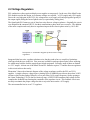
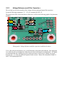
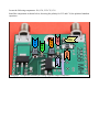
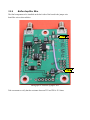
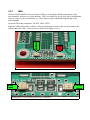
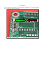
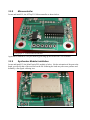
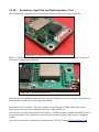
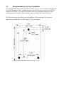
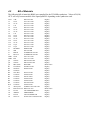
OpenSynth PLL
Construction Guide and User's Manual
Version 2.1
September , 2012
Tony Long – [email protected]
© Tony Long 2011
These materials are Open Source, licensed under
Creative Commons Attribution 3.0 Unported license.
See http://creativecommons.org/licenses/by/3.0 for details
Table of Contents
1. Basic Overview
1.1.
1.2.
1.3.
Basic Description / Features
Uses
Basic Block Diagram and Design Philosophy
2. How It Works
2.1.
Phase Locked Loop Synthesizer Basics
2.2.
Voltage Regulators
2.3.
Microcontroller and Code
2.3.1)
Microcontroller Hardware
2.3.2)
Synthesizer Programming Requirements
2.3.3)
Microcontroller Functional Code Description
2.3.4)
Microcontroller Programming Resources
3. How to Build it
← IF IMPATIENT, START HERE
3.1.
Introduction
3.2.
Step-by-Step Instructions
3.2.1)
RF Connector Installation
3.2.2)
Voltage Reference Filter Capacitors
3.2.3)
Voltage Regulator Components
3.2.4)
Buffer Amplifier Wire
3.2.5)
3.3V Regulator
3.2.6)
Buffer Amplifier
3.2.7)
LEDs
3.2.8)
Microcontroller
3.2.9)
Synthesizer Module Installation
3.2.10) Connectors, Heat Sink and Final Inspection / Test
3.3.
Recommendations for use/installation
4. Documentation
4.1.
4.2.
4.3.
Schematic Diagram
Bill of Materials
Microcontroller Code
1.1
Basic Description
The OpenSynth PLL kit you now have in front of you is a collection of parts needed to construct a low
phase noise, miniature frequency synthesizer. You probably already know this.
What you may not know is that the synthesizer features the following:
•
Miniature Size (1.5” by 2”)
•
Low Phase Noise*
•
Low DC Power Consumption*
•
Open Source Design
•
Extra I/O for Customization
•
Buffered Output
( * Specifications depend on synthesizer module used.)
1.2
Uses
This kit was designed to provide a local oscillator (LO) for amateur receivers and transmitters
operating at UHF and beyond. At the heart of the OpenSynth PLL is a phase locked loop (PLL)
module made by MiniCircuits (the large metal can part in the kit). These synthesizer modules are
available in a wide range of frequencies (~300 MHz to ~4 GHz in narrow bands) in the same physical
footprint and pinout. This affords great flexibility in the planning of multiplied-LO or multiple
conversion architectures while maintaining both low phase noise and power consumption.
Another feature of the OpenSynth PLL is the open nature of the design. All design files and source
code are freely available and may be used under the condition of attribution only. That is to say,
anyone can freely take the design and modify/reuse/repackage/resell it with the only condition that
attribution to Reactance Labs is stated.
Because the microcontroller code is open source and the microcontroller is very common in the
hobbyist community, modification to the code can be made to enable new features.
Other uses include (some require additional code and or hardware):
•
LO Source with switchable offset (useful for mixer-only millimeterwave radios where
the IF may not used during a CW transmission)
•
Beacon Transmitter With CW ID
•
Test Source
•
Frequency Hopped Source
•
Remotely Activated Transmitter
•
Narrow Band Swept Source
•
Microcontroller can be used for T/R sequencing or other uses in addition to PLL control
1.3
Basic Block Diagram and Design Philosophy
Illustration 1: Block Diagram of the OpenSynth PLL
The primary design goal for the OpenSynth kit was to develop a flexible circuit which would interface
with the wide variety of synthesizer modules presently manufactured by MiniCircuits for use as LO
sources for amateur microwave radios. The desire for several key characteristics led to the final design:
low phase noise, useful output power level, low power consumption, compact size, buildable by
experienced kit builders with basic tools, open design for expandability and
modification/customization.
With the exception of the output stage, all components have voltage regulators to maintain performance
under conditions of uncertain input power (such as when operating by battery power in a remote
location).
Most modern high performance RF components are surface mount and it is expected that most people
building a microwave radio have experience soldering tiny components. Certain SMT components
were excluded, however, specifically those that require reflow soldering techniques.
2.1
Phase Locked Loop Synthesizer Basics
The OpenSynth PLL kit incorporates a PLL frequency synthesizer. Since its initial introduction in the
1930's, the PLL controlled oscillator circuit has been gaining popularity. This increase in popularity
accelerated rapidly in the 1970's with the introduction of integrated circuit (IC) packaged PLL
solutions. Modern PLL ICs are smaller and operate at higher frequencies due to advanced
semiconductor and packaging technologies.
PLL synthesizers generally make excellent LOs for microwave radios as they can be extremely stable
in frequency and when properly designed, exhibit very low phase noise.
A PLL frequency synthesizer operates by comparing two independent oscillators and adjusting the
frequency and phase of one to match the other (the reference). The oscillator being adjusted is
commonly a Voltage Controlled Oscillator (VCO).
Illustration 2: Phase Locked Loop Frequency Synthesizer Diagram
In Illustration 2, the main blocks of a PLL synthesizer are shown. Synthesis begins with the startup of
the Reference Oscillator and VCO. Initially, these two may be running at slightly different frequencies
and certainly with different phase. The Phase Detector compares the two and generates a correction
signal which is amplified and then filtered by the Loop Filter, ultimately commanding the VCO to
move forward or backward in phase until the two oscillators are in sync. This condition is called
“phase lock” and is maintained as long as the drift of the VCO is within the “tracking range” of the
circuit.
A successful PLL synthesizer design results in a circuit that produces a spectrally pure signal (low
phase noise and low spurious signal levels) and locks up quickly and reliably (under varying
temperatures and component drift). The majority of the design work in modern integrated circuit
implementations is the design of the loop filter which usually takes the form of a low noise op-amp
filter circuit.
In high performance narrowband applications (such as required for amateur microwave transceivers), a
narrow band VCO is used. It is often the case that some oddball frequency is required when building a
radio, especially in multiple conversion architectures. The difficulty is that for each frequency, a new
PLL circuit must be designed. OpenSynth takes advantage of a large collection of designs done by
MiniCircuits to enable rapid construction of high quality signal sources.
These PLL modules are available in a wide range of frequency bands (with some gaps) from about 500
MHz to 4 GHz. Any of the synthesizers in the “DK1042 and DK801” package style will work with the
OpenSynth circuit board.
2.2 Voltage Regulators
PLL synthesizers often require multiple power supplies to run properly. In the case of the MiniCircuits
PLL modules used in this design, two separate voltages are required – a VCO supply and a PLL supply.
Due to the very high gain of the VCO, any voltage noise on its supply will end up magnified greatly in
the output signal, taking the form of phase noise (or equivalently, timing jitter).
The OpenSynth PLL features a pair of ultra-low noise discrete voltage regulators. Originally the circuit
was designed with common LM317s, but their contribution to phase noise was excessive. The addition
of the more complex and costly discrete regulators improved the close-in phase noise by 10-15 dB!
Illustration 3: Schematic diagram of the discrete voltage
regulators
Integrated ultra low noise regulator solutions exist, but they tend to have a couple key limitations
which preclude their use in this kit. First, most are available in packages that require reflow soldering,
for which many builders lack the required specialized equipment. Secondly, most of them are limited
to +5.5V output. At least one of the MiniCircuits PLL modules requires 7V and the discrete regulators
in this circuit achieve that easily.
Illustration 3 shows the schematic diagram of the voltage regulators used for the PLL and VCO
supplies. A single reference voltage source (Analog Devices ADR440) provides an ultra-clean 2.048V
reference which is then further filtered by a low pass filter (16 Hz corner frequency) before getting to
the Linear Technology LT1678 dual low noise op-amp. A 2N2222 NPN transistor and voltage divider
complete the feedback loop forming the remainder of the regulator circuit. This feedback circuit acts
not only to maintain the proper voltage but also to reject the noise on the +10V supply.
The microcontroller has its own 3.3V regulator.
2.3 Microcontroller and Code
The PLL chip within the MiniCircuits modules must be configured each time it is powered up.
OpenSynth PLL uses a microcontroller to send the appropriate commands to the PLL chip (any of
several Analog Devices PLL synthesizer chips).
As shipped, each microcontroller is pre-programmed to the frequency specified when ordering.
Provisions are made on the board for user reprogramming using any of several programmers including
the inexpensive AVRISP from Atmel. Source code is available on the Reactance Labs website as well
as in this document.
2.3.1
Microcontroller Hardware
The microcontroller used in this circuit is an 8-bit Atmel ATTiny2313. This microcontroller was
chosen for ease of programming (free C compilers exist and are well supported), its popularity in the
hobbyist community, and its large amount of I/O pins. It is an excessive microcontroller for the
application, but allows for additional applications which users may choose to implement.
Illustration 4: Microcontroller Pinout - Green blocks
indicate signal names
The ATTiny2313 has an internal oscillator and requires no external parts to function. As seen above in
Illustration 4, there are 18 total I/O pins, in banks called PB, PD, and PA. OpenSynth uses 4 pins to
communicate with the PLL module (LD (Lock Detect), CLK (Clock), DATA, and LE (Latch
Enable)).
LDO (Lock Detect Output) is an output line which lights an LED when the PLL is in a locked state. It
is tied to the 6-pin header connector as are PD3 – PD5 which are extra I/O pins available for
programming for other uses. PA0 is tied to a red LED on the PCB and is also user definable (as
delivered, this LED has no function).
2.3.2
Synthesizer Programming Requirements
Each MiniCircuits PLL module has a PLL controller chip which includes numerous functions requiring
configuration. In this section, the KSN-2534A-119+ module will be described. This unit uses an
Analog Devices ADF4153. The other modules use similar chips and require similar programming.
Four control registers require programming and are shown in Table 1.
The ADF4153 is a Fractional-N synthesizer, requiring the setting of an Integer divider (R0, DB22DB14), a Fractional divider (DB13-DB2), a 12-bit modulus (R1, DB13 -DB2). There is also a
reference divider (R1, DB17-DB14), a reference doubler (R2, DB11) and a bunch of other
miscellaneous registers that require setting.
1
1
1
MUXOUT
1
1
12-bit Fractional Value (FRAC)
0
1
0
0
0
0
0
0
0
0
1
0
DB7
DB6
DB5
DB4
DB3
DB2
DB1
DB0
0
1
1
1
0
0
0
0
0
56
4-bit R counter
12-bit Interpolator Modulus Value (MOD)
DB23 DB22 DB21 DB20 DB19 DB18 DB17 DB16 DB15 DB14 DB13 DB12 DB11 DB10 DB9
0
1
0
0
0
1
0
0
0
0
0
DB7
DB6
DB5
DB4
DB3
DB2
DB1
DB0
0
0
0
1
0
1
0
0
1
LDP
0
1
DB8
DB7
DB6
DB5
DB4
DB3
DB2
DB1
DB0
1
1
0
1
0
0
0
1
0
Control Bits
DB8
DB7
DB6
DB5
DB4
DB3
DB2
DB1
DB0
1
1
1
0
0
0
1
1
1
Noise And Spur Mode
DB10 DB9
0
Counter
Reset
0
Noise And
Spur Mode
0
CP ThreeState
0
Reserved
0
Control Bits
CP Current
Setting
DB15 DB14 DB13 DB12 DB11 DB10 DB9
0
PowerDown
R2
CP/2
Reference
Doubler
10
Resync
1
Control Bits
DB8
1
R3
Control Bits
DB8
250
Prescaler
0
Reserved
R1
0
Load
Control
R0
9-bit Integer Value (INT)
DB23 DB22 DB21 DB20 DB19 DB18 DB17 DB16 DB15 DB14 DB13 DB12 DB11 DB10 DB9
PD Polarity
Fast
Lock
In particular, the CP Polarity, and PD Polarity are set by the VCO and loop filter characteristics. These
values are supplied in the PLL module data sheets provided by MiniCircuits.
Reserved
Table 1: Programming Registers for ADF4153 to generate 2556 MHz
Fast Lock, Load Control, Prescalar, Resync, CP/2, LDP, Power-Down, CP Three-State, Counter Reset,
Control Bits and Reserved and the Noise and Spur Mode controls all should be left alone. The Counter
Reset is changed in the programming sequence described later. More details on all these functions can
be found in the data sheet of the PLL chip. The part number is indicated on each MiniCircuits PLL
module data sheet.
For the ADF4153, the following programming sequence is required:
1. Delay 100 msec (this is to let the voltage regulators stabilize)
2. Reset the Noise and Spur Register (R3) (send 0x000003)
3. Set Noise and Spur Register (R3) to nominal values (see table above)
4. Set Control Register with Counter set
5. Set R divider
6. Set N divider
7. Set Control Register with Counter reset
Values sent to the PLL module are in hex. To determine the hex value, convert the 24 bit binary values
above into a hex number.
To determine what values to program, and how to set the dividers, refer to the PLL IC data sheet. It
gives the required equations and examples to determine the proper values. Often there are multiple
solutions and in general it is preferred to keep the reference divider value as low as possible to maintain
good phase noise.
2.3.3
Microcontroller Functional Code Description
The OpenSynth code is straightforward. A function called transfer does most of the work in
actually generating the signals going to the PLL module. Specifically, the transfer function
generates clock pulses, data pulses, and sets and resets the Latch Enable which 'clocks in' data after
sending all of it. The remainder of the program simply calls transfer and supplies it with the
relevant data word and word length. This is done in accordance with the order of commands specified
in the PLL chip datasheets.
A final element of the code checks the status of the Lock Detect output of the PLL and lights the LED
when in lock.
2.3.4
Microcontroller Programming Resources
If you are new to programming microcontrollers, there are many great resources for learning about how
to program. Programming in the C language for microcontrollers is slightly different than for a
computer; bit-wise operations are used much more extensively for instance.
Also, to program a OpenSynth board you'll need an In circuit Serial Programmer (ISP) which can be
purchased at very reasonable prices from Atmel or other vendors.
Here are a few links to check out on programming Atmel microcontrollers:
Atmel's AVR series of microcontrollers:
http://www.atmel.com/products/AVR/
In-Circuit Serial Programming Tools:
http://www.atmel.com/dyn/products/tools_card.asp?tool_id=3808
http://www.adafruit.com/products/46
http://www.adafruit.com/products/26 (cheapest option, $7.50)
Comprehensive, basic introduction to programming AVRs:
http://hackaday.com/2010/10/23/avr-programming-introduction/
Bit Manipulation techniques: (The AVRfreaks.net forum is a great resource in general)
http://www.avrfreaks.net/index.php?name=PNphpBB2&file=viewtopic&t=37871
http://www.cprogramming.com/tutorial/bitwise_operators.html
http://www.avrfreaks.net/index.php?name=PNphpBB2&file=viewtopic&t=97219
3.1 Introduction
The OpenSynth PLL is not a beginner's kit, but should not present a challenge to experienced builders
of microwave electronics. With the exception of the connectors, all components are surface mount.
Several of the components are ESD sensitive, so take care to handle and build this kit in an ESD
controlled environment. A grounded (through a 1 Mohm resistor) ESD wrist strap and soldering iron
should be used at all times when handling and assembling parts or the finished kit. Many hobbyists
and engineers alike discount the significance of ESD, but to ensure that your synthesizer performs well
for a long time, it is important to follow good ESD practices.
Creating good solder joints is helped by using paste flux, and soaking up excess solder with solder
braid. It is crucial to clean flux from the board as it can cause performance problems in the long term.
The following tools are recommended for the assembly of the OpenSynth PLL kit.
•
ESD grounded temperature controlled soldering iron with fine tip
•
Fine gauge solder
•
Desoldering braid
•
Paste flux
•
A vise for holding the board
•
Magnifying glass / microscope
•
Diagonal wire cutter
•
Wire stripper
•
Hobby knife
•
Isopropyl alcohol
•
Cotton swabs
3.2 Step-by-Step Instructions
The OpenSynth PLL assembly is organized in a manner to allow incremental testing of circuit elements
before the next step of assembly. This assures that when they most sensitive components are placed,
they will not be damaged. It is recommended that assembly follow the steps below rather than all-atonce.
3.2.1
RF Connector Installation
Photograph 1: Various views of the SMA connectors used
on the OpenSynth board.
The two SMA connectors are the first parts to be installed. These connectors require some care to
install and solder. After carefully aligning the connectors to the board, (ensure that the center pins are
truly centered on their pads) solder just the center pins down. Next, solder the SMA connector ground
legs to the board. This step requires some patience and solder flux. Applying the flux prior to
soldering helps considerably in wetting the solder to the legs and the board. Additionally, it is
recommended that heat be applied to the legs themselves until solder flows on them, as they have a
higher thermal capacity than the thin metal of the circuit board. Take care to avoid using too much heat
(especially if using a hot air gun to preheat the joint) as the center contact can come loose and
alignment will be lost. Your solder joints should look like those in photographs 2 and 3 below.
Photograph 2: Example of good solder joints on the SMA connectors
Photograph 3: An example of good solder joints on the back side of
the PCB.
3.2.2
Voltage Reference and Filter Capacitors
The next step involves the assembly of the voltage reference and input/output filter capacitors.
Locate the following components: C1 – C5 (C4 is omitted), R1, R2, U3.
The bottom side of the circuit board has no silkscreen, so refer to the following graphics for placement
guidance:
C5
C9
C6
C7
U4
C2
C1
Photograph 4: Voltage Reference and filter capacitor installation locations
U4 is a fine pitch part and requires very careful attention to placement and soldering. One suggestion
is to solder two pins on a diagonal to anchor the part before soldering the remaining leads. It is highly
recommended that after soldering, the part be inspected under a microscope to identify any shorts
between pins. C1 is the only polarized capacitor in this section. Observe the orientation of both U4
and C1 in the photograph above.
Test Point 1
Once the precision voltage reference and input filter capacitors are installed as above, it is important to
test the output to make sure the circuit is working. Use the photograph below and probe at the indicated
test points in accordance with Table 2. Apply +12V at the +12V pin and record the values for TP1 and
+12V in the table for future reference.
TP1
+12V
GROUND
Photograph 5: Test points for the LDO regulator
Table 2: LDO Regulator Test Table
Label
Description
TP1
Vref Output (nominally +2.048V)
+12V
+12V Input
GROUND
Ground return
Measured Value
N/A
3.2.3
Voltage Regulator Components
This section describes the installation of the remaining components of the voltage regulator and filter
capacitors for the PLL and VCO supply lines.
Locate the following components: R4-R7, Q1, Q2, U5
R4 and R6 set the voltage for the PLL and VCO circuits respectively. There are 4 different voltages
required by the various MiniCircuits modules: 3.0, 3.3, 5, 7 V. Refer to Table 4 below for common
values, or if you need to change values for another module, refer to Table 5. Finally for any generic
voltage you can use Equation 1 to determine what value you need.
Table 4: Resistor values for commonly used Synthesizer Modules
MiniCircuits P/N
Frequency (typical)
PLL Voltage
VCO Voltage R4
KSN-1150A-119+
1152 MHz
5
5
215
215
KSN-2170A-219+
2160 MHz
5
5
215
215
KSN-2534A-119+
2556 MHz
3
5
69.8
215
KSN-3500A-119+
3312 MHz
3
7
69.8
360
Table 5: Resistor values for all four possible voltages
Voltage (PLL or VCO)
Resistor Value (R4 or R6)
3
69.8
3.3
91
5
215
7
360
Equation 1: Equation to
determine resistor values
R6
Refer to the following photograph for component positions.
Q1
C4
Q1
C4
C8
C8*
R4
R4
R5
R5
Q2
Q2
R6
R6
U
U5
5
R7
R7
Photograph 6: Location of regulator components (* Note, C8 is rotated in current PCB)
Locate the following components: R9, C10, C12-C15, C18
Install the components as shown below, observing the polarity for C12 and C14, the polarized tantalum
capacitors.
C15
R9
C10
C14
C13
C12
C18
Photograph 7: Component locations for voltage regulator output components
Test Point 3
Once all the components are installed as above, it is important to test the outputs to make sure the
circuit is working. Use the photograph below and probe at the indicated test points in accordance with
Table 2. Record the values for TP3, TP4, and +12V in the table for future reference. TP3 is the PLL
supply voltage and TP4 is the VCO supply voltage. Each are measured on the positive terminal of the
black tantalum capacitors shown below. Apply +12V as in the previous two sections.
TP3
TP4
Photograph 8: Voltage Regulator Components Installed
Table 6:
Voltage Regulator Test Table
Label
Description
TP3
PLL Supply Voltage (see Table 4 or 5
for which voltage to expect)
TP4
VCO Supply Voltage (see Table 4 or 5
for which voltage to expect)
+12V
+12V Input
Measured Value
3.2.4
Buffer Amplifier Wire
The final components to be installed on the back side of the board is the jumper wire
Install the wire as shown below:
TP5
TP6
Photograph 9: Location of jumper wire
Take a moment to verify that the resistance between TP5 and TP6 is 215 ohms.
3.2.5
3.3V Regulator
The microcontroller runs off 3.3V and requires a regulator. These components are to be installed onto
the top side of the board. Locate and install C11 and U6 as below.
TP7
U6
Ground
+12V
Photograph 10: Installation of the 3.3V regulator and filter capacitor
Test Point 4
Once the 3.3V regulator and filter capacitor are installed as above, it is important to test the output to
make sure the circuit is working. Use the photograph below and probe at the indicated test points in
accordance with Table 7. Apply +12V at the +12V pin and record the values for TP7 and +12V in the
table for future reference.
Table 7: LDO Regulator Test Table
Label
Description
TP7
Regulator Output (nominally +3.3V)
Pin 20 of U1
+12V
+12V Input
GROUND
Ground return
Measured Value
3.2.6
Buffer Amplifier
In addition to providing extra output power, the buffer amplifier isolates the output of the PLL from
whatever load may be attached to the OpenSynth PLL board.
Locate the following components: C26, C17, Q3, ATT1*
Install the components as in the photograph below. Take care to note the orientation of Q3 as well as
ATT1. If ATT1 is not installed properly as shown, the output power will be substantially lower than
expected.
* - Each kit is supplied with a range of values for ATT1. See Table 8 below for suggested
values.
Photograph 11: Installation of the buffer amplifier components
Table 8: Attenuator value suggestions
MiniCircuits P/N
Frequency (typical)
Attenuator Value (dB)
KSN-1150A-119+
1152 MHz
4
KSN-2170A-219+
2160 MHz
4
KSN-2534A-119+
2556 MHz
4
KSN-3500A-119+
3312 MHz
7
Take a moment to verify there are no shorts in the circuit by applying +12V as in the previous step and
monitor the DC current to make sure that it does not exceed 100 mA (should be well below this).
3.2.7
LEDs
Of the two LEDs installed, only one of them (LED1) is used with the default programming of the
microcontroller, and serves as a lock indicator. LED2 is available for use by users who want additional
status or even as a power on indicator, etc. These features require additional programming of the
microcontroller.
Locate the following components: R8, R10, LED1, LED2
Install the LEDs and resistors as shown. Take special attention to observe the tiny green stripe at the
cathode end of the LEDs. You may have to tilt the LED slightly to see it.
RED
GREEN
Photograph 12: LED and resistor placement
Green
Stripe
Photograph 13: Close-Up detail of the LED orientation
Green
Stripe
Test Point 5
The LEDs should be tested with the +12V disconnected. Instead, apply 3.3V to the pads indicated
below to observe the function of each LED.
LED 1 (GREEN)
Photograph 14: LED Testing points
LED 2 (RED)
3.2.8
Microcontroller
Locate and install U1, the ATTiny2313 Microcontroller as shown below.
Photograph 15: Installed microcontroller
Again take a moment to verify no shorts by powering up the circuit with +12V as before.
3.2.9
Synthesizer Module Installation
Locate and install U2, the MiniCircuits PLL module as below. Not the orientation of the part to the
board, specifically that of the text label on the lid. Soldering the leads may take some patience and
definitely a fine tipped soldering iron.
Photograph 16: PLL Module Installed
3.2.10
Connectors, Heat Sink, and Final Inspection / Test
The last parts to be assembled are the programming header and the power/control connector.
Photograph 17: Connectors Installed
Finally, if you have not already done so, solder each end of the PLL Synthesizer lid to the circuit board.
This ensure a good ground connection.
Photograph 18: Lid soldered to board
The last step is the installation of the heat sink. Remove the adhesive tape cover from the heat sink and
stick onto the top of the silver PLL synthesizer module
Construction is now complete! Take a few minutes to carefully inspect all the solder joints, spaces
between pins, and remove any remaining solder flux, solder splatter, etc.
After you have carefully inspected the board, connect a 10 MHz reference (0 dBm) to the REF port and
measure the output of your synthesizer on your favorite spectrum analyzer, power meter, or frequency
counter.
If you have any questions, comments, or need assistance, feel free to email [email protected]
3.3
Recommendations for Use/ Installation
Your OpenSynth PLL board can be mounted in a number of ways. First is by using #4 standoffs and
screws and mounting to a plate. Another method is to mount the board on a panel using the SMA
connectors for support. If you choose this method, make sure to install the connectors as in the
assembly guide, to avoid stress-induced damage when securing the nuts on the connectors.
The following drawing should help guide the installation of the OpenSynth PLL in whatever
application you intend. Holes are 0.125 inch (3.175 mm) in diameter.
Illustration 5: Hole Pattern for the OpenSynth PLL
4.0
Documentation
4.1
Schematic Diagram
4.2
Bill of Materials
The following bill of materials (BOM) was compiled for the 2556 MHz synthesizer. Values of R4, R6,
ATT1 will vary between models of the OpenSynth PLL depending on the synthesizer used.
ATT1
C1
C2
C3
C5
C6
C7
C9
C11
C12
C13
C14
C15
C16
C17
J1
J2
J3
J4
LED1
LED2
Q1
Q2
Q3
R1
R2
R3
R4
R5
R6
R7
R8
R9
R10
U1
U2
U3
U4
U5
U6
7 dB
10 uF
0.1 uF
1 uF
10 uF
0.1 uF
0.1 uF
1 uF
10 uF
10 uF
0.1 uF
10 uF
0.1 uF
15 pF
15 pF
HEADER
6PH
REF IN
RF OUT
Green
Red
2N2222
2N2222
ERA-2SM+
4.87k ohms
680 ohms
10k ohms
69.8 ohms
150 ohms
215 ohms
150 ohms
120 ohms
215 ohms
150 ohms
ATTiny2313
KSN-2534-119+
LT1762
ADR440
LT1678
NCP1117
PAT127CT-ND
718-1760-1-ND
478-1423-1-ND
587-1291-1-ND
490-5523-1-ND
478-1423-1-ND
478-1423-1-ND
478-6247-1-ND
490-5523-1-ND
718-1760-1-ND
478-1423-1-ND
718-1760-1-ND
478-1423-1-ND
478-6576-1-ND
478-6576-1-ND
WM4204-ND
609-3202-ND
CONSMA003.062-ND
CONSMA003.062-ND
160-1169-1-ND
160-1167-1-ND
PZT2222ACT-ND
PZT2222ACT-ND
ERA-2SM+
P4.87KCCT-ND
P680ACT-ND
P69.8CCT-ND
P150ACT-ND
P215CCT-ND
P150ACT-ND
P120ACT-ND
P215AACT-ND
P150ACT-ND
ATTINY2313V-10SU-ND
KSN-2534-119+
LT1762EMS8#PBF-ND
ADR440ARMZ
LT1678CS8#PBF-ND
NCP1117ST33T3GOSCT-ND
Digikey
Digikey
Digikey
Digikey
Digikey
Digikey
Digikey
Digikey
Digikey
Digikey
Digikey
Digikey
Digikey
Digikey
Digikey
Digikey
Digikey
Digikey
Digikey
Digikey
Digikey
Digikey
Digikey
MiniCircuits
Digikey
Digikey
Digikey
Digikey
Digikey
Digikey
Digikey
Digikey
Digikey
Digikey
Digikey
MiniCircuits
Digikey
Digikey
Digikey
Digikey
4.3
Microcontroller Source Code
This code was written for the 2556 MHz model.
/*
* MiniSynth_KSN-2534_2556.c
*
* Created: 12/17/2011 12:56:08 PM
* Author: Tony Long KC6QHP
*/
#include <avr/io.h>
#include <util/delay.h>
#define CLK PB2 /* Clock output line to synthesizer module */
#define DATA PB1
/* Data output line to synthesizer module */
#define LE PB0
/* Latch enable */
#define LD PB3
/* Lock detect INPUT from synthesizer module */
#define LDO PD2 /* Lock detect OUTPUT pin (to LED anode and 'lock' pad on PCB) */
void transfer(uint32_t nData, uint8_t nNumBits)
{
uint8_t j; /* initialize the j variable used in the loop */
PORTB &= ~(1<<LE); /* Set LE low */
PORTB &= ~(1<<CLK); /* Set CLK low */
_delay_us(50);
/* Delay for LE setup time, > 20 nsec */
for(j=0; j<nNumBits; j++) {
if (nData & ((uint32_t)1<<(nNumBits-1-j)))
PORTB |= 1<<DATA; /* set DATA output pin to high */
else
PORTB &= ~(1<<DATA); /* set DATA output to low */
_delay_us(20);
PORTB |= (1<<CLK); /* Set CLK high (This is the clock pulse that clocks in data)*/
_delay_us(20);
PORTB &= ~(1<<CLK); /* Set CLK low (This is the end of the pulse) */
_delay_us(20);
}
PORTB |= 1<<LE; /* set LE high */
_delay_us(100); /*Delay for LE hold time */
PORTB &= ~(1<<LE); /* Set LE low */
_delay_us(50);
}
int main(void)
{
DDRB |= (1<<PB0)|(1<<PB1)|(1<<PB2); /* set outputs PB0=CLK, PB1=DATA, PB2=LE */
DDRB &= ~(1<<PB3); /*set LD pin to input */
DDRD |= (1<<PD2); /* set output PD2=LDO */
/* THIS IS THE VARIABLE DECLARATION SECTION */
uint32_t Nreg; /* initialize the N Divider Register as a 32 bit integer */
uint32_t Rreg; /* initialize the R Divider Register as a 32 bit integer */
uint32_t Creg; /* initialize the Control Register as a 32 bit integer */
uint32_t NSreg; /* initialize the Noise and Spur Register as a 32 bit integer */
/* THIS IS THE USER DATA SECTION */
Nreg = 0x3FC060; /* set nominal value of Nreg */
Rreg = 0x1440A1; /* set nominal value of Rreg */
Creg = 0x0001E2; /* set nominal value of Creg */
NSreg = 0x0003C7; /* set nominal value of NSreg */
/* THIS IS THE PROGRAM */
_delay_ms(100); /* Give the PLL a chance to boot up or whatever */
transfer(0x000003, 11); /* Reset the Noise and Spur Register */
transfer(NSreg, 11); /* Set the Noise and Spur Register to nominal values */
Creg |= ((uint32_t)1<<(uint32_t)3); /* Enable the Counter Register by writing 1 to DB2 */
transfer(Creg, 16); /* Transfer the Control Register values with the enabled counter */
transfer(Rreg, 24); /* Load the R divider register values */
transfer(Nreg, 24); /* Load the N divider register values */
Creg &= ~((uint32_t)1<<(uint32_t)3); /* Reset the Counter Register by writing 0 to DB2 */
transfer(Creg, 16); /* Reload the Control Register with the Counter disabled */
while(1) {
DDRD |= (1<<LDO);
if ( PINB & (1<<LD))
PORTD |= (1<<LDO);
else
PORTD &= ~(1<<LDO);
}
return 0;
}