1
Channel Isolated Analog-Digital Converter Module
Channel Isolated Analog-Digital Converter Module
(With Signal Conditioning Function)
User's Manual
-Q68AD-G
-Q66AD-DG
-GX Configurator-AD (SW2D5C-QADU-E)
SAFETY PRECAUTIONS
(Read these precautions before using this product.)
Before using this product, please read this manual and the relevant manuals carefully and pay full attention
to safety to handle the product correctly.
In this manual, the safety precautions are classified into two levels: "
WARNING" and "
CAUTION".
WARNING
Indicates that incorrect handling may cause hazardous conditions,
resulting in death or severe injury.
CAUTION
Indicates that incorrect handling may cause hazardous conditions,
resulting in minor or moderate injury or property damage.
Under some circumstances, failure to observe the precautions given under "
CAUTION" may lead to
serious consequences.
Observe the precautions of both levels because they are important for personal and system safety.
Make sure that the end users read this manual and then keep the manual in a safe place for future
reference.
[Design Precaution]
WARNING
Do not write data into the "system area" of the buffer memory of intelligent function modules. Also,
do not use any "prohibited to use" signals as an output signal to an intelligent function module
from the programmable controller CPU.
Writing data into the "system area" or outputting a signal for "prohibited to use" may cause a
malfunction of the programmable controller system.
CAUTION
Do not bunch the control wires or communication cables with the main circuit or power wires, or
install them close to each other.
They should be installed 100mm(3.9inch) or more from each other.
Not doing so could result in noise that may cause malfunction.
A-1
[Installation Precautions]
CAUTION
Use the programmable controller in an environment that meets the general specifications
contained in the user's manual of the CPU module to use.
Using this programmable controller in an environment outside the range of the general
specifications may cause electric shock, fire, malfunction, and damage to or deterioration of the
product.
While pressing the installation lever located at the bottom of module, insert the module fixing tab
into the fixing hole in the base unit until it stops. Then, securely mount the module with the fixing
hole as a supporting point.
For the Q66AD-DG, secure the module with fixing brackets after installation to the base unit.
When using the Q68AD-G in an environment where they are frequent vibrations, screw the module
to the base unit after installation.
Tighten the screws within the range of specified torque.
If the screws are loose, it may cause the module to fallout, short circuits, or malfunction.
If the screws are tightened too much, it may cause damage to the screw and/or the module,
resulting in fallout, short circuits or malfunction.
Be sure to shut off all phases of the external power supply used by the system before mounting or
removing the module.
Not doing so may cause damage to the module.
In the system where a CPU module supporting the online module change is used and on the
MELSECNET/H remote I/O stations, modules can be replaced online (during energizing).
However, there are some restrictions on replaceable modules and the replacement procedures
are predetermined for each module.
For details, refer to the chapter of the online module change in this manual.
Do not directly touch the conductive area or electronic components of the module.
Doing so may cause malfunction or failure in the module.
A-2
[Wiring Precautions]
CAUTION
Always ground the FG terminal.
Not doing so can cause an electric shock or malfunction.
When turning on the power and operating the module after wiring is completed, always attach the
terminal cover that comes with the product.
There is a risk of electric shock if the terminal cover is not attached.
Tighten the terminal screws within the range of specified torque.
If the terminal screws are loose, it may result in short circuits or malfunction.
If the terminal screws are tightened too much, it may cause damage to the screw and/or the
module, resulting in short circuits or malfunction.
Be careful not to let foreign matter such as sawdust or wire chips get inside the module.
They may cause fires, failure or malfunction.
The top surface of the module is covered with protective film to prevent foreign objects such as
cable offcuts from entering the module when wiring.
Do not remove this film until the wiring is complete.
Before operating the system, be sure to remove the film to provide adequate ventilation.
A-3
[Starting and Maintenance Precautions]
CAUTION
Do not disassemble or modify the modules.
Doing so could cause failure, malfunction injury or fire.
Be sure to shut off all phases of the external power supply used by the system before mounting or
removing the module.
Not doing so may cause failure or malfunction of the module.
In the system where a CPU module supporting the online module change is used and on the
MELSECNET/H remote I/O stations, modules can be replaced online (during energizing).
However, there are some restrictions on replaceable modules and the replacement procedures
are predetermined for each module.
For details, refer to the chapter of the online module change in this manual.
Do not install/remove the module to/from the base unit more than 50 times after the first use of the
product. (IEC 61131-2 compliant)
Failure to do so may cause malfunction.
Do not touch the connector while the power is on.
Doing so may cause malfunction.
Be sure to shut off all phases of the external power supply before cleaning or retightening the
terminal screws or module fixing screws.
Not doing so may cause failure or malfunction of the module.
If the screws are loose, it may cause the module to fallout, short circuits, or malfunction.
If the screws are tightened too much, it may cause damages to the screws and/or the module,
resulting in the module falling out, short circuits or malfunction.
Always make sure to touch the grounded metal to discharge the electricity charged in the body,
etc., before touching the module.
Failure to do so may cause a failure or malfunctions of the module.
[Disposal Precautions]
CAUTION
When disposing of this product, treat it as industrial waste.
A-4
CONDITIONS OF USE FOR THE PRODUCT
(1) Mitsubishi programmable controller ("the PRODUCT") shall be used in conditions;
i) where any problem, fault or failure occurring in the PRODUCT, if any, shall not lead to any major
or serious accident; and
ii) where the backup and fail-safe function are systematically or automatically provided outside of
the PRODUCT for the case of any problem, fault or failure occurring in the PRODUCT.
(2) The PRODUCT has been designed and manufactured for the purpose of being used in general
industries.
MITSUBISHI SHALL HAVE NO RESPONSIBILITY OR LIABILITY (INCLUDING, BUT NOT
LIMITED TO ANY AND ALL RESPONSIBILITY OR LIABILITY BASED ON CONTRACT,
WARRANTY, TORT, PRODUCT LIABILITY) FOR ANY INJURY OR DEATH TO PERSONS OR
LOSS OR DAMAGE TO PROPERTY CAUSED BY the PRODUCT THAT ARE OPERATED OR
USED IN APPLICATION NOT INTENDED OR EXCLUDED BY INSTRUCTIONS, PRECAUTIONS,
OR WARNING CONTAINED IN MITSUBISHI'S USER, INSTRUCTION AND/OR SAFETY
MANUALS, TECHNICAL BULLETINS AND GUIDELINES FOR the PRODUCT.
("Prohibited Application")
Prohibited Applications include, but not limited to, the use of the PRODUCT in;
• Nuclear Power Plants and any other power plants operated by Power companies, and/or any
other cases in which the public could be affected if any problem or fault occurs in the PRODUCT.
• Railway companies or Public service purposes, and/or any other cases in which establishment of
a special quality assurance system is required by the Purchaser or End User.
• Aircraft or Aerospace, Medical applications, Train equipment, transport equipment such as
Elevator and Escalator, Incineration and Fuel devices, Vehicles, Manned transportation,
Equipment for Recreation and Amusement, and Safety devices, handling of Nuclear or
Hazardous Materials or Chemicals, Mining and Drilling, and/or other applications where there is a
significant risk of injury to the public or property.
Notwithstanding the above, restrictions Mitsubishi may in its sole discretion, authorize use of the
PRODUCT in one or more of the Prohibited Applications, provided that the usage of the PRODUCT
is limited only for the specific applications agreed to by Mitsubishi and provided further that no
special quality assurance or fail-safe, redundant or other safety features which exceed the general
specifications of the PRODUCTs are required. For details, please contact the Mitsubishi
representative in your region.
A-5
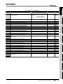
REVISIONS
* The manual number is given on the bottom left of the back cover.
Print Date
*Manual Number
Oct., 2006
SH (NA)-080647ENG-A
First edition
Revision
Jan., 2007
SH(NA)-080647ENG-B
Correction
Section 3.3.2, 3.4.12, 4.6.2, 6.3.1, 6.3.2, 6.5.1, 6.5.2
Jan., 2008
SH(NA)-080647ENG-C
Correction
SAFETY PRECAUTIONS, About the Generic Terms and Abbreviations, Section
1.1, Section 2.1, Section 2.3, Section 3.2.1, Section 3.4.1, Section 4.1, Section
4.4.2, Section 4.6.1, Section 4.6.2, Section 5.2.1, Section 5.2.2, Section 5.3.2,
Section 5.3.3, Section 5.6.1, Section 5.6.4, Section 5.6.5, Section 7.3.3, Section
7.3.5, Section 8.1, Appendix 1, Appendix 1.1, Appendix 1.2, Appendix 1.3
Addition
Section 2.2
May, 2008
SH(NA)-080647ENG-D
Correction
SAFETY PRECAUTIONS, Compliance with the EMC and Low Voltage Directives, About the Generic Terms and Abbreviations, Section 2.1, 2.3, Section
3.1.1, 3.2.1, 3.2.4, Section 4.1, 4.3, Section 5.2.1, 5.2.2, 5.3.1, 5.3.2, 5.3.3,
Chapter 7, Section 7.1
Oct., 2008
SH(NA)-080647ENG-E
Correction
Section 2.1, Section 3.1.1, 3.1.2, 3.2, 3.2.1, 3.2.3, 3.2.6, 3.3.2, 3.4.1, 3.4.2,
3.4.4, 3.4.7, 3.4.9, 3.4.11, 3.4.12, 3.4.13, 3.4.22, Section 4.3, 4.5, Section 5.1,
5.4, Section 8.1, 8.2.4, 8.2.6, Appendix 1.1, 1.2, 1.3
Addition
Appendix 2
Sep., 2011
SH(NA)-080647ENG-F
Correction
SAFETY PRECAUTIONS, COMPLIANCE WITH THE EMC AND LOW VOLTAGE DIRECTIVES, Section 4.6.1, 4.6.2, 4.6.3, 6.2.1, 6.2.2, 6.2.3, 6.3, 6.3.1,
6.3.2, 6.4, 6.4.1, 6.4.2, 6.4.3, 6.5, 6.5.1, 6.5.2
Addition
CONDITIONS OF USE FOR THE PRODUCT
Feb., 2012
SH(NA)-080647ENG-G
Correction
SAFETY PRECAUTIONS, COMPLIANCE WITH THE EMC AND LOW VOLTAGE DIRECTIVES, Section 1.1, 2.1 to 2.3, 3.1.1, 3.1.2, 3.2, 3.2.1, 3.2.3, 3.2.4,
3.2.6, 3.3.2, 3.4.1, 3.4.2, 3.4.4, 3.4.5, 3.4.7, 3.4.10, 3.4.15 to 3.4.17, 3.4.19,
3.4.21, 3.4.22, 3.4.25, 4.1, 4.1.1, 4.3, 4.4.2, 4.5, 4.6.1, 4.6.2, 5.2.1, 5.2.2, 5.3.1,
5.3.3, 5.4, 5.5, 5.6.1 to 5.6.3, 6.2.1, 6.2.2, 6.3, 6.3.1, 6.4.1, 6.4.2, 6.5, 6.5.1,
Chapter 7, 7.1, 7.2, 7.3.1 to 7.3.6, 7.5, 8.1, 8.2.4, 8.2.6, Appendix 2, Appendix 3
Japanese Manual Version SH-080645-I
This manual confers no industrial property rights or any rights of any other kind, nor does it confer any patent
licenses. Mitsubishi Electric Corporation cannot be held responsible for any problems involving industrial
property rights which may occur as a result of using the contents noted in this manual.
© 2006 MITSUBISHI ELECTRIC CORPORATION
A-6
INTRODUCTION
Thank you for purchasing the MELSEC-Q series programmable controller.
Before using the equipment, please read this manual carefully to develop full familiarity with the functions
and performance of the Q series programmable controller you have purchased, so as to ensure
correct use.
Please forward a copy of this manual to the end user.
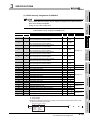
CONTENTS
SAFETY PRECAUTIONS .................................................................................................................................A - 1
CONDITIONS OF USE FOR THE PRODUCT..................................................................................................A - 5
REVISIONS.......................................................................................................................................................A - 6
INTRODUCTION...............................................................................................................................................A - 7
CONTENTS ......................................................................................................................................................A - 7
MANUALS.......................................................................................................................................................A - 11
COMPLIANCE WITH THE EMC, LOW VOLTAGE, AND MACHINERY DIRECTIVES .................................. A - 11
GENERIC TERMS AND ABBREVIATIONS....................................................................................................A - 12
PACKING LIST ............................................................................................................................................... A - 12
1 OVERVIEW
1.1
1 - 1 to 1 - 3
Features........................................................................................................................................... 1 - 1
2 SYSTEM CONFIGURATION
2 - 1 to 2 - 8
2.1
Applicable Systems ......................................................................................................................... 2 - 1
2.2
Precautions on System Configuration ............................................................................................. 2 - 5
2.3
How to Check the Function Version, Serial No., and Software Version .......................................... 2 - 6
3 SPECIFICATIONS
3.1
Performance Specifications ............................................................................................................. 3 - 1
3.1.1
3.1.2
3.1.3
3.2
A/D conversion methods ...................................................................................................... 3 - 15
Maximum and minimum values hold function....................................................................... 3 - 18
Input signal error detection function ..................................................................................... 3 - 18
Warning output function........................................................................................................ 3 - 25
Conversion starting time setting function (Q66AD-DG only) ................................................ 3 - 29
Scaling Function ................................................................................................................... 3 - 30
I/O Signals for the Programmable Controller CPU ........................................................................ 3 - 33
3.3.1
3.3.2
3.4
Performance specifications list ............................................................................................... 3 - 1
I/O conversion characteristic .................................................................................................. 3 - 5
Accuracy............................................................................................................................... 3 - 12
Function List .................................................................................................................................. 3 - 13
3.2.1
3.2.2
3.2.3
3.2.4
3.2.5
3.2.6
3.3
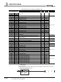
3 - 1 to 3 - 74
List of I/O signals .................................................................................................................. 3 - 33
Details of I/O signals............................................................................................................. 3 - 35
Buffer Memory ............................................................................................................................... 3 - 42
3.4.1
Buffer memory assignment................................................................................................... 3 - 42
A-7
3.4.2
3.4.3
3.4.4
3.4.5
3.4.6
3.4.7
3.4.8
3.4.9
3.4.10
3.4.11
3.4.12
3.4.13
3.4.14
3.4.15
3.4.16
3.4.17
3.4.18
3.4.19
3.4.20
3.4.21
3.4.22
3.4.23
3.4.24
3.4.25
A/D conversion enable/disable setting (Un\G0).................................................................... 3 - 54
CH[ ] average time/average number of times/moving average/time constant settings
(Un\G1 to Un\G8) ................................................................................................................. 3 - 55
A/D conversion completed flag (Un\G10) ............................................................................. 3 - 56
CH[ ] digital output value (Un\G11 to Un\G18) ..................................................................... 3 - 57
Write data error code (Un\G19) ............................................................................................ 3 - 58
Setting range (Un\G20, Un\G21) .......................................................................................... 3 - 58
Offset/gain setting mode offset/gain specification (Un\G22, Un\G23) .................................. 3 - 59
Averaging process specification (Un\G24, Un\G25))............................................................ 3 - 60
CH[ ] maximum value/minimum value storage area (Un\G30 to Un\G45)............................ 3 - 61
Input signal error detection extended/input signal error detection setting(Un\G47).............. 3 - 61
Warning output settings (Un\G48) ........................................................................................ 3 - 63
Input signal error detection flag (Un\G49) ............................................................................ 3 - 64
Warning output flag (Un\G50,Un\51) .................................................................................... 3 - 65
Scaling enable/disable setting (Un\G53) .............................................................................. 3 - 65
CH[ ] scaling value storage area (Un\G54 to Un\G61) ......................................................... 3 - 66
CH[ ] scaling upper / lower limit value (Un\G62 to Un\G77) ................................................. 3 - 66
CH[ ] conversion starting time setting (for 2-wire transmitter) (Un\G78 to Un\G83)
(Q66AD-DG only) ................................................................................................................. 3 - 66
CH[ ] process alarm upper/lower limit value (Un\G86 to Un\G117) ...................................... 3 - 67
CH[ ] rate alarm warning detection period (Un\G118 to Un\G125) ....................................... 3 - 68
CH[ ] rate alarm upper/lower limit value (Un\G126 to Un\G141) .......................................... 3 - 69
CH[ ] input signal error detection setting value/CH[ ] Input signal error detection lower limit setting
value (Un\G142 to Un\G149)
CH[ ] Input signal error detection upper limit setting value (Un\G150 to Un\G157) .............. 3 - 70
Mode switching setting (Un\G158, Un\G159) ....................................................................... 3 - 73
Save data classification setting (Un\G200) (Q68AD-G only) ................................................ 3 - 73
Factory default and User range settings offset/gain value (Un\G202 to Un\G233) .............. 3 - 74
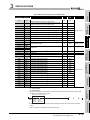
4 SETUP AND PROCEDURES BEFORE OPERATION
4.1
4 - 1 to 4 - 22
Handling Precautions....................................................................................................................... 4 - 1
4.1.1
Attaching a module fixing bracket (Q66AD-DG only) ............................................................. 4 - 2
4.2
Setup and Procedures before Operation ......................................................................................... 4 - 3
4.3
Part Names ...................................................................................................................................... 4 - 4
4.4
Wiring............................................................................................................................................... 4 - 7
4.4.1
4.4.2
Wiring precautions .................................................................................................................. 4 - 7
External wiring ........................................................................................................................ 4 - 8
4.5
Intelligent Function Module Switch Setting .................................................................................... 4 - 10
4.6
Offset/Gain Settings....................................................................................................................... 4 - 12
4.6.1
4.6.2
4.6.3
Offset/gain settings (Q68AD-G)............................................................................................ 4 - 13
Offset/gain settings (Q66AD-DG) ......................................................................................... 4 - 17
A/D conversion value storage during offset/gain setting ...................................................... 4 - 22
5 UTILITY PACKAGE (GX Configurator-AD)
5 - 1 to 5 - 33
5.1
Utility Package Functions ................................................................................................................ 5 - 1
5.2
Installing and Uninstalling the Utility Package ................................................................................. 5 - 2
5.2.1
A-8
Handling precautions .............................................................................................................. 5 - 2
5.2.2
5.3
Operating environment ........................................................................................................... 5 - 4
Utility Package Operation ................................................................................................................ 5 - 6
5.3.1
5.3.2
5.3.3
Common utility package operations ....................................................................................... 5 - 6
Operation overview................................................................................................................. 5 - 9
Starting the intelligent function module utility ....................................................................... 5 - 11
5.4
Initial Setting .................................................................................................................................. 5 - 14
5.5
Auto Refresh Setting...................................................................................................................... 5 - 16
5.6
Monitoring/Test .............................................................................................................................. 5 - 18
5.6.1
5.6.2
5.6.3
5.6.4
5.6.5
Monitor/test screen ............................................................................................................... 5 - 18
Offset/gain setting operation................................................................................................. 5 - 21
Confirmation of conversion characteristic............................................................................. 5 - 23
Pass data (Q68AD-G) .......................................................................................................... 5 - 25
Pass data (Q66AD-DG)........................................................................................................ 5 - 27
5.7
FB Conversion of Initial Setting/Auto Refresh Setting ................................................................... 5 - 28
5.8
Usage of FB................................................................................................................................... 5 - 30
5.8.1
5.8.2
5.8.3
Outline .................................................................................................................................. 5 - 30
Paste an FB to a sequence program.................................................................................... 5 - 32
Convert (compile) a sequence program ............................................................................... 5 - 33
6 PROGRAMMING
6 - 1 to 6 - 38
6.1
Programming Procedure.................................................................................................................. 6 - 1
6.2
For Use in Normal System Configuration (Q68AD-G) ..................................................................... 6 - 2
6.2.1
6.2.2
6.2.3
6.3
For Use in Remote I/O Network (Q68AD-G) ................................................................................. 6 - 11
6.3.1
6.3.2
6.4
Programming example using the utility package .................................................................. 6 - 14
Programming example without using the utility package...................................................... 6 - 17
For Use in Normal System Configuration (Q66AD-DG) ................................................................ 6 - 21
6.4.1
6.4.2
6.4.3
6.5
Before creating a program...................................................................................................... 6 - 3
Programming example using the utility package .................................................................... 6 - 5
Programming example without using the utility package........................................................ 6 - 8
Before creating a program.................................................................................................... 6 - 22
Programming example using the utility package .................................................................. 6 - 24
Programming example without using the utility package...................................................... 6 - 27
For Use in Remote I/O Network (Q66AD-DG)............................................................................... 6 - 30
6.5.1
6.5.2
Programming example using the utility package .................................................................. 6 - 32
Programming example without using the utility package...................................................... 6 - 35
7 ONLINE MODULE CHANGE
7 - 1 to 7 - 38
7.1
Online Module Change Conditions .................................................................................................. 7 - 2
7.2
Online Module Change Operations ................................................................................................. 7 - 3
7.3
Online Module Change Procedure .................................................................................................. 7 - 4
7.3.1
7.3.2
When industrial shipment setting is used and initial setting was made with
GX Configurator-AD ............................................................................................................... 7 - 5
When industrial shipment setting is used and initial setting was made with
sequence program................................................................................................................ 7 - 10
A-9
7.3.3
7.3.4
7.3.5
7.3.6
When user range setting is used and initial setting was made with GX Configurator-AD
(other system is available) .................................................................................................... 7 - 15
When user range setting is used and initial setting was made with GX Configurator-AD
(other system is unavailable) ................................................................................................ 7 - 20
When user range setting is used and initial setting was made with sequence program
(other system is available) .................................................................................................... 7 - 26
When user range setting is used and initial setting was made with sequence program
(other system is unavailable) ................................................................................................ 7 - 31
7.4
Range Reference Table................................................................................................................. 7 - 37
7.5
Precautions for Online Module Change ......................................................................................... 7 - 38
8 TROUBLESHOOTING
8 - 1 to 8 - 8
8.1
Error Code List................................................................................................................................ 8 - 1
8.2
Troubleshooting ............................................................................................................................... 8 - 5
8.2.1
8.2.2
8.2.3
8.2.4
8.2.5
8.2.6
APPENDIX
When the "RUN" LED is flashing or turned off........................................................................ 8 - 5
When the "ERR." LED is on or flashing .................................................................................. 8 - 5
When the "ALM" LED is on or flashing ................................................................................... 8 - 5
When the digital output values cannot be read ...................................................................... 8 - 6
When A/D conversion completed flag does not turn ON during use in normal mode............. 8 - 7
Checking the A/D converter module status using GX Developer system monitor ................. 8 - 7
App - 1 to App - 15
Appendix 1 Dedicated Instruction List and Available Devices..................................................................App- 1
Appendix 1.1G(P).OFFGAN .................................................................................................................App- 2
Appendix 1.2G(P).OGLOAD .................................................................................................................App- 4
Appendix 1.3G(P).OGSTOR.................................................................................................................App- 8
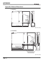
Appendix 2 Functions Added or Changed Due to Version Upgrade ......................................................App- 13
Appendix 3 External Dimensions............................................................................................................App- 15
INDEX
A - 10
Index - 1 Index - 2
MANUALS
The manuals related to this product are listed below.
Please place an order as needed.
Relevant Manuals
Manual number
Manual name
(model code)
GX Developer Version 8 Operating Manual
Operating methods of GX Developer, such as programming, printing, monitoring, and debugging
(Sold separately)
GX Developer Version 8 Operating Manual (Function Block)
Operating methods of GX Developer, such as creating and printing function blocks
(13JU41)
SH-080376E
(Sold separately)
GX Works2 Version1 Operating Manual (Common)
System configuration, parameter settings, and online operations (common to Simple project and Structured
project) of GX Works2
SH-080373E
(Sold separately)
(13JU44)
SH-080779ENG
(13JU63)
Remark
Printed manuals are available separately. Please place an order with the manual
number (model code) in the table above.
COMPLIANCE WITH THE EMC, LOW VOLTAGE, AND MACHINERY DIRECTIVES
(1) Method of ensuring compliance
To ensure that Mitsubishi programmable controllers maintain EMC and Low Voltage
Directives when incorporated into other machinery or equipment, certain measures
may be necessary. Please refer to one of the following manuals.
• MELSEC-L CPU Module User's Manual (Hardware Design, Maintenance and
Inspection)
• MELSEC-L CC-Link IE Field Network Head Module User's Manual
• Safety Guidelines
(This manual is included with the CPU module or head module.)
The CE mark on the side of the programmable controller indicates compliance with
EMC and Low Voltage Directives.
(2) Additional measures
No additional measures are necessary for the compliance of this product with EMC
and Low Voltage Directives.
A - 11
GENERIC TERMS AND ABBREVIATIONS
Unless otherwise specified, this manual uses the following general terms and
abbreviations.
General term/Abbreviation
Description
A/D converter module
A generic term for the Q68AD-G and Q66AD-DG
DOS/V personal computer
An IBM PC/AT
GX Developer
GX Works2
GX Configurator-AD
or compatible computer with DOS/V
The product name of the software package for the MLSEC programmable controllers
The abbreviation for the analog-digital converter module setting and monitor tool GX Configurator-AD (SW2D5C-QADU-E)
A generic term for the Q00JCPU, Q00CPU, Q01CPU, Q02CPU, Q02HCPU, Q06HCPU, Q12HCPU,
Q25HCPU, Q02PHCPU, Q06PHCPU, Q12PHCPU, Q25PHCPU, Q12PRHCPU, Q25PRHCPU,
QCPU (Q mode)
Q00UJCPU, Q00UCPU, Q01UCPU, Q02UCPU, Q03UDCPU, Q04UDHCPU, Q06UDHCPU,
Q10UDHCPU, Q13UDHCPU, Q20UDHCPU, Q26UDHCPU, Q03UDECPU, Q04UDEHCPU,
Q06UDEHCPU, Q10UDEHCPU, Q13UDEHCPU, Q20UDEHCPU, Q26UDEHCPU, Q50UDEHCPU,
and Q100UDEHCPU
Process CPU
A generic term for the Q02PHCPU, Q06PHCPU, Q12PHCPU and Q25PHCPU
Redundant CPU
Generic term for Q12PRHCPU and Q25PRHCPU.
Personal computer
A generic term for DOS/V personal computers
Industrial shipment setting
FB
A generic term for analog input ranges 0 to 10V, 0 to 5V, 1 to 5V, -10 to 10V, 0 to 20mA, and 4 to
20mA
The abbreviation for function block
A generic term for the following:
Windows Vista
Microsoft Windows Vista
Home Basic Operating System,
Microsoft Windows Vista
Home Premium Operating System,
Microsoft Windows Vista
Business Operating System,
Microsoft Windows Vista
Ultimate Operating System,
Microsoft Windows Vista
Enterprise Operating System
A generic term for the following:
Windows XP
Microsoft Windows XP Professional Operating System,
Microsoft Windows XP Home Edition Operating System
A generic term for the following:
Microsoft Windows 7 Starter Operating System,
Microsoft Windows 7 Home Premium Operating System,
Microsoft Windows 7 Professional Operating System,
Windows 7
Microsoft Windows 7 Ultimate Operating System,
Microsoft Windows 7 Enterprise Operating System
Note that the 32-bit version is designated as "32-bit Windows 7", and the 64-bit version is designated as "64-bit Windows 7".
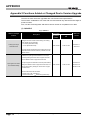
PACKING LIST
The product package contains the following.
Model
Q68AD-G
A - 12
Product
Type Q68AD-G Channel Isolated Analog-Digital Converter Module
Quantity
1
Model
Product
Type Q66AD-DG Channel Isolated Analog-Digital Converter Module (with Signal
Q66AD-DG
SW2D5C-QADU-E
SW2D5C-QADU-EA
Conditioning Function)
Quantity
1
FG terminal L-Shaped metal fitting
1
GX Configurator-AD Version 2 (1-license product)(CD-ROM)
1
GX Configurator-AD Version 2 (Multiple-license product)(CD-ROM)
1
A - 13
1
1
OVERVIEW
OVERVIEW
This User's Manual describes the specifications, handling and programming methods for
the type Q68AD-G channel isolated analog-digital converter module (hereinafter referred
to as the Q68AD-G) and type Q66AD-DG channel isolated analog-digital converter
module (with signal conditioning function) (hereinafter referred to as the Q66AD-DG),
which are used with the MELSEC-Q series CPU modules.
The Q66AD-DG is exclusively used for current input.
In this manual, the Q68AD-G and Q66AD-DG are collectively referred to as the A/D
converter modules.
1.1
Features
(1) Channel isolated
The channels are isolated.
The Q66AD-DG is also isolated between the external supply power and channels.
(2) Multi-channel analog input is available.
(a) By using a single Q68AD-G, analog voltage or current inputs of 8 points
(8 channels) are available.
(b) A single Q66AD-DG allows connection of 2-wire transmitters of 6 points
(6 channels).
It has an input range for analog current, in addition to connections to 2-wire
transmitters.
(3) Power supply to 2-wire transmitter (Q66AD-DG only)
Supplying power to the 2-wire transmitter, the Q66AD-DG does not require the power
supply for the 2-wire transmitter.
Supply power can be switched ON/OFF channel-by-channel by the A/D conversion
enable/disable setting.
(4) Module protection provided by short-circuit protection circuit
(Q66AD-DG only)
If an excessive current flows into the module due to a short circuit of the wiring, the
short-circuit protection circuit limits the current to within 25 to 35mA, protecting the
module.
(5) Analog input check by check terminals (Q66AD-DG only)
Measurement of a voltage at the check terminals allows the mA of the 2-wire
transmitter output to be checked without the wiring being disconnected.
1-1
1.1 Features
OVERVIEW
1
The reference accuracy *1 is as high as ±0.1% and the temperature coefficient*2 is as high
as ±71.4ppm/°C.
*1 Accuracy of offset/gain setting at ambient temperature
OVERVIEW
(6) High accuracy
2
*2 Accuracy per temperature change of 1°C
The input range*3 can easily be set from the GX Developer.
*3 Input range refers to the type of offset/gain settings. The most frequently used range is set as the
default but the user can also set the offset/gain.
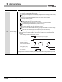
(8) A/D conversion system*1
There are the following five A/D conversion systems.
(a) Sampling processing
Analog input values are converted into digital values one by one on a channel
basis and the digital output value is output at every conversion.
(b) Averaging processing
1) Time averaging
A/D conversion is averaged in terms of time on a channel basis and a digital
average value is output.
2) Count averaging
A/D conversion is averaged in terms of count on a channel basis and a digital
average value is output.
3) Move averaging
The specified number of digital output values measured per sampling time are
averaged.
4
5
6
PROGRAMMING
(c) Primary delay filter
A digital output value is smoothed according to the preset time constant.
3
SPECIFICATIONS
(7) Changing the input range
SETUP AND
PROCEDURES
BEFORE OPERATION
5°C
(temperature variation difference) = 0.1357%
UTILITY PACKAGE
(GX CONFIGURATORAD)
0.1% (reference accuracy) + 0.00714 %/°C (temperature coefficient)
SYSTEM
CONFIGURATION
Example) Accuracy when the temperature varies from 25 to 30°C
*1 Refer to Section 3.2.1 for the details of the A/D conversion system.
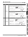
(9) Input signal error detection function
7
The voltage/current outside the setting range is detected.
ONLINE MODULE
CHANGE
(10)Warning output*1
There are the following two warning outputs.
(a) Process alarm
A warning is output if a digital output value falls outside the setting range.
(b) Rate alarm
A warning is output if the varying rate of a digital output value falls outside the
preset varying rate range.
*1 Refer to Section 3.2.4 for details on warning output.
1.1 Features
1-2
8
TROUBLESHOOTING
1
1
OVERVIEW
(11)Scaling function
A/D conversion values can be converted to percentage values (%) in the preset range
and be loaded into the buffer memory. This function can reduce the time required for
programming. (Refer to Section 3.2.6.)
(12)Online module change
Furthermore, the following operations can be processed by using sequence programs. (Note that these operations are possible for the modules of the same model
only.) (Refer to Chapter7.)
• Transferring the offset/gain set values to the replacement A/D converter module
• Transferring the offset/and gain set values to another A/D converter module
mounted on the other slot
(13)Offset/gain setting
GX Configurator-AD, dedicated instruction (G(P).OFFGAN) or mode switching setting
allows a shift to the offset/gain setting mode easily.
(14)Easy settings using GX Configurator-AD
Using GX Configurator-AD which is sold separately, sequence programs can be
reduced since settings of the A/D converter module can be made on the screen.
Also, the set status or operating status of the module can be checked easily.
A FB*1 can be created automatically from the set intelligent function module parameter, and can be used in sequence programs.
*1 FB is the function for making a circuit block used in a sequence program repeatedly a part (FB) to
use it in the sequence program.
This function can improve the efficiency of program development and minimize program bugs to
improve program qualities.
For the details of FB, refer to "GX Developer Version 8 Operating Manual (Function
Block)."
1-3
1.1 Features
2
SYSTEM CONFIGURATION
1
OVERVIEW
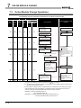
SYSTEM CONFIGURATION
This chapter explains the system configuration of the A/D converter module.
Applicable Systems
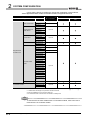
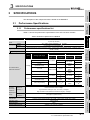
(1) Applicable modules and base units, and No. of modules
(a) When mounted with a CPU module
The table below shows the CPU modules and base units applicable to the A/D
converter module and quantities for each CPU model.
Depending on the combination with other modules or the number of mounted
modules, power supply capacity may be insufficient.
Pay attention to the power supply capacity before mounting modules, and if the
3
SPECIFICATIONS
This section describes the applicable systems.
SYSTEM
CONFIGURATION
2
SETUP AND
PROCEDURES
BEFORE OPERATION
4
UTILITY PACKAGE
(GX CONFIGURATORAD)
5
PROGRAMMING
6
7
ONLINE MODULE
CHANGE
2.1
8
TROUBLESHOOTING
2
2.1 Applicable Systems
2-1
2
SYSTEM CONFIGURATION
power supply capacity is insufficient, change the combination of the modules.
Table2.1 Applicable modules, number of mountable modules, and applicable base units
Base unit*2
Applicable CPU module
CPU type
CPU model
Q00JCPU
Basic model QCPU
Q00CPU
Q01CPU
No. of modules*1
Main base unit
Extension base
unit
Up to 16
Up to 24
Q02CPU
High Performance
model QCPU
Q02HCPU
Q06HCPU
Up to 64
Q12HCPU
Q25HCPU
Q02PHCPU
Process CPU
Q06PHCPU
Q12PHCPU
Up to 64
Q25PHCPU
Redundant CPU
Q12PRHCPU
Q25PRHCPU
Q00UJCPU
Q00UCPU
Q01UCPU
Programmable
Q02UCPU
controller CPU
Q03UDCPU
Up to 53
Up to 16
Up to 24
Up to 36
Q04UDHCPU
Q06UDHCPU
Q10UDHCPU
Q13UDHCPU
Universal model
QCPU
Q20UDHCPU
Q26UDHCPU
Q03UDECPU
Q04UDEHCPU
Up to 64
Q06UDEHCPU
Q10UDEHCPU
Q13UDEHCPU
Q20UDEHCPU
Q26UDEHCPU
Q50UDEHCPU
Q100UDEHCP
U
Safety CPU
QS001CPU
N/A
Q06CCPU-V
C Controller module
Q06CCPU-V-B
Up to 64
Q12DCCPU-V
: Applicable,
: N/A
*1 Limited within the range of I/O points for the CPU module.
*2 Can be installed to any I/O slot of a base unit.
*3 An extension base unit cannot be connected to a safety CPU.
Remark
To use the A/D converter module with a C Controller module, refer to the user's
manual for the C Controller module.
2-2
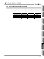
2.1 Applicable Systems
SYSTEM CONFIGURATION
No. of modules
*2
Base unit
*1
Main base unit of
Extension base unit
remote I/O station
of remote I/O station
QJ72LP25-25
: Applicable,
: N/A
*1 Limited within the range of I/O points for the network module.
*2 Can be installed to any I/O slot of a base unit.
SPECIFICATIONS
QJ72BR15
Remark
The Basic model QCPU or C Controller module cannot create the MELSECNET/
H remote I/O network.
(2) Support of the multiple CPU system
When using the A/D converter in a multiple CPU system, refer to the following manual
first.
• QCPU User's Manual (Multiple CPU System)
(a) Applicable A/D converter module
The A/D converter module is of the function version C from the first product, and
applicable to a multiple CPU system.
(b) Intelligent function module parameters
Write intelligent function module parameters to only the control CPU of the A/D
converter module.
(3) Compatibility with online module change
The A/D converter module is of the function version C from the first product, and
online module change is possible.
For the procedure of online module change, refer to Chapter7.
SETUP AND
PROCEDURES
BEFORE OPERATION
4
5
UTILITY PACKAGE
(GX CONFIGURATORAD)
QJ72LP25GE
3
Up to 64
6
PROGRAMMING
QJ72LP25G
7
ONLINE MODULE
CHANGE
Applicable network module
2
SYSTEM
CONFIGURATION
(b) Mounting to a MELSECNET/H remote I/O station
The table below shows the network modules and base units applicable to the A/D
converter module and quantities for each network module model.
Depending on the combination with other modules or the number of mounted
modules, power supply capacity may be insufficient.
Pay attention to the power supply capacity before mounting modules, and if the
power supply capacity is insufficient, change the combination of the modules.
OVERVIEW
1
8
TROUBLESHOOTING
2
2.1 Applicable Systems
2-3
2
SYSTEM CONFIGURATION
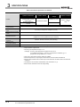
(4) Supported software packages
Relation between the system containing the Q68AD-G and software package is
shown in the following table.
GX Developer or GX Works2 is required to use the A/D converter module.
Software Version
GX Developer
Q00J/Q00/Q01CPU
Single CPU system
Version 7 or later
Multiple CPU system
Version 8 or later
Q02/Q02H/Q06H/
Single CPU system
Version 4 or later
Q12H/Q25HCPU
Multiple CPU system
Version 6 or later
Q02PH/Q06PHCPU
Q12PH/Q25PHCPU
Q12PRH/
Single CPU system
Multiple CPU system
Single CPU system
Multiple CPU system
Redundant CPU system
Q25PRHCPU
Q00UJ/Q00U/
Single CPU system
Q01UCPU
Multiple CPU system
Q02U/Q03UD/
Single CPU system
Q04UDH/
Multiple CPU system
Q06UDHCPU
Q10UDH/
Single CPU system
Q20UDHCPU
Multiple CPU system
Q13UDH/
Single CPU system
Q26UDHCPU
Multiple CPU system
Q03UDE/Q04UDEH/
Single CPU system
Q06UDEH/Q13UDEH/
Q26UDEHCPU
Multiple CPU system
Q10UDEH/
Single CPU system
Q20UDEHCPU
Multiple CPU system
Q50UDEH/
Single CPU system
Q100UDEHCPU
Multiple CPU system
If installed in a MELSECNET/H remote I/O station
GX Configurator-AD
GX Works2
Version 1.10N or later
Version 1.08J or later
Version 8.68W or later
Cannot be used
Version 7.10L or later
Version 8.45X or later
Version 8.76E or later
Version 2.09K or later
Version 8.48A or later
Version 8.76E or later
Version 1.08J or later
Version 8.62Q or later
Version 8.68W or later
Version 8.76E or later
Cannot be used
Cannot be used
Version 1.13H or later
Version 6 or later
Version 2.09K or later
Cannot be used
Depending on the version of GX Configurator-AD, applicable system, CPU
module and functions of A/D converter module.
Refer to Appendix 2 for details.
2-4
2.1 Applicable Systems
2
SYSTEM CONFIGURATION
1
OVERVIEW
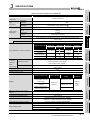
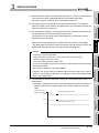
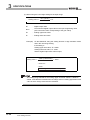
Precautions on System Configuration
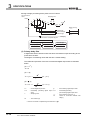
(1) When using the A/D converter module with Redundant CPU
(a) Dedicated instruction
The dedicated instruction cannnot be used.
(b) GX Configurator-AD connection
GX Configurator-AD cannot be used when accessing Redundant CPU via an
intelligent function module on an extension base unit from GX Developer.
Connect a personal computer with a communication path indicated below.
SYSTEM
CONFIGURATION
2
3
2
SPECIFICATIONS
1
Main base unit
SETUP AND
PROCEDURES
BEFORE OPERATION
4
Extension base unit
5
1
Direct connection to use the CPU
2
Connection through an intelligent function module on the main base unit
(Through Ethernet module, MELSECNET/H module, or CC-Link module)
UTILITY PACKAGE
(GX CONFIGURATORAD)
(GX Configurator-AD cannot be used.)
PROGRAMMING
6
ONLINE MODULE
CHANGE
7
8
TROUBLESHOOTING
2.2
2.2 Precautions on System Configuration
2-5
2
SYSTEM CONFIGURATION
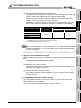
2.3
How to Check the Function Version, Serial No., and Software
Version
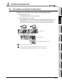
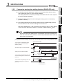
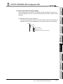
(1) Checking the function version and serial No.
The serial No. and function version of the A/D converter module can be checked on
the rating plate, front of the module, and system monitor of GX developer.
(a) On the rating plate
The rating plate is put on the side of the A/D converter module.
Serial No. (Upper 5 digits)
Function version
-C
Relevant regulation
standards
(b) On the front of the module
The function version and serial No. on the rating plate is also indicated on the
front of the module (lower part)
Function version
Serial No.
2-6
2.3 How to Check the Function Version, Serial No., and Software Version
SYSTEM CONFIGURATION
1
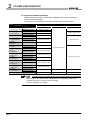
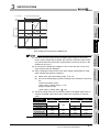
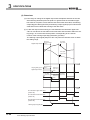
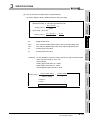
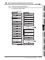
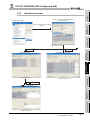
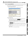
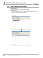
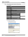
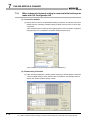
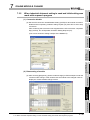
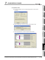
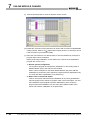
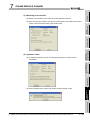
(c) On the system monitor (product information list)
tor]
[System moni-
OVERVIEW
To display the system monitor, select [Diagnostics]
Product Inf. List of GX Developer.
Function
version
2
Product
No.
SYSTEM
CONFIGURATION
Serial
No.
SETUP AND
PROCEDURES
BEFORE OPERATION
The serial No. on the rating plate and the front of the module may be different from
the serial No. displayed on the product information list in GX Developer.
• The serial No. on the rating plate and the front of the module indicates the
management information of the product.
• The serial No. displayed on the product information list in GX Developer
indicates the function information of the product. The function information
of the product is updated when a new function is added.
4
5
UTILITY PACKAGE
(GX CONFIGURATORAD)
1) Production number
Production number indication is not available for the A/D converter module; "-"
is shown.
SPECIFICATIONS
3
PROGRAMMING
6
ONLINE MODULE
CHANGE
7
8
TROUBLESHOOTING
2
2.3 How to Check the Function Version, Serial No., and Software Version
2-7
2
SYSTEM CONFIGURATION
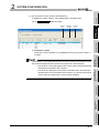
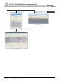
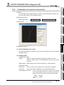
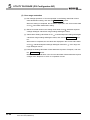
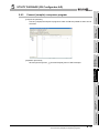
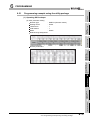
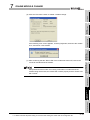
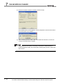
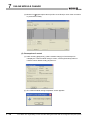
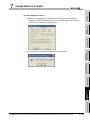
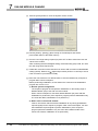
(2) Checking the software version of GX Configurator-AD
The software version of GX Configurator-AD can be checked on GX Developer by
clicking [Help]
[Product information].
Software version
(In the case of GX Developer Version 8)
2-8
2.3 How to Check the Function Version, Serial No., and Software Version
3
SPECIFICATIONS
1
OVERVIEW
SPECIFICATIONS
The description of this chapter and later is based on the Q68AD-G.
2
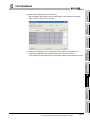
Performance specifications list
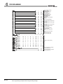
Table 3.1 shows the performance specifications of the A/D converter modules.
Item
Specifications
Number of analog input
8 points (8 channels)
points
Analog input
Voltage
-10 to 10VDC (Input impedance 1 M
Current
or more)
0 to 20mADC (Input resistance 250 )
16-bit signed binary (normal resolution mode: –4096 to 4095, high resolution mode: –12288 to 12287,
Digital output
–16384 to 16383)
Using scaling function
16-bit signed binary (-32768 to 32767)
Normal resolution mode
Input
Analog input range
Maximum
Digital
Maximum
output value
resolution
output value
resolution
2.5 mV
0 to 16000
0 to 4000
1.25 mV
0 to 10V
0 to 5V
1 to 5V
1 to 5V
Voltage
I/O characteristics,
maximum resolution
(Extended mode)
1.0 mV
-1000 to 4500
1.0 mV
-10 to 10V
*7
2.5 mV
-4000 to 4000
0.375 m V*8
Users range setting
0 to 20mA
4 to 20mA
Current
4 to 20mA
(Extended mode)
Users range setting
High resolution mode
Digital
0 to 4000
-1000 to 4500
-4000 to 4000
5
A
4
A
4
A
1.37
A*8
0.625 mV
0.416 mV
0 to 12000
0.333 mV
-3000 to
0.333 mV
13500
-16000 to
0.625 mV
16000
-12000 to
12000
0.333 mV*8
0 to 12000
-3000 to
13500
-12000 to
12000
1.66
A
1.33
A
1.33
A
1.33
A*8
±0.1%
relative to
digital output
value)
accuracy
*1
*2
High resolution mode (Other than the above ranges) : ±12digit*2
Temperature
coefficient *3
Common mode
characteristic
Response time
±71.4ppm/°C (0.00714%/°C)
Common mode voltage, Input-Common ground (input voltage 0V): 500VAC
Common mode voltage rejection ratio (VCM < 500V): 60Hz 107dB, 50Hz 106dB
Sampling cycle*4
*5
Absolute maximum input
6
7
Normal resolution mode : ±4digit*2
High resolution mode (0 to 10V, -10 to 10V) : ±16digit
5
ONLINE MODULE
CHANGE
(Accuracy
Reference
4
8
10ms/ channel
TROUBLESHOOTING
Accuracy
SPECIFICATIONS
3
Table3.1 Performance Specifications of Q68AD-G
SETUP AND
PROCEDURES
BEFORE OPERATION
3.1.1
SYSTEM
CONFIGURATION
Performance Specifications
UTILITY PACKAGE
(GX CONFIGURATORAD)
3.1
PROGRAMMING
3
20ms
Voltage: ± 15V Current: ± 30mA*6
3.1 Performance Specifications
3.1.1 Performance specifications list
3-1
3
SPECIFICATIONS
Table3.1 Performance Specifications of Q68AD-G
Item
Specifications
Specific isolated area
Isolation method
Dielectric withstand
voltage
Insulation resistance
Between input terminal and
Isolation
programmable controller
500VAC rms, 1min.
power supply
Transformer isolation
Between analog input
or
more
1000VAC rms, 1min.
channels
Maximum number of writes
Up to 50,000 times
to flash memory
Number of I/O occupied
16 points (I/O assignment: Intelligent 16 points)
points
External wiring connection
40-pin connector
system
Applicable wire size
500VDC, 10M
0.3mm2(AWG22) or less (for A6CON1, A6CON4)
0.088mm2 to 0.24mm2(AWG28 to 24) (for A6CON2)
External device connection
A6CON1, A6CON2, A6CON4 (sold separately)
connector
Internal current
0.46A
consumption (5VDC)
Weight
0.16kg
*1 Accuracy of offset/gain setting at ambient temperature
*2 "digit" indicates a digital value.
*3 Accuracy per temperature change of 1°C
Example) Accuracy when temperature changes from 25 to 30°C
0.1% (reference accuracy) + 0.00714 %/°C (temperature coefficient)
5°C
(temperature change difference) = 0.1357%
*4 The cycle in which A/D conversion values are updated.
*5 The time required for an input signal to reach the A/D converter inside the Q68AD-G.
*6 Current value indicates value of instant input current that does not break module inner electrical
resistance.
*7 For details on I/O conversion characteristics, refer to Section3.1.2 (1).
*8 The maximum resolution for the user range setting
3-2
3.1 Performance Specifications
3.1.1 Performance specifications list
3
SPECIFICATIONS
1
Table3.2 Performance Specifications of Q66AD-DG
Specifications
6 points (6 channels)
transmitters)
With 2-wire
transmitter
specification
Without 2-wire
4 to 20mADC (Input resistance 250 )
transmitter
Supply voltage
26±2VDC
Maximum supply
Supply power
current
specification
Short-circuit
24mADC
Available
protection
Limit current: 25 to 35mA
3
Available
Check terminals
16-bit signed binary (-32768 to 32767)
Normal resolution mode
Analog input range
I/O characteristics, maximum resolution*8
Maximum
Digital out-
Maximum
put value
resolution
put value
resolution
0 to 20mA
0 to 4000
4 to 20mA
4 to 20mA
-1000 to 4500
(Extended mode)
Users range setting*4
Accuracy
A
4
A
4
0 to 4000
1.37
0 to 12000
-3000 to
A
A*9
13500
0 to 12000
1.66
A
1.33
A
1.33
A
1.33
A*9
±0.1%
Reference accuracy
(Normal resolution mode: ±4digit *2
*1
*3
output value) Temperature coefficient
±71.4ppm/°C (0.00714 %/°C)
Sampling cycle*5
10ms/ channel
time*6
20ms
±30mA*7
Absolute maximum output
Specific isolated area
Isolation method
Dielectric withstand
Insulation
voltage
resistance
programmable controller
Between analog input
channels
500VAC rms, 1min.
isolation
Between external supply
Number of I/O occupied points
External wiring connection system
Applicable wire size
External device connection connector
or
more
7
Up to 50,000 times
16 points (I/O assignment: Intelligent 16 points)
40-pin connector
0.3mm2(AWG22) or less (for A6CON1, A6CON4)
0.088mm2 to 0.24mm2(AWG28 to 24) (for A6CON2)
8
A6CON1, A6CON2, A6CON4 (sold separately)
TROUBLESHOOTING
memory
1000VAC rms, 1min.
10M
500VAC rms, 1min.
power and analog input
Maximum number of writes to flash
500VDC
Transformer
ONLINE MODULE
CHANGE
power supply
24VDC +20%, -15%
External supply power
Ripple, spike within 500mVP-P
Inrush current : 5.0A, within 400µs
0.36A
3.1 Performance Specifications
3.1.1 Performance specifications list
6
PROGRAMMING
Between I/O terminal and
Isolation
4
5
High resolution mode: ±12digit *2)
digital
Response
5
UTILITY PACKAGE
(GX CONFIGURATORAD)
relative to
High resolution mode
Digital out-
SETUP AND
PROCEDURES
BEFORE OPERATION
–288 to 12287)
Using scaling function
SPECIFICATIONS
16-bit signed binary (normal resolution mode: –96 to 4095, high resolution mode:
Digital output
(Accuracy
2
0 to 20mADC±1 (Input resistance 250 )
SYSTEM
CONFIGURATION
Input
OVERVIEW
Item
Number of analog input points (2-wire
3-3
3
SPECIFICATIONS
Table3.2 Performance Specifications of Q66AD-DG
Item
Specifications
Internal current consumption (5VDC)
0.42A
Weight
0.22kg
*1 Accuracy of offset/gain setting at ambient temperature
Q66AD-DG needs to be powered on 30 minutes prior to operation for compliance to the
specification (accuracy).
*2 "digit" indicates a digital value.
*3 Accuracy per temperature change of 1°C
Example) Accuracy when temperature changes from 25 to 30°C
0.1% (reference accuracy) + 0.00714 %/°C (temperature coefficient)
5°C
(temperature change difference) = 0.1357%
*4 User range setting is 2 to 24mA
*5 The cycle in which A/D conversion values are updated.
*6 The time required for an input signal to reach the A/D converter inside the Q66AD-DG.
*7 Current value indicates value of instant input current that does not break module inner electrical
resistance.
*8 For details on I/O conversion characteristics, refer to Section3.1.2 (2).
*9 The maximum resolution for the user range setting
Remark
See the user's manual for the CPU module being used for general specifications
of the A/D converter modules.
3-4
3.1 Performance Specifications
3.1.1 Performance specifications list
SPECIFICATIONS
1
The offset value denotes the analog input value (voltage or current) that makes the digital
output value 0.
Gain value
The gain value denotes the analog input value (voltage or current) that makes the digital
output value:
4000 (in normal resolution mode)
16000/12000 (in high resolution mode)
SYSTEM
CONFIGURATION
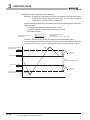
Offset value
2
3
SPECIFICATIONS
The I/O conversion characteristic represents the angle formed by a straight line
connecting the "offset value" and "gain value" when the analog signals (voltage or current
input) from outside the programmable controller are converted to digital values.
OVERVIEW
I/O conversion characteristic
SETUP AND
PROCEDURES
BEFORE OPERATION
4
UTILITY PACKAGE
(GX CONFIGURATORAD)
5
PROGRAMMING
6
7
ONLINE MODULE
CHANGE
3.1.2
8
TROUBLESHOOTING
3
3.1 Performance Specifications
3.1.2 I/O conversion characteristic
3-5
3
SPECIFICATIONS
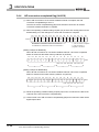
(1) Input characteristics of Q68AD-G
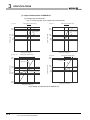
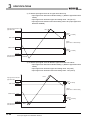
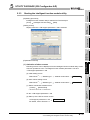
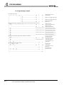
(a) Voltage input characteristic
Fig. 3.1 shows a graph of the voltage input characteristic.
Analog input practical range
1) 1 to 5V
Analog input practical range
2) 0 to 5V
High resolution mode
High resolution mode
12287
12000
12287
12000
4095
4000
0
0
-96
-288
Normal resolution
mode
Digital output value
Digital output value
Normal resolution
mode
01
4095
4000
5
0
Analog input voltage (V)
16383
16000
High resolution mode
4095
4000
0
0
Normal resolution mode
-4000
-4096
-10
0
Digital output value
High resolution mode
Digital output value
Analog input practical range
4) 0 to 10V
16383
16000
-16000
-16384
4095
4000
0
-96
-384
10
Analog input voltage (V)
Fig.3.1 Voltage input characteristic of Q68AD-G (1/2)
3-6
5
Analog input voltage (V)
Analog input practical range
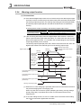
3) -10 to 10V
0
0
-96
-288
3.1 Performance Specifications
3.1.2 I/O conversion characteristic
0
Normal resolution mode
0
Analog input voltage (V)
10
3
SPECIFICATIONS
1
OVERVIEW
Analog input practical range
3) -10 to 10V
16383
16000
High resolution mode
0
0
SYSTEM
CONFIGURATION
4095
4000
Normal resolution mode
-4000
-4096
0
10
Analog input voltage (V)
Fig.3.1 Voltage input characteristic of Q68AD-G (2/2)
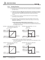
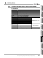
(a) Offset value, gain value setting range: 10 to 10V
(b) Use one of the following formulas according to the resolution mode to be
set.
1) Normal resolution mode
{ (Gain value) - (Offset value) } > 1.5V
2) High resolution mode
{ (Gain value) - (Offset value) } 4.0V
(4) When an analog value that exceeds the range for the digital output value is
entered, the digital output value will be fixed at the maximum or minimum
value.
Analog input
range setting
1 to 5V
0 to 5V
Normal resolution mode
Minimum
-96
-10 to 10V
-4096
0 to 10V
-96
1 to 5V
(Extended mode)
User range setting
Maximum
4095
High resolution mode
Minimum
Maximum
-288
12287
-16384
-384
16383
-1096
4595
-3288
13787
-4096
4095
-12288
12287
3.1 Performance Specifications
3.1.2 I/O conversion characteristic
3-7
5
UTILITY PACKAGE
(GX CONFIGURATORAD)
(1) Set within the analog input range and digital output range for each input
range. If these ranges are exceeded, the maximum resolution and accuracy
may not fall within the performance specifications. (Avoid use shown by the
dotted lines in Fig.3.1.)
(2) Do not input an analog input voltage of -15V or less and 15V or more The
input elements may be damaged.
(3) Set the offset/gain values for the User range setting marked within a range
which satisfies the following conditions.
SETUP AND
PROCEDURES
BEFORE OPERATION
4
6
PROGRAMMING
-10
7
ONLINE MODULE
CHANGE
-16000
-16384
SPECIFICATIONS
3
8
TROUBLESHOOTING
Digital output value
2
3
SPECIFICATIONS
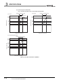
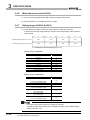
(b) Current input characteristic
Fig. 3.2 shows a graph of the current input characteristic
1) 4 to 20mA
Practical analog input range
Analog input practical range
2) 0 to 20mA
High resolution
mode
High resolution mode
12287
12000
Normal resolution
mode
4095
4000
0
-96
-288
0
0 4
Digital output value
Digital output value
12287
12000
Normal resolution
mode
4095
4000
0
0
-96
-288
20
Analog input current (mA)
0
3) 4 to 20mA (Expanded mode)
Analog input practical range
High resolution
mode
13787
13500
12000
Digital output value
Normal resolution
mode
4595
4500
4000
0
-1000
-1096
-3000
-3288
0
0 4
20 22
Analog input current (mA)
Fig.3.2 Current input characteristic of Q68AD-G
3-8
3.1 Performance Specifications
3.1.2 I/O conversion characteristic
20
Analog input current (mA)
SPECIFICATIONS
{ (Gain value) - (Offset value) } 16.0mA
(4) When an analog value that exceeds the range of the digital output value is
entered, the digital output value will be fixed at the maximum or minimum
value.
4 to 20mA
0 to 20mA
4 to 20mA
(Extended mode)
User range setting
Digital output value
(High resolution mode)
Minimum
Maximum
Minimum
Maximum
-96
4095
-288
12287
-1096
4595
-3288
13787
-4096
4095
-12288
12287
SYSTEM
CONFIGURATION
SPECIFICATIONS
5
6
PROGRAMMING
range setting
Digital output value
(Normal resolution mode)
4
7
ONLINE MODULE
CHANGE
Analog input
3
SETUP AND
PROCEDURES
BEFORE OPERATION
(a) Gain value 20mA, offset value 0mA
(b) Use one of the following formulas according to the resolution mode to be
set.
1) Normal resolution mode
{ (Gain value) - (Offset value) } > 5.5mA
2) High resolution mode
2
UTILITY PACKAGE
(GX CONFIGURATORAD)
(1) Set within the analog input range and digital output range for each input
range.
If these ranges are exceeded, the maximum resolution and accuracy may not
fall within the performance specifications. (Avoid use shown by the dotted
lines in Fig.3.2.)
(2) Do not input an analog input current of -30mA or less and 30mA or more.
The input elements may be damaged.
(3) Set the offset/gain values for the User range setting marked within a range in
which satisfies the following conditions.
OVERVIEW
1
8
TROUBLESHOOTING
3
3.1 Performance Specifications
3.1.2 I/O conversion characteristic
3-9
3
SPECIFICATIONS
(2) Input characteristic of Q66AD-DG
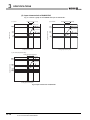
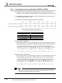
Fig. 3.3 shows a graph of the Q66AD-DG input characteristic.
2) 0 to 20mA
Practical analog input range
1) 4 to 20mA
Analog input practical range
High resolution
mode
High resolution mode
12287
12000
12287
12000
Normal resolution
mode
Digital output value
Digital output value
Normal resolution
mode
4095
4000
0
0
-96
-288
4095
4000
0
-96
-288
0 4
20
Analog input current (mA)
3) 4 to 20mA (Expanded mode)
Analog input practical range
High resolution
mode
13787
13500
12000
Digital output value
Normal resolution
mode
4595
4500
4000
0
-1000
-1096
-3000
-3288
0
0 4
20 22
Analog input current (mA)
Fig.3.3 Input characteristic of Q66AD-DG
3 - 10
3.1 Performance Specifications
3.1.2 I/O conversion characteristic
0
0
20
Analog input current (mA)
SPECIFICATIONS
{ (Gain value) - (Offset value) } 16.0mA
(4) When an analog value that exceeds the range of the digital output value is
entered, the digital output value will be fixed at the maximum or minimum
value.
0 to 20mA
4 to 20mA
4 to 20mA
(Extended mode)
User range setting
Digital output value
(High resolution mode)
Minimum
Maximum
Minimum
Maximum
-96
4095
-288
12287
-1096
4595
-3288
13787
-96
4095
-288
12287
SYSTEM
CONFIGURATION
SPECIFICATIONS
5
6
PROGRAMMING
range setting
Digital output value
(Normal resolution mode)
4
7
ONLINE MODULE
CHANGE
Analog input
3
SETUP AND
PROCEDURES
BEFORE OPERATION
(a) Gain value 24mA, offset value 0mA
(b) Use one of the following formulas according to the resolution mode to be
set.
1) Normal resolution mode
{ (Gain value) - (Offset value) } > 5.5mA
2) High resolution mode
2
UTILITY PACKAGE
(GX CONFIGURATORAD)
(1) Set within the analog input range and digital output range for each input
range.
If these ranges are exceeded, the maximum resolution and accuracy may not
fall within the performance specifications. (Avoid use shown by the dotted
lines in Fig.3.3.)
(2) Do not input an analog input current of -30mA or less and 30mA or more.
The input elements may be damaged.
(3) Set the offset/gain values for the User range setting marked within a range
which satisfies the following conditions.
OVERVIEW
1
8
TROUBLESHOOTING
3
3.1 Performance Specifications
3.1.2 I/O conversion characteristic
3 - 11
3
SPECIFICATIONS
3.1.3
Accuracy
The reference accuracy is the accuracy at the ambient temperature for offset/gain setting.
The temperature coefficient is the accuracy per temperature variation of 1°C.
The reference accuracy is the accuracy relative to the maximum digital output value.
Even if you change the offset/gain setting or input range to change the input characteristic,
the reference accuracy and temperature coefficient do not change and are kept within the
ranges given in the performance specifications.
[Example] Accuracy when the temperature changed from 25°C to 30°C
0.1% (reference accuracy) + 0.00714%/°C (temperature coefficient) 5°C (temperature
variation difference) = 0.1357%
3 - 12
3.1 Performance Specifications
3.1.3 Accuracy
3
SPECIFICATIONS
1
OVERVIEW
Function List
Table 3.3 lists the functions of the A/D converter modules.
Table3.3 Function list
Item
Section 3.4.2
Sampling processing
The A/D conversion for analog input values is performed successively for each
channel, and the digital output value is output upon each conversion.
(2)
3
Averaging processing
(a)
Time averaging
A/D conversion is averaged in terms of time on a channel basis and a digital
average value is output.
A/D conversion method
(b)
Section 3.2.1
Count averaging
A/D conversion is averaged in terms of count on a channel basis and a
digital average value is output.
(c)
4
Move averaging
The specified number of digital output values measured per sampling time
are averaged.
(3)
Primary delay filter
A digital output value is smoothed according to the preset time constant.
Maximum and minimum
(1)
values hold function
Input signal error
The maximum and minimum values of the digital output values are retained in the
module.
(1)
detection function
Section 3.2.2
A voltage or current input that is equal to or more than the input signal error
detection upper limit value, or equal to or less than the input signal error detec-
Section 3.2.3
tion lower limit value is detected.
(1)
Process alarm
A warning is output when a digital output value is equal to or more than the process alarm upper upper limit value, or equal to or less than the process alarm
Warning output function
lower lower limit value.
(2)
Section 3.2.4
Rate alarm
digital output value reaches the rate alarm upper limit value or more, or the rate
alarm lower limit value or less.
setting function
(1)
(Q66AD-DG only)
(1)
Supply power ON/OFF
function
Setting the A/D conversion starting time allows A/D conversion to be started at
the point when the output of the 2-wire transmitter stabilizes.
Section 3.2.5
The power supply to the 2-wire transmitter can be switched ON/OFF channel by
channel.
(2)
Power is supplied to channels that have input range settings of "4 to 20mA
(2-wire transmitter input): 0H", "4 to 20mA (Extended mode) (2-wire transmitter
(Q66AD-DG only)
Section 3.4.2
input): AH" or "User range setting (2-wire transmitter input): FH", and that are set
to "Enabled" in A/D conversion enable/disable setting (Un\G0).
(1)
Scaling function
Conversion of A/D conversion values to preset percentage values and loading
Section 3.2.6
into the buffer memory is available.
Programming steps for the scaling can be eliminated.
(1)
The module can be changed without the system being stopped.*1
Chapter 7
7
8
TROUBLESHOOTING
Online module change
5
6
A warning is output when the digital output value changes in a rate by which the
Conversion starting time
SPECIFICATIONS
(1)
SYSTEM
CONFIGURATION
Since the conversion time is 10ms per channel, disabling A/D conversion of
unused channels can reduce the entire conversion time.
SETUP AND
PROCEDURES
BEFORE OPERATION
(2)
2
UTILITY PACKAGE
(GX CONFIGURATORAD)
disable setting
Reference section
Specifies whether to enable or disable the A/D conversion for each channel.
PROGRAMMING
A/D conversion enable/
Function
(1)
ONLINE MODULE
CHANGE
3.2
3.2 Function List
3 - 13
3
SPECIFICATIONS
*1 If the module is changed online to a module that has no extended mode for analog input range under
the following input range settings, an intelligent function module switch error will occur.
Q68AD-G: 4 to 20mA (extended mode): AH
1 to 5V (extended mode): BH
Q66AD-DG: 4 to 20mA (extended mode) (2-wire transmitter input): AH
4 to 20mA (extended mode) (current input): CH
3 - 14
3.2 Function List
SPECIFICATIONS
1
A/D conversion is performed successively for analog input values, and the
converted digital output values are stored in the buffer memory.
The sampling processing time varies depending on the number of channels used
(number of channels set as A/D conversion enable).
Sampling processing time = No. of channels used 10 (ms)
Example) When setting 6 for the number of channels used
6 10 = 60 (ms)
(2) Averaging processing
(b) Count averaging
A/D conversion is made the preset number of times, the sum of values other than
the maximum and minimum values is averaged, and the result is stored into the
buffer memory.
The time required for the count-based average value to be stored into the buffer
memory varies depending on the number of channels used (number of channels
set as A/D conversion enable).
(No. of channels used
SETUP AND
PROCEDURES
BEFORE OPERATION
Example) When setting 6 for the number of channels used, and 500ms for the
set time
500/(6 10) = 8.333 (times) Drop the fractional part.
4
5
UTILITY PACKAGE
(GX CONFIGURATORAD)
10) (times)
6
10) (ms)
Example) When setting 5 (times) for the average processing count
5 6 10 = 50 (ms)
(c) Moving average
The specified count of digital output values imported per sampling time are averaged to find a value, which is then stored into the buffer memory.
Since average processing is performed with data shifted per sampling, the most
recent digital output value is obtainable.
PROGRAMMING
Processing count = Set time/(No. of channels used
SPECIFICATIONS
3
(a) Time averaging
A/D conversion is made for the preset period of time, the sum of values other than
the maximum and minimum values is averaged, and the result is stored into the
buffer memory.
The processing count within the set time varies depending on the number of
channels used (number of channels set as A/D conversion enable).
Processing time = Set count
2
SYSTEM
CONFIGURATION
(1) Sampling processing
OVERVIEW
A/D conversion methods
7
ONLINE MODULE
CHANGE
3.2.1
8
TROUBLESHOOTING
3
3.2 Function List
3.2.1 A/D conversion methods
3 - 15
3
SPECIFICATIONS
Moving average processing at the preset count of 4 times
A/D conversion
value
Sampling time
12000
3)
2)
4)
5)
6)
1)
7)
8)
9)
12)
10) 11)
Buffer memory
6000
First storage
Second storage
Third storage
0
Digital output value
Time [ms]
A/D conversion completed flag ON
Data transition inside buffer memory
First storage
Second storage
Third storage
1)+2)+3)+4)
2)+3)+4)+5)
3)+4)+5)+6)
4
4
4
(3) Primary delay filter
A digital value whose transient noise has been smoothed is output according to the
preset time constant.
The degree of smoothing varies with the time constant setting.
The relational expression of the time constant and digital output value is indicated
below.
[If n = 1*1]
Yn = 0
[If n = 2]
Yn = yn-1 +
[If n
t
t + TA
(yn - yn-1)
3]
Yn = Yn-1 +
t
(yn - Yn-1)
t + TA
Yn
:
Current digital output value
:
Pre-smoothing digital output value
Yn-1
:
Immediately preceding digital output Yn-1
value
yn
:
Immediately preceding
pre-smoothing digital output value
n
:
Sampling count
:
A/D conversion time (0.01
number of conversion enabled channels)(s)
TA
:
Time constant (s)
t
*1 The A/D conversion completed flag turns ON when n
3 - 16
3.2 Function List
3.2.1 A/D conversion methods
2.
SPECIFICATIONS
12000
1
10000
3
8000
0.6
6000
0.4
4000
0.2
2000
4
0
1000
Elapsed time (ms)
Analog input value
Digital output value
(time constant setting: 1000ms)
Digital output value
(moving average processing: 16 times)
Digital output value
(time constant setting: 2000ms)
6
1
12000
10000
0.8
8000
0.6
6000
0.4
4000
0.2
2000
0
0
Elapsed time (ms)
7
8
TROUBLESHOOTING
0
Digital output value
1.2
5
UTILITY PACKAGE
(GX CONFIGURATORAD)
[Example 2] Digital output value when the variation of the analog input value has a
ringing waveform
When the high resolution mode and the input range of 0 to 10V is
specified for the Q68AD-G
The variations of the digital output values at the time constant setting
of 2000ms (2s), at the time constant setting of 1000ms (1s), and at
the moving average processing of 16 times are as shown below.
PROGRAMMING
0
ONLINE MODULE
CHANGE
0
SETUP AND
PROCEDURES
BEFORE OPERATION
0.8
Digital output value
Digital output value
SPECIFICATIONS
1.2
Analog input value
Analog input value (V)
2
SYSTEM
CONFIGURATION
[Example 1] Digital output value when the analog input value varied from 0 to 1V
When the high resolution mode and the input range of 0 to 10V is
specified for the Q68AD-G
The variation of the digital output value at the time constant setting of
1000ms (1s) is as shown below.
1000ms (1s) after the analog input value has reached 1V, the digital
output value reaches 63.2% of the value attained when the sampling
processing is selected.
OVERVIEW
1
Analog input value (V)
3
3.2 Function List
3.2.1 A/D conversion methods
3 - 17
3
SPECIFICATIONS
3.2.2
Maximum and minimum values hold function
(1) The maximum and minimum values are held in the buffer memory channel by
channel.
(2) The maximum and minimum values are cleared to 0 when the maximum value/
minimum value reset request (YD) or operating condition setting request (Y9) is
turned ON, and new maximum and minimum values are stored when conversion is
started.
(3) Since the area for storing the maximum and minimum values can be rewritten with the
sequence program, the maximum and minimum values within a specific period of time
can be checked.
(4) When the scaling function is enabled, values after scaling conversion are stored as
the maximum and minimum values.
For the scaling function, refer to Section 3.2.6.
3.2.3
Input signal error detection function
(1) If the input voltage/current rose to or above the input signal error detection upper limit
value or fell to or below the lower limit value, the input signal error detection flag
(Un\G49) and input signal error detection signal (XC) turn ON and the ALM LED
flickers to indicate the error.
(2) When the input signal error detection flag (Un\G49) turns ON for a channel, a digital
output value immediately before the error detection is held for the channel, and the
A/D conversion completed flag (Un\G10) of the corresponding channel turns OFF.
(3) By bringing the analog input value within the setting range and then turning ON the
error clear request (YF), the input signal error detection flag (Un\G49) and input signal
error detection signal (XC) turn OFF.
3 - 18
3.2 Function List
3.2.2 Maximum and minimum values hold function
SPECIFICATIONS
(4) When the analog input value returns to within the setting range, A/D conversion is
resumed independently of whether the input signal error detection flag (Un\G49) and
input signal error detection signal (XC) are reset or not, the A/D conversion completed
flag (Un\G10) of the corresponding channel turns ON again after the first updating.
(The ERR. LED remains flickering.)
OVERVIEW
1
2
CH1 analog
input value
Input value
normal
3
SPECIFICATIONS
Lower limit
value
Time
4
SETUP AND
PROCEDURES
BEFORE OPERATION
CH1 input signal error detection flag
(Un\G49.b0)
Input signal error detection signal
(XC)
CH1 A/D conversion completed flag
(Un\G10.b0)
5
Error clear request (YF)
(5) This function is executed at every sampling processing.
(6) Perform the following procedure to use this function.
1) Set the input signal error detection setting value for the corresponding channel.
2) Enable the A/D conversion of the corresponding channel.
6
PROGRAMMING
3) Enable the input signal error detection of the corresponding channel.
UTILITY PACKAGE
(GX CONFIGURATORAD)
Error detection
Upper limit
value
SYSTEM
CONFIGURATION
Analog input value
4) Turn ON the operating condition setting request (Y9).
ONLINE MODULE
CHANGE
7
8
TROUBLESHOOTING
3
3.2 Function List
3.2.3 Input signal error detection function
3 - 19
3
SPECIFICATIONS
(7) How to set an input signal error detection upper/lower limit values
Set input signal error detection upper/lower limit values based on the input signal error
detection setting value (input signal error detection upper/lower limit setting values).
(Set the values in the unit of 1 (0.1%)).
The input signal error detection setting value is reflected to both the input signal error
detection upper and lower limit values by default.
To detect input signal errors using only an upper limit value or lower limit value, or to
individually set an upper limit value and a lower limit value, refer to (9) in this section.
(a) Input signal error detection upper limit value
This value is calculated as follows:
Gain value + {Full input range (Gain value - Offset value) × Input signal error
detection setting value (Input signal error detection upper limit setting value)}
A value equal to or greater than the gain value can be set.
A setting value (%) can be calculated by the following formula.
Input signal error detection
setting value
(Input signal error detection
upper limit setting value)
=
Input signal error detection
upper limit value
-
Gain value of each range
Gain value of each range
-
Offset value of each range
1000
(b) Input signal error detection lower limit value
This value is calculated as follows:
Lower limit value of the input range - {Full input range (Gain value - Offset value) ×
Input signal error detection setting value (Input signal error detection lower limit
setting value)}
A value equal to or smaller than the lower limit value of the input range can be set.
A setting value (%) can be calculated by the following formula.
Input signal error detection
setting value
(Input signal error detection
lower limit setting value)
3 - 20
=
Lower limit value of each
range
Gain value of each range
3.2 Function List
3.2.3 Input signal error detection function
-
Input signal error detection
lower limit value
Offset value of each range
1000
SPECIFICATIONS
Remark
The following table lists the lower limit value, offset value, and gain value for each
input range
2
Table3.4 The lower limit value, offset value, and gain value for each input range (Q68AD-G)
10V
0V
5V
1 to 5V
1V
5V
1 to 5V (extended mode)
1V
5V
-10 to 10V
0 to 20mA
-10V
Analog value when the digital value is:
• -4000 (normal resolution mode)
• -12000 (high resolution mode)
0mA
0V
10V
Analog value set as an
offset value by the user
Analog value set as a
gain value by the user
0mA
20mA
4 to 20mA
4mA
4mA
20mA
4 to 20mA (extended mode)
4mA
4mA
20mA
Analog value set as an
offset value by the user
Analog value set as a
gain value by the user
User range setting
Analog value when the digital value is:
• -4000 (normal resolution mode)
• -12000 (high resolution mode)
Table3.5 The lower limit value, offset value, and gain value for each input range (Q66AD-DG)
Input
Analog input range
Lower limit value
Offset value
0 to 20mA
0mA
4 to 20mA
4mA
20mA
20mA
4 to 20mA (extended mode)
4mA
20mA
User range setting
Analog value set as an offset value by the user
Analog value set as a
gain value by the user
3
SPECIFICATIONS
0V
0 to 5V
SYSTEM
CONFIGURATION
Gain value
4
SETUP AND
PROCEDURES
BEFORE OPERATION
Offset value
0 to 10V
User range setting
5
UTILITY PACKAGE
(GX CONFIGURATORAD)
Current
Lower limit value
6
PROGRAMMING
Voltage
Analog input range
7
ONLINE MODULE
CHANGE
Input
OVERVIEW
1
8
TROUBLESHOOTING
3
3.2 Function List
3.2.3 Input signal error detection function
3 - 21
3
SPECIFICATIONS
(8)Setting example of input signal error detection
Example) To detect an input signal error when the analog input value falls below
2.4mA in the channel where the input range of 4 to 20mA (extended
mode) and the normal resolution mode is set
Apply the following values to the calculation formula for an input signal error detection
lower limit value.
• Input signal error detection lower limit value: 2.4mA
• Lower limit value of the input range (offset value): 4.0mA
• Gain value: 20.0mA
Input signal error detection
setting value
=
Lower limit value of each
range
Gain value of each range
-
Input signal error detection
upper limit value
Offset value of each range
1000
Therefore, Set 100 (10.0%) as an input signal error detection setting value.
The input signal error detection values act as follows in this case. (Because of the setting value of 100 (10%), an error is detected not only at 2.4mA but also at 21.6mA.)
Input signal error detection
upper limit value
Error
21.6mA
1.6mA
(10.0 of 1.6mA)
Offset value
20mA
16mA
(Gain value - Offset value)
Gain value
4mA
1.6mA
(10.0 of 1.6mA)
2.4mA
Input signal error detection
lower limit value
3 - 22
Error
3.2 Function List
3.2.3 Input signal error detection function
3
SPECIFICATIONS
1) To detect input signal errors at a lower limit value only
• Input signal error detection extended setting: 1 (different upper/lower limit
values)
• Input signal error detection upper limit setting value: 251 (input signal error
detection disabled)
• Input signal error detection lower limit setting value: 100 (10.0%)
SYSTEM
CONFIGURATION
Example) Channel where the input range of 4 to 20mA (extended mode) and the
normal resolution mode is set
2
3
SPECIFICATIONS
(9)Specifying a condition to detect input signal errors
By setting the following buffer memory areas, input signal errors can be detected only
at an upper limit value or lower limit value, or at different upper/lower limit values.
• Input signal error detection extended/input signal error detection setting (Un\G47)
• CH input signal error detection setting value/CH input signal error detection
lower limit setting value (Un\G142 to Un\G149)
• CH input signal error detection upper limit setting value (Un\G150 to Un\G157)
The following is a setting example.
OVERVIEW
1
SETUP AND
PROCEDURES
BEFORE OPERATION
4
Input signal error detection
upper limit value
No error detected
21.6mA
1.6mA
(10.0 of 16mA)
Gain value
20mA
Offset value
4mA
1.6mA
(10.0 of 16mA)
6
2.4mA
PROGRAMMING
Error
ONLINE MODULE
CHANGE
7
8
TROUBLESHOOTING
Input signal error detection
lower limit value
UTILITY PACKAGE
(GX CONFIGURATORAD)
5
16mA
(Gain value - Offset value)
3.2 Function List
3.2.3 Input signal error detection function
3 - 23
3
SPECIFICATIONS
2) To detect input signal errors at an upper limit value only
• Input signal error detection extended setting: 1 (different upper/lower limit
values)
• Input signal error detection upper limit setting value: 100 (10.0%)
• Input signal error detection lower limit setting value: 251 (input signal error
detection disabled)
Input signal error detection
upper limit value
Error
21.6mA
1.6mA
(10.0 of 16mA)
Gain value
20mA
16mA
(Gain value - Offset value)
Offset value
4mA
1.6mA
(10.0 of 16mA)
2.4mA
Input signal error detection
lower limit value
No error
detected
3) To detect input signal errors at different upper and lower limit values
• Input signal error detection extended setting: 1 (different upper/lower limit
values)
• Input signal error detection upper limit setting value: 50 (5.0%)
• Input signal error detection lower limit setting value: 120 (12.0%)
Error
Input signal error detection
upper limit value
20.8mA
Gain value
0.8mA
(5.0 of 16mA)
20mA
16mA
(Gain value - Offset value)
Offset value
4mA
1.92mA
(12.0 of 16mA)
2.08mA
Input signal error detection
lower limit value
3 - 24
Error
3.2 Function List
3.2.3 Input signal error detection function
SPECIFICATIONS
1
(a) If the detected digital output value rose to or above the process alarm upper upper
limit value or fell to or below the process alarm lower lower limit value and entered
the warning output range zone, the warning output flag (process alarm)(Un\G50)
and warning output signal (X8) turn ON and the ALM LED is lit to indicate the
warning.
A warning will be output according to the following digital output values.
Digital value causing warning output
disable setting (Un\G53)
scaling value (Un\G54 to Un\G61)
3
(b) After a warning was output, when the digital output value reaches a value less
than the process alarm upper lower limit value, or a value more than the process
alarm lower upper limit value, "0" is stored in the corresponding bit of the warning
output flag (Un\G50) for the channel.
The warning output signal (X8) turns OFF, and the ALM LED turns OFF when the
digital output values in all channels get out of the warning output range.
Digital output value
Warning
occurrence
Upper upper
limit value
Upper lower
limit value
Warning output range
Warning output range outside
Included
Warning
occurrence
5
Warning cancel
Warning cancel
CH1 digital output
value
Warning cancel
Lower upper
limit value CH2 digital
output value
Lower lower
limit value
Warning
occurrence
6
Time
PROGRAMMING
CH1 process alarm upper limit value
(Un\G50.b0)
CH1 process alarm lower limit value
(Un\G50.b1)
7
CH2 process alarm upper limit value
(Un\G50.b2)
Warning output signal (X8)
(c) When time or count averaging is specified, this function is executed at intervals of
the preset averaging time or averaging count.
When any other A/D conversion system (sampling processing, moving average,
primary delay filter) is specified, this function is executed at intervals of the
sampling time.
(d) To use the scaling function, be sure to consider scale conversion before setting
the CH
4
UTILITY PACKAGE
(GX CONFIGURATORAD)
1: Enable CH
SPECIFICATIONS
digital output value (Un\G11 to Un\G18)
SETUP AND
PROCEDURES
BEFORE OPERATION
Item
Value set in scaling enable/ 0: Disable CH
2
SYSTEM
CONFIGURATION
(1) Process alarm
OVERVIEW
Warning output function
process alarm upper/lower limit value.
3.2 Function List
3.2.4 Warning output function
3 - 25
ONLINE MODULE
CHANGE
3.2.4
8
TROUBLESHOOTING
3
3
SPECIFICATIONS
(2) Rate alarm
(a) If the range of change in the digital output value sampled at intervals of the rate
alarm warning detection period is equal to or greater than the rate alarm upper
limit value or is equal to or less than the rate alarm lower limit value, the warning
output flag (rate alarm) (Un\G51) and warning output signal (X8) turn ON and the
ALM LED is lit to indicate the warning of the rate alarm.
(b) If, after the output of the warning, the rate fell below the rate alarm upper limit
value or rose above the rate alarm lower limit value and returned to within the setting range, "0" is stored into the bit position corresponding to the channel
number of the warning output flag (rate alarm) (Un\G51).
The warning output signal (X8) turns OFF only when all channels return to within
the setting range.
Digital output value
Rate alarm
warning detection
period
CH1 digital
output value
CH2 digital
output value
Varying rate (%) of
digital output value
Rate alarm
warning detection
period
Varying rate of
CH2 digital
output value
Time
Rate alarm
upper limit
value
Rate alarm
lower limit
value
Varying rate of
CH1 digital
output value
Time
CH1 rate alarm upper limit value
(Un\G51.b0)
CH1 rate alarm lower limit value
(Un\G51.b1)
CH2 rate alarm lower limit value
(Un\G51.b2)
Warning output signal (X8)
3 - 26
3.2 Function List
3.2.4 Warning output function
SPECIFICATIONS
(e) The rate alarm is judged by converting the rate alarm upper/lower limit value into
the digit value per rate alarm warning detection period.
The expression for the value used to make judgment per rate alarm warning
detection period is as follows.
Value used to make judgment per rate alarm warning detection period [digit]
=rate alarm upper limit value or lower limit value 0.001 maximum value of the
digital output value rate alarm warning detection period 1000
Example
3
• Rate alarm warning detection period: 10ms
are set, a value [digit] used at every rate alarm warning detection period can be
calculated as follows:
300 0.001 16000 10 1000=48(digit)
Therefore, the current value is compared with the previous value every 10ms in
channel 1, and whether a difference of 48 (digit) or more is identified between
them or not is determined.
(f) The rate alarm is useful to watch the varying rate of the digital output value in a
limited range.
1) Example of setting the rate alarm upper limit value/lower limit value when it is
desired to watch that the digital output value increases within the specified
range
Rate alarm upper limit value
5
UTILITY PACKAGE
(GX CONFIGURATORAD)
• Maximum digital output value: 16000
6
PROGRAMMING
• Upper limit value of change rate: 30%/s (300 is stored in buffer memory)
SETUP AND
PROCEDURES
BEFORE OPERATION
4
In channel 1, when the following:
Varying rate (%) of
digital output value
+30%
2
SYSTEM
CONFIGURATION
(d) The setting range of the rate alarm warning detection period is 10 to 5000ms.
When the period is set to 5000ms, the digital values are compared at intervals of 5
seconds to detect the varying rate.
SPECIFICATIONS
(c) Set the rate alarm upper limit value/lower limit value in 0.1%/s increments relative
to the maximum value (16000/12000/4000) of the digital output value.
The setting range is -32768 to 32767 (-3276.8% to 3276.7%).
OVERVIEW
1
7
+20%
ONLINE MODULE
CHANGE
Rate alarm lower limit value
0
8
Time
3.2 Function List
3.2.4 Warning output function
3 - 27
TROUBLESHOOTING
3
3
SPECIFICATIONS
2) Example of setting the rate alarm upper limit value/lower limit value when it is
desired to watch that the digital output value decreases within the specified
range
Varying rate (%) of
digital output value
0
Rate alarm upper limit value
-20%
-30%
Rate alarm lower limit value
Time
3) Example of setting the rate alarm upper limit value/lower limit value when it is
desired to watch that the digital output value increases/decreases within the
specified range
Varying rate (%) of
digital output value
Rate alarm upper limit value
+10%
0
-10%
Rate alarm lower limit value
Time
3 - 28
3.2 Function List
3.2.4 Warning output function
SPECIFICATIONS
1
(Conversion starting time) + (A/D conversion pre-processing: Approx. 150 to 165ms)
+ (A/D conversion processing: number of conversion enabled channels 10ms)
Set the A/D conversion starting time in consideration of the time necessary from
when the 2-wire transmitter powers on until its output stabilizes and the warm-up
time of the 2-wire transmitter.
[Example] When the time necessary from when the 2-wire transmitter powers on until its output stabilizes is 500ms
A/D conversion enable
When A/D conversion starting time is 0ms,
A/D conversion processing starts at this point.
Max.
20ms
When A/D conversion starting time is 500ms,
A/D conversion processing starts at this point.
Analog output of 2-wire transmitter
A/D conversion completed flag when A/D
conversion starting time is set to 500ms
(Un\G10)
A/D conversion completed flag when A/D
conversion starting time is set to 0ms
(Un\G10)
500ms
(A/D conversion
starting time)
Approx.150 to 165ms
(A/D conversion
pre-processing)
4
5
Power ON
26V power supply to 2-wire transmitter
3
Approx.150 to 165ms
(A/D conversion
pre-processing)
ON
UTILITY PACKAGE
(GX CONFIGURATORAD)
A/D conversion enable/disable setting
(Power supply to 2-wire transmitter
ON/OFF) (Un\G0)
SYSTEM
CONFIGURATION
(3) The following indicates the time until the A/D conversion completed flag (Un\G10)
turns ON when the A/D conversion starting time has been set.
SPECIFICATIONS
Conversion starting time setting (for 2-wire transmitter)
6
ON
10ms
(A/D conversion
processing time)
PROGRAMMING
(2) Set the time to the CH
(Un\G78 to Un\G83).
2
SETUP AND
PROCEDURES
BEFORE OPERATION
(1) As the A/D conversion starting time, set the "time necessary from when the used
2-wire transmitter powers on until its output stabilizes".
This setting allows A/D conversion processing to be started as soon as the output of
the 2-wire transmitter stabilizes.
OVERVIEW
Conversion starting time setting function (Q66AD-DG only)
7
10ms
(A/D conversion
processing time)
ONLINE MODULE
CHANGE
3.2.5
8
TROUBLESHOOTING
3
3.2 Function List
3.2.5 Conversion starting time setting function (Q66AD-DG only)
3 - 29
3
SPECIFICATIONS
3.2.6
Scaling Function
(1) With this function, A/D conversion values are converted to rate values and loaded into
the buffer memory.
(2) A digital value stored in CH digital output value (Un\G11 to Un\G18) is converted to
a value in the range set by CH scaling upper/lower limit value (Un\G62 to Un\G77).
The converted value is stored in CH scaling value storage area (Un\G54 to
Un\G61).
(3) The scaling function is used for processed values when using the averaging
processing or primary delay filter.
(4) The setting of CH scaling upper/lower limit value (Un\G62 to Un\G77) varies
depending on whether to use the factory default range setting or the user range
setting for the input range.
(a) When using the factory default setting for the input range
Set a value that should correspond to the upper limit of digital output as the
scaling upper limit value, and a value that should correspond to the lower limit as
the scaling lower limit value.
Example 1) Input range setting: 0 to 20mA, or 4 to
20mA (Q68AD-G, Q66AD-DG)
Digital output value
Example 2) Input range setting: -10 to 10V
(Q68AD-G)
Digital output value
Scaling
upper limit value
Scaling
upper limit value
Analig input
current (mA)
Scaling
lower limit value
Scaling
lower limit value
-
Analig input
current (mA)
(b) When using the user range setting for the input range
Set a value corresponding to the gain or offset value to the scaling upper or lower
limit value respectively.
Example 1) Gain value: 0mA, Offset value:
24mA (Q66AD-DG)
Digital output value
Example 2) Gain value: 0V, Offset value:
10V (Q68AD-G)
Digital output value
Scaling
upper limit value
Scaling
upper limit value
Scaling
lower limit value
Analig input
current (mA)
Scaling
lower limit value
3 - 30
Analig input
current (mA)
-
3.2 Function List
3.2.6 Scaling Function
SPECIFICATIONS
1
(a) When using the factory default setting for the input range
Input range: 0 to10V, 0 to 5V, 1 to 5V, 0 to 20mA, 4 to 20mA, 1 to 5V
(Extended mode), or 4 to 20mA (Extended mode)
SYSTEM
CONFIGURATION
Input range: -10 to 10V
Scaling value =
DX × (SH-SL)
DMAX - DMIN
+
SH+SL
2
3
DX
: Digital output value
DMAX
: The maximum digital output value in the input range being used
DMIN
: The minimum digital output value in the input range being used
SH
: Scaling upper limit value
SL
: Scaling lower limit value
4
Example) On the Q68AD-G, using the scaling function in High resolution mode
and in the input range of -10 to 10V
If the setting is
Scaling upper limit value, SH: 14000
Scaling lower limit value, SL : 2000
and the digital output value DX is 7500,
Scaling value =
SPECIFICATIONS
2)
DX × (SH-SL)
+ SL
DMAX
7500×(14000-2000)
(14000+2000)
+
16000-(-16000)
2
SETUP AND
PROCEDURES
BEFORE OPERATION
Scaling value =
2
5
UTILITY PACKAGE
(GX CONFIGURATORAD)
1)
OVERVIEW
(5) How to calculate a scaling value is explained below.
6
PROGRAMMING
= 10812.5....
= 10812
It omits digits below the decimal point.
ONLINE MODULE
CHANGE
7
8
TROUBLESHOOTING
3
3.2 Function List
3.2.6 Scaling Function
3 - 31
3
SPECIFICATIONS
(b) When using the user range setting for the input range
Scaling value =
DX × (SH-SL)
+ SL
DMAX
DX
: Digital output value
DMAX
:
SH
: Scaling upper limit value
SL
: Scaling lower limit value
The maximum digital output value in the input range being used
(A/D conversion value corresponding to the gain value)
Example) On the Q68AD-G, using the scaling function in High resolution mode
and in the user range setting
If the setting is
Scaling upper limit value, SH: 10000
Scaling lower limit value, SL : 2000
and the digital output value 4250 is input,
Scaling value =
4250×(10000-2000)
+ 2000
12000
= 4833.33....
= 4833
It omits digits below the decimal point.
The setting range allowed for the scaling upper and lower values is -32000 to
32000. Note that the resolution will not change even if a scaling upper/lower limit
value is set to change more than the resolution.
3 - 32
3.2 Function List
3.2.6 Scaling Function
3
SPECIFICATIONS
1
List of I/O signals
Table 3.4 lists the I/O signals of the Q68AD-G.
Table 3.5 lists the I/O signals of the Q66AD-DG.
Note that I/O numbers (X/Y) shown in this chapter and thereafter are the values when the
start I/O number for the A/D converter module is set to 0.
Table3.6 List of I/O signal (Q68AD-G)
Signal direction CPU Module
Device No. (Input)
Signal direction CPU Module
Device No. (Output)
Y0
X1
Y1
X2
Y2
X3
Y3
Use prohibited*1
X4
Use prohibited*1
Y4
X5
Y5
4
Y6
X7
High resolution mode status flag
Y7
X8
Warning output signal
Y8
X9
Operating condition setting completed flag
Y9
XA
Offset/gain setting mode flag
YA
User range writing request
XB
Channel change completed flag
YB
Channel change request
XC
Input signal error detection signal
YC
Maximum value/minimum value reset
completed flag
YD
XE
A/D conversion completed flag
YE
XF
Error flag
YF
SETUP AND
PROCEDURES
BEFORE OPERATION
X6
XD
3
SPECIFICATIONS
Module ready
Q68AD-G
Signal name
Operating condition setting request
Use prohibited*1
Maximum value/minimum value reset
5
request
UTILITY PACKAGE
(GX CONFIGURATORAD)
X0
Q68AD-G
Signal name
2
SYSTEM
CONFIGURATION
3.3.1
OVERVIEW
I/O Signals for the Programmable Controller CPU
Use prohibited*1
Error clear request
6
*1 These signals cannot be used by the user since they are for system use
only.
If these are turned ON/OFF by the sequence program, the performance
of the A/D converter module cannot be guaranteed.
PROGRAMMING
3.3
ONLINE MODULE
CHANGE
7
TROUBLESHOOTING
8
3.3 I/O Signals for the Programmable Controller CPU
3.3.1 List of I/O signals
3 - 33
3
SPECIFICATIONS
Table3.7 List of I/O signal (Q66AD-DG)
Signal direction CPU Module
Device No. (Input)
X0
Q66AD-DG
Signal name
Module ready
Signal direction CPU Module
Device No. (Output)
Y0
X1
Y1
X2
Y2
X3
Use prohibited*1
X4
Q66AD-DG
Signal name
X5
Y3
Use prohibited*1
Y4
Y5
X6
Y6
X7
High resolution mode status flag
Y7
X8
Warning output signal
Y8
X9
Operating condition setting completed flag
Y9
Operating condition setting request
XA
Offset/gain setting mode flag
YA
User range writing request
XB
Channel change completed flag
YB
Channel change request
YC
Offset/gain change request
XC
XD
Input signal error detection signal
Offset/gain change completed flag
Maximum value/minimum value reset
completed flag
YD
XE
A/D conversion completed flag
YE
XF
Error flag
YF
Maximum value/minimum value reset
request
Use prohibited*1
Error clear request
*1 These signals cannot be used by the user since they are for system use
only.
If these are turned ON/OFF by the sequence program, the performance
of the A/D converter module cannot be guaranteed.
3 - 34
3.3 I/O Signals for the Programmable Controller CPU
3.3.1 List of I/O signals
3
SPECIFICATIONS
1
OVERVIEW
Details of I/O signals
I/O signals for the A/D converter modules are explained in detail below.
(1) Input signals
2
(1)
When the programmable controller CPU is powered on or reset, this signal turns on once the
preparation for A/D conversion has been completed, and A/D conversion processing is then performed.
X0
Module ready
(2)
In either of the following states, the Module ready (X0) turns OFF.
During offset/gain setting mode (A/D conversion processing is performed.)
3
When the A/D converter module has a watchdog timer error*1
(A/D conversion processing is not performed.)
X7
High resolution
mode status flag
(1)
(1)
This turns ON when in high resolution mode.
The Warning output signal (X8) turns ON at detection of a process alarm or rate alarm.
(a)
Process alarm
1) This signal turns ON when the digital output value falls outside the setting range set to
the process alarm upper/lower limit values (Un\G86 to Un\G117) on any of the
channels enabled for A/D conversion after the process alarm function has been made
valid.
2) As soon as the digital output values return to within the setting ranges on all channels
enabled for A/D conversion, this signal turns OFF automatically and the ALM LED is
also extinguished.
(b)
Rate alarm
1) This signal turns ON when the varying rate of the digital output value falls outside the
on any of the channels enabled for A/D conversion after the rate alarm function has
been made valid.
2) As soon as the varying rates of the digital output values return to within the preset
varying ranges on all channels enabled for A/D conversion, this signal turns OFF
automatically and the ALM LED is also extinguished.
Performed by the A/D converter module
Performed by the sequence program
Warning output flag
(Un\G50, Un\G51)
0
Warning occurrence
(Process alarm, rate alarm)
5
6
0
PROGRAMMING
signal
varying rate range set to the rate alarm upper/lower limit values (Un\G122 to Un\G137)
Warning output signal (X8)
*1 A watchdog timer error occurs when the program calculations are not completed within the
scheduled time due to malfunctions of A/D converter module hardware.
When a watchdog timer error occurs, the RUN LED for the A/D converter module turns off.
7
ONLINE MODULE
CHANGE
Warning output
4
8
TROUBLESHOOTING
X8
SYSTEM
CONFIGURATION
Description
SPECIFICATIONS
Signal Name
SETUP AND
PROCEDURES
BEFORE OPERATION
Device No.
UTILITY PACKAGE
(GX CONFIGURATORAD)
3.3.2
3.3 I/O Signals for the Programmable Controller CPU
3.3.2 Details of I/O signals
3 - 35
3
SPECIFICATIONS
Device No.
Signal Name
Description
(1)
This signal is used as an interlock condition to turn ON/OFF the Operating condition setting request
(Y9) when any of the following settings has been changed.
A/D conversion enable/disable setting (Un\G0)
CH Average time/Average number of times/Moving average/Time constant settings (Un\G1 to Un\G8)
Averaging process specification (Un\G24, Un\G25)
Input signal error detection extended/input signal error detection setting (Un\G47)
Warning output settings (Un\G48)
Scaling enable/disable setting(Un\G53)
CH
scaling upper/lower limit value (Un\G62 to Un\G77)
CH
conversion starting time setting (for 2-wire transmitter) *1 (Un\G78 to Un\G83)
CH
process alarm upper/lower limit value (Un\G86 to Un\G117)
CH
rate alarm warning detection period (Un\G118 to Un\G125)
CH
rate alarm upper/lower limit value (Un\G126 to Un\G141)
CH
input signal error detection setting value/CH
input signal error detection lower limit setting
value (Un\G142 to Un\G149)
Operating
X9
condition setting
CH
(2)
input signal error detection upper limit setting value (Un\G150 to Un\G157)
When the operating condition setting completed flag (X9) is OFF, A/D conversion processing is not
performed. Under the following conditions, the operating condition setting completed flag (X9)
completed flag
turns OFF.
When operating condition setting request (Y9) is ON
Performed by the A/D converter module
Performed by the sequence program
Module ready (X0)
Operating condition
setting completed flag (X9)
Operating condition
setting request (Y9)
A/D conversion
completed flag (XE)
(3)
Digital outputs are cleared immediately after this Operating condition setting request (Y9) turns ON.
Therefore, turn ON the A/D conversion completed flag before reading digital outputs.
*1: For the Q66AD-DG only
3 - 36
3.3 I/O Signals for the Programmable Controller CPU
3.3.2 Details of I/O signals
3
SPECIFICATIONS
1
(1)
This signal is used as an interlock condition to turn ON/OFF the User range writing request (YA)
when the value at completion of offset/gain setting adjustment is registered.
(2)
Refer to Section 4.6 regarding the offset/gain settings.
2
Performed by the A/D converter module
Performed by the sequence program
OFF
SYSTEM
CONFIGURATION
Module ready (X0)
Offset/gain setting mode flag (XA)
XA
User range writing request (YA)
Offset/gain
setting mode flag
3
[In normal mode]
(1)
This signal is used as an interlock condition to turn ON/OFF the User range writing request (YA)
when the user range is restored.
(2)
Refer to Chapter 7 for the user range restoration.
Performed by the A/D converter module
Performed by the sequence program
Module ready (X0)
ON
4
Offset/gain setting mode flag (XA)
User range writing request (YA)
(1)
This signal is used as an interlock condition for setting the channel change request (YB) to ON/
OFF when changing the channel for which the offset/gain settings are to be performed.
(2)
5
Refer to Section 4.6 regarding the offset/gain settings.
6
PROGRAMMING
Channel change completed
flag (XB)
Channel change request (YB)
7
ONLINE MODULE
CHANGE
completed flag
Offset/gain setting mode
Offset/gain specifications
(Un\G22, Un\G23)
8
TROUBLESHOOTING
XB
UTILITY PACKAGE
(GX CONFIGURATORAD)
Performed by the A/D converter module
Performed by the sequence program
Channel change
OVERVIEW
Description
[In offset/gain setting mode]
SPECIFICATIONS
Signal Name
SETUP AND
PROCEDURES
BEFORE OPERATION
Device No.
3.3 I/O Signals for the Programmable Controller CPU
3.3.2 Details of I/O signals
3 - 37
3
SPECIFICATIONS
Device No.
Signal Name
Description
(1)
This signal turns ON when the analog input value falls outside the setting range set to the Input
signal error detection setting value value/input signal error detection lower limit setting value
(Un\G142 to Un\G149), Input signal error detection upper limit setting value (Un\G150 to
Un\G157) on any of the channels enabled for A/D conversion after the Input signal error detection is made valid.
(2)
When the Input signal error detection signal turns ON
1) The A/D conversion completed flag (Un\G10) of the corresponding channel turns OFF.
2) The digital output value is held as at the time of error detection.
3) The ALM LED flickers.
(3)
By bringing the analog input value within the setting range and then turning ON the Error clear
request (YF), the Input signal error detection signal (XC) turns OFF and the ALM LED is
extinguished.
(4)
When the analog input value returns to within the setting range, A/D conversion is resumed
independently of whether the Input signal error detection signal (XC) is reset or not, and after
Input signal error
the first updating, the A/D conversion completed flag (Un\G10) of the corresponding channel
detection signal
turns ON again.
The processing, such as averaging processing or primary delay filter, starts from the first time
after resumption of A/D conversion.
Performed by the A/D converter module
Performed by the sequence program
XC
Input signal error detection flag
(Un\G49)
0
Input signal error
detection
0
Input signal error detection signal
(XC)
Error clear request (YF)
(1)
This signal is used as an interlock condition to turn ON/OFF the offset/gain change request (YC)
(2)
Refer to Section 4.6 for the offset/gain setting.
when the offset/gain value is changed.
Performed by the A/D converter module
Performed by the sequence program
Offset/gain
change
completed flag*1
Offset/gain change completed flag
(XC)
Offset/gain change request (YC)
3 - 38
3.3 I/O Signals for the Programmable Controller CPU
3.3.2 Details of I/O signals
3
SPECIFICATIONS
1
This signal turns ON when the maximum value/minimum value stored at any of the buffer
memory addresses 30 to 45 (Un\G30 to Un\G45) is reset by turning ON the Maximum value/
minimum value reset request (YD).
Performed by the A/D converter module
Performed by the sequence program
Maximum value/
2
Maximum and minimum values
storage area
(Un\G30 to Un\G45)
minimum value
reset completed
SYSTEM
CONFIGURATION
XD
flag
Maximum value/minimum value
reset request (YD)
3
Maximum value/minimum value
reset completed flag (XD)
(1)
This signal turns ON when conversion for all of the channels that are conversion enabled has
been completed.
(2)
This signal or the A/D conversion completed flag (Un\G10) is used as an interlock condition to
read out the digital output value.
(3)
XE
*1When
the external supply power to the Q66AD-DG switches OFF, the A/D conversion
A/D conversion
completed flag turns OFF, and A/D conversions stop with the previous digital output values
completed flag
being held.
When the external supply power switches ON, A/D conversions resume, and as soon as all
conversion-enabled channels have completed conversions, the A/D conversion completed flag
turns ON.
The processing, such as averaging processing or primary delay filter, starts from the first time
after resumption of A/D conversion.
This signal turns ON when a write error occurs.
(2)
To clear the error code, set the error clear request (YF) to ON.
5
Performed by the A/D converter module
Performed by the sequence program
Error occurs
Error flag
6
PROGRAMMING
Error flag (XF)
Error clear request (YF)
*1: Q66AD-DG only
ONLINE MODULE
CHANGE
7
8
TROUBLESHOOTING
XF
4
UTILITY PACKAGE
(GX CONFIGURATORAD)
(1)
Error code(Un\G19)
OVERVIEW
Description
(1)
SPECIFICATIONS
Signal Name
SETUP AND
PROCEDURES
BEFORE OPERATION
Device No.
3.3 I/O Signals for the Programmable Controller CPU
3.3.2 Details of I/O signals
3 - 39
3
SPECIFICATIONS
(2) Output signals
Device No.
Signal Name
Description
(1)
Turn this signal ON when making any of the following settings valid.
A/D conversion enable/disable setting (Un\G0)
CH
Average time/Average number of times/Moving average/Time constant settings
(Un\G1 to Un\G8)
Averaging process specification (Un\G24, Un\G25)
Input signal error detection extended/input signal error detection setting (Un\G47)
Warning output settings (Un\G48)
Y9
Operating
Scaling enable/disable setting(Un\G53)
condition setting
CH
request
CH
conversion starting time setting (for 2-wire transmitter) (Un\G78 to Un\G83)
CH
process alarm upper/lower limit value (Un\G86 to Un\G117)
scaling upper/lower limit value(Un\G62 to Un\G72)
CH
rate alarm warning detection period (Un\G118 to Un\G125)
CH
rate alarm upper/lower limit value (Un\G126 to Un\G141)
CH
input signal error detection setting value/CH input signal error detection lower limit setting
value (Un\G142 to Un\G149)
CH
input signal error detection upper limit setting value (Un\G150 to Un\G157)
(2) Refer to the X9 column for ON/OFF timing.
[In offset/gain setting mode]
(1)
This turns ON when the value for the adjusted offset/gain settings are registered in the A/D
(2)
Refer to the XA column for ON/OFF timing.
converter module.
YA
User range writing
request
Refer to Section 4.6 for offset/gain settings.
[In normal mode]
(1)
This signal turns ON when the user range is restored.
(2)
Refer to the field of XA for the ON/OFF timing.
(1)
This turns ON when changing the channel for which offset/gain settings are to be performed.
(2)
Refer to the XB column for ON/OFF timing.
(1)
Turn this signal ON when changing the offset/gain value.
(2)
Refer to the field of XC for the ON/OFF timing.
(1)
Turning ON the Maximum value/minimum value reset request (YD) clears the maximum value/
reset request
(2)
Refer to the XD column for ON/OFF timing.
Error clear
(1)
Turn this signal ON when clearing a write error or input signal error.
request
(2)
Refer to the field of XF or XC for the ON/OFF timing.
Refer to Chapter 7 for user range restoration.
YB
YC
Channel change
request
Offset/gain
change request*1
Maximum value/
YD
YF
Refer to Section 4.6 for offset/gain settings.
Refer to Section 4.6 for the offset/gain setting.
minimum value
minimum value stored at any of the buffer memory addresses 30 to 45 (Un\G30 to Un\G45).
*1: Q66AD-DG only
3 - 40
3.3 I/O Signals for the Programmable Controller CPU
3.3.2 Details of I/O signals
SPECIFICATIONS
When the User range writing request (YA) is turned ON in the normal mode with
A/D conversion enabled, the A/D converter module restores the user range.
Offset/gain setting mode flag (XA)
OVERVIEW
1
User range writing request (YA)
During restoration
User range restoration processing
Restoration
completed
A/D conversion completed flag
(Un\G10)
SYSTEM
CONFIGURATION
2
Power of 2-wire transmitter
Power ON
Power ON
Power OFF
During user range restoration :
:
4
5
UTILITY PACKAGE
(GX CONFIGURATORAD)
After user range restoration
A/D conversion stop, A/D conversion
completed flag (Un\G10) OFF, previous digital
output value held, power of 2-wire transmitter
OFF (Q66AD-DG only)
A/D conversion resumed (when user range
setting is used, A/D conversion is resumed at
the restored offset/gain setting value.)
SETUP AND
PROCEDURES
BEFORE OPERATION
Digital output value
(Un\G11 to Un\G18)
SPECIFICATIONS
3
PROGRAMMING
6
ONLINE MODULE
CHANGE
7
8
TROUBLESHOOTING
3
3.3 I/O Signals for the Programmable Controller CPU
3.3.2 Details of I/O signals
3 - 41
3
SPECIFICATIONS
3.4
Buffer Memory
3.4.1
Buffer memory assignment
This section describes the buffer memory assignments of the A/D converter modules.
3 - 42
3.4 Buffer Memory
3.4.1 Buffer memory assignment
SPECIFICATIONS
1
Table3.8 Buffer memory assignment of Q68AD-G (1/6)
1H
1
2H
2
3H
3
4H
4
5H
5
6H
6
7H
7
8H
8
A/D conversion enable/disable setting
CH1 Average time/Average number of times/
Moving average/Time constant settings
CH2 Average time/Average number of times/
Moving average/Time constant settings
CH3 Average time/Average number of times/
Moving average/Time constant settings
CH4 Average time/Average number of times/
Moving average/Time constant settings
CH5 Average time/Average number of times/
Moving average/Time constant settings
CH6 Average time/Average number of times/
Moving average/Time constant settings
CH7 Average time/Average number of times/
Moving average/Time constant settings
CH8 Average time/Average number of times/
Moving average/Time constant settings
R/W*1
Reference
0000H
R/W*2
Section 3.4.2
0
R/W*2
0
R/W*2
0
R/W*2
0
R/W*2
0
R/W*2
0
R/W*2
0
R/W*2
0
R/W*2
4
Section 3.4.3
5
9H
9
System area
—
—
—
AH
10
A/D conversion completed flag
0
R
Section 3.4.4
11
CH1 Digital output value
0
R
12
CH2 Digital output value
0
R
DH
13
CH3 Digital output value
0
R
EH
14
CH4 Digital output value
0
R
FH
15
CH5 Digital output value
0
R
10H
16
CH6 Digital output value
0
R
11H
17
CH7 Digital output value
0
R
12H
18
CH8 Digital output value
0
R
13H
19
Error code
0
R
14H
20
Setting range(CH1 to CH4)
0
R
15H
21
Setting range(CH5 to CH8)
0
R
16H
22
Offset/gain setting mode offset specification
0
R/W
17H
23
Offset/gain setting mode gain specification
0
R/W
18H
24
Averaging process specification (CH1 to CH4)
0
R/W*2
19H
25
Averaging process specification (CH5 to CH8)
0
R/W*2
Section 3.4.5
Section 3.4.7
Section 3.4.8
7
Section 3.4.6
Section 3.4.9
*1 Indicates whether reading from and writing to a sequence program are enabled.
R : Read enabled
W : Write enabled
*2 When writing data to the buffer memory, always use the interlock condition (buffer memory write
condition) of the following I/O signals.
Buffer memory writing condition
Y9
X9
Writing Operating Operating
request condition condition
setting
setting
request completed
flag
MOV
3.4 Buffer Memory
3.4.1 Buffer memory assignment
6
PROGRAMMING
BH
CH
3
SPECIFICATIONS
0
Default
SETUP AND
PROCEDURES
BEFORE OPERATION
0H
Description
UTILITY PACKAGE
(GX CONFIGURATORAD)
Decimal
3 - 43
ONLINE MODULE
CHANGE
Address
Hexadecimal
2
SYSTEM
CONFIGURATION
Do not write data from system area or sequence program to the buffer memory
area where writing is disabled.
Doing so may cause malfunction.
OVERVIEW
(1) Buffer memory assignment of Q68AD-G
8
TROUBLESHOOTING
3
3
SPECIFICATIONS
Table3.8 Buffer memory assignment of Q68AD-G (2/6)
Address
Hexadecimal
Decimal
1AH
26
Default
R/W*1
Reference
System area
—
—
—
R/W
Description
to
to
1DH
29
1EH
30
CH1 Maximum value
0
1FH
31
CH1 Minimum value
0
R/W
20H
32
CH2 Maximum value
0
R/W
21H
33
CH2 Minimum value
0
R/W
22H
34
CH3 Maximum value
0
R/W
23H
35
CH3 Minimum value
0
R/W
24H
36
CH4 Maximum value
0
R/W
25H
37
CH4 Minimum value
0
R/W
26H
38
CH5 Maximum value
0
R/W
27H
39
CH5 Minimum value
0
R/W
28H
40
CH6 Maximum value
0
R/W
29H
41
CH6 Minimum value
0
R/W
2AH
42
CH7 Maximum value
0
R/W
Section 3.4.10
2BH
43
CH7 Minimum value
0
R/W
2CH
44
CH8 Maximum value
0
R/W
2DH
45
CH8 Minimum value
0
R/W
2EH
46
System area
—
—
—
00FFH
R/W*2
Section 3.4.11
FFFFH
R/W*2
Section 3.4.12
0
R
Section 3.4.13
Input signal error detection extended/input signal error
2FH
47
30H
48
Warning output setting
31H
49
Input signal error detection flag
32H
50
Warning output flag (Process alarm)
0
R
33H
51
Warning output flag (Rate alarm)
0
R
34H
52
System area
—
—
35H
53
Scaling enable/disable setting
36H
54
CH1 Scaling value
0
R
37H
55
CH2 Scaling value
0
R
38H
56
CH3 Scaling value
0
R
39H
57
CH4 Scaling value
0
R
3AH
58
CH5 Scaling value
0
R
detection setting
00FFH
R/W
Section 3.4.14
—
*2
3BH
59
CH6 Scaling value
0
R
3CH
60
CH7 Scaling value
0
R
3DH
61
CH8 Scaling value
0
R
3EH
62
CH1 Scaling lower limit value
0
R/W*2
3FH
63
CH1 Scaling upper limit value
0
R/W*2
40H
64
CH2 Scaling lower limit value
0
R/W*2
41H
65
CH2 Scaling upper limit value
0
R/W*2
42H
66
CH3 Scaling lower limit value
0
R/W*2
43H
67
CH3 Scaling upper limit value
0
R/W*2
Section 3.4.15
Section 3.4.16
Section 3.4.17
*1 Indicates whether reading from and writing to a sequence program are enabled.
R : Read enabled
W : Write enabled
*2 When writing data to the buffer memory, always use the interlock condition (buffer memory write
condition) of the following I/O signals.
Buffer memory writing condition
Y9
X9
Writing Operating Operating
request condition condition
setting
setting
request completed
flag
3 - 44
3.4 Buffer Memory
3.4.1 Buffer memory assignment
MOV
SPECIFICATIONS
1
0
R/W*2
69
CH4 Scaling upper limit value
0
R/W*2
46H
70
CH5 Scaling lower limit value
0
R/W*2
47H
71
CH5 Scaling upper limit value
0
R/W*2
48H
72
CH6 Scaling lower limit value
0
R/W*2
49H
73
CH6 Scaling upper limit value
0
R/W*2
4AH
74
CH7 Scaling lower limit value
0
R/W*2
4BH
75
CH7 Scaling upper limit value
0
R/W*2
4CH
76
CH8 Scaling lower limit value
0
R/W*2
4DH
77
CH8 Scaling upper limit value
0
R/W*2
4EH
78
System area
—
—
to
to
55H
85
56H
86
CH1 Process alarm lower lower limit value
0
R/W*2
57H
87
CH1 Process alarm lower upper limit value
0
R/W*2
58H
88
CH1 Process alarm upper lower limit value
0
R/W*2
59H
89
CH1 Process alarm upper upper limit value
0
R/W*2
5AH
90
CH2 Process alarm lower lower limit value
0
R/W*2
*2
2
Section 3.4.17
3
—
5BH
91
CH2 Process alarm lower upper limit value
0
R/W
5CH
92
CH2 Process alarm upper lower limit value
0
R/W*2
5DH
93
CH2 Process alarm upper upper limit value
0
R/W*2
5EH
94
CH3 Process alarm lower lower limit value
0
R/W*2
5FH
95
CH3 Process alarm lower upper limit value
0
R/W*2
60H
96
CH3 Process alarm upper lower limit value
0
R/W*2
61H
97
CH3 Process alarm upper upper limit value
0
R/W*2
62H
98
CH4 Process alarm lower lower limit value
0
R/W*2
63H
99
CH4 Process alarm lower upper limit value
0
R/W*2
64H
100
CH4 Process alarm upper lower limit value
0
R/W*2
65H
101
CH4 Process alarm upper upper limit value
0
R/W*2
66H
102
CH5 Process alarm lower lower limit value
0
R/W*2
67H
103
CH5 Process alarm lower upper limit value
0
R/W*2
68H
104
CH5 Process alarm upper lower limit value
0
R/W*2
69H
105
CH5 Process alarm upper upper limit value
0
R/W*2
6AH
106
CH6 Process alarm lower lower limit value
0
R/W*2
6BH
107
CH6 Process alarm lower upper limit value
0
R/W*2
6CH
108
CH6 Process alarm upper lower limit value
0
R/W*2
6DH
109
CH6 Process alarm upper upper limit value
0
R/W*2
6EH
110
CH7 Process alarm lower lower limit value
0
R/W*2
6FH
111
CH7 Process alarm lower upper limit value
0
R/W*2
70H
112
CH7 Process alarm upper lower limit value
0
R/W*2
71H
113
CH7 Process alarm upper upper limit value
0
R/W*2
4
SETUP AND
PROCEDURES
BEFORE OPERATION
45H
5
Section 3.4.19
6
PROGRAMMING
68
7
*1 Indicates whether reading from and writing to a sequence program are enabled.
R : Read enabled
W : Write enabled
*2 When writing data to the buffer memory, always use the interlock condition (buffer memory write
condition) of the following I/O signals.
8
Buffer memory writing condition
Y9
X9
Writing Operating Operating
request condition condition
setting
setting
request completed
flag
SYSTEM
CONFIGURATION
CH4 Scaling lower limit value
44H
Reference
SPECIFICATIONS
R/W*1
Description
UTILITY PACKAGE
(GX CONFIGURATORAD)
Default
Decimal
ONLINE MODULE
CHANGE
Address
Hexadecimal
OVERVIEW
Table3.8 Buffer memory assignment of Q68AD-G (3/6)
TROUBLESHOOTING
3
MOV
3.4 Buffer Memory
3.4.1 Buffer memory assignment
3 - 45
3
SPECIFICATIONS
Table3.8 Buffer memory assignment of Q68AD-G (4/6)
Address
Default
R/W*1
CH8 Process alarm lower lower limit value
0
R/W*2
115
CH8 Process alarm lower upper limit value
0
R/W*2
74H
116
CH8 Process alarm upper lower limit value
0
R/W*2
75H
117
CH8 Process alarm upper upper limit value
0
R/W*2
76H
118
CH1 Rate alarm warning detection period
0
R/W*2
77H
119
CH2 Rate alarm warning detection period
0
R/W*2
78H
120
CH3 Rate alarm warning detection period
0
R/W*2
79H
121
CH4 Rate alarm warning detection period
0
R/W*2
7AH
122
CH5 Rate alarm warning detection period
0
R/W*2
Hexadecimal
Decimal
72H
114
73H
Description
7BH
123
CH6 Rate alarm warning detection period
0
R/W*2
7CH
124
CH7 Rate alarm warning detection period
0
R/W*2
7DH
125
CH8 Rate alarm warning detection period
0
R/W*2
7EH
126
CH1 Rate alarm upper limit value
0
R/W*2
7FH
127
CH1 Rate alarm lower limit value
0
R/W*2
80H
128
CH2 Rate alarm upper limit value
0
R/W*2
81H
129
CH2 Rate alarm lower limit value
0
R/W*2
82H
130
CH3 Rate alarm upper limit value
0
R/W*2
83H
131
CH3 Rate alarm lower limit value
0
R/W*2
84H
132
CH4 Rate alarm upper limit value
0
R/W*2
85H
133
CH4 Rate alarm lower limit value
0
R/W*2
86H
134
CH5 Rate alarm upper limit value
0
R/W*2
87H
135
CH5 Rate alarm lower limit value
0
R/W*2
88H
136
CH6 Rate alarm upper limit value
0
R/W*2
89H
137
CH6 Rate alarm lower limit value
0
R/W*2
8AH
138
CH7 Rate alarm upper limit value
0
R/W*2
8BH
139
CH7 Rate alarm lower limit value
0
R/W*2
8CH
140
CH8 Rate alarm upper limit value
0
R/W*2
8DH
141
CH8 Rate alarm lower limit value
0
R/W*2
50
R/W*2
50
R/W*2
50
R/W*2
50
R/W*2
50
R/W*2
50
R/W*2
8EH
142
8FH
143
90H
144
91H
145
92H
146
93H
147
CH1 Input signal error detection setting value/CH1 Input
signal error detection lower limit setting value
CH2 Input signal error detection setting value/CH2 Input
signal error detection lower limit setting value
CH3 Input signal error detection setting value/CH3 Input
signal error detection lower limit setting value
CH4 Input signal error detection setting value/CH4 Input
signal error detection lower limit setting value
CH5 Input signal error detection setting value/CH5 Input
signal error detection lower limit setting value
CH6 Input signal error detection setting value/CH6 Input
signal error detection lower limit setting value
Reference
Section 3.4.19
Section 3.4.20
Section 3.4.21
Section 3.4.22
*1 Indicates whether reading from and writing to a sequence program are enabled.
R : Read enabled
W : Write enabled
*2 When writing data to the buffer memory, always use the interlock condition (buffer memory write
condition) of the following I/O signals.
Buffer memory writing condition
Y9
X9
Writing Operating Operating
request condition condition
setting
setting
request completed
flag
MOV
*3 Areas used to restore the User range settings offset/gain values when the module is replaced online.
Refer to Chapter 7 for details of online module change.
3 - 46
3.4 Buffer Memory
3.4.1 Buffer memory assignment
SPECIFICATIONS
1
Table3.8 Buffer memory assignment of Q68AD-G (5/6)
R/W*1
50
R/W*2
50
R/W*2
2
CH1 Input signal error detection upper limit setting value
50
R/W*2
151
CH2 Input signal error detection upper limit setting value
50
R/W*2
98H
152
CH3 Input signal error detection upper limit setting value
50
R/W*2
99H
153
CH4 Input signal error detection upper limit setting value
50
R/W*2
9AH
154
CH5 Input signal error detection upper limit setting value
50
R/W*2
9BH
155
CH6 Input signal error detection upper limit setting value
50
R/W*2
95H
149
96H
150
97H
CH7 Input signal error detection setting value/CH7 Input
signal error detection lower limit setting value
CH8 Input signal error detection setting value/CH8 Input
signal error detection lower limit setting value
Section 3.4.22
3
9CH
156
CH7 Input signal error detection upper limit setting value
50
R/W*2
9DH
157
CH8 Input signal error detection upper limit setting value
50
R/W*2
9EH
158
9FH
159
Mode switching setting
0
R/W
Section 3.4.23
A0H
160
System area
—
—
—
0
Section 3.4.24
to
C7H
199
C8H
200
C9H
201
Save data classification setting*3
System area
—
R/W
—
CAH
202
CH1 Factory default offset value*3
0
R/W
CBH
203
CH1 Factory default gain value*3
CCH
204
CH2 Factory default offset
CDH
205
CH2 Factory default gain value*3
CEH
206
CH3 Factory default offset value
CFH
207
CH3 Factory default gain value*3
D0H
208
D1H
209
D2H
210
D3H
211
value*3
*3
0
R/W
0
R/W
0
R/W
0
R/W
0
R/W
CH4 Factory default offset value
0
R/W
CH4 Factory default gain value*3
0
R/W
CH5 Factory default offset value
0
R/W
CH5 Factory default gain value*3
0
R/W
*3
*3
value*3
D4H
212
CH6 Factory default offset
0
R/W
D5H
213
CH6 Factory default gain value*3
0
R/W
D6H
214
CH7 Factory default offset value*3
0
R/W
D7H
215
CH7 Factory default gain value*3
0
R/W
0
R/W
0
R/W
value*3
D8H
216
CH8 Factory default offset
D9H
217
CH8 Factory default gain value*3
—
5
Section 3.4.25
6
*1 Indicates whether reading from and writing to a sequence program are enabled.
R : Read enabled
W : Write enabled
*2 When writing data to the buffer memory, always use the interlock condition (buffer memory write
condition) of the following I/O signals.
Buffer memory writing condition
Y9
X9
Writing Operating Operating
request condition condition
setting
setting
request completed
flag
4
PROGRAMMING
to
SPECIFICATIONS
148
Reference
SETUP AND
PROCEDURES
BEFORE OPERATION
94H
Description
UTILITY PACKAGE
(GX CONFIGURATORAD)
Decimal
MOV
7
ONLINE MODULE
CHANGE
Hexadecimal
SYSTEM
CONFIGURATION
Default
OVERVIEW
Address
8
*3 Areas used to restore the User range settings offset/gain values when the module is replaced
online.
Refer to Chapter 7 for details of online module change.
3.4 Buffer Memory
3.4.1 Buffer memory assignment
3 - 47
TROUBLESHOOTING
3
3
SPECIFICATIONS
Table3.8 Buffer memory assignment of Q68AD-G (6/6)
Address
Hexadecimal
Decimal
DAH
218
DBH
219
Default
R/W*1
CH1 User range settings offset value*3
0
R/W
CH1 User range settings gain value*3
0
R/W
0
R/W
0
R/W
0
R/W
0
R/W
0
R/W
0
R/W
Description
*3
DCH
220
CH2 User range settings offset value
DDH
221
CH2 User range settings gain value*3
value*3
DEH
222
DFH
223
CH3 User range settings gain
E0H
224
CH4 User range settings offset value*3
E1H
225
CH4 User range settings gain value
E2H
226
CH5 User range settings offset value*3
0
R/W
E3H
227
CH5 User range settings gain value*3
0
R/W
0
R/W
0
R/W
0
R/W
0
R/W
0
R/W
0
R/W
CH3 User range settings offset
value*3
*3
value*3
E4H
228
E5H
229
CH6 User range settings gain
E6H
230
CH7 User range settings offset value*3
CH6 User range settings offset
value*3
value*3
E7H
231
CH7 User range settings gain
E8H
232
CH8 User range settings offset value*3
E9H
233
CH8 User range settings gain
value*3
Reference
Section 3.4.25
*1 Indicates whether reading from and writing to a sequence program are enabled.
R : Read enabled
W : Write enabled
*2 When writing data to the buffer memory, always use the interlock condition (buffer memory write
condition) of the following I/O signals.
Buffer memory writing condition
Y9
X9
Writing Operating Operating
request condition condition
setting
setting
request completed
flag
MOV
*3 Areas used to restore the User range settings offset/gain values when the module is replaced online.
Refer to Chapter 7 for details of online module change.
3 - 48
3.4 Buffer Memory
3.4.1 Buffer memory assignment
SPECIFICATIONS
1
Reference
0
003FH
R/W*2
Section 3.4.2
1H
1
0
R/W*2
2H
2
0
R/W*2
3H
3
0
R/W*2
4H
4
0
R/W*2
5H
5
0
R/W*2
6H
6
0
R/W*2
System area
—
—
—
Section 3.4.4
A/D conversion enable/disable setting
CH1 Average time/Average number of times/
Moving average/Time constant settings
CH2 Average time/Average number of times/
Moving average/Time constant settings
CH3 Average time/Average number of times/
Moving average/Time constant settings
CH4 Average time/Average number of times/
Moving average/Time constant settings
CH5 Average time/Average number of times/
Moving average/Time constant settings
CH6 Average time/Average number of times/
Moving average/Time constant settings
Section 3.4.3
7H
7
to
to
9H
9
AH
10
A/D conversion completed flag
0
R
BH
11
CH1 Digital output value
0
R
CH
12
CH2 Digital output value
0
R
DH
13
CH3 Digital output value
0
R
EH
14
CH4 Digital output value
0
R
Section 3.4.5
FH
15
CH5 Digital output value
0
R
10H
16
CH6 Digital output value
0
R
11H
17
12H
18
System area
—
—
—
13H
19
Error code
0
R
Section 3.4.6
14H
20
Setting range(CH1 to CH4)
0
R
15H
21
Setting range(CH5,CH6)
0
R
16H
22
Offset/gain setting mode offset specification
0
R/W
17H
23
Offset/gain setting mode gain specification
0
R/W
18H
24
Averaging process specification (CH1 to CH4)
0
R/W*2
0
*2
19H
25
Averaging process specification (CH5 to CH6)
R/W
4
5
6
Section 3.4.7
Section 3.4.8
Section 3.4.9
*1 Indicates whether reading from and writing to a sequence program are enabled.
R : Read enabled
W : Write enabled
*2 When writing data to the buffer memory, always use the interlock condition (buffer memory write
condition) of the following I/O signals.
7
8
Buffer memory writing condition
Y9
X9
Writing Operating Operating
request condition condition
setting
setting
request completed
flag
3
PROGRAMMING
0H
SYSTEM
CONFIGURATION
R/W*1
SPECIFICATIONS
Default
Description
ONLINE MODULE
CHANGE
Address
Hexadecimal Decimal
SETUP AND
PROCEDURES
BEFORE OPERATION
Table3.9 Buffer memory assignment of Q66AD-DG (1/5)
2
UTILITY PACKAGE
(GX CONFIGURATORAD)
Do not write data from system area or sequence program to the buffer memory
area where writing is disabled.
Doing so may cause malfunction.
OVERVIEW
(2) Buffer memory assignment of Q66AD-DG
MOV
3.4 Buffer Memory
3.4.1 Buffer memory assignment
TROUBLESHOOTING
3
3 - 49
3
SPECIFICATIONS
Table3.9 Buffer memory assignment of Q66AD-DG (2/5)
Address
Default
R/W*1
Reference
System area
—
—
—
R/W
Description
Hexadecimal Decimal
1AH
26
to
to
1DH
29
1EH
30
CH1 Maximum value
0
1FH
31
CH1 Minimum value
0
R/W
20H
32
CH2 Maximum value
0
R/W
21H
33
CH2 Minimum value
0
R/W
22H
34
CH3 Maximum value
0
R/W
23H
35
CH3 Minimum value
0
R/W
24H
36
CH4 Maximum value
0
R/W
25H
37
CH4 Minimum value
0
R/W
26H
38
CH5 Maximum value
0
R/W
27H
39
CH5 Minimum value
0
R/W
28H
40
CH6 Maximum value
0
R/W
29H
41
CH6 Minimum value
0
R/W
2AH
42
System area
—
—
—
003FH
R/W*2
Section 3.4.11
3F3FH
R/W*2
Section 3.4.12
0
R
Section 3.4.13
to
to
2EH
46
2FH
47
30H
48
Warning output setting
31H
49
Input signal error detection flag
32H
50
Warning output flag (Process alarm)
0
R
33H
51
Warning output flag (Rate alarm)
0
R
34H
52
System area
35H
53
Scaling enable/disable setting
36H
54
37H
55
38H
Input signal error detection extended/input signal error
detection setting
Section 3.4.10
Section 3.4.14
—
—
—
003FH
R/W*2
Section 3.4.15
CH1 Scaling value
0
R
CH2 Scaling value
0
R
56
CH3 Scaling value
0
R
39H
57
CH4 Scaling value
0
R
3AH
58
CH5 Scaling value
0
R
3BH
59
CH6 Scaling value
0
R
3CH
60
3DH
61
System area
—
—
3EH
62
CH1 Scaling lower limit value
0
R/W*2
3FH
63
CH1 Scaling upper limit value
0
R/W*2
40H
64
CH2 Scaling lower limit value
0
R/W*2
41H
65
CH2 Scaling upper limit value
0
R/W*2
42H
66
CH3 Scaling lower limit value
0
R/W*2
43H
67
CH3 Scaling upper limit value
0
R/W*2
44H
68
CH4 Scaling lower limit value
0
R/W*2
45H
69
CH4 Scaling upper limit value
0
R/W*2
Section 3.4.16
—
Section 3.4.17
*1 Indicates whether reading from and writing to a sequence program are enabled.
R : Read enabled
W : Write enabled
*2 When writing data to the buffer memory, always use the interlock condition (buffer memory write
condition) of the following I/O signals.
Buffer memory writing condition
Y9
X9
Writing Operating Operating
request condition condition
setting
setting
request completed
flag
3 - 50
3.4 Buffer Memory
3.4.1 Buffer memory assignment
MOV
SPECIFICATIONS
1
0
R/W*2
CH6 Scaling lower limit value
0
R/W*2
CH6 Scaling upper limit value
0
R/W*2
System area
—
—
47H
71
48H
72
49H
73
4AH
74
to
to
4DH
77
4EH
78
CH1 Conversion starting time setting (for 2-wire transmitter)
30
R/W*2
4FH
79
CH2 Conversion starting time setting (for 2-wire transmitter)
30
R/W*2
50H
80
CH3 Conversion starting time setting (for 2-wire transmitter)
30
R/W*2
51H
81
CH4 Conversion starting time setting (for 2-wire transmitter)
30
R/W*2
52H
82
CH5 Conversion starting time setting (for 2-wire transmitter)
30
R/W*2
53H
83
CH6 Conversion starting time setting (for 2-wire transmitter)
30
R/W*2
54H
84
55H
85
System area
—
—
56H
86
CH1 Process alarm lower lower limit value
0
R/W*2
57H
87
CH1 Process alarm lower upper limit value
0
R/W*2
58H
88
CH1 Process alarm upper lower limit value
0
R/W*2
59H
89
CH1 Process alarm upper upper limit value
0
R/W*2
5AH
90
CH2 Process alarm lower lower limit value
0
R/W*2
5BH
91
CH2 Process alarm lower upper limit value
0
R/W*2
5CH
92
CH2 Process alarm upper lower limit value
0
R/W*2
5DH
93
CH2 Process alarm upper upper limit value
0
R/W*2
5EH
94
CH3 Process alarm lower lower limit value
0
R/W*2
5FH
95
CH3 Process alarm lower upper limit value
0
R/W*2
60H
96
CH3 Process alarm upper lower limit value
0
R/W*2
61H
97
CH3 Process alarm upper upper limit value
0
R/W*2
62H
98
CH4 Process alarm lower lower limit value
0
R/W*2
63H
99
CH4 Process alarm lower upper limit value
0
R/W*2
64H
100
CH4 Process alarm upper lower limit value
0
R/W*2
65H
101
CH4 Process alarm upper upper limit value
0
R/W*2
66H
102
CH5 Process alarm lower lower limit value
0
R/W*2
67H
103
CH5 Process alarm lower upper limit value
0
R/W*2
68H
104
CH5 Process alarm upper lower limit value
0
R/W*2
69H
105
CH5 Process alarm upper upper limit value
0
R/W*2
106
CH6 Process alarm lower lower limit value
0
R/W*2
6BH
107
CH6 Process alarm lower upper limit value
0
R/W*2
6CH
108
CH6 Process alarm upper lower limit value
0
R/W*2
6DH
109
CH6 Process alarm upper upper limit value
0
R/W*2
6EH
110
to
to
System area
—
—
75H
117
6AH
Section 3.4.17
—
Section 3.4.18
—
5
Section 3.4.19
6
7
—
Buffer memory writing condition
Y9
X9
MOV
3.4 Buffer Memory
3.4.1 Buffer memory assignment
3
4
*1 Indicates whether reading from and writing to a sequence program are enabled.
R : Read enabled
W : Write enabled
*2 When writing data to the buffer memory, always use the interlock condition (buffer memory write
condition) of the following I/O signals.
Writing Operating Operating
request condition condition
setting
setting
request completed
flag
2
SYSTEM
CONFIGURATION
CH5 Scaling upper limit value
CH5 Scaling lower limit value
SPECIFICATIONS
R/W*2
70
SETUP AND
PROCEDURES
BEFORE OPERATION
0
46H
Reference
UTILITY PACKAGE
(GX CONFIGURATORAD)
R/W*1
PROGRAMMING
Default
Description
Decimal
3 - 51
ONLINE MODULE
CHANGE
Address
Hexadecimal
OVERVIEW
Table3.9 Buffer memory assignment of Q66AD-DG (3/5)
8
TROUBLESHOOTING
3
3
SPECIFICATIONS
Table3.9 Buffer memory assignment of Q66AD-DG (4/5)
Address
Description
Hexadecimal Decimal
Default
R/W*1
76H
118
CH1 Rate alarm warning detection period
0
R/W*2
77H
119
CH2 Rate alarm warning detection period
0
R/W*2
78H
120
CH3 Rate alarm warning detection period
0
R/W*2
79H
121
CH4 Rate alarm warning detection period
0
R/W*2
7AH
122
CH5 Rate alarm warning detection period
0
R/W*2
7BH
123
CH6 Rate alarm warning detection period
0
R/W*2
7CH
124
7DH
125
System area
—
—
7EH
126
CH1 Rate alarm upper limit value
0
R/W*2
7FH
127
CH1 Rate alarm lower limit value
0
R/W*2
80H
128
CH2 Rate alarm upper limit value
0
R/W*2
81H
129
CH2 Rate alarm lower limit value
0
R/W*2
82H
130
CH3 Rate alarm upper limit value
0
R/W*2
83H
131
CH3 Rate alarm lower limit value
0
R/W*2
84H
132
CH4 Rate alarm upper limit value
0
R/W*2
85H
133
CH4 Rate alarm lower limit value
0
R/W*2
86H
134
CH5 Rate alarm upper limit value
0
R/W*2
87H
135
CH5 Rate alarm lower limit value
0
R/W*2
88H
136
CH6 Rate alarm upper limit value
0
R/W*2
89H
137
CH6 Rate alarm lower limit value
0
R/W*2
8AH
138
System area
—
—
50
R/W*2
50
R/W*2
50
R/W*2
50
R/W*2
50
R/W*2
50
R/W*2
System area
—
—
to
to
8DH
141
8EH
142
8FH
143
90H
144
91H
145
92H
146
93H
147
94H
148
95H
149
96H
150
CH1 Input signal error detection upper limit setting value
50
R/W*2
97H
151
CH2 Input signal error detection upper limit setting value
50
R/W*2
98H
152
CH3 Input signal error detection upper limit setting value
50
R/W*2
CH1 Input signal error detection setting value/CH1 Input
signal error detection lower limit setting value
CH2 Input signal error detection setting value/CH2 Input
signal error detection lower limit setting value
CH3 Input signal error detection setting value/CH3 Input
signal error detection lower limit setting value
CH4 Input signal error detection setting value/CH4 Input
signal error detection lower limit setting value
CH5 Input signal error detection setting value/CH5 Input
signal error detection lower limit setting value
CH6 Input signal error detection setting value/CH6 Input
signal error detection lower limit setting value
Reference
Section 3.4.20
—
Section 3.4.21
—
Section 3.4.22
—
Section 3.4.22
*1 Indicates whether reading from and writing to a sequence program are enabled.
R : Read enabled
W : Write enabled
*2 When writing data to the buffer memory, always use the interlock condition (buffer memory write condition) of the following I/O signals
Buffer memory writing condition
Y9
X9
Writing Operating Operating
request condition condition
setting
setting
request completed
flag
3 - 52
3.4 Buffer Memory
3.4.1 Buffer memory assignment
MOV
SPECIFICATIONS
1
R/W*1
Reference
99H
153
CH4 Input signal error detection upper limit setting value
50
R/W*2
9AH
154
CH5 Input signal error detection upper limit setting value
50
R/W*2
CH6 Input signal error detection upper limit setting value
50
R/W*2
System area
—
—
—
Mode switching setting
0
R/W
Section 3.4.23
System area
—
—
—
0
R/W
0
R/W
0
R/W
0
R/W
0
R/W
0
R/W
0
R/W
9DH
157
9EH
158
9FH
159
A0H
160
to
to
C9H
201
CAH
202
CBH
203
CH1 Factory default offset value*3
CH1 Factory default gain
value*3
value*3
CCH
204
CH2 Factory default offset
CDH
205
CH2 Factory default gain value*3
value*3
CEH
206
CH3 Factory default offset
CFH
207
CH3 Factory default gain value*3
value*3
D0H
208
CH4 Factory default offset
D1H
209
CH4 Factory default gain value*3
0
R/W
D2H
210
CH5 Factory default offset value*3
0
R/W
D3H
211
CH5 Factory default gain value
0
R/W
D4H
212
CH6 Factory default offset value*3
0
R/W
D5H
213
0
R/W
D6H
214
to
to
—
—
0
R/W
0
R/W
0
R/W
0
R/W
0
R/W
0
R/W
0
R/W
0
R/W
0
R/W
0
R/W
0
R/W
0
R/W
CH6 Factory default gain
*3
value*3
System area
D9H
217
DAH
218
DBH
219
CH1 User range settings gain
DCH
220
CH2 User range settings offset value*3
DDH
221
CH2 User range settings gain
DEH
222
CH3 User range settings offset value*3
CH1 User range settings offset value*3
value*3
value*3
value*3
DFH
223
CH3 User range settings gain
E0H
224
CH4 User range settings offset value*3
value*3
E1H
225
CH4 User range settings gain
E2H
226
CH5 User range settings offset value*3
*3
E3H
227
CH5 User range settings gain value
E4H
228
CH6 User range settings offset value*3
E5H
229
CH6 User range settings gain value
*3
2
3
Section 3.4.25
—
6
7
Buffer memory writing condition
Y9
X9
8
MOV
*3 Areas used to restore the User range settings offset/gain values when the module is replaced
online.
Refer to Chapter 7 for details of online module change.
3.4 Buffer Memory
3.4.1 Buffer memory assignment
5
Section 3.4.25
*1 Indicates whether reading from and writing to a sequence program are enabled.
R : Read enabled
W : Write enabled
*2 When writing data to the buffer memory, always use the interlock condition (buffer memory write
condition) of the following I/O signals.
Writing Operating Operating
request condition condition
setting
setting
request completed
flag
4
SETUP AND
PROCEDURES
BEFORE OPERATION
156
UTILITY PACKAGE
(GX CONFIGURATORAD)
155
PROGRAMMING
9BH
9CH
Section 3.4.22
SYSTEM
CONFIGURATION
Default
SPECIFICATIONS
Description
ONLINE MODULE
CHANGE
Address
Hexadecimal Decimal
OVERVIEW
Table3.9 Buffer memory assignment of Q66AD-DG (5/5)
3 - 53
TROUBLESHOOTING
3
3
SPECIFICATIONS
3.4.2
A/D conversion enable/disable setting (Un\G0)
(1) Set whether to ebable or disable A/D conversion for each channel.
For the Q66AD-DG, the A/D conversion enable/disable setting also acts as the ON/
OFF setting of the power supply to the 2-wire transmitter.
Note that power is supplied to only the 2-wire transmitters whose channels use input
ranges of "4 to 20mA (2-wire transmitter input): 0H", "4 to 20mA (Extended mode)
(2-wire transmitter input): AH" or "User range setting (2-wire transmitter input): FH".
No power is supplied when any other input range is used.
(2) It is necessary to set the operating condition setting request (Y9) to ON/OFF in order
to validate the A/D conversion enable/disable setting. (Refer to Section 3.3.2.)
(3) The Q68AD-G is preset to enable A/D conversion on all channels.
(4) The Q66AD-DG is preset to disable A/D conversion on all channels.
b15 b14 b13 b12 b11
Un\G0
0
0
0
0
0
b10
b9
b8
0
0
0
b7
b6
b5
b4
b3
b2
b1
b0
CH8 CH7 CH6 CH5 CH4 CH3 CH2 CH1
For Q68AD-G, information of b8 to b15 is fixed at 0.
For Q66AD-DG, information of b6 to b15 is fixed at 0.
0: A/D conversion enable
1: A/D conversion disable
0: A/D conversion enable, power supply ON
1: A/D conversion disable, power supply OFF
Q68AD-G
Q66AD-DG
[Setting example of Q68AD-G]
When channels for A/D conversion are 1 and 3, 00FAH is stored into the Un\G0.
b15 b14 b13 b12 b11
0
0
0
0
0
b10
b9
b8
b7
b6
b5
b4
b3
b2
b1
b0
0
0
0
1
1
1
1
1
0
1
0
00FAH
CH8 CH7 CH6 CH5 CH4 CH3 CH2 CH1
0
0
A
F
[Setting example of Q66AD-DG]
When channels for A/D conversion are 2 and 4, 0035H is stored into the Un\G0.
b15 b14 b13 b12 b11
0
0
0
0
0
b10
b9
b8
b7
b6
b5
b4
b3
b2
b1
b0
0
0
0
0
0
1
1
0
1
0
1
CH6 CH5 CH4 CH3 CH2 CH1
0
3 - 54
0
3.4 Buffer Memory
3.4.2 A/D conversion enable/disable setting (Un\G0)
3
5
0035H
3
SPECIFICATIONS
CH[ ] average time/average number of times/moving average/
time constant settings (Un\G1 to Un\G8)
(1) Set the average time, average count, moving average count or primary delay filter
time constant for each channel for which averaging processing is specified.
(2) To validate the setting, the operating condition setting request (Y9) must be turned
ON/OFF. (Refer to Section 3.3.2.)
(3) 0 is set as the default.
(4) The setting ranges are as follows.
Setting value
Time averaging
40 to 5000 (ms)*1
Count averaging
4 to 500 (times)
Moving average
2 to 60 (times)
Primary delay filter
10 to 5000 (ms)*2
3
SPECIFICATIONS
Processing method
2
SYSTEM
CONFIGURATION
3.4.3
OVERVIEW
1
5
6
PROGRAMMING
(2) For the primary delay filter marked*2, set a value equal to or greater than
(10ms x number of channels used). If any insufficient value is set, an error
occurs and 0 is stored as a digital output value.
(3) Writing a value outside the range to a channel will cause an error, storing an
error code in Error code (Un\G19) and turning ON the Error flag (XF). If this
occurs, A/D conversion is performed based on the setting before the error
detection.
(4) Since the default setting is 0, change it for the selected processing method.
(5) If a value is set to a sampling-processing channel, the value is ignored.
UTILITY PACKAGE
(GX CONFIGURATORAD)
(1) For the time averaging marked*1, set a value equal to or greater than (4 times
x 10ms x number of channels used). If any insufficient value is set, an error
occurs and 0 is stored as a digital output value.
SETUP AND
PROCEDURES
BEFORE OPERATION
4
ONLINE MODULE
CHANGE
7
TROUBLESHOOTING
8
3.4 Buffer Memory
3.4.3 CH[ ] average time/average number of times/moving average/time constant settings (Un\G1 to Un\G8)
3 - 55
3
SPECIFICATIONS
3.4.4
A/D conversion completed flag (Un\G10)
(1) When A/D conversion of a conversion-enabled channel is complete, the A/D
conversion completed flag is set to 1.
The A/D conversion completed flag (XE) turns ON when conversion for all A/Dconversion-enabled channels is complete.
(2) When the operating condition setting request (Y9) is set to ON, the flag returns to the
default setting of 0, and changes to 1 when A/D conversion is complete.
b15 b14 b13 b12 b11
Un\G10
0
0
0
0
b10
b9
b8
0
0
0
0
b7
b6
b5
b4
b3
b2
b1
b0
CH8 CH7 CH6 CH5 CH4 CH3 CH2 CH1
1 : A/D conversion completed
0 : A/D conversion in
progress or not used
For Q68AD-G, information of b8 to b15 is fixed at 0.
For Q66AD-DG, information of b6 to b15 is fixed at 0.
[Setting example of Q68AD-G]
When all A/D conversions of conversion-enabled channels 1 and 2 are completed,
0003H is stored into the buffer memory address 10 (Un\G10).
b15 b14 b13 b12 b11
0
0
0
0
0
b10
b9
b8
b7
b6
b5
b4
b3
b2
b1
b0
0
0
0
0
0
0
0
0
0
1
1
0003H
CH8 CH7 CH6 CH5 CH4 CH3 CH2 CH1
0
0
0
3
[Setting example of Q66AD-DG]
When all A/D conversions of conversion-enabled channels 3 and 4 are completed,
000CH is stored into the buffer memory address 10 (Un\G10).
b15 b14 b13 b12 b11
0
0
0
0
0
b10
b9
b8
b7
b6
b5
b4
b3
b2
b1
b0
0
0
0
0
0
0
0
1
1
0
0
000CH
CH6 CH5 CH4 CH3 CH2 CH1
0
0
0
C
(3) While the operating condition setting request (Y9) is ON, 0 is stored in the bits for all
channels of the A/D conversion completed flag.
(4) Use this area or the A/D conversion competed flag (XE) as an interlock to read out the
digital output value.
3 - 56
3.4 Buffer Memory
3.4.4 A/D conversion completed flag (Un\G10)
SPECIFICATIONS
1
(1) Digital values converted from analog values are stored for respective channels.
(2) Digital values are stored in 16-bit signed binary format.
OVERVIEW
] digital output value (Un\G11 to Un\G18)
2
SYSTEM
CONFIGURATION
b15 b14 b13b12 b11 b10 b9 b8 b7 b6 b5 b4 b3 b2 b1 b0
Un\G11 to Un\G18
Bit data section
Sign bit
1: Negative
0: Positive
3
(3) While the operating condition setting request (Y9) is ON, 0 is stored in this area.
(4) Use the A/D conversion competed flag (XE) or the A/D conversion completed flag
(Un\G10) as an interlock to read out the digital output value.
SPECIFICATIONS
CH[
SETUP AND
PROCEDURES
BEFORE OPERATION
4
UTILITY PACKAGE
(GX CONFIGURATORAD)
5
PROGRAMMING
6
7
ONLINE MODULE
CHANGE
3.4.5
8
TROUBLESHOOTING
3
3.4 Buffer Memory
3.4.5 CH[ ] digital output value (Un\G11 to Un\G18)
3 - 57
3
SPECIFICATIONS
3.4.6
Write data error code (Un\G19)
(1) An error code generated by the A/D converter module is stored here.
(2) Refer to Section 8.1 for details of the error codes.
3.4.7
Setting range (Un\G20, Un\G21)
(1) These areas are used to confirm the input ranges of respective channels.
A value set in the input range setting is stored in the corresponding channel area as
shown below.
b15
to
b12 b11
to
b8 b7
to
b4 b3
to
Un\G20 (Setting range CH1 to CH4)
CH4
CH3
CH2
CH1
Un\G21(Setting range CH5 to CH8)
CH8
CH7
CH6
CH5
For Q66AD-DG, information of b8 to b15 is fixed at 0.
Setting ranges of Q68AD-G
Input range
Setting value
4 to 20 mA
0H
0 to 20 mA
1H
1 to 5 V
2H
0 to 5 V
3H
-10 to 10V
4H
0 to 10 V
5H
4 to 20 mA (Extended mode)
AH
1 to 5 V (Extended mode)
BH
User range setting
FH
Setting ranges of Q66AD-DG
Input range
4 to 20 mA
(For 2-wire transmitter input)
Setting value
0H
4 to 20 mA (For current input)
6H
0 to 20 mA (For current input)
7H
4 to 20 mA (Expanded mode)
(For 2-wire transmitter input)
4 to 20 mA (Expanded mode)
(For current input)
User range setting
(For current input)
User range setting
(For 2-wire transmitter input)
AH
CH
EH
FH
The input range setting cannot be changed in this area.
Change the input range setting in the intelligent function module switch setting.
(Refer to Section 4.5.)
3 - 58
3.4 Buffer Memory
3.4.6 Write data error code (Un\G19)
b0
SPECIFICATIONS
1
OVERVIEW
Offset/gain setting mode offset/gain specification (Un\G22,
Un\G23)
(3) Set the offset and gain separately (Set either Un\G22 or Un\G23 to 0). If both are set
at the same time, an offset/gain setting mode error (error code 500) occurs.
(4) Refer to Section 4.6 for the details of the offset/gain settings.
b15 b14 b13 b12 b11
b10
b9
b8
b7
b6
b5
b4
b3
b2
b1
b0
Un\G22 (Offset specification)
0
0
0
0
0
0
0
0
CH8 CH7 CH6 CH5 CH4 CH3 CH2 CH1
Un\G23 (Gain specification)
0
0
0
0
0
0
0
0
CH8 CH7 CH6 CH5 CH4 CH3 CH2 CH1
For Q68AD-G, information of b8 to b15 is fixed at 0.
For Q66AD-DG, information of b6 to b15 is fixed at 0.
1 : Channel set
0 : Invalid
2
SYSTEM
CONFIGURATION
(2) Specify the channel to be adjusted with an offset value in Un\G22 and the channel to
be adjusted with a gain value in Un\G23.
3
SPECIFICATIONS
(1) Specify the channel to be adjusted for the offset/gain settings.
4
SETUP AND
PROCEDURES
BEFORE OPERATION
3.4.8
UTILITY PACKAGE
(GX CONFIGURATORAD)
5
PROGRAMMING
6
ONLINE MODULE
CHANGE
7
8
TROUBLESHOOTING
3
3.4 Buffer Memory
3.4.8 Offset/gain setting mode offset/gain specification (Un\G22, Un\G23)
3 - 59
3
SPECIFICATIONS
3.4.9
Averaging process specification (Un\G24, Un\G25))
(1) Specify whether to perform sampling processing or averaging processing (time
averaging, count averaging, moving average, or primary delay filter) for each channel.
(2) To validare the setting, the operating condition setting request (Y9) must be turned
ON/OFF. (Refer to Section 3.3.2.)
(3) By default, sampling processing(0H) is set for all channels.
b15
to
b12 b11
to
b8 b7
to
b4 b3
to
b0
Un\G24 (Setting range CH1 to CH4)
CH4
CH3
CH2
CH1
Un\G25 (Setting range CH5 to CH8)
CH8
CH7
CH6
CH5
For Q66AD-DG, information of b8 to b15 is fixed at 0.
Processing method
Setting value
Sampling processing
0H
Time averaging
1H
Count averaging
2H
Moving average
3H
Primary delay filter
4H
[Setting example of Q68AD-G]
When setting channel 1 to count averaging, channel 2 to time averaging, channel 3 to
primary delay filter, and channel 4 to sampling processing, store 412H into Un\G24.
b15 b14 b13 b12 b11
0
0
0
0
b10
b9
b8
b7
b6
b5
b4
b3
b2
b1
b0
1
0
0
0
0
0
1
0
0
1
0
0
CH4
CH3
0
CH2
CH1
1
2
4
412H
[Setting example of Q66AD-DG]
When setting channel 1 to time averaging, channel 2 to count averaging, channel 3 to
moving average, and channel 4 to primary delay filter, store 4321H into Un\G24.
b15 b14 b13 b12 b11
0
1
0
CH4
4
0
0
b10
b9
b8
b7
b6
b5
b4
b3
b2
b1
b0
0
1
1
0
0
1
0
0
0
0
1
CH3
3
CH2
CH1
2
1
4321H
When a value outside the above setting range has been written to a channel,
sampling processing is applied to the channel.
3 - 60
3.4 Buffer Memory
3.4.9 Averaging process specification (Un\G24, Un\G25))
SPECIFICATIONS
(4) When the scaling function is enabled, maximum/minimum values after scaling
conversion are stored.
3.4.11 Input signal error detection extended/input signal error detection setting(Un\G47)
(1) This area is used to set whether the input signal error detection, process alarm, or
rate alarm will be enabled or disabled for each channel.
If the warning of input signal error detection is enabled, the input signal error detection
can be performed by setting the same value of upper and lower limit or different value
of upper and lower limit.
(2) To validate the input signal error detection extended/input signal error detection
setting, the operating condition setting request (Y9) must be turned ON/OFF. (Refer to
Section 3.3.2.)
(3) All channels for the input signal error detection and all channels for the input signal
error detection extended setting are set to the same value of upper limit and lower
limit as the default setting.
b10
b9
b8
b7
b6
b5
b4
b3
b2
b1
3
4
5
6
b0
Input signal error detection extended setting
Input signal error detection setting
PROGRAMMING
b15 b14 b13 b12 b11
SYSTEM
CONFIGURATION
(3) For the channel where averaging processing is specified also, the maximum and
minimum values of the digital values from sampling processing are stored in this area.
SPECIFICATIONS
(2) The stored values for all channels will be cleared to 0 when the operating condition
setting request (Y9) is set to ON and the setting is changed or when the maximum
value/minimum value reset request (YD) is set to ON.
2
SETUP AND
PROCEDURES
BEFORE OPERATION
(1) For each channel, the maximum and minimum values of the converted digital values
are stored in this area every sampling time in 16-bit signed binary.
UTILITY PACKAGE
(GX CONFIGURATORAD)
3.4.10 CH[ ] maximum value/minimum value storage area (Un\G30 to
Un\G45)
OVERVIEW
1
0: Same upper limit value/lower limit value,
1: Different upper limit value/lower limit value
0: Enable, 1: Disable
7
ONLINE MODULE
CHANGE
Un\G47 CH8 CH7 CH6 CH5 CH4 CH3 CH2 CH1 CH8 CH7 CH6 CH5 CH4 CH3 CH2 CH1
For Q66AD-DG, information of b6, b7, b14, b15 is fixed at 0.
8
TROUBLESHOOTING
3
3.4 Buffer Memory
3.4.10 CH[ ] maximum value/minimum value storage area (Un\G30 to Un\G45)
3 - 61
3
SPECIFICATIONS
[Setting example of Q68AD-G]
If the following setting is performed, store 01EAH into Un\G47.
• The channel 1, 3 and 5 specified for input signal error detection are set to 0
(enabled).
• The channel 1 specified for input signal error detection extended setting is set to
1 (different value of lower and upper limit).
b15 b14 b13 b12 b11
0
0
0
0
0
b10
b9
b8
b7
b6
b5
b4
b3
b2
b1
b0
0
0
1
1
1
1
0
1
0
1
0
CH8 CH7 CH6 CH5 CH4 CH3 CH2 CH1
0
01EAH
CH8 CH7 CH6 CH5 CH4 CH3 CH2 CH1
1
E
A
[Setting example of Q66AD-DG]
If the following setting is performed, store 0215H into Un\G47.
• The channel 2, 4 and 6 specified for input signal error detection are set to 0
(enabled).
• The channel 2 specified for input signal error detection extended setting is set to
1 (different value of lower and upper limit).
b15 b14 b13 b12 b11
0
0
0
0
0
b10
b9
b8
b7
b6
b5
b4
b3
b2
b1
b0
0
1
0
0
0
0
1
0
1
0
1
CH6 CH5 CH4 CH3 CH2 CH1
CH6 CH5 CH4 CH3 CH2 CH1
0
3 - 62
2
1
5
3.4 Buffer Memory
3.4.11 Input signal error detection extended/input signal error detection setting(Un\G47)
0215H
SPECIFICATIONS
1
Un\G48 CH8 CH7 CH6 CH5
b10
b9
b8
b7
b6
b5
b4
b3
b2
b1
b0
CH4 CH3 CH2 CH1 CH8 CH7 CH6 CH5 CH4 CH3 CH2 CH1
Rate alarm setting
Process alarm setting
0: Enable, 1: Disable
For Q66AD-DG, information of b6, b7, b14, b15 is fixed at 0.
[Setting example of Q68AD-G]
When process alarm warning output is enabled for channel 1 and rate alarm warning
output is enabled for channel 3, FBFEH is stored into Un\G48.
b15 b14 b13 b12 b11
1
1
1
1
1
b10
b9
b8
b7
b6
b5
b4
b3
b2
b1
b0
0
1
1
1
1
1
1
1
1
1
0
FBFEH
CH8 CH7 CH6 CH5 CH4 CH3 CH2 CH1 CH8 CH7 CH6 CH5 CH4 CH3 CH2 CH1
F
B
[Setting example of Q66AD-DG]
When process alarm warning output is enabled for channel 2 and rate alarm warning
output is enabled for channel 4, 373DH is stored into Un\G48.
0
1
1
0
b9
b8
b7
b6
b5
b4
b3
b2
b1
b0
1
1
1
0
0
1
1
1
1
0
1
CH6 CH5 CH4 CH3 CH2 CH1
3
7
373DH
6
CH6 CH5 CH4 CH3 CH2 CH1
3
D
7
ONLINE MODULE
CHANGE
0
b10
PROGRAMMING
b15 b14 b13 b12 b11
4
5
E
F
3
UTILITY PACKAGE
(GX CONFIGURATORAD)
b15 b14 b13 b12 b11
SYSTEM
CONFIGURATION
(3) By default, all channels are set to disable.
2
SPECIFICATIONS
(2) To validate the warning output setting, the operating condition setting request (Y9)
must be turned ON/OFF. (Refer to Section 3.3.2.)
SETUP AND
PROCEDURES
BEFORE OPERATION
(1) This area is used to set whether the process alarm/rate alarm warning is to be output
or stopped on a channel basis.
OVERVIEW
3.4.12 Warning output settings (Un\G48)
8
TROUBLESHOOTING
3
3.4 Buffer Memory
3.4.12 Warning output settings (Un\G48)
3 - 63
3
SPECIFICATIONS
3.4.13 Input signal error detection flag (Un\G49)
(1) If the analog input value detected falls outside the setting range sets to the CH input
signal error detection setting value/CH Input signal error detection lower limit setting
value (Un\G142 to Un\G149), or CH input signal error detection upper limit setting
value (Un\G150 to Un\G157), the Input signal error detection flag for the
corresponding channel turns to 1.
(2) By bringing the analog input value within the setting range and turning ON the Error
clear request (YF), the Input signal error detection flag turns OFF.
(3) If an error is detected on any one of the channels for which input signal error detection
is enabled, the Input signal error detection signal (XC) also turns ON.
(4) When the operating condition setting request (Y9) is turned ON, the Input signal error
detection flag is cleared.
b15 b14 b13 b12 b11
Un\G49
0
0
0
0
0
b10
b9
b8
0
0
0
b7
3.4 Buffer Memory
3.4.13 Input signal error detection flag (Un\G49)
b5
b4
b3
b2
b1
b0
CH8 CH7 CH6 CH5 CH4 CH3 CH2 CH1
For Q68AD-G, information of b8 to b15 is fixed at 0.
For Q66AD-DG, information of b6 to b15 is fixed at 0.
3 - 64
b6
0: Normal
1: Input signal error
SPECIFICATIONS
1
(4) If a warning is detected on any one of the channels for which A/D conversion and
process alarm or rate alarm warning output are enabled, the Warning output signal
(X8) also turns ON.
(5) When the operating condition setting request (Y9) is turned ON, the warning output
flag is cleared.
b9
b8
b7
b6
b5
b4
b3
b2
b1
b0
Un\G50(Process alarm)
Upper Lower Lower Upper Lower
limit
limit
limit
limit
limit
value value value value value
Upper Lower Upper Lower Upper Lower Upper Lower Upper Lower Upper
limit
limit
limit
limit
limit
limit
limit
limit
limit
limit
limit
value value value value value value value value value value value
0: Normal,
1: Alarm ON
For Q66AD-DG, information of b12 to b15 is fixed at 0.
b15 b14 b13 b12 b11
b10
b9
b8
b7
b6
b5
b4
b3
b2
b1
b0
CH8 CH8 CH7 CH7 CH6 CH6 CH5 CH5 CH4 CH4 CH3 CH3 CH2 CH2 CH1 CH1
Un\G51(Rate alarm)
Upper Lower Lower Upper Lower
limit
limit
limit
limit
limit
value value value value value
Upper Lower Upper Lower Upper Lower Upper Lower Upper Lower Upper
limit
limit
limit
limit
limit
limit
limit
limit
limit
limit
limit
value value value value value value value value value value value
0: Normal,
1: Alarm ON
For Q66AD-DG, information of b12 to b15 is fixed at 0.
(1) Whether to enable or disable the scaling function for each channel is set in this area.
(2) To validate the scaling function, the operating condition setting request (Y9) must be
turned ON/OFF. (Refer to Section 3.3.2.)
0
0
0
0
0
b10
b9
b8
0
0
0
b7
b6
b5
b4
b3
b2
b1
b0
CH8 CH7 CH6 CH5 CH4 CH3 CH2 CH1
For Q68AD-G, information of b8 to b15 is fixed at 0.
For Q66AD-DG, information of b6 to b15 is fixed at 0.
0: Active
1: Inactive
8
When the Scaling enable/disable setting (Un\G53) is set to "Disable", 0s are
stored in the CH
SYSTEM
CONFIGURATION
7
(3) All channels are defaulted to "Disable".
Un\G53
5
6
3.4.15 Scaling enable/disable setting (Un\G53)
b15 b14 b13 b12 b11
4
PROGRAMMING
b10
scaling value storage area (Un\G54 to Un\G61).
3.4 Buffer Memory
3.4.14 Warning output flag (Un\G50,Un\51)
ONLINE MODULE
CHANGE
b15 b14 b13 b12 b11
CH8 CH8 CH7 CH7 CH6 CH6 CH5 CH5 CH4 CH4 CH3 CH3 CH2 CH2 CH1 CH1
3
SPECIFICATIONS
(3) When the digital output value or its varying rate returns to within the setting range, the
warning output flag is automatically reset.
SETUP AND
PROCEDURES
BEFORE OPERATION
(2) For both the process alarm and rate alarm, whether the warning is for the upper or
lower limit value can be checked on a channel basis.
2
UTILITY PACKAGE
(GX CONFIGURATORAD)
(1) If the digital output value or its varying rate falls outside the setting range set to the
CH process alarm upper/lower limit value (Un\G86 to Un\G117) or CH rate alarm
upper/lower limit value (Un\G126 to Un\G141), the warning output flag for the
corresponding channel turns to 1.
OVERVIEW
3.4.14 Warning output flag (Un\G50,Un\51)
3 - 65
TROUBLESHOOTING
3
3
SPECIFICATIONS
3.4.16 CH[
] scaling value storage area (Un\G54 to Un\G61)
(1) Digital output values after scaling are stored for respective channels.
(2) Scaling values are stored as 16-bit signed binaries.
b15 b14 b13b12 b11 b10 b9 b8 b7 b6 b5 b4 b3 b2 b1 b0
Un\G54 to Un\G61
Bit data section
Sign bit
1: Negative
0: Positive
3.4.17 CH[
] scaling upper / lower limit value (Un\G62 to Un\G77)
(1) For each channel, set a scaling range.
(2) To validate the setting, the operating condition setting request (Y9) must be turned
ON/OFF. (Refer to Section 3.3.2.)
(3) The setting range is -32000 to 32000.
(4) Refer to Section 3.2.6 for details of the scaling function.
(1) Setting a value outside the above setting range or a value that does not meet
the inequality "Upper limit > Lower limit" will cause an error. If this occurs, an
error code is stored in Error code (Un\G19) followed by ON of the Error flag
(XF), and the module will operate under the setting before the error.
(2) Since the default setting is 0, change the setting.
(3) When the Scaling enable/disable setting (Un\G53) is set to "Disable", scaling
upper/lower limit values are ignored.
3.4.18 CH[ ] conversion starting time setting (for 2-wire transmitter)
(Un\G78 to Un\G83) (Q66AD-DG only)
(1) This area is used to set the "time necessary from when the used 2-wire transmitter
powers on until its output stabilizes" on a channel basis.
This setting is valid only for the channels that use input ranges of "4 to 20mA (2-wire
transmitter): 0H" or "User range setting (2-wire transmitter): FH", and that are set as
conversion-enabled in the A/D conversion enable/disable setting (Un\G0). It is
ignored in the case of any other setting.
(2) To validate the setting, the operating condition setting request (Y9) must be turned
ON/OFF. (Refer to Section 3.3.2.)
3 - 66
3.4 Buffer Memory
3.4.16 CH[ ] scaling value storage area (Un\G54 to Un\G61)
SPECIFICATIONS
Example) When setting the A/D conversion starting time to 5 seconds, store 50
into the buffer memory.
(4) The default is set to 3 seconds [30].
(5) Refer to Section 3.2.5 for details of the conversion starting time setting function.
2
SYSTEM
CONFIGURATION
(3) The setting range is 0 to 3276.7 seconds (0 to 54 minutes and 36.7 seconds)
[0 to 32767].
Set the time in 100ms increments.
OVERVIEW
1
(2) To validate the setting, the operating condition setting request (Y9) must be turned
ON/OFF. (Refer to Section 3.3.2.)
(3) The setting range is -32768 to 32767.
(4) Make four kinds of settings: process alarm upper upper limit value, upper lower limit
value, lower upper limit value and lower lower limit value.
5
UTILITY PACKAGE
(GX CONFIGURATORAD)
(1) For each channel, set a range of digital output values.
SETUP AND
PROCEDURES
BEFORE OPERATION
4
3.4.19 CH[ ] process alarm upper/lower limit value (Un\G86 to
Un\G117)
lower upper limit value
upper lower limit value
upper upper limit value” is set, it results in an error.
An error code is stored into the Error code (Un\G19), the Error flag (XF) turns
ON, and operation is performed based on the setting before the error
detection.
(2) Since the default setting is 0, change the setting.
(3) When "Enable" is set in the Scaling enable/disable setting (Un\G53), always
take into account the scaling conversion before setting values.
7
ONLINE MODULE
CHANGE
(1) If a value outside the above setting range is set or if a value that does not
PROGRAMMING
6
(5) Refer to Section 3.2.4 for details of the process alarm.
satisfy the condition of “lower lower limit value
SPECIFICATIONS
3
If a value outside the above setting range is written to a channel, an error occurs,
and an error code is stored into the Error code (Un\G19). In this case, the operation is performed based on the setting before the error detection.
8
TROUBLESHOOTING
3
3.4 Buffer Memory
3.4.19 CH[ ] process alarm upper/lower limit value (Un\G86 to Un\G117)
3 - 67
3
SPECIFICATIONS
3.4.20 CH[ ] rate alarm warning detection period (Un\G118 to
Un\G125)
(1) Set a period, with which the varying rate of the digital output value will be checked, on
a channel basis.
(2) To validate the setting, the operating condition setting request (Y9) must be turned
ON/OFF. (Refer to Section 3.3.2.)
(3) The setting range is 10 to 5000ms.
The value can be set in 1ms increments, but the first digit is rounded down and the
value is processed in 10ms increments.
(4) When time averaging or count averaging has been specified for averaging process
specification, set the rate alarm warning detection period as a multiple of the time
averaging or count averaging conversion period.
Example) When the number of channels is 5, and if the count value set for the
count averaging is 10, the conversion cycle for count averaging is:
10 (times) 5 (CH) 10 (ms) = 500 (ms)
Therefore, set a multiple of 500, such as 1500 or 3000, to the rate
alarm warning detection period.
(5) The default setting is 0ms.
(6) Refer to Section 3.2.4 for details of the rate alarm.
(1) If a value outside the above setting range is written to a channel, an error
occurs, and an error code is stored into the Error code (Un\G19). The Error
flag (XF) turns ON, and the time or count averaging or rate alarm processing
is performed based on the setting before the error detection.
(2) Since the default setting is 0, change the setting.
(3) If the upper limit value and lower limit value settings of the rate alarm are
small, the warning output may turn ON due to overreaction to disturbance or
like. This overreaction can be avoided by increasing the setting of the rate
alarm warning detection period.
3 - 68
3.4 Buffer Memory
3.4.20 CH[ ] rate alarm warning detection period (Un\G118 to Un\G125)
SPECIFICATIONS
1
(1) For each channel, set the range of change rate of digital output values.
(2) To validate the setting, the operating condition setting request (Y9) must be turned
ON/OFF. (Refer to Section 3.3.2.)
(3) The setting range is -32768 to 32767 (-3276.8 to 3276.7%). Set the value in 0.1%/s
increments.
Example) When setting the rate alarm upper limit value to 30%/s, store 300 into
the buffer memory.
OVERVIEW
] rate alarm upper/lower limit value (Un\G126 to Un\G141)
2
SYSTEM
CONFIGURATION
3.4.21 CH[
3
SPECIFICATIONS
(4) Refer to Section 3.2.4 for details of the rate alarm.
SETUP AND
PROCEDURES
BEFORE OPERATION
4
UTILITY PACKAGE
(GX CONFIGURATORAD)
5
PROGRAMMING
6
ONLINE MODULE
CHANGE
7
8
TROUBLESHOOTING
3
3.4 Buffer Memory
3.4.21 CH[ ] rate alarm upper/lower limit value (Un\G126 to Un\G141)
3 - 69
3
SPECIFICATIONS
3.4.22 CH[ ] input signal error detection setting value/CH[ ] Input
signal error detection lower limit setting value (Un\G142 to
Un\G149)
CH[ ] Input signal error detection upper limit setting value
(Un\G150 to Un\G157)
(1) Set the value (upper limit setting value and lower limit setting value), by which an error
of the input analog value will be detected, on a channel basis.
The setting value (upper limit value and lower limit value) depends on the input signal
error detection extended setting.
(a) When Same upper limit value/lower limit value is selected.
• Set the value of the input signal error detection setting for CH
error detection setting (Un\G142 to Un\G149).
input signal
(b) When Different upper limit value/lower limit value is selected.
• Set the value of the input signal error detection lower limit for CH Input signal error detection lower limit setting value (Un\G142 to Un\G149).
• Set the value of the input signal error detection upper limit for CH Input signal error detection upper limit setting value (Un\G150 to Un\G157).
(2) To validate the setting, the Operating condition setting request (Y9) must be turned
ON/OFF. (Refer to Section 3.3.2.)
(3) The setting range is 0 to 250 (0 to 25.0%). Set the value in 0.1% increments.
Example) When setting the input signal error detection setting value to 15%,
store 150 into the buffer memory.
If 251 is entered in the CH Input signal error detection upper limit setting value and
CH Input signal error detection lower limit setting value boxes after Different upper
limit value/lower limit value is selected for the input signal error detection extended
setting, the detection function for the upper and lower limits can be disabled.
3 - 70
3.4 Buffer Memory
3.4.22 CH[ ] input signal error detection setting value/CH[ ] Input signal error detection lower limit setting val-
3
SPECIFICATIONS
*1 For the lower limit value, offset value, and gain value for each input range, refer to Point (3) in this
section.
[Example When same upper limit value/lower limit value is selected for the input
signal error detection extended setting, setting 15% (150) to the input signal error
detection setting value in the Q68AD-G]
Resolution mode : High resolution mode
Used range
: User range setting (Offset value: 5mA, Gain value: 18mA)
In this setting, because the lower limit value is an analog value at the time the
digital value is -12000, it is -8mA.
Therefore, the input signal error detection upper and lower limit values are as
follows:
Input signal error detection upper limit value = 18 + (18-5) x 150/1000 = 19.95mA
Input signal error detection lower limit value = -8 - (18-5) x 150/1000 = -9.95mA
(5) Refer to Section 3.2.3 for details of the input signal error detection function.
SYSTEM
CONFIGURATION
(b) Input signal error detection lower limit value
= lower limit value of corresponding range + (gain value of corresponding
range - offset value of corresponding range) {input signal error detection
setting value (Input signal error detection lower limit setting value) /1000}
2
3
SPECIFICATIONS
(a) Input signal error detection upper limit value
= gain value of corresponding range + (gain value of corresponding range offset value of corresponding range) {input signal error detection setting
value (Input signal error detection upper limit setting value) /1000}
4
SETUP AND
PROCEDURES
BEFORE OPERATION
The calculated values vary depending on the input range.*1
5
UTILITY PACKAGE
(GX CONFIGURATORAD)
(4) Based on an input signal error detection setting value (input signal error upper and
lower limit setting values), an input signal upper and lower limit values are calculated
as shown below.
OVERVIEW
1
PROGRAMMING
6
ONLINE MODULE
CHANGE
7
TROUBLESHOOTING
8
3.4 Buffer Memory
3.4.22 CH[ ] input signal error detection setting value/CH[ ] Input signal error detection lower limit setting val-
3 - 71
3
SPECIFICATIONS
(1) Set the input signal error detection upper limit value to less than 25mA.
If the setting is 25mA or more, the error may not be detected.
(2) If a value outside the setting range is set, an error occurs and an error code is
stored in the Error code (Un\G19). In this case, the operation is performed
based on the setting before the error detection.
(3) The following table lists the lower limit value, offset value, and gain value for
each input range.
Table3.10 The lower limit value, offset value, and gain value for each input range (Q68AD-G)
Input
Voltage
Analog input range
Offset value
Gain value
0V
10V
0 to 5V
0V
5V
1 to 5V
1V
5V
1 to 5V (extended mode)
1V
-10 to 10V
User range setting
Current
Lower limit value
0 to 10V
-10V
Analog value when the digital value is:
• -4000 (normal resolution mode)
• -12000 (high resolution mode)
5V
0V
10V
Analog value set as an
offset value by the user
Analog value set as a
gain value by the user
0 to 20mA
0mA
0mA
20mA
4 to 20mA
4mA
4mA
20mA
4 to 20mA (extended mode)
4mA
4mA
20mA
Analog value set as an
offset value by the user
Analog value set as a
gain value by the user
User range setting
Analog value when the digital value is:
• -4000 (normal resolution mode)
• -12000 (high resolution mode)
Table3.11 The lower limit value, offset value, and gain value for each input range (Q66AD-DG)
Input
3 - 72
Analog input range
Lower limit value
Offset value
0 to 20mA
0mA
4 to 20mA
4mA
20mA
20mA
4 to 20mA (extended mode)
4mA
20mA
User range setting
Analog value set as an offset value by the user
Analog value set as a
gain value by the user
3.4 Buffer Memory
3.4.22 CH[ ] input signal error detection setting value/CH[ ] Input signal error detection lower limit setting val-
SPECIFICATIONS
1
(2) After setting the values, turning the operating condition setting request (Y9) from OFF
to ON switches to that mode.
(3) When mode switching is performed, this area is cleared to zero and the operating
condition setting completed flag (X9) turns OFF.
(4) After confirming that the operating condition setting completed flag (X9) has turned
OFF, turn OFF the operating condition setting request (Y9).
Buffer memory address 159
0964H
4144H
Offset/gain setting mode
4144H
0964H
If any value other than the above is written, mode switching is not performed and
only the operating condition is changed.
3.4.24 Save data classification setting (Un\G200) (Q68AD-G only)
(2) Specify whether the offset/gain values to be saved/restored are voltages or currents
when saving/restoring the offset/gain values of the user range setting.
0
0
0
0
0
b9
b8
0
0
0
b7
b6
b5
b4
b3
b2
b1
CH8 CH7 CH6 CH5 CH4 CH3 CH2 CH1
Information of b8 to b15 is fixed to 0.
6
b0
1: Current
0: Voltage
PROGRAMMING
Un\G200
b10
UTILITY PACKAGE
(GX CONFIGURATORAD)
5
(1) This area is used to restore the User range settings offset/gain values when the
module is replaced online.
Refer to Chapter 7 for details of online module change.
b15 b14 b13 b12 b11
4
SETUP AND
PROCEDURES
BEFORE OPERATION
Buffer memory address 158
Normal mode
3
SPECIFICATIONS
Set value
Mode to be switched to
2
SYSTEM
CONFIGURATION
(1) Set values for the mode desired to be switched to.
OVERVIEW
3.4.23 Mode switching setting (Un\G158, Un\G159)
ONLINE MODULE
CHANGE
7
Refer to Section 4.6 for the offset/gain value setting method.
8
TROUBLESHOOTING
3
3.4 Buffer Memory
3.4.23 Mode switching setting (Un\G158, Un\G159)
3 - 73
3
SPECIFICATIONS
3.4.25 Factory default and User range settings offset/gain value
(Un\G202 to Un\G233)
(1) The areas are used to restore the User range settings offset/gain values when the
module is replaced online.
Refer to Chapter 7 for details of online module change.
(2) When the offset/gain values of the user range setting are restored, the used data are
stored.
The data are stored (saved) when:
• Initial setting is written by the utility;
• The operating condition is set (Y9 turns from OFF to ON 1); or
• The offset/gain values are written in the offset/gain setting mode (YA turns from
OFF to ON).
*1: The data are not saved when values have been written to the mode switching setting area
(Un\G158, Un\G159).
(3) When restoring the offset/gain values of the user range setting, set the data saved
here into the corresponding area of the module where the data will be restored.
(4) Buffer memory saving recording procedure for online module change
1) Set the save data classification setting*1 (Un\G200).
2) Turn the operating condition setting request (Y9) from OFF to ON.
3) Compare the offset/gain values of the Factory default and User range settings
(Un\G202 to Un\G233) with the range reference values. Refer to Section 7.4
for the range reference values.
4) If the values are proper, record the values of the save data classification
setting*1, Factory default and User range settings offset/gain value.
*1: The Q66AD-DG does not require the setting and recording of the save data classification setting.
Refer to Section 4.6 for the offset/gain value setting method.
3 - 74
3.4 Buffer Memory
3.4.25 Factory default and User range settings offset/gain value (Un\G202 to Un\G233)
4
SETUP AND PROCEDURES BEFORE OPERATION
1
Handling Precautions
(3) Be careful not to let foreign particles such as swarf or wire chips enter the module.
They may cause a fire, mechanical failure or malfunction.
(4) The top surface of the module is covered with a protective film to prevent foreign
objects such as wire burrs from entering the module during wiring.
Do not remove this film until the wiring is complete.
Before operating the system, be sure to remove the film to provide adequate
ventilation.
4
Tightening torque range
0.36 to 0.48 N.m
Connector screw (M2.6 screw)
0.20 to 0.29 N.m
FG terminal screw (M3 screw)
0.42 to 0.58 N.m
5
(6) To mount the module, while pressing the module mounting lever located in the lower
part of the module, fully insert the module fixing projection into the hole in the base
unit and press the module until it snaps into place.
Improper installation may result in a module malfunction, or may cause the module to
fall off.
UTILITY PACKAGE
(GX CONFIGURATORAD)
Screw location
SETUP AND
PROCEDURES
BEFORE OPERATION
(5) Tighten the screws such as module fixing screws within the following ranges.
Loose screws may cause short circuits, failures, or malfunctions.
Module fixing screw (M3 screw)
3
SPECIFICATIONS
(2) Do not remove the PCB of the module from its case.
Doing so may cause the module to fail.
SYSTEM
CONFIGURATION
2
(1) Do not drop the module or subject it to heavy impact.
PROGRAMMING
6
7
ONLINE MODULE
CHANGE
4.1
OVERVIEW
SETUP AND PROCEDURES BEFORE OPERATION
8
TROUBLESHOOTING
4
4.1 Handling Precautions
4-1
4
SETUP AND PROCEDURES BEFORE OPERATION
4.1.1
Attaching a module fixing bracket (Q66AD-DG only)
After mounting the Q66AD-DG on the base unit, fix the module with a module fixing
bracket.
Make sure that the module fixing bracket is hooked on the 3rd slit viewed from the
front of Q66AD-DG.
And tighten the module fixing screw at the specified torque.
Module fixing bracket
3rd slit
Module fixing screw
Q66AD-DG
4-2
4.1 Handling Precautions
4.1.1 Attaching a module fixing bracket (Q66AD-DG only)
4
SETUP AND PROCEDURES BEFORE OPERATION
1
OVERVIEW
Setup and Procedures before Operation
Start
2
SYSTEM
CONFIGURATION
Module mounting
Mount the A/D converter module in the specified slot.
Wiring
Wire external devices to the A/D converter module.
3
SPECIFICATIONS
Intelligent function module switch settings
Perform settings using GX Developer
(Refer to Section 4.5).
Use factory defaults
settings
Use user range settings?
SETUP AND
PROCEDURES
BEFORE OPERATION
4
Use user range settings
Offset/gain setting
If user range settings are used, perform the
offset and gain settings (Refer to Section 4.6).
5
UTILITY PACKAGE
(GX CONFIGURATORAD)
NO
Use the utility package?
YES
Initial setting and auto refresh setting
The program can be simplified if the utility
package is used for setting (Refer to Chapter 5 ).
PROGRAMMING
6
Programming and debugging
Create and check the sequence program.
ONLINE MODULE
CHANGE
7
8
TROUBLESHOOTING
4.2
4.2 Setup and Procedures before Operation
4-3
4
SETUP AND PROCEDURES BEFORE OPERATION
4.3
Part Names
The name of each part of the A/D converter module is shown below.
(1) Q68AD-G
1)
2)
3)
External device
connector
Terminal
number
A1
Terminal
number
B1
A20
B20
5)
(2) Q66AD-DG
Module fixing screw
Module fixing bracket
2)
1)
3)
External device
connector
Terminal
number
A1
Terminal
number
B1
A20
B20
5)
4)
4-4
4.3 Part Names
SETUP AND PROCEDURES BEFORE OPERATION
1
RUN LED*2
:
Normal operation
Flashing : During offset/gain setting mode
Off
:
5V power supply interrupted, watchdog timer error occurred, or
2
online module change enabled.
Displays the error status of the A/D converter module.
On
2)
ERR. LED
: Error*1
Flashing : Error in switch settings. Switch No. 5 of the intelligent function
module has been set to a value other than zero.
Off
:
Normal operation
Displays the alarm status of the A/D converter module.
3)
ALM LED
On
Off
FG terminal L-Shaped
4)
metal fitting (Q66AD-DG
5)
Serial No. display
:
An alarm (process alarm, rate alarm) occurred.
3
Flashing : An input signal error occurred.
:
Normal operation
Metal fitting to wire for FG of the Q66AD-DG.
only)
Displays the serial No. of the A/D converter module.
* 1 Check the error code for details.
* 2 When the module is mounted on a MELSECNET/H remote I/O station, the RUN LED stays off until
a data link starts normally, even after the power is turned on. The RUN LED turns on once a data
link starts.
When two or more errors have occurred, the latest error found by the A/D
converter module is indicated with the LED.
SPECIFICATIONS
On
1)
OVERVIEW
Description
Displays the operating status of the A/D converter module.
SYSTEM
CONFIGURATION
Name and appearance
4
SETUP AND
PROCEDURES
BEFORE OPERATION
Number
UTILITY PACKAGE
(GX CONFIGURATORAD)
5
PROGRAMMING
6
ONLINE MODULE
CHANGE
7
8
TROUBLESHOOTING
4
4.3 Part Names
4-5
4
SETUP AND PROCEDURES BEFORE OPERATION
(1) Q68AD-G
Terminal
number
A1
A2
A3
A4
A5
A6
A7
A8
A9
A10
A11
A12
A13
A14
A15
A16
A17
A18
A19
A20
B1
B2
B3
B4
B5
B6
B7
B8
B9
B10
B11
B12
B13
B14
B15
B16
B17
B18
B19
B20
Seen from the front
of the module
(2) Q66AD-DG
Signal name
Terminal
Signal name
number
Terminal
number
Signal name
Terminal
number
Signal name
A1
CH1 V +
B1
CH1 V -/I -
A1
CH1 P
B1
CH1 I +/CHK +
A2
CH1 I +
B2
-
A2
-
B2
CH1 I -/CHK -
A3
-
B3
CH2 V +
A3
-
B3
-
A4
CH2 V -/I -
B4
CH2 I +
A4
CH2 P
B4
CH2 I +/CHK +
A5
-
B5
-
A5
-
B5
CH2 I -/CHK -
A6
CH3 V +
B6
CH3 V -/I -
A6
-
B6
-
A7
CH3 I +
B7
-
A7
CH3 P
B7
CH3 I +/CHK +
A8
-
B8
CH4 V +
A8
-
B8
CH3 I -/CHK -
A9
CH4 V -/I -
B9
CH4 I +
A9
-
B9
-
A10
-
B10
-
A10
CH4 P
B10
CH4 I +/CHK +
CH4 I -/CHK -
A11
CH5 V +
B11
CH5 V -/I -
A11
-
B11
A12
CH5 I +
B12
-
A12
-
B12
-
A13
-
B13
CH6 V +
A13
CH5 P
B13
CH5 I +/CHK +
A14
CH6 V -/I -
B14
CH6 I +
A14
-
B14
CH5 I -/CHK -
A15
-
B15
-
A15
-
B15
-
A16
CH7 V +
B16
CH7 V -/I -
A16
CH6 P
B16
CH6 I +/CHK +
A17
CH7 I +
B17
-
A17
-
B17
CH6 I -/CHK -
A18
-
B18
CH8 V +
A18
-
B18
-
A19
CH8V -/I -
B19
CH8 I +
A19
24VDC
B19
24VDC
A20
-
B20
-
A20
24GDC
B20
24GDC
P
: Power supply for 2-wire transmitter
I+/CHK+
: 2-wire transmitter current input,
I-/CHK-
: Current(-) input / check (-) terminal
Current(+) input / check (+) terminal
(3) Connector for external wiring
The connectors for use with the A/D converter module should be purchased separately by the user.
The following tables show the connector types and the crimp-contact tool.
(a) Connector types*1
Type
Model name
Soldering type
0.3mm2 (AWG22) (stranded)
A6CON1
(straight out)
Crimp-contact type
0.088mm2 to 0.24mm2 (AWG28 to
A6CON2
(straight out)
Soldering type
(straight out/diagonal out)
Applicable wire size
24) (stranded)
0.3mm2(AWG22) (stranded)
A6CON4
*1: The A6CON3 (pressure-displacement type, straight out) connector cannot be used for the A/D converter module.
(b) Crimp-contact tool
Type
Model name
Applicable wire size
Contact
FUJITSU COMPONENT
Crimp-contact tool
4-6
4.3 Part Names
FCN-363T-T005/H
0.088mm2 to
LIMITED
0.24mm2(AWG26 to 24) http://www.fcl.fujitsu.com/
en/
4
SETUP AND PROCEDURES BEFORE OPERATION
1
OVERVIEW
Wiring
The wiring precautions and examples of module connection are provided below.
Wiring precautions
SYSTEM
CONFIGURATION
2
(2) Use separate cables for the AC control circuit, the external input signals and external
supply power of the Q66AD-DG to avoid influences of AC side surge or induction.
(3) Keep a distance among the main circuit line, a high-voltage cable and a load cable
from other than the programmable controller.
Failure to do so may increase the effects of noise, surges and induction.
(4) The shield wire or the shield of the shielded cable must be grounded at one end.
4
5
UTILITY PACKAGE
(GX CONFIGURATORAD)
(5) When wiring to the module placed on the right side of the Q66AD-DG is difficult,
remove the Q66AD-DG before wiring.
3
SPECIFICATIONS
(1) Use separate cables for the AC control circuit and the external input signals of the
Q68AD-G to prevent influences of AC surge or induction.
SETUP AND
PROCEDURES
BEFORE OPERATION
In order to optimize the functions of the A/D converter module and ensure system
reliability, external wiring that is protected from noise is required.
Please observe the following precautions for external wiring:
PROGRAMMING
6
7
ONLINE MODULE
CHANGE
4.4.1
8
TROUBLESHOOTING
4.4
4.4 Wiring
4.4.1 Wiring precautions
4-7
4
SETUP AND PROCEDURES BEFORE OPERATION
4.4.2
External wiring
(1) Q68AD-G
(a) For voltage input
Signal source 0 to ±10V
*1
I+
V-
Demodulator
Modulator
V+
I-
Shield
*5
(b) For current input
Signal source 0 to 20mA
*2
*3, *4
I+
250
V-
Shield
Demodulator
V+
Modulator
*1
I-
*5
*1:
*2:
*3:
*4:
*5:
Use a 2-core twisted shielded wire for the power wire.
Shows input resistance.
For current input, be sure to connect (V+) and (I+) terminals.
Connect (V+) terminal to (I+) terminal in the external device connection connector (A6CON4) to
reduce resistance of the connection conductor.
Always ground the shield of the wire of each channel.
Remark
If the external wiring is disconnected during use of voltage input on the Q68AD-G,
depending on the internal circuit characteristics, a certain time is required until the
digital output reaches a value equivalent to 0V.
To avoid the phenomenon, connect a resistor (approximately 1M
and (V-) terminals.
4-8
4.4 Wiring
4.4.2 External wiring
) across (V+)
SETUP AND PROCEDURES BEFORE OPERATION
1
OVERVIEW
(2) Q66AD-DG
(a) For 2-wire transmitter input
2
*3
24V
24G
Transmitter
power
supply
I+/CHK+
V-
I-/CHK-
Modulator
250
Demodulator
*1 Shielded
3
*5
24VDC
24V
SPECIFICATIONS
24V
Filter
24G
FG
24G
*4
4
(b) For current input
*2
*6
Current
limiting
circuit
P
24V
Transmitter
power
supply
24G
I+/CHK+
Modulator
Demodulator
*1 Shielded
*4
*1
*2
*3
*4
*5
Use a 2-core twisted shielded wire for the power wire.
Shows input resistance.
To connect with the 2-wire transmitter, be sure to connect to P and I+/CHK+.
Always ground the shield of the wire of each channel.
The check terminals (CHK+, CHK-) are used to check the amount of input in mA in relation to the
2-wire transmitter output.
This can be checked since analog inputs of 4 to 20mA are converted to analog outputs of 1 to 5V.
The relationship of this conversion can be expressed by the following formula:
Analog output(V) =
*6
Analog input(mA)
1000
5
UTILITY PACKAGE
(GX CONFIGURATORAD)
I-/CHK- 250
SETUP AND
PROCEDURES
BEFORE OPERATION
V
6
PROGRAMMING
V+
SYSTEM
CONFIGURATION
Current
limiting
circuit
P
7
250
Do not connect any devices to the P terminal because the 2-wire transmitter power supply is
always on.
Remark
The Q66AD-DG needs to powered on 30 minutes prior to operation for compliance to the specification (accuracy).
Therefore, power on 30 minutes prior to offset/gain setting or after online module
change.
4.4 Wiring
4.4.2 External wiring
4-9
ONLINE MODULE
CHANGE
2-wire
transmitter +
(4 to 20 mA) -
*2
8
TROUBLESHOOTING
4
4
SETUP AND PROCEDURES BEFORE OPERATION
4.5
Intelligent Function Module Switch Setting
The intelligent function module switches are set using the I/O assignment settings of GX
Developer.
(1) Setting item
The intelligent function module switches consist of switches 1 to 5 and are set using
16-bit data. When the intelligent function module switches are not set, the default
value for switches 1 to 5 is 0.
Table4.1 Switch setting item
Switch No.
Setting item
Q68AD-G
Analog input range
Switch 1
Input range setting
(CH1 to CH4)
H
CH4 CH3 CH2 CH1
Input range
setting value
4 to 20mA
0H
0 to 20mA
1H
1 to 5V
2H
0 to 5V
3H
-10 to 10V
4H
0 to 10V
5H
4 to 20mA (Extended mode)
AH
1 to 5V (Extended mode)
BH
User range setting
FH
Q66AD-DG
Analog input range
4 to 20mA (For 2-wire transmitter
input)
Switch 2
Input range
setting value
0H
Input range setting
(CH5 to CH8)
4 to 20mA (For current input)
6H
0 to 20mA (For current input)
7H
H
4 to 20mA (Extennded mode)
CH8 CH7 CH6 CH5
Fixed at 00H
for Q66AD-DG
(For 2-wire transmitter input)
4 to 20mA (Extended mode)
(For current input)
User range setting (For current
input)
User range setting (For 2-wire
transmitter input)
Switch 3
AH
CH
EH
FH
Empty
H
Switch 4
00H: Fixed
0H: Normal resolution mode
1H to FH (value other than 0H)*1: High resolution mode
0H: Normal mode (A/D conversion processing)
1H to FH (value other than 0H)*1: Offset/gain setting mode
Switch 5
*1
4 - 10
0H : Fixed
Setting any value within the setting range will provide the same operation.
When the setting range is 1H to FH, set 1H for example.
4.5 Intelligent Function Module Switch Setting
SETUP AND PROCEDURES BEFORE OPERATION
1
Detailed
setting
Select "intelli."
Enter the module model name.
Select 16 points.
Enter the start I/O number for
the A/D converter module.
: Specify the control PLC for the
A/D converter module.
It is unnecessary to set the
"Error time output mode" or "H/
W error time PLC operation
mode" since these settings are
invalid for the A/D converter
module.
Switch setting for intelligent function module
screen
Click on [Switch setting] on the I/O assignment
setting screen to display the screen shown at left,
then set switches 1 to 5.
The switches can easily be set if values are
entered in hexadecimal. Change the entry format
to hexadecimal and then enter the values.
3
4
5
6
PROGRAMMING
(b)
:
:
:
:
SYSTEM
CONFIGURATION
Type
Model name
Points
Start
2
SPECIFICATIONS
I/O assignment setting screen
Set the following for the slot in which the A/D
converter module is mounted.
The type setting is required; set other items as
needed.
SETUP AND
PROCEDURES
BEFORE OPERATION
(a)
UTILITY PACKAGE
(GX CONFIGURATORAD)
Start the settings with GX Developer I/O assignment setting screen.
OVERVIEW
(2) Operating procedure
ONLINE MODULE
CHANGE
7
8
TROUBLESHOOTING
4
4.5 Intelligent Function Module Switch Setting
4 - 11
4
SETUP AND PROCEDURES BEFORE OPERATION
4.6
Offset/Gain Settings
When using the user range setting, make the offset/gain setting according to the operation
indicated in Section 4.6.1 or Section 4.6.2.
When the Factory default is used, offset/gain setting is not necessary.
If the utility package is installed, perform the offset/gain settings according to the
procedure described in Section 5.6.2.
4 - 12
4.6 Offset/Gain Settings
SETUP AND PROCEDURES BEFORE OPERATION
1
OVERVIEW
Offset/gain settings (Q68AD-G)
(1) Offset/gain setting procedure
Start
2
Switch to the offset/gain setting
mode.*1
Turn the channel change request
(YB) to ON.
Verify that the mode is set to
offset/gain setting and the RUN LED
is flashing.
Verify that the channel change
completed flag (XB) is ON.
Add the voltage or current that will
be the offset value.
Set the channel change request (YB)
to OFF.
SYSTEM
CONFIGURATION
2)
1)
Adjust other channels?
YES
SPECIFICATIONS
Set the offset setting channel in
buffer memory address 22 (Un\G22).
Set buffer memory address 23
(Un\G23) to 0.
3
1)
NO
Verify that the channel change
completed flag (XB) is ON.
Turn ON the user range writing
request (YA), and set the offset and
gain.
Register the setting to the Q68AD-G.
4
*2
SETUP AND
PROCEDURES
BEFORE OPERATION
Turn the channel change request
(YB) to ON.
After verifying that the offset/gain
setting mode status flag (XA) is OFF,
turn YA OFF.
5
UTILITY PACKAGE
(GX CONFIGURATORAD)
Set the channel change request (YB)
to OFF.
Set the user range writing request
(YA) to OFF.
Add the voltage or current that will be
the gain value.
Verify that the offset/gain setting mode
status flag (XA) is ON.
ERR. LED lit?
YES
6
2)
PROGRAMMING
Set the gain setting channel in buffer
memory address 23 (Un\G23). Set
buffer memory address 22 (Un\G22)
to 0.
NO
Switch to the normal setting mode.*1
End
*1
*2
The mode switching (normal mode to offset/gain setting mode to normal mode) method is given
below.
Dedicated instruction (G(P).OFFGAN) ................Refer to Section 4.6.1 (2) (a)
Setting made to mode switching setting (buffer memory addresses 158, 159: Un\G158,
Un\G159) and turning the operation condition setting request (Y9) from OFF to ON
.........................................................................Refer to Section 4.6.1 (2) (b)
Intelligent function module switch setting ....... Refer to Section 4.5, Section 4.6.1 (2) (c)
(After intelligent function module switch setting, reset the programmable controller CPU or
switch power OFF, then
ON.)
Do not perform the operations below during the steps indicated with *2. If they are performed, the
data inside a flash memory will have a problem, and the Q68AD-G may not operate normally.
Powering off the programmable controller CPU
Resetting the programmable controller CPU
4.6 Offset/Gain Settings
4.6.1 Offset/gain settings (Q68AD-G)
4 - 13
7
ONLINE MODULE
CHANGE
4.6.1
8
TROUBLESHOOTING
4
4
SETUP AND PROCEDURES BEFORE OPERATION
(1) Perform the offset/gain settings in the range that satisfies the conditions
specified in POINT of Section 3.1.2 (2).
When the setting exceeds this range, the maximum resolution or total
accuracy may not be within the range indicated in the performance
specification.
(2) Though the offset/gain settings can be performed on multiple channels at the
same time, set the offset and gain separately (0 at either of the buffer memory
addresses 22, 23).
If channels are set at Un\G22 and Un\G23 at the same time, an error will
occur and the ERR. LED will be lit.
(3) After the offset/gain settings are completed, verify that the offset and gain
values have been set correctly under actual usage conditions.
(4) The offset and gain values are stored into the Flash memory and are not
erased at power-off.
(5) At the time of offset/gain setting, turn ON the user range write request (YA) to
write the values to the flash memory.
Data can be written to the flash memory the maximum of 50 thousand times.
To prevent accidental writing to the flash memory, an error (error code: 162)
will occur if data is written 26 times consecutively.
(6) If an error (error code: 40 *1) occurs during offset/gain setting, re-set the
correct offset/gain value.
The offset/gain value of the channel where the error has occurred is not
written to the module.(*1: indicates the corresponding channel number.)
(7) Module ready (X0) turns from OFF to ON when the offset/gain setting mode
switches to the normal mode by the dedicated instruction (G(P).OFFGAN) or
the setting of the mode switching setting (Un\G158, Un\G159).
Note that initial setting processing will be executed if there is a sequence
program that makes initial setting when module ready (X0) turns ON.
(8) Un\G200, Un\G202 to Un\G233 are the areas used to restore the User-set
offset/gain values when online module change is made.
Refer to Chapter 7 for details of online module change.
(2) Program examples
The program in the dotted area of (a) is common to (a), (b) and (c).
Is this example, the I/O signals for the Q68AD-G are X/Y0 to X/YF
• Channel selection.. . . . . . . . . . . . . . . . . . . . . . . . . . . . . . . . . . . .
• Offset setting . . . . . . . . . . . . . . . . . . . . . . . . . . . . . . . . . . . . . . . .
• Gain setting . . . . . . . . . . . . . . . . . . . . . . . . . . . . . . . . . . . . . . . . .
• Channel change command . . . . . . . . . . . . . . . . . . . . . . . . . . . . .
• Offset/gain setting value write command to the module . . . . . . .
• Mode switching . . . . . . . . . . . . . . . . . . . . . . . . . . . . . . . . . . . . . .
• Channel designation storage device . . . . . . . . . . . . . . . . . . . . . .
• Dedicated instruction (G(P).OFFGAN) setting storage device . .
4 - 14
4.6 Offset/Gain Settings
4.6.1 Offset/gain settings (Q68AD-G)
M0
M1
M2
M3
M4
M5
D0
D1
4
SETUP AND PROCEDURES BEFORE OPERATION
Stores setting of dedicated
instruction (G.OFFGAN) into D1.
Dedicated instruction (G.OFFGAN)
Specifies channel where offset/gain setting will be made
Stores channel where offset/
gain setting will be made into D0.
Specifies channel where offset setting will be made
\
Specifies offset setting channel.
\
Sets 0 to buffer memory
address 23.
Specifies channel where gain setting will be made
\
Specifies gain setting channel.
4
SETUP AND
PROCEDURES
BEFORE OPERATION
Sets 0 to buffer memory
address 22.
Changes channel where offset/gain setting will be made
Turns ON channel change
request (YB).
Turns OFF channel change
request (YB).
Registers offset/gain setting results to module
Turns ON user range writing
request (YA).
Turns OFF user range writing
request (YA).
Switches to normal mode
Stores setting of dedicated
instruction (G.OFFGAN) into D1.
Dedicated instruction (G.OFFGAN)
5
UTILITY PACKAGE
(GX CONFIGURATORAD)
\
3
6
PROGRAMMING
Processing in normal mode
*1: The program in the dotted area is a common program.
ONLINE MODULE
CHANGE
7
8
TROUBLESHOOTING
*1
SYSTEM
CONFIGURATION
Switches to offset/gain setting mode
2
SPECIFICATIONS
(a) When switching the mode using the dedicated instruction (G(P).OFFGAN)
The following program switches to the offset/gain setting mode with the dedicated
instruction (G(P).OFFGAN), changes the channel where offset/gain setting will be
made, writes the offset/gain values to the Q68AD-G, and then switches to the
normal mode.
OVERVIEW
1
4.6 Offset/Gain Settings
4.6.1 Offset/gain settings (Q68AD-G)
4 - 15
4
SETUP AND PROCEDURES BEFORE OPERATION
(b) When switching the mode using the setting of the mode switching setting
(Un\G158, Un\G159) and operation condition setting request (Y9)
Switches to offset/gain setting mode
\
\
Sets 4144H to buffer memory
address 158.
Sets 964H to buffer memory
address 159.
Turns ON operation condition
setting request (Y9).
Turns OFF operation condition
setting request (Y9)
Common program
Switches to normal mode
\
\
Sets 964H to buffer memory
address 158.
Sets 4144H to buffer memory
address 159.
Turns ON operation condition
setting request (Y9).
Turns OFF operation condition
setting request (Y9)
Processing in normal mode
(c) When switching the mode by making intelligent function module switch setting
Only the common program is necessary.
4 - 16
4.6 Offset/Gain Settings
4.6.1 Offset/gain settings (Q68AD-G)
SETUP AND PROCEDURES BEFORE OPERATION
1
Offset/gain settings (Q66AD-DG)
OVERVIEW
4.6.2
(1) Offset/gain setting procedure
2
Start
Switch to the offset/gain setting
mode.*1
Verify that the channel change
completed flag (XB) is ON.
Verify that the mode is set to
offset/gain setting and the RUN
LED is flashing.
Set the channel change request
(YB) to OFF.
Turn the channel change request
(YB) to ON. *2
Verify that the channel change
completed flag (XB) is ON.
Set the channel change request
(YB) to OFF.
3
Add the current that will be the gain
value.
Turn ON the offset/gain change
request (YC).
SPECIFICATIONS
Set the offset setting channel in
buffer memory address 22 (Un\G22).
Set buffer memory address 23
(Un\G23) to 0.
Make sure that the offset/gain
change completed flag (XC) is ON.
4
Turn ON the offset/gain change
request (YC).
Adjust other
channels?
YES
SETUP AND
PROCEDURES
BEFORE OPERATION
1)
SYSTEM
CONFIGURATION
2)
1)
NO
Turn ON the offset/gain change
request (YC).
Set the gain setting channel in
buffer memory address 23
(Un\G23). Set buffer memory
address 22 (Un\G22) to 0.
Turn the channel change request
(YB) to ON. *2
5
UTILITY PACKAGE
(GX CONFIGURATORAD)
Make sure that the offset/gain
change completed flag (XC) is ON.
*3
After verifying that the offset/gain
setting mode status flag (XA) is
OFF, turn YA OFF.
Set the user range writing request
(YA) to OFF.
6
Verify that the offset/gain setting
mode status flag (XA) is ON.
ERR. LED lit?
YES
PROGRAMMING
Turn ON the offset/gain change
request (YC).
Turn ON the user range writing
request (YA), and set the offset and
gain.
Register the setting to the Q66AD-DG.
2)
NO
Switch to the normal setting mode.*1
7
End
ONLINE MODULE
CHANGE
Add the current that will be the
offset value.
8
TROUBLESHOOTING
4
4.6 Offset/Gain Settings
4.6.2 Offset/gain settings (Q66AD-DG)
4 - 17
4
SETUP AND PROCEDURES BEFORE OPERATION
*1
*2
4 - 18
The mode switching (normal mode to offset/gain setting mode to normal mode) method is given
below.
Dedicated instruction (G(P).OFFGAN) .......................... Refer to Section 4.6.2 (2) (a)
Setting made to mode switching setting (Un\G158, Un\G159) and turning the operation
condition setting request (Y9) from OFF to ON ........ Refer to Section 4.6.2 (2) (b)
Intelligent function module switch setting ............. ... Refer to Section 4.5, Section 4.6.2 (2) (c)
(After intelligent function module switch setting, reset the programmable controller CPU or
switch power OFF, then
ON.)
Turning ON the channel change request (YB) starts power supply from the corresponding channel to the 2-wire transmitter. After fully checking the wiring, settings, etc., turn ON the channel
change request (YB).
4.6 Offset/Gain Settings
4.6.2 Offset/gain settings (Q66AD-DG)
SETUP AND PROCEDURES BEFORE OPERATION
SYSTEM
CONFIGURATION
SPECIFICATIONS
SETUP AND
PROCEDURES
BEFORE OPERATION
4
5
UTILITY PACKAGE
(GX CONFIGURATORAD)
channel number.)
(7) When the offset/gain setting mode is switched to the normal mode, the
module ready (X0) turns from OFF to ON.
Note that the initial setting processing will be executed at this time if there is a
sequence program that performs initial settings when the module ready (X0)
turns ON.
(8) When one mode is switched to the other (the normal mode is switched to the
offset/gain setting mode or the offset/gain setting mode is switched to the
normal mode), A/D conversion is suspended and power supply to the 2-wire
transmitter is turned OFF.
To resume A/D conversion and power supply to the 2-wire transmitter, turn
ON the operating condition setting request (Y9) after the mode is switched to
the normal mode.
(9) Un\G202 to Un\G225 are the areas used to restore the User-set offset/gain
values when online module change is made.
Refer to Chapter 7 for details of online module change.
3
6
PROGRAMMING
correct offset/gain value.
The offset/gain value of the channel where the error has occurred is not
written to the A/D converter module. (*1: indicates the corresponding
2
7
ONLINE MODULE
CHANGE
(1) Perform the offset/gain settings in the range that satisfies the conditions
specified in POINT of Section 3.1.2 (2).
When the setting exceeds this range, the maximum resolution or total
accuracy may not be within the range indicated in the performance
specification.
(2) Though the offset/gain settings can be performed on multiple channels at the
same time, set the offset and gain separately (0 at either of the buffer
memory addresses 22, 23).
If channels are set at Un\G22 and Un\G23 at the same time, an error will
occur and the ERR. LED will be lit.
(3) After the offset/gain settings are completed, verify that the offset and gain
values have been set correctly under actual usage conditions.
(4) The offset and gain values are stored into the Flash memory and are not
erased at power-off.
(5) At the time of offset/gain setting, turn ON the user range write request (YA) to
write the values to the Flash memory.
Data can be written to the Flash memory up to 100 thousand times.
To prevent accidental write to the Flash memory, an error will occur and the
error code (Un\G19) will be stored if write is performed 26 consecutive times.
(6) If an error (error code: 40 *1) occurs during offset/gain setting, re-set the
OVERVIEW
1
8
TROUBLESHOOTING
4
4.6 Offset/Gain Settings
4.6.2 Offset/gain settings (Q66AD-DG)
4 - 19
4
SETUP AND PROCEDURES BEFORE OPERATION
(2) Program examples
The program in the dotted area of (a) is common to (a), (b) and (c).
In this example, the I/O signals for the Q66AD-DG are X/Y0 to X/YF.
• Channel selection. . . . . . . . . . . . . . . . . . . . . . . . . . . . . . . . . . . . .
• Offset setting . . . . . . . . . . . . . . . . . . . . . . . . . . . . . . . . . . . . . . . .
• Gain setting . . . . . . . . . . . . . . . . . . . . . . . . . . . . . . . . . . . . . . . . .
• Channel change command . . . . . . . . . . . . . . . . . . . . . . . . . . . . .
• Offset/gain setting value write command to the module. . . . . . . .
• Mode switching . . . . . . . . . . . . . . . . . . . . . . . . . . . . . . . . . . . . . .
M0
M1
M2
M3
M4
M5
• Offset/gain change command . . . . . . . . . . . . . . . . . . . . . . . . . . . M6
•
•
•
•
Normal mode checking signal . . . . . . . . . . . . . . . . . . . . . . . . . . .
Module ready check flag . . . . . . . . . . . . . . . . . . . . . . . . . . . . . . .
Channel designation storage device . . . . . . . . . . . . . . . . . . . . . .
Dedicated instruction (G(P).OFFGAN) setting storage device. . .
M50
M100
D0
D1
(a) When switching the mode using the dedicated instruction (G(P).OFFGAN)
The following program switches to the offset/gain setting mode with the dedicated
instruction (G(P).OFFGAN), changes the channel where offset/gain setting will be
made, writes the offset/gain values to the Q66AD-DG, and then switches to the
normal mode.
Switches to offset/gain setting mode
Stores setting of dedicated
instruction (G.OFFGAN) into D1.
Dedicated instruction (G.OFFGAN)
1
Specifies channel where offset/gain setting will be made
Specifies channel where offset setting will be made
Stores channel where offset/
gain setting will be made into D0.
\
\
Specifies channel where gain setting will be made
\
\
Specifies offset setting channel.
Sets 0 to buffer memory
address 23.
Specifies gain setting channel.
Sets 0 to buffer memory
address 22.
Changes channel where offset/gain setting will be made
Turns ON channel change
request (YB).
Turns OFF channel change
request (YB).
Changes offset/gain values
Turns ON offset/gain
change request (YC).
Turns OFF offset/gain
change request (YC).
Registers offset/gain setting results to module
Turns ON user range change
request (YA).
Turns OFF user range change
request (YA).
Switches to normal mode
Stores setting of dedicated
instruction (G.OFFGAN) into D1.
Dedicated instruction (G.OFFGAN)
Processing in normal mode
*1 The program in the dotted area is a common program.
4 - 20
4.6 Offset/Gain Settings
4.6.2 Offset/gain settings (Q66AD-DG)
4
SETUP AND PROCEDURES BEFORE OPERATION
Turns ON operation condition
setting request (Y9).
Turns OFF Module ready
check flag.
Turns OFF operation condition
setting request (Y9)
* Switches to offset/gain setting mode
Sets 4144H to buffer memory
address 158.
Sets 964H to buffer memory
address 159.
Turns ON operation condition
setting request (Y9).
Turns OFF operation condition
setting request (Y9)
Common program
* Switches to normal mode
Sets 964H to buffer memory
address 158.
Sets 4144H to buffer memory
address 159.
Turns ON operation condition
setting request (Y9).
Turns OFF operation condition
setting request (Y9)
3
4
5
6
PROGRAMMING
1-second timer
SYSTEM
CONFIGURATION
*2 Adding initial setting items
2
SPECIFICATIONS
Turns ON Module ready
check flag.
A/D conversion enable/disable
setting
SETUP AND
PROCEDURES
BEFORE OPERATION
* Normal mode initial setting
ONLINE MODULE
CHANGE
7
8
TROUBLESHOOTING
*1
UTILITY PACKAGE
(GX CONFIGURATORAD)
(b) When switching the mode using the setting of the mode switching setting
(Un\G158, Un\G159) and operation condition setting request (Y9)
OVERVIEW
1
4.6 Offset/Gain Settings
4.6.2 Offset/gain settings (Q66AD-DG)
4 - 21
4
SETUP AND PROCEDURES BEFORE OPERATION
When running this program together with the normal-mode A/D conversion program (shown in Section 6.4.3), use *1 of this program as the initial setting program.
To use each function of the Q66AD-DG for A/D conversion in the normal mode,
add appropriate initial setting items to the part marked *2 depending on the function to be used. (Refer to an example below.)
*2 Example of adding initial setting items
(Averaging processing specifications of CH1 and CH2)
\
\
\
CH1 Average time/Average
number of times/Move average/
Time constant settings
CH2 Average time/Average
number of times/Move average/
Time constant settings
Averaging process
specification
Note) When adding this program to the normal-mode A/D conversion program
(shown in Section 6.4.3), replace the existing initial setting program with the program marked *1. Before using this program, check the device numbers.
(c) When switching the mode by making intelligent function module switch setting
Only the common program is necessary.
4.6.3
A/D conversion value storage during offset/gain setting
If during the offset/gain setting, the A/D conversion values are stored into Un\G11 to
Un\G18 as in the normal mode.
(1) Q68AD-G
The A/D conversion values of all channels are stored into the buffer memory.
(2) Q66AD-DG
The A/D conversion values of the channels specified in the offset/gain setting mode
(Un\G22, Un\G23) are stored into the buffer memory.
4 - 22
4.6 Offset/Gain Settings
4.6.3 A/D conversion value storage during offset/gain setting
5
UTILITY PACKAGE (GX Configurator-AD)
1
Utility Package Functions
Table5.1 Utility package (GX Configurator-AD) function list
Item
Description
Reference section
(1) Sets the following items that require initial setting.
A/D conversion enable/disable setting
Averaging process specification
3
Average time/Average number of times/Move average/
Time constant settings
SPECIFICATIONS
Conversion starting time setting (For 2-wire transmitter) (Q66AD-DG)
Warning output settings (Process alarm setting)
Process alarm upper upper limit value/upper lower limit value/
lower upper limit value/lower lower limit value
Warning output settings (Rate alarm setting)
4
Rate alarm upper limit value/lower limit value
Initial
setting*1
Rate alarm warning detection period
Section 5.4
Input signal error detection extended/Input signal error detection setting
Input signal error detection setting value/Input signal error detection
lower limit setting value
Input signal error detection upper limit setting value
5
Scaling enable/disable setting
UTILITY PACKAGE
(GX CONFIGURATORAD)
Scaling upper limit value/lower limit value
(2) The data for which initial setting has been completed is registered in the
parameters for the programmable controller CPU, and automatically written to the A/D
converter module when the programmable controller CPU changes to the
RUN status.
(1) Sets auto refresh for the A/D converter module buffer memory.
Auto refresh
setting*1
(2) The buffer memory that was set for auto refresh is automatically read and
written to the specified device when the END command for the program-
Section 5.5
The buffer memory and I/O signals for the A/D converter modules are
monitored and tested.
(2) Operating condition setting
7
Changes the initial setting during operation.
When setting the offset/gain to a value selected by the user (when the
Section 5.6
ONLINE MODULE
CHANGE
(3) Offset/gain setting
analog output range setting is user range setting), the offset and gain can
be easily set while viewing the screen.
(4) Pass data
The pass data (industrial shipment settings offset/gain values, user range
settings offset/gain values) can be monitored and set.
FB conversion
6
PROGRAMMING
mable controller CPU is executed.
(1) Monitor/Test
Monitor/Test
SYSTEM
CONFIGURATION
2
Table 5.1 shows an overview of the utility package functions.
SETUP AND
PROCEDURES
BEFORE OPERATION
5.1
OVERVIEW
UTILITY PACKAGE (GX Configurator-AD)
Generates FB automatically from the intelligent function module parameter
(initial setting/auto refresh setting).
5.1 Utility Package Functions
Section 5.7
5-1
8
TROUBLESHOOTING
5
5
UTILITY PACKAGE (GX Configurator-AD)
5.2
Installing and Uninstalling the Utility Package
For how to install or uninstall the utility package, refer to "Method of installing the MELSOFT Series" included in the utility package.
5.2.1
Handling precautions
The following explains the precautions on using the GX Configurator-AD.
(1) For safety
Since GX Configurator-AD is add-in software for GX Developer, read "Safety Precautions" and the basic operating procedures in the GX Developer Operating Manual.
(2) About installation
GX Configurator-AD is add-in software for GX Developer Version 4 or later.
Therefore, GX Configurator-AD must be installed on the personal computer that has
already GX Developer Version 4 or later installed.
(3) Screen error of Intelligent function module utility
Insufficient system resource may cause the screen to be displayed inappropriately
while using the Intelligent function module utility.
If this occurs, close the Intelligent function module utility, GX Developer (program,
comments, etc.), and other applications, and then start GX Developer and Intelligent
function module utility again.
(4) To start the Intelligent function module utility
(a) In GX Developer, select "QCPU (Q mode)" for PLC series and specify a project.
If any PLC series other than "QCPU (Q mode)" is selected, or if no project is specified, the Intelligent function module utility will not start.
(b) Multiple Intelligent function module utilities can be started.
However, [Open parameters] and [Save parameters] operations under [Intelligent
function module parameter] are allowed for one Intelligent function module utility
only. Only the [Monitor/test] operation is allowed for the other utilities.
(5) Switching between two or more Intelligent function module utilities
When two or more Intelligent function module utility screens cannot be displayed side
by side, select a screen to be displayed on the top of others using the task bar.
5-2
5.2 Installing and Uninstalling the Utility Package
5.2.1 Handling precautions
UTILITY PACKAGE (GX Configurator-AD)
1
When multiple intelligent function modules are mounted, the number of parameter
settings must not exceed the following limit.
Maximum number of parameter settings
Q00J/Q00/Q01CPU
512
256
Q02/Q02H/Q06H/Q12H/Q25HCPU
512
256
Q02PH/Q06PH/Q12PH/Q25PHCPU
512
256
Q12PRH/Q25PRHCPU
512
256
Q00UJ/Q00U/Q01UCPU
512
256
Q02UCPU
2048
1024
4096
2048
Not available
Not available
512
256
3
Q03UD/Q04UDH/Q06UDH/Q10UDH/Q13UDH/
Q20UDH/Q26UDH/Q03UDE/Q04UDEH/Q06UDEH/
Q10UDEH/Q13UDEH/Q20UDEH/Q26UDEHCPU
Q50UDEH/Q100UDEHCPU
MELSECNET/H remote I/O station
Initial setting
Auto refresh setting
Q68AD-G
6 (Fixed)
36 (Max.)
Q66AD-DG
10 (Fixed)
28 (Max.)
4
5
UTILITY PACKAGE
(GX CONFIGURATORAD)
For example, if multiple intelligent function modules are installed to the MELSECNET/
H remote I/O station, configure the settings in GX Configurator so that the number of
parameter settings for all the intelligent function modules does not exceed the limit of
the MELSECNET/H remote I/O station.
Calculate the total number of parameter settings separately for the initial setting and
for the auto refresh setting.
The number of parameters that can be set for one module in GX Configurator-AD is
as shown below.
Example) Counting the number of parameter settings in Auto refresh setting
6
7
ONLINE MODULE
CHANGE
This one row is counted as one setting.
Blank rows are not counted.
Count up all the setting items on this
screen, and add the total to the
number of settings for other intelligent
function modules to get a grand total.
PROGRAMMING
Target module
2
SYSTEM
CONFIGURATION
Auto refresh setting
SPECIFICATIONS
Initial setting
SETUP AND
PROCEDURES
BEFORE OPERATION
When intelligent function modules are installed to:
OVERVIEW
(6) Number of parameters that can be set in GX Configurator-AD
8
TROUBLESHOOTING
5
5.2 Installing and Uninstalling the Utility Package
5.2.1 Handling precautions
5-3
5
UTILITY PACKAGE (GX Configurator-AD)
5.2.2
Operating environment
This section explains the operating environment of the personal computer that runs GX
Configurator-AD.
Item
Installation (Add-in) target
Description
*1
Add-in to GX Developer Version 4 (English version) or later*2
Computer
A personal computer with any of the operating systems below
CPU
Required memory
Refer to the next page "Operating system and performance required for personal computer".
Hard disk
For installation
65 MB or more
space*3
For operation
20 MB or more
800 600 dots or more resolution*4
Display
Microsoft
Operating system
*1:
*2:
Windows
95 Operating System (English version)
Microsoft
Windows
98 Operating System (English version)
Microsoft
Windows
Millennium Edition Operating System (English version)
Microsoft
Windows NT
Microsoft
Windows
2000 Professional Operating System (English version)
Microsoft
Windows
XP Professional Operating System (English version) SP1 or later
Microsoft
Windows
XP Home Edition Operating System (English version) SP1 or later
Microsoft
Windows Vista
Home Basic Operating System (English version)
Microsoft
Windows Vista
Home Premium Operating System (English version)
Microsoft
Windows Vista
Business Operating System (English version)
Microsoft
Windows Vista
Ultimate Operating System (English version)
Microsoft
Windows Vista
Enterprise Operating System (English version)
Microsoft
Windows
7 Starter Operating System (English version)*4
Microsoft
Windows
7 Home Premium Operating System (English version)*4
Microsoft
Windows
7 Professional Operating System (English version)*4
Microsoft
Windows
7 Ultimate Operating System (English version)*4
Microsoft
Windows
7 Enterprise Operating System (English version)*4
Workstation Operating System Version 4.0 (English version)
Install the GX Configurator-AD in GX Developer Version 4 or higher in the same language.
GX Developer (English version) and GX Configurator-AD (Japanese version) cannot be used in
combination, and GX Developer (Japanese version) and GX Configurator-AD (English version)
cannot be used in combination.
GX Configurator-AD cannot be used as an add-in with GX Developer Version 3 or earlier
versions.
In addition, GX Developer Version 8 or later is necessary to use the FB conversion function.
*3:
When Windows Vistaor Windows 7 is used, resolution of 1024 768 dots or more is
recommended.
*4:
When 32-bit Windows 7 is used, add GX Configurator-AD Version 2.11M or later in GX Developer Version 8.91V or later.
When 64-bit Windows 7 is used, add GX Configurator-AD Version 2.11M or later in GX Developer Version 8.98C or later.
5-4
5.2 Installing and Uninstalling the Utility Package
5.2.2 Operating environment
5
UTILITY PACKAGE (GX Configurator-AD)
1
Operating system and performance required for personal computer
Performance required for personal computer
95
Pentium
133MHz or more
Windows
98
Pentium
133MHz or more
32MB or more
Windows
Me
Pentium
150MHz or more
32MB or more
2
Pentium
133MHz or more
32MB or more
2000 Professional
Pentium
133MHz or more
64MB or more
Windows
XP
Pentium
300MHz or more
128MB or more
1GB or more
Windows Vista
Pentium
1GHz or more
Windows
Pentium
1GHz or more
7
(1) The functions shown below are not available for Windows
1GB or more (32-bit)
2GB or more (64-bit)
XP, Windows
Vista , and Windows 7.
If any of the following functions is attempted, this product may not operate
normally.
•
•
•
•
Start of application in Windows compatible mode
Fast user switching
Remote desktop
Large fonts (Details setting of Display Properties)
Also, GX Configurator-AD is not supported by 64-bit Windows
XP and 64-
bit Windows Vista .
(2) A user with USER authority or higher can access GX Configurator-AD for
Windows Vista
and Windows 7.
(3) When Windows 7 is used, the following functions are not available.
• Windows XP Mode
• Windows Touch
3
SPECIFICATIONS
Windows
4
SETUP AND
PROCEDURES
BEFORE OPERATION
Workstation 4.0
Memory
5
UTILITY PACKAGE
(GX CONFIGURATORAD)
Windows NT
CPU
SYSTEM
CONFIGURATION
Windows
32MB or more
OVERVIEW
Operating system
PROGRAMMING
6
ONLINE MODULE
CHANGE
7
TROUBLESHOOTING
8
5.2 Installing and Uninstalling the Utility Package
5.2.2 Operating environment
5-5
5
UTILITY PACKAGE (GX Configurator-AD)
5.3
Utility Package Operation
5.3.1
Common utility package operations
(1) Control keys
Special keys that can be used for operation of the utility package and their applications are shown in the table below.
Key
Application
Cancels the current entry in a cell.
Esc
Closes the window.
Tab
Moves between controls in the window.
Used in combination with the mouse operation to select multiple
Ctrl
cells for test execution.
Deletes the character where the cursor is positioned.
Delete
When a cell is selected, clears all of the setting contents in the cell.
Back
Space
Deletes the character where the cursor is positioned.
Moves the cursor.
5-6
Page
Up
Moves the cursor one page up.
Page
Down
Moves the cursor one page down.
Enter
Completes the entry in the cell.
5.3 Utility Package Operation
5.3.1 Common utility package operations
UTILITY PACKAGE (GX Configurator-AD)
1
(a) Ntelligent function module parameter
This represents the data created in Auto refresh setting, and they are stored in an
intelligent function module parameter file in a project created by GX Developer.
Project
Program
2
SYSTEM
CONFIGURATION
The following data or files that are created with the utility package can be also handled in GX Developer. Figure 5.1 shows respective data or files are handled in which
operation.
OVERVIEW
(2) Data created with the utility package
3
Parameter
SPECIFICATIONS
PLC Parameter
Network Parameter
Intelligent Function Module Parameter
SETUP AND
PROCEDURES
BEFORE OPERATION
4
UTILITY PACKAGE
(GX CONFIGURATORAD)
5
PROGRAMMING
6
ONLINE MODULE
CHANGE
7
8
TROUBLESHOOTING
5
5.3 Utility Package Operation
5.3.1 Common utility package operations
5-7
5
UTILITY PACKAGE (GX Configurator-AD)
(b) Text files
A text file can be created by clicking the
button on the initial setting,
Auto refresh setting, or Monitor/Test screen. The text files can be utilized to create
user documents.
GX Developer/
GX Configurator-AD
Disk
Project
Project
1)
A
A
2)
Personal computer
B
Turn OFF all Y signals that
were turned ON by a sequence program.-
3)
A : Intelligent function module parameters
B : Data saved by "Make text file"
A
Fig5.1 Correlation chart for data created with the utility package
Steps 1) to 3) shown in Fig5.1 are performed as follows:
1) From GX Developer, select:
[Project]
[Open project] / [Save]/ [Save as]
2) On the intelligent function module selection screen of the utility, select:
[Intelligent function module parameter]
[Open parameters] / [Save parame-
ters]
3) From GX Developer, select:
[Online]
[Read from PLC] / [Write to PLC] "Intelligent function module
parameters"
Alternatively, from the intelligent function module selection screen of the utility,
select:
[Online]
5-8
[Read from PLC] / [Write to PLC]
5.3 Utility Package Operation
5.3.1 Common utility package operations
5
UTILITY PACKAGE (GX Configurator-AD)
1
Operation overview
OVERVIEW
5.3.2
Screen for selecting a target intelligent
function module
GX Developer screen
2
SYSTEM
CONFIGURATION
[Tools] – [Intelligent function utility]
– [Start]
SPECIFICATIONS
3
Refer to Section 5.5.3.
1)
4
Auto refresh
SETUP AND
PROCEDURES
BEFORE OPERATION
Initial setting
Auto refresh setting screen
Initial setting screen
UTILITY PACKAGE
(GX CONFIGURATORAD)
5
6
Refer to Section 5.4.
CH
PROGRAMMING
CH
Refer to Section 5.5.
Initial setting
Initial setting screen
ONLINE MODULE
CHANGE
7
TROUBLESHOOTING
8
Refer to Section 5.4.
5.3 Utility Package Operation
5.3.2 Operation overview
5-9
5
UTILITY PACKAGE (GX Configurator-AD)
1)
[Online] – [Monitor/Test]
Selecting monitor/test module screen
<<FB support parameter>> tab – FB conversion screen
FB conversion screen
Refer to Section 5.7.
Select a module to be monitored/tested.
Monitor/Test screen
Refer to Section 5.6.
5 - 10
5.3 Utility Package Operation
5.3.2 Operation overview
UTILITY PACKAGE (GX Configurator-AD)
1
OVERVIEW
Starting the intelligent function module utility
[Operating procedure]
Intelligent function module utility is started from GX Developer.
[Tools]
[Intelligent function utility]
2
[Start]
SYSTEM
CONFIGURATION
[Setting screen]
Display when the <<FB support parameter>> tab is selected
SPECIFICATIONS
3
SETUP AND
PROCEDURES
BEFORE OPERATION
4
[Explanation of items]
Following screens can be displayed from the intelligent function module utility screen.
Common operations to the <<Intelligent function module parameter>> tab and
<<FB support parameter>> tab
(a) Initial setting screen
"Start I/O No.*1"
"Module type"
"Module model name"
Initial setting
"Module model name"
Auto refresh
(b) Auto refresh setting screen
"Start I/O No.*1"
"Module type"
(c) Select monitor/test module screen
[Online]
6
PROGRAMMING
(1) Activation of other screens
UTILITY PACKAGE
(GX CONFIGURATORAD)
5
7
[Monitor/Test]
*1 Enter the start I/O No. in hexadecimal.
ONLINE MODULE
CHANGE
5.3.3
On the <<FB support parameter>> tab
(a) Start-up of the FB conversion screen
<<FB support parameter>> tab
FB conversion
8
For details, refer to Section 5.7.
5.3 Utility Package Operation
5.3.3 Starting the intelligent function module utility
TROUBLESHOOTING
5
5 - 11
5
UTILITY PACKAGE (GX Configurator-AD)
The <<FB support parameter>> tab is displayed when the project which is being
edited is a label project.
(2) Command buttons
Common operations to the <<Intelligent function module parameter>> tab and
<<FB support parameter>> tab
Delete
Exit
Deletes the initial setting and auto refresh setting of the
selected module.
However, if "initial setting" and "auto refresh setting" have
been prepared and the cell of initial setting or auto refresh
setting is selected and executed, only the setting of the
selected cell is deleted.
Close this screen.
When the <<FB support parameter>> tab is selected
<<Parameter
Moves the setting of the selected line to the
<<Intelligent function module parameter>> tab.
When the <<Intelligent Function Module Parameter>> tab is selected
FB Parameter>>
Moves the setting of the selected line to the
<<FB support parameter>> tab.
(3) Menu bar
(a)
File menu
Intelligent function module parameters of the project opened by GX Developer are
handled.
: Reads a parameter file.
[Open parameters]
: Closes the parameter file. If any data are modi[Close parameters]
fied, a dialog asking for file saving will appear.
: Saves the parameter file.
[Save parameters]
: Deletes the parameter file.
[Delete parameters]
[Open FB support parameters] : Opens the FB support parameter file.
[Save as FB support parame- : Saves the FB support parameter file.
ters]
[Exit]
: Close this screen.
(b)
Online menu
[Monitor/Test]
[Read from PLC]
[Write to PLC]
5 - 12
: Activates the Select monitor/test module screen.
: Reads intelligent function module parameters from the
CPU module.
: Writes intelligent function module parameters to the CPU
module.
5.3 Utility Package Operation
5.3.3 Starting the intelligent function module utility
UTILITY PACKAGE (GX Configurator-AD)
[Transfer setup].
(3) Checking the required utility
While the start I/O is displayed on the Intelligent function module utility setting
screen, " * " may be displayed for the model name.
This means that the required utility has not been installed or the utility cannot
be started from GX Developer.
Check the required utility, selecting [Tools] - [Intelligent function utility] - [Utility
list...] in GX Developer.
SYSTEM
CONFIGURATION
3
SPECIFICATIONS
[Online]
2
4
SETUP AND
PROCEDURES
BEFORE OPERATION
(1) Saving intelligent function module parameters in a file
Since intelligent function module parameters cannot be saved in a file by the
project saving operation of GX Developer, save them on the shown module
selection screen.
(2) Reading/writing intelligent function module parameters from/to a programmable controller CPU using GX Developer
(a) Intelligent function module parameters can be read from and written into
a programmable controller after having been saved in a file.
(b) Set a target programmable controller CPU in GX Developer:
OVERVIEW
1
UTILITY PACKAGE
(GX CONFIGURATORAD)
5
PROGRAMMING
6
ONLINE MODULE
CHANGE
7
8
TROUBLESHOOTING
5
5.3 Utility Package Operation
5.3.3 Starting the intelligent function module utility
5 - 13
5
UTILITY PACKAGE (GX Configurator-AD)
5.4
Initial Setting
[Purpose]
The following A/D initial setting parameters are set:
A/D conversion enable/disable setting
Averaging process specification
Average time/Average number of times/Move average/Time constant settings
A/D conversion starting time setting (Q66AD-DG)
Warning output settings (Process alarm setting)
Process alarm upper upper limit value/upper lower limit value/lower upper limit
value/lower lower limit value
Warning output settings (Rate alarm setting)
Rate alarm upper limit value/lower limit value
Rate alarm warning detection period
Input signal error detection extended/input signal error detection setting
Input signal error detection setting value/Input signal error detection lower limit
setting value
Input signal error detection upper limit setting value
Scaling enable/disable setting
Scaling upper limit value/lower limit value
Setting parameters in the Initial setting screen can omit parameter settings in
sequence programs.
[Operating procedure]
"Start I/O No.
CH
1"
"Module type"
Initial setting
*1 Enter the start I/O No. in hexadecimal.
[Setting screen]
5 - 14
5.4 Initial Setting
"Module model name"
Initial setting
UTILITY PACKAGE (GX Configurator-AD)
1
Set A/D conversion enable/disable, averaging process specification and others for
each channel.
(2) Command buttons
Make text file
Creates a file containing the screen data in text file format.
End setup
Saves the set data and ends the operation.
Cancel
Cancels the setting and ends the operation.
RUN
STOP
RUN.
(2) After setting the RUN/STOP switch to RUN, power the programmable controller OFF
ON or reset the CPU module.
When using a sequence program to write initial setting data, the data will be written when the CPU module is switched from STOP to RUN. Create a program so
that initial setting is re-executed in the sequence program.
SPECIFICATIONS
3
4
SETUP AND
PROCEDURES
BEFORE OPERATION
(1) Change the RUN/STOP switch of the CPU module: STOP
2
SYSTEM
CONFIGURATION
(1) Setting contents
OVERVIEW
[Explanation of items]
UTILITY PACKAGE
(GX CONFIGURATORAD)
5
PROGRAMMING
6
ONLINE MODULE
CHANGE
7
8
TROUBLESHOOTING
5
5.4 Initial Setting
5 - 15
5
UTILITY PACKAGE (GX Configurator-AD)
5.5
Auto Refresh Setting
[Purpose]
Configure the A/D converter module's buffer memory for auto refresh.
[Operating procedure]
"Start I/O No.
"
"Module type"
"Module model name"
Auto refresh
* Enter the start I/O No. in hexadecimal.
[Setting screen]
[Explanation of items]
(1) Items
5 - 16
Module side Buffer size
: Displays the size of the buffer memory for
the setting item that can be transferred
(fixed at one word).
Module side Transfer word
count
: Displays the number of words to transfer
the CPU device from the head device
(fixed at one word).
Transfer direction
: " " indicates that data is written from the
device to the buffer memory.
" " indicates that data is read from the
buffer memory to the device.
PLC side Device
: Enter a CPU module side device that is to
be automatically refreshed.
Applicable devices are X, Y, M, L, B, T, C,
ST, D, W, R, and ZR.
When using bit devices X, Y, M, L or B, set
a number that can be divided by 16 points
(examples: X10, Y120, M16, etc.)
Also, buffer memory data are stored in a
16-point area, starting from the specified
device number. For example, if X10 is
entered, data are stored in X10 to X1F.
5.5 Auto Refresh Setting
UTILITY PACKAGE (GX Configurator-AD)
1
Make text file
Creates a file containing the screen data in text file format.
End setup
Saves the set data and ends the operation.
Cancel
Cancels the setting and ends the operation.
RUN.
(2) After setting the RUN/STOP switch to RUN, power the programmable controller OFF
ON or reset the CPU module.
The auto refresh settings cannot be changed from sequence programs.
However, processing equivalent to auto refresh can be added using the FROM/
TO instruction in the sequence program.
SPECIFICATIONS
STOP
3
4
SETUP AND
PROCEDURES
BEFORE OPERATION
RUN
SYSTEM
CONFIGURATION
2
Auto refresh setting data are stored in intelligent function module parameters.
After being written to the CPU module, the auto refresh setting data are made
effective by operating either (1) or (2).
(1) Change the RUN/STOP switch of the CPU module: STOP
OVERVIEW
(2) Command buttons
UTILITY PACKAGE
(GX CONFIGURATORAD)
5
PROGRAMMING
6
ONLINE MODULE
CHANGE
7
8
TROUBLESHOOTING
5
5.5 Auto Refresh Setting
5 - 17
5
UTILITY PACKAGE (GX Configurator-AD)
5.6
Monitoring/Test
5.6.1
Monitor/test screen
[Purpose]
Buffer memory monitoring/testing, I/O signal monitoring/testing, operating condition
setting, offset/gain settings (Refer to Section 5.6.2) and pass data (Refer to Section
5.6.3, 5.6.4) are started from this screen.
[Operating procedure]
"Select monitor/test module" screen
"Module model name"
"Start I/O No.
1"
"Module type"
Monitor/test
1 Enter the start I/O No. in hexadecimal.
The screen can also be started from System monitor of GX Developer Version 6 or
later.
Refer to the GX Developer Operating Manual for details.
[Setting screen]
1)
X/Y monitor/test
5 - 18
5.6 Monitoring/Test
5.6.1 Monitor/test screen
Max value/min value info.
5
UTILITY PACKAGE (GX Configurator-AD)
OVERVIEW
1
SYSTEM
CONFIGURATION
2
SPECIFICATIONS
3
Pass data
1)
Offset/gain setting
SETUP AND
PROCEDURES
BEFORE OPERATION
4
UTILITY PACKAGE
(GX CONFIGURATORAD)
5
Conversion
characteristic
PROGRAMMING
6
ONLINE MODULE
CHANGE
7
8
TROUBLESHOOTING
CH Operating condition setting
5.6 Monitoring/Test
5.6.1 Monitor/test screen
5 - 19
5
UTILITY PACKAGE (GX Configurator-AD)
[Explanation of items]
(1) Items
Setting item
: Displays I/O signals and buffer memory names.
Current
value
: Monitors the I/O signal states and present buffer memory
values.
Setting value
: Select or enter the data to be written during test operation.
(2) Command buttons
Current value display
Make text file
Start monitor /
Displays the current value of the item selected.
(This is used to check the text that cannot be displayed in the current value field. However, in this
utility package, all items can be displayed in the display fields).
Creates a file containing the screen data in text file
format.
Selects whether or not to monitor current values.
Stop monitor
Execute test
Performs a test on the selected items. To select
more than one item, select them while holding down
the Ctrl key.
Close
Closes the screen that is currently open and returns
to the previous screen.
(3) Example of using "Execute test"
The following is an example to change sampling processing of CH1 to count averaging processing in 10 times.
(a) Click the
button in the "Monitor/Test" screen.
(b) Set CH1 Averaging process specification to "Count".
(c) Click the setting field of CH1 Average time/Average number of times/Move average/Time constant settings.
(d) Input "10" as the number of averaging, then click the Enter key.
At this point, CH1 is still set to sampling processing.
(e) Select the setting areas (b) to (d), holding the Ctrl key.
Multiple items can be selected by dragging the mouse over them also.
(f) Click the
button to write the data.
After the writing is completed, the written values are displayed in the "Current
value" field.
5 - 20
5.6 Monitoring/Test
5.6.1 Monitor/test screen
UTILITY PACKAGE (GX Configurator-AD)
1
OVERVIEW
Offset/gain setting operation
(1) Switch to the offset/gain setting screen
Perform the operation in Section 5.6.1 to display the offset/gain setting screen.
At this point, a dialog box to confirm the transition of module’s operation mode (normal
mode -> offset/gain setting mode) is displayed. Click the Yes
button to transit to
the offset/gain setting mode.
2
SYSTEM
CONFIGURATION
Perform the offset/gain setting operation in the following sequence.
SPECIFICATIONS
3
SETUP AND
PROCEDURES
BEFORE OPERATION
4
(3) Apply current/voltage
Apply current or voltage to the module. Note that "Current" only is allowed for the
Q66AD-DG.
(4) Execute offset/gain setting
For each of the channels specified in (2), click the Offset setting
button to execute respective setting.
or
Gain setting
6
PROGRAMMING
Place check marks in "Channel selection" column to specify the channels for each of
which the offset or gain setting is to be made.
UTILITY PACKAGE
(GX CONFIGURATORAD)
5
(2) Specify channels
7
ONLINE MODULE
CHANGE
5.6.2
8
TROUBLESHOOTING
5
5.6 Monitoring/Test
5.6.2 Offset/gain setting operation
5 - 21
5
UTILITY PACKAGE (GX Configurator-AD)
(5) Write settings into module
Write the content set up by operations (2) to (4) into module by clicking the
Registration
button.
(a) Precaution
While the set data of the steps (2) to (4) are written to the module after clicking the
Registration
button, do not perform the operations below.
If they are performed, the data inside E2PROM will have a problem, and the A/D
converter module may not operate normally.
• Powering off the programmable controller CPU
• Resetting the programmable controller CPU
(6) Switch to the normal mode
When the offset/gain setting screen is closed by clicking the Close button after the
setting operation has finished, module’s operation mode transits to the normal mode.
If an error code is displayed while performing the setting operation, the details and
measure of the error can be confirmed by clicking the
button to the right of
the error code display area. In addition, the error code can be cleared by clicking
the
5 - 22
Error clear
5.6 Monitoring/Test
5.6.2 Offset/gain setting operation
button.
UTILITY PACKAGE (GX Configurator-AD)
1
[Purpose]
The converted value of digital-analog conversion can be confirmed according to the
tilt of the graph, based on the offset/gain setting.
Monitor/test screen
Offset/gain setting
2
SYSTEM
CONFIGURATION
[Operating procedure]
OVERVIEW
Confirmation of conversion characteristic
Conversion characteristic
[Setting screen]
SPECIFICATIONS
3
SETUP AND
PROCEDURES
BEFORE OPERATION
4
(1) Items displayed on the screen
I/O characteristic diagram: Displays the I/O conversion characteristic to the prepared
offset/gain setting.
(2) Setting details
Analog/Range setting
Analog
: Select the type of the analog signal input (voltage or current).
When the target module is the Q66AD-DG, "Current" only can be
selected.
Range setting : Make selection from "Normal resolution" or "High resolution"
Offset/Gain setting
Offset value
: Enter an offset value to display the I/O characteristic diagram.
Gain value
: Enter a gain value to display the I/O characteristic diagram.
Analog/Digital conversion
: Select a conversion type shown below for confirming
the correspondence between an analog value and a
digital value caused by the conversion characteristic.
Digital
Analog
Analog
Digital
5.6 Monitoring/Test
5.6.3 Confirmation of conversion characteristic
5 - 23
6
PROGRAMMING
[Explanation of items]
UTILITY PACKAGE
(GX CONFIGURATORAD)
5
7
ONLINE MODULE
CHANGE
5.6.3
8
TROUBLESHOOTING
5
5
UTILITY PACKAGE (GX Configurator-AD)
Analog value
: <When converted to a digital value>
Enter an analog value to be converted to a digital value
<When converted to an analog value>
The analog value converted from a digital value is displayed.
Digital value
: <When converted to a digital value>
The digital value corresponding to an entered analog value is
displayed.
<When converted to an analog value>
Enter a digital value to be converted to an analog value.
(1) The following explains an offset value and a gain value.
(a) An offset value is an analog input value (voltage or current) that is converted to 0 in digital output value.
(b) A gain value is an analog input value (voltage or current) that is converted to the following digital output value.
400 (Normal resolution mode)
16000/12000 (High resolution mode)
(2) Satisfy the conditions below when setting an offset value and a gain value.
Note that they are different from the I/O characteristics of the A/D converter
module. (In case of the Q66AD-DG, the option for the analog/range setting is
"Current" only".
(a) When "Voltage" is selected for the analog/range setting
• Setting range of offset/gain values: -10 to 10V
• Depending on the range setting, adjust the offset/gain values as follows.
1) Normal resolution mode
{ (Gain value) - (Offset value)} > 1.5V
2) High resolution mode
{ (Gain value) - (Offset value)} > 4.0V
(b) When "Current" is selected for the analog/range setting
• Gain value
20mA, Offset value
0mA
• Depending on the range setting, adjust the offset/gain values as follows.
1) Normal resolution mode
{ (Gain value) - (Offset value)} > 5.5mA
2) High resolution mode
{ (Gain value) - (Offset value)} > 16.0mA
(3) Explanation of screen command buttons
Range setting
Conversion
5 - 24
The entered offset/gain value is determined, and the I/O
characteristic diagram is updated.
Conversion for the entered value is performed.
5.6 Monitoring/Test
5.6.3 Confirmation of conversion characteristic
UTILITY PACKAGE (GX Configurator-AD)
1
OVERVIEW
Pass data (Q68AD-G)
Perform operation in the following sequence to save/restore the user range.
(1) Switch to the pass data screen
2
SYSTEM
CONFIGURATION
Perform the operation in Section 5.6.1 to display the Pass data screen.
SPECIFICATIONS
3
data classification setting, and click the Execute test button.
When the setting is completed, the set data is displayed in the Current value field
of CH
Pass data classification setting.
(b) Change the Setting value field of Pass data read request to "Request", and click
the Execute test button.
When read is completed, the values are displayed in the Current value fields of
CH
Industrial shipment settings offset/gain values/CH
offset/gain values.
User range settings
(c) Compare the values with those in the range reference table, and record them if
they are correct.
Refer to Section 7.4 for the range reference table.
5
UTILITY PACKAGE
(GX CONFIGURATORAD)
(a) Set "Voltage specified" or "Current specified" in the Setting value field of Pass
6
PROGRAMMING
(2) User range saving
SETUP AND
PROCEDURES
BEFORE OPERATION
4
7
ONLINE MODULE
CHANGE
5.6.4
8
TROUBLESHOOTING
5
5.6 Monitoring/Test
5.6.4 Pass data (Q68AD-G)
5 - 25
5
UTILITY PACKAGE (GX Configurator-AD)
(3) User range restoration
(a) Set "Voltage specified" or "Current specified" in the Setting value field of Pass
data classification setting, and click the Execute test button.
When the setting is completed, the set data is displayed in the Current value field
of CH
Pass data classification setting.
(b) Set the recorded values in the Setting value fields of CH
Industrial shipment
settings offset/gain values/user range settings offset/gain values.
(c) Select all the Setting value fields of CH
Industrial shipment settings offset/gain
values/user range settings offset/gain values, and click the Execute test
but-
ton.
When write is completed, the set values are displayed in the Current value fields
of CH
Industrial shipment settings offset/gain values/CH
tings offset/gain values.
User range set-
(d) Change the Setting value field of Pass data write request to "Request", and click
the Execute test button.
Make sure that the indication in the Current value field of Pass data write request
changes from "Request" to "OFF" on completion of write.
5 - 26
5.6 Monitoring/Test
5.6.4 Pass data (Q68AD-G)
UTILITY PACKAGE (GX Configurator-AD)
1
OVERVIEW
Pass data (Q66AD-DG)
Perform operation in the following sequence to save/restore the user range.
(1) Switch to the Pass data screen
2
SYSTEM
CONFIGURATION
Perform the operation in Section 5.6.1 to display the pass data screen.
SPECIFICATIONS
3
the Execute test button.
When read is completed, the values are displayed in the Current value fields of
CH
industrial shipment settings offset/gain values/CH
offset/gain values.
user range settings
(b) Compare the values with those in the range reference table, and record them if
they are correct.
Refer to Section 7.4 for the range reference table.
(3) User range restoration
(a) Set the recorded values in the Setting value fields of CH
industrial shipment
settings offset/gain values/user range settings offset/gain values.
(b) Select all the Setting value fields of CH
industrial shipment settings offset/gain
values/user range settings offset/gain values, and click the Execute test button.
When write is completed, the set values are displayed in the Current value fields
of CH
industrial shipment settings offset/gain values/ CH
settings offset/gain values.
user range
6
7
8
(c) Change the Setting value field of pass data write request to "Request", and click
the Execute test button.
Make sure that the indication in the Current value field of pass data write request
changes from "Request" to "OFF" on completion of write.
5.6 Monitoring/Test
5.6.5 Pass data (Q66AD-DG)
5
UTILITY PACKAGE
(GX CONFIGURATORAD)
(a) Change the Setting value field of pass data read request to "Request", and click
PROGRAMMING
(2) User range saving
SETUP AND
PROCEDURES
BEFORE OPERATION
4
ONLINE MODULE
CHANGE
5.6.5
5 - 27
TROUBLESHOOTING
5
5
UTILITY PACKAGE (GX Configurator-AD)
5.7
FB Conversion of Initial Setting/Auto Refresh Setting
[Purpose]
FB is generated automatically from the intelligent function module parameter (initial
setting/auto refresh setting).
[Operating procedure]
Intelligent Function Module Parameter Setting Module Selection Screen
<<FB Support Parameter>>
FB conversion
[Setting screen]
[Explanation of items]
(1) Items displayed on the screen
Start I/O No.
: The start I/O No. of the information which is set up on the
currently open intelligent function module parameter is
displayed.
Module model name : The module model name of the information which is set up on
the currently open intelligent function module parameter is
displayed.
5 - 28
Initial setting
: Set up whether to apply FB conversion to the parameter or not.
Check if you apply FB conversion to the parameter.
Auto refresh
: Set up whether to apply FB conversion to the parameter or not.
Check if you apply FB conversion to the parameter.
FB program name
: Set up the name of the converted FB program.
Up to six single-byte characters can be set up as an FB
program name.
However, the characters and terms shown below cannot be set
up as FB program name.
Character:\, /, :, ;, *, ?, ", <, >, |, ,
Term :COM1 to COM9, LPT1 to LPT9, AUX, PRN, CON, NUL,
CLOCK$
In addition, I- is added for initial setting and A- is added for
auto refresh setting respectively to the top of the FB name
setting to be registered in GX Developer after FB conversion is
performed.
Ex.:If the FB program name is "ABCDE, " the initial setting is
"I-ABCDE" and the auto refresh setting is "A-ABCDE".
Title
: Set up a title on a converted FB program. Up to 32 single-byte
characters can be set up as a title.
5.7 FB Conversion of Initial Setting/Auto Refresh Setting
UTILITY PACKAGE (GX Configurator-AD)
(2) Explanation of screen command buttons
FB conversion is performed for the checked columns of initial
setting and auto refresh setting.
SYSTEM
CONFIGURATION
2
SPECIFICATIONS
3
SETUP AND
PROCEDURES
BEFORE OPERATION
4
UTILITY PACKAGE
(GX CONFIGURATORAD)
5
PROGRAMMING
6
7
ONLINE MODULE
CHANGE
Conversion
OVERVIEW
1
8
TROUBLESHOOTING
5
5.7 FB Conversion of Initial Setting/Auto Refresh Setting
5 - 29
5
UTILITY PACKAGE (GX Configurator-AD)
5.8
Usage of FB
This section describes the procedure for using FB with GX Developer.
For details, refer to "GX Developer Version 8 Operating Manual (Function Block). "
5.8.1
Outline
The procedure for creating FB is shown below.
(1) Set up the intelligent function module parameter (initial setting/auto refresh
setting).
(2) Convert the intelligent function module parameter into FB.
(3) Paste the FB to a sequence program.
(4) Convert (compile) the sequence program.
Next, a flowchart of procedures 1) to 4) is shown below.
Start
1)
GX Configurator-AD
Set up the initial setting/auto refresh setting.
Refer to sections 5.4 and 5.5.
2)
Convert the parameter into FB.
Refer to sections 5.7.
3)
GX Developer
Paste the FB to a sequence program.
Refer to sections 5.8.2.
Convert (compile) the sequence program.
Refer to sections 5.8.3.
4)
End
5 - 30
5.8 Usage of FB
5.8.1 Outline
UTILITY PACKAGE (GX Configurator-AD)
Initial setting
FB setting given in (2) is valid.
(b)
Auto refresh setting
Both (1) and (2) are valid.
At the time of FB execution and in the END processing of the
sequence program, auto refresh is performed.
4
SETUP AND
PROCEDURES
BEFORE OPERATION
(a)
3
SPECIFICATIONS
1:The following explains the case in which both of (1) and (2) are performed.
2
SYSTEM
CONFIGURATION
The initial setting/auto refresh setting of the intelligent function module can be
performed by each of the following methods.
(1) Set intelligent function parameters (Initial setting/Auto refresh setting) and
write them to the programmable controller CPU.
(2)Create an FB of the intelligent function module parameter (initial setting/auto
refresh setting) and paste it to the sequence program.
In accordance with the specification of the system, perform the initial setting/auto
refresh setting of the intelligent function module by one of the methods
above.*1
OVERVIEW
1
UTILITY PACKAGE
(GX CONFIGURATORAD)
5
PROGRAMMING
6
ONLINE MODULE
CHANGE
7
8
TROUBLESHOOTING
5
5.8 Usage of FB
5.8.1 Outline
5 - 31
5
UTILITY PACKAGE (GX Configurator-AD)
5.8.2
Paste an FB to a sequence program
[Purpose of operation]
Paste an FB in order to use it with a sequence program.
[Operation procedure]
Switch the <<Project>> tab into the <<FB>> tab on GX Developer, and drag & drop
the FB to be used onto the sequence program.
Before pasting
After pasting
5 - 32
5.8 Usage of FB
5.8.2 Paste an FB to a sequence program
UTILITY PACKAGE (GX Configurator-AD)
1
2
SYSTEM
CONFIGURATION
[Purpose of operation]
Convert (compile) the sequence program to which an FB was pasted so that it can be
executed.
OVERVIEW
Convert (compile) a sequence program
SPECIFICATIONS
3
SETUP AND
PROCEDURES
BEFORE OPERATION
4
[Operation procedure]
[Convert/Compile] menu of GX Developer.
UTILITY PACKAGE
(GX CONFIGURATORAD)
5
6
PROGRAMMING
Click the [Convert] menu
7
ONLINE MODULE
CHANGE
5.8.3
8
TROUBLESHOOTING
5
5.8 Usage of FB
5.8.3 Convert (compile) a sequence program
5 - 33
6
6
PROGRAMMING
PROGRAMMING
This chapter describes the programs of the A/D converter modules.
When applying any of the program examples introduced in this chapter to the actual
system, verify the applicability and confirm that no problems will occur in the system
control.
6.1
Programming Procedure
In the following procedure, create a program that will execute the analog/digital conversion
of the A/D converter module.
Start
A/D conversion enable
/disable setting
Do you perform
averaging processing?
Do you perform input
signal error detection and
warning output (process
alarm, rate alarm)?
NO
YES
YES
Set the average count.
Set the average time.
Set the move average count.
Set the time constant.
Input signal error
detection/warning output settings
Set the process alarm upper/lower limit values.
Set the rate alarm warning detection period.
Set the rate alarm upper/lower limit values.
Set the input signal error detection setting values.
Do you perform scaling function?
NO
YES
Set the scaling enable/disable setting
YES
A/D conversion starting time setting
Turn ON the operating condition
setting request (Y9).
Read the digital output
values.
End
6-1
6.1 Programming Procedure
Initial setting
Initial setting
Averaging process
specification
Do you set the A/D
conversion starting time?
(Q66AD-DG only)
NO
NO
6
PROGRAMMING
1
OVERVIEW
For Use in Normal System Configuration (Q68AD-G)
(1) System configuration
QCPU
2
SYSTEM
CONFIGURATION
Q68AD-G (X/Y0 to X/YF)
CH1 external device
CH2 external device
QY10 (Y20 to Y2F)
QX10 (X10 to X1F)
3
(2) Conditions for the intelligent function module switch setting
Input range setting
Normal resolution mode/ High resolution mode
4 to 20mA
High resolution mode
CH1
CH3
4
not used
-
CH8
(3) Program conditions
(a) The following averaging processing specification is used for each channel.
• CH1: Sampling processing
• CH2: Time averaging (50 times)
• CH3: Primary delay filtering (100ms)
UTILITY PACKAGE
(GX CONFIGURATORAD)
5
(b) CH1 uses the input signal error detection function (Refer to Section 3.2.3.)
• Input signal error detection: 10%
(c) CH2 uses the warning output setting (process alarm) (Refer to Section 3.4.1 (1).)
• Process alarm lower lower limit value: 1000
• Process alarm lower upper limit value: 1500
• Process alarm upper lower limit value: 6000
• Process alarm upper upper limit value: 7000
(d) CH3 uses the warning output setting (rate alarm) (Refer to Section 3.2.4 (2).)
• Rate alarm warning detection period : 50ms
• Rate alarm upper limit value: 0.3%
• Rate alarm upper limit value: 0.1%
(e) In the event of a write error, an error code shall be displayed in BCD format.
The error code shall be reset after removal of the cause.
6
PROGRAMMING
to
SETUP AND
PROCEDURES
BEFORE OPERATION
CH4
7
ONLINE MODULE
CHANGE
CH2
SPECIFICATIONS
CH3 external device
8
TROUBLESHOOTING
6.2
6.2 For Use in Normal System Configuration (Q68AD-G)
6-2
6
PROGRAMMING
6.2.1
Before creating a program
Perform the following steps before creating a program.
(1) Wiring of external devices
Mount the Q68AD-G on the base unit and connect the external devices.
• For all of CH1 to CH3, run the cables for current input.
For details, refer to “4.4.2 (2) (b) For current input”.
CH1 external device
CH2 external device
CH3 external device
6-3
6.2 For Use in Normal System Configuration (Q68AD-G)
6.2.1 Before creating a program
PROGRAMMING
1
Based on the setting conditions given in Section 6.2 (2), make the intelligent function
module switch settings.
(a) Each switch setting
2
<Switch 1>
0
H
CH8 CH7CH6 CH5
0
0
0
0
H
CH4 CH3 CH2 CH1
CH1 to CH3: 0H(4 to 20mA input)
CH4 to CH8: 0H(default)
3
SPECIFICATIONS
2) Switch3: Empty (No setting required)
3) Switch4: Mode setting
<Switch 4>
0
F
0
0 H
Fixed at 0
Setting of normal resolution mode/high resolution mode
All channels: FH(High resolution mode)
Setting of normal mode / Offset/gain setting mode
All channels: 0H(normal mode)
4) Switch5: Use prohibited (0H:fixed*1)
<Switch 5>
0
0
0
4
SETUP AND
PROCEDURES
BEFORE OPERATION
0
5
0 H
Fixed at 0
*1:If any other than 0H is set to Switch 5, an error occurs.
(b) Write the settings in (a) to the Q68AD-G.
On GX Developer’s “Parameter setting” screen, select the “I/O assignment” tab,
click “Switch setting”, and make settings of Switch 1 to 5 on the screen shown
below.
UTILITY PACKAGE
(GX CONFIGURATORAD)
0
6
PROGRAMMING
<Switch 2>
SYSTEM
CONFIGURATION
1) Switch1,Switch2: Input range setting
0
OVERVIEW
(2) Intelligent function module switch setting
ONLINE MODULE
CHANGE
7
8
TROUBLESHOOTING
6
6.2 For Use in Normal System Configuration (Q68AD-G)
6.2.1 Before creating a program
6-4
6
PROGRAMMING
6.2.2
Programming example using the utility package
(1) List of devices
Device
D1, D11
D2, D12
D3, D13
CH1 Digital output value
CH2 Digital output value
CH3 Digital output value
D6,D7*1
Warning output flag
*1
Function
D8
Input signal error detection flag
D9*1
Error code
M0 to M2
M12,M13
M34,M35
M50
X0
XC
XE
XF
Y9
YF
A/D conversion completed flag
CH2 Warning output flag (Process alarm)
CH3 Warning output flag (Rate alarm)
CH1 Input signal error detection flag
Module ready
Input signal error detection signal
A/D conversion completed flag
Error flag
Operating condition setting request
Error clear request
Digital output value read command input
X10
X11
X12
Y20 to Y2B
signal
Input signal error detection reset signal
Error reset signal
Error code display (BCD 3 digits)
*1:Devices used for the auto refresh function of GX Configurator-AD.
(2) Operating the utility package
(a) Initial setting (Refer to Section 5.4)
Set the initial settings of CH1 to CH3.
Refer to Section 6.2 for the settings.
6-5
6.2 For Use in Normal System Configuration (Q68AD-G)
6.2.2 Programming example using the utility package
Q68AD-G (X/Y0 to X/YF)
QX10 (X10 to X1F)
QY10 (Y20 to Y2F)
PROGRAMMING
(b) Auto refresh setting (Refer to Section 5.5)
Set the digital output values, warning output flags, input signal error detection
flags, and error codes of CH1 to CH3.
OVERVIEW
1
SYSTEM
CONFIGURATION
2
SPECIFICATIONS
3
(c) Writing the intelligent function module parameters (Refer to Section 5.3.3)
Write the intelligent function module parameters to the CPU module.
This operation is performed using the parameter setting module selection screen.
SETUP AND
PROCEDURES
BEFORE OPERATION
4
UTILITY PACKAGE
(GX CONFIGURATORAD)
5
PROGRAMMING
6
ONLINE MODULE
CHANGE
7
8
TROUBLESHOOTING
6
6.2 For Use in Normal System Configuration (Q68AD-G)
6.2.2 Programming example using the utility package
6-6
6
PROGRAMMING
(3) Programming example
Read digital output values
\
Read the A/D conversion
completed flag.
Read the CH1 digital output value.
Read the CH2 digital output value.
Read the CH3 digital
output value.
Warning (process alarm, rate alarm) occurrence status and processing at warning occurrence
Read the warning
output flag. (Process alarm)
Read the warning
output flag. (Rate alarm)
Processing at warning occurrence
Processing at CH2 process alarm
upper limit value warning occurrence
Processing at warning occurrence
Processing at CH2 process alarm
lower limit value warning occurrence
Processing at warning occurrence
Processing at CH3 rate alarm
upper limit value warning occurrence
Processing at warning occurrence
Processing at CH3 rate alarm
lower limit value warning occurrence
Input signal error detection status and processing at error detection
Read the input signal
error detection flag.
Processing at error detection
Processing at CH1 input
signal error detection
Turn ON the error clear
request (YF).
Error code display and reset processing
Output the error
code in BCD.
Turn ON the error clear
request (YF).
Turn OFF the error
clear request (YF).
6-7
6.2 For Use in Normal System Configuration (Q68AD-G)
6.2.2 Programming example using the utility package
PROGRAMMING
1
OVERVIEW
Programming example without using the utility package
(1) List of devices
X11
X12
Y20 to Y2B
signal
Input signal error detection reset signal
Error reset signal
Error code display (BCD 3 digits)
SYSTEM
CONFIGURATION
2
Q68AD-G (X/Y0 to X/YF)
SPECIFICATIONS
3
4
QX10 (X10 to X1F)
QY10 (Y20 to Y2F)
SETUP AND
PROCEDURES
BEFORE OPERATION
X10
CH1 Digital output value
CH2 Digital output value
CH3 Digital output value
A/D conversion completed flag
Module ready check flag
CH2 Warning output flag (Process alarm)
CH3 Warning output flag (Rate alarm)
CH1 Input signal error detection flag
Module ready
Operating condition setting completed flag
Input signal error detection signal
A/D conversion completed flag
Error flag
Operating condition setting request
Error clear request
Digital output value read command input
5
UTILITY PACKAGE
(GX CONFIGURATORAD)
D1
D2
D3
M0 to M2
M100
M12,M13
M34,M35
M50
X0
X9
XC
XE
XF
Y9
YF
Function
6
PROGRAMMING
Device
7
ONLINE MODULE
CHANGE
6.2.3
8
TROUBLESHOOTING
6
6.2 For Use in Normal System Configuration (Q68AD-G)
6.2.3 Programming example without using the utility package
6-8
6
PROGRAMMING
(2) Programming example
Initial settings
Turns ON Module
ready check flag.
A/D conversion enable
/disable setting
CH2 Average time/
Average number of times/
Move average/Time constant settings
CH3 Average time/
Average number of times/
Move average/Time constant settings
Averaging process
specification
Input signal error detection settings
Warning output settings
CH2 process alarm lower
lower limit value
CH2 process alarm lower
upper limit value
CH2 process alarm upper
lower limit value
CH2 process alarm upper
upper limit value
CH3 rate alarm warning
detection period
CH3 rate alarm upper
limit value
CH3 rate alarm lower
limit value
CH1 input signal error
detection setting value
Turns ON operation condition
setting request (Y9).
Turns OFF Module
ready check flag.
Turns OFF operation condition
setting request (Y9)
Read digital output values
Read the A/D conversion
completed flag.
Read the CH1 digital output value.
Read the CH2 digital output value.
Warning (process alarm, rate alarm) occurrence status and processing at warning occurrence
Read the CH3 digital
output value.
Read the warning
output flag. (Process alarm)
Processing at warning occurrence
Processing at warning occurrence
Processing at warning occurrence
Processing at warning occurrence
6-9
6.2 For Use in Normal System Configuration (Q68AD-G)
6.2.3 Programming example without using the utility package
Read the warning
output flag. (Rate alarm)
Processing at CH2 process
alarm upper limit value
warning occurrence
Processing at CH2 process
alarm lower limit value
warning occurrence
Processing at CH3 rate
alarm upper limit value
warning occurrence
Processing at CH3 rate
alarm lower limit value
warning occurrence
6
PROGRAMMING
1
Turn ON the error clear request (YF).
Error code display and reset processing
2
Output the error
code in BCD.
Turn ON the error clear request (YF).
Turn OFF the error clear request (YF).
SYSTEM
CONFIGURATION
Processing at error detection
Read the input signal
error detection flag.
Processing at CH1 input
signal error detection
OVERVIEW
Input signal error detection status and processing at error detection
SPECIFICATIONS
3
SETUP AND
PROCEDURES
BEFORE OPERATION
4
UTILITY PACKAGE
(GX CONFIGURATORAD)
5
PROGRAMMING
6
ONLINE MODULE
CHANGE
7
TROUBLESHOOTING
8
6.2 For Use in Normal System Configuration (Q68AD-G)
6.2.3 Programming example without using the utility package
6 - 10
6
PROGRAMMING
6.3
For Use in Remote I/O Network (Q68AD-G)
(1) System configuration
Remote master station (Network No. 1) Remote I/O station (Station No. 1)
QJ71LP21-25
QX10 (X20 to X2F)
QY10 (Y30 to Y3F)
Q68AD-G (X/Y120 to X/Y12F)
QY10
(X/Y110 to X/Y11F)
QX10
(X/Y100 to X/Y10F)
QJ72LP25-25
(2) Conditions for the intelligent function module switch setting
Input range setting
Normal resolution mode/ High resolution mode
4 to 20mA
High resolution mode
not used
-
CH1
CH2
CH3
CH4
to
CH8
Based on the setting conditions given in the above, make the intelligent function module switch settings.
Select the “I/O assignment” tab on the “Intelligent function module switch settings”
screen, and click “Switch setting” to set the following values.
Switch No
6 - 11
Setting value
Switch 1
0000H
(CH1 to CH3: 4 to 20mA
Switch 2
0000H
CH4 to CH8: Default)
Switch 3
-
Switch 4
0F00H (High resolution mode)
Switch 5
0000H (0H: Fixed)
6.3 For Use in Remote I/O Network (Q68AD-G)
PROGRAMMING
1
(c) CH2 uses the warning output setting (process alarm) (Refer to Section 3.2.4 (1).)
• Process alarm lower lower limit value: 1000
• Process alarm lower upper limit value: 1500
• Process alarm upper lower limit value: 6000
• Process alarm upper upper limit value: 7000
(e) In case of a write error, an error code is indicated in BCD format.
The error code is reset after the error cause is resolved.
(4) List of devices
Warning output flag
D8(W8)*1
Input signal error detection flag
D9(W9)*1
Error code
D10
M12,M13
M34,M35
M50
X20
X21
X22
X23
Y30 to Y3B
X120
X129
X12C
X12E
X12F
Y129
Y12F
A/D conversion completed flag
CH2 Warning output flag (Process alarm)
CH3 Warning output flag (Rate alarm)
CH1 Input signal error detection flag
Initialization request signal
Digital output value read command input sinal
Input signal error detection reset signal
Error reset signal
Error code display (BCD 3 digits)
Module ready
Operating condition setting completed flag
Input signal error detection signal
A/D conversion completed flag
Error flag
Operating condition setting request
Error clear request
UTILITY PACKAGE
(GX CONFIGURATORAD)
D6,D7(W6,W7)*1
5
Function
6
QX10 (X20 to X2F)
QY10 (Y30 to Y3F)
Q68AD-G
(X/Y120 to X/Y12F)
*1:Devices used for the auto refresh function of GX Configurator-AD.
6.3 For Use in Remote I/O Network (Q68AD-G)
PROGRAMMING
CH1 Digital output value
CH2 Digital output value
CH3 Digital output value
4
7
ONLINE MODULE
CHANGE
Device
D1(W1)
D2(W2)
D3(W3)
3
SETUP AND
PROCEDURES
BEFORE OPERATION
(d) CH3 uses the warning output setting (rate alarm) (Refer to Section 3.2.4 (2).)
• Rate alarm warning detection period : 50ms
• Rate alarm upper limit value: 0.3%
• Rate alarm upper limit value: 0.1%
SYSTEM
CONFIGURATION
(b) CH1 uses the input signal error detection function (Refer to Section 3.2.3.)
• Input signal error detection: 10%
2
SPECIFICATIONS
(a) The following averaging processing specification is used for each channel.
• CH1: Sampling processing
• CH2: Time averaging (50 times)
• CH3: Primary delay filtering (100ms)
OVERVIEW
(3) Program conditions
8
TROUBLESHOOTING
6
6 - 12
6
PROGRAMMING
For details on the MELSECNET/H remote I/O network, refer to the Q Corresponding MELSECNET/H Network System Reference Manual (Remote I/O Network).
6 - 13
6.3 For Use in Remote I/O Network (Q68AD-G)
PROGRAMMING
1
OVERVIEW
Programming example using the utility package
(1) Operating GX Developer
(a) CPU parameter setting
2
MNET/H (Remote master)
0000H
1
1
Online
SYSTEM
CONFIGURATION
:
Network type
:
Starting I/O No.
:
Network No.
:
Total stations
:
Mode
Network range assignment :
:
4
SETUP AND
PROCEDURES
BEFORE OPERATION
Refresh parameters
SPECIFICATIONS
3
UTILITY PACKAGE
(GX CONFIGURATORAD)
5
PROGRAMMING
6
7
ONLINE MODULE
CHANGE
6.3.1
8
TROUBLESHOOTING
6
6.3 For Use in Remote I/O Network (Q68AD-G)
6.3.1 Programming example using the utility package
6 - 14
6
PROGRAMMING
(2) Operating the utility package
Operate the utility package on the remote I/O station side.
Set the following in the Intelligent function module parameter setting module select
area.
• Start I/O No.
: 20
• Module type
: A/D Conversion Module
• Module model name: Q68AD-G
(a) Initial setting (Refer to Section 5.4)
Set the initial settings of CH1 to CH3.
Refer to Section 6.3 for the settings.
(b) Auto refresh setting (Refer to Section 5.5)
Set the digital output values, warning output flags, input signal error detection
flags, and error codes of CH1 to CH3.
(c) Writing the intelligent function module parameters (Refer to Section 5.3.3)
The intelligent function module parameters are written to the remote I/O station.
This operation is performed using the intelligent function module parameter
setting module select screen.
6 - 15
6.3 For Use in Remote I/O Network (Q68AD-G)
6.3.1 Programming example using the utility package
6
PROGRAMMING
1
Read the CH1 digital output value.
OVERVIEW
(3) Programming example
Read the CH2 digital output value.
2
Read digital output values
SYSTEM
CONFIGURATION
Read the CH3 digital
output value.
Warning (process alarm, rate alarm) occurrence status and processing at warning occurrence
Read the warning
output flag. (Process alarm)
Read the warning
output flag. (Rate alarm)
Input signal error detection status and processing at error detection
SPECIFICATIONS
Processing at warning occurrence
4
Read the input signal
error detection flag.
Processing at error detection
Processing at CH1 input
signal error detection
Turn ON the error clear request (Y12F).
Error code display and reset processing
Output the error
code in BCD.
Turn ON the error clear request (Y12F).
Turn OFF the error clear request (Y12F).
To write the intelligent function module parameters, set the target remote I/O
station from [Online] - [Transfer setup] on GX Developer.
They can be written by:
• Directly connecting GX Developer to the remote I/O station.
• Connecting GX Developer to another device such as a CPU module and
passing through the network.
SETUP AND
PROCEDURES
BEFORE OPERATION
Processing at warning occurrence
5
UTILITY PACKAGE
(GX CONFIGURATORAD)
Processing at warning occurrence
3
Processing at CH2 process
alarm upper limit value
warning occurrence
Processing at CH2 process
alarm lower limit value
warning occurrence
Processing at CH3 rate
alarm upper limit value
warning occurrence
Processing at CH3 rate
alarm lower limit value
warning occurrence
6
PROGRAMMING
Processing at warning occurrence
ONLINE MODULE
CHANGE
7
TROUBLESHOOTING
8
6.3 For Use in Remote I/O Network (Q68AD-G)
6.3.1 Programming example using the utility package
6 - 16
6
PROGRAMMING
6.3.2
Programming example without using the utility package
The dedicated instructions used for reading/writing the buffer memory of the
intelligent function module on a remote I/O station (REMTO and REMFR) are the
execution type for which several scans are needed. Therefore, transmissions of
the execution results are not synchronized with the I/O signal operations. When
reading a digital output value on an A/D converter module after changing the
operating condition during operation, be sure to read the A/D conversion
completed flag (buffer memory address 10) at the same time.
Also, for the case of changing the operating condition, insert an interlock to
prevent the execution of the REMFR instruction.
(1) Operating GX Developer (CPU parameter setting)
Network type
: MNET/H (Remote master)
Starting I/O No.
: 0000H
Network No.
: 1
Total stations
: 1
Mode
: Online
Network range assignment :
Refresh parameters
6 - 17
:
6.3 For Use in Remote I/O Network (Q68AD-G)
6.3.2 Programming example without using the utility package
PROGRAMMING
1
Master station baton pass status
checking
Master station data link status
checking
Remote I/O station baton pass status
checking
Remote I/O station data link status
checking
Remote I/O parameter communication
status checking
2
SYSTEM
CONFIGURATION
* Remote I/O station operating status checking
OVERVIEW
(2) Programming example
SPECIFICATIONS
3
4
SETUP AND
PROCEDURES
BEFORE OPERATION
Master module status checking
* Initial setting
UTILITY PACKAGE
(GX CONFIGURATORAD)
5
PROGRAMMING
6
ONLINE MODULE
CHANGE
7
8
TROUBLESHOOTING
6
6.3 For Use in Remote I/O Network (Q68AD-G)
6.3.2 Programming example without using the utility package
6 - 18
6
PROGRAMMING
A/D conversion enable
/disable setting
CH2 Average time/
Average number of times/
Move average/
Time constant settings
CH3 Average time/
Average number of times/
Move average/
Time constant settings
Averaging process
specification
Input signal error detection
settings
Warning output settings
CH2 process alarm lower lower
limit value
CH2 process alarm lower upper
limit value
CH2 process alarm upper lower
limit value
CH2 process alarm upper
upper limit value
CH3 rate alarm warning
detection period
CH3 rate alarm upper limit
value
CH3 rate alarm lower limit
value
CH1 input signal error
detection setting value
Write to buffer memory
Turns ON operation condition
setting request (Y9).
Turns OFF operation condition
setting request (Y9)
6 - 19
6.3 For Use in Remote I/O Network (Q68AD-G)
6.3.2 Programming example without using the utility package
6
PROGRAMMING
1
Read the CH1 digital output value.
Read the CH2 digital output value.
Read the CH3 digital
output value.
* Warning (process alarm, rate alarm) occurrence status and processing at warning occurrence
Read the warning output flag.
Processing at warning occurrence
Processing at warning occurrence
* Input signal error detection status and processing at error detection
Processing at error detection
Read the input signal
error detection flag.
Processing at CH1 input
signal error detection
Turn ON the error clear
request (YF).
4
Read the error code.
Output the error code in BCD.
Turn ON the error clear
request (YF).
Turn OFF the error clear
request (YF).
UTILITY PACKAGE
(GX CONFIGURATORAD)
5
PROGRAMMING
6
ONLINE MODULE
CHANGE
7
8
TROUBLESHOOTING
* Error code display and reset processing
3
SPECIFICATIONS
Processing at warning occurrence
Processing at CH2 process
alarm upper limit value
warning occurrence
Processing at CH2 process
alarm lower limit value
warning occurrence
Processing at CH3 rate
alarm upper limit value
warning occurrence
Processing at CH3 rate
alarm lower limit value
warning occurrence
SETUP AND
PROCEDURES
BEFORE OPERATION
Processing at warning occurrence
2
SYSTEM
CONFIGURATION
Concurrently reads the A/D
conversion completed flag and
CH1-to-CH3 digital output values.
OVERVIEW
* Digital output value read processing
6.3 For Use in Remote I/O Network (Q68AD-G)
6.3.2 Programming example without using the utility package
6 - 20
6
PROGRAMMING
6.4
For Use in Normal System Configuration (Q66AD-DG)
(1) System configuration
CH1 external device
CH2 external device
CH3 external device
QY10
(Y20 toY 2F)
QX10
(X10 to X1F)
Q66AD-DG (X/Y0 to X/YF)
(2) Conditions for the intelligent function module switch setting
Input range setting
CH1
4 to 20mA
CH2
(For 2-wire transmitter
CH3
input)
Normal resolution mode/ High resolution mode
High resolution mode
CH4
to
not used
-
CH6
(3) Program conditions
(a) The following averaging processing specification is used for each channel.
• CH1: Sampling processing
• CH2: Time averaging (50 times)
• CH3: Primary delay filtering (100ms)
(b) CH1 uses the input signal error detection function (Refer to Section 3.2.3.)
• Input signal error detection: 10%
(c) CH2 uses the warning output setting (process alarm) (Refer to Section 3.2.4 (1).)
• Process alarm lower lower limit value: 1000
• Process alarm lower upper limit value: 1500
• Process alarm upper lower limit value: 6000
• Process alarm upper upper limit value: 7000
(d) CH3 uses the warning output setting (rate alarm) (Refer to Section 3.2.4 (2).)
• Rate alarm warning detection period : 50ms
• Rate alarm upper limit value: 0.3%
• Rate alarm upper limit value: 0.1%
(e) In the event of a write error, an error code shall be displayed in BCD format.
The error code shall be reset after removal of the cause.
6 - 21
6.4 For Use in Normal System Configuration (Q66AD-DG)
PROGRAMMING
1
Before creating a program
OVERVIEW
6.4.1
Perform the following steps before creating a program.
(1) Wiring of external devices
2
SYSTEM
CONFIGURATION
Mount the Q68AD-G on the base unit and connect the external devices.
• For all of CH1 to CH3, run the cables for current input.
For details, refer to “4.4.2 (2) (a) For 2-wire transmitter input”.
3
SPECIFICATIONS
CH1 external device
(2-wire transmitter powers)
CH2 external device
(2-wire transmitter powers)
CH3 external device V+
(2-wire transmitter powers)
SETUP AND
PROCEDURES
BEFORE OPERATION
4
5
UTILITY PACKAGE
(GX CONFIGURATORAD)
External power supply
FG
PROGRAMMING
6
ONLINE MODULE
CHANGE
7
8
TROUBLESHOOTING
6
6.4 For Use in Normal System Configuration (Q66AD-DG)
6.4.1 Before creating a program
6 - 22
6
PROGRAMMING
(2) Intelligent function module switch setting
Based on the setting conditions given in Section 6.2 (2), make the intelligent function
module switch settings.
(a) Each switch setting
1) Switch1,Switch2: Input range setting
<Switch 2>
0
0
Fixed at 0
0
<Switch 1>
0
H
CH6 CH5
0
0
0
0
H
CH4 CH3 CH2 CH1
CH1 to CH3: 0H(4 to 20mA input)
CH4 to CH6: 0H(default)
2) Switch3: Empty (No setting required)
3) Switch4: Mode setting
<Switch 4>
0
F
0
0 H
Fixed at 0
Setting of normal resolution mode/high resolution mode
All channels: FH (High resolution mode)
Setting of normal mode/Offset/gain setting mode
All channels: 0H (normal mode)
4) Switch5: Use prohibited (0:fixed)
<Switch 5>
0
0
0
0 H
Fixed at 0H
*1:If any other than 0H is set to Switch 5, an error occurs.
(b) Write the settings in (a) to the Q66AD-DG
On GX Developer’s “Parameter setting” screen, select the “I/O assignment” tab,
click “Switch setting”, and make settings of Switch 1 to 5 on the screen shown
below.
6 - 23
6.4 For Use in Normal System Configuration (Q66AD-DG)
6.4.1 Before creating a program
PROGRAMMING
1
OVERVIEW
Programming example using the utility package
(1) List of devices
Function
CH2 Digital output value
D3, D13
CH3 Digital output value
D6,D7*1
Warning output flag
D8*1
Input signal error detection flag
*1
2
SYSTEM
CONFIGURATION
D2, D12
Error code
D9
M0 to M2
A/D conversion completed flag
M12,M13
CH2 Warning output flag (Process alarm)
M34,M35
CH3 Warning output flag (Rate alarm)
M50
CH1 Input signal error detection flag
X0
Module ready
XC
Input signal error detection signal
XE
A/D conversion completed flag
XF
Error flag
Y9
Operating condition setting request
YF
Error clear request
X10
Digital output value read command input signal
X11
Input signal error detection reset signal
X12
Error reset signal
Y20 to Y2B
Error code display (BCD 3 digits)
3
Q66AD-DG (X/Y0 to X/YF)
SPECIFICATIONS
CH1 Digital output value
4
QX10 (X10 to X1F)
QY10 (Y20 to Y2F)
*1:Devices used for the auto refresh function of GX Configurator-AD.
(2) Operating the utility package
SETUP AND
PROCEDURES
BEFORE OPERATION
Device
D1, D11
UTILITY PACKAGE
(GX CONFIGURATORAD)
5
(a) Initial setting (Refer to Section 5.4)
Set the initial settings of CH1 to CH3.
Refer to Section 6.4 for the settings.
PROGRAMMING
6
7
ONLINE MODULE
CHANGE
6.4.2
8
TROUBLESHOOTING
6
6.4 For Use in Normal System Configuration (Q66AD-DG)
6.4.2 Programming example using the utility package
6 - 24
6
PROGRAMMING
(b) Auto refresh setting (Refer to Section 5.5)
Set the digital output values, warning output flags, input signal error detection
flags, and error codes of CH1 to CH3.
(c) Writing the intelligent function module parameters (Refer to Section 5.3.3)
Write the intelligent function module parameters to the CPU module.
This operation is performed using the parameter setting module selection screen.
6 - 25
6.4 For Use in Normal System Configuration (Q66AD-DG)
6.4.2 Programming example using the utility package
6
PROGRAMMING
1
\
Read the A/D conversion
completed flag.
Read the CH1 digital output value.
OVERVIEW
(3) Programming example
Read digital output values
2
SYSTEM
CONFIGURATION
Read the CH2 digital output value.
Read the CH3 digital
output value.
Warning (process alarm, rate alarm) occurrence status and processing at warning occurrence
Read the warning
output flag. (Process alarm)
Read the warning
output flag. (Rate alarm)
Processing at CH2 process alarm
upper limit value warning occurrence
Processing at warning occurrence
Processing at CH2 process alarm
lower limit value warning occurrence
Processing at warning occurrence
Processing at CH3 rate alarm
upper limit value warning occurrence
Processing at warning occurrence
Processing at CH3 rate alarm
lower limit value warning occurrence
3
SPECIFICATIONS
Processing at warning occurrence
4
Input signal error detection status and processing at error detection
Processing at error detection
SETUP AND
PROCEDURES
BEFORE OPERATION
Read the input signal
error detection flag.
Processing at CH1 input
signal error detection
Turn ON the error clear
request (YF).
Error code display and reset processing
Output the error
code in BCD.
5
UTILITY PACKAGE
(GX CONFIGURATORAD)
Turn ON the error clear
request (YF).
Turn OFF the error
clear request (YF).
PROGRAMMING
6
ONLINE MODULE
CHANGE
7
TROUBLESHOOTING
8
6.4 For Use in Normal System Configuration (Q66AD-DG)
6.4.2 Programming example using the utility package
6 - 26
6
PROGRAMMING
6.4.3
Programming example without using the utility package
(1) List of devices
Device
6 - 27
Function
D1
CH1 Digital output value
D2
CH2 Digital output value
D3
CH3 Digital output value
M0 to M2
A/D conversion completed flag
M100
Module ready check flag
M12,M13
CH2 Warning output flag (Process alarm)
M34,M35
CH3 Warning output flag (Rate alarm)
M50
CH1 Input signal error detection flag
X0
Module ready
X9
Operating condition setting completed flag
XC
Input signal error detection signal
XE
A/D conversion completed flag
XF
Error flag
Y9
Operating condition setting request
YF
Error clear request
X10
Digital output value read command input signal
X11
Input signal error detection reset signal
X12
Error reset signal
Y20 to Y2B
Error code display (BCD 3 digits)
6.4 For Use in Normal System Configuration (Q66AD-DG)
6.4.3 Programming example without using the utility package
Q66AD-DG (X/Y0 to X/YF)
QX10 (X10 to X1F)
QY10 (Y20 to Y2F)
PROGRAMMING
1
A/D conversion enable/disable setting
CH2 Average time/
Average number of times/Move average/
Time constant settings
CH3 Average time/
Average number of times/Move average/
Time constant settings
Averaging process specification
Input signal error detection settings
Warning output settings
3
CH2 process alarm lower
lower limit value
SPECIFICATIONS
CH2 process alarm lower
upper limit value
CH2 process alarm upper
lower limit value
CH2 process alarm upper
upper limit value
CH3 rate alarm warning
detection period
4
SETUP AND
PROCEDURES
BEFORE OPERATION
CH3 rate alarm upper
limit value
CH3 rate alarm lower
limit value
CH1 input signal error
detection setting value
Turns ON operation condition
setting request (Y9).
Turns OFF Module
ready check flag.
Turns OFF operation condition
setting request (Y9)
5
Read the A/D conversion
completed flag.
Read the CH1 digital output value.
Read the CH2 digital output value.
Warning (process alarm, rate alarm) occurrence status and processing at warning occurrence
Read the CH3 digital
output value.
6
Read the warning
output flag. (Process alarm)
Processing at warning occurrence
Processing at warning occurrence
7
ONLINE MODULE
CHANGE
Processing at warning occurrence
Read the warning
output flag. (Rate alarm)
Processing at CH2 process
alarm upper limit value
warning occurrence
Processing at CH2 process
alarm lower limit value
warning occurrence
Processing at CH3 rate
alarm upper limit value
warning occurrence
Processing at CH3 rate
alarm lower limit value
warning occurrence
PROGRAMMING
Processing at warning occurrence
UTILITY PACKAGE
(GX CONFIGURATORAD)
Read digital output values
2
SYSTEM
CONFIGURATION
Turns ON Module
ready check flag.
OVERVIEW
(2) Programming example
Initial settings
8
TROUBLESHOOTING
6
6.4 For Use in Normal System Configuration (Q66AD-DG)
6.4.3 Programming example without using the utility package
6 - 28
6
PROGRAMMING
Input signal error detection status and processing at error detection
Processing at error detection
Read the input signal
error detection flag.
Processing at CH1 input
signal error detection
Turn ON the error clear request (YF).
Error code display and reset processing
Output the error
code in BCD.
Turn ON the error clear request (YF).
Turn OFF the error clear request (YF).
6 - 29
6.4 For Use in Normal System Configuration (Q66AD-DG)
6.4.3 Programming example without using the utility package
6
PROGRAMMING
1
OVERVIEW
For Use in Remote I/O Network (Q66AD-DG)
(1) System configuration
Remote master station (Network No. 1) Remote I/O station (Station No. 1)
2
SYSTEM
CONFIGURATION
QJ71LP21-25
QY10 (X20 to X2F)
QY10 (Y30 to Y3F)
SPECIFICATIONS
3
Q66AD-DG (X/Y120 to X/Y12F)
QY10
(X/Y110 to X/Y11F)
QX10
(X/Y100 to X/Y10F)
QJ72LP25
CH2
(For 2-wire transmitter
CH3
input)
Normal resolution mode/ High resolution mode
High resolution mode
CH4
to
not used
-
5
CH6
Based on the setting conditions given in the above, make the intelligent function module switch settings.
Select the “I/O assignment” tab on the “Intelligent function module switch settings”
screen, and click “Switch setting” to set the following values.
Setting value
Switch 1
0000H
(CH1 to CH3: 4 to 20mA(For 2-wire transmitter input),
Switch 2
0000H
CH4 to CH6: Default)
Switch 3
-
Switch 4
0F00H (High resolution mode)
Switch 5
0000H (0H: Fixed)
6
PROGRAMMING
Switch No.
UTILITY PACKAGE
(GX CONFIGURATORAD)
4 to 20mA
(3) Program conditions
(a) The following averaging processing specification is used for each channel.
• CH1: Sampling processing
• CH2: Time averaging (50 times)
• CH3: Primary delay filtering (100ms)
(b) CH1 uses the input signal error detection function (Refer to Section 3.2.3.)
• Input signal error detection: 10%
7
ONLINE MODULE
CHANGE
Input range setting
CH1
SETUP AND
PROCEDURES
BEFORE OPERATION
4
(2) Conditions for the intelligent function module switch setting
8
TROUBLESHOOTING
6.5
6.5 For Use in Remote I/O Network (Q66AD-DG)
6 - 30
6
PROGRAMMING
(c) CH2 uses the warning output setting (process alarm) (Refer to Section 3.2.4 (1).)
• Process alarm lower lower limit value: 1000
• Process alarm lower upper limit value: 1500
• Process alarm upper lower limit value: 6000
• Process alarm upper upper limit value: 7000
(d) CH3 uses the warning output setting (rate alarm) (Refer to Section 3.2.4 (2).)
• Rate alarm warning detection period : 50ms
• Rate alarm upper limit value: 0.3%
• Rate alarm upper limit value: 0.1%
(e) In case of a write error, an error code is indicated in BCD format.
The error code is reset after the error cause is resolved.
(4) List of devices
Device
D1(W1)
D2(W2)
D3(W3)
Function
CH1 Digital output value
CH2 Digital output value
CH3 Digital output value
D6,D7(W6,W7)*1
Warning output flag
D8(W8)*1
Input signal error detection flag
D9(W9)*1
Error code
D10
M12,M13
M34,M35
M50
X20
X21
X22
X23
Y30 to Y3B
X120
X129
X12C
X12E
X12F
Y129
Y12F
A/D conversion completed flag
CH2 Warning output flag (Process alarm)
CH3 Warning output flag (Rate alarm)
CH1 Input signal error detection flag
Initialization request signal
Digital output value read command input sinal
Input signal error detection reset signal
Error reset signal
Error code display (BCD 3 digits)
Module ready
Operating condition setting completed flag
Input signal error detection signal
A/D conversion completed flag
Error flag
Operating condition setting request
Error clear request
QX10 (X20 to X2F)
QY10 (Y30 to Y3F)
Q66AD-DG
(X/Y120 to X/Y12F)
*1:Devices used for the auto refresh function of GX Configurator-AD.
For details on the MELSECNET/H remote I/O network, refer to the Q Corresponding MELSECNET/H Network System Reference Manual (Remote I/O Network).
6 - 31
6.5 For Use in Remote I/O Network (Q66AD-DG)
PROGRAMMING
1
OVERVIEW
Programming example using the utility package
(1) Operating GX Developer
(a) CPU parameter setting
MNET/H (Remote master)
0000H
1
1
Online
2
SYSTEM
CONFIGURATION
:
Network type
:
Starting I/O No.
:
Network No.
:
Total stations
:
Mode
Network range assignment :
Refresh parameters
SPECIFICATIONS
3
:
SETUP AND
PROCEDURES
BEFORE OPERATION
4
UTILITY PACKAGE
(GX CONFIGURATORAD)
5
PROGRAMMING
6
7
ONLINE MODULE
CHANGE
6.5.1
8
TROUBLESHOOTING
6
6.5 For Use in Remote I/O Network (Q66AD-DG)
6.5.1 Programming example using the utility package
6 - 32
6
PROGRAMMING
(2) Operating the utility package
Operate the utility package on the remote I/O station side.
Set the following in the Intelligent function module parameter setting module select
area.
• Start I/O No.
: 20
• Module type
: A/D Conversion Module
• Module model name : Q66AD-DG
(a) Initial setting (Refer to Section 5.4)
Set the initial settings of CH1 to CH3.
Refer to Section 6.5 for the settings.
(b) Auto refresh setting (Refer to Section 5.5)
Set the digital output values, warning output flags, input signal error detection
flags, and error codes of CH1 to CH3.
6 - 33
6.5 For Use in Remote I/O Network (Q66AD-DG)
6.5.1 Programming example using the utility package
6
PROGRAMMING
(c) Writing the intelligent function module parameters (Refer to Section 5.3.3)
The intelligent function module parameters are written to the remote I/O station.
This operation is performed using the intelligent function module parameter
setting module select screen.
OVERVIEW
1
Read digital output values
Read the CH1 digital output value.
Read the CH2 digital output value.
Read the CH3 digital
output value.
3
Warning (process alarm, rate alarm) occurrence status and processing at warning occurrence
SPECIFICATIONS
Read the warning
output flag. (Process alarm)
Read the warning
output flag. (Rate alarm)
Input signal error detection status and processing at error detection
SETUP AND
PROCEDURES
BEFORE OPERATION
Processing at warning occurrence
4
Processing at CH3 rate
alarm lower limit value
warning occurrence
Read the input signal
error detection flag.
Processing at error detection
Processing at CH1 input
signal error detection
Turn ON the error clear request (Y12F).
Error code display and reset processing
Output the error code in BCD.
Turn OFF the error clear request (Y12F).
Turn ON the error clear request (Y12F).
To write the intelligent function module parameters, set the target remote I/O
station from [Online] - [Transfer setup] on GX Developer.
They can be written by:
• Directly connecting GX Developer to the remote I/O station.
• Connecting GX Developer to another device such as a CPU module and
passing through the network.
5
UTILITY PACKAGE
(GX CONFIGURATORAD)
Processing at warning occurrence
6
PROGRAMMING
Processing at warning occurrence
Processing at CH2 process
alarm upper limit value
warning occurrence
Processing at CH2 process
alarm lower limit value
warning occurrence
Processing at CH3 rate
alarm upper limit value
warning occurrence
7
ONLINE MODULE
CHANGE
Processing at warning occurrence
SYSTEM
CONFIGURATION
2
(3) Programming example
TROUBLESHOOTING
8
6.5 For Use in Remote I/O Network (Q66AD-DG)
6.5.1 Programming example using the utility package
6 - 34
6
PROGRAMMING
6.5.2
Programming example without using the utility package
The dedicated instructions used for reading/writing the buffer memory of the
intelligent function module on a remote I/O station (REMTO and REMFR) are the
execution type for which several scans are needed. Therefore, transmissions of
the execution results are not synchronized with the I/O signal operations. When
reading a digital output value on an A/D converter module after changing the
operating condition during operation, be sure to read the A/D conversion
completed flag (buffer memory address 10) at the same time.
Also, for the case of changing the operating condition, insert an interlock to
prevent the execution of the REMFR instruction.
(1) Operating GX Developer (CPU parameter setting)
Network type
: MNET/H (Remote master)
Starting I/O No.
: 0000H
Network No.
: 1
Total stations
: 1
Mode
: Online
Network range assignment :
Refresh parameters
6 - 35
:
6.5 For Use in Remote I/O Network (Q66AD-DG)
6.5.2 Programming example without using the utility package
6
PROGRAMMING
1
Master station baton pass status
checking
Master station data link status
checking
Remote I/O station baton pass status
checking
Remote I/O station data link status
checking
Remote I/O parameter communication
status checking
2
SYSTEM
CONFIGURATION
* Remote I/O station operating status checking
OVERVIEW
(2) Programming example
SPECIFICATIONS
3
4
SETUP AND
PROCEDURES
BEFORE OPERATION
Master module status checking
* Initial setting
UTILITY PACKAGE
(GX CONFIGURATORAD)
5
PROGRAMMING
6
ONLINE MODULE
CHANGE
7
TROUBLESHOOTING
8
6.5 For Use in Remote I/O Network (Q66AD-DG)
6.5.2 Programming example without using the utility package
6 - 36
6
PROGRAMMING
A/D conversion enable
/disable setting
CH2 Average time/
Average number of times/
Move average/
Time constant settings
CH3 Average time/
Average number of times/
Move average/
Time constant settings
Averaging process
specification
Input signal error detection
settings
Warning output settings
CH2 process alarm lower lower
limit value
CH2 process alarm lower upper
limit value
CH2 process alarm upper lower
limit value
CH2 process alarm upper
upper limit value
CH3 rate alarm warning
detection period
CH3 rate alarm upper limit
value
CH3 rate alarm lower limit
value
CH1 input signal error
detection setting value
Write to buffer memory
Turns ON operation condition
setting request (Y9).
Turns OFF operation condition
setting request (Y9)
6 - 37
6.5 For Use in Remote I/O Network (Q66AD-DG)
6.5.2 Programming example without using the utility package
6
PROGRAMMING
Concurrently reads the A/D
conversion completed flag and
CH1-to-CH3 digital output values.
Read the CH1 digital output value.
Read the CH2 digital output value.
* Warning (process alarm, rate alarm) occurrence status and processing at warning occurrence
Read the warning output flag.
Processing at warning occurrence
Processing at warning occurrence
Processing at warning occurrence
* Input signal error detection status and processing at error detection
Processing at error detection
3
Read the input signal
error detection flag.
Processing at CH1 input
signal error detection
Turn ON the error clear
request (YF).
4
Read the error code.
Output the error code in BCD.
Turn ON the error clear
request (YF).
Turn OFF the error clear
request (YF).
UTILITY PACKAGE
(GX CONFIGURATORAD)
5
PROGRAMMING
6
ONLINE MODULE
CHANGE
7
8
TROUBLESHOOTING
* Error code display and reset processing
Processing at CH2 process
alarm upper limit value
warning occurrence
Processing at CH2 process
alarm lower limit value
warning occurrence
Processing at CH3 rate
alarm upper limit value
warning occurrence
Processing at CH3 rate
alarm lower limit value
warning occurrence
SPECIFICATIONS
Processing at warning occurrence
SYSTEM
CONFIGURATION
2
Read the CH3 digital
output value.
SETUP AND
PROCEDURES
BEFORE OPERATION
* Digital output value read processing
OVERVIEW
1
6.5 For Use in Remote I/O Network (Q66AD-DG)
6.5.2 Programming example without using the utility package
6 - 38
7
7
ONLINE MODULE CHANGE
ONLINE MODULE CHANGE
To perform online module change, read the following manual.
• QCPU User's Manual (Hardware Design, Maintenance and Inspection)
(1) Perform an online module change by operating GX Developer.
(2) To ensure ease of offset/gain re-setting, there is a user range save/restoration function
that is performed by executing the dedicated instruction or read/write from/to buffer
memory.
(1) Perform an online module change after making sure that the system outside
the programmable controller will not malfunction.
(2) To prevent an electric shock and malfunction of operating modules, provide
means such as switches for powering off each of the external power supply
and external devices connected to the module to be replaced online.
(3) After the module has failed, data may not be saved properly. Referring to
Section 3.4.23, therefore, prerecord the data to be saved (offset/gain values
of the industrial shipment settings and user range settings in the buffer
memory).
(4) It is recommended to perform an online module change in the actual system
in advance to ensure that it would not affect the other modules by checking
the following:
• Means of cutting off the connection to external devices and its
configuration are correct.
• Switching ON/OFF does not bring any undesirable effect.
(5) Do not install/remove the module to/from the base unit more than 50 times
after the first use of the product. (IEC 61131-2 compliant)
Failure to do so may cause malfunction.
(Note)
The dedicated instruction cannot be executed during an online module change. When
using the dedicated instruction to execute save/restoration, therefore, execute
save/restoration in the other system*1.
If the other system is unavailable, execute restoration by performing write to the buffer
memory.
*1: If the module is mounted on the remote I/O station, execute save/restoration in the other system
mounted on the main base unit. (Save/restoration cannot be executed in the other system
mounted on the remote I/O station.)
7-1
7
ONLINE MODULE CHANGE
1
The CPU, MELSECNET/H remote I/O module, A/D converter module, GX Developer and
base unit given below are needed to perform an online module change.
OVERVIEW
Online Module Change Conditions
The Process CPU or Redundant CPU are required.
For precautions on multiple CPU system configuration, refer to the QCPU User's
Manual (Multiple CPU System).
For precautions on redundant system configuration, refer to the QnPRHCPU User's
Manual (Redundant System).
3
SPECIFICATIONS
(2) MELSECNET/H remote I/O module
SYSTEM
CONFIGURATION
2
(1) CPU
The module of function version D or later is necessary.
(3) A/D converter module
The module of function version C or later is necessary.
4
SETUP AND
PROCEDURES
BEFORE OPERATION
(4) GX Developer
(5) Base unit
1) When the slim type main base unit (Q3 SB) is used, an online module
change cannot be performed.
2) When the power supply module unnecessary type extension base unit
(Q5 B) is used, online module change cannot be performed for the
modules on all the base units connected.
5
UTILITY PACKAGE
(GX CONFIGURATORAD)
GX Developer of Version 7.10L or later is necessary.
GX Developer of Version 8.18U or later is required to perform an online
module change on the remote I/O station.
PROGRAMMING
6
ONLINE MODULE
CHANGE
7
8
TROUBLESHOOTING
7.1
7.1 Online Module Change Conditions
7-2
7
ONLINE MODULE CHANGE
7.2
Online Module Change Operations
The following gives the operations performed for an online module change.
CPU operation
X/Y
refresh
FROM/
TO
instruction *1
: Executed
Dedicated
instruction
: Not executed
GX Configurator
Device
test
Initial
setting
parameter
Monitor/
test
(Intelligent function module
operation)
(User operation)
(1) Conversion disable
Turn OFF all Y signals that
were turned ON by a
sequence program.
Module is operating as usual.
(2) Dismounting of module
Module stops operating.
RUN LED turns off.
Conversion disabled.
Operate GX Developer to start
an online module change.
Click the [Execution] button
of GX Developer to make the
module dismountable.
Dismount the corresponding
module.
(3) Mounting of new module
Mount a new module*3
After mounting the module,
click the [Execution] button
of GX Developer.
Operation check before control start
X/Y refresh resumes and
the module starts.
RUN LED turns off.
Default operation
(X0 remains OFF)
When there are initial setting
parameters, operation is
performed according to the
initial setting parameters at
this point.
(4) Operation check
Click the [Cancel] button of
GX Developer to leave the
online mode.
Conduct an operation test on
the new module using
"Device test" of GX Developer
or "Monitor/test" of
GX Configurator.
Perform user range
restoration processing by
write to buffer memory at
this point.
Operation check completed
Module operates according
to test operation*2
X0 (Module ready) turns ON.
(5) Resumption of control
Operate GX Developer to
resume the online module
change mode, and click the
[Execution] button to resume
control.
*1: Access to the intelligent function module device (U
Start is made when X0 turns
from OFF to ON.
Operation is performed
according to the initial setting
sequence.*2
\G
) is included.
*2: In the absence of the operation marked *2, the operation of the intelligent function module is the
operation performed prior to that.
*3: If the module is changed online to a module that has no extended mode for analog input range
under the following input range settings, an intelligent function module switch error will occur.
Also, the analog input range extended mode cannot be used in that case.
Q68AD-G: 4 to 20mA (extended mode): AH
1 to 5V (extended mode): BH
Q66AD-DG: 4 to 20mA (extended mode) (2-wire transmitter input): AH
4 to 20mA (extended mode) (current input): CH
7-3
7.2 Online Module Change Operations
7
ONLINE MODULE CHANGE
1
Initial setting
Other system
GX Configurator-AD
-
Reference section
Section 7.3.1
Industrial shipment setting
Sequence program
-
Section 7.3.2
User range setting
GX Configurator-AD
Present
Section 7.3.3
User range setting
GX Configurator-AD
Absent
Section 7.3.4
User range setting
Sequence program
Present
Section 7.3.5
User range setting
Sequence program
Absent
Section 7.3.6
3
SPECIFICATIONS
Range setting
Industrial shipment setting
2
SYSTEM
CONFIGURATION
There are the following online module change procedures depending on whether the user
range setting has been made or not, whether the initial setting of GX Configurator-AD has
been made or not, and whether the other system exists or not.
OVERVIEW
Online Module Change Procedure
SETUP AND
PROCEDURES
BEFORE OPERATION
4
UTILITY PACKAGE
(GX CONFIGURATORAD)
5
PROGRAMMING
6
ONLINE MODULE
CHANGE
7
8
TROUBLESHOOTING
7.3
7.3 Online Module Change Procedure
7-4
7
ONLINE MODULE CHANGE
7.3.1
When industrial shipment setting is used and initial setting was
made with GX Configurator-AD
(1) Conversion disable
(a) Set the A/D conversion enable/disable setting (Un\G0) for all channel conversion
disable and turn operating condition setting request (Y9) from OFF to ON to stop
conversion.
After confirming that conversion has stopped with the A/D conversion completion
flag (Un\G10), turn off Operation Condition Setting Request (Y9).
(The screen shows the setting example of the Q68AD-G.)
(2) Dismounting of module
(a) After choosing [Diagnosis] - [Online module change] on GX Developer to enter the
"Online module change" mode, double-click the module to be changed online to
display the "Online module change" screen
.
7-5
7.3 Online Module Change Procedure
7.3.1 When industrial shipment setting is used and initial setting was made with GX Configurator-AD
7
ONLINE MODULE CHANGE
1
OVERVIEW
(b) Click the "Execution" button to enable a module change.
SYSTEM
CONFIGURATION
2
If the following error screen appears, click the [OK] button, dismount the module
as-is, and mount a new module.
SPECIFICATIONS
3
6
PROGRAMMING
Always dismount the module. If mounting confirmation is made without the
module being dismounted, the module will not start properly and the "RUN" LED
will not be lit.
5
UTILITY PACKAGE
(GX CONFIGURATORAD)
(c) After confirming that the "RUN" LED of the module has turned off, remove the
connector and dismount the module.
SETUP AND
PROCEDURES
BEFORE OPERATION
4
ONLINE MODULE
CHANGE
7
TROUBLESHOOTING
8
7.3 Online Module Change Procedure
7.3.1 When industrial shipment setting is used and initial setting was made with GX Configurator-AD
7-6
7
ONLINE MODULE CHANGE
(3) Mounting of new module
(a) Mount a new module to the same slot and install the connector.
(b) After mounting the module, click the [Execution] button and make sure that the
"RUN" LED is lit. Module ready (X0) remains OFF.
(4) Operation check
(a) To make an operation check, click the [Cancel] button to cancel control
resumption.
(b) Click the [OK] button to leave the "Online module change" mode.
7-7
7.3 Online Module Change Procedure
7.3.1 When industrial shipment setting is used and initial setting was made with GX Configurator-AD
7
ONLINE MODULE CHANGE
1
OVERVIEW
(c) Click the [Close] button to close the System monitor screen.
SYSTEM
CONFIGURATION
2
SPECIFICATIONS
3
4
SETUP AND
PROCEDURES
BEFORE OPERATION
(d) Monitor CH digital output values (Un\G11 to Un\G18) to check if the conversion
is processed normally.
UTILITY PACKAGE
(GX CONFIGURATORAD)
5
PROGRAMMING
6
ONLINE MODULE
CHANGE
7
TROUBLESHOOTING
8
7.3 Online Module Change Procedure
7.3.1 When industrial shipment setting is used and initial setting was made with GX Configurator-AD
7-8
7
ONLINE MODULE CHANGE
(5) Resumption of control
(a) After choosing [Diagnosis] - [Online module change] on GX Developer to
redisplay the "Online module change" screen, click the [Execution] button to
resume control. Module ready (X0) turns on.
(b) The "Online module change completed" screen appears.
7-9
7.3 Online Module Change Procedure
7.3.1 When industrial shipment setting is used and initial setting was made with GX Configurator-AD
7
ONLINE MODULE CHANGE
When industrial shipment setting is used and initial setting was
made with sequence program
(1) Conversion disable
(a) Set the A/D conversion enable/disable setting (Un\G0) for all channel conversion
disable and turn operating condition setting request (Y9) from OFF to ON to stop
conversion.
After confirming that conversion has stopped with the A/D conversion completion
flag (Un\G10), turn off Operation Condition Setting Request (Y9).
(The screen shows the setting example of the Q68AD-G.)
2
SYSTEM
CONFIGURATION
7.3.2
OVERVIEW
1
SPECIFICATIONS
3
SETUP AND
PROCEDURES
BEFORE OPERATION
4
UTILITY PACKAGE
(GX CONFIGURATORAD)
5
(a) After choosing [Diagnosis] - [Online module change] on GX Developer to enter the
"Online module change" mode, double-click the module to be changed online to
display the "Online module change" screen.
6
PROGRAMMING
(2) Dismounting of module
ONLINE MODULE
CHANGE
7
TROUBLESHOOTING
8
7.3 Online Module Change Procedure
7.3.2 When industrial shipment setting is used and initial setting was made with sequence program
7 - 10
7
ONLINE MODULE CHANGE
(b) Click the "Execution" button to enable a module change.
If the following error screen appears, click the [OK] button, dismount the module
as-is, and mount a new module.
(c) After confirming that the "RUN" LED of the module has turned off, remove the
connector and dismount the module.
Always dismount the module. If mounting confirmation is made without the
module being dismounted, the module will not start properly and the "RUN" LED
will not be lit.
7 - 11
7.3 Online Module Change Procedure
7.3.2 When industrial shipment setting is used and initial setting was made with sequence program
7
ONLINE MODULE CHANGE
1
(a) Mount a new module to the same slot and install the connector.
2
SYSTEM
CONFIGURATION
(b) After mounting the module, click the [Execution] button and make sure that the
"RUN" LED is lit. Module ready (X0) remains OFF.
OVERVIEW
(3) Mounting of new module
SPECIFICATIONS
3
SETUP AND
PROCEDURES
BEFORE OPERATION
4
(4) Operation check
(a) To make an operation check, click the [Cancel] button to cancel control
resumption.
UTILITY PACKAGE
(GX CONFIGURATORAD)
5
PROGRAMMING
6
7
ONLINE MODULE
CHANGE
(b) Click the [OK] button to leave the "Online module change" mode.
TROUBLESHOOTING
8
7.3 Online Module Change Procedure
7.3.2 When industrial shipment setting is used and initial setting was made with sequence program
7 - 12
7
ONLINE MODULE CHANGE
(c) Click the [Close] button to close the System monitor screen.
(d) Enable the conversion of the channel to be used in A/D conversion enable/disable
setting (Un\G0). Monitor CH digital output values (Un\G11 to Un\G18) to check
if the conversion is processed normally.
(e) Since the new module is in a default status, it must be initialized by a sequence
program after control resumption.
Before performing initialization, check whether the contents of the initialization
program are correct or not.
1) Normal system configuration
The sequence program should perform initialization on the leading edge of
Module READY (X9) of the A/D converter module.
When control resumption is executed, Module READY (X0) turns ON and
initialization is performed. (If the sequence program performs initialization only
one scan after RUN, initialization is not performed.)
2) When used on remote I/O network
Insert a user device that will execute initialization at any timing (initialization
request signal) into the sequence program. After control resumption, turn ON
the initialization request signal to perform initialization. (If the sequence
program performs initialization only one scan after a data link start of the
remote I/O network, initialization is not performed.)
7 - 13
7.3 Online Module Change Procedure
7.3.2 When industrial shipment setting is used and initial setting was made with sequence program
7
ONLINE MODULE CHANGE
1
2
SYSTEM
CONFIGURATION
(a) After choosing [Diagnosis] - [Online module change] on GX Developer to
redisplay the "Online module change" screen, click the [Execution] button to
resume control. Module ready (X0) turns on.
OVERVIEW
(5) Resumption of control
SPECIFICATIONS
3
4
SETUP AND
PROCEDURES
BEFORE OPERATION
(b) The "Online module change completed" screen appears.
UTILITY PACKAGE
(GX CONFIGURATORAD)
5
PROGRAMMING
6
ONLINE MODULE
CHANGE
7
TROUBLESHOOTING
8
7.3 Online Module Change Procedure
7.3.2 When industrial shipment setting is used and initial setting was made with sequence program
7 - 14
7
ONLINE MODULE CHANGE
7.3.3
When user range setting is used and initial setting was made
with GX Configurator-AD (other system is available)
(1) Conversion disable
(a) Set the A/D conversion enable/disable setting (Un\G0) for all channel conversion
disable and turn operating condition setting request (Y9) from OFF to ON to stop
conversion.
After confirming that conversion has stopped with the A/D conversion completion
flag (Un\G10), turn off Operation Condition Setting Request (Y9).
(The screen shows the setting example of the Q68AD-G.)
(2) Dismounting of module
(a) After choosing [Diagnosis] - [Online module change] on GX Developer to enter the
"Online module change" mode, double-click the module to be changed online to
display the "Online module change" screen.
7 - 15
7.3 Online Module Change Procedure
7.3.3 When user range setting is used and initial setting was made with GX Configurator-AD (other system
7
ONLINE MODULE CHANGE
1
OVERVIEW
(b) Click the "Execution" button to enable a module change.
SYSTEM
CONFIGURATION
2
If the following error screen appears, the user range cannot be saved.
Click the [OK] button, dismount the module as-is, and perform the operation in
Section 7.3.4 (2) (c) and later.
SPECIFICATIONS
3
6
PROGRAMMING
Always dismount the module. If mounting confirmation is made without the
module being dismounted, the module will not start properly and the "RUN" LED
will not be lit.
5
UTILITY PACKAGE
(GX CONFIGURATORAD)
(c) After confirming that the "RUN" LED of the module has turned off, remove the
connector and dismount the module.
SETUP AND
PROCEDURES
BEFORE OPERATION
4
ONLINE MODULE
CHANGE
7
TROUBLESHOOTING
8
7.3 Online Module Change Procedure
7.3.3 When user range setting is used and initial setting was made with GX Configurator-AD (other system
7 - 16
7
ONLINE MODULE CHANGE
(3) Mounting of new module
(a) Mount the dismounted module and new module to the other system.
(b) Using the G(P).OGLOAD instruction, save the user set values to the CPU device.
Refer to Appendix 1.2 for the G(P).OGLOAD instruction.
(c) Using the G(P).OGSTOR instruction, restore the user set values to the module.
Refer to Appendix 1.3 for the G(P).OGSTOR instruction.
(d) Dismount the new module from the other system, mount it to the slot from where
the old module was dismounted in the original system, and install the connector.
(e) After mounting the module, click the [Execution] button and make sure that the
"RUN" LED is lit. Module ready (X0) remains OFF.
7 - 17
7.3 Online Module Change Procedure
7.3.3 When user range setting is used and initial setting was made with GX Configurator-AD (other system
7
ONLINE MODULE CHANGE
1
OVERVIEW
(4) Operation check
(a) To make an operation check, click the [Cancel] button to cancel control
resumption.
SYSTEM
CONFIGURATION
2
SPECIFICATIONS
3
4
SETUP AND
PROCEDURES
BEFORE OPERATION
(b) Click the [OK] button to leave the "Online module change" mode.
5
UTILITY PACKAGE
(GX CONFIGURATORAD)
(c) Click the [Close] button to close the System monitor screen.
PROGRAMMING
6
ONLINE MODULE
CHANGE
7
TROUBLESHOOTING
8
7.3 Online Module Change Procedure
7.3.3 When user range setting is used and initial setting was made with GX Configurator-AD (other system
7 - 18
7
ONLINE MODULE CHANGE
(d) Monitor CH digital output values (Un\G11 to Un\G18) to check if the conversion
is processed normally.
(5) Resumption of control
(a) After choosing [Diagnosis] - [Online module change] on GX Developer to
redisplay the "Online module change" screen, click the [Execution] button to
resume control. Module ready (X0) turns on.
(b) The "Online module change completed" screen appears.
7 - 19
7.3 Online Module Change Procedure
7.3.3 When user range setting is used and initial setting was made with GX Configurator-AD (other system
7
ONLINE MODULE CHANGE
When user range setting is used and initial setting was made
with GX Configurator-AD (other system is unavailable)
(1) Conversion disable
(a) On the Operating condition setting screen of GX Configurator-AD, set "Disable" in
the Setting value field of CH
the [Execute test] button.
A/D conversion enable/disable setting, and click
2
SYSTEM
CONFIGURATION
7.3.4
OVERVIEW
1
SPECIFICATIONS
3
SETUP AND
PROCEDURES
BEFORE OPERATION
4
UTILITY PACKAGE
(GX CONFIGURATORAD)
5
6
PROGRAMMING
(b) After making sure that the indication in the Current value field of CH A/D
conversion enable/disable setting is "Disable", change the Setting value field of
Operating condition setting request to "Setting request", and click the [Execute
test] button to stop conversion.
Monitor the A/D conversion completion flag (Un\G10) and confirm that conversion
has stopped.
ONLINE MODULE
CHANGE
7
TROUBLESHOOTING
8
7.3 Online Module Change Procedure
7.3.4 When user range setting is used and initial setting was made with GX Configurator-AD (other system
7 - 20
7
ONLINE MODULE CHANGE
(c) If the saved buffer memory contents are not yet prerecorded, record them in the
following procedure.
1) Display the pass data screen of GX Configurator-AD.
2) Set the pass data classification setting*1 and make a pass data read request.
(Refer to Section 5.6.3, 5.6.4)
3) Compare the current values of the industrial shipment settings and user range
settings offset/gain values with those of the range reference table. Refer to
Section 7.4 for the range reference table.
4) If the values are proper, record the offset/gain values of the pass data
classification setting, industrial shipment settings and user range settings.
*1:The Q66AD-DG does not require the setting and recording of the pass data classification setting.
If the buffer memory values compared with the reference table are not proper,
save and restoration of the user range cannot be executed.
Before executing module control resumption, make offset/gain setting in the GX
Configurator-AD. (Refer to Section 5.6.2.)
Note that if module control is resumed without offset/gain setting being made,
operation will be performed with the default values.
(2) Dismounting of module
(a) After choosing [Diagnosis] - [Online module change] on GX Developer to enter the
"Online module change" mode, double-click the module to be changed online to
display the "Online module change" screen.
7 - 21
7.3 Online Module Change Procedure
7.3.4 When user range setting is used and initial setting was made with GX Configurator-AD (other system
7
ONLINE MODULE CHANGE
1
OVERVIEW
(b) Click the "Execution" button to enable a module change.
SYSTEM
CONFIGURATION
2
4
SETUP AND
PROCEDURES
BEFORE OPERATION
If the following error screen appears, the user range cannot be saved.
Click the [OK] button, dismount the module as-is, and perform the operation in
Section (2) (c) and later.
SPECIFICATIONS
3
(c) After confirming that the "RUN" LED of the module has turned off, remove the
connector and dismount the module.
6
PROGRAMMING
Always dismount the module. If mounting confirmation is made without the module being dismounted, the module will not start properly and the "RUN" LED will
not be lit.
UTILITY PACKAGE
(GX CONFIGURATORAD)
5
ONLINE MODULE
CHANGE
7
TROUBLESHOOTING
8
7.3 Online Module Change Procedure
7.3.4 When user range setting is used and initial setting was made with GX Configurator-AD (other system
7 - 22
7
ONLINE MODULE CHANGE
(3) Mounting of new module
(a) Mount a new module to the same slot and install the connector.
(b) After mounting the module, click the [Execution] button and make sure that the
"RUN" LED is lit. Module ready (X0) remains OFF.
(4) Oeration check
(a) To make an operation check, click the [Cancel] button to cancel control
resumption.
(b) Click the [OK] button to leave the "Online module change" mode.
7 - 23
7.3 Online Module Change Procedure
7.3.4 When user range setting is used and initial setting was made with GX Configurator-AD (other system
7
ONLINE MODULE CHANGE
1
OVERVIEW
(c) Click the [Close] button to close the System monitor screen.
SYSTEM
CONFIGURATION
2
SPECIFICATIONS
3
(e) Monitor CH digital output values (Un\G11 to Un\G18) to check if the conversion
is processed normally.
4
SETUP AND
PROCEDURES
BEFORE OPERATION
(d) On the pass data screen of GX Configurator-AD, set the prerecorded values and
make a pass data write request. (Refer to Section 5.6.3, 5.6.4.)
UTILITY PACKAGE
(GX CONFIGURATORAD)
5
PROGRAMMING
6
ONLINE MODULE
CHANGE
7
TROUBLESHOOTING
8
7.3 Online Module Change Procedure
7.3.4 When user range setting is used and initial setting was made with GX Configurator-AD (other system
7 - 24
7
ONLINE MODULE CHANGE
(5) Resumption of control
(a) After choosing [Diagnosis] - [Online module change] on GX Developer to
redisplay the "Online module change" screen, click the [Execution] button to
resume control. Module ready (X0) turns on.
(b) The "Online module change completed" screen appears.
7 - 25
7.3 Online Module Change Procedure
7.3.4 When user range setting is used and initial setting was made with GX Configurator-AD (other system
7
ONLINE MODULE CHANGE
When user range setting is used and initial setting was made
with sequence program (other system is available)
(1) Conversion disable
(a) Set the A/D conversion enable/disable setting (Un\G0) for all channel conversion
disable and turn operating condition setting request (Y9) from OFF to ON to stop
conversion.
After confirming that conversion has stopped with the A/D conversion completion
flag (Un\G10), turn off Operation Condition Setting Request (Y9).
2
SYSTEM
CONFIGURATION
7.3.5
OVERVIEW
1
SPECIFICATIONS
3
SETUP AND
PROCEDURES
BEFORE OPERATION
4
UTILITY PACKAGE
(GX CONFIGURATORAD)
5
(2) Dismounting of module
(a) After choosing [Diagnosis] - [Online module change] on GX Developer to enter the
"Online module change" mode, double-click the module to be changed online to
display the "Online module change" screen.
6
PROGRAMMING
(The screen shows the setting example of the Q68AD-G.)
ONLINE MODULE
CHANGE
7
TROUBLESHOOTING
8
7.3 Online Module Change Procedure
7.3.5 When user range setting is used and initial setting was made with sequence program (other system is
7 - 26
7
ONLINE MODULE CHANGE
(b) Click the "Execution" button to enable a module change.
If the following error screen appears, the user range cannot be saved.
Click the [OK] button, dismount the module as-is, and perform the operation in
Section 7.3.6 (2) (c) and later.
(c) After confirming that the "RUN" LED of the module has turned off, remove the
connector and dismount the module.
Always dismount the module. If mounting confirmation is made without the
module being dismounted, the module will not start properly and the "RUN" LED
will not be lit.
(3) Mounting of new module
(a) (Mount the dismounted module and new module to the other system.
(b) Using the G(P).OGLOAD instruction, save the user set values to the CPU device.
Refer to Appendix 1.2 for the G(P).OGLOAD instruction.
(c) Using the G(P).OGSTOR instruction, restore the user set values to the module.
Refer to Appendix 1.3 for the G(P).OGSTOR instruction.
(d) Dismount the new module from the other system, mount it to the slot from where
the old module was dismounted in the original system, and install the connector.
7 - 27
7.3 Online Module Change Procedure
7.3.5 When user range setting is used and initial setting was made with sequence program (other system is
7
ONLINE MODULE CHANGE
(e) After mounting the module, click the [Execution] button and make sure that the
"RUN" LED is lit. Module ready (X0) remains OFF.
OVERVIEW
1
SYSTEM
CONFIGURATION
2
SPECIFICATIONS
3
(4) Operation check
4
SETUP AND
PROCEDURES
BEFORE OPERATION
(a) To make an operation check, click the [Cancel] button to cancel control
resumption.
UTILITY PACKAGE
(GX CONFIGURATORAD)
5
PROGRAMMING
6
(b) Click the [OK] button to leave the "Online module change" mode.
ONLINE MODULE
CHANGE
7
TROUBLESHOOTING
8
7.3 Online Module Change Procedure
7.3.5 When user range setting is used and initial setting was made with sequence program (other system is
7 - 28
7
ONLINE MODULE CHANGE
(c) Click the [Close] button to close the System monitor screen.
(d) Enable the conversion of the channel to be used in A/D conversion enable/disable
setting (Un\G0). Monitor CH digital output values (Un\G11 to Un\G18) to check
if the conversion is processed normally.
(e) Since the new module is in a default status, it must be initialized by a sequence
program after control resumption.
Before performing initialization, check whether the contents of the initialization
program are correct or not.
1) Normal system configuration
The sequence program should perform initialization on the leading edge of
Module READY (X9) of the A/D converter module.
When control resumption is executed, Module READY (X0) turns ON and
initialization is performed. (If the sequence program performs initialization only
one scan after RUN, initialization is not performed.)
2) When used on remote I/O networ
Insert a user device that will execute initialization at any timing (initialization
request signal) into the sequence program. After control resumption, turn ON
the initialization request signal to perform initialization. (If the sequence
program performs initialization only one scan after a data link start of the
remote I/O network, initialization is not performed.)
7 - 29
7.3 Online Module Change Procedure
7.3.5 When user range setting is used and initial setting was made with sequence program (other system is
7
ONLINE MODULE CHANGE
1
2
SYSTEM
CONFIGURATION
(a) After choosing [Diagnosis] - [Online module change] on GX Developer to
redisplay the "Online module change" screen, click the [Execution] button to
resume control. Module ready (X0) turns on.
OVERVIEW
(5) Resumption of control
SPECIFICATIONS
3
4
SETUP AND
PROCEDURES
BEFORE OPERATION
(b) The "Online module change completed" screen appears.
UTILITY PACKAGE
(GX CONFIGURATORAD)
5
PROGRAMMING
6
ONLINE MODULE
CHANGE
7
TROUBLESHOOTING
8
7.3 Online Module Change Procedure
7.3.5 When user range setting is used and initial setting was made with sequence program (other system is
7 - 30
7
ONLINE MODULE CHANGE
7.3.6
When user range setting is used and initial setting was made
with sequence program (other system is unavailable)
(1) Conversion disable
(a) Set the A/D conversion enable/disable setting (Un\G0) for all channel conversion
disable and turn operating condition setting request (Y9) from OFF to ON to stop
conversion.
After confirming that conversion has stopped with the A/D conversion completion
flag (Un\G10), turn off Operation Condition Setting Request (Y9).
(The screen shows the setting example of the Q68AD-G.)
7 - 31
7.3 Online Module Change Procedure
7.3.6 When user range setting is used and initial setting was made with sequence program (other system is
7
ONLINE MODULE CHANGE
1) Make the pass data classification setting*1 (Un\G200).
2) Turn operating condition setting request (Y9) from OFF to ON.
3) Compare the offset/gain values of the industrial shipment settings and user
range settings (Un\G202 to Un\G233) with the range reference table. Refer to
Section 7.4 for the range reference table.
4) If the values are proper, record the offset/gain values of the pass data
classification setting*1, industrial shipment settings and user range settings.
*1:The Q66AD-DG does not require the setting and recording of the pass data classification setting.
2
SYSTEM
CONFIGURATION
(b) If the saved buffer memory contents are not yet prerecorded, record them in the
following procedure.
OVERVIEW
1
4
SETUP AND
PROCEDURES
BEFORE OPERATION
If the buffer memory values compared with the reference table are not proper,
save and restoration of the user range cannot be executed. Before resuming
module control, follow the flowchart in Section 4.6.1 for the Q68AD-G, or follow
the flowchart in Section 4.6.2 for the Q66AD-DG, and make offset/gain setting in
the device test of GX Developer.
Perform mode switching by making the setting of the mode switching setting
(Un\G158, Un\G159) and turning operating condition setting request (Y9) from
OFF to ON.
Note that if module control is resumed without offset/gain setting being made,
operation will be performed with the default values.
SPECIFICATIONS
3
(2) Dismounting of module
(a) After choosing [Diagnosis] - [Online module change] on GX Developer to enter the
"Online module change" mode, double-click the module to be changed online to
display the "Online module change" screen.
UTILITY PACKAGE
(GX CONFIGURATORAD)
5
PROGRAMMING
6
ONLINE MODULE
CHANGE
7
TROUBLESHOOTING
8
7.3 Online Module Change Procedure
7.3.6 When user range setting is used and initial setting was made with sequence program (other system is
7 - 32
7
ONLINE MODULE CHANGE
(b) Click the "Execution" button to enable a module change.
If the following error screen appears, the user range cannot be saved.
Click the [OK] button, dismount the module as-is, and perform the operation in
Section (2) (c) and later.
(c) After confirming that the "RUN" LED of the module has turned off, remove the
connector and dismount the module.
Always dismount the module. If mounting confirmation is made without the
module being dismounted, the module will not start properly and the "RUN" LED
will not be lit.
7 - 33
7.3 Online Module Change Procedure
7.3.6 When user range setting is used and initial setting was made with sequence program (other system is
7
ONLINE MODULE CHANGE
1
(a) Mount a new module to the same slot and install the connector.
2
SYSTEM
CONFIGURATION
(b) After mounting the module, click the [Execution] button and make sure that the
"RUN" LED is lit. Module ready (X0) remains OFF.
OVERVIEW
(3) Mounting of new module
SPECIFICATIONS
3
SETUP AND
PROCEDURES
BEFORE OPERATION
4
(4) Operation check
(a) To make an operation check, click the [Cancel] button to cancel control
resumption.
UTILITY PACKAGE
(GX CONFIGURATORAD)
5
PROGRAMMING
6
7
ONLINE MODULE
CHANGE
(b) Click the [OK] button to leave the "Online module change" mode.
TROUBLESHOOTING
8
7.3 Online Module Change Procedure
7.3.6 When user range setting is used and initial setting was made with sequence program (other system is
7 - 34
7
ONLINE MODULE CHANGE
(c) Click the [Close] button to close the System monitor screen.
(d) Choose [Online] - [Debug] - [Device test] on GX Developer and set the
prerecorded values to the buffer memory.
(e) Turn the user range writing request (YA) from OFF to ON to restore the user set
values to the module.
After confirming that the offset/gain setting mode status flag (XA) is ON, turn OFF
the user range write request (YA).
(f) Enable the conversion of the channel to be used in A/D conversion enable/disable
setting (Un\G0). Monitor CH digital output values (Un\G11 to Un\G18) to check
if the conversion is processed normally.
(g) Since the new module is in a default status, it must be initialized by a sequence
program after control resumption.
Before performing initialization, check whether the contents of the initialization
program are correct or not.
1) Normal system configuration
The sequence program should perform initialization on the leading edge of
Module READY (X9) of the A/D converter module.
When control resumption is executed, Module READY (X0) turns ON and
initialization is performed. (If the sequence program performs initialization only
one scan after RUN, initialization is not performed.)
2) When used on remote I/O network
Insert a user device that will execute initialization at any timing (initialization
request signal) into the sequence program. After control resumption, turn ON
the initialization request signal to perform initialization. (If the sequence
program performs initialization only one scan after a data link start of the
remote I/O network, initialization is not performed.)
7 - 35
7.3 Online Module Change Procedure
7.3.6 When user range setting is used and initial setting was made with sequence program (other system is
7
ONLINE MODULE CHANGE
1
2
SYSTEM
CONFIGURATION
(a) After choosing [Diagnosis] - [Online module change] on GX Developer to
redisplay the "Online module change" screen, click the [Execution] button to
resume control. Module ready (X0) turns on.
OVERVIEW
(5) Resumption of control
SPECIFICATIONS
3
SETUP AND
PROCEDURES
BEFORE OPERATION
4
(b) The "Online module change completed" screen appears.
UTILITY PACKAGE
(GX CONFIGURATORAD)
5
PROGRAMMING
6
ONLINE MODULE
CHANGE
7
TROUBLESHOOTING
8
7.3 Online Module Change Procedure
7.3.6 When user range setting is used and initial setting was made with sequence program (other system is
7 - 36
7
ONLINE MODULE CHANGE
7.4
Range Reference Table
The range reference tables are given below.
(1) Reference table for offset/gain values of industrial shipment settings
(Un\G202 to Un\G217)
(a) For Q68AD-G
The reference values change depending on the setting of the pass data
classification setting (Un\G200).
Address (Decimal)
Description
CH1 CH2 CH3 CH4 CH5 CH6 CH7 CH8
202
203
204
205
206
207
208
209
210
211
212
213
214
215
216
217
Industrial shipment settings off-
Pass data classification
Reference value
setting (Un\G200)
(Hexadecimal)
Voltage specified (0V)
Approx. 0H
set value
Current specified (0mA)
Approx. 0H
Industrial shipment settings gain
Voltage specified (10V)
Approx. 6666H
Current specified (20mA)
Approx. 3333H
value
(b) For Q66AD-DG
Address (Decimal)
Reference value
Description
CH1 CH2 CH3 CH4 CH5 CH6
202
204
206
208
210
212
Industrial shipment settings offset value
203
205
207
209
211
213
Industrial shipment settings gain value
(Hexadecimal)
Approx. 0H
Approx. 0H
Approx. 6666H
Approx. 3333H
(2) Reference table for user range settings offset/gain values (Un\G218 to
233)
(a) For Q68AD-G
Offset/gain value
Voltage
Current
Reference value (Hexadecimal)
0V
Approx. 0H
1V
Approx. 0A3DH
5V
Approx. 3333H
10V
Approx. 6666H
0mA
Approx. 0H
4mA
Approx. 0A3DH
20mA
Approx. 3333H
(b) For Q66AD-DG
Offset/gain value
Reference value (Hexadecimal)
0mA
Approx. 0H
4mA
Approx. 10E5H
20mA
Approx. 547BH
Example)
When the offset value of the Q68AD-G channel 1 is 1V and its gain value is 5V, the
reference value of the CH1 user range settings offset value (Un\G218) is approximately 0A3DH, and the reference value of the CH1 user range settings gain value
(Un\G220) is approximately 3333H.
7 - 37
7.4 Range Reference Table
7
ONLINE MODULE CHANGE
1
(2) If an online module change is made with the user range setting, the accuracy after that
will fall to about less than three times of the accuracy before that.
Re-set the offset/gain values as necessary.
(3) During an online module change, do not perform the operations below. If they are performed, the A/D converter module may not operate normally.
• Powering off the programmable controller CPU
• Resetting the programmable controller CPU
2
SYSTEM
CONFIGURATION
(1) Always perform an online module change in the correct procedure. A failure to do so
can cause a malfunction or failure.
3
SPECIFICATIONS
The following are the precautions for online module change.
OVERVIEW
Precautions for Online Module Change
SETUP AND
PROCEDURES
BEFORE OPERATION
4
UTILITY PACKAGE
(GX CONFIGURATORAD)
5
PROGRAMMING
6
ONLINE MODULE
CHANGE
7
8
TROUBLESHOOTING
7.5
7.5 Precautions for Online Module Change
7 - 38
8
8
TROUBLESHOOTING
TROUBLESHOOTING
The following section explains the types of errors that may occur when the A/D converter
module is used, and how to troubleshoot such errors.
8.1
Error Code List
If an error occurs in the A/D converter module while writing to or reading data from the programmable controller CPU, an error code is written to buffer memory address 19
(Un\G19).
Table8.1 Table 8.1 Error code list (1/3)
Error code
(decimal)
Error description
The input range is set with an illegal value in the intelligent
10
function module switch setting in GX Developer.
indicates the channel number set incorrectly.
Action
Set a correct parameter value in the parameter setting of
GX Developer. (Refer to Section 4.5.)
Turn the power OFF and ON again. If the error occurs
111
Hardware error of the module.
again, the module may be malfunctioning. Please consult
your local Mitsubishi representative, explaining the
detailed description of the problem.
112
The setting of the intelligent function module switch 5 is
Set a correct parameter value in the parameter setting of
other than 0.
GX Developer. (Refer to Section 4.5.)
Perform the offset/gain setting again for all of the channels that use the user range settings.
120*1
An invalid value is set in the offset/gain setting.
If the error occurs again, the module may be
The number of the error channel is not identified
malfunctioning. Please consult your local Mitsubishi representative, explaining the detailed description of the
problem.
Perform the offset/gain setting again for the error channel.
12 *1
An invalid value is set in the offset/gain setting.
indicates the channel number set incorrectly.
If the error occurs again, the module may be
malfunctioning. Please consult your local Mitsubishi representative, explaining the detailed description of the
problem.
161*2
The G(P).OGSTOR instruction was executed in the offset/
Do not execute the G(P).OGSTOR instruction in the off-
gain setting mode.
set/gain setting mode.
• The G(P).OGSTOR instruction was executed consecu162
tively.
• At the time of offset/gain setting, a set value was written
to the E2PROM 26 or more times.
The G(P).OGSTOR instruction was executed for the model
163
that differs from the model for which the G(P).OGLOAD
instruction had been executed.
8-1
8.1 Error Code List
• Execute the G(P).OGSTOR instruction only once for
one module.
• At the time of offset/gain setting, write a set value only
once at one time.
Execute the G(P).OGLOAD and G(P).OGSTOR instructions for the same model.
8
TROUBLESHOOTING
1
indicates the channel number set incorrectly.
The averaging count set in Un\G1 to Un\G8 is outside the range of
4 to 500 times.
indicates the channel number set incorrectly.
The moving average count set in Un\G1 to Un\G8 is outside the
31
*3
range of 2 to 60 times.
indicates the channel number set incorrectly.
The time constant for the primary delay filter set in Un\G1 to Un\G8
32
*3
is outside the range of 10 to 5000.
indicates the channel number set incorrectly.
In the CH
rate alarm upper/lower limit value (Un\G126 to
34
*3
Un\G141) setting, Lower limit
35
*3
The conversion starting time setting (for 2-wire transmitter)
Upper limit.
indicates the channel number set incorrectly.
(Q66AD-DG
only)
(Un\G78 to Un\G83) is outside the range of 0 to 32767.
indicates the channel number set incorrectly.
The offset value is equal to or greater than the gain value at the
40 *1
time of user range setting or user range restoration.
indicates the error causing channel number.
500*1
2
channels used” or greater.
Reset the averaging count setting to within 4 to
500 times.
Reset the moving average count setting to within 2
to 60 times.
Reset the time constant setting to within 10 to
5000.
Also, the set value must be “10 x No. of channels
used” or greater
Reset the CH
rate alarm upper/lower limit value
(Un\G126 to Un\G141) so that the lower limit value
is smaller than the upper limit value.
Reset the conversion starting time setting (for 2wire transmitter) to within 0 to 32767.
Reset so that the offset value becomes smaller
than the gain value.
The offset/gain channels were set at the same time during offset
Reset the contents of buffer memory addresses 22
and gain value settings, or both were set to 0.
and 23 (Un\G22 and Un\G23).
3
4
5
UTILITY PACKAGE
(GX CONFIGURATORAD)
*3
Also, the set value must be “4 x 10 x No. of
6
PROGRAMMING
30
5000ms.
SYSTEM CONFIGURATION
40 to 5000ms.
7
ONLINE MODULE
CHANGE
*3
8
TROUBLESHOOTING
20
Reset the averaging time setting to within 40 to
SPECIFICATIONS
The averaging time set in Un\G1 to Un\G8 is outside the range of
Processing
SETUP AND
PROCEDURES
BEFORE OPERATION
Error description
OVERVIEW
Table 8.1 Error code list (2/3)
Error code
(decimal)
8.1 Error Code List
8-2
8
TROUBLESHOOTING
Table 8.1 Error code list (3/3)
Error code
Error description
(decimal)
Processing
The process alarm upper/lower limit value (Un\G86 to Un\G117)
are set contradictorily.
indicates the channel number set incorrectly.
6
*3
indicates the following state.
2: Lower lower limit value > lower upper limit value
Reset the contents of the process alarm upper/
lower limit values (Un\G86 to Un\G117).
3: Lower upper limit value > upper lower limit value
4: Upper lower limit value > upper upper limit value
The rate alarm warning detection period (Un\G118 to Un\G125) is
70
*3
outside the range of 10 to 5000ms.
indicates the channel number set incorrectly.
Reset the rate alarm warning detection period
(Un\G118 to Un\G125) to within 10 to 5000ms.
Change the value of the rate alarm warning detec-
The rate alarm warning detection period (Un\G118 to Un\G125) is
not:
71
*3
tion period as follows:
• For sampling processing: A multiple of conver-
• A multiple of the sampling cycle or
• A multiple of the time or count averaging conversion cycle.
indicates the channel number set incorrectly.
sion cycle (10ms x No. of conversion-enabled
channels)
• For averaging processing: A multiple of time or
count averaging conversion cycle
When the time or count averaging setting in Un\G1 to Un\G8 is
changed, the rate alarm warning detection period is not a multiple
72
*3
of the corresponding new time or count averaging conversion
period.
indicates the channel number set incorrectly.
Reset the time averaging or count averaging setting so that the corresponding rate alarm warning
detection period is a multiple of the time or count
averaging conversion period.
When the "Same upper limit value/lower limit value" is selected for
the input signal error detection extended setting,
• CH
input signal error detection setting value (Un\G142 to
Un\G149) is outside the range of 0 to 250.
Reset the input signal error detection setting value
to within 0 to 250.
indicates the channel number set incorrectly.
80
*3
When the "Different upper limit value/lower limit value" is selected
for the input signal error detection extended setting,
• Input signal error detection lower limit setting value (Un\G142 to
Un\G149) is outside the range of 0 to 251.
• Input signal error detection upper limit setting value (Un\G150 to
Reset the input signal error detection lower limit
setting value and input signal error detection upper
limit setting value within 0 to 251.
Un\G157) is outside the range of 0 to 251.
indicates the channel number set incorrectly.
The scaling upper/lower limit value (Un\G62 to Un\G77) is set out90
*3
side the range of –32000 to 32000.
indicates the channel number set incorrectly.
In the scaling upper/lower limit value setting (Un\G62 to Un\G77),
91
*3
Lower limit
Upper limit.
indicates the channel number set incorrectly.
8-3
8.1 Error Code List
Correct the scaling upper/lower limit value within
the range of –32000 to 32000.
Set them again so that he scaling upper limit value
is greater than the scaling lower limit value.
TROUBLESHOOTING
SYSTEM CONFIGURATION
2
3
SPECIFICATIONS
(1) When two or more errors have occurred, the latest error found by the A/D
converter module is stored.
(2) The error codes marked with *1 can be cleared by turning ON the error clear
request (YF).
(3) Error code 161 marked with *2 is not stored in the Error code (Un\G19) area.
It is written to the Completion status area, (S) + 1, of the G(P).OGSTOR
instruction.
(4) The error codes marked with *3 can be cleared by one of the following operations.
(a) Turning on the error clear request (YF)
(b) Turning on the operating condition setting request (Y9) after correcting the
set value to the one in the setting range
OVERVIEW
1
SETUP AND
PROCEDURES
BEFORE OPERATION
4
UTILITY PACKAGE
(GX CONFIGURATORAD)
5
PROGRAMMING
6
ONLINE MODULE
CHANGE
7
8
TROUBLESHOOTING
8
8.1 Error Code List
8-4
8
TROUBLESHOOTING
8.2
Troubleshooting
8.2.1
When the "RUN" LED is flashing or turned off
(1) When flashing
Check item
Is the mode set to the offset/gain setting mode?
Corrective action
Reset switch 4 of the intelligent function module switch setting for
GX Developer to the normal mode (Refer to Section 4.5).
(2) When off
Check item
Is the power being supplied?
Corrective action
Confirm that the supply voltage for the power supply module is
within the rated range.
Calculate the current consumption of the CPU module, I/O module
Is the capacity of the power supply module adequate?
and intelligent function module mounted on the base unit to see if
the power supply capacity is adequate.
Reset the programmable controller CPU and verify that it is lit. If
Has a watchdog timer error occurred?
the RUN LED does not light even after doing this, the module may
be malfunctioning. Please consult your local Mitsubishi representative, explaining the detailed description of the problem.
Is the module correctly mounted on the base unit?
Check the mounting condition of the module.
Is a module change enabled during an online module change?
Refer to Chapter 7 and take corrective action.
8.2.2
When the "ERR." LED is on or flashing
(1) When on
Check item
Is an error being generated?
Corrective action
Confirm the error code and take corrective action described in
Section 8.1.
(2) When flashing
Check item
Is intelligent function module setting switch 5 set to “other than 0”?
8.2.3
Corrective action
Using GX Developer parameter setting, set intelligent function
module setting switch 5 to “0” (Refer to Section 4.5).
When the "ALM" LED is on or flashing
(1) When on
Check item
Is a warning output being generated?
Corrective action
Check the warning output flag (Un\G50, Un\G51).
(2) When flashing
Check item
Is an input signal error being generated?
8-5
Corrective action
Check the input signal error detection flag (Un\G49).
8.2 Troubleshooting
8.2.1 When the "RUN" LED is flashing or turned off
8
TROUBLESHOOTING
1
voltage.
Is there any fault with the analog signal lines such as disconnection (for the Q66AD-DG, disconnection of the signal line with the 2wire transmitter) or wire break?
Is the CPU module in the STOP status?
Check for faulty condition of the signal lines by a visual check and
a continuity check.
Set the CPU module to the RUN status.
Verify that the offset/gain settings are correct
(Refer to Section 4.6 and 5.6.2).
Are the offset/gain settings correct?
If the user range is being used, switch to a different default input
range and check if A/D conversion is correctly performed. If so
redo the offset/gain settings.
Check the Un\G20, Un\G21 in the monitor of GX Developer.
If the input range setting is incorrect, redo the GX Developer
Is the input range setting correct?
intelligent function module switch setting
(Refer to Section 4.5).
Check the ON/OFF status with Un\G0 in GX Developer monitor
Is the A/D conversion enable/disable setting for the channel to be
and review the initial setting of the sequence program or utility
used set to A/D conversion disabled?
package.
(Refer to Section 3.4).
Is a large value set to the A/D conversion starting time setting (for
the 2-wire transmitter) (Q66AD-DG only)?
Check the Un\G78 to Un\G83 in the monitor of GX Developer.
From GX Developer, turn the operating condition setting request
(Y9) from ON to OFF to check that the digital output values are
Has the operating condition setting request (Y9) been executed?
stored into the Un\G11 to Un\G18.
If so, review the initial setting of the sequence program or utility
package (Refer to Section 3.3).
• For the time averaging, set a value of “4 (times) x 10 (ms) x No. of
channels” or greater.
Is the value set for the averaging processing specification correct?
• For the primary delay filter, set a value of “10 (ms) x No. of channels” or greater.
If the above requirements are not met, 0 is stored as a digital
output value.
In the case of current input are terminals (V+) and (|+) connected ?
In the case of current input, connect terminals (V+) and (|+)
(For the Q68AD-G only)
referring to Section 4.4.2.
The module may be faulty if the digital output values cannot be read after proper
corrective actions have been taken according to the above check items. Please
consult your local Mitsubishi representative, explaining the detailed description of
the problem.
2
SYSTEM CONFIGURATION
No. A19 and A20 or B19 and B20) are supplied with a 24VDC
3
SPECIFICATIONS
only)
4
SETUP AND
PROCEDURES
BEFORE OPERATION
Is 24VDC external supply power being supplied? (Q66AD-DG
5
UTILITY PACKAGE
(GX CONFIGURATORAD)
Corrective action
Check that the external supply power terminals (between terminals
6
PROGRAMMING
Check item
OVERVIEW
When the digital output values cannot be read
7
ONLINE MODULE
CHANGE
8.2.4
TROUBLESHOOTING
8
8.2 Troubleshooting
8.2.4 When the digital output values cannot be read
8-6
8
TROUBLESHOOTING
8.2.5
When A/D conversion completed flag does not turn ON during
use in normal mode
Check item
Corrective action
Is 24VDC external supply power being supplied? (Q66AD-DG
only)
Check that the external supply power terminals (between terminals
No. A19 and A20 or B19 and B20) are supplied with a 24VDC
voltage.
Is an input signal error being generated?
8.2.6
Check the input signal error detection flag (Un\G49).
Checking the A/D converter module status using GX Developer
system monitor
When the A/D converter module detail information is selected in GX Developer system
monitor, error code, LED ON status and status of the intelligent function module switch
setting can be checked.
(1) Operating GX Developer
[Diagnostics]
status.
[System monitor]
Select the A/D conversion module checking the
Module Detailed Information
(2) Module Detail Information
(a) Checking the function version and product information
The function version and product information of the A/D converter module are
displayed in the product information field.
(b) Checking the error code
The error code stored in buffer memory address 19 (Un\G19) of the A/D converter
module is displayed in the Present Error field.
(When the Error History button is pressed, the contents displayed in the Present
Error field are displayed in the No. 1 field.)
8-7
8.2 Troubleshooting
8.2.5 When A/D conversion completed flag does not turn ON during use in normal mode
TROUBLESHOOTING
1
OVERVIEW
(3) H/W information
(a) H/W LED information
The LED ON status is displayed.
LED name
1)
RUN LED
0000H : Indicates that LED is unlit.
Status
2)
ERR. LED
0001H : Indicates that LED is lit.
3)
ALM LED
2
SYSTEM CONFIGURATION
No.
Alternate display of 0000H and 0001H: Indicates that LED is flashing.
(b) H/W SW information
The status of the intelligent function module switch setting is displayed.
RANGE
2
RANGE
3
-
SPECIFICATIONS
1
Switch setting for intelligent function module
Switch 1
Switch 2
Switch 3
4
Switch 4
SETUP AND
PROCEDURES
BEFORE OPERATION
No.
RANGE
3
Switch 5
UTILITY PACKAGE
(GX CONFIGURATORAD)
5
PROGRAMMING
6
ONLINE MODULE
CHANGE
7
For GX Developer Version 8
8
TROUBLESHOOTING
8
8.2 Troubleshooting
8.2.6 Checking the A/D converter module status using GX Developer system monitor
8-8
APPENDIX
APPENDIX
Appendix 1 Dedicated Instruction List and Available Devices
(1) Dedicated instruction list
The following table lists the dedicated instructions that can be used with the A/D
converter modules.
Instruction
G(P).OFFGAN
G(P).OGLOAD
G(P).OGSTOR
Reference sec-
Description
tion
Switches to the offset/gain setting mode.
Appendix 1.1
Switches to the normal mode.
Reads the offset/gain values of the user range setting to the
Appendix 1.2
CPU.
Restores the offset/gain values of the user range setting stored
Appendix 1.3
in the CPU to the A/D converter module.
When the module is mounted to a MELSECNET/H remote station, the dedicated
instructions cannot be used.
(2) Available devices
The following devices are available for the dedicated instructions:
Internal devices
Bit*1
Word
X, Y, M, L, F, V, B
T, ST, C, D, W
File register
Constant
R, ZR
-
*1 Word device bit designation can be used as bit data.
Word device bit designation is done by designating Word device . Bit No. .
(Designation of bit numbers is done in hexadecimal.)
For example, bit 10 of D0 is designated as D0.A .
However, there can be no bit designation for timers (T), retentive timers (ST) and
counters (C).
App - 1
Appendix 1 Dedicated Instruction List and Available Devices
APPENDIX
Switches the mode of the A/D converter module. (Normal mode to offset/gain setting
mode, offset/gain setting mode to normal mode)
APPENDIX
Appendix 1.1 G(P).OFFGAN
Usable devices
(System, user)
Set data
Bit
File
Word
Intelligent
function
J \
module
register
Bit
device
Word
Constant
Index register Z
Other
K, H
$
—
—
U \G
(S)
—
[Instruction
symbol]
—
—
[Execution
condition]
Command
G.OFFGAN
G.OFFGAN
Un
(S)
GP.OFFGAN
Un
(S)
Command
GP.OFFGAN
Set data
Set data
Un
Description
Start I/O number of the module
Setting range
Data type
0 to FEH
Binary 16 bits
0 ,1
Binary 16 bits
Mode switching
0: Switching to normal mode
(S)
1: Switching to offset/gain setting mode
The setting of any other value results in "switching to offset/gain setting
mode".
(1) Function
Switches the mode of the A/D converter module.
• Normal mode to offset/gain setting mode (the offset/gain setting mode flag (XA)
turns ON)
• Offset/gain setting mode to normal mode (the offset/gain setting mode flag (XA)
turns OFF)
Appendix 1 Dedicated Instruction List and Available Devices
Appendix 1.1 G(P).OFFGAN
App - 2
INDEX
Link direct device
Internal device
APPENDIX
(1) When the offset/gain setting mode is switched to the normal mode, Module
ready (X0) turns from OFF to ON.
Note that initial setting processing will be executed if there is a sequence
program that makes initial setting when Module ready (X0) turns ON.
(2) When one mode is switched to the other (the normal mode is switched to the
offset/gain setting mode or the offset/gain setting mode is switched to the
normal mode), the A/D converter module suspends A/D conversion and
switches OFF the power supply to the 2-wire transmitter.
To resume A/D conversion and power supply to the 2-wire transmitter, turn
ON the operating condition setting request (Y9) after the mode is switched to
the normal mode.
(2) Operation error
No errors.
(3) Program example
The following program is designed to switch the A/D converter module mounted in the
position of I/O number X/Y0 to X/YF to the offset/gain setting mode when M10 is
turned ON, and to return it to the normal mode when M10 is turned OFF.
Switches to offset/gain setting mode
Stores setting of dedicated
instruction (G.OFFGAN) into D1.
Dedicated instruction (G.OFFGAN)
Performs processing for offset/gain setting
Switches to normal mode
Stores setting of dedicated
instruction (G.OFFGAN) into D1.
Dedicated instruction (G.OFFGAN)
Performs processing for normal mode
App - 3
Appendix 1 Dedicated Instruction List and Available Devices
Appendix 1.1 G(P).OFFGAN
APPENDIX
Reads the offset/gain values of the user range setting of the A/D converter module to the
CPU.
APPENDIX
Appendix 1.2 G(P).OGLOAD
Usable devices
(System, user)
Set data
Bit
Word
Intelligent
function
J \
File
module
register
Bit
ister Z
device
Word
Constant
Index reg-
Other
K, H
$
—
—
—
—
—
—
—
—
U \G
(S)
—
(D)
[Instruction
symbol]
[Execution
condition]
Command
G.OGLOAD
G.OGLOAD
Un
(S)
(D)
GP. OGLOAD
Un
(S)
(D)
Command
GP.OGLOAD
Set data
Set data
Description
Un
Start I/O number of the module
(S)
Start number of the device in which control data is stored.
Device that is turned ON 1 scan on completion of dedicated
(D)
instruction processing.
(D) + 1 also turns ON at an abnormal completion.
Setting range
Data type
0 to FEH
Binary 16 bits
Within the range of the
specified device
Within the range of the specified device
Appendix 1 Dedicated Instruction List and Available Devices
Appendix 1.2 G(P).OGLOAD
Device name
Bit
App - 4
INDEX
Link direct device
Internal device
APPENDIX
Control data*1 of Q68AD-G
Device
(S)
Item
Set data
Setting range
Set by
—
—
—
—
System
0000H to 00FF H
User
System area
Stores the status when the instruction is
(S) + 1
complete.
Completion status
0
: Normal completion
Other than 0: Abnormal completion
Specify the voltage/current of the offset/gain
values to be read.
0: Voltage specified
(S) + 2
Pass data classification setting
1: Current specified
b15
b8
0
0
b7
b6
b5
b4 b3
b2
b1
b0
CH8 CH7 CH6 CH5 CH4 CH3 CH2 CH1
(S) + 3
System area
—
—
—
(S) + 4
CH1 Industrial shipment settings offset value
—
—
System
(S) + 5
CH1 Industrial shipment settings gain value
—
—
System
(S) + 6
CH2 Industrial shipment settings offset value
—
—
System
(S) + 7
CH2 Industrial shipment settings gain value
—
—
System
(S) + 8
CH3 Industrial shipment settings offset value
—
—
System
(S) + 9
CH3 Industrial shipment settings gain value
—
—
System
(S) + 10
CH4 Industrial shipment settings offset value
—
—
System
(S) + 11
CH4 Industrial shipment settings gain value
—
—
System
(S) + 12
CH5 Industrial shipment settings offset value
—
—
System
(S) + 13
CH5 Industrial shipment settings gain value
—
—
System
(S) + 14
CH6 Industrial shipment settings offset value
—
—
System
(S) + 15
CH6 Industrial shipment settings gain value
—
—
System
(S) + 16
CH7 Industrial shipment settings offset value
—
—
System
(S) + 17
CH7 Industrial shipment settings gain value
—
—
System
(S) + 18
CH8 Industrial shipment settings offset value
—
—
System
(S) + 19
CH8 Industrial shipment settings gain value
—
—
System
(S) + 20
CH1 user range settings offset value
—
—
System
(S) + 21
CH1 user range settings gain value
—
—
System
(S) + 22
CH2 user range settings offset value
—
—
System
(S) + 23
CH2 user range settings gain value
—
—
System
(S) + 24
CH3 user range settings offset value
—
—
System
(S) + 25
CH3 user range settings gain value
—
—
System
(S) + 26
CH4 user range settings offset value
—
—
System
(S) + 27
CH4 user range settings gain value
—
—
System
(S) + 28
CH5 user range settings offset value
—
—
System
(S) + 29
CH5 user range settings gain value
—
—
System
(S) + 30
CH6 user range settings offset value
—
—
System
(S) + 31
CH6 user range settings gain value
—
—
System
(S) + 32
CH7 user range settings offset value
—
—
System
(S) + 33
CH7 user range settings gain value
—
—
System
(S) + 34
CH8 user range settings offset value
—
—
System
(S) + 35
CH8 user range settings gain value
—
—
System
*1 Set only the pass data classification setting (S)+2. If data is written to the area set by the system, the
offset/gain values will not be read properly.
App - 5
Appendix 1 Dedicated Instruction List and Available Devices
Appendix 1.2 G(P).OGLOAD
APPENDIX
Device
(S)
Item
System area
Set data
Setting range
Set by
—
—
—
—
System
Stores the status when the instruction is
(S) + 1
complete.
Completion status
0
: Normal completion
APPENDIX
Control data*2 of Q66AD-DG
System area
—
—
—
(S) + 4
CH1 Industrial shipment settings offset value
—
—
System
(S) + 5
CH1 Industrial shipment settings gain value
—
—
System
(S) + 6
CH2 Industrial shipment settings offset value
—
—
System
(S) + 7
CH2 Industrial shipment settings gain value
—
—
System
(S) + 8
CH3 Industrial shipment settings offset value
—
—
System
(S) + 3
(S) + 9
CH3 Industrial shipment settings gain value
—
—
System
(S) + 10
CH4 Industrial shipment settings offset value
—
—
System
(S) + 11
CH4 Industrial shipment settings gain value
—
—
System
(S) + 12
CH5 Industrial shipment settings offset value
—
—
System
(S) + 13
CH5 Industrial shipment settings gain value
—
—
System
(S) + 14
CH6 Industrial shipment settings offset value
—
—
System
(S) + 15
CH6 Industrial shipment settings gain value
—
—
System
System area
—
—
—
(S) + 16
to
(S) + 19
(S) + 20
CH1 user range settings offset value
—
—
System
(S) + 21
CH1 user range settings gain value
—
—
System
(S) + 22
CH2 user range settings offset value
—
—
System
(S) + 23
CH2 user range settings gain value
—
—
System
(S) + 24
CH3 user range settings offset value
—
—
System
(S) + 25
CH3 user range settings gain value
—
—
System
(S) + 26
CH4 user range settings offset value
—
—
System
(S) + 27
CH4 user range settings gain value
—
—
System
(S) + 28
CH5 user range settings offset value
—
—
System
(S) + 29
CH5 user range settings gain value
—
—
System
(S) + 30
CH6 user range settings offset value
—
—
System
(S) + 31
CH6 user range settings gain value
—
—
System
System area
—
—
—
(S) + 32
to
(S) + 35
*2 Setting is not necessary. If setting is made, the offset/gain values will not be read properly.
Appendix 1 Dedicated Instruction List and Available Devices
Appendix 1.2 G(P).OGLOAD
App - 6
INDEX
Other than 0: Abnormal completion
(S) + 2
APPENDIX
(1) Functions
(a) Reads the offset/gain values of the user range setting of the A/D converter
module to the CPU.
(b) There are two types of interlock signals for the G(P).OGLOAD instruction: the
completion device (D) and the status display device at completion (D) + 1.
1) Completion device
Turns ON in the END processing of the scan where the G(P).OGLOAD instruction is completed, and turns OFF in the next END processing.
2) Status display device at completion
Turns ON and OFF depending on the completion status of the G(P).OGLOAD
instruction.
Normal completion : Stays OFF and does not change.
Abnormal completion: Turns ON in the END processing of the scan where the
G(P).OGLOAD instruction is completed, and turns OFF in the next END
processing.
END processing END processing
Sequence program
ON
END processing END processing
Execution completion of
the G.OGLOAD instruction
OFF
G.OGLOAD instruction
ON
OFF
Completion device (D)
ON Abnormal
completion
Normal completion
OFF
Status display device
at completion (D)+1
1 scan
(2) Operation error
No errors.
(3) Program example
The following program is designed to read the offset/gain values of the A/D converter
module mounted in the position of I/O number X/Y0 to X/YF when M11 is turned ON.
Control data setting
*1
Specifies voltage
Offset/gain value restoration
Dedicated instruction
(GP.OGLOAD)
Performs processing at abnormal completion
*1 For the Q66AD-DG, the program in the dotted area is not necessary.
App - 7
Appendix 1 Dedicated Instruction List and Available Devices
Appendix 1.2 G(P).OGLOAD
APPENDIX
Restores the offset/gain values of the user range setting stored in the CPU to the A/D converter module.
APPENDIX
Appendix 1.3 G(P).OGSTOR
Usable devices
(System, user)
Set data
Bit
Word
Intelligent
J \
File
register
Bit
function
Index
module
register
device
Word
Constant
Other
K, H
$
—
—
—
—
—
—
—
—
Z
U \G
(S)
—
(D)
[Instruction
symbol]
[Execution
condition]
Command
G.OGSTOR
G.OGSTOR
Un
(S)
(D)
GP. OGSTOR
Un
(S)
(D)
Command
GP.OGSTOR
Set data
Set data
Un
(S)*1
Description
Start I/O number of the module
Start number of the device in which control data is stored.
Device that is turned ON 1 scan on completion of dedicated instruction
(D)
processing.
(D) + 1 also turns ON at an abnormal completion.
Setting range
Data type
0 to FEH
Binary 16 bits
Within the range of the
specified device
Device name
Within the range of the
specified device
Bit
*1 When executing the G(P).OGLOAD instruction, specify the device designated in (S).
Do not change the data read with the G(P).OGLOAD instruction.
If it is changed, normal operation cannot be guaranteed.
Appendix 1 Dedicated Instruction List and Available Devices
Appendix 1.3 G(P).OGSTOR
App - 8
INDEX
Link direct device
Internal device
APPENDIX
Control data of Q68AD-G
Device
(S)
Item
Set data
Setting range
Set by
—
—
—
—
System
0000H to 00FF H
System
System area
Stores the status when the instruction is
(S) + 1
Completion status
complete.
0
: Normal completion
Other than 0: Abnormal completion
The value set to Pass data classification
setting (S)+2 using the G.OGLOAD instruction is stored.
(S) + 2
Pass data classification setting
0: Voltage specified
1: Current specified
b15
0
b8
b7
b6
b5
b4
b3
b2
b1
b0
0 CH8 CH7 CH6 CH5 CH4 CH3 CH2 CH1
(S) + 3
System area
—
—
—
(S) + 4
CH1 Industrial shipment settings offset value
—
—
System
(S) + 5
CH1 Industrial shipment settings gain value
—
—
System
(S) + 6
CH2 Industrial shipment settings offset value
—
—
System
(S) + 7
CH2 Industrial shipment settings gain value
—
—
System
(S) + 8
CH3 Industrial shipment settings offset value
—
—
System
(S) + 9
CH3 Industrial shipment settings gain value
(S) + 10 CH4 Industrial shipment settings offset value
(S) + 11
CH4 Industrial shipment settings gain value
(S) + 12 CH5 Industrial shipment settings offset value
—
—
System
—
—
System
—
—
System
—
—
System
(S) + 13 CH5 Industrial shipment settings gain value
—
—
System
(S) + 14 CH6 Industrial shipment settings offset value
—
—
System
(S) + 15 CH6 Industrial shipment settings gain value
—
—
System
(S) + 16 CH7 Industrial shipment settings offset value
—
—
System
(S) + 17 CH7 Industrial shipment settings gain value
—
—
System
(S) + 18 CH8 Industrial shipment settings offset value
—
—
System
(S) + 19 CH8 Industrial shipment settings gain value
—
—
System
(S) + 20 CH1 user range settings offset value
—
—
System
(S) + 21 CH1 user range settings gain value
—
—
System
(S) + 22 CH2 user range settings offset value
—
—
System
(S) + 23 CH2 user range settings gain value
—
—
System
(S) + 24 CH3 user range settings offset value
—
—
System
(S) + 25 CH3 user range settings gain value
—
—
System
(S) + 26 CH4 user range settings offset value
—
—
System
(S) + 27 CH4 user range settings gain value
—
—
System
(S) + 28 CH5 user range settings offset value
—
—
System
(S) + 29 CH5 user range settings gain value
—
—
System
(S) + 30 CH6 user range settings offset value
—
—
System
(S) + 31 CH6 user range settings gain value
—
—
System
(S) + 32 CH7 user range settings offset value
—
—
System
(S) + 33 CH7 user range settings gain value
—
—
System
(S) + 34 CH8 user range settings offset value
—
—
System
(S) + 35 CH8 user range settings gain value
—
—
System
App - 9
Appendix 1 Dedicated Instruction List and Available Devices
Appendix 1.3 G(P).OGSTOR
APPENDIX
Device
(S)
Item
System area
Set data
Setting range
Set by
—
—
—
—
System
—
—
Stores the status when the instruction is
(S) + 1
complete.
Completion status
0
: Normal completion
APPENDIX
Control data*2 of Q66AD-DG
(S) + 3
System area
—
(S) + 4
CH1 Industrial shipment settings offset value
—
—
System
(S) + 5
CH1 Industrial shipment settings gain value
—
—
System
(S) + 6
CH2 Industrial shipment settings offset value
—
—
System
(S) + 7
CH2 Industrial shipment settings gain value
—
—
System
(S) + 8
CH3 Industrial shipment settings offset value
—
—
System
(S) + 9
CH3 Industrial shipment settings gain value
—
—
System
(S) + 10
CH4 Industrial shipment settings offset value
—
—
System
(S) + 11
CH4 Industrial shipment settings gain value
—
—
System
(S) + 12
CH5 Industrial shipment settings offset value
—
—
System
(S) + 13
CH5 Industrial shipment settings gain value
—
—
System
(S) + 14
CH6 Industrial shipment settings offset value
—
—
System
(S) + 15
CH6 Industrial shipment settings gain value
—
—
System
System area
—
—
—
(S) + 16
to
(S) + 19
(S) + 20
CH1 user range settings offset value
—
—
System
(S) + 21
CH1 user range settings gain value
—
—
System
(S) + 22
CH2 user range settings offset value
—
—
System
(S) + 23
CH2 user range settings gain value
—
—
System
(S) + 24
CH3 user range settings offset value
—
—
System
(S) + 25
CH3 user range settings gain value
—
—
System
(S) + 26
CH4 user range settings offset value
—
—
System
(S) + 27
CH4 user range settings gain value
—
—
System
(S) + 28
CH5 user range settings offset value
—
—
System
(S) + 29
CH5 user range settings gain value
—
—
System
(S) + 30
CH6 user range settings offset value
—
—
System
(S) + 31
CH6 user range settings gain value
—
—
System
System area
—
—
—
(S) + 32
to
(S) + 35
*2 Setting is not necessary. If setting is made, the offset/gain values will not be read properly.
Appendix 1 Dedicated Instruction List and Available Devices
Appendix 1.3 G(P).OGSTOR
App - 10
INDEX
Other than 0: Abnormal completion
(S) + 2
APPENDIX
(1) Functions
(a) Restores the offset/gain values of the user range setting stored in the CPU to the
A/D converter module.
(b) There are two types of interlock signals for the G(P).OGSTOR instruction: the
completion device (D) and the status display device at completion (D) + 1.
1) Completion device
Turns ON in the END processing of the scan where the G(P).OGSTOR instruction is completed, and turns OFF in the next END processing.
2) Status display device at completion
Turns ON and OFF depending on the completion status of the G(P).OGSTOR
instruction.
Normal completion : Stays OFF and does not change.
Abnormal completion: Turns ON in the END processing of the scan where the
G(P).OGSTOR instruction is completed, and turns OFF in the next END
processing.
END processing
END processing
END processing END processing
Sequence program
Execution completion of
the G.OGSTOR instruction
ON
G.OGSTOR instruction
OFF
ON
Completion device (D)
OFF
Status display device
at completion (D)+1
OFF
A/D conversion ON
completed flag (XE)
ON
ON Abnormal
completion
Normal completion
1 scan
ON
OFF
*1 When the G(P).OGSTOR instruction is executed, A/D conversion is not performed. After the completion device (D) turns ON, A/D conversion starts, the A/D conversion value is stored into the buffer
memory, and the A/D conversion completed flag (XE) then turns ON.
(c) When the offset/gain values are restored, the reference accuracy falls to about
less than three times of the accuracy before that.
(2) Operation error
In any of the following cases, an error occurs and the corresponding error code is
stored into the completion status area (S)+1.
Error code
161
162
Case resulting in operation error
The G(P).OGSTOR instruction was executed in the offset/gain setting
mode.
The G(P).OGSTOR instruction was executed consecutively.
The G(P).OGSTOR instruction was executed for the model that differs
163
from the model for which the G(P).OGLOAD instruction had been executed.
App - 11
Appendix 1 Dedicated Instruction List and Available Devices
Appendix 1.3 G(P).OGSTOR
APPENDIX
Program that restores the offset/gain setting to the A/D converter module mounted in
the position of I/O No. X/Y10 to X/Y1F when M11 is turned OFF.
APPENDIX
(3) Program example
Control data setting
Offset/gain value restoration
INDEX
Dedicated instruction
(GP.OGSTOR)
Performs processing at abnormal completion
Appendix 1 Dedicated Instruction List and Available Devices
Appendix 1.3 G(P).OGSTOR
App - 12
APPENDIX
Appendix 2 Functions Added or Changed Due to Version Upgrade
The A/D converter has been upgraded with new functions and specifications.
The functions available for use of the A/D converter module vary with the first five digits of
product number.
Also, use the GX Configurator-AD whose version number is compatible one or later.
(1) Q68AD-G
App.1 Q68AD-G
Applicable version
Added or changed
Description
function
First 5 digits
of product
number
GX ConfiguratorAD
Reference
section
When the following input ranges are selected in the
intelligent function module switch setting, the analog
input ranges can be extended.
Analog input range
extended mode
• 4 to 20mA (Extended mode)
• 1 to 5V (Extended mode)
10062 or later
2.09K or later
10062 or later
2.09K or later
Section3.1.1
Section4.5
The input ranges supported by the analog input range
extended mode cannot be used for products of incompatible version.
When the warning of input signal error detection is
enabled, the input signal error detection can be performed by setting the same value of upper and lower
limit or different value of upper and lower limit.
Input signal error detection extended setting
The input signal error detection cannot be performed by
setting the different value of upper and lower limit, but
Section3.2.3
can be performed by setting the same value of upper
and lower limit.
Set the buffer memories as follows.
• Un\G47.b15 to b8
Fixed at 0
• Un\G150 to Un\G157
App - 13
Reserved (system area)
Appendix 2 Functions Added or Changed Due to Version Upgrade
Section3.4.11
Section3.4.22
APPENDIX
App.2 Q66AD-DG
Applicable version
Added or changed
Description
function
First 5 digits
of product
number
GX ConfiguratorAD
Reference
APPENDIX
(2) Q66AD-DG
section
When the following input ranges are selected in the
intelligent function module switch setting, the analog
• 4 to 20mA (Extended mode) (For 2-wire transmitter
Analog input range
extended mode
input)
• 4 to 20mA (Extended mode) (For current input)
10102 or later
2.09K or later
10102 or later
2.09K or later
Section3.1.1
Section4.5
The input ranges supported by the analog input range
extended mode cannot be used for products of incompatible version.
When the warning of input signal error detection is
enabled, the input signal error detection can be performed by setting the same value of upper and lower
limit or different value of upper and lower limit.
Input signal error detection extended setting
The input signal error detection cannot be performed by
setting the different value of upper and lower limit, but
Section3.2.3
can be performed by setting the same value of upper
Section3.4.11
Section3.4.22
and lower limit.
Set the buffer memories as follows.
• Un\G47.b15 to b6
• Un\G150 to Un\G155
Fixed at 0
Reserved (system area)
Appendix 2 Functions Added or Changed Due to Version Upgrade
App - 14
INDEX
input ranges can be extended.
APPENDIX
Appendix 3 External Dimensions
2
(0.08)
102 (4.02)
(1) Q68AD-G
90 (3.54)
47 (1.85)
23 (0.91)
137 (5.39)
27.4
(1.08)
(Unit: mm (inch))
9.3
(0.37)
2
(0.08)
102 (4.02)
(2) Q66AD-DG
M3 screw (Accessory)
89 (3.50)
97.5 (3.84)
130 (5.12)
47 (1.85)
177 (6.97)
23 (0.91)
27.4
(1.08)
FG terminal (Accessory)
M3 screw (Accessory)
(Unit: mm (inch))
App - 15
Appendix 3 External Dimensions
INDEX
[A]
A/D conversion completed flag.................... 3-39,3-56
A/D conversion enable/disable setting ........ 3-13,3-54
A/D conversion methods ..................................... 3-13
A/D conversion starting time setting .................... 3-66
A/D conversion starting time setting function ...... 3-29
A/D conversion value storage during offset/gain
setting .................................................................. 4-22
A/D converter module.......................................... A-12
Absolute maximum input ....................................... 3-1
Accuracy.................................................. 3-1,3-2,3-12
ALM LED ............................................................... 4-5
Analog input..................................................... 3-1,3-3
Applicable module ................................................. 2-1
Applicable wire size ......................................... 3-2,3-3
Auto refresh setting ............................................. 5-16
Average time/Average number of times/Move
average/Time constant settings........................... 3-55
Averaging process specification .......................... 3-60
Averaging processing .......................................... 3-13
[B]
Buffer memory ............................................. 3-42,3-49
[C]
Channel change completed flag .......................... 3-37
Channel change request ..................................... 3-40
Check terminals..................................................... 3-3
Close parameters ................................................ 5-12
Common mode characteristic................................ 3-1
Confirmation of Conversion Characteristic .......... 5-23
Count averaging .................................................. 3-13
Current input characteristic.................................... 3-8
[D]
Dedicated instruction list.................................... App-1
Delete parameters ............................................... 5-12
Dielectric withstand voltage ............................. 3-2,3-3
Digital output.................................................... 3-1,3-3
Digital output value .............................................. 3-57
[E]
ERR. LED .............................................................. 4-5
Error clear request............................................... 3-40
Error code List ....................................................... 8-1
Error flag.............................................................. 3-39
External dimensions ........................................ App-15
External supply power ........................................... 3-3
External wiring ................................................. 4-8,4-9
[F]
FB Conversion..................................................... 5-28
G(P).OFFGAN ...................................................App-2
G(P).OGLOAD...................................................App-4
G(P).OGSTOR...................................................App-8
Gain value.............................................................. 3-5
GX Configurator-AD......................................... 2-4,5-1
GX Developer ................................................A-12,2-4
APPENDIX
2-wire transmitter................................................... 1-1
[G]
[H]
H/W information ..................................................... 8-8
Handling Precautions............................................. 4-1
[I]
I/O assignment setting ......................................... 4-10
I/O characteristics ............................................ 3-1,3-3
Industrial shipment setting ...................................A-12
Industrial shipment settings and User range settings
offset/gain value................................................... 3-74
Initial setting......................................................... 5-14
Input range........................................................... 3-58
Input signal error detection extended/input signal error
detection setting................................................... 3-61
Input signal error detection flag ........................... 3-64
Input signal error detection function..................... 3-18
Input signal error detection lower limit setting value
............................................................................. 3-70
Input signal error detection setting value ............. 3-70
Input signal error detection signal........................ 3-38
Input signal error detection upper limit setting value
............................................................................. 3-70
Inrush current......................................................... 3-3
Installing................................................................. 5-2
Insulation resistance ........................................ 3-2,3-3
Intelligent function module parameter setting module
select screen........................................................ 5-11
Internal current consumption ........................... 3-2,3-4
Isolation method .............................................. 3-2,3-3
[L]
List of I/O signals ......................................... 3-33,3-34
[M]
Maximum and minimum values hold function...... 3-18
Maximum resolution......................................... 3-1,3-3
Maximum supply current........................................ 3-3
Maximum value/minimum value reset completed flag
............................................................................. 3-39
Maximum value/minimum value reset request .... 3-40
Mode switching setting ........................................ 3-73
Module ready ....................................................... 3-35
Monitor/Test......................................................... 5-18
Move averaging ................................................... 3-13
Multiple CPU system ............................................. 2-3
[N]
No. of modules....................................................... 2-1
Number of analog input points......................... 3-1,3-3
Number of I/O occupied points ........................ 3-2,3-3
Index - 1
HINDEX
[Number]
[O]
Offset value ........................................................... 3-5
Offset/gain setting........................4-13,4-17,5-21,5-23
Offset/gain setting change completed flag .......... 3-38
Offset/gain setting change request ...................... 3-40
Offset/gain setting mode...................................... 3-59
Offset/gain setting mode flag ............................... 3-37
Online module change..................................... 2-3,7-1
Open parameters................................................. 5-12
Operating condition setting .................................. 5-18
Operating condition setting completed flag ......... 3-36
Operating condition setting request ..................... 3-40
Operating environment .......................................... 5-4
[P]
Part identification nomenclature ............................ 4-4
Pass data..................................................... 5-25,5-27
Pass data classification setting............................ 3-73
Performance specifications ............................. 3-1,3-3
Primary delay filter ............................................... 3-16
Process alarm...................................................... 3-25
Programming procedure ........................................ 6-1
[Q]
QCPU (Q mode) .................................................. A-12
[R]
Rate alarm ........................................................... 3-26
Rate alarm upper/lower limit value ...................... 3-69
Rate alarm warning detection period ................... 3-68
Read from PLC .................................................... 5-12
Reference accuracy................................. 3-1,3-3,3-12
Remote I/O network..................................... 6-11,6-30
RUN LED ............................................................... 4-5
[S]
Sampling processing ........................................... 3-13
Save parameters ................................................. 5-12
Setting range ....................................................... 3-58
Setup and procedures before operation ................ 4-1
Short circuit protection ..................................... 1-1,3-3
Software package .................................................. 2-4
Software Version ................................................... 2-4
Supply power ON/OFF function........................... 3-13
Supply voltage ....................................................... 3-3
Switch setting for intelligent function module....... 4-10
System monitor...................................................... 8-7
[T]
Temperature coefficient ........................... 3-1,3-3,3-12
Time averaging .................................................... 3-13
Time constant ...................................................... 3-16
Transfer setup ..................................................... 5-13
Troubleshooting ..................................................... 8-5
[U]
Uninstalling ............................................................ 5-2
User range writing request .................................. 3-40
Utility package ....................................................... 5-1
Index - 2
[V]
Voltage input characteristic.................................... 3-6
[W]
Warning output flag.............................................. 3-65
Warning output function ....................................... 3-25
Warning output settings ....................................... 3-63
Warning output signal .......................................... 3-35
Weight.............................................................. 3-2,3-4
Write data error code ........................................... 3-58
Write to PLC ........................................................ 5-12
WARRANTY
Please confirm the following product warranty details before using this product.
1. Gratis Warranty Term and Gratis Warranty Range
If any faults or defects (hereinafter "Failure") found to be the responsibility of Mitsubishi occurs during use of the
product within the gratis warranty term, the product shall be repaired at no cost via the sales representative or
Mitsubishi Service Company.
However, if repairs are required onsite at domestic or overseas location, expenses to send an engineer will be
solely at the customer's discretion. Mitsubishi shall not be held responsible for any re-commissioning,
maintenance, or testing on-site that involves replacement of the failed module.
[Gratis Warranty Term]
The gratis warranty term of the product shall be for one year after the date of purchase or delivery to a designated
place.
Note that after manufacture and shipment from Mitsubishi, the maximum distribution period shall be six (6) months,
and the longest gratis warranty term after manufacturing shall be eighteen (18) months. The gratis warranty term of
repair parts shall not exceed the gratis warranty term before repairs.
[Gratis Warranty Range]
(1) The range shall be limited to normal use within the usage state, usage methods and usage environment, etc.,
which follow the conditions and precautions, etc., given in the instruction manual, user's manual and caution
labels on the product.
(2) Even within the gratis warranty term, repairs shall be charged for in the following cases.
1. Failure occurring from inappropriate storage or handling, carelessness or negligence by the user. Failure
caused by the user's hardware or software design.
2. Failure caused by unapproved modifications, etc., to the product by the user.
3. When the Mitsubishi product is assembled into a user's device, Failure that could have been avoided if
functions or structures, judged as necessary in the legal safety measures the user's device is subject to or
as necessary by industry standards, had been provided.
4. Failure that could have been avoided if consumable parts (battery, backlight, fuse, etc.) designated in the
instruction manual had been correctly serviced or replaced.
5. Failure caused by external irresistible forces such as fires or abnormal voltages, and Failure caused by
force majeure such as earthquakes, lightning, wind and water damage.
6. Failure caused by reasons unpredictable by scientific technology standards at time of shipment from
Mitsubishi.
7. Any other failure found not to be the responsibility of Mitsubishi or that admitted not to be so by the user.
2. Onerous repair term after discontinuation of production
(1) Mitsubishi shall accept onerous product repairs for seven (7) years after production of the product is
discontinued.
Discontinuation of production shall be notified with Mitsubishi Technical Bulletins, etc.
(2) Product supply (including repair parts) is not available after production is discontinued.
3. Overseas service
Overseas, repairs shall be accepted by Mitsubishi's local overseas FA Center. Note that the repair conditions at
each FA Center may differ.
4. Exclusion of loss in opportunity and secondary loss from warranty liability
Regardless of the gratis warranty term, Mitsubishi shall not be liable for compensation of damages caused by any
cause found not to be the responsibility of Mitsubishi, loss in opportunity, lost profits incurred to the user by Failures
of Mitsubishi products, special damages and secondary damages whether foreseeable or not, compensation for
accidents, and compensation for damages to products other than Mitsubishi products, replacement by the user,
maintenance of on-site equipment, start-up test run and other tasks.
5. Changes in product specifications
The specifications given in the catalogs, manuals or technical documents are subject to change without prior notice.
Microsoft, Windows, Windows NT, and Windows Vista are registered trademarks of Microsoft Corporation in the
United States and other countries.
Pentium and Celeron are trademarks of Intel Corporation in the United States and other countries.
Ethernet is a registered trademark of Xerox Corporation in the United States.
Other company names and product names used in this document are trademarks or registered trademarks of
respective companies.
SPREAD
Copyright (C) 1996 Farpoint Technologies, Inc.
SH(NA)-080647ENG-G
SH(NA)-080647ENG-G(1202)MEE
MODEL:
Q-A/D-(D)G-U-SY-E
MODEL CODE: 13JR96
HEAD OFFICE : TOKYO BUILDING, 2-7-3 MARUNOUCHI, CHIYODA-KU, TOKYO 100-8310, JAPAN
NAGOYA WORKS : 1-14 , YADA-MINAMI 5-CHOME , HIGASHI-KU, NAGOYA , JAPAN
When exported from Japan, this manual does not require application to the
Ministry of Economy, Trade and Industry for service transaction permission.
Specifications subject to change without notice.