1
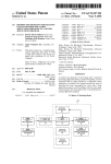
US006112016A
Ulllted States Patent [19]
[11] Patent Number:
MacWilliams et al.
[45]
[54]
6,112,016
Date of Patent:
METHOD AND APPARATUS FOR SHARING
5,551,005
A SIGNAL LINE BETWEEN AGENTS
5,568,617
*Aug. 29, 2000
8/1996 Sarangdhar et al. .................. .. 395/472
10/1996
Kametani
...................
5,572,703 11/1996 MacWilliams et al.
[75]
Inventors: Peter D_ MacWilliams,A1Oha;
5,764,935
. . . ..
395/280
395/473
6/1998 Bechtolsheim et al. .............. .. 395/325
Norman J. Rasmussen, Hillsboro, both
OTHER PUBLICATIONS
of Greg; Nicholas D. Wade,
_
Vancouver, Wash; William S_ E Wu,
cuper?no, Calif
_
_ _
_
PCI Local Bus Speci?cation, Revision 2.0; PCI Special
Interest Group; Hillsboro, OR; Apr. 1993.
Intel, :Pentium Processor User’s Manual Volume 2: 82496
'
- Intel Corporation,
'
'
[73] Assignee.
Santa Clara, Calif.
Cache Controller and 82491 SRAM Data book, 1994,
P5—114 to 5—115.
[*]
Notice:
This patent issued on a continued pros-
Primary Examiner_Glenn A Auve
ecunon aPPhFaHOP ?led under 37 CFR
Attorney, Agent, or Firm—Blakely, Sokoloff, Taylor &
1.53(d), and 1s subJect to the tWenty year
patent term provisions of 35 U.S.C.
Zafman LLP
154(a)(2)_
[57]
_
ABSTRACT
Memory bus extensions to a high speed peripheral bus are
[21] Appl' NO" 08/824’632
presented. Speci?cally, sideband signals are used to overlay
[22]
advanced mechanisms for cache attribute mapping, cache
consistency cycles, and dual processor support onto a high
speed peripheral bus. In the case of cache attribute mapping,
three cache memory attribute signals that have been sup
ported in previous processors and caches are replaced by
tWo cache attribute signals that maintain all the functionality
Filed;
Man 27, 1997
Related US, Application Data
[62]
Division of application No. 08/420,494, Apr. 12, 1995, Pat.
NO- 5,651,137
[51]
Int. c1.7 .................................................... .. G06F 13/00
of the three Original signals- In the Case Of Cache Consistency
[52]
U S C]
cycles, advanced modes of operation are presented. These
[58]
Field 0
395/287_ 395/200 62, 395/200 67
’
' 3’95/287 293
395
’
[56]
include support of fast Writes, the discarding of Write back
200 68 5003’
'
’
'
’
'
’
'
data by a cache for full cache line Writes, and read inter
vention that permits a cache to supply data in response to a
References Cited
5’230’043
llgicilginann et al' "
7/1993 Ichihasi?~
""" "
395000
memory read. In the case of dual processor support, several
neW signals and an associated protocol for support of dual
processors are presented. Speci?c support falls into three
areas: the extension of snooping to support multiple caches,
the support of shared data betWeen the tWo processors, and
the provision of a processor and upgrade arbitration protocol
7
7
5,291,529
3/1994 Crook et al.
375/109
that
_
p ermits dual p rocessors to share a sin g le g rant si g nal
5,408,636
4/1995 Santeler et al.
395/490
hne
5,418,914
5/1995
395/325
5,524,237
6/1996 Bestler et al. ........................ .. 395/550
U.S. PATENT DOCUMENTS
Heil et al. ...... ..
16 Claims, 10 Drawing Sheets
P|N# <
HEW
POUT# ‘ SBSW 7 PIN#
ORIGINAL
‘
‘
UPGRADE
PROCESSOR/CACHE
‘
'
PROCESSOR/CACHE
21_o =
>
SBO#
SDONE
SNARF#
POUT#
v
l
SH];
m
A
M
V
V
M
U.S. Patent
Aug. 29,2000
6,112,016
Sheet 1 0f 10
Km
UPGRADE
PRocEssoR
PRocEssoR
m
EXTERNAL
CACHE
m
JQQ
HIGH SPEED
PERIPHERAL BUS
140
<
I 1
BUS
BRIDGE
MAIN
MEMORY
1_50
1m
INPUT/OUTPUT
(v0) BUS
170
<
I \
PERIPHERAL
DEVICES
@
FIG.
U.S. Patent
Aug. 29, 2000
PROCESSOR
AND CACHE
COPFDGESSOR
AND CACHE
m
I
6,112,016
Sheet 2 0f 10
a
HIGH SPEED
PERIPHERAL BUS
140\
BUS
MAIN
BRIDGE
MEMORY
£59
1@
INPUT/OUTPUT
4
(I/O) BUS
170
I
PERIPHERAL
DEVICES
@
FIG. 2
U.S. Patent
Aug. 29,2000
Sheet 3 0f 10
6,112,016
A
msE.
L
wmm
<E
lo,IV/?mw>mo
v30
E52
tow: $05.
VAmw
ImmV
'
M“.mvir
U.S. Patent
Aug. 29, 2000
/00vL
O
X
-I
00A
\X02-I 0?
Sheet 4 0f 10
6,112,016
55<50455XVA-.
|L/@
vA
32965m72
@/
/
l
$52
$5l
$05 to”;
mw n?
'
A
v
in
.mvir
U.S. Patent
Aug. 29, 2000
Sheet 7 0f 10
6,112,016
FQIg|:\E
g1L| Ek
?zov
#25
$59: $32 $25
)?szE
b.uwir
U.S. Patent
Aug. 29,2000
Sheet 8 0f 10
6,112,016
A
msE.
G
AE5I
50
$53
ism: 150E.
tomw
#Im
tomw im w
nu.mvlri
U.S. Patent
Aug. 29, 2000
Sheet 9 0f 10
6,112,016
m2;
v30
tow: £05.
mzo w
imam im m
@.mvlri
6,112,016
1
2
METHOD AND APPARATUS FOR SHARING
A SIGNAL LINE BETWEEN AGENTS
By contrast, in a Write back caching scheme, the main
memory is not updated every time that a copy stored Within
the cache is modi?ed. Instead, in a Write back caching
scheme, the copy stored Within the cache may be modi?ed
This is a divisional of application Ser. No. 08/420,494,
?led Apr. 12 1995, US. Pat. No. 5,651,137.
BACKGROUND OF THE INVENTION
1. Field of the Invention
This invention relates to computer systems. More
particularly, this invention relates to memory transactions
Within a dual processor computer system.
10
2. Art Background
The heart of a personal computer system is usually a
central processing unit (CPU) that resides on a micropro
cessor chip. When a microprocessor operates at a high
speed, computer instructions and data must be supplied to
15
the microprocessor chip quickly if the speed of the micro
several times before the main memory is updated. This has
the advantage of reducing the traf?c on the bus because the
main memory is not updated as frequently. Furthermore,
because the main memory update can be deferred, it is
frequently possible to select a time When the bus is idle to
update the main memory With the modi?ed data. A disad
vantage of the Write back caching scheme is that the main
memory can contain stale data. This happens When the data
Within the cache has been modi?ed and the main memory
has yet to be updated With the modi?ed data. In multipro
cessor systems, or systems having direct memory access
devices, care must be taken to maintain cache coherency by
ensuring that stale data Within the main memory is not used
by a co-processor or direct memory access device.
processor is to be utiliZed effectively. The bus that provides
instructions for the microprocessor to execute, and that also
provides the data that the microprocessor Will use When
A cache consistency protocol is a set of rules by Which
states are assigned to cached entries (lines) in order to help
executing these instructions, can become a bottle neck in a
maintain cache consistency. The rules apply for memory
computer system having a fast microprocessor.
read and Write cycles. Every line in a cache is assigned a
state dependent on both processor generated activities and
If the next instruction to be executed is not available When
the microprocessor needs it, then the microprocessor must
Wait idly While the required instruction is retrieved and
provided to the microprocessor. This idling also occurs When
activities generated by other bus masters (e.g., snooping).
25
The MESI cache consistency protocol consists of four
states that de?ne Whether a line is valid (i.e., hit or miss),
Whether it is available in other caches, and Whether it has
been modi?ed. The four states are: M (Modi?ed), E
the microprocessor has the next instruction to be executed
available, but the next instruction to be executed requires
data that is not immediately available to the microprocessor.
In order to decrease the frequency With Which the micro
processor encounters these Wait cycles, many modern high
performance microprocessors have a small internal cache
sometimes called a primary cache. Instructions that are
(Exclusive), S (Shared) and I (Invalid). A M-state line is
available in only one cache and it is also modi?ed (i.e., it is
different from main memory). An E-state line is also avail
able in only one cache in the system, but the line is not
modi?ed (i.e., it is the same as main memory). AWrite to an
E-state line Will cause the line to become modi?ed. A line
35 With a S-state indicates that the line is potentially shared
so that they can be accessed immediately by the CPU of the
With other caches (i.e., the same line may exist in more than
microprocessor.
one cache). A Write to a shared line Will generate a Write
through cycle. The Write through cycle may invalidate this
When an instruction is to be executed or data is required,
line in other caches. Finally, an I-state indicates that the line
the cache is checked to determine Whether a copy of the
is not available in the cache. Aread to this line Will be a miss
required instruction or data is immediately available Within
and may cause a line ?ll operation (i.e., a fetch of the Whole
the cache. If a copy is stored Within the cache (called a cache
line into the cache from main memory). AWrite to an invalid
hit), then the copy can be supplied to the CPU immediately
line Will typically cause the processor to execute a Write
from the cache, and there is no need for the CPU to Wait
through cycle on the bus.
While the instruction or data is retrieved to the micropro
likely to be executed, and data that is likely to be required
by the executing instructions, are stored in the internal cache
cessor chip from Wherever it is stored Within the computer
system. On the other hand, if a copy is not stored Within the
cache (called a cache miss), then the CPU must Wait While
the instruction or data is retrieved to the microprocessor chip
from Wherever it is stored Within the computer system.
When executing a program, the CPU may modify the
copy of a line stored in the cache. In a Write through caching
scheme, the main memory is immediately updated When a
cached copy has been modi?ed. A Write through caching
scheme has the advantage that data in the cache is alWays
consistent With data in main memory. This is especially
45
Inquire cycles, also called snoop cycles, are initiated by
the system to determine if a line is present in a code or data
cache, and, if the line is present, What state the line has.
Inquire cycles are typically driven to a processor When a bus
master other than the processor initiates a read or Write bus
cycle. Inquire cycles are driven to the processor When the
bus master initiates a read to determine if the processor data
cache contains the latest information. If the snooped line is
in the processor data cache in the modi?ed state, the
55
advantageous in multiprocessor systems and in systems
having direct memory access devices because the main
memory alWays contains the most recent copy of the data. A
processor has the most recent information and must schedule
a Write back of the data. Inquire cycles are driven to the
processor When the other bus master initiates a Write to
determine if the processor code or data cache contains the
snooped line and to invalidate the line if it is present.
It is also common to implement the main memory using
DRAM, and then to supplement the DRAM based main
disadvantage of the Write through caching scheme is that it
increases the traf?c on the bus. This is because the bus is
immediately used to send the modi?ed data to the main
memory so that the main memory can be updated every time
that data in the cache is modi?ed. This is particularly
disadvantageous When a memory location is used to store
memory must be updated each time the temporary result
memory With a SRAM based external cache memory (i.e., a
second level cache memory that is external to the micro
processor chip). Because the external cache is not contained
on the microprocessor chip, it can typically be made to store
more data and instructions than can be stored by the internal
cache. Because the external cache is not located on the
data changes.
microprocessor chip, hoWever, it must supply the data and
temporary results that change frequently because the main
65
6,112,016
3
4
instructions to the microprocessor using one of the buses
that often form bottlenecks for data and instructions entering
presented. Speci?c support falls into three areas: the exten
and leaving the microprocessor chip.
A high speed microprocessor chip typically interfaces
shared data betWeen the tWo processors, and the provision of
sion of snooping to support multiple caches, the support of
With the rest of the computer system using one or tWo high
a processor and upgrade arbitration protocol that permits
dual processors to share a single grant signal line.
speed buses. The ?rst of these buses is a relatively high
speed asynchronous bus called a main memory bus. The
Other objects, features, and advantages of the present
invention Will be apparent from the accompanying draWings
second of these buses is a relatively high speed synchronous
and from the detailed description Which folloWs beloW.
bus called a local bus. High bandWidth devices such as
graphics adapter cards and fast input/output (I/O) devices
10
can be coupled directly to the local bus. Each device coupled
to the local bus, hoWever, has an associated capacitive load.
The objects, features, and advantages of the method and
apparatus of the present invention Will be apparent from the
folloWing detailed description of the invention in Which:
As the load on the local bus is increased, the maximum
operating speed for the local bus decreases and the poWer
required to drive the bus increases. Therefore, one device
coupled to the local bus can be a peripheral bus bridge from
the local bus to another bus called a high speed peripheral
BRIEF DESCRIPTION OF THE DRAWINGS
15
FIG. 1 illustrates a computer system Wherein a processor
is supplemented by an upgrade processor and Wherein
processor traffic is routed to a high speed peripheral bus;
bus (e.g., a peripheral component interconnect (PCI) bus).
FIG. 2 illustrates a computer system Wherein a processor
The bus bridge isolates the load of the devices coupled to the
high speed peripheral bus from the high speed local bus.
is supplemented by a co-processor and Wherein processor
traffic is ?ltered by a cache complex before being routed to
Another device coupled to the local bus is typically an
a high speed peripheral bus;
expansion bus bridge that couples the high performance
FIG. 3 illustrates a non-cacheable single Word read access
Wherein default cache attributes are assumed;
FIG. 4 illustrates a cacheable access Wherein the target
local bus to a loWer performance expansion bus. The loW
bandWidth components of the computer system are then
coupled to the loWer performance expansion bus.
The standard PCI speci?cation is targeted to support the
25
FIG. 5 illustrates coupling betWeen an original processor
and an upgrade processor;
FIG. 6 illustrates co-processor arbitration for a bus request
functions of an I/O bus. Ahigh speed peripheral bus, such as
the PCI bus, has adequate bandWidth to be used as a memory
bus for loW end systems (i.e., memory bus functionality can
be overlaid onto the I/O bus functionality). The trend in
from a non-bus oWner;
FIG. 7 illustrates co-processor arbitration With a bus grant
offered by a bus oWner;
FIG. 8 illustrates the insertion of Wait states until a snoop
mobile computers is toWards smaller, faster, less expensive
and lighter units. In entry level or mobile systems, part or all
of the system memory may be coupled directly to the PCI
completes;
bus. This may include read-only program modules as Well as
DRAM, both of Which must be cacheable by the processor.
The PCI cache support option provides a standard interface
35
FIG. 10 illustrates a memory read transaction Wherein the
agent), that alloWs the use of an inquiry (snooping) cache
coherency mechanism. This caching option assumes a ?at
address space (i.e., a single address has a unique destination
cache provides data.
DETAILED DESCRIPTION OF THE
INVENTION
In the folloWing description, for purposes of explanation,
45
hoWever, that the present invention may be practiced With
out these speci?c details. In other instances, Well knoWn
systems are shoWn in diagrammatic or block diagram form
in order not to obscure the present invention unnecessarily.
FIG. 1 illustrates a block diagram of a multi-processor
SUMMARY OF THE INVENTION
Memory bus extensions to a high speed peripheral bus are
presented. Speci?cally, sideband signals are used to overlay
advanced mechanisms for cache attribute mapping, cache
consistency cycles, and dual processor support onto a high
In the case of cache attribute mapping, three cache
memory attribute signals that have been supported in pre
vious processors and caches are replaced by tWo cache
attribute signals that maintain all the functionality of the
three original signals.
In the case of cache consistency cycles, advanced modes
of operation are presented. These include support of fast
Writes, the discarding of Write back data by a cache for full
cache line Writes, and read intervention that permits a cache
speci?c numbers, materials and con?gurations are set forth
in order to provide a thorough understanding of the present
invention. It Will be apparent to one skilled in the art,
bus such as set forth in the standard PCI speci?cation.
speed peripheral bus.
FIG. 9 illustrates a transaction completion before a snoop
result is indicated; and
betWeen PCI memory agent(s) and the bridge (or caching
regardless of access origin) and a single level bridge topol
ogy. This support option is optimiZed for simple, entry level
systems, rather than for maximum processor-cache-memory
performance. Thus, advanced mechanisms for cache consis
tency cycles, cache attribute mapping, and dual processor
support are all beyond the scope of a high speed peripheral
speci?es cache attributes;
55
computer system 100, Wherein processor 110 has been
supplemented by addition of upgrade processor 120. In
computer system 100, processor 110 is coupled by high
speed peripheral bus 140 to upgrade processor 120, external
cache 130, bus bridge 150 and main memory 160. Bus
bridge 150, in turn, is coupled by input/output (I/O) bus 170
to one or more peripheral devices 180. Input/output bus 170
is representative of a class of relatively sloW buses usually
used for loW bandWidth communications. Examples of
input/output bus 170 Would include buses adhering to the
industry standard architecture (ISA), extended industry stan
dard architecture (EISA) or micro channel architecture
(MCA) bus standards. High speed peripheral bus 140, on the
to supply data in response to a memory read.
65 other hand, is a high speed input/output bus upon Which
In the case of dual processor support, several neW signals
advanced memory bus operations have been overlaid, the
details of Which Will be set forth beloW. In the case of the
and an associated protocol for support of dual processors are
6,112,016
5
6
system of FIG. 1, high speed peripheral bus 140 has been
memory treadmill, thus alloWing the design to survive
enhanced in order to reduce the cost and complexity of
multiple generations of processor-memory technology.
system 100 by eliminating the need to provide a separate
memory bus Within the system. Thus, computer system 100
For a loW cost system, hoWever, it can make economical
sense to interface the CPU directly to the PCI bus (i.e., to
is an example of a loW end system Where central processor
provide an integrated CPU-PCI bridge). It is also possible to
further decouple the processor-memory treadmill using
unit (CPU) traf?c is routed directly to an enhanced high
speed peripheral bus. Because of the limited bus bandWidth
of bus 140, upgrade processor 120 is a turbo upgrade.
For one embodiment, high speed peripheral bus 140 is a
peripheral component interconnect (PCI) bus as de?ned by
larger or more efficient ?rst level or second level caches,
thereby alloWing a PCI bus to directly support future pro
the PCI standard, rev. 2.0 that has been augmented so as to
cessor generations.
The folloWing describes memory bus extensions to the
PCI bus for a range of CPU and second level cache com
provide enhanced memory capabilities. To provide a con
binations. In addition, the folloWing describes other system
10
sistent example, the folloWing description Will describe
modi?cations that can be made to overlay advanced memory
bus operations upon the PCI standard bus. It is to be
understood, hoWever, that the techniques set forth herein are
not limited solely to application to the PCI bus. Instead, high
speed peripheral bus 140 is representative of a class of high
speed input/output buses to Which advanced memory capa
bilities can be provided.
It is to be further understood that the architecture of
computer system 100 is merely representative of a Wide
class of computer system architectures in Which the present
invention can be practiced. For example, FIG. 2 illustrates a
block diagram of an alternate architecture multi-processor
computer system 200 that can bene?t by providing advanced
signals that can be used to support these upgrade and dual
15
25
memory bus operational capability to a high speed periph
In system 200, processor and cache complex 210 has been
supplemented by addition of co-processor and cache com
device and one caching device on the bus. The memory
extension to the PCI described herein extends this to support
up to tWo snooping devices (i.e., a dual processor MP or an
dard PCI signals and protocol Will only be described brie?y
herein. Hence, the emphasis of the folloWing discussion Will
be upon additional signals and protocol needed to extend the
PCI bus, or another type of high speed peripheral bus, into
plex 220. In computer system 200, processor and cache
complex 210 is coupled by high speed peripheral bus 140 to
input/output bus 170 to one or more peripheral devices 180.
The memory bus extension to the PCI bus Will ef?ciently
support the tWo con?gurations shoWn in FIGS. 1 and 2. In
fact, for one embodiment, a chipset de?ned to support the
memory bus extension Will logically Work With any one of
the tWo con?gurations. For the upgrade and dual processor
strategy, other system signals, such as FLUSH, INIT
(described beloW) are also de?ned such that they are com
patible across all con?gurations.
The PCI bus speci?cation explicitly alloWs one snooping
A-type processor) on the memory bus.
The folloWing description assumes that the reader is
familiar With the PCI bus speci?cation and therefore stan
eral bus 140.
co-processor and cache complex 220, bus bridge 150 and
main memory 160. Bus bridge 150, in turn, is coupled by
processor implementations.
35
an execution bus. The folloWing discussion is organiZed into
the sections: Cache Attributes, Bus Cycle De?nition,
In contrast to system 100 of FIG. 1, system 200 of FIG. 2 is
a higher-end system Wherein CPU traf?c is ?ltered by a
cache complex (i.e., a front side or back side second level
Upgrade Processor Support, Snoop Protocol, System Sig
nals and System Error Model.
cache), before being routed to high speed peripheral bus
CACHE ATTRIBUTES
140. In system 200, the ?ltering effect of the second level
cache on bus 140 traffic permits bus 140 to support a dual
The cache attribute functions are provided by the target of
processor multi-processor type (MP-type) of system.
an access. They are: Cache Enable, Write Back/Write
Alternately, in system 200, the ?ltering effect of the second
Through and Write Protection. The Cache Enable attribute
level cache on bus 140 traffic permits bus 140 to support an
application accelerator type (A-type) of system.
45
alloWs the current bus transaction to be de?ned as cacheable
or non-cacheable. The information is consequently used to
determine cycle length.
With the exception of the functionality provided to over
lay the advanced memory bus operational capability onto
high speed peripheral bus 140, computer system 100 of FIG.
For one embodiment, the memory bus extensions de?ned
herein support the MESI cache coherency protocol or any
proper subset of the MESI protocol. The Write Back/Write
1 and its constituent components operate in a manner that is
Well knoWn in the art. Furthermore, With the exception of the
Through attribute alloWs a cache line to be de?ned as a Write
functionality provided to overlay the advanced memory bus
back or Write through cache line. Thus, this attribute deter
operational capability onto high speed peripheral bus 140,
mines Whether a cache line is initially in the S or E state in
a MESI cache. If the attribute is a Write through, the cache
computer system 200 of FIG. 2 and its constituent compo
nents operate in a manner that is Well knoWn in the art. 55 line is alWays saved, or remains, in the Shared (S) state.
The Write Protection attribute alloWs a cache line to be
Therefore, the operation of computer systems 100 and 200
and their constituent components Will not be discussed
further except to describe hoW the operation of the compo
nents of computer systems 100 and 200 affect the function
protected cache line, the Write data Will bypass the cache and
ality provided to overlay advanced memory bus operational
capability onto high speed peripheral bus 140.
The Peripheral Component Interconnect (PCI) is a physi
Cache Enable, Write Back/Write Through and Write
de?ned as being Write protected. If the CPU Writes to a Write
be Written out to the external bus.
For one embodiment, the three cache attribute functions,
cal interconnect mechanism intended for use betWeen highly
integrated peripheral controller components and processor
memory systems. The PCI design Was developed to have a
system architecture that uses a CPU-PCI bridge component
to decouple the system I/O core design from the processor
65
Protection, are encoded in the folloWing tWo signals: KEN#
and WBT. Signals hereafter Will be generally referred to by
signal names. Particular signal names may be varied Without
departure from the scope and spirit of the present invention.
Further, signal states Will be referred to as being active or
inactive, high or loW, one or Zero, true or false, asserted or
6,112,016
7
8
deasserted, etc. Signals Which are active When loW are
agents, and that has meaning only to those agents that it
connects. The PCI speci?cation dictates that sideband sig
nals may never violate the speci?ed protocol for de?ned PCI
indicated by a suffix of “#”; i.e. XXX#. As examples of these
signal naming conventions, see Table 1 below:
signals or cause the speci?ed protocol to be violated. KEN#
and WBT are examples of sideband signals. In addition to
KEN# and WBT, several standard PCI signals are depicted
in FIG. 3. The PCI pin de?nitions are organiZed into the
TABLE 1
SIGNAL
NAMES
ELECTRICAL
NOTATION
LOGICAL
NOTATION
STATE
WBT
High
1 or true
Active
KEN#
Low
LoW
0 or false
1 or true
Inactive
Active
High
0 or false
Inactive
functional pin groups: System, Address and Data, Interface
Control, Arbitration (Bus Masters only), Error Reporting,
Interrupt (Optional), Cache Support (Optional), 64-bit Bus
Extension (Optional), and JTAG/Boundary Scan (Optional).
Furthermore, a decimal radix convention Will be used
When describing groups of signals. For example, AD(15:0)
Will refer to all 16 signals of signal group AD. Within each
group, the least signi?cant bit of the group is referred to With
15
a suf?x of “0.” In other Words, ADO Will refer to the least
signi?cant bit of the group and AD15 Will refer to the most
signi?cant bit.
transactions on PCI and is an input to every PCI device.
KEN# and WBT are used during a data phase of an access
to indicate the cacheability of the access. For one
embodiment, the default attribute for the access is non
cacheable (i.e., high for KEN# and WBT). For this
embodiment, When combined together, KEN# and WBT
have the folloWing encoded attributes:
Pertinent pins from the System, Address and Data and
Interface Control functional pin groups are depicted begin
ning With FIG. 3 (With the exception of the interface control
pin STOP#, Which Will not be discussed until FIG. 10).
Pertinent pins from the Arbitration and Cache Support
functional pin groups are depicted beginning With FIG. 5.
One signal shoWn in FIG. 3 is the signal at the PCI bus
CLK (clock) pin. CLK is de?ned by the PCI standard to be
a standard input-only signal. CLK provides timing for all
According to the PCI standard, With the exception of the PCI
reset signal (RST#) and the four PCI interrupt signals
(INTA#, INTB#, INTC# and INTD#), all other PCI signals
25
are sampled on the rising edge of CLK and all other timing
parameters are de?ned With respect to this edge. Thus, in
FIG. 3, six clock cycles are shoWn With each of the cycles
beginning at one of the rising edges 1A through 6A,
respectively, and ending on the next successive rising clock
edge. The PCI standard permits a PCI bus to operate at a
KEN#
WBT
Attributes
clock frequency of up to 66 MHZ and, in general, the
H
L
H
Non-Cacheable
minimum PCI bus clock frequency is DC (0 HZ).
H
Cacheable, Write-back
L
H
L
L
Cacheable, Write-through
Cacheable, Write protect
Also shoWn in FIG. 3 are the signals at the PCI Address
35
For alternate embodiments Wherein only a subset of the
cache attributes is to be supported, some of the signal pins
can be “strapped”. For example, for Write through cache
support, the WBT and KEN# pins can be tied together.
Similarly, for a Write back cache With no Write protection or
an active loW tri state signal oWned and driven by one and
only one agent at a time. The agent that drives an s/t/s pin
loW must drive it high for at least one clock before letting it
?oat. A neW agent cannot start driving a s/t/s signal any
Write through support required, the WBT# pin can be
strapped alWays high.
FIG. 3 is a timing diagram that illustrates the use of the
KEN# and WBT signals in a non-cacheable single read
access. Timing diagrams shoW the relationship of signi?cant
and Data pins, AD and C/BE#, and the signals at the PCI
interface control pins, FRAME#, IRDY#, TRDY# and
DEVSEL#. The AD and C/BE# signals are tri state (t/s)
signals. A Tri state signal is a bi-directional tri-state input
output pin. Each of the PCI interface control signals shoWn
in FIG. 3, hoWever, are sustained tri state (s/t/s) signals.
According to the PCI protocol, a Sustained tri state signal is
sooner than one clock after the previous oWner tri-states it.
45
signals involved in transactions. When a signal is draWn as
a solid line, it is actively being driven by the current master
or target. When a signal is draWn as a dashed line, no agent
A pull-up is required to sustain the inactive state until
another agent drives it, and must be provided by the central
resource.
is actively driving it. The signal may still be assumed to
According to the PCI standard, Addresses and Data are
multiplexed on the same pins, AD(31:0). A bus transaction
contain a stable value, hoWever, if the dashed line is at the
high rail. Tri-stated signals are indicated to have indetermi
nate values When the dashed line is betWeen the tWo rails
(e.g., AD or C/BE# lines). When a solid line becomes a
dotted line, it indicates that the signal Was actively driven
phases. The PCI address phase is the clock cycle in Which
the interface control signal FRAME# is asserted. Thus, in
and noW is tri-stated. When a solid line makes a loW to high 55
transition and then becomes a dotted line, it indicates the
signal Was actively driven high to precharge the bus, and
then tri-stated. A turn-around cycle is performed on all
signals that may be performed by more than one agent. The
turn-around cycle is used to avoid contention When one
agent stops driving a signal and another begins. This is
indicated on the timing diagrams as tWo arroWs pointing at
each other’s tail.
consists of an address phase folloWed by one or more data
FIG. 3, the address phase starts on clock 1A and ends on
clock 2A. During the address phase, AD(31:00) contain a
physical address (32 bits). For I/O this is a byte address; for
con?guration and memory it is a DWORD address. During
data phases, AD(07:00) contain the least signi?cant byte
(lsb) and AD(31:24) contain the most signi?cant byte (msb).
Write data is stable and valid When the interface control
signal IRDY# is asserted and read data is stable and valid
When the interface control signal TRDY# is asserted. Data is
only transferred during clocks W herein both IRDY# and
TRDY# are asserted. PCI supports both read and Write
The PCI standard permits PCI signals to be supplemented
by non PCI signals called sideband signals. A sideband
signal is loosely de?ned as any signal not part of the PCI
bursts. In FIG. 3, hoWever, there is only a single data phase.
speci?cation that connects tWo or more PCI compliant
phase.
The data phase of FIG. 3 begins on clock 2A and ends on
clock 5A. Clocks 3A and 4A insert Wait states in the data
6,112,016
9
10
Similarly, bus commands and byte enables are multi
pleXed on the PCI C/BE# pins. During the address phase of
a transaction, C/BE#(3:0) de?ne a bus command. During the
data phase C/BE#(3:0) are used as Byte Enables. The Byte
enables are valid for the entire data phase and determine
multi-data phase transaction is conditioned upon the line
being read being cacheable, IRDY# must be held back as
shoWn in FIG. 4 until the cache attributes are valid.
FIG. 4 illustrates a cacheable memory read line transac
tion. In FIG. 4 the transaction starts on clock 2B With an
address phase that occurs When FRAME# is asserted for the
Which byte lanes carry meaningful data. C/BE#0 applies to
byte 0 (lsb) and C/BE#3 applies to byte 3 (msb).
The PCI interface control signal FRAME # (Cycle frame)
transaction is beginning. While FRAME # is asserted, data
?rst time. The target then decodes the address and deter
mines that the cache line is cacheable. Therefore, on clock
3B, the target asserts KEN# and/or WBT accordingly. On
sampling KEN# or WBT active during the 2 clock WindoW,
the CPU then proceeds to complete the memory read line
transfers continue. When FRAME # is deasserted, the trans
operation (i. e., the cache line read).
is driven by the current master to indicate the beginning and
duration of an access. FRAME# is asserted to indicate a bus 10
action is in the ?nal data phase. Thus, in FIG. 3, FRAME#
is asserted at the beginning of the address phase at time 2A
and FRAME# is deasserted at time 5A during the sole, and
BUS CYCLE DEFINITION
15
hence ?nal, data phase.
The interface control signal IRDY# (Initiator ready) indi
cates the ability of the initiating agent (i.e., the bus master)
to complete the current data phase of the transaction. IRDY#
is used in conjunction With the interface control signal
sub-sections: command mapping, multidata phase cycle
requirements, special cycle mapping and con?guration
20
space mapping.
Command Mapping
TRDY# (Target ready). Signal TRDY# indicates ability of
the target agent (i.e., the selected device) to complete the
This sub-section speci?es hoW CPU bus commands map
into the PCI bus commands. The possible number of
DWORD transfers that the CPU Will attempt to burst in the
transaction is also presented. Because PCI supports transfers
of variable length, there is no requirement herein regarding
current data phase of the transaction. A data phase is
completed on any clock that IRDY# and TRDY# are both
sampled asserted. During a Write, IRDY# indicates that valid
data is present on AD(31:00) and TRDY# indicates the
target is prepared to accept data. During a read, TRDY#
indicates that valid data is present on AD(31::00) and
IRDY# indicates that the master is prepared to accept data.
Wait cycles are inserted until both IRDY# and TRDY# are
In this section, bus cycles relating to CPU access cycles
are de?ned. Their de?nitions and rules are described in four
hoW long a memory read or memory Write can be. Thus, for
eXample, a memory Write of three transfers (for possible
30
Write packetiZing, etc.) is not precluded.
A PCI Memory Read Line command (signi?ed by a
C/BE(3:0) value of 1110) maps to a CPU intended cacheable
asserted together.
When actively driven, the interface control signal
DEVSEL# (Device select) indicates that the driving device
code or data read access. The KEN# and WBT cache
attributes are used to qualify the PCI memory read line
has decoded its address as the target of the current access. As
35 command. Thus, the possible number of transfers that the
an input, DEVSEL# indicates Whether any device on the bus
CPU Will attempt to burst in the transaction Will be 1, 2 or
has been selected. In FIG. 3, DEVSEL# indicates on clock
4 When KEN# is inactive and WBT is active. OtherWise, the
2A or 3A that the target has decoded the address of the
address phase as being intended for it. The target then holds
DEVSEL# loW until clock 6A When the transaction has
completed.
number of transfers that the CPU Will attempt to burst Will
be 4 or 8. For all other command mappings the KEN and
40
For one embodiment shoWn in FIGS. 3 and 4, each cache
attribute takes on its default value if neither one of the KEN#
and WBT signals is asserted loW Within a tWo clock WindoW
after the ?rst clock FRAME# is asserted active. KEN# and
WBT Will be sampled as valid on the clock in Which either
one of the signals is asserted loW during the tWo clock
WBT signals do not modify the PCI command.
APCI Memory Write and Invalidate command is signi?ed
by a C/BE(3:0) value of 1111 and maps to a CPU intended
access of a cache line transfer for a Write back cycle. The
number of transfers that the CPU Will attempt to burst Will
45 be 4 or 8.
The PCI commands Interrupt acknowledge, Special
Cycle, I/0 read and I/O Write (having C/BE(3:0) values of
0000, 0001, 0010 and 0011, respectively) Will map to
WindoW (FIG. 4), or at the end of the WindoW, if neither is
asserted during the tWo clock WindoW (FIG. 3).
FIG. 3 illustrates a memory read line transaction Wherein 50 similarly named CPU intended accesses. In each case the
CPU Will only attempt a single transfer.
a CPU initiates a cache line read. In FIG. 3, the memory read
The PCI memory read command type (C/BE of 0100)
line transaction starts on Clock 2A With an address phase
maps to a non-cacheable code or data read CPU access and
that occurs When FRAME# is asserted for the ?rst time. A
the CPU Will attempt to burst transfer 1, 2 or 4 DWORDs.
cacheable central resource device has a tWo clock WindoW
ending at clock 4A to decode the address and assert KEN# 55 Similarly, the PCI memory Write command type (C/BE of
0111) maps to a non-cacheable cache Write CPU access and
and WBT accordingly to indicate a cacheable access. In FIG.
the CPU Will attempt to burst transfer 1 or 2 DWORDs.
3, KEN# and WBT remain high during the tWo clock
WindoW. Therefore, because the CPU has not been informed
The PCI con?guration read command type (C/BE of
by clock 4A (the end of the tWo clock WindoW) that the
1010) maps to a 32 bit I/O read CPU access to heX address
access is cacheable, the CPU then deasserts FRAME# to
indicate a single Word transfer.
60
As shoWn in FIG. 3, for a single data phase transfer,
FRAME# is deasserted at the same time that IRDY# is
asserted. For a multiple data phase transfer such as that of
FIG. 4, the CPU Will deassert FRAME# When starting the
0CFC. Similarly, the PCI con?guration Write command type
(C/BE of 1011) maps to a 32 bit I/O Write CPU access to heX
address 0CFC. In each case the CPU Will only attempt one
transfer.
65
Multi-Data Phase Cycle Requirements
last data phase (this requires that IRDY# is asserted). For
In the case of a read cycle, the PCI protocol alloWs the
read transactions Wherein Whether or not the transaction is a
master or the target to abort during a transaction. For a 64 bit
6,112,016
11
12
aligned read transaction (this corresponds to PLOCK bus
cycle in the standard i486 bus), the target and the CPU is
Finally, the ICE (in circuit emulation) special cycle pro
vides ICE support for a PCI based CPU-cache subsystem.
The ICE special cycle is de?ned as a handshake betWeen the
CPU and the ICE only. An additional sideband signal can
then be used to permit transactions betWeen the CPU and the
ICE.
required to guarantee an atomic transaction. The CPU Will
assert IRDY# in the ?rst clock after the address phase for an
atomic 64 bit aligned read transaction. The target may then
use this to complete the transaction in an atomic fashion.
Once KEN# and WBT are asserted to indicate a cacheable
read access, the target cannot abort the transaction. For a
Con?guration Space Mappling
The PCI speci?cation de?nes hoW softWare generates
target to abort on such access is a protocol error. In such a
case the bus master Will assert the PCI system error signal,
SERR#. In the case of a CPU, the CPU also has the option
10
cycle transactions on the PCI bus. The PCI speci?cation also
of vectoring to an internal fault handling routine.
In the case of a Write cycle, the PCI protocol alloWs the
requires a con?guration register space in each PCI compliant
master or the target to abort during a transaction. For cache
line Write back and aligned 64 bit Write transactions, the
target and the CPU should guarantee atomic transaction.
This is accomplised by establishing locks on PCI With a
read. Here, CPU cache line Write back cycle is mapped to the
Memory Write and Invalidate command of the PCI bus.
Similarly, the CPU 64 bit Write cycle is mapped to the
memory Write cycle of the PCI bus. A 64 bit Write transfer
is indicated in the PCI protocol by keeping FRAME#
asserted during the ?rst IRDY# assertion. The target may
15
device. Thus, a PCI compliant processors must implement
speci?c con?guration registers in order for a processor
connected directly to the PCI bus to deal With the PCI
con?guration space.
A PCI processor can be vieWed as containing tWo func
tions: the processor core and a bridge to PCI. The core
provides support for identi?cation mechanisms supported by
standard processors. The bridge, on the other hand, provides
support for the PCI con?guration space. The core and bridge
identi?cation mechanisms do not need to track each other.
Thus, for example, the core version may change While the
then use this to complete the transaction in an atomic
25
fashion.
con?guration cycles and hoW softWare generates PCI special
Most of the targets on the PCI bus Will handle a linear
mode encoded transaction more ef?ciently than a cacheline
bridge version number remains unchanged. Integrated
bridges can be hardWired to respond as device 0 on bus 0.
For one embodiment, the con?guration space of the
bridge portion does not need to be readable by any agent
Wrap. Therefore, a bus master should use a linear mode
except the contained processor core. Alternately, the con
encoded transaction Whenever possible.
?guration space of the bridge portion can be read by other
Special Cycle Mapping
agents. Whether or not the con?guration space of the bridge
system need be readable by agents other than the contained
A CPU Will generate single special cycles With one data
phase only. In the PCI speci?cation, a special cycle message
processor core is a design decision that depends upon the
necessary level of implementation complexity. In a multi
is encoded in a 32 bit data Word. The loWer 16 bits of the
data Word are the message number, alloWing for up to 64K
different message types. The upper 16 bits of the data Word
can be used to hold message speci?c information. The
message number can be programmable. The PCI speci?ca
35
system.
For one embodiment, the con?guration registers that are
tion has included Halt and ShutdoWn special cycles gener
ated by a CPU. The PCI protocol also de?nes special cycles
that can be used for sideband signal Wire replacement. The
folloWing are additional special cycles not set forth in the
PCI speci?cation that can also be generated by a CPU.
Three special cycles, CacheiFlush, CacheiWB and
processor implementation, hoWever, another mechanism,
possibly softWare based, may be provided to detect and
identify the number and types of processors Within the
implemented by the bridge portion include: Vendor ID,
Device ID, Command, Status, Revision ID, Class Code,
Cache line SiZe and Latency Timer. All other registers are
then read-only and return Zero values When they are read.
The Vendor ID and Device ID ?elds can both be imple
45
FlushiAck, concern caching of an internal processor cache.
Assertion of the processor FLUSH# pin causes an on-chip
processor cache to be invalidated. The INVD and WBINVD
processor instructions also cause an on-chip processor cache
to be invalidated. WBINVD causes the modi?ed lines in the
internal data cache to be Written back, and all lines in both
mented as read only registers, With the former identifying
the vendor providing the part and the latter identifying the
speci?c device provided by the vendor. In the case of the
Command ?eld, Bits 6 (i.e., Parity Enable) and 8 (i.e.,
SERR# Enable) Will typically be implemented as being
Writable. Depending upon the capability of a particular
processor, other bits of the Command ?eld may also be
Writable. Similarly, all de?ned bits (except bits 9, 10 and 11)
caches to be marked invalid. The CacheiFlush (?ush)
special cycle is driven after the INVD or WBINVD instruc
should be Writable. If appropriate, the Cache Line SiZe ?eld
should be implemented, in Which case the ?eld Will probably
tions are executed. It is used to indicate to the external
system that the internal caches Were invalidated and that 55 be a read only ?eld. The Class Code ?eld should be
implemented With the encoding for a host bridge (i.e.,
060000h). The Revision ID ?eld need only be implemented
external caches should also be invalidated. The CacheiWB
(Write back) special cycle is driven after the WBINVD
instruction is executed. It indicates that modi?ed lines in the
data cache Were Written back. When the FLUSH# pin is
asserted, all modi?ed lines in a Write back cache are Written
back and then all lines in the cache(s) are invalidated. The
as needed.
FlushiAck (?ush acknoWledge) special cycle is driven after
turbo upgrade, dual processor (DP) upgrade and application
the Write back and invalidation have been completed.
processor
UPGRADE SUPPORT
There are three types of processor upgrades. They are
Additionally the Britrace (branch trace) special cycle
alloWs external tracking of branch occurrences. Here the
address phase of the special cycle is used to carry a 32 bit
branch-target address.
65
upgrade. Considerations for the application
processor upgrade are very similar to considerations for the
dual processor upgrade. Hence, there Will be a turbo pro
cessor upgrade discussion and a dual-application processor
upgrade discussion only.
6,112,016
14
13
state. SNARF#, discussed in conjunction With FIG. 10,
In the case of a turbo upgrade, the original processor
cache pair are provided With an UP# (Upgrade Present)
alloWs a read intervention to occur When there is a snoop hit
input pin and the upgrade processor-cache pair are provided
thereby reducing overhead on the bus.
As shoWn in FIG. 5, the upgrade processor does not have
a REQ# signal. For one embodiment, the arbiter Will grant
With an UP# output pin. The UP# output pin of the upgrade
processor is connected directly to the UP# input pin of the
original processor-cache pair that is to be upgraded. When
the original processor access Whenever the bus is idle and no
the Upgrade Processor occupies the Upgrade Socket, the
UP# signal (active loW) forces the original processor to
other requests are pending. Thus, the REQ# signal of the
original processor is not required to be connected to the
arbiter, thereby providing a savings of one pin on the arbiter.
Alternately, the original processor has a REQ# signal to the
PCI bus arbiter With Which the original processor indicates
to the arbiter that the original processor desires use of the
bus. In the latter case, the original processor is also respon
tri-state all outputs and reduce poWer consumption. When
the upgrade processor is not in the Upgrade Socket, a pull up
resistor, internal to the original processor, drives UP# inac
tive and alloWs the original processor to control the proces
sor bus.
The dual-application processor upgrade case is more
complex than the case of a turbo upgrade because of
limitations set forth Within the PCI speci?cation. The PCI
speci?cation provides for an arbitration mechanism betWeen
bus masters. Each bus master communicates With the arbi
15
sible for asserting its REQ# signal on behalf of the upgrade
processor. In either case, hoWever, the original processor
shares its GNT# With the upgrade processor. An “oWner” is
de?ned as the processor Who oWns, or Will oWn, the PCI bus
When the GNT# line is asserted by the arbiter. The tWo
tration mechanism using the point-to-point bus master sig
processors arbitrate amongst themselves using pins PIN#
nals REQ# and GNT#, With every master having its oWn
and POUT#.
REQ# and GNT# signal. REQ# (Request) indicates to the
arbiter that the agent desires use of the bus. GNT# (Grant)
indicates to the agent that access to the bus by the agent has
PIN# (Processor IN) is an input signal and is alWays an
input to the processor regardless of Whether the processor is
been granted.
an original or upgrade processor. PIN# has one meaning
When the processor to Which it is input is the oWner and
The PCI speci?cation also provides for limited cache
support through the PCI input/output pins SDONE and
25
SBO#. SDONE (Snoop done) indicates the status of a snoop
its PIN# is a request line from the other processor indicating
for a current access. When deasserted, SDONE indicates
that the other processor requires access to the bus. When a
processor is not the oWner of the PCI bus, its PIN# is a grant
line from the oWner of the bus (i.e., from the other
that the result of the snoop is still pending. When asserted,
SDONE indicates that the snoop is complete. SBO# (Snoop
Backoff), on the other hand, indicates a hit to a modi?ed line
processor). PIN# of the original processor can be pulled high
When asserted. Thus, When SBO# is deasserted and SDONE
internally so as to disable the dual processor arbitration
function When a second processor is not present Within a
is asserted it indicates a CLEAN snoop result. A cacheable
PCI memory should implement both cache support pins as
inputs, to alloW the memory to Work With either Write
through or Write back caches. Thus, if cacheable memory is
another meaning When the processor to Which it is input is
not the oWner. When a processor is the oWner of the PCI bus,
35
system.
POUT# (Processor OUT) is an output signal and is alWays
an output from the processor regardless of Whether the
located on PCI, a bridge connecting a Write back cache to
PCI must implement both pins as outputs. A bridge con
processor is an original or upgrade processor. As Was the
case With PIN#, POUT# has one meaning When the proces
sor from Which it is output is the oWner and another meaning
When the processor from Which it is output is not the oWner.
When a processor is the oWner of the PCI bus, its POUT#
necting a Write through cache, hoWever, need only imple
ment one pin, SDONE.
The PCI speci?cation does not directly support dual
processors, hoWever. Therefore the PCI speci?cation does
not provide the appropriate signals to alloW the interaction
betWeen dual processors that is required When dual proces
is a grant line to the other processor indicating that it has
sors are present Within a system. The PCI speci?cation can 45
been granted access to the bus. When a processor is not the
oWner of the PCI bus, its POUT# is a request line to the
be extended to support dual processors by providing a dual
cache mode Wherein the original processor is required to
oWner of the bus (i.e., to the other processor).
drive SDONE and the upgrade (or second) processor is only
original processor. Whenever the oWner is to start an access,
permitted to monitor SDONE. Both processor, hoWever, are
alloWed to drive SBO# in this mode. In this case, rather than
being a standard input/output signal, SBO# is modi?ed to
become an s/t/s signal. Thus, because SBO# is a s/t/s signal,
the agent that asserts SBO# is required to restore it to the
deasserted state before tri-stating it.
To insure proper operation of the tWo caches and the PCI
the oWner folloWs the normal PCI protocol (i.e., once
FRAME# and IRDY# are deasserted and GNT# is asserted,
For one embodiment, after system reset, the oWner is the
the oWner may start a transaction). When a processor is not
55
protocol, arbitration and snoop support sideband signals are
also added. The arbitration support signals PIN# and POUT#
are shoWn in FIG. 5. Examples illustrating their operation
Will be presented in connection With FIGS. 6 and 7. The
PIN# and POUT# signals support arbitration betWeen an
original processor and an upgrade processor. The snooping
the oWner, the processor asserts its POUT# signal to indicate
to the oWner processor that the processor that is not the
oWner requires use of the bus. When PIN# of the processor
that is not the oWner is asserted by the oWner processor, the
oWner has granted the other processor access to the bus. The
processor that requested the bus then becomes the neW bus
oWner and the normal PCI protocol is folloWed (see FIG. 6).
To reduce arbitration latency, a bus oWner can also offer
bus oWnership to the other processor. The original bus oWner
can WithdraW its oWnership at any time, hoWever, so as long
as the other processor has not yet successfully claimed
support signals: SBSY# (snoop busy), SH# (share) and
SNARF# are also shoWn in FIG. 5. Examples illustrating
oWnership (i.e., POUT# is not asserted by the other proces
their operation Will be presented in connection With FIGS. 8,
sor and sampled active at the same time as PIN# is sampled
9 and 10. SBSY# alloWs the original processor and the
upgrade processor to have different and/or varying snoop
WindoWs. SH# alloWs a MESI cache to enter the shared
65
active, as shoWn in FIG. 7).
In summary, the oWnership of the bus changes Whenever
the PIN# and POUT# are sampled active at the same time.
6,112,016
15
16
In a system wherein both processors require use of the bus
have changed to the original processor on clock 6D. In either
case, hoWever, the original processor Will have to Wait for
continually, their PIN# and POUT# signals are asserted
continuously. OWnership Will change every time PIN# and
the bus to become idle on clock 7D before it can initiate a
POUT# is sampled active at the same time. POUT# of the
oWner is used to signal grant to the other processor. When
neW access.
Referring noW to FIG. 8, the snooping support signals Will
be described. In the PCI speci?cation, SDONE is driven by
oWnership changes, the same POUT# used to signal the
grant of oWnership becomes a request to the oWner for use
the snooping cache-CPU on the bus to indicate the avail
ability of the snoop result. In a dual or application upgrade
of the bus and PIN# becomes the grant to the requester.
FIG. 6 illustrates the handshaking betWeen an original
processor and a second processor (i.e., a dual or application
10
processor). As described earlier, after reset, the original
processor is the oWner and determines When the second
processor is given permission to use the interface. In this
?gure, the PIN# and POUT# shoWn are the signals of the
original processor and not those of the second processor. The
POUT# signal of the second processor is connected to the
processor arrangement, to indicate the availability of the
snoop result SDONE Will only be driven by the original
processor. To coordinate different or varying snoop WindoWs
betWeen the original processor and the second processor,
SBSY# is used.
SBSY# (Snoop Busy) is de?ned to be driven by the
original processor. This is illustrated in the ?gure by shoW
ing the PIN# and POUT# signals of the second processor in
parentheses underneath the respective POUT# and PIN#
signals of the original processor. Use of the PCI bus is
second processor to the original processor. It is used to
indicate Whether or not the snoop by the second processor
has been completed. If the second processor can complete
snooping in one cycle, SBSY# Will not be asserted. If the
second processor cannot complete snooping Within one
clock after the snoop starts, SBSY# is asserted. SBSY# is
then deasserted one cycle before the snoop result from the
second processor is available. For one embodiment, SBSY#
requested at clock IC by the second processor by asserting
its POUT# (Which is actually PIN# in the diagram). The
SBSY# does not ?oat When no second processor is present.
15
PIN# of the original processor, hoWever, and the PIN# signal
of the second processor is connected to the POUT# of the
is internally pulled up by the original processor to insure that
SH# (Share) is driven by either the second processor or
original processor detects this on clock 2C and asserts its 25
the original processor to indicate that there is a snoop hit to
POUT# on clock 3C. The second processor then becomes
a clean line. SH# is a s/t/s signal. Because GNT# from the
the oWner of the bus and deasserts its POUT# in clock 4C.
system arbiter is connected to both processors, to avoid SH#
Thus, once the second processor becomes the oWner, the
being driven by more than one processor at a time, SH# is
second processor performs the arbitration function to deter
driven only if the transaction is a memory read and the other
mine When the original processor should again have bus
processor is the master. On the basis of SH# and SBO#, the
access by becoming the oWner once again. In clock 4C, the
processor cache that initiates the memory read transaction
second processor starts a transaction.
can then determine the MESI state in Which the cache line
OWnership changes Whenever PIN# and POUT# are
should be. SH# is to be sampled on the ?rst clock When
sampled active together. Because the original processor
requires use of the PCI bus again, the original processor
keeps POUT# active on clock 4C. On clock 5C, the second
processor grants access back to the original processor by
35
SDONE is asserted and deasserted the folloWing clock. For
one embodiment, SH# is internally pulled up to insure it
does not ?oat When no second processor is present.
The original processor and the second processor share and
drive the SBO# line. Because only one processor should
drive the SBO# line one at a time, only the processor-cache
asserting its POUT# (i.e., PIN#). It is not required that either
processor immediately grant the other processor access to
the bus. In general, hoWever, the tWo processors Would
alternate accesses on the bus. On clock 5C, the original
that has a snoop hit to a modi?ed line should drive the SBO#
processor has become the neW oWner. The neW oWner,
line.
hoWever, has to Wait until the bus is idle before it can start
a transaction. Thus, it is not until clock 7C that the original
processor can start a transaction. It should be noted,
SDONE Will be asserted by the original processor When
its internal snooping is completed and the SBSY# from the
second processor is sampled deasserted. SDONE is then
deasserted by the original processor according to the stan
dard PCI protocol.
The PCI speci?cation de?nes SDONE and SBO# to
provide information betWeen agents that participate in the
hoWever, that the second processor could also have kept
PIN# asserted in clock 4C. In that case, the oWnership Would
have changed hands on clock 4C. The neW oWner still Would
have had to Wait until the bus Was idle before it could start
45
a neW transaction, hoWever.
cache protocol. There are three cache states that appear on
Referring noW to FIG. 7, eXamples of bus grant arbitration
are illustrated Wherein the bus grant is offered by the bus
PCI: STANDBY, CLEAN and HITM. When SDONE is
oWner to the processor that is not the bus oWner. In FIG. 7,
asserted, it indicates that the snoop has completed (i.e.,
SDONE is deasserted during the STANDBY state). When
SBO# and SDONE are both asserted, it indicates a hit to a
on clock 2D. The second processor then requests the bus on 55 modi?ed line (i.e., the HITM state). When SBO# is deas
serted and SDONE is asserted, it indicates that no cache
clock 3D. As a result of oWnership change to the second
con?ict exists and therefore the memory access can com
processor on clock 3D (i.e., because POUT# and PIN# are
plete normally (i.e., the CLEAN state).
sampled active), the second processor can initiate an access
on clock 4D. The second processor also offers the bus to the
SNARF#, an optional sideband signal de?ned to support
original processor on clock 4D and then WithdraWs the offer
read intervention, is shoWn in FIG. 10. The PCI speci?cation
speci?es a retry mechanism for a read transaction that results
on clock 5D. On clock 6D, the second processor again offers
in a snoop hit to a modi?ed line. The standard PCI retry
the bus oWnership to the original processor. Because the
mechanism incurs an overhead of tWo unnecessary memory
original processor asserts the bus request on clock 6D, the
bus oWnership changes back to the original processor. The
access transactions, hoWever, because the read access is ?rst
original processor is then able to initiate its access on clock 65 backed off, then the modi?ed line is Written back and the
read access is initiated again. The SNARF# signal is used to
7D. It should be noted that if the original processor Were to
provide a mechanism to remove this overhead.
have requested the bus on clock 5D, bus oWnership would
the original processor offers the bus to the second processor
6,112,016
17
18
Thus, SNARF# is used in conjunction With SDONE and
SBO# to indicate that the cache has the requested data and
is capable of providing it in the order requested. SNARF# is
modi?ed), instead of Writing it back, CLEAN can be sig
naled and folloWed by STANDBY. Because the hit to a
modi?ed line has been resolved, once HITM has been
removed from the bus, the memory controller can then
a s/t/s signal. SNARF# can only be asserted With HITM
continue With normal operation.
When the cache is capable of providing the modi?ed data in
the order requested. Thus, When the cache indicates HITM,
If a parity error is detected, the memory controller Will not
assert PERR# because it is not the true recipient of the data.
On a read transaction the assertion of PERR# is the respon
sibility of the master. Thus, if a parity error occurs the master
it may or may not assert SNARF#. SNARF# is deasserted
When the cache has placed data on the bus and is able to
complete a neW data phase on each PCI clock.
In the PCI speci?cation, on a snoop hit to a modi?ed line
10
in a cache, the cache Will Write the modi?ed line back to the
memory subsystem. This procedure requires three transac
tions on the bus. The PCI signal STOP# (Stop) indicates that
the current target is requesting the master to stop the current
transaction. Thus, the ?rst transaction occurs When the
must take the appropriate action (e.g., repeat the transaction,
set a status bit or do nothing.) If the entire line is transferred
to the master and the memory controller detects a parity
error, hoWever, the memory controller has a couple of
options With respect to hoW to handle the error. For one
15
master requests the data and is terminated With retry (i.e.,
STOP# asserted) because the snoop resulted in HITM. The
embodiment, the memory controller Will assert SERR#
because the data it has contains an error and any subsequent
read may provide corrupted data. Alternately, the memory
second transaction occurs When the cache Writes the modi
?ed line back to memory. The third and ?nal transaction
occurs When the master re-requests the data and completes
the transfer With the memory controller. The number of
controller can guarantee that a parity error occurs on any
transactions required to complete this transfer can be
causes a catastrophic system error, the second approach may
reduced from three to one if the memory controller and the
alloW the system to continue operation.
subsequent read of the affected line. This alloWs a subse
quent Write to the line that Will over-Write the bad data and
thereby ?x the parity error. Although the ?rst approach
cache coordinate the data transfer. This coordination is
accomplished by supporting SNARF#. A cache, hoWever, is
25
not required to assert SNARF# on all transactions it signals
HITM. For example, the cache may provide data When the
The memory controller is permitted to insert Wait states
until it is ready to complete a transfer. This feature is useful,
for example, When the previous transaction has ?lled the
Write buffer of the memory controller. Thus, the memory
controller can insert Wait states until the buffer is free and
then the transaction can continue. In this case, insertion of a
feW Wait states is more efficient than terminating the trans
burst sequence is linear or only Zero based (i.e., A2 and A1
both Zero).
When the cache can provide the modi?ed data in the
requested order, the cache asserts SNARF# the same time it
drives HITM on the bus. If the memory controller supports
action With retry and thereby causing tWo subsequent addi
tional transactions on the bus.
The diagram in FIG. 8 illustrates the timing associated
With the PCI cache protocol including the second processor
snar?ng, it does not assert STOP# (When it detects HITM),
but instead holds the transaction in Wait states.
to tri-state the AD lines on the next clock regardless of the
state of SNARF#. Thus, the cache insures at least one
sideband signals and their interaction. In the diagram a neW
signal called SRDY# is used. SRDY# is an internal signal
from the cache to the PCI interface logic. When SRDY# is
turn-around cycle betWeen the memory controller tri-stating
asserted, the cache has completed the snoop.
When the memory controller detects HITM, it is required
35
The transaction in FIG. 8 starts When an address is latched
the AD lines and When it starts driving the AD lines With the
?rst data requested. When the cache is ready to continue the
transfer, it deasserts SNARF# indicating to the memory
on clock 2E. The target then keeps TRDY# deasserted and
inserts Wait states until the snoop completes. The snoop
completes on clock 5E When SDONE is sampled asserted.
controller that valid data is present on the bus. To use
Because SBO# Was not asserted When SDONE Was asserted,
SNARF#, the cache guarantees that once SNARF# has been
deasserted the cache is able to provide neW data upon each
clock both IRDY# and TRDY# are asserted until an entire 45
the snoop result indicates CLEAN. Because the target
Waited for the snoop to complete, the transaction must be
cache line has been transferred. The cache also has to
cacheable. SDONE is driven by the original processor and
provide the data in the requested order When SNARF# is
asserted. Thus, for example, if the cache can only provide
is asserted When SRDY# is asserted and SBSY# is deas
serted. In this ?gure, SRDY# is asserted on clock 3E, but
SBSY# is not deasserted until clock 4E. Thus, in this
example, the snoop WindoW of the original processor is one
clock smaller than that of the second processor.
data in linear order and the current transaction requests the
data as cacheline Wrap, then the cache can not assert
SNARF# When HITM is signaled.
The memory controller is informed that the cache Will
provide the data to the master if SNARF# is asserted When
HITM is signaled. The memory controller Will therefore
latch and update the array With the data. If the master
terminates the transaction before the entire line is
transferred, the cache remains responsible for the entire line.
If the transaction is a memory read to a cacheable
55
location, the target Will insert Wait states until the snoop
completes. The memory controller Will access the requested
data and then start driving the requested data onto the bus.
The target Will continue to insert Wait states (i.e., TRDY#
Will be kept deasserted) until SDONE is asserted.
In FIG. 8, SH# is shoWn to be asserted on clock 4E or
clock 5E and then deasserted on clock 6E. If the read
The memory controller may discard the data that Was
transferred, because the cache is required to Write back the
entire line Whenever any data (in the cache line) is not
transaction is from the second processor, the original pro
transferred. The cache continues to signal HITM on the bus
cessor Will assert SH# as soon as its internal snoop is
and asserts its REQ# line, if it is going to Write back the
asserted by deasserting SRDY# (i.e., at clock 4E). If the read
modi?ed line. All cacheable transactions are terminated With
transaction is from the original processor, the second pro
retry by the memory controller While HITM is signaled. The
cache performs the Write back as it Would any Write back
caused by a snoop. If the cache determines to keep the
modi?ed line (by putting the line back in the cache as
cessor Will assert SH# as soon as its internal snoop is
65
asserted by deasserting SRDY# (i.e., at clock 5E). After
SDONE has been asserted, SH# Will be deasserted on the
folloWing clock.