1
Transparent Insertion of
Latency-Oblivious Logic onto FPGAs
Eddie Hung, Tim Todman, Wayne Luk
Department of Computing
Imperial College London, UK
{e.hung,timothy.todman,w.luk}@imperial.ac.uk
Abstract—We present an approach for inserting latencyoblivious functionality into pre-existing FPGA circuits transparently. To ensure transparency — that such modifications do
not affect the design’s maximum clock frequency — we insert
any additional logic post place-and-route, using only the spare
resources that were not consumed by the pre-existing circuit.
The typical challenge with adding new functionality into existing
circuits incrementally is that spare FPGA resources to host this
functionality must be located close to the input signals that it
requires, in order to minimise the impact of routing delays. In
congested designs, however, such co-location is often not possible.
We overcome this challenge by using flow techniques to pipeline
and route signals from where they originate, potentially in a
region of high resource congestion, into a region of low congestion
capable of hosting new circuitry, at the expense of latency. We
demonstrate and evaluate our approach by augmenting realistic
designs with self-monitoring circuitry, which is not sensitive to
latency. We report results on circuits operating over 200MHz
and show that our insertions have no impact on timing, are
2–4 times faster than compile-time insertion, and incur only a
small power overhead.
I. I NTRODUCTION
Field-programmable gate arrays (FPGAs) are a generalpurpose silicon technology capable of implementing almost
any digital design. This prefabricated flexibility exists by
provisioning generic logic resources (such as lookup-tables
and switched routing interconnect) that can be programmed at
implementation-time. The act of synthesising a design onto an
FPGA involves the use of Computer-Aided Design (CAD) tools
to compute a feasible programming sequence for some subset
of these resources in order to implement the requested circuit.
Modern FPGA devices, such as the latest family of devices
from Xilinx, can exceed 20 billion transistors making this CAD
problem an extremely difficult one. As a result, (i) FPGA CAD
can be time-consuming process [1], and (ii), due to the heuristic
nature of the algorithms that are employed inside these CAD
tools, the quality of the synthesised solution can be extremely
unstable. Prior work by Rubin and DeHon [2] finds that even
small perturbations to the initial conditions of the routing
algorithm in VPR5 can affect delay by 17–110%. Accordingly,
any modifications made to the circuit (i.e. when adding extra
functionality or fixing existing features) will require a new
synthesis solution to be computed — a lengthy procedure, and
one that may also return a worse solution — thereby impacting
designer productivity.
In this work, we present a solution for allowing new,
latency-oblivious, logic to be inserted into a pre-existing
design transparently without needing the entire circuit to be
recompiled. In the context of this work, a latency-oblivious
circuit contains no strict constraints on the number of clock
cycles for computing a result; one example of latency-oblivious
functionality would be to use trace-buffers to record on-chip
signal behaviour [3], given that pipelining any trace signals
will not affect their observability, whilst another example may
be watchdog functionality that invokes a circuit reset. The key
advantage that latency-oblivious circuits provide is that they
introduce an additional level of synthesis flexibility in order to
achieve transparent insertion.
We insert additional logic transparently, meaning that it
does not affect performance or functionality. To this end, we
insert post place-and-route, using only spare FPGA resources
not used by the original user circuit. By using such mutually
exclusive resources, new functionality can be added without
affecting the user design. To eliminate any impact on the criticalpath of the original design, we aggressively pipeline this new
circuitry, which is possible due to its latency-oblivious nature.
More explicitly, we make the following contributions:
• An approach for reclaiming the spare, unused, resources
on FPGAs to transparently insert new logic after circuit
implementation.
• Use of minimum-cost graph flow techniques to simultaneously pipeline-and-route all input signals required by this
logic, without impact on circuit timing.
• Experimentally validating and quantifying the overhead of
inserting self-monitoring logic into realistic circuits, showing that our techniques incur only a small power penalty.
The remainder of this paper is organised as follows: Section II
presents the background and reviews prior work, while Section III describes our transparent insertion approach in detail.
The methodology adopted in our evaluation, and the results of
our experiments, are presented in Sections IV and V. Finally,
we conclude in Section VI and outline the current limitations
and future work.
II. BACKGROUND AND R ELATED W ORK
Incremental compilation: Our techniques essentially allow
extra logic to be added to an existing FPGA design. Incremental
compilation reuses partial results from previous compilations
of similar designs to reduce implementation time for small
(additive and non-additive) changes, such as engineering change
orders (ECOs). Current FPGA implementation flows support
incremental compilation, accelerating implementation by up to
75% for small changes in large designs [4]; our unoptimised
flow matches existing CAD tools with speedups of 2–4 times
in our tests, whilst also guaranteeing the original circuit is
completely preserved.
Latency-insensitive design: In this work, we exploit the
flexibility provided by inserting latency-oblivious logic — logic
that provides additional functionality without strict constraints
on the number of clock cycles in which it must return a
result, if at all. An example of latency-oblivious logic is tracebuffers, which are used to record on-chip signal activity for
the purpose of debugging. In this example, the number of
pipelining registers that each traced signal passes through does
not affect its observability. More broadly, latency-insensitive
design [5] is a methodology to create designs that are insensitive
to communication delays between components, thus allowing
tools to implement them with as many pipelining stages as
necessary to meet performance criteria. This improved flexibility
comes at the cost of some area overhead (although modern
FPGA architectures already contain two flip-flops per lookup
table) and is unsuited to designs with poor communication
locality. Design components must adhere to a protocol to ensure
that inter-component communications can tolerate the extra
latency, or the design will no longer be correct. By contrast,
only the elements we add are latency-insensitive: the rest of
the design does not need to adhere to this design methodology.
Tabula’s extensive work over the last decade in transparent
observability and debugging (see, for example [6], [7], [8])
exploits the latency-insensitivity of observed signals in both
their programmable hardware and software implementations.
Network flow algorithms in FPGA CAD: A flow network
is characterised by a graph G(V, E), with V representing a
set of vertices and E a set of directed edges connecting two
such vertices. Each edge in this network is assigned a capacity
u ∈ N, and studies are typically conducted to understand how
flow can be transported over this network efficiently, with many
applications in operational research. A valid flow solution exists
when (i) the flow carried by each edge does not exceed its
capacity, and (ii) conservation of flow exists at all vertices —
that is, the sum of all flows entering a vertex must be equal to
the sum of all flows exiting — with two exceptions at the source
and the sink. The source node may only produce flow, whilst
the sink node may only consume flow. A single-commodity
network exists if there is only one type of flow present.
Efficient algorithms to compute the maximum integer flow
of a single-commodity supported by a network exist (while
multi-commodity maximum integer flow is known to be a
NP-complete problem), and have seen applications in FPGA
CAD. FlowMap [9] employs such a max-flow algorithm (more
specifically, to find its dual solution, the min-cut) during FPGA
technology-mapping in order to compute a mapped netlist
with the minimum logic-depth, whilst Lemieux et al. [10] use
max-flow for evaluating the routability of depopulated FPGA
switch-matrices. Optionally, each edge of the network can also
be assigned a cost-per-unit-flow c ∈ N, and given a fixed flow
target efficient algorithms also exist for computing the minimum
cost solution (for single-commodity flows). This technique
was applied by Lee et al. [11] to detailed FPGA routing. By
assigning wire delays to edge costs, and by taking advantage of
the feature that the inputs to a LUT are permutable, the authors
take a piecewise approach to find a minimum-cost (minimum
delay) routing solution for all inputs to each LUT individually,
and use Lagrangian relaxation techniques to resolve any routing
conflicts between LUTs.
Combining both min-cost and max-flow algorithms is
reference [3], where they are used to connect signals to tracebuffers during FPGA debug. This work takes advantage of
the fact that debugging signals need only be connected to
any available trace-buffer to be observable (thus, allowing
it to be treated as a single-commodity flow, unlike generic
1. Compile user-circuit
using vendor tools
as normal
2. Manually identify an
underutilised region to
host new logic
User input:
No. of pipelining hops
& maximum distances
3. Use mincost-flow to
iteratively pipeline-androute signals into region,
using only spare resources
4. Compile new logic
using vendor tools
on spare resources
5. Merge user-circuit
with new logic
6. Perform new logic
plus last-mile routing
using vendor tools
on spare resources
Use
Case (i)
For new
logic
operating
on the
same
signals
Use
Case (ii)
For new
logic
operating
on new
signals
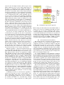
Fig. 1: Transparent logic insertion approach.
FPGA routing) and demonstrated how the maximal number of
signals can be observed for minimum wirelength. In contrast
to reference [3], we use flow techniques in this work to
concentrate signals into a single region (rather than connecting
to trace-buffers distributed across the device) in a way that does
not impact the circuit performance whatsoever. Whilst prior
work reported that adding trace-buffer connections reduced the
maximum clock frequency from 75MHz to 55MHz, we pipeline
our signal routing to mitigate all impact on performance.
III. T RANSPARENT L OGIC I NSERTION
Our general approach to inserting new logic transparent
circuitry is detailed as a six step process in Figure 1. Step 1
compiles the user-circuit as normal (for example, by using Xilinx ISE) without reserving any resources a-priori or specifying
any additional constraints over what is necessary on a regular
compilation run. Step 2 examines the floorplan of the compiled
result, and identifies an underutilised region (typically, found
at the peripheries of the device) that would support the inserted
logic. Currently, this step is manual, though we anticipate that
this can be automated in future work.
Step 3 applies minimum-cost flow techniques to transport
those user signals (which may be distributed across the whole
device) needed by the new logic circuit into the designated
region, passing through pipelining registers along the way. The
exact number of pipeline stages, and the maximum allowed
distance between each stage is currently specified by the user
— we elaborate on the full details of this step later. Crucially
though, only spare logic and routing resources that were not
consumed by the original circuit compilation are used here —
it is this characteristic which makes our approach transparent.
Based on the results from step 3, which specifies a template
containing the location of all flip-flops that were used for
pipelining, and all logic resources occupied by the user circuit,
step 4 applies vendor tools to compile (but not route) a separate
circuit implementing the new logic tailored for this template,
again using only those resources that are spare. With this new
logical circuit being mutually exclusive to the original user
circuit, step 5 then merges the pipelined-and-routed circuit
from step 3 with the newly placed circuit from step 4. Finally,
step 6 completes the unrouted connections inside the merged
circuit (which connect from the final pipelining stage to the
new circuit, and within this new circuit) using vendor tools.
For every new set of functionality
on the same set of pre
routed signals case (i) of Fig. 1 only steps 4 to 6 would need
to be repeated. However, for new
logic that operate on signals
not already routed case (ii) step 3 would also need to be
repeated in order to transport those signals.
Pipeline-and-route: A key component of this toolflow is
the ability to transport circuit signals, which may be scattered
across a device, into a concentrated region as inputs of a new
circuit, under the constraint that it may only use spare resources
that are not already occupied. Routing these signals directly
may incur large routing delays, depending on their distance.
To mitigate these large routing delays which can introduce new
critical-paths, we pipeline the signals of interest. Given that our
approach is targeted at latency-oblivious logic, these additional
pipelining stages are acceptable.
We transform the FPGA routing resource graph (with
nodes occupied by the user circuit removed) into a flow
network using similar techniques to [3] and employ minimumcost flow techniques to route all necessary signals to unique
pipelining registers from a candidate set. An important degree
of freedom that exists with this particular routing problem
(and that does not exist with user routing) is that each signal
can connect to any register from the candidate set, which
provides significant routing flexibility even under constrained
scenarios. Our approach is different from the separate placement
and routing stages employed by traditional CAD tools; in
some ways, our tool can be seen as routing signals, resolving
congestion, and placing pipelining registers simultaneously.
Furthermore, unlike reference [3], we do not seek to find
the routing solution with maximum signal observability, but
instead wish to use flow algorithms to perform both placement
and routing during signal pipelining.
Given timing estimates (costs) for each edge in the flow
network, the objective function that these techniques minimise
is the average-case timing for each connection, which is not
the same as the worst-case timing across all connections that
determines the critical-path delay. Nevertheless, we have found
in our experiments that when a user chooses the candidate
register set conservatively (through the number of pipelining
hops, and the distance of each hop from the anchor point), our
approach is capable of returning solutions that will not increase
the circuit’s critical-path delay. It is worth pointing out that we
do not apply min-cost flow techniques in search of the optimal
timing solution, for the following reasons: a) due to the nature
of the network flow problem, it is only possible to optimise for
average-case timing, b) we modify the network in a heuristic
manner to guide algorithm behaviour in ways that do not reflect
the true device, and c) the fact that, whilst each application
of min-cost flow is proven to find the global optimum, when
applying this technique iteratively (in a piecewise fashion) for
each pipeline stage, optimality is no longer guaranteed. Instead,
we prefer to consider the flow approach to be an effective
heuristic for this particular routing problem.
In our tool, the candidate set of registers is specified as spare
flip-flops that fall within a certain straight-line distance from
an (X, Y ) anchor location on the FPGA. Spare flip-flops may
be present inside slices partially occupied by the user circuit
(but care must be taken to ensure that such logic slices belong
to a compatible clock domain to the signals being transported)
or by placing new slices onto unoccupied sites. The region
determined by the anchor and radius is a circle (or a segment,
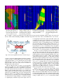
Anchor
⚓
Pipeline registers
⚓
⚓
r=30
r=40
r=50
Signals
New routing
(a) First hop
(b) Second hop
(c) Third hop
Fig. 2: Pipeline-and-route technique — by iteratively decreasing
the set of candidate registers (as outlined, specified using radius
r) from anchor point, signals are pipelined to their destination.
if cropped by the FPGA boundary). By iteratively reducing the
radius of this circle over multiple routing passes, and hence
reducing the candidate set of pipelining registers, it is possible
to migrate signals towards the anchor point, at the expense
of additional latency for each pipeline hop. This is illustrated
by Figure 2: in each iteration, signals that fall outside of the
candidate region are routed into its minimum-cost flip-flop
inside the region. Those signals that are already inside the
region are also routed to a different flip-flop inside the region,
in order to maintain latency between signals.
To guide the min-cost flow algorithm into returning a valid
routing solution, we make two heuristic modifications to our
network. Firstly, we apply a penalty to all network edges that
cross an FPGA clock region. In some devices, all resources
belong to an unique clock region, and signals that cross a
region will incur some clock skew. During our experiments,
we observe that in certain cases, the min-cost algorithm would
return extremely short routing paths that bridge across two
different regions, which combined with a positive clock skew,
resulted in a hold time violation. To discourage such paths,
we add an inflated delay penalty to all such edges. Secondly,
we also observe that it is possible for the min-cost algorithm
to connect to pipelining registers that have their output pin
blocked due to routing congestion. Given that we route signals
in a piecewise fashion, it would not possible for one min-cost
iteration to understand the routability of the following iteration.
To alleviate this issue, during candidate flip-flop selection, we
filter out all registers that do not have sufficient free fan-outs
available for downstream usage.
IV. E VALUATION METHODOLOGY: X ILINX
Although we believe that our techniques are applicable for
all FPGA vendors, we evaluate our work on Xilinx technology.
In the following evaluation, we first employ Xilinx ISE v13.3
to compile the original user circuit (step 1 from Fig. 1). For
designs supplied with timing constraints we apply those to ISE,
but for designs without we operate ISE in its ‘performance
evaluation mode’ which infers all clocks from the circuit and
minimises their clock periods. For step 2, we open the compiled
design in Xilinx’s FPGA editor in order to visualise its floorplan,
and identify an underutilised region in the device that could
host any new circuitry.
Next, step 3 involves decoding the place-and-routed netlist
returned by ISE from its proprietary binary format, NCD,
into the equivalent Xilinx Design Language format, XDL
using the command xdl -ncd2xdl. The XDL format is
(a) Step 1: Floorplan of the
place-and-routed solution for
the user circuit, with resources
from each of the en-/de-coders
shown in a different colour.
(b) Step 3: Floorplan after iteratively adding 5 waves of
pipelining registers that transport data into the top-right region (alternating green/yellow).
(c) Identical floorplan to (b),
but with rats nest for pipelining
connections highlighted (alternating green/yellow).
(d) Step 6: Final floorplan
for augmented circuit: inserted
logic is marked in white, example signal routing path shown
in cyan.
Fig. 3: Adding 3 x 128-bit monobit checks to the AES (3-pair) encoder+decoder benchmark, which occupies 92% logic slices
and 71% LUTs, whilst maintaining 237MHz. An unusable region that exists in the centre of this FPGA device is also shown.
From Step 1
Circuit Netlist
(XDL)
Re-entrant
capability
for iterative
application
From Step 2
Signals to route
(regex)
Clock Signal
Anchor point
(X,Y,radius)
Pipeline-and-Route
tool
Modified Circuit Netlist
(XDL)
To Step 5
Insertion Template
(Verilog & UCF)
To Step 4
Fig. 4: Our custom pipeline-and-route tool used in step 3.
a verbose, text-based, human-readable format that contains a
complete description of Xilinx FPGA netlists: from LUT masks,
component placements, to source and sink pins, and even which
individual wires are used to compose every routed net in the
design. Toolkits, such as Torc [12], exist for researchers to
manipulate this format with ease.
After decoding the circuit, we apply our custom pipelineand-route tool (built on top of Torc for manipulating XDL, and
employing LEMON [13] for flow computations) to execute the
procedure described in Section II. This tool is illustrated in
Figure 4: given an XDL circuit netlist, a set of signals to be
routed (which can be specified as regular expressions matched
against nets in the XDL netlist), the clock domain that they
belong in, and the set of candidate registers (specified by an
anchor point (X, Y ) and radius r) the tool will apply minimumcost network flow routing techniques to transport all signals
to a pipelining flop within this region. The output of this tool
is an augmented circuit netlist, again in the XDL format, and
a template that can be used to build the new circuit in the
following step. This template is made up of a Verilog file that
specifies the location of all pipelining registers, and a Xilinx
User Constraints File (UCF) that specifies which resources on
the device are currently occupied and cannot be used for new
logic (using the PROHIBIT constraint). Lastly, our pipelineand-route tool is re-entrant, meaning that the output netlist can
be used as the input netlist for the next routing run, allowing
this procedure to be executed iteratively for each pipeline hop.
In step 4, we take the template produced in the previous
step, add new functionality into the Verilog, and synthesise
and place (but not route) this circuit using ISE. Currently, we
require that this new circuit be manually pipelined at the source
level, although it may be possible to employ register-retiming
optimisations within the synthesis tool. The UCF constraints
file enforces mutual exclusivity between logic resources in the
user and the added circuit, and is also used to force the Xilinx
placer to utilise the host region identified in step 2 (using an
AREA_GROUP constraint). We do not route the added circuit
in this step because it is currently impractical (and perhaps,
even impossible within the Xilinx toolflow) to enforce mutual
exclusivity on routing resources. For step 5, we decode this
added circuit into XDL and then use a custom tool to merge
this into the pipeline-and-routed circuit from step 3.
Finally, in step 6 we convert the merged XDL circuit
back into the binary NCD format using the inverse command
xdl -xdl2ncd (which also invokes the Design Rule Check,
DRC) and invoke the Xilinx PAR router in its re-entrant mode
to both route the added circuit, and to complete last-mile routing
from the final pipelining stage to the new circuit’s inputs. During
routing, we employ the RCT_SIGFILE environment variable
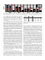
Exp. 1: LEON3 SoC
This work Resynthesis
User circuit:
Slice utilization
LUT utilization
Register utilization
Critical-path delay
Pipe-and-routed ckt:
Signals routed
Slice utilization
LUT utilization
Register utilization
Critical-path delay
Pipeline latency
Monitoring circuit:
Slice utilization
LUT utilization
Register utilization
Critical-path estimate
Monitor latency
Final circuit:
Critical-path delay
Exp. 2: AES (3 pair)
This work Resynthesis
30,698 (81%)
82,830 (54%)
60,725 (20%)
13.324ns
34,880 (92%)
108,132 (71%)
32,022 (10%)
4.213ns
Exp. 3: AES (2 pair)
This work Resynthesis
Exp. 4: FloPoCo
This work Resynthesis
26,362 (69%)
71,976 (47%)
21,391 (7%)
4.153ns
24,650 (65%)
61,967 (41%)
97,968 (32%)
6.232 ns
240
30,720 (+22)
82,925 (+95)
61,205 (+480)
13.324ns
2
-
384
34,985 (+105)
108,264 (+132)
33,942 (+1,920)
4.213ns
5
-
512
26,890 (+528)
72,216 (+240)
23,951 (+2,560)
4.153ns
5
-
144
24,790 (+140)
61,996 (+29)
98,400 (+432)
6.232ns
3
-
30,770 (+50)
83,078 (+153)
61,454 (+249)
3.729ns
3
33,642
82,489
60,973
3
35,140 (+155)
108,831 (+567)
34,636 (+694)
2.436ns
8
35,104
108,591
32,689
8
28,045 (+1155)
76,478 (+4262)
28,385 (+4434)
2.758ns
8
25,807
75,996
27,765
8
24.839 (+49)
62,163 (+167)
98.550 (+150)
3.162ns
3
23,842
63,738
98.100
3
13.324ns
13.327ns
4.213ns
4.205ns
4.153ns
4.318ns
6.232ns
10.085ns
TABLE I: Detailed comparison between our proposed method and the resynthesis approach.
Plain-text
128b LFSR
128b LFSR
Encoder key
LED
output
Encrypted-text
Encoder
Encoder
Encoder
Decoder key
(delayed)
Decoder
Decoder
Decoder
==
128b LFSR
Plain-text (delayed)
Fig. 5: User benchmark for experiment 2: AES (3-pair)
encoder+decoder block diagram.
to force PAR not to rip-up any existing nets from the user
circuit and to use only spare routing resources instead.
We target the Xilinx ML605 evaluation kit, which contains
a mid-range Virtex6 FPGA (xc6vlx240t) with 150,000 six-input
LUTs arranged into 38,000 slices spread over a grid of 162x240
logical tiles. We employ four different benchmark circuits in
this work, chosen for their complexity, variety and high clock
speeds: LEON3, a System-on-Chip design, two variants of an
AES encoder/decoder, and a floating-point datapath. On each
of these benchmarks, we insert self-monitoring circuitry in
order to verify that each circuit is functioning within its normal
operating parameters. Should the monitoring circuitry detect a
failure, an alert would be raised with the device administrator
for manual intervention. For this application, the response speed
is not critical, thus allowing the inserted logic to be latencyoblivious.
The Aeroflex Gaisler LEON3 [14] is an open-source
(VHDL) multi-core SoC design that is capable of booting
Linux. The design is parameterised to allow the number, size
and configuration of SPARC cores and on-chip peripherals to be
customised. In this work, we configure the LEON3 with 8 cores,
each with 64kB of I-cache and D-cache, and MMU, DDR3
memory controller, Ethernet and CompactFlash peripherals.
The LEON3 ML605 template constrains the main SoC clock
(one of several clocks) to 75MHz (13.33ns).
For a more datapath orientated benchmark, we construct
two variants of an 128-bit AES encoder/decoder; the block
diagram for the 3-pair variant is shown in Fig. 5. This circuit has
been derived from [15], but modified by inserting an additional
pipelining stage within each AES round to improve circuit
performance at the expense of doubling encoding and decoding
latency from 10 cycles to 20 cycles. The advantage of this
benchmark is that it is entirely self-stimulating (with both its
plain-text and encoder key inputs generated by linear-feedback
shift registers), as well as self-checking, with each encoder
paired with a decoder that allows the decoded result to be
verified against the original plain-text input (regenerated via
an offset LFSR).
Lastly, we also experiment on a floating-point datapath built
using FloPoCo [16]. We use P parallel copies of a W -tap singleprecision floating-point moving average filter. Each filter’s input
is stimulated using one 32-bit LFSR, and for a 400MHz target
frequency, FloPoCo returns a circuit with pipeline latency of 45.
To generate a medium utilisation circuit, we choose P =24 and
W =8 and disable the shift-register extraction optimisation in
the synthesis tool (which would implement shift-registers using
distributed memory) in order to create a benchmark with higher
flip-flop utilisation.
V. R ESULTS
A. Experiment 1: simple monitor for LEON3
For the first experiment, we investigate inserting a set of
simple checks into the LEON3 benchmark. As an example,
we insert a combinational monitor to check that the program
counter for each of the 8 CPU cores of the SoC lies within the
memory space mapped to the DDR3 memory controller. This
emulates a viable check to ensure that instructions are only
sourced from main memory, and never from other invalid or
potentially insecure memory spaces.
Unmodified, the LEON3 benchmark consumes 81% of all
logic slices on our FPGA, 54% of all LUT resources, and meets
the 13.33ns (75MHz) clock constraint, as listed in Table I,
column 2. After examining the circuit floorplan, we identify an
underutilised region towards the upper-left side of the device,
and specify (0,185) as the anchor point. We invoke our pipelineand-route tool twice (step 3 from Fig. 1) to transport the
necessary signals towards this anchor through two pipelining
stages, first with radius 160 and secondly with radius 80. In
total, 240 bits are routed: with a 30-bit program counter (the
(ii)
(i)
(ii)
(i)
(ii)
(i)
(i)
(ii)
Fig. 6: Runtime comparison between original user circuit compilation (User), resynthesis with new logic (Resyn), and our
approach. The runtime for use case (i) — exclusive of step 3, pipeline-and-route — and use case (ii), inclusive, are also shown.
2 least significant bits of the 32-bit address are unused and
hence optimised away by ISE) is extracted from each of the
8 cores. The resulting circuit consumes a small number of
additional logic resources (registers from both existing and
newly occupied slices, as well as LUTs used as route-throughs
to access those).
Next, we synthesise the monitoring circuit (step 4) finding
that it occupies an extra 50 slices and 153 LUTs over the
pipelined circuit. Due to the simple nature of this monitor,
the pre-routing critical-path timing estimate for the pipelined
circuit is 3.73ns (in fact, the estimated critical-path is between
the final stage of pipelined signals and the monitoring circuit),
which provides a comfortable margin for meeting the 13.33ns
circuit constraint. Upon merging and routing the monitoring
circuit with the user circuit (steps 5 and 6) we find that no new
critical-paths have been introduced, and the circuit continues
to meet timing at 13.32ns.
We compare the efficiency of our transparent logic insertion
with the traditional approach to insertion, which is to add the
monitor at the source-level and to resynthesise the whole circuit.
To ensure fairness, we manually modify the source code to
extract the signals of interest out through the circuit hierarchy,
and attach them to an identical instance of the monitor HDL.
The results of such an approach is shown in Table I under
the ‘Resynthesis’ heading. Whilst the final result shows that,
for this experiment, there is effectively no impact on timing
because both circuits continue to meet the 13.33ns constraint,
designers would still have to resynthesise their circuit for every
different set of monitors that they wish to insert. Interestingly,
these results also show a significant 10% difference between
the logic slice utilization between the original user circuit, and
the instrumented circuit; it would appear that even adding a
small amount of extra logic has caused the CAD tools to make
some very different packing decisions.
Figure 6 charts the runtime advantage of our approach. On
this particular benchmark, inserting our monitors transparently
is 3.9 times faster than resynthesising. In comparison to pipelineand-routing the monitored signals, or synthesising and placing
the monitoring circuit, runtime here is dominated by the final
routing stage using vendor tools.
B. Experiment 2: stateful monitor for AES (3-pair)
Our second experiment inserts stateful monitoring logic into
a circuit with both high maximum clock frequency and high
device utilization. The benchmark chosen for this task was the
AES circuit, with 3 pairs of encoder-decoders, as described in
Fig 5. Compiling this circuit consumes 71% of all available
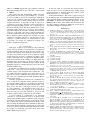
Place seed →
Benchmark ↓
AES (3x) user
AES (3x) resyn
AES (2x) user
AES (2x) resyn
FloPoCo user
FloPoCo resyn
#1
(ISE default)
4.338
4.929
4.252
4.917
6.542
9.892
#2
#3
#4
#5
4.418
4.387
4.497
4.678
9.408
6.157
4.374
4.635
4.301
4.468
9.877
9.723
4.515
4.279
4.666
5.240
6.232
10.085
4.213
4.205
4.153
4.318
9.891
10.719
TABLE II: Critical-path delay (ns) fluctuation under different
placement seeds.
LUTs on our Virtex6 device, which have been packed into 92%
of all available logic slices. The AES circuit does not contain
timing constraints, and so we operate ISE in its performance
evaluation mode to find the best timing possible, and in order
to mitigate the effect of CAD noise, we compile this circuit
using five different placement seeds (placer cost tables), the
best result returning a critical-path delay of 4.21ns, or 237MHz.
The timing for all five seeds is listed in Table II.
After examining the original circuit floorplan (shown in
Fig. 3a) we manually determine that the top-right region of
the device is underutilised, and invoke our tool five times in
order to pipeline-and-route signals into this top-right region.
We chose the top-rightmost coordinate as the anchor position
(161,239), and use decreasing radii on each iteration: 200, 160,
120, 80, 40. The signals that we picked were 128-bit buses taken
from the centre of each of the 3 encoders (more specifically,
the key_out[127:0] register from the fifth (of ten) coding
rounds), totalling 384 signals. The pipelining flip-flops that
were used are highlighted in Fig. 3b, with each iteration
alternating between yellow and green. Figure 3c augments
this by showing the (unrouted) rat’s nest corresponding to each
of our pipelined connections.
The output of a secure cryptographic function should be
uniformly distributed in order to prevent attacks — in other
words, the output should resemble that of a uniform random
number generator. A first-order test for local randomness is the
monobit test [17], which involves counting the number of ‘1’
bits in a data stream. Over a long enough sequence, it would
be expected that the number of ‘0’ bits occurring is equal to
the number of occurrences of the ‘1’ bit, within some statistical
bound. The block diagram for this monobit counter, which is
aggressively pipelined, is shown in Fig. 7. We attach three
such monitors into the AES circuit, one for each of our 128-bit
encoders, then AND these results to drive an off-chip LED.
The purpose of this monobit circuit is to count the number of
‘1’s within each 128 bit vector, and accumulate this number
128b input
32b
PopCnt
5b
+
32b
32b
PopCnt
PopCnt
5b
5b
+
6b
Input registers
(1 stage)
32b
PopCnt
+
5b
6b
Bit population counters
(2 stages)
Pipelined adder tree
(3 stages)
7b
+
rst
15b
A < input < B
Modulo 256
counter
en
1b
15 bit accumulator
(1 stage)
Range check
Output register, with enable
(1 stage)
Fig. 7: Monitoring circuit for experiment 2: 128-bit monobit
accumulator consisting of 7 pipeline stages, plus one final
reduction stage (not shown).
over 256 cycles (in total, operating on a stream of 32,768 bits).
Once this number of bits has been examined, a range check is
made to ensure that the number of ‘1’ bits lies within a certain
value: for a statistical significance p-value < 0.01, this number
is 32768
± 466. In total, the three monobit circuits consume
2
155 logic slices and 567 LUTs, and has a pre-routing timing
estimate of 2.44ns.
The final floorplan for the merged circuit is shown in Fig. 3d,
where the monitoring circuit logic resources are highlighted in
white, and all pipeline signal routing for one example signal
is shown in cyan. After routing the merged circuit, whilst
preserving all existing user nets, static timing analysis using
Xilinx’s sign-off trce tool continues to show that the criticalpath was not affected, and that the circuit continues to meet
timing at 237MHz.
A comparison against resynthesising the circuit (with monitors) from scratch shows a negligible effect (7ps improvement)
on the critical-path delay between the original and instrumented
circuits, over five placement seeds. By coincidence, the best
placement in both cases is found with a seed value of 5, but
examining the other seeds from Table II shows a significant
deviation between the two synthesis solutions: for example,
at the default seed value of 1, this timing impact exceeds
10%. The runtime improvement for the transparent approach
on this circuit is 3.0 times, and whilst the routing runtime has
decreased due to it being a less complex circuit (i.e. with only
one clock domain), we are now invoking our pipeline-and-route
tool five times.
C. Experiment 3: complex monitor for AES (2-pair)
The third experiment involves a less dense design: 2 pairs
of the AES encoder/decoder circuit, which occupies 69% of
all logic slices and 47% of all LUTs. This particular circuit
closes timing at a slightly lower period than in the previous
experiment: 4.15ns, or 241MHz.
Here, we route two 128-bit buses from each of the two
encoder blocks in this benchmark (totalling 512-bits) into the
top right region of the device, and apply a more complex pattern
counter test to each. This test involves dividing each 128-bit
value into disjoint segments each of 4-bits, and counting the
Clock speed →
User
Resynthesis
This work
Exp. 1: LEON3
75MHz
3.32W
3.32W
3.32W
Exp. 2: AES x3
66MHz
150MHz
6.00W
11.42W
6.03W
11.57W
6.09W
11.68W
Clock speed →
User
Resynthesis
This work
Exp. 3: AES x2
66MHz
200MHz
4.59W
10.36W
4.65W
10.61W
4.75W
10.88W
Exp. 4: FloPoCo
150MHz
5.69W
5.73W
5.72W
TABLE III: Measured power consumption.
number of occurrences of each 4-bit pattern. Similar to the
monobit test, over a long stream of bits, it would be expected
that each of the 24 =16 possible patterns would be equally
probable. These four pattern counters occupy 1,155 logic slices
and 4,262 LUTs.
This monitoring circuit was successfully combined with the
user-circuit without affecting its original critical-path delay of
4.15ns. Inserting the exact same monitor into the user circuit
at the source level and resynthesising degrades the critical-path
delay to 4.32ns (232MHz).
D. Experiment 4: FloPoCo monitor
The final experiment employs our FloPoCo design, which
consists of 24 parallel copies of a 8-tap moving-average
floating-point filter. With shift-register extraction disabled, the
benchmark utilises 65% of all logic slices, 41% of all LUTs,
and has a critical-path delay of 6.23ns (160MHz). The example
monitor that we demonstrate here is to check for infinity or
NaN conditions at each tap in this pipeline. The presence of
either condition is represented by FloPoCo’s internal format
by one bit going high, for all taps this totals 144 bits.
Rather than just signalling if any check had failed, we build
a priority encoder to transform the 144 bit input into an 8 bit
encoded output in order to assist a designer in locating the
failure. This monitoring circuit was also successfully added
into the user circuit without impacting the critical-path delay,
whilst resynthesis with the same placement seed degraded the
maximum frequency from 160MHz to less than 100MHz. Over
five seeds, though, the best resynthesis result was 162MHz as
shown in Table II.
E. Power evaluation
Lastly, we investigate the power implications of our circuits
with and without the monitors operating. We employ the ML605
evaluation kit’s support for on-chip power measurement (via
the Virtex6’s built-in System Monitor primitive) to return the
results in Table III, showing the power consumption for the
original user circuit without any monitoring functionality, for
monitors added at the source level where the entire circuit is
resynthesised, and lastly, for the transparent approach taken
by this paper. All power measurements were taken using
ChipScope Analyzer averaged over 128 seconds, once the die
temperature had stabilised.
For experiment 1, we booted a Linux image that supports
up to 4 cores on the SoC, and stressed each core using a gzip
instance fed from /dev/urandom. For experiments 2 and 3
based on variants of the self-stimulating AES benchmark, we
collected results at two different clock rates. Unfortunately,
the high device temperature or current caused by running
‘AES x3’ at 200MHz triggered the power regulator’s shutdown
mechanism meaning that we were only able to collect results
at 150MHz.
These results show that, unsurprisingly, adding extra monitoring circuitry does increase power consumption — on average
by 2% for resynthesis, and 4% for our techniques. Although in
some cases, the resynthesis solution is actually more efficient
(smaller area because of denser packing decisions) than the
original user circuit, our approach can still be expected to
consume more power due to the need to transport all monitored
signals, through pipelining registers, into a single region to
feed the monitoring circuit. This incurs multiple hops of extra
switching activity which does not exist for the resynthesis
approach, which has the freedom to distribute the monitoring
logic close to the signal source and not require pipelining. For
a circuit resynthesised with extra monitoring logic, however,
unless additional gating techniques are used this 2% power
overhead is permanent, whereas for our approach it is only
temporary — if self-monitoring is no longer needed, it would
be possible to recover the 4% overhead by reverting to the
original, unaugmented, bitstream.
VI. C ONCLUSION
In this paper, we have proposed a method to allow additional,
latency-oblivious circuitry to be inserted into an synthesised
circuit transparently. Our flow inserts this new circuitry only
after the user circuit has been placed-and-routed, and by using
only those resources that are spare, we do not affect the original
circuit whatsoever. In order to eliminate any impact on the
circuit’s critical-path delay, we aggressively pipeline both the
newly inserted circuit and the routing for its input signals. For
pipelining these input signals, we show how min-cost flow
techniques can be used to efficiently transport signals through
pipelining registers in a manner that places and routes those
registers simultaneously.
In summary, we find that the key benefits for transparent
insertion are: a) only spare resources are needed, even on large,
complex designs; b) the critical-path delay is unaffected, c) it is
2–3.9 times faster than resynthesis from scratch. However, our
approach does incur a small (but temporary) power overhead
due to the extra switching associated with pipelining the new
circuit’s input signals.
Currently, our transparent insertion flow is encumbered by
a set of overly-broad constraints that are necessary because we
are using the Xilinx toolflow for an unsupported application.
For example, when building the inserted circuit (step 4 of our
flow) we are only able to mark logic resources as occupied
at a slice granularity — this means that even if only one of
the four LUTs in a slice was occupied, we are prevented from
using any other part of the slice; furthermore, we are not able
to mark occupied routing resources in the same manner.
A second example is a requirement to use placement
constraints to force the inserted circuit to be placed in the
vicinity of the pipelined signals, to minimise routing congestion
between the user and inserted circuits, given that the current
flow compiles the inserted circuit without knowledge of the
leftover routing. We believe that these are limitations that can be
lifted in the future by building a special-purpose toolflow that
is tailored towards creating and inserting transparent circuits,
for example, by modifying open-source efforts such as the
VTR-to-Bitstream project [18].
In the long term, we would like the inserted latencyoblivious logic to not just read data from the existing design,
but write back into it, allowing monitoring circuits to guide
circuit behaviour or to correct faults.
ACKNOWLEDGEMENTS : This work is supported in part
by the European Union Seventh Framework Programme under
grant agreement number 257906, 287804 and 318521, by the
UK EPSRC, by the Maxeler University Programme, by the
HiPEAC NoE, by Altera, and by Xilinx. The first author would
also like to thank his colleagues at Tabula, Inc. for the support
and guidance during his internship there.
R EFERENCES
[1] K. Murray, S. Whitty, S. Liu, J. Luu, and V. Betz, “Titan: Enabling large
and complex benchmarks in academic CAD,” in 2013 International
Conference on Field Programmable Logic and Applications (FPL), Sept
2013, pp. 1–8.
[2] R. Y. Rubin and A. M. DeHon, “Timing-driven Pathfinder Pathology and
Remediation: Quantifying and Reducing Delay Noise in VPR-pathfinder,”
in Proceedings of the 19th ACM/SIGDA International Symposium on
Field Programmable Gate Arrays, ser. FPGA ’11, 2011, pp. 173–176.
[3] E. Hung, A.-S. Jamal, and S. Wilton, “Maximum Flow Algorithms for
Maximum Observability during FPGA Debug,” in 2013 International
Conference on Field-Programmable Technology (FPT), Dec 2013, pp.
20–27.
[4] Altera, “Quartus II Incremental Compilation for Hierarchical and TeamBased Design,” http://www.altera.co.uk/literature/hb/qts/qts qii51015.
pdf, June 2014.
[5] L. Carloni, K. McMillan, and A. Sangiovanni-Vincentelli, “Theory
of latency-insensitive design,” IEEE Transactions on Computer-Aided
Design of Integrated Circuits and Systems, vol. 20, no. 9, pp. 1059–1076,
Sept 2001.
[6] U.S. Patent 7,652,498.
[7] U.S. Patent 7,973,558.
[8] U.S. Patent 7,595,655.
[9] J. Cong and Y. Ding, “FlowMap: an optimal technology mapping
algorithm for delay optimization in lookup-table based FPGA designs,”
IEEE Transactions on Computer-Aided Design of Integrated Circuits
and Systems, vol. 13, no. 1, pp. 1–12, 1994.
[10] G. Lemieux, P. Leventis, and D. Lewis, “Generating highly-routable
sparse crossbars for PLDs,” in Proceedings of the 2000 ACM/SIGDA
Eighth International Symposium on Field Programmable Gate Arrays,
ser. FPGA’00, 2000, pp. 155–164.
[11] S. Lee, Y. Cheon, and M. D. F. Wong, “A Min-Cost Flow Based
Detailed Router for FPGAs,” in Proceedings of the 2003 IEEE/ACM
International Conference on Computer-Aided Design, ser. ICCAD’03,
2003, pp. 388–393.
[12] N. Steiner, A. Wood, H. Shojaei, J. Couch, P. Athanas, and M. French,
“Torc: Towards an Open-Source Tool Flow,” in Proceedings of the 19th
ACM/SIGDA International Symposium on Field-Programmable Gate
Arrays, ser. FPGA’11, February 2011, pp. 41–44.
[13] B. Dezs, A. Jüttner, and P. Kovács, “LEMON - an Open Source C++
Graph Template Library,” Electron. Notes Theor. Comput. Sci., vol. 264,
no. 5, pp. 23–45, July 2011.
[14] Aeroflex Gaisler, “GRLIB IP Core User’s Manual,” http://www.gaisler.
com/products/grlib/grip.pdf, January 2013.
[15] Altera, “Advanced Synthesis Cookbook,” http://www.altera.co.uk/
literature/manual/stx cookbook.pdf, July 2011.
[16] F. de Dinechin and B. Pasca, “Designing Custom Arithmetic Data Paths
with FloPoCo,” IEEE Design & Test of Computers, vol. 28, no. 4, pp.
18–27, 2011.
[17] L. E. Bassham III, A. L. Rukhin, J. Soto, J. R. Nechvatal, M. E.
Smid, E. B. Barker, S. D. Leigh, M. Levenson, M. Vangel, D. L.
Banks, N. A. Heckert, J. F. Dray, and S. Vo, “SP 800-22 Rev. 1a. A
Statistical Test Suite for Random and Pseudorandom Number Generators
for Cryptographic Applications,” National Institute of Standards &
Technology, United States, Tech. Rep., 2010.
[18] E. Hung, F. Eslami, and S. Wilton, “Escaping the Academic Sandbox:
Realizing VPR Circuits on Xilinx Devices,” in 2013 IEEE 21st Annual
International Symposium on Field-Programmable Custom Computing
Machines (FCCM), April 2013, pp. 45–52.