1
EP73xx User’s Guide
http://www.cirrus.com
Copyright Cirrus Logic, Inc. 2003
(All Rights Reserved)
Jan ‘04
DS508UM4
EP73xx User’s Guide Change Control Log
22 Jan 2004
Reason for entry
The Users Guide has changed from Revision 3 (UM3) to Revision 4 (UM4).
Significant Changes:
1. Typographical errors corrected.
2. Manual adapted for 90 MHz operation.
3. Crystal and PLL precision increased to 4 decimal points where applicable.
4. Distinction between 18-74 MHz (PLL) “mode” and precise “operation” frequency made. Example, at 90.3168
operating frequency the processor is in PLL, or 18-74 MHz, mode with a higher PLL Multiplier value.
5. Programming example on page 10-1 updated for consistency.
Updated Tables and Figures:
1. Revision 3, Chapter 5, ADCKSEL table on page 5-5 to 5-6 updated (Revision 4, new table is Table 5-3 on page 5-6.)
2. Revision 3, Chapter 8, Wait State tables on page 8-4 updated (Revision 4, new tables are Table 8-3 and Table 8-4 on
page 8-4.)
3. Revision 3, Chapter 9, Figure 9-2 on page 8-4, LCD Data to Pixel Mapping updated (Revision 4, new figure is Figure
9-2 on page 9-6.)
4. Revision 3, Chapter 15, Table 15-A on page 15-3, ADC Interface Operation Frequencies updated (Revision 4, new
table is Table 15-2 on page 15-3.)
5. Revision 3, Chapter 16, Table 16-A on page 16-3, Matrix for Programming the MUX updated (Revision 4, new table
is Table 16-2 on page 16-3.)
6. Revision 3, Chapter 16, Figure 16-2 on page 18-5), Digital Audio Clock Generation updated (Revision 4, new figure
is Figure 16-2 on page 16-3.)
7. Revision 3, Chapter 16, Table 16-D on page 16-5, Programmable Audio Divisors for 74 MHz updated (Revision 4,
new table is Table 16-5 on page 16-5.)
8. Revision 4, Chapter 16, Table 16-6 on page 16-6, Programmable Audio Divisors for 90 MHz added.
9. Revision 4, Chapter 17, Table 17-2 on page 17-2, UART Bit Rate at 90 MHz added.
Note: In the online version of this manual, you can click on cross-references that appear in blue text to jump
to the targeted reference.
Contacting Cirrus Logic Support
For all product questions and inquiries contact a Cirrus Logic Sales Representative.
To find the one nearest to you go to www.cirrus.com
IMPORTANT NOTICE
Cirrus Logic, Inc. and its subsidiaries ("Cirrus") believe that the information contained in this document is accurate and reliable. However, the
information is subject to change without notice and is provided "AS IS" without warranty of any kind (express or implied). Customers are advised
to obtain the latest version of relevant information to verify, before placing orders, that information being relied on is current and complete. All
products are sold subject to the terms and conditions of sale supplied at the time of order acknowledgment, including those pertaining to
warranty, patent infringement, and limitation of liability. No responsibility is assumed by Cirrus for the use of this information, including use of this
information as the basis for manufacture or sale of any items, or for infringement of patents or other rights of third parties. This document is the
property of Cirrus and by furnishing this information, Cirrus grants no license, express or implied under any patents, mask work rights,
copyrights, trademarks, trade secrets or other intellectual property rights. Cirrus owns the copyrights associated with the information contained
herein and gives consent for copies to be made of the information only for use within your organization with respect to Cirrus integrated circuits
or other products of Cirrus. This consent does not extend to other copying such as copying for general distribution, advertising or promotional
purposes, or for creating any work for resale.
CERTAIN APPLICATIONS USING SEMICONDUCTOR PRODUCTS MAY INVOLVE POTENTIAL RISKS OF DEATH, PERSONAL INJURY,
OR SEVERE PROPERTY OR ENVIRONMENTAL DAMAGE (“CRITICAL APPLICATIONS”). CIRRUS PRODUCTS ARE NOT DESIGNED,
AUTHORIZED OR WARRANTED FOR USE IN AIRCRAFT SYSTEMS, MILITARY APPLICATIONS, PRODUCTS SURGICALLY IMPLANTED
INTO THE BODY, LIFE SUPPORT PRODUCTS OR OTHER CRITICAL APPLICATIONS (INCLUDING MEDICAL DEVICES, AIRCRAFT
SYSTEMS OR COMPONENTS AND PERSONAL OR AUTOMOTIVE SAFETY OR SECURITY DEVICES). INCLUSION OF CIRRUS
PRODUCTS IN SUCH APPLICATIONS IS UNDERSTOOD TO BE FULLY AT THE CUSTOMER’S RISK AND CIRRUS DISCLAIMS AND
MAKES NO WARRANTY, EXPRESS, STATUTORY OR IMPLIED, INCLUDING THE IMPLIED WARRANTIES OF MERCHANTABILITY AND
FITNESS FOR PARTICULAR PURPOSE, WITH REGARD TO ANY CIRRUS PRODUCT THAT IS USED IN SUCH A MANNER. IF THE
CUSTOMER OR CUSTOMER’S CUSTOMER USES OR PERMITS THE USE OF CIRRUS PRODUCTS IN CRITICAL APPLICATIONS,
CUSTOMER AGREES, BY SUCH USE, TO FULLY INDEMNIFY CIRRUS, ITS OFFICERS, DIRECTORS, EMPLOYEES, DISTRIBUTORS AND
OTHER AGENTS FROM ANY AND ALL LIABILITY, INCLUDING ATTORNEYS’ FEES AND COSTS, THAT MAY RESULT FROM OR ARISE IN
CONNECTION WITH THESE USES.
Cirrus Logic, Cirrus, the Cirrus Logic logo designs, MaverickKey are trademarks of Cirrus Logic, Inc. All other brand and product names in this
document may be trademarks or service marks of their respective owners.
Microsoft Windows and Microsoft are registered trademarks of Microsoft Corporation.
LINUX is a registered trademark of Linus Torvalds.
ii
EP7309/11/12 User’s Manual - DS508UM4
Copyright Cirrus Logic, Inc. 2003
EP7309/11/12 User’s Manual - DS508UM4
Copyright Cirrus Logic, Inc. 2003
iii
1Contents
Table of Contents
Chapter 1. Introduction
Overview ............................................................................................................................................................ 1-1
Processor ..................................................................................................................................................... 1-1
Peripherals .................................................................................................................................................. 1-1
Memory Map and Register List ............................................................................................................... 1-2
Pin Description........................................................................................................................................... 1-6
Block Diagrams ............................................................................................................................................... 1-11
References ................................................................................................................................................. 1-12
Chapter 2. CPU Core
Introduction ....................................................................................................................................................... 2-1
Features .............................................................................................................................................................. 2-1
Programming Register List.............................................................................................................................. 2-1
Block Diagram ................................................................................................................................................... 2-2
Programming Examples .................................................................................................................................. 2-2
Operational Overview...................................................................................................................................... 2-4
MMU............................................................................................................................................................ 2-4
TLB ............................................................................................................................................................... 2-5
Cache ........................................................................................................................................................... 2-5
Write Buffer ................................................................................................................................................ 2-6
Debug Interface .......................................................................................................................................... 2-7
CPU Register Definitions ................................................................................................................................. 2-7
ARM720T Core Coprocessor Registers................................................................................................... 2-8
CPU Clocks ................................................................................................................................................. 2-9
PLL Multiplier Write Register (PLLW) .............................................................................................. 2-11
PLL Multiplier Read Register (PLLR)............................................................................................... 2-11
CPU State Control.................................................................................................................................... 2-12
State Control Register Descriptions ............................................................................................................. 2-13
Enter the Standby State Register (STDBY)..................................................................................... 2-13
Enter the Idle State Register (HALT) ............................................................................................... 2-14
Power Up Sequence................................................................................................................................. 2-14
RESET ........................................................................................................................................................ 2-15
Chapter 3. Timers
Introduction ....................................................................................................................................................... 3-1
Features .............................................................................................................................................................. 3-1
Timer Register List............................................................................................................................................ 3-1
Programming Example .................................................................................................................................... 3-1
Operational Overview...................................................................................................................................... 3-2
Free Running Mode................................................................................................................................... 3-2
Prescale Mode ............................................................................................................................................ 3-3
RTC Timer................................................................................................................................................... 3-3
EP7309/11/12 User’s Manual - DS508UM4
Copyright Cirrus Logic, Inc. 2003
iii
Contents
Timer Register Descriptions............................................................................................................................ 3-3
Timer Counter 1 Data Register (TC1D)..............................................................................................3-3
Timer Counter 2 Data Register(TC2D)...............................................................................................3-3
Real Time Clock Data Register (RTCDR) ..........................................................................................3-3
Real Time Clock Match Register (RTCMR)........................................................................................3-4
Chapter 4. Interrupt Controller
Introduction ....................................................................................................................................................... 4-1
Features .............................................................................................................................................................. 4-1
Interrupt Register List ...................................................................................................................................... 4-1
Programming Examples .................................................................................................................................. 4-2
Operational Overview...................................................................................................................................... 4-3
Interrupt Types and Priorities ................................................................................................................. 4-4
Interrupt Operation ................................................................................................................................... 4-4
Interrupt Listing......................................................................................................................................... 4-5
Interrupt Latencies in Different States.................................................................................................... 4-6
Interrupt Register Descriptions ...................................................................................................................... 4-8
Interrupt Status Register 1 (INTSR1) .................................................................................................4-8
Interrupt Mask Register 1 (INTMR1) ................................................................................................4-10
Interrupt Mask Register 2 (INTMR2) ................................................................................................4-12
Interrupt Status Register 3 (INTSR3) ...............................................................................................4-12
Interrupt Mask Register 3 (INTMR3) ................................................................................................4-13
Battery Low End of Interrupt (BLEOI)...............................................................................................4-13
Media Change End of Interrupt (MCEOI) .........................................................................................4-13
Tick End of Interrupt (TEOI) .............................................................................................................4-13
TC1 End of Interrupt (TC1EOI).........................................................................................................4-13
TC1 End of Interrupt (TC2EOI).........................................................................................................4-14
RTC Match End of Interrupt (RTCEOI).............................................................................................4-14
UART1 Modem Status Changed End of Interrupt (UMSEOI)...........................................................4-14
CODEC End of Interrupt (COEOI)....................................................................................................4-14
Keyboard End of Interrupt (KBDEOI) ...............................................................................................4-14
SSI2 FIFO Overflow End of Interrupt (SRXEOF) .............................................................................4-14
Chapter 5. System Registers
Introduction ....................................................................................................................................................... 5-1
Features .............................................................................................................................................................. 5-1
System Register List ......................................................................................................................................... 5-2
Programming Example .................................................................................................................................... 5-2
Operational Overview...................................................................................................................................... 5-3
Buzzer.......................................................................................................................................................... 5-3
Debug Mode ............................................................................................................................................... 5-3
System Control Register Descriptions ........................................................................................................... 5-4
System Control Register 1 (SYSCON1) .............................................................................................5-4
System Control Register 2 (SYSCON2) .............................................................................................5-7
System Control Register 3 (SYSCON3) .............................................................................................5-8
System Flag Register 1 (SYSFLG1)...................................................................................................5-9
System Flag Register 2 (SYSFLG2).................................................................................................5-12
Clear all Start-up Reason Flag Register (STFCLR) .........................................................................5-13
32-bit Unique ID Register (UNIQID) .................................................................................................5-13
Random ID 0 Register, bits 31-0 (RANDID0) ...................................................................................5-13
Random ID 1 Register, bits 63-32 (RANDID1).................................................................................5-13
Random ID 2 Register, bits 95-64 (RANDID2).................................................................................5-13
Random ID 3 Register, bits 127-96 (RANDID3)...............................................................................5-13
iv
Copyright Cirrus Logic, Inc. 2003
EP7309/11/12 User’s Manual - DS508UM4
Contents
Chapter 6. Processor Support
Introduction ....................................................................................................................................................... 6-1
Features .............................................................................................................................................................. 6-1
Operational Overview...................................................................................................................................... 6-1
Internal Boot Mode .................................................................................................................................... 6-2
External Boot Mode ................................................................................................................................... 6-2
Endianess .................................................................................................................................................... 6-4
Chapter 7. SDRAM Controller
Introduction ....................................................................................................................................................... 7-1
Features .............................................................................................................................................................. 7-1
SDRAM Register List........................................................................................................................................ 7-1
Programming Example .................................................................................................................................... 7-2
Operational Overview...................................................................................................................................... 7-2
System Initialization .................................................................................................................................. 7-2
Byte Masks .................................................................................................................................................. 7-3
SDRAM Register Descriptions ........................................................................................................................ 7-3
SDRAM Control Register (SDCONF) ................................................................................................ 7-3
SDRAM Refresh Period Register (SDRFPR) .................................................................................... 7-4
Chapter 8. SRAM/Expansion Bus Controller
Introduction ....................................................................................................................................................... 8-1
Features .............................................................................................................................................................. 8-1
SRAM / Expansion Bus Register List ............................................................................................................ 8-1
Programming Example .................................................................................................................................... 8-1
Operational Overview...................................................................................................................................... 8-2
SRAM / Expansion Bus Register Descriptions ............................................................................................ 8-3
Memory Configuration Register 1 (MEMCFG1)................................................................................. 8-3
Memory Configuration Register 2 (MEMCFG2)................................................................................. 8-5
Chapter 9. LCD Interface
Introduction ....................................................................................................................................................... 9-1
Features .............................................................................................................................................................. 9-1
LCD Register List .............................................................................................................................................. 9-1
Programming Example .................................................................................................................................... 9-2
Operational Overview...................................................................................................................................... 9-2
LCD Controller External Memory........................................................................................................... 9-2
LCD DMA Controller................................................................................................................................ 9-3
Gray Scale ................................................................................................................................................... 9-4
Hardware Interface.................................................................................................................................... 9-6
Color LCDs ................................................................................................................................................. 9-6
LCD Register Descriptions .............................................................................................................................. 9-7
LCD Control Register (LCDCON) ...................................................................................................... 9-7
LCD Palette Registers ....................................................................................................................... 9-8
LCD Frame Buffer Start Address (FBADDR)..................................................................................... 9-9
Chapter 10. Keyboard Interface
Introduction ..................................................................................................................................................... 10-1
Features ............................................................................................................................................................ 10-1
Register List ..................................................................................................................................................... 10-1
Programming Example .................................................................................................................................. 10-1
Operational Overview.................................................................................................................................... 10-2
Keyboard Interrupt Matrix..................................................................................................................... 10-2
EP7309/11/12 User’s Manual - DS508UM4
Copyright Cirrus Logic, Inc. 2003
v
Contents
Chapter 11. General Purpose I/O (GPIO)
Introduction ..................................................................................................................................................... 11-1
Features ............................................................................................................................................................ 11-1
General Purpose I/O (GPIO) Register List ................................................................................................. 11-1
Programming Example .................................................................................................................................. 11-2
Operational Overview.................................................................................................................................... 11-2
Register Descriptions ..................................................................................................................................... 11-2
Chapter 12. PWM Interface
Introduction ..................................................................................................................................................... 12-1
Features ............................................................................................................................................................ 12-1
Block Diagram ................................................................................................................................................. 12-1
PWM (Pulse Width Modulator) Register List ............................................................................................ 12-2
Programming Example .................................................................................................................................. 12-2
Operational Overview.................................................................................................................................... 12-2
PWM Register Descriptions .......................................................................................................................... 12-3
Pump Control Register (PMPCON) ..................................................................................................12-3
Chapter 13. Dedicated LED Flasher
Introduction ..................................................................................................................................................... 13-1
LED Flasher Register List .............................................................................................................................. 13-1
Programming Example .................................................................................................................................. 13-1
Operational Overview.................................................................................................................................... 13-1
Register Definitions ........................................................................................................................................ 13-2
LED Flasher Register (LEDFLSH)....................................................................................................13-2
Chapter 14. JTAG Interface
Introduction ..................................................................................................................................................... 14-1
Features ............................................................................................................................................................ 14-1
Operational Overview.................................................................................................................................... 14-1
Boundary Scan ......................................................................................................................................... 14-2
Debug Modes ........................................................................................................................................... 14-3
Software Selectable Test Functionality ................................................................................................. 14-4
Chapter 15. SSI Port
Introduction ..................................................................................................................................................... 15-1
Features ............................................................................................................................................................ 15-1
SSI Port Register List ...................................................................................................................................... 15-1
Programming Example .................................................................................................................................. 15-1
Operational Overview.................................................................................................................................... 15-2
SSI1/ADC Interface................................................................................................................................. 15-2
SSI Port Register Descriptions ...................................................................................................................... 15-4
Synchronous Serial ADC Interface Data Register (SYNCIO)...........................................................15-4
Chapter 16. DAI/CODEC/SSI2
Introduction ..................................................................................................................................................... 16-1
Features ............................................................................................................................................................ 16-1
Block Diagram ................................................................................................................................................. 16-2
DAI/CODEC/SSI2 Register List.................................................................................................................. 16-2
Programming Example .................................................................................................................................. 16-2
vi
Copyright Cirrus Logic, Inc. 2003
EP7309/11/12 User’s Manual - DS508UM4
Contents
Operational Overview.................................................................................................................................... 16-3
DAI/CODEC/SSI2 MUX ....................................................................................................................... 16-3
DAI Interface ............................................................................................................................................ 16-4
Master/Slave SSI2 Interface ................................................................................................................... 16-7
CODEC Sound Interface ....................................................................................................................... 16-10
DAI/CODEC/SSI2 Register Descriptions ................................................................................................ 16-11
DAI Mode Control Register (DAI64FS).......................................................................................... 16-11
DAI Control Register (DAIR).......................................................................................................... 16-12
DAI Data Register 0 (DAIDR0) ...................................................................................................... 16-14
DAI Data Register 1 (DAIDR1) ...................................................................................................... 16-15
DAI Status Register (DAISR)......................................................................................................... 16-16
Synchronous Serial Interface 2 Data Register (SS2DR) ............................................................... 16-20
Synchronous Serial Interface 2 Pop Residual Byte (SS2POP) ..................................................... 16-20
CODEC Interface Data Register (CODR)...................................................................................... 16-20
Chapter 17. UART and SIR Encoder
Introduction ..................................................................................................................................................... 17-1
Features ............................................................................................................................................................ 17-1
UART and SIR Encoder Register List .......................................................................................................... 17-1
Programming Example .................................................................................................................................. 17-1
Operational Overview.................................................................................................................................... 17-2
UART1 ....................................................................................................................................................... 17-3
SIR Encoder .............................................................................................................................................. 17-4
UART2 ....................................................................................................................................................... 17-4
UART and SIR Encoder Register Descriptions........................................................................................... 17-5
UART Data Registers (UARTDR1 and UARTDR2)......................................................................... 17-5
Bit Rate and Line Control Registers (UBRLCR1 and UBRLCR2) ................................................... 17-6
Appendix A. Boot Code
Index ................................................................................................................................................................... 1-1
EP7309/11/12 User’s Manual - DS508UM4
Copyright Cirrus Logic, Inc. 2003
vii
Contents
This page intentionally blank.
viii
Copyright Cirrus Logic, Inc. 2003
EP7309/11/12 User’s Manual - DS508UM4
List of Figures
Figure 1-1. EP73xx Block Diagram ............................................................................................................... 1-11
Figure 1-2. Typical EP73xx System Block Diagram ................................................................................... 1-12
Figure 2-1. ARM720T Block Diagram ............................................................................................................ 2-2
Figure 2-2. ARM720T Cache Organization ................................................................................................... 2-6
Figure 2-3. Register Organization Summary ................................................................................................ 2-8
Figure 2-4. State Diagram .............................................................................................................................. 2-12
Figure 9-1. Pixel Gray Scale Mapping............................................................................................................ 9-5
Figure 9-2. LCD Data to Pixel Mapping ........................................................................................................ 9-6
Figure 12-1. Block Diagram of a Power Supply Using Two PWM Drives ............................................. 12-1
Figure 16-1. Portion of the EP73xx Block Diagram Showing Multiplexed Feature .............................. 16-2
Figure 16-2. Digital Audio Clock Generation ............................................................................................. 16-5
Figure 16-3. SSI2 Port Directions in Slave and Master Mode ................................................................... 16-8
Figure 16-4. Residual Byte Reading.............................................................................................................. 16-9
EP7309/11/12 User’s Manual - DS508UM4
Copyright Cirrus Logic, Inc. 2003
ix
This page intentionally blank.
x
EP7309/11/12 User’s Manual - DS508UM4
Copyright 2001, 2002 Cirrus Logic
List of Tables
Table 1-1: EP73xx Memory Map in External Boot Mode ............................................................................ 1-2
Table 1-2: EP73xx Internal Registers (Little Endian Mode) ........................................................................ 1-4
Table 1-3: EP73xx Internal Registers (Big Endian Mode)............................................................................ 1-6
Table 1-4: External Signal Functions .............................................................................................................. 1-7
Table 1-5: SSI/CODEC/DAI Pin Multiplexing .......................................................................................... 1-10
Table 1-6: Output Bi-Directional Pins .......................................................................................................... 1-10
Table 2-1: Programming Registers ................................................................................................................. 2-1
Table 2-2: ARM720T Core Coprocessor Registers........................................................................................ 2-9
Table 2-3: Status of Peripherals and Clocks by Operating State .............................................................. 2-14
Table 3-1: Timer Registers................................................................................................................................ 3-1
Table 4-1: Interrupt Registers .......................................................................................................................... 4-1
Table 4-2: Vector Addresses by Interrupt Type............................................................................................ 4-3
Table 4-3: Exception Priority Handling ......................................................................................................... 4-4
Table 4-4: Interrupt Allocation in the First Interrupt Register ................................................................... 4-5
Table 4-5: Interrupt Allocation in the Second Interrupt Register .............................................................. 4-5
Table 4-6: Interrupt Allocation in the Third Interrupt Register ................................................................. 4-5
Table 4-7: External Interrupt Sources............................................................................................................. 4-7
Table 5-1: System Registers ............................................................................................................................. 5-2
Table 5-2: Keyboard Column Drive State...................................................................................................... 5-4
Table 5-3: ADC Sample Clock Settings .......................................................................................................... 5-6
Table 5-4: ARM720T Clock Speed Settings ................................................................................................... 5-9
Table 5-5: Default (Power-on Reset) Bus Width Settings .......................................................................... 5-11
Table 6-1: Chip Select Address Ranges for On-Chip Boot ROM ............................................................... 6-2
Table 6-2: Boot Options .................................................................................................................................... 6-2
Table 6-3: Memory Map in External Boot Mode .......................................................................................... 6-3
Table 6-4: Effect of Endianess on Read Operations...................................................................................... 6-4
Table 6-5: Effect on Endianess on Write Operations.................................................................................... 6-4
Table 7-1: SDRAM Registers ........................................................................................................................... 7-1
Table 8-1: SRAM / Expansion Bus Registers ................................................................................................ 8-1
Table 8-2: Bus Width Selection Settings......................................................................................................... 8-3
Table 8-3: Wait States at 13 / 18 MHz Operation......................................................................................... 8-4
Table 8-4: Wait States at 36 MHz Operation ................................................................................................. 8-4
Table 9-1: LCD Registers .................................................................................................................................. 9-1
Table 9-2: Gray Scale Value to Color Mapping ............................................................................................ 9-9
Table 11-1: General Purpose I/O (GPIO) Registers ................................................................................... 11-1
Table 12-1: PWM (Pulse Width Modulator) Registers .............................................................................. 12-2
Table 12-2: PWM Pump Drive Settings ....................................................................................................... 12-3
Table 13-1: LED Flasher Registers ................................................................................................................ 13-1
Table 14-1: Instructions Supported in JTAG Mode.................................................................................... 14-2
Table 14-2: EP73xx Hardware Test Modes.................................................................................................. 14-3
Table 14-3: Oscillator and PLL Test Mode Signals..................................................................................... 14-4
Table 14-4: Software Selectable Test Functionality .................................................................................... 14-4
Table 15-1: SSI Port Registers ........................................................................................................................ 15-1
Table 15-2: ADC Interface Operation Frequencies..................................................................................... 15-3
Table 16-1: DAI/CODEC/SSI2 Registers .................................................................................................... 16-2
Table 16-2: Matrix for Programming the MUX........................................................................................... 16-3
Table 16-3: Pin Sharing for Multiplexor....................................................................................................... 16-4
Table 16-4: Communication Interface Performance................................................................................... 16-4
Table 16-5: Programmable Audio Divisors at 74 MHz ............................................................................. 16-5
EP7309/11/12 User’s Manual - DS508UM4
Copyright Cirrus Logic, Inc. 2003
xi
Table 16-6: Programmable Audio Divisors at 90 MHz ............................................................................. 16-6
Table 17-1: UART and SIR Encoder Registers ............................................................................................ 17-1
Table 17-2: UART Bit Rates at 90 MHz ........................................................................................................ 17-2
Table 17-3: UART Bit Rate in PLL Clock Mode (74 MHz) ........................................................................ 17-3
Table 17-4: UART Bit Rate from 13 MHz Clock ......................................................................................... 17-3
Table 17-5: Word Length Selection ............................................................................................................... 17-6
EP7309/11/12 User’s Manual - DS508UM4
Copyright Cirrus Logic, Inc. 2003
xii
EP7309/11/12 User’s Manual - DS508UM4
Copyright Cirrus Logic, Inc. 2003
xiii
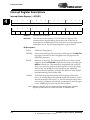
1Introduction
11
Chapter 1
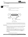
1
Overview
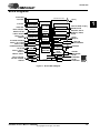
This chapter describes the EP73xx ARM processor, memory map, registers, and
signals. See the data sheet that is associated with a specific EP73xx device for more
information about pin assignments for that product.
Processor
The EP73xx incorporates an ARM 32-bit RISC micro controller that controls a wide
range of on-chip peripherals. The ARM720T includes a a 8 Kbytes unified cache and a
MMU compatible with operating systems like Windows® CE and Linux®.
See the ARM720T Technical Reference Manual, as cited on page 1-12.
Peripherals
On-chip EP73xx peripherals are product-specific for each chip. The superset of
available features includes:
• 48 Kbytes of on-chip SRAM that can be shared between the LCD controller
and general application use
• Memory interfaces (chip selects) for up to six independent 256 Mbyte
expansion segments with programmable width and wait states
• 27 general purpose Input/Outputs.
• Digital Audio Interface (DAI) to interface with CD-quality DACs and
CODECs
• Interrupt Controller
• Advanced system state controller and power management
• Two full-duplex 16550 A compatible UARTs with 16-byte transmit and
receive FIFOs.
• IrDA SIR protocol controller capable of speeds up to 115.2 kbps
• Programmable LCD controller for 1,2 or 4-bit-per-pixel with 16-level
grayscaler and frame buffer start address.
• On-chip boot ROM programmed for serial port download of boot code.
EP7309/11/12 User’s Manual - DS508UM4
Copyright Cirrus Logic, Inc. 2003
1-1
Introduction
• Two 16-bit general purpose timer counters
• 32-bit RTC (Real-Time-Clock) timer and comparator
• Dedicated LED flasher pin driven from the RTC with programmable duty
ratio (Multiplexed with GPIO pin)
1
• Two synchronous serial interfaces for Micro-wire or SPI interfaces such as
ADCs, one supporting both the master and slave and other supporting
only master mode.
• Two programmable PWM (Pulse Width Modulation) interfaces
• SDRAM interface for direct interface to a maximum of two external banks
of SDRAM memory. Each bank can be up to 256 Mbit in size and
configurable for 32 or 16-bit wide accesses.
• PLL (Phase Lock Loop) oscillator for generating core speeds of 18-90 MHz
from an external 3.6864 MHz crystal.
• Low power 32.768 kHz RTC (Real Time Clock)
• MaverickKey - Unique and Random IDs for SDMI compliance
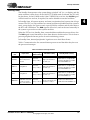
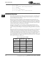
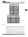
Memory Map and Register List
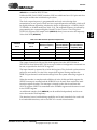
The lower 2 GByte of the address space is allocated to memory. The 64 MByte of
address space from 0xC000.0000 to 0xCFFF.FFFF is allocated to SDRAM. About
1.5 GBytes of address space, less 8 Kbytes for internal registers, is not accessible in the
EP73xx. The MMU in the EP73xx should be programmed to generate an abort
exception for access to this area.
Internal peripherals are addressed through a set of internal memory locations from
hex address 0x8000.0000 to 0x8000.3FFF. These are known as the internal registers in
the EP73xx. In Table 1-1 also shows how the 4-Gbyte address range of the ARM720T
processor (as configured within this chip) is mapped in the EP73xx. The external boot
ROM is not fully decoded (i.e., the boot code will repeat within the 256-Mbyte space
from 0x7000.0000 to 0x8000.0000). See Table 6-1 on page 6-2 for the memory map
when booted from on-chip boot ROM. The SRAM is fully decoded up to a maximum
size of 48 Kbytes. Access to any location above this range will be wrapped to within
the range.
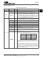
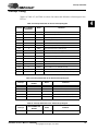
Global Memory Map
Table 1-1: EP73xx Memory Map in External Boot Mode
1-2
Address
Contents
Size
0xF000.0000
Reserved
256 Mbytes
0xE000.0000
Reserved
256 Mbytes
0xD000.0000
Reserved
256 Mbytes
0xC000.0000
SDRAM
64 Mbytes
Copyright Cirrus Logic, Inc. 2003
EP7309/11/12 User’s Manual - DS508UM4
Introduction
11
Table 1-1: EP73xx Memory Map in External Boot Mode (Continued)
Address
Contents
Size
0x8000.4000
Unused
~1 Gbyte
0x8000.0000
Internal registers
8 Kbytes
0x7000.0000
Boot ROM (nCS[7])
128 bytes
0x6000.0000
SRAM (nCS[6])
48 Kbytes
0x5000.0000
Expansion (nCS[5])
256 Mbytes
0x4000.0000
Expansion (nCS[4])
256 Mbytes
0x3000.0000
Expansion (nCS[3])
256 Mbytes
0x2000.0000
Expansion (nCS[2])
256 Mbytes
0x1000.0000
ROM Bank 1 (nCS[1])
256 Mbytes
0x0000.0000
ROM Bank 0 (nCS[0])
256 Mbytes
1
Internal Register Map
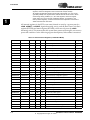
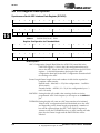
Table 1-2 on page 1-4 shows the Internal Registers of the EP73xx when the CPU is
configured to a little endian memory system. Table 1-3 on page 1-6 shows the
differences that occur when the CPU is configured to a big endian memory system for
byte-wide access to Ports A, B, and D. All the internal registers are inherently little
endian (i.e., the least significant byte is attached to bits 7 to 0 of the data bus). Hence,
the system Endianness affects the addresses required for byte accesses to the internal
registers, resulting in a reversal of the byte address required to read/write a
particular byte within a register.
There is no effect on the register addresses for word accesses. Bits A[0-1] of the
internal address bus are only decoded for Ports A, B, and D (to allow read/write to
individual ports). For all other registers, bits A[0-1] are not decoded, so that byte reads
will return the whole register contents onto the EP73xx’s internal bus, from where the
appropriate byte (according to the endianness) will be read by the CPU. To avoid the
additional complexity, it is preferable to perform all internal register accesses as word
operations, except for ports A to D which are explicitly designed to operate with byte
accesses, as well as with word accesses.
An 8 Kbytes segment of memory in the range 0x8000.0000 to 0x8000.3FFF is reserved
for internal use in the EP73xx. Accesses in this range will not cause any external bus
activity unless debug mode is enabled. Writes to bits that are not explicitly defined in
the internal area are legal and will have no effect. Reads from bits not explicitly
defined in the internal area are legal but will read undefined values. All the internal
addresses should only be accessed as 32-bit words and are always on a word
boundary, except for the GPIO port registers, which can be accessed as bytes. Address
bits in the range A[0-5] are not decoded (except for Ports A–D), this means each
internal register is valid for 64 bytes (i.e., the SYSFLG1 register appears at locations
0x8000.0140 to 0x8000.017C). There are some gaps in the register map for backward
compatibility reasons, but registers located next to a gap are still only decoded for
64 bytes.
The GPIO port registers are byte-wide and can be accessed as a word but not as a halfword. These registers additionally decode A[0-1]. All addresses are in hexadecimal
notation.
EP7309/11/12 User’s Manual - DS508UM4
Copyright Cirrus Logic, Inc. 2003
1-3
Introduction
Note: All byte-wide registers should be accessed as words (except Port A to Port D
registers, which are designed to work in both word and byte modes).
All registers bit alignment starts from the LSB of the register (i.e., they are all
right shift justified). The registers which interact with the 32 kHz clock or which
could change during readback (i.e., RTC data registers, SYSFLG1 register
(lower 6-bits only), the TC1D and TC2D data registers, port registers, and
interrupt status registers), should be read twice and compared to ensure that a
stable value has been read back.
1
All internal registers in the EP73xx are reset (cleared to zero) by a system reset (i.e.,
nPOR , nRESET, or nPWRFL signals becoming active), and the Real Time Clock data
register (RTCDR) and match register (RTCMR), which are only reset by nPOR
becoming active. This ensures that the system time preserved through a user reset or
power fail condition. In the following register descriptions, little endian is assumed.
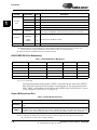
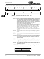
Table 1-2: EP73xx Internal Registers (Little Endian Mode)
Address
Name
0x8000.0000
PADR
0
RW
8
Port A data register
page 11-1
0x8000.0001
PBDR
0
RW
8
Port B data register
page 11-1
0x8000.0002
—
—
8
Reserved
0x8000.0003
PDDR
0
RW
8
Port D data register
page 11-1
0x8000.0040
PADDR
0
RW
8
Port A data direction register
page 11-1
0x8000.0041
PBDDR
0
RW
8
Port B data direction register
page 11-1
0x8000.0042
—
—
8
Reserved
0x8000.0043
PDDDR
0
RW
8
Port D data direction register
page 11-1
0x8000.0080
PEDR
0
RW
3
Port E data register
page 11-1
0x8000.00C0
PEDDR
0
RW
3
Port E data direction register
page 11-1
0x8000.0100
SYSCON1
0
RW
32
System control register 1
page 5-4
0x8000.0140
SYSFLG1
0
RD
32
System status flags register 1
page 5-9
0x8000.0180
MEMCFG1
0
RW
32
Expansion memory configuration register 1
page 8-3
0x8000.01C0
MEMCFG2
0
RW
32
Expansion memory configuration register 2
page 8-5
0
RW
32
Reserved
0x8000.0200
Default RD/WR
Size
Comments
Page
0x8000.0240
INTSR1
0
RD
32
Interrupt status register 1
page 4-8
0x8000.0280
INTMR1
0
RW
32
Interrupt mask register 1
page 4-10
0x8000.02C0
LCDCON
0
RW
32
LCD control register
page 9-7
0x8000.0300
TC1D
0
RW
16
Read / Write register sets and reads data to TC1
page 3-3
0x8000.0340
TC2D
0
RW
16
Read / Write register sets and reads data to TC2
page 3-3
0x8000.0380
RTCDR
—
RW
32
Real Time Clock data register
page 3-3
0x8000.03C0
RTCMR
—
RW
32
Real Time Clock match register
page 3-4
0x8000.0400
PMPCON
0
RW
12
PWM pump control register
page 12-3
0x8000.0440
CODR
0
RW
8
CODEC data I/O register
page 16-20
0x8000.0480
UARTDR1
0
RW
16
UART1 FIFO data register
page 17-5
0x8000.04C0
UBRLCR1
0
RW
32
UART1 bit rate and line control register
page 17-6
0x8000.0500
SYNCIO
0
RW
32
Synchronous serial I/O data register for master only SSI
page 15-4
1-4
Copyright Cirrus Logic, Inc. 2003
EP7309/11/12 User’s Manual - DS508UM4
Introduction
Address
Name
Default RD/WR
Size
Comments
Page
0x8000.0540
PALLSW
0
RW
32
Least significant 32-bit word of LCD palette register
page 9-8
0x8000.0580
PALMSW
0
RW
32
Most significant 32-bit word of LCD palette register
page 9-8
0x8000.05C0
STFCLR
—
WR
—
Write to clear all start up reason flags
page 5-13
0x8000.0600
BLEOI
—
WR
—
Write to clear battery low interrupt
page 4-13
0x8000.0640
MCEOI
—
WR
—
Write to clear media changed interrupt
page 4-13
0x8000.0680
TEOI
—
WR
—
Write to clear tick and watchdog interrupt
page 4-13
0x8000.06C0
TC1EOI
—
WR
—
Write to clear TC1 interrupt
page 4-13
0x8000.0700
TC2EOI
—
WR
—
Write to clear TC2 interrupt
page 4-14
0x8000.0740
RTCEOI
—
WR
—
Write to clear RTC match interrupt
page 4-14
0x8000.0780
UMSEOI
—
WR
—
Write to clear UART modem status changed interrupt
page 4-14
0x8000.07C0
COEOI
—
WR
—
Write to clear CODEC sound interrupt
page 4-14
0x8000.0800
HALT
—
WR
—
Write to enter the Idle State
page 2-14
0x8000.0840
STDBY
—
WR
—
Write to enter the Standby State
page 2-13
0x8000.0880–
0x8000.0FFF
Reserved
0x8000.1000
FBADDR
0xC
RW
4
LCD frame buffer start address
page 9-9
0x8000.1100
SYSCON2
0
RW
16
System control register 2
page 5-7
0x8000.1140
SYSFLG2
0
RD
24
System status register 2
page 5-12
0x8000.1240
INTSR2
0
RD
16
Interrupt status register 2
page 4-11
0x8000.1280
INTMR2
0
RW
16
Interrupt mask register 2
page 4-12
0x8000.12C0–
0x8000.147F
Reserved
0x8000.1480
UARTDR2
0
RW
16
UART2 Data Register
page 17-5
0x8000.14C0
UBRLCR2
0
RW
32
UART2 bit rate and line control register
page 17-6
0x8000.1500
SS2DR
0
RW
16
Master / slave SSI2 data Register
page 16-20
0x8000.1600
SRXEOF
—
WR
—
Write to clear RX FIFO overflow flag
page 4-14
0x8000.16C0
SS2POP
—
WR
—
Write to pop SSI2 residual byte into RX FIFO
page 16-20
0x8000.1700
KBDEOI
—
WR
—
Write to clear keyboard interrupt
page 4-14
0x8000.1800
Reserved
—
WR
—
Do not write to this location. A write will cause the
processor to go into an unsupported power savings
state.
0x8000.1840–
0x8000.1FFF
Reserved
—
0x8000.2000
DAIR
0
RW
32
DAI control register
page 16-12
0x8000.2040
DAIR0
0
RW
32
DAI data register 0
page 16-14
0x8000.2080
DAIDR1
0
RW
32
DAI data register 1
page 16-15
0x8000.20C0
DAIDR2
0
WR
21
DAI data register 2
page 16-16
0x8000.2100
DAISR
0
RW
32
DAI status register
page 16-16
0x8000.2200
SYSCON3
0
RW
16
System control register 3
page 5-8
0x8000.2240
INTSR3
0
RD
32
Interrupt status register 3
page 4-12
0x8000.2280
INTMR3
0
RW
8
Interrupt mask register 3
page 4-13
Write will have no effect, read is undefined
Write will have no effect, read is undefined
Write will have no effect, read is undefined
EP7309/11/12 User’s Manual - DS508UM4
Copyright Cirrus Logic, Inc. 2003
1-5
11
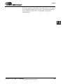
Table 1-2: EP73xx Internal Registers (Little Endian Mode) (Continued)
1
Introduction
Table 1-2: EP73xx Internal Registers (Little Endian Mode) (Continued)
1
Address
Name
0x8000.22C0
LEDFLSH
0
RW
7
LED Flash register
page 13-2
0x8000.2300
SDCONF
2
RW
32
SDRAM Configuration Register
page 7-3
0x8000.2340
SDRFPR
128
RW
16
SDRAM Refresh Register
page 7-4
0x8000.2440
UNIQID
0
R
32
32-bit unique ID for the EP73xx device
page 5-13
0x8000.2600
DAI64Fs
0
RW
32
DAI 64Fs Control Register
page 16-11
0x8000.2610
PLLW
W
8
Write Register for PLL Multiplier
page 2-11
0x8000.A5A8
PLLR
R
Read Register for PLL Multiplier
page 2-11
0x8000.2700
RANDID0
0
R
32
Bits 31-0 of 128-bit random ID for the EP73xx device
page 5-13
0x8000.2704
RANDID1
0
R
32
Bits 63-32 of 128-bit random ID for the EP73xx device
page 5-13
0x8000.2708
RANDID2
0
R
32
Bits 95-64 of 128-bit random ID for the EP73xx device
page 5-13
0x8000.270C
RANDID3
0
R
32
Bits 127-96 of 128-bit random ID for the EP73xx device
page 5-13
All other address
space that is not
assigned to a
register listed in
this table
Default RD/WR
Size
Comments
Page
All addresses that are outside the address space of the
registers listed in this table are reserved. The undefined
areas contain test registers used during manufacturing
tests. Writes to this area should never be attempted
during normal operation as this may cause unexpected
behavior. Any read from this register will be undefined.
Reserved
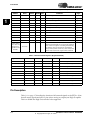
Table 1-3: EP73xx Internal Registers (Big Endian Mode)
Big Endian Mode
Name
Default
RD/WR
Size
Comments
0x0000.0083
PEDR
0
RW
3
Port E Data Register
0X8000.00C3
PEDDR
0
RW
3
Port E Data Direction Register
0x8000.0000
PDDR
0
RW
8
Port D Data Register
0x8000.0001
—
—
8
Reserved
0x8000.0002
PBDR
0
RW
8
Port B Data Register
0x8000.0003
PADR
0
RW
8
Port A Data Register
0x8000.0040
PDDDR
0
RW
8
Port D Data Direction Register
0x8000.0041
—
—
8
Reserved
0x8000.0042
PBDDR
0
RW
8
Port B Data Direction Register
0x8000.0043
PADDR
0
RW
8
Port A data Direction Register
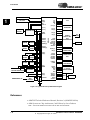
Pin Description
Table 1-4 on page 1-7 describes the function of all external signals to the EP73xx. Note
that all output signals and all I/O pins (when acting as outputs) are High-Z capable.
This is to enable the High-Z test modes to be supported.
1-6
Copyright Cirrus Logic, Inc. 2003
EP7309/11/12 User’s Manual - DS508UM4
Introduction
11
External Signal Functions
Table 1-4: External Signal Functions
Function
Signal Name
Signal
Data bus
D[0-31]
I/O
32-bit system data bus for memory, SDRAM, and I/O interface
A[0-31]
O
32 bits of system byte address during memory and expansion cycles
A[27-13]/
DRA[0-14]
O
DRA[0-14] are multiplexed with A[27-13] for SDRAM memory accesses. A27
corresponds to DRA0 on SDRAM device. This offers additional power savings since
the lightest loading is expected on the high order ROM address lines.
Whenever the EP73xx is in the Standby State, the external address and data buses
are driven low. The RUN signal is used internally to force these buses to be driven
low. This is done to prevent peripherals that are powered-down from draining current.
Also, the internal peripheral’s signals get set to their Reset State.
BA[0-1]/
A[13-14]
I/O
A13 and A14, during SDRAM accesses, become bank select pins BA0 and BA1.
nMOE/nSDCAS
O
ROM expansion OP enable/ SDRAM CAS control signal
nMWE/nSDWE
O
ROM expansion write enable/ SDRAM write enable control signal
nCS[0-5]
O
Chip select; active low, SRAM-like chip selects for expansion
SDQM[0-1]
O
LDQM; lower byte masks for SDRAM accesses
SDQM[2-3]
O
UDQM; upper byte masks for SDRAM/ multiplexed with PD[6-7]. See GPIO section
SDCS[0-1]
O
SDRAM chip selects
EXPRDY
I
Expansion port ready; external expansion devices drive this low to extend the bus
cycle. This is used to insert wait states for an external bus cycle.
WRITE/nSDRAS
O
Transfer Direction for expansion bus/SDRAM RAS control signal during SDRAM
access
Address bus
Description
1
To do write accesses of different sizes Word and Half-Word must be externally
decoded. The encoding of these signals is as follows:
Memory Interface
WORD/
HALFWORD
O
Access Size
Word
Half-Word
Word
1
0
Half-Word
0
1
Byte
0
0
The core will generate an address. When doing a read, the ARM core will select the
appropriate byte channels. When doing a write, the correct bytes will have to be
enabled depending on the above signals and the least significant bits of the address
bus.
The ARM architecture does not support unaligned accesses. For a read using x 32
memory, it is assumed that you will ignore bits 1 and 0 of the address bus and
perform a word read (or in power critical systems decode the relevant bits depending
on the size of the access). If an unaligned read takes place, the core will rotate the
resulting data in the register. For more information on this behavior see the LDR
instruction in the ARM7TDMI data sheet.
EP7309/11/12 User’s Manual - DS508UM4
Copyright Cirrus Logic, Inc. 2003
1-7
Introduction
Table 1-4: External Signal Functions (Continued)
Function
Signal Name
Signal
Description
External Clock
EXPCLK
I/O
Expansion clock rate is the same as the CPU clock for 13 MHz and 18 MHz. It runs
at 36.864 MHz for 36,49 and 74 MHz modes; in 13 MHz mode this pin is used as the
clock input.
1
Interrupts
Power
Management
nMEDCHG/
nBROM
I
Media changed input; active low, deglitched. Used as a general purpose FIQ
interrupt during normal operation. It is also used on power up to configure the
processor to either boot from the internal Boot ROM, or from external memory.
When low, the chip will boot from the internal Boot ROM.
nEXTFIQ
I
External active low fast interrupt request input
EINT[3]
I
External active high interrupt request input
nEINT[1-2]
I
Two general purpose, active low interrupt inputs
nPWRFL1
I
Power fail input; active low, deglitched input to force system into the Standby State
BATOK1
I
Main battery OK input; falling edge generates a FIQ, a low level in the Standby State
inhibits system start up; deglitched input
nEXTPWR
I
External power sense; must be driven low if the system is powered by an external
source
nBATCHG1
I
New battery sense; driven low if battery voltage falls below the "no-battery"
threshold; it is a deglitched input
I
Power-on reset input. This signal is not deglitched. When active it completely resets
the entire system, including all the RTC registers. Upon power-up, the signal must be
held active low for a minimum of 100 µsec. after VDD has settled. During normal
operation, nPOR needs to be held low for at least one clock cycle of the selected
clock speed (i.e., when running at 13 MHz, the pulse width of nPOR needs to be >
77 nsec).
Note that nURESET, TEST[0], TEST[1], PE[0], PE[1], PE[2], DRIVE[0], DRIVE[1],
nMEDCHG, are all latched on the rising edge of nPOR.
O
This pin is programmed to either output the RUN signal or the CLKEN signal. The
CLKENSL bit is used to configure this pin. When RUN is selected, the pin will be
high when the system is active or idle, low while in the Standby State. When CLKEN
is selected, the pin will only be driven low when in the Standby State (For RUN, see
Table 1-6 on page 1-10).
I
Wake up is a deglitched input signal. It must also be held high for at least 125 µsec to
guarantee its detection. Once detected it forces the system into the Operating State
from the Standby State. It is only active when the system is in the Standby State.
This pin is ignored when the system is in the Idle or Operating State. It is used to
wakeup the system after first power-up, or after software has forced the system into
the Standby State. WAKEUP will be ignored for up to two seconds after nPOR goes
HIGH. Therefore, the external WAKEUP logic must be designed to allow it to rise and
stay HIGH for at least 125 usec, two seconds after nPOR goes HIGH.
nPOR
RUN/CLKEN
State Control
WAKEUP1
User reset input; active low deglitched input from user reset button.
DAI, CODEC or
SSI2 Interface
(See Table 1-5 on
page 1-10 for pin
assignment and
direction following
multiplexing)
1-8
nURESET1
I
SSICLK
I/O
DAI/CODEC/SSI2 clock signal
SSITXFR
I/O
DAI/CODEC/SSI2 serial data output frame/synchronization pulse output
SSITXDA
O
DAI/CODEC/SSI2 serial data output
SSIRXDA
I
DAI/CODEC/SSI2 serial data input
SSIRXFR
I/O
This pin is also latched upon the rising edge of nPOR and read along with the input
pins nTEST[0-1] to force the device into special test modes. nURESET does not
reset the RTC.
SSI2 serial data input frame/synchronization pulse
DAI/CODEC external clock input
Copyright Cirrus Logic, Inc. 2003
EP7309/11/12 User’s Manual - DS508UM4
Introduction
11
Table 1-4: External Signal Functions (Continued)
Function
ADC
Interface
(SSI1)
IrDA and
RS232
Interfaces
LCD
Keyboard &
Buzzer drive
LED Flasher
General
Purpose I/O
PWM
Drives
Signal Name
Signal
Description
ADCCLK
O
Serial clock output
nADCCS
O
Chip select for ADC interface
ADCOUT
O
Serial data output
ADCIN
I
Serial data input
SMPCLK
O
Sample clock output
LEDDRV
O
Infrared LED drive output (UART1)
PHDIN
I
Photo diode input (UART1)
TXD[1-2]
O
RS232 UART1 and 2 TX outputs
RXD[1-2]
I
RS232 UART1 and 2 RX inputs
DSR
I
RS232 DSR input
DCD
I
RS232 DCD input
CTS
I
RS232 CTS input
DD[0-3]
I/O
LCD serial display data; pins can be used on power up to read the ID of some LCD
modules (See Table 1-6 on page 1-10).
CL[1]
O
LCD line clock
CL[2]
O
LCD pixel clock
FRM
O
LCD frame synchronization pulse output
M
O
LCD AC bias drive
COL[0-7]
O
Keyboard column drives (SYSCON1)
BUZ
O
Buzzer drive output (SYSCON1)
PD[0]/
LEDFLSH
O
LED flasher driver — multiplexed with Port D bit 0. This pin can provide up to 4 mA
of drive current.
PA[0-7]
I/O
Port A I/O (bit 6 for boot clock option); also used as keyboard row inputs
PB[0-7]
I/O
Port B I/O. All eight Port B bits can be used as GPIOs.
PD[0-5]
I/O
Port D I/O / PD0 multiplexed at LEDFLSH. See above.
PD[6-7]/SDQM
[0-1]
I/O
Port D I/O/dedicated byte mask select for SDRAM
PE[0]/
BOOTSEL[0]
I/O
Port E I/O (3 bits only). Can be used as general purpose I/O during normal
operation.
PE[1]/
BOOTSEL[1]
I/O
During power-on reset, PE[0] and PE[1] are inputs and are latched by the rising edge
of nPOR to select the memory width that the EP73xx will use to read from the boot
code storage device (i.e., external 8-bit-wide FLASH bank).
PE[2]/
CLKSEL
I/O
During power-on reset, PE[2] is latched by the rising edge of nPOR to select the
clock mode of operation (i.e., either the PLL or external 13 MHz clock mode).
DRIVE[0-1]
I/O
PWM drive outputs. These pins are inputs on power up to determine what polarity
the output of the PWM should be when active. Otherwise, these pins are always an
output (See Table 1-6 on page 1-10).
FB[0-1]
I
1
PWM feedback inputs
EP7309/11/12 User’s Manual - DS508UM4
Copyright Cirrus Logic, Inc. 2003
1-9
Introduction
Table 1-4: External Signal Functions (Continued)
Function
1
Boundary
Scan
Test
Signal Name
Signal
Description
TDI
I
JTAG data in
TDO
O
JTAG data out
TMS
I
JTAG mode select
TCLK
I
JTAG clock
nTRST
I
JTAG async reset
nTEST[0-1]
I
Test mode select inputs. These pins are used in conjunction with the power-on
latched state of nURESET to select between the various device test models.
MOSCIN
MOSCOUT
I
O
Main 3.6864 MHz oscillator for 18.432 MHz–90.3168 MHz PLL
RTCIN
RTCOUT
I
O
Real Time Clock 32.768 kHz oscillator
Oscillators
No Connects
N/C
No connects should be left as no connects; do not connect to ground
1. All deglitched inputs are via the 16.384 kHz clock. Each deglitched signal must be held active for at least two clock
periods. Therefore, the input signal must be active for at least ~125 µs to be detected cleanly.
The RTC crystal must be populated for the device to function properly.
DAI/CODEC/SSI2 Pin Multiplexing
Table 1-5: SSI/CODEC/DAI Pin Multiplexing
SSI2
CODEC
DAI
Direction
Strength
SSICLK
PCMCLK
SCLK
I/O
1
SSITXFR
PCMSYNC
LRCK
I/O
1
SSITXDA
PCMOUT
SDOUT
Output
1
SSIRXDA
PCMIN
SDIN
Input
SSIRXFR
p/u*
MCLK
I/O
1
* p/u = use an ~10 k pull-up
The selection between SSI2 and the CODEC is controlled by the state of the SERSEL
bit in SYSCON2 (See SYSCON2 System Control Register 2). The choice between the
SSI2, CODEC, and the DAI is controlled by the DAISEL bit in SYSCON3 (See “System
Control Register 3 (SYSCON3)” on page 5-8).
Output Bi-Directional Pins
Table 1-6: Output Bi-Directional Pins
RUN
Drive [0-1]
DD[0-3]
The RUN pin is looped back in to skew the address and data bus from each other.
Drive 0 and 1 are looped back in on power up to determine what polarity the output of the PWM should be when
active.
DD[0-3] are looped back on power up to bits 7:4 of the SYSFLG1 register. Pin values are latched upon the enabling of
the LCD Controller via the LCDEN bit. This is useful for reading the panel ID of some LCD modules. When some LCD
modules are reset, they will output a panel ID onto these pins. See the SYSFLG1 register for more information.
The above output pins are implemented as bi-directional pins to enable the output side of the pad to be monitored and
hence provide more accurate control of timing or duration.
1-10
Copyright Cirrus Logic, Inc. 2003
EP7309/11/12 User’s Manual - DS508UM4
Introduction
11
Block Diagrams
13-MHz INPUT
3.6864 MHz
INTERNAL DATA BUS
PLL
D[0-31]
ARM720T
32.768 kHz
MEMORY CONTROLLER
32.768-kHz
OSCILLATOR
ARM7TDMI
CPU CORE
nPOR, RUN,
RESET, WAKEUP
STATE
CONTROL
BATOK, EXTPWR
PWRFL, BATCHG
POWER
MANAGEMENT
EINT[1-3], FIQ,
MEDCHG
INTERRUPT
CONTROLLER
FLASHING LED DRIVE
MMU
SDRAM CNTRL
GPIO
DC TO DC
PWM
ADCCLK, ADCIN,
ADCOUT,
SMPCLK, ADCCS
SSI1
TIMER
COUNTERS(2)
MaverickKey™
EPB BRIDGE
EPB BUS
ICE-JTAG
LCD
CONTROLLER
DAI
CODEC
A[0-27],
DRA[0-14]
LCD
ON-CHIP
BOOT ROM
SSI2
MOE, MWE, SDCLK,
SDQM[0-3], SDRAS,
SDCAS
INTERNAL ADDRESS BUS
WRITE
BUFFER
RTC
PORTS A, B, D (8-BIT)
PORT E (3-BIT)
KEYBD DRIVERS (0-7)
SSICLK, SSITXFR,
SSITXDA, SSIRXDA,
SSIRSFR
EXPANSION CNTRL
8-KBYTE
CACHE
EXPCLK, WORD, nCS[0-3],
EXPRDY, WRITE
ON-CHIP
SRAM
48 KBYTES
UART1
UART2
TEST AND
DEVELOPMENT
LCD DRIVE
IrDA
LED AND
PHOTODIODE
ASYNC
INTERFACE 1
ASYNC
INTERFACE 2
Figure 1-1. EP73xx Block Diagram
EP7309/11/12 User’s Manual - DS508UM4
Copyright Cirrus Logic, Inc. 2003
1-11
1
Introduction
1
CRYSTAL
MOSCIN
DD[0-3]
CRYSTAL
RTCIN
nCS[4]
PB0
EXPCLK
CL1
CL2
FRM
M
LCD
COL[0-7]
PC CARD
CONTROLLER
PC CARD
SOCKET
KEYBOARD
D[0-31]
A[0-27]
PA[0-7]
PB[0-7]
nMOE
WRITE
PD[0-7]
SDRAS/
SDCAS
×16
SDRAM
×16
SDRAM
SDCS[0]
×16
SDRAM
×16
SDRAM
SDCS[1]
SDQM[0-3]
SDQM[0-3]
EP73XX
PE[0-2]
POWER
SUPPLY UNIT
AND
COMPARATORS
nPOR
nPWRFL
BATOK
nEXTPWR
nBATCHG
RUN
WAKEUP
BATTERY
DRIVE[0-1]
DC-TO-DC
CONVERTERS
FB[0-1]
nCS[0]
nCS[1]
×16
FLASH
×16
FLASH
SSICLK
SSITXFR
SSITXDA
SSIRXDA
SSIRXFR
×16
FLASH
×16
FLASH
LEDDRV
PHDIN
CS[n]
WORD
EXTERNAL MEMORYMAPPED EXPANSION
BUFFERS
nCS[2]
nCS[3]
ADDITIONAL I/O
BUFFERS
AND
LATCHES
LEDFLSH
DC
INPUT
CODEC/SSI2/
DAI
IR LED AND
PHOTODIODE
RXD1/2
TXD1/2
DSR
CTS
DCD
2× RS-232
TRANSCEIVERS
ADCCLK
nADCCS
ADCOUT
ADCIN
SMPCLK
ADC
DIGITIZER
Figure 1-2. Typical EP73xx System Block Diagram
References
• ARM720T Technical Reference Manual, Revision 3 (ARM DDI 0192A)
• ARM System-on-Chip Architecture, 2nd Edition, by Steve Furberu
Note: Click on the ARM Documentation site to view more documents.
1-12
Copyright Cirrus Logic, Inc. 2003
EP7309/11/12 User’s Manual - DS508UM4
2CPU Core
22
Chapter 2
2
Introduction
The 7312 processor utilizes the ARM720T which is based on the ARM7TDMI RISC
(Reduced Instruction Set Computer) core running at a dynamically programmable
speed from 18-90 MHz. This chapter discusses the key features of the ARM core.
Features
Key features include:
• ARM7TDMI CPU core (which supports the logic for the Thumb instruction
set, core debug, enhanced multiplier, JTAG, and the Embedded ICE)
running at a dynamically programmable clock speeds.
• Memory Management Unit (MMU) compatible with the ARM710 core
(providing address translation and a 64-entry translation lookaside buffer)
with added support for Windows CE.
• 8 Kbytes of unified instruction and data cache with a four-way set
associative cache controller.
• Write Buffer
• TLB (Translation Look-Aside Buffer)
• System State Control: Operating, Idle, Standby
• CPU Clock Options
• System Reset Options
• CPU and Co-processor Registers
Programming Register List
Table 2-1: Programming Registers
Address
Name
Type
0x8000.0840
STDBY
0x8000.0800
Description
Page
Write
Write Enters Standby State
page 2-13
HALT
Write
Write enters Idle State
page 2-13
0x8000.2610
PLL
Write
8
Write register for PLL Multiplier
page 2-11
0x8000.A5A8
PLL
Read
8
Read Register for PLL Multiplier
page 2-11
EP7309/11/12 User’s Manual - DS508UM4
Size
Copyright Cirrus Logic, Inc. 2003
2-1
CPU Core
Block Diagram
Detailed block diagram of the core is shown below.
2
V ir tu a l A d d re s s B u s
MMU
8 K by te C a c h e
A R M 7 TD M I
CPU
C o p ro ce sso r
In te rfa ce
In te rn a l D a ta B u s
W rite B u ffe r
JT A G
D ebug
In te rfa ce
S y ste m
C o n tro l
C o p ro ce sso r
A M BA
In te rfa ce
A M BA
a d d re ss
AM BA
d a ta
Figure 2-1. ARM720T Block Diagram
Programming Examples
;*****************************************************************************
; Set up the MMU. Start by flushing the cache and TLB.
;*****************************************************************************
;
ldr
r0, =0x00000000
mcr
p15, 0, r0, c5, c0 ; co-processor register c5
mcr
p15, 0, r0, c7, c0 ; co-processor register c7
;
;*****************************************************************************
; Set user mode access for all 16 domains.
;*****************************************************************************
2-2
Copyright Cirrus Logic, Inc. 2003
EP7309/11/12 User’s Manual - DS508UM4
CPU Core
22
;
ldr
mcr
;
r0, =0x55555555
p15, 0, r0, c3, c0 ; co-processor register c3
;*****************************************************************************
2
; Tell the MMU where to find the page table.
;*****************************************************************************
;
IMPORT PageTable
ldr
r0, =PageTable
mcr
p15, 0, r0, c2, c0 ; co-processor register c2
;
;*****************************************************************************
; Enable the MMU.
;*****************************************************************************
;
ldr
mcr
;
r0, =0x0000007d ; Cache and Write Buffer enabled in the command
p15, 0, r0, c1, c0 ; co-processor register c1
;*****************************************************************************
; There should always be two NOP instructions following the enable or
; disable of the MMU.
;*****************************************************************************
;
mov
mov
;
r0, r0
r0, r0
;*****************************************************************************
; System state control registers. Standby and Idle states can be entered by
; writes to these register locations.
;*****************************************************************************
;
ldr
r0 , =0x80000000 ; base address for Standby and Idle(Halt) registers
mov
str
r1, #0xAA ; value to be written to registers
r1, [r0,#0x0840] ; write to Standby - system will now enter Standby
state
str
r1, [r0,#0x0800] ; write to Idle(Halt) - system, will now enter Idle
state
;
EP7309/11/12 User’s Manual - DS508UM4
Copyright Cirrus Logic, Inc. 2003
2-3
CPU Core
Operational Overview
Using the Von Neumann (load/store) architecture, the ARM720T core has a three
stage instruction pipeline to increase the speed of the instruction execution within the
processor. The fetch-decode-execute of concurrent instructions are done in parallel
requiring approximately 1.9 CPI (cycles per instruction).
2
The core provides a 8 Kbytes unified cache and a memory management unit (MMU).
The MMU supports a two-level page table arrangement and controls the cache and
write buffer for each page created.
ARM720T core has 37 32-bit registers: 1-program counter, 1-current program status
register, 5-saved program status registers, 30-general purpose registers. The core also
supports 16 co-processor registers for control of the on-chip cache, MMU, and buffers.
The core supports two instruction sets, ARM and Thumb for full 32-bit or 16-bit
instruction decoding. State switching between ARM and Thumb, and register
assignments for each, are detailed in the ARM720T document provided by ARM. The
core supports both big as well as little-endian modes.
The core contains an embedded debug architecture. The 5-pin JTAG port will allow
the host system to convert debugger commands into JTAG commands for the
purpose of hardware control to do the following:
• Set breakpoints and watchpoints
• Halt the ARM processor
• Access internal registers
• Access system memory
MMU
The MMU (Memory Management Unit) does the following
• Translates virtual addresses to physical addresses
• Controls memory access permissions, cache and write buffer accesses for
each page.
The MMU consists of a TLB (translation look aside buffer) and hardware for page
table accesses as well as the access control logic.
Memory is divided by the MMU in the following manner:
• Sections: 1 Mbyte memory blocks
• Large Page: 64 Kbytes memory blocks which allows mapping of large
region with only a single entry in the TLB.
• Small Page: 4 Kbytes memory blocks
Based on the entry for the section or page, the cache and write buffer will be either
enabled or disabled for that region of memory.
2-4
Copyright Cirrus Logic, Inc. 2003
EP7309/11/12 User’s Manual - DS508UM4
CPU Core
The TLB (Translation look-aside Buffer) is a 64-entry associative cache of recent
virtual address to physical address translations to eliminate a two-stage search for a
higher proportion of internal register or external bus accesses.
• Provides the translation and access permission information for memory
accesses
• For a TLB miss, the TLB walking hardware accesses the transition table
from physical memory to update itself (two-stage).
• If the TLB is full, a stored value will be over-written.
Cache
Cache is 4-way set associative with 8 Kbytes of mixed instruction and data, organized
as 512 lines of 4 words (16-byte). Connected directly to the core, cache only stores the
virtual address. Cache can only be used once the MMU is enabled. Once enabled, the
specific sections or pages of memory that are segmented can control whether cache or
write buffer is used for that region. Cache is disabled at power on reset. See Figure
2-2 on page 2-6 for cache organization.
EP7309/11/12 User’s Manual - DS508UM4
Copyright Cirrus Logic, Inc. 2003
2-5
22
TLB
2
CPU Core
31
11
10
4 3 2 1 0
v irtu a l a d d re ss
2
by te
a d d re sse s
ta g R A M
ta g R A M
ta g R A M
[1:0]
ta g R A M
[8:2]
D a ta R A M
[10:0]
1 2 8 e n try
1 2 8 en try
1 2 8 e n try
1 2 8 e n try
=?
=?
=?
=?
[10:9]
2 0 4 8 x 3 2 -b it
w o rd
e n co d e
h it
d a ta
Figure 2-2. ARM720T Cache Organization
Cache is direct-mapped. The copy of the address or data is stored along with an
address tag that is compared with the location in system memory. Cache is also writethrough and uses a replacement algorithm to select which of the four possible
locations will be overwritten in the case of a cache miss.
Write Buffer
The write buffer holds four addresses and eight data words.The MMU defines which
addresses are bufferable. Each address can be associated with any number of data
words. Data words are written to sequential memory starting at that address.
The write buffer becomes full when all four addresses are used or all eight data words
are used. The processor can write into the write buffer at fast cache speed and
continue executing instructions stored in cache while the write buffer stores data to
external memory at the current memory bus speed. If there is a memory fault
generated by a buffered write, the system will not be able to recover from it since the
processor state is not recoverable.
2-6
Copyright Cirrus Logic, Inc. 2003
EP7309/11/12 User’s Manual - DS508UM4
CPU Core
JTAG (Joint Test Action Group) or IEEE 1149 provides a boundary scan test interface
with 5 dedicated signals connected directory to the CPU core:
2
• TRST - Test Reset (active low)
• TCK - Test Clock
• TMS - Test Mode Select
• TDI - Test Data In
• TDO - Test Data Out
See Chapter 14 for more information on debugging the EP73xx via the JTAG interface.
CPU Register Definitions
ARM has 37 32-bit internal registers. If operating in Thumb mode, the processor must
switch to ARM mode before taking an exception. The return instruction will restore
the processor to Thumb state. Most tasks are executed out of User mode.
User:
Unprivileged normal operating mode.
FIQ:
Fast interrupt (high priority) mode when FIQ is asserted
IRQ:
Interrupt request (normal) mode when IRQ is asserted
Supervisor: Software interrupt instruction (SWI) or reset will cause entry into
this mode
Abort:
Memory access violation will cause entry into this mode
Undef:
Undefined instructions
System:
Privileged mode. Uses same registers as user mode
Figure 2-3 on page 2-8 illustrates the use of all registers for the following core
operating modes. Each will bank or store a specific number of registers. Banked
register information is not shared between modes. FIQs bank the fewest number of
registers which increases performance.
EP7309/11/12 User’s Manual - DS508UM4
Copyright Cirrus Logic, Inc. 2003
22
Debug Interface
2-7
CPU Core
U se r
F IQ
IR Q
SV C
U nd ef
A bo r t
r0
2
r1
r2
r3
r4
Banked
T h u m b s ta te
L ow r e g iste rs
r5
r6
Banked
B a n k ed
B anked
Banked
r7
r8
r8
r9
r9
r1 0
r1 0
r1 1
r1 1
r1 2
r1 2
r 1 3 (s p )
r 1 3 (sp )
r 1 3 (s p )
r1 3 (sp )
r1 3 (sp )
r 1 3 (sp )
r 1 4 (lr )
r 1 4 (lr)
r 1 4 (lr )
r1 4 (lr )
r1 4 (lr)
r 1 4 (lr)
sp s r
sp s r
s p sr
s p sr
sp sr
T h u m b s ta te
H ig h re g is te r s
r1 5 (p c)
c p sr
Figure 2-3. Register Organization Summary
User mode in Thumb state generally limits access to r0-r7. There are a few
instructions that allow access to the high registers. For the 5 exceptions, the processor
must revert to ARM state.
R0-R12:
General purpose read/write 32-bit registers
R13 (sp):
Stack Pointer
R14 (lr):
Link Register
R15 (pc):
Program Counter
CPSR:
Current Program Status Register (contains condition codes and
operating modes)
SPSR:
Saved Program Status Register (saves CPSR when exception occurs)
ARM720T Core Coprocessor Registers
The ARM720T core has 16 coprocessor registers for control over the MMU. See Table
2-2 on page 2-9 Updates to the co-processor registers are written using the CP15
instruction.
2-8
Copyright Cirrus Logic, Inc. 2003
EP7309/11/12 User’s Manual - DS508UM4
CPU Core
22
Table 2-2: ARM720T Core Coprocessor Registers
Register
Description
0
ID Register (Read/Write) register than may return an ID consisting of an
architecture version and ARM trademark
1
Control (Read/Write) register to enable MMU, cache, write buffer, and other
coprocessor operations
2
Translation Base Table (Read/Write) register contains the start address of the first
level translation table
3
Domain Access Control (Read/Write) register specifies permissions for all 16
domains
4
Reserved
5
Fault Status (Read/Write) register indicates type of fault and domain of last data
abort. Write to this location flushes entire TLB.
6
Fault Address (Read/Write) register contains address of the last data access abort
7
Cache Operation (Write) register will configure or perform a clean (flush) of the
cache and write buffer when written to
8
TLB Operation (Write) register can configure or clean (flush) when written to
9-12
2
Reserved
13
Used to support WinCE. Returns a logic “1” if WinCE enhancements are enabled.
14-15
Reserved
CPU Clocks
There are two clocks required to maintain any of the processor states that will be
described in the following section.
• Real Time Clock (RTC)
• On-chip PLL (Phase Lock Loop) Clock
• External 13 MHz Clock (Optional)
Real Time Clock (RTC)
The RTC is generated from an external 32 kHz crystal oscillator created by the crystals
fundamental tone. The RTC, from the crystal will be clocked at 1 Hz. Internally, it
contains a match and data registers that are updated once per second. More
information is contained in Chapter 3 of the manual.
Real Time Clock Characteristics and Interface Requirements
• The external crystal connects directly to the RTCIN and RTCOUT pins on the
processor.
• 32.768 kHz frequency should be created by the fundamental tone of the
external crystal.
EP7309/11/12 User’s Manual - DS508UM4
Copyright Cirrus Logic, Inc. 2003
2-9
CPU Core
• Start-up resistor is not necessary. One is provided internally.
• Start-up capacitors may be placed on each side of the external crystal and
ground. Value for each should be around 10 pF but also should be selected
based upon crystal specifications. Capacitance of the traces and crystal
leads should be subtracted from the load capacitor value for precision.
2
• The crystal should have a maximum of 5 ppm frequency drift over the
chips’s operating temperature range.
• Voltage for the crystal must be 2.5 V+ 0.2 V.
A digital clock source can be used to drive the RTCIN on the EP73xx. Voltage levels of
the clock should match that of Vdd supply for the processor pads or the supply
voltage used to drive the non-core Vdd pins on the EP73xx. In this configuration, the
output clock pin should be left floating.
On-Chip PLL
The on-chip PLL is generated from an external 3.686 MHz crystal. The ARM720T
CPU clock, from the PLL, can then be programmed to 18.432, 36.864, 49.152, 73.728,
and 90.3168 MHz.
The external bus is controlled by the PLL and defaults to 18 MHz until the internal
CPU clock reaches 36 MHz or above, at which point the external bus runs at 1/2 the
CPU clock speed. Modifying the PLL speed in the SYSCON3 register will require a
NOP at the next instruction for the system to stabilize. Internally, the state controller
switches from the current clock to the new clock speed, by bringing both clocks low,
then perform the switch to the new speed to insure a glitch-free transition.
PLL Clock Characteristics and Interface Requirements
• The 3.6864 MHz frequency should be created by the crystals fundamental
tone.
• Start-up resistor is provided internally
• Value of loading capacitors should be in the range of 10 pF. However, the
actual value will depend on the crystal’s specifications. The total sum of the
capacitance on the pins and the leads should factor into the value of the
loading capacitors.
• The crystal should have a maximum of 10 ppm frequency drift over the
operating temperature of the chip.
A digital clock source can be used to drive the MOSCIN pin of the EP73xx. Voltage
levels of the clock source should match the Vdd supply for the EP73xx non-core pins.
The output clock pin (MOSCOUT) should be left floating.
PLL Multiplier for 90 MHz Operation
There are two internal register that can be used to increase the PLL frequency beyond
74 MHz. The intention is to increase the speed to 90 MHz for use with the DAI and to
increase overall performance. This can affect devices and their times running from the
2-10
Copyright Cirrus Logic, Inc. 2003
EP7309/11/12 User’s Manual - DS508UM4
CPU Core
22
internal PLL clock so adjustments and consideration will need to be taken into
account.
PLL Equation: (PLL Multiplier/2)* 3.686 MHz = PLL Frequency
ex. For 90 MHz operation, PLL Multiplier = 49
It should be noted that using the PLL Multiplier to achieve 90 MHz operation will
result in a shifting up of frequencies and rates derived from the PLL by 22.5%. For
example, the data bus will move from 36 MHz to 45 MHz. Take care when using a
PLL-derived system because such shifting may be in effect.
Programming Example
;********************************************************************************
; Sample code for entering the proper value into the PLL Multiplier Write Register
to
; achieve 90 MHz operation. This is done after setting the PLL to 74 MHz in
; SYSCON3.
;********************************************************************************
;begin
PLL_Multiplier_Write_Register EQU 0x80002610; the location of the PLL multiplier
;Write register
Value_For_90_MHz_Operation EQU 0x31000000
; the value for 90Mhz operation
ldr r0= PLL_Multiplier_Write_Register
ldr r1= Value_For_90_MHz_Operation
str r1, [r0]
; store R1 at R0
; end
PLL Register Descriptions
PLL Multiplier Write Register (PLLW)
Address:
0x8000.2610, Write Only
Definition:
PLL Multiplier is written to the upper 8 bits of this register only. Do
not read from this location
PLL Multiplier Read Register (PLLR)
Address:
0x8000.A5A8, Read Only
Definition:
PLL Multiplier value written to above register can be read at this
location in the upper 8 bit only. Do not write to this location.
Note: Increasing the PLL clock too high will cause the processor to abort any
operation. Decreasing the speed will not clear the condition. A system reset and
a lower setting will be required. PLL must be preset to 74MHz via SYSCON3
before PLL multiplier can be used properly.
External 13 MHz Clock
An external 13 MHz crystal oscillator can be used to drive the EP73xx. When selected,
the CPU and external buses are both clocked at 13 MHz. In this configuration, the
EP7309/11/12 User’s Manual - DS508UM4
Copyright Cirrus Logic, Inc. 2003
2-11
2
CPU Core
internal PLL is not used. The default value “00” for the PLL setting in SYSCON3 must
not change.
2
CPU State Control
There are three principal power management states on the EP73xx processor
• Operating State (highest power consumption)
• Idle State
• Standby State (lowest power consumption)
Interrupt or rising wakeup
Standby
Operating
Write to standby location,
power fail, or user reset
rr
te
In
nPOR, power fail,
or user reset
t
up
Idle
Write to halt location
Figure 2-4. State Diagram
Each state leaves on or turns off a unique set of CPU peripherals which can serve to
reduce or limit the power required for the system for blocks of time in which there is
no external system activity. The processor can enter or exit any one of the three states.
Standby State
Standby state is the lowest power state the processor can achieve and still be capable
of returning to operating state or equates to the system being switched off. The RTC
clock remains on to insure that the processor can “wake up” from an external
interrupt or the “wake up” signal.
When the EP73xx is first powered on, the processor is in a “cold reset”. The same
condition can be created by asserting nPOR . Cold reset for the processor is the
standby state. In this instance, none of the peripherals have been initialized so the
only method for entering the operating state is by means of the WAKEUP pin.
Clock Status
• If internal PLL is used, it will shut off
• If external 13 MHz clock is being used, CPU will ignore input. External
2-12
Copyright Cirrus Logic, Inc. 2003
EP7309/11/12 User’s Manual - DS508UM4
CPU Core
• RTC remains on.
Entering standby state can be accomplished in software by writing to the STDBY
register, or in hardware with input from the nURESET or by nPWRFL.
Before entering the standby state, the software must properly disable the DAI. Failing
to do so will result in higher than expected power consumption while in this state as
well as unpredictable behavior of the DAI.
During standby state, all system memory and state are maintained and the system
time is kept up-to-date. The external address and data bus are forced low internally
by the RUN signal which is also driven low. This is done to prevent peripherals that
are powered down from draining current. Since the RUN signal is driven low, it can
also be used to disable external devices to further reduce power drain while in this
state. The internal peripherals external signals return to their reset state.
Exiting standby is accomplished with the following external stimulus of a keyboard
interrupt (if enabled), power management inputs, external interrupts EINT[3:1], or
WAKEUP.
The following register will allow the system software to put the processor into
Standby state. Writing to this location will not clear the internal registers settings of
the processor. The processor will sit until an external interrupt or the WAKEUP pin is
asserted and continue executing code from the point of entry into Standby.
State Control Register Descriptions
Enter the Standby State Register (STDBY)
Address:
0x8000.0840, Write Only
Definition:
A write to this location will put the system into the Standby State by
halting the main oscillator. A write to this location while there is an
active interrupt will have no effect.
Note: Before entering the Standby State, the LCD Controller should be disabled. The
LCD controller should be enabled on exit from the Standby State. If the EP73XX
is attempting to get into the Standby State when there is a pending interrupt
request, it will not enter into the low power mode. The instruction will get
executed, but the processor will ignore the command.
Idle State
From operating state, the processor can enter Idle state by writing to the HALT
register of the EP73xx. When an interrupt occurs, the processor will return to the
operating state and execute the next instruction. WAKEUP cannot be used.
In the Idle state, the device will function as it would in operating state with the
exception of the CPU clock which is halted. The PLL (if enabled) or the external
13 MHz clock source will remain active during this state.
EP7309/11/12 User’s Manual - DS508UM4
Copyright Cirrus Logic, Inc. 2003
2-13
22
logic (CLKEN ) pin can be used to disable external oscillator if desired. In
this configuration,
2
CPU Core
The following register will allow the system software to put the processor into Idle
state.
Enter the Idle State Register (HALT)
2
Address:
0x8000.0800, Write Only
Definition:
A write to this location will put the system into the Idle State by
halting the clock to the processor until an interrupt is generated. A
write to this location while there is an active interrupt will have no
effect
Below is a list of peripherals and clocks and their status during each of the three
states:
Table 2-3: Status of Peripherals and Clocks by Operating State
Address (W/B)
Operating
Idle
nPOR
RESET
Standby
nURESET
RESET
SDRAM Control
On
On
SELFREF
Off
N/A
UARTs
On
On
Off
Reset
Reset
LCD FIFO
On
On
Reset
Reset
Reset
LCD
On
On
Off
Reset
Reset
ADC Interface
On
On
Off
Reset
Reset
SSI2 Interface
On
On
Off
Reset
Reset
DAI Interface
On
On
Off
Reset
Reset
CODEC
On
On
Off
Reset
Reset
Timers
On
On
Off
Reset
Reset
RTC
On
On
On
On
On
LED Flasher
On
On
On
Reset
Reset
DC-to-DC
On
On
Off
Reset
Reset
CPU
On
Off
Off
Reset
Reset
Interrupt Control
On
On
On
Reset
Reset
PLL/CLKEN Signal
On
On
Off
Off
Off
Power Up Sequence
The EP73xx has a power-up sequence that must be followed for a proper start. If any
of the recommended timing sequences below are violated, the part may not start
properly and may not recover without a hard reset.
1. Upon power-up, nPOR must be held low for a minimum of 100 µs after
Vdd has settled
Note: nURESET must be stable before nPOR rising.
2-14
Copyright Cirrus Logic, Inc. 2003
EP7309/11/12 User’s Manual - DS508UM4
CPU Core
3. After nPOR goes high, the WAKEUP signal will be detected by the processor
after one to two seconds. After such time, the WAKEUP (active high) signal
can be detected but must be asserted high for a minimum of 125 µs
Note: IMPORTANT. nURESET must not be asserted during the period between
WAKEUP assertion and transition from Standby to Operating state. This will
cause the processor to enter an unknown state and require a system reset to
clear this condition.
4. Once the WAKEUP signal is detected internally, it first enters a deglitching
circuit which is the reason for the 125 µs duration. The PLL is then enabled
and the CPU turns on. WAKEUP signal is then ignored and will only be
read again after a nPOR assertion or power is cycled on the device at which
time the EP73xx will return to Standby. WAKEUP is also ignored during
Idle state.
5. Once the WAKEUP signal has been detected, a maximum of 250 ms will
elapse before the CPU is turned on and begins fetching the first instruction.
RESET
There are three asynchronous resets to the EP73xx: nPOR, nPWRFL, and nURESET. If
any of these are active, a system reset is generated internally. This will reset all
internal registers in the EP73xx except the RTC data and match registers. These
registers are only cleared by nPOR .
Any reset will also reset the CPU and cause it to start execution at the reset vector
(address 0x0) when the EP73xx returns to the operating state.
Internal to the EP73xx, three different signals are used to reset the storage elements.
These are nPOR , nSYSRES, and nSTDBY.
nPOR (active low) is the highest priority reset signal and is also the external signal
that forces the internal signals nSYSRES and nSTDBY (equivalent to the external RUN
signal) active. nPOR will only be active after the EP73xx has first powered up and not
during any other resets. nPOR active will clear all flags in the status register except for
the cold reset flag (CLDFLG) which is bit 15 of the SYSFLG register.
nSYSRES (System Reset, active low) is generated internally to the EP73xx if nPOR ,
nPWRFL, or nURESET are active. It is the second highest priority reset signal, used to
asynchronously reset most internal registers in the EP73xx. nSYSRES (when active)
forces nSTDBY and RUN low which is the result of the CPU resetting and the EP73xx
going into Standby. This can be done without co-operation from the system software.
The nSTDBY and RUN signals are high when the EP73xx is in Operating or Idle state.
The nSTDBY will disable any peripheral block that is clocked from the CPU clock
except the RTC.
EP7309/11/12 User’s Manual - DS508UM4
Copyright Cirrus Logic, Inc. 2003
2-15
22
2. Once nPOR goes high, the EP73xx will enter Standby State. In this state, the
PLL is not enabled and thus the CPU is not turned on. The WAKEUP signal
must be asserted
2
CPU Core
2
This page intentionally blank.
2-16
Copyright Cirrus Logic, Inc. 2003
EP7309/11/12 User’s Manual - DS508UM4
3Timers
33
Chapter 3
3
Introduction
EP73xx has three general purpose timers that can serve as watchdogs for system
resources or and events. Two timers are based on the internal PLL or 13 MHz clock
and the third is fed by the RTC. Routines requiring periodic service to check status
and new values can make use of these timers.
Features
All timers have the following characteristics
• Programmable for two modes: free running and pre-scale
• Interrupt flags and corresponding mask for control and status
• Timer 16-bit read/write data register to set and read values. Can be
accessed at any time.
Timer Register List
Table 3-1: Timer Registers
Address
Name
Type
Size
Description
Page
0x8000.0300
TC1D
R/W
16
TC1 Data Register
page 3-3
0x8000.0340
TC2D
R/W
16
TC2 Data Register
page 3-3
0x8000.0380
RTCDR
R/W
32
RTC Data Register
page 3-3
0x8000.03C0
RTCMR
R/W
32
RTC Match Register
page 3-4
Programming Example
;*****************************************************************************
; Enable TC1 Timer prescale = 2 kHz Program a 2 ms interrupt rate
;*****************************************************************************
;
TC1Prescale
EQU 0x10
;
TC1Timer
EQU 0x14
;
TC1Mask
EQU
0x100 ;
ldr
r12, =0x80000000
ldr
r1, =TC1Prescale
EP7309/11/12 User’s Manual - DS508UM4
Set prescale in SYSCON1
Set 10 ms timer in TC1 timer
UnMask TC1 interrupt
; base address for Timers
Copyright Cirrus Logic, Inc. 2003
3-1
Timers
str
ldr
str
ldr
str
;
3
r1,
r1,
r1,
r0,
r0,
[r12, #0x0100] ; Prescale - 2 kHz clock
=TC1Timer
[r12, #0x300] ; 10 ms timer rate
=TC1Mask
[r12,#0x0280] ; Interrupt enabled
Operational Overview
These identical count-down timers derive their clock from the internal PLL or
external 13 MHz clock. Values for these timers are programmed into the read/write
registers as seen below and are decremented on the second active edge of the clock
once the write to the register is complete (i.e., after the first complete period of the
clock). When the timer reaches 0, the corresponding interrupt is asserted (if enabled).
Values can be written to the data registers at any time.
When running from the PLL clock, 512 kHz and 2 kHz rates are possible for each
timer. When using the external 13 MHz crystal, the default frequencies for the timers
will be 541 and 2.115 kHz. Optionally, in 13 MHz mode, a divider of 26 can be used to
generate a frequency of 500 kHz. This is set automatically in 13 MHz mode by setting
the OSTB bit in SYSCON2 register thus routing a 500 kHz clock to the timer. This
however, does not affect the frequencies derived for any of the other internal
peripherals.
Setting the clock source frequency for TC1 and TC2 involves writes to SYSCON1 bit 5
and 7. Clearing each bit sets the clock to 2 kHz. Setting this bit sets the clock at
512 kHz.
Interrupts masks for these registers are set in the INTMR1 register and status seen in
the INTSR1 register. To clear the interrupt for TC1 and TC2, a write to the TE2EOITC1 and TE2EOI-TC2 registers respectively will clear the underflow interrupt.
When operating at 90 Mhz, the two timers deriving their clocks from the PLL will be
shifted upwards by 22.5%. Therefore the 512 kHz clock will become 627.2 kHz and
the 2 kHz clock will become 2.45 kHz. The timer deriving its clock from the RTC is not
affected.
Free Running Mode
In free running mode, the counter will wrap around to 0xFFFF when it underflows
and will continue to count down. Any value written will be decremented on the
second edge of the selected clock rate. A value of 0 in bit 4 or 6 of SYSCON1 will set
free running mode for TC1 and TC2 respectively.
3-2
Copyright Cirrus Logic, Inc. 2003
EP7309/11/12 User’s Manual - DS508UM4
Timers
33
Prescale Mode
Any value written to TC1 or TC2 is automatically re-loaded when the counter
underflows. Any value written to TC1 or TC2 will be decremented on the second
edge of the selected clock. Setting bit 4 or 6 in SYSCON1 for TC1 and TC2
respectively, will initiate prescale mode.
3
RTC Timer
The RTC timer is derived from the RTC clock. The timer interface creates a 1 Hz tick
that can be controlled by the RTCDR (RTC data register). This 32-bit read/write
register value corresponds to the number of 1 Hz ticks and will be incremented on the
next rising edge of the 1 Hz clock. Any value may be written to this register.
The interrupt driven from this clock comes from the RTCMR (RTC Match Register).
Once the value in the match register actually “matches” the value in the data register,
the interrupt will assert.
Timer Register Descriptions
Timer Counter 1 Data Register (TC1D)
Address:
0x8000.0300, Read/Write
Definition:
The timer counter 1 data register is a 16-bit read/write register
which sets and reads data to TC1. Any value written will be
decremented on the next rising edge of the clock.
Timer Counter 2 Data Register(TC2D)
Address:
0x8000.0340, Read/Write
Definition:
The timer counter 2 data register is a 16-bit read/write register
which sets and reads data to TC2. Any value written will be
decremented on the next rising edge of the clock
Real Time Clock Data Register (RTCDR)
Address:
0x8000.0380, Read/Write
Definition:
The Real Time Clock data register is a 32-bit read/write register,
which sets and reads the binary time in the RTC. Any value written
will be incremented on the next rising edge of the 1 Hz clock. This
register is reset only by nPOR .
EP7309/11/12 User’s Manual - DS508UM4
Copyright Cirrus Logic, Inc. 2003
3-3
Timers
Real Time Clock Match Register (RTCMR)
3
3-4
Address:
0x8000.03C0, Read/Write
Definition:
The Real Time Clock match register is a 32-bit read/write register,
which sets and reads the binary match time to RTC. Any value
written will be compared to the current binary time in the RTC, if
they match it will assert the RTCMI interrupt source. This register is
reset only by nPOR.
Copyright Cirrus Logic, Inc. 2003
EP7309/11/12 User’s Manual - DS508UM4
4Interrupt Controller
44
Chapter 4
4
Introduction
Like most modern microprocessors, the EP73xx contains an interrupt controller to
manage both external and internal exceptions. When an expected or unexpected
event arises during the execution of a program (i.e. interrupt or memory fault) an
exception is generated. If more than one exception occurs at the same time, a fixed
priority system determines the order in which they are handled.
Features
• Interrupt requests received from 22 different sources
• Standard (IRQ) and Fast (FIQ) interrupt types
• Interrupts can be used to wake the CPU from IDLE or STANDBY
Interrupt Register List
Table 4-1: Interrupt Registers
Address
Name
Type
Size
Description
Page
0x8000.0240
INTSR1
RO
32
Interrupt Status
page 4-8
0x8000.1240
INTSR2
R/W
32
Interrupt Status
page 4-11
0x8000.2240
INTSR3
R/W
32
Interrupt Status
page 4-12
0x8000.0280
INTMR1
R/W
32
Interrupt Mask
page 4-10
0x8000.1280
INTMR2
R/W
32
Interrupt Mask
page 4-12
0x8000.2280
INTMR3
R/W
32
Interrupt Mask
page 4-13
0x8000.0600
BLEOI
R/W
---
Battery Low EOI
page 4-13
0x8000.0640
MCEOI
R/W
---
Media Change EOI
page 4-13
0x8000.0680
TEOI
R/W
---
Tick Watchdog EOI
page 4-13
0x8000.06C0
TC1EOI
R/W
---
TC1 EOI
page 4-13
0x8000.0700
TC2EOI
R/W
---
TC2 EOI
page 4-14
0x8000.0740
RTCEOI
R/W
---
RTC Match EOI
page 4-14
0x8000.0780
UMSEOI
R/W
---
UART1 Modem EOI
page 4-14
EP7309/11/12 User’s Manual - DS508UM4
Copyright Cirrus Logic, Inc. 2003
4-1
Interrupt Controller
Table 4-1: Interrupt Registers (Continued)
4
Address
Name
Type
Size
Description
Page
0x8000.07C0
COEOI
R/W
---
CODEC EOI
page 4-14
0x8000.1700
KBDEOI
R/W
---
Keyboard EOI
page 4-14
0x8000.1600
SRXEOF
R/W
---
SSI2 FIFO EOI
page 4-14
Programming Examples
ENTRY
;
ldr
ldr
ldr
r15, ResetV
r15, UndefV
r15, SWIV
ldr
r15, PAbortV
ldr
r15, DAbortV
ldr
r15, UnusedV
ldr
r15, IRQV
ldr
r15, FIQV
;
;*****************************************************************************
; The following is the actual vector table. It contains the addresses of the routines
; which handle each exception type.
;*****************************************************************************
ResetV
DCD
ResetHandler ; (0x0)
UndefV
DCD
UndefHandler ; (0x4)
SWIV
DCD
SWIHandler ; (0x8)
DCD
PAbortHandler ; (0xc)
DCD
DAbortHandler ; (0x10)
DCD
UnusedHandler ; (0x14)
DCD
IRQHandler ; (0x18)
DCD
FIQHandler ; (0x1C)
PAbortV
DAbortV
UnusedV
IRQV
FIQV
;*****************************************************************************
; IRQHandler routine checks for Timer1 expire interrupt. Sets GPIO PA0-8 low
; Interrupt cleared before return to program.
;*****************************************************************************
IRQHandler
TIMERCHECK
EQU
0x00000100
ldr
r0, =0x80000000 ; base address for interrupt status register
ldr
r1, [r0,#0x240] ; r1 contains timer status from INTSR1
cmp
r1, #TIMERCHECK
4-2
Copyright Cirrus Logic, Inc. 2003
EP7309/11/12 User’s Manual - DS508UM4
Interrupt Controller
44
bne
mov
strb
mov
str
nextstatuscheck ; not the timer - moving down the IRQ routine
r2, #0x0
r2, [r0,#0x0] ; setting PA0-8 low
r2, #0xFFFFFFFF
r2, [r0,0x06C0] ; Write to TC1EOI register - clear interrupt
4
; ........ code...........
subs
;
pc, lr, #4 ; Return from interrupt to pending instruction
Operational Overview
Once an exception occurs, the ARM720T will attempt to complete the current
instruction (except for a system reset) and will then identify the interrupt type. The
interrupt vector table, already loaded by the system software contains a reference or
address of the specific interrupt routine for each type of exception identified by the
processor. The CPU will jump to the appropriate routine for servicing of the interrupt.
The vector table for all interrupt types is as follows:
Table 4-2: Vector Addresses by Interrupt Type
Interrupt
Vector Address
Reset
0x0
Undefined Instruction
0x4
Software Interrupt (SWI)
0x8
Prefetch Abort (Instruction fetch)
0xC
Data abort (Data access)
0x10
IRQ (normal interrupt)
0x18
FIQ (fast interrupt)
0x1C
Within each routine for each interrupt type created by the system software, the
specific interrupt can be determined by examining any one of the three status
registers. After an action is taken, a write to the appropriate “End of Interrupt”
register must be issued to clear the interrupt status register to prevent re-entry and an
endless loop.
For several interrupts occurring simultaneously, the pre-determined priority based on
type of interrupt will cause the highest interrupt priority to execute first and queue
any remaining interrupts. Interrupts of the same type that occur simultaneously
simply require system software to check all possible interrupts for the specific type.
EP7309/11/12 User’s Manual - DS508UM4
Copyright Cirrus Logic, Inc. 2003
4-3
Interrupt Controller
Interrupt Types and Priorities
The EP73xx interrupt controller can generate two types of interrupts: Standard (IRQ)
or Fast (FIQ). Seventeen of the twenty-two interrupt sources are IRQ interrupts, while
the remaining five are FIQ. FIQs have a higher priority than IRQs. If two interrupts
are received from within the same group (IRQ or FIQ), the order in which they are
serviced must be resolved in software. The priorities are listed in Table 4-3.
4
Table 4-3: Exception Priority Handling
Priority
Exception
Highest
Reset
.
Data Abort
.
FIQ
.
IRQ
.
Prefetch Abort
Lowest
Undefined Instruction, Software Interrupt
Interrupt Operation
All interrupts are level sensitive; that is, they must conform to the following
sequence:
1. The interrupting device (either external or internal) asserts the appropriate
interrupt.
2. If the appropriate bit is set in the interrupt mask register, then either an FIQ
or an IRQ will be asserted by the interrupt controller. (Descriptions of each
bit in this register can be found in “Interrupt Status Register 1 (INTSR1)”
on page 4-8.)
3. If interrupts are enabled, the processor jumps to the appropriate address.
4. Within the interrupt handler routine, the status register is read to
determine if the source of the interrupt(s). This will determine which
subroutine(s) to call to service said interrupt(s).
5. Software in the interrupt service routine will clear the interrupt source by
an action specific to the device requesting the interrupt (i.e., reading the
UART RX register).
The interrupt service routine may then re-enable interrupts; other pending interrupts
are serviced in a similar way. Alternately, the service routine may return to the
interrupt dispatch code, which can check for pending interrupts and dispatch them
accordingly. The “End of Interrupt” type interrupts are latched. All other interrupt
sources (i.e., external interrupt source) must be held active until its respective service
routine starts executing. See “End-Of-Interrupt Locations” on page 4-13 for more
details.
4-4
Copyright Cirrus Logic, Inc. 2003
EP7309/11/12 User’s Manual - DS508UM4
Interrupt Controller
Table 4-4, Table 4-5, and Table 4-6 show the names and allocation of interrupts in the
EP73xx.
4
Table 4-4: Interrupt Allocation in the First Interrupt Register
Interrupt
Bit in INTMR1
and INTSR1
Name
FIQ
0
EXTFIQ
FIQ
1
BLINT
Battery low interrupt
FIQ
2
WEINT
Tick Watchdog expired interrupt
FIQ
3
MCINT
Media changed interrupt
IRQ
4
CSINT
CODEC sound interrupt
IRQ
5
EINT1
External interrupt input 1 (nEINT[1] pin)
IRQ
6
EINT2
External interrupt input 2 (nEINT[2] pin)
IRQ
7
EINT3
External interrupt input 3 (EINT[3] pin)
IRQ
8
TC1OI
TC1 underflow interrupt
IRQ
9
TC2OI
TC2 underflow interrupt
IRQ
10
RTCMI
RTC compare match interrupt
IRQ
11
TINT
IRQ
12
UTXINT1
Internal UART1 transmit FIFO empty interrupt
IRQ
13
URXINT1
Internal UART1 receive FIFO full interrupt
IRQ
14
UMSINT
Internal UART1 modem status changed interrupt
IRQ
15
SSEOTI
Synchronous serial interface 1 end of transfer interrupt
Comment
External fast interrupt input (nEXTFIQ pin)
64 Hz tick interrupt
Table 4-5: Interrupt Allocation in the Second Interrupt Register
Interrupt
Bit in INTMR2 and
INTSR2
Name
IRQ
0
KBDINT
Key press interrupt
IRQ
1
SS2RX
Master / slave SSI 16 bytes received
IRQ
2
SS2TX
Master / slave SSI 16 bytes transmitted
IRQ
12
UTXINT2
UART2 transmit FIFO empty interrupt
IRQ
13
URXINT2
UART2 receive FIFO full interrupt
Comment
Table 4-6: Interrupt Allocation in the Third Interrupt Register
Interrupt
Bit in INTMR3 and
INTSR3
Name
FIQ
0
DAIINT
EP7309/11/12 User’s Manual - DS508UM4
Comment
DAI interface interrupt
Copyright Cirrus Logic, Inc. 2003
44
Interrupt Listing
4-5
Interrupt Controller
Interrupt Latencies in Different States
Operating State
The ARM720T processor checks for a low level on its FIQ and IRQ inputs at the end of
each instruction. The interrupt latency is therefore directly related to the amount of
time it takes to complete execution of the current instruction when the interrupt
condition is detected. There is a one to two clock cycle synchronization penalty
following the assertion of the interrupt. For example, if the EP73xx is operating at
13 MHz with a 16-bit external memory system, and instruction sequence stored in
one wait state FLASH memory, the worst-case interrupt latency is 251 clock cycles.
This delay will include:
4
• Instruction fetch to complete LDM r0!, (r0-r15) worst case. This is a quad
word quad instruction burst on the memory bus.
• Time for interrupt signal(data abort)
• Write Buffer flush (result of LDM instruction)
• 3 TLB misses (worst case)
• 6 cache misses (worst case)
• 1 additional cache and MMU miss due to fetch from vector space
The ARM720T processor, operating at 13 MHz, has a worst-case interrupt latency of
about 19.3 ms in the example system. For those interrupt inputs which have deglitching, the interrupt latency is increased by the maximum time required to pass
through the deglitcher, which is approximately 125 µs (2 cycles of the 16.384 kHz
clock derived from the RTC oscillator). Adding the deglitcher creates an absolute
worst-case latency of approximately 141 ms. If the ARM720T is run at 36 MHz or
greater, the 19.3 ms value will be reduced.
All serial data transfer peripherals included in the EP73xx (except the master-only
SSI1) have local buffering to ensure a reasonable interrupt latency response
requirement for the OS of 1 ms or less. This assumes that the design data rates do not
exceed the data rates described in this specification. If the OS cannot meet this
requirement, there will be a risk of data over/underflow occurring.
Idle State
When leaving the Idle State as a result of an interrupt, the CPU clock is restarted after
approximately two clock cycles. However, there is potentially up to 20 ms latency as
described above, unless the code is written to include at least two single cycle
instructions immediately after the write to the IDLE register (in which case the
latency drops to a few microseconds).
This is important, as the Idle State can only be left because of a pending interrupt,
which has to be synchronized by the processor before it can be serviced.
4-6
Copyright Cirrus Logic, Inc. 2003
EP7309/11/12 User’s Manual - DS508UM4
Interrupt Controller
The Standby State equates to the system being switched “off” (i.e., no display, and the
main oscillator is shut down). If the 18.432–73.72 MHz mode is selected, the PLL will
be shut down. In the 13 MHz mode, if the CLKENSL bit is set low, the CLKEN signal
will be forced low and can, if required, be used to disable an external oscillator.
In Standby State, all system memory and state is maintained and system time is kept
current. The PLL/on-chip oscillator or external oscillator is disabled and the system is
static, except for the low-power watch crystal (32 kHz) oscillator and divider chain to
the RTC and LED flasher. The RUN signal is driven low, and can be used externally in
the system to power down other system modules.
When the EP73xx is in Standby State, external address and data buses are driven low.
The RUN signal is used internally to force these buses to be driven low. This is done to
prevent peripherals that are power-down from draining current.
In Standby State, internal peripherals’ signals are set to their Reset States.
Table 4-7 summarizes the five external interrupt sources and the effect they have on
the processor interrupts.
Table 4-7: External Interrupt Sources
Interrupt
Pin
nEXTFIQ
Input State
Operating
State Latency
Idle State Latency
Standby State Latency
Not deglitched; must be
Worst-case
active for 20 µs to be
latency of 20 µs
detected
Worst-case 20 µs: if only
single cycle instructions,
less than 1 µs
Including PLL / osc. settling time,
approx. 0.25 sec, or approx. 500
µs when in Idle State if in 13 MHz
mode with CLKENSL set
Worst-case 20 µs: if only
single cycle instructions,
less than 1 µs
Including PLL / osc. settling time,
approx. 0.25 sec, or approx. 500
µs when in Idle State if in 13 MHz
mode with CLKENSL set.
Including PLL / osc. settling time,
approx. 0.25 sec, or approx. 500
µs when in Idle State if in 13 MHz
mode with CLKENSL set.
nEINT1–2
Not deglitched
Worst-case
latency of 20 µs
EINT3
Not deglitched
Worst-case 20 µs: if only
Worst-case
single cycle instructions,
latency of 19.3 µs
less than 1 µs
nMEDCHG
Deglitched by
16.384 kHz clock; must
be active for at least
122 µs to be detected
Worst-case
latency of 141 µs
EP7309/11/12 User’s Manual - DS508UM4
Worst-case latency
141 µs; if any single cycle
instructions = 125 µs
Copyright Cirrus Logic, Inc. 2003
As above (note difference if in
13 MHz mode with CLKENSL set)
4-7
44
Standby State
4
Interrupt Controller
Interrupt Register Descriptions
Interrupt Status Register 1 (INTSR1)
4
31
30
29
28
27
26
25
24
23
22
21
20
19
18
17
16
RSVD
15
14
13
12
11
10
9
8
7
6
5
4
3
2
1
0
SSEOTI
UMSINT
URXINT1
UTXINT1
TINT
RTCMI
TC2OI
TC1OI
EINT3
EINT2
EINT1
CSINT
MCINT
WEINT
BLINT
EXTFIQ
Address:
0x8000.0240, Read Only
Definition:
The interrupt status register is a 32-bit read only register. The
interrupt status register reflects the current state of the first 16
interrupt sources within the EP73xx. Each bit is set if the appropriate
interrupt is active. The interrupt assignment is given below.
Bit Descriptions:
RSVD:
Unknown during Read.
EXTFIQ:
External fast interrupt. This interrupt will be active if the nEXTFIQ
input pin is forced low and is mapped to the FIQ input on the
ARM720T processor.
BLINT:
Battery low interrupt. This interrupt will be active if no external
supply is present (nEXTPWR is high) and the battery OK input pin
BATOK is forced low. This interrupt is de-glitched with a 16 kHz
clock, so it will only generate an interrupt if it is active for longer
than 125 µs. It is mapped to the FIQ input on the ARM720T
processor and is cleared by writing to the BLEOI location. BLINT
is disabled during The Standby State.
WEINT:
Tick Watch dog expired interrupt. This interrupt will become
active on a rising edge of the periodic 64 Hz tick interrupt clock if
the tick interrupt is still active (i.e., if a tick interrupt has not been
serviced for a complete tick period). It is mapped to the FIQ input
on the ARM720T processor and the TEOI location.
Note: WEINT and watchdog timer are disabled during the Standby State. The watch
dog timer tick rate is 64 Hz (in 13 MHz and 73.728–18.432 MHz modes).
4-8
Copyright Cirrus Logic, Inc. 2003
EP7309/11/12 User’s Manual - DS508UM4
Interrupt Controller
Media changed interrupt. This interrupt will be active after a
rising edge on the nMEDCHG input pin has been detected, This
input is de-glitched with a 16 kHz clock so it will only generate an
interrupt if it is active for longer than 125 µs. It is mapped to the
FIQ input on the ARM7TDMI processor and is cleared by writing
to the MCEOI location. On power-up, the Media change pin
(nMEDCHG) is used as an input to force the processor to either
boot from the internal Boot ROM, or from external memory. After
power-up, the pin can be used as a general purpose FIQ interrupt
pin.
CSINT:
CODEC sound interrupt, generated when the data FIFO has
reached half full or empty (depending on the interface direction).
It is cleared by writing to the COEOI location.
EINT1:
External interrupt input 1. This interrupt will be active if the
nEINT1 input is active (low). It is cleared by returning nEINT1 to
the passive (high) state.
EINT2:
External interrupt input 2. This interrupt will be active if the
nEINT2 input is active (low). It is cleared by returning nEINT2 to
the passive (high) state.
EINT3:
External interrupt input 3. This interrupt will be active if the EINT3
input is active (high). It is cleared by returning EINT3 to the
passive (low) state.
TC1OI:
TC1 under flow interrupt. This interrupt becomes active on the
next falling edge of the timer counter 1 clock after the timer
counter has under flowed (reached zero). It is cleared by writing
to the TC1EOI location.
TC2OI:
TC2 under flow interrupt. This interrupt becomes active on the
next falling edge of the timer counter 2 clock after the timer
counter has under flowed (reached zero). It is cleared by writing
to the TC2EOI location.
RTCMI:
RTC compare match interrupt. This interrupt becomes active on
the next rising edge of the 1 Hz Real Time Clock (one second later)
after the 32-bit time written to the Real Time Clock match register
exactly matches the current time in the RTC. It is cleared by
writing to the RTCEOI location.
TINT:
64 Hz tick interrupt. This interrupt becomes active on every rising
edge of the internal 64 Hz clock signal. This 64 Hz clock is derived
from the 15-stage ripple counter that divides the 32.768 kHz
oscillator input down to 1 Hz for the Real Time Clock. This
interrupt is cleared by writing to the TEOI location. TINT is
disabled/turned off during the Standby State.
EP7309/11/12 User’s Manual - DS508UM4
Copyright Cirrus Logic, Inc. 2003
4-9
44
MCINT:
4
Interrupt Controller
UTXINT1: Internal UART1 transmit FIFO half-empty interrupt. The function
of this interrupt source depends on whether the UART1 FIFO is
enabled. If the FIFO is disabled (FIFOEN bit is clear in the UART1
bit rate and line control register), this interrupt will be active when
there is no data in the UART1 TX data holding register and be
cleared by writing to the UART1 data register. If the FIFO is
enabled this interrupt will be active when the UART1 TX FIFO is
half or more empty, and is cleared by filling the FIFO to at least
half full. The FIFO is 16 bytes deep.
4
URXINT1: Internal UART1 receive FIFO half full interrupt. The function of
this interrupt source depends on whether the UART1 FIFO is
enabled. If the FIFO is disabled this interrupt will be active when
there is valid RX data in the UART1 RX data holding register and
be cleared by reading this data. If the FIFO is enabled this
interrupt will be active when the UART1 RX FIFO is half or more
full or if the FIFO is non empty and no more characters have been
received for a three character time out period. It is cleared by
reading all the data from the RX FIFO. The FIFO is 16 bytes deep.
UMSINT:
Internal UART1 modem status changed interrupt. This interrupt
will be active if either of the two modem status lines (CTS or DSR)
change state. It is cleared by writing to the UMSEOI location.
SSEOTI:
Synchronous serial interface end of transfer interrupt. This
interrupt will be active after a complete data transfer to and from
the external ADC has been completed. It is cleared by reading the
ADC data from the SYNCIO register.
Interrupt Mask Register 1 (INTMR1)
31
30
29
28
27
26
25
24
23
22
21
20
19
18
17
16
RSVD
15
14
13
12
11
10
9
8
7
6
5
4
3
2
1
0
SSEOTI
UMSINT
URXINT1
UTXINT1
TINT
RTCMI
TC2OI
TC1OI
EINT3
EINT2
EINT1
CSINT
MCINT
WEINT
BLINT
EXTFIQ
4-10
Address:
0x8000.0280, Read / Write
Definition:
This interrupt mask register is a 32-bit read/write register, used to
selectively enable any of the first 16 interrupt sources within the
EP73xx. Interrupts associated with bits 0 through 3 generate a fast
interrupt request to the ARM720T processor (FIQ), causing a jump
to processor virtual address 0000.001C. All other interrupts generate
a standard interrupt request (IRQ), causing a jump to processor
virtual address 0000.0018. Set the appropriate bit in this register to
enable the corresponding interrupt. All bits are cleared by a system
reset. Consult the bit definitions for INTSR1 for information about
interrupts associated with each mask bit.
Copyright Cirrus Logic, Inc. 2003
EP7309/11/12 User’s Manual - DS508UM4
Interrupt Controller
31
30
29
28
27
26
25
24
23
22
21
20
19
18
17
16
7
6
5
4
3
2
1
0
SS2TX
SS2RX
KBDINT
RSVD
15
14
RSVD
13
12
URXINT2
UTXINT2
11
10
9
8
RSVD
Address:
0x8000.1240, Read / Write
Definition:
This register is an extension of INTSR1. This interrupt status register
also reflects the current state of the new interrupt sources within the
EP73xx. Each bit is set if the appropriate interrupt is active. The
interrupt assignment is given below.
Bit Descriptions:
RSVD:
Unknown during Read.
KBDINT:
Keyboard interrupt. This interrupt is generated whenever a key is
pressed, from the logical OR of the first 6 or all 8 of the Port A
inputs (depending on the state of the KBD6 bit in the SYSCON2
register. The interrupt request is latched and can be de-asserted by
writing to the KBDEOI location. KBDINT is not deglitched.
SS2RX:
Synchronous serial interface 2 receives FIFO half or greater full
interrupt. This is generated when RX FIFO contains 8 or more
half-words. This interrupt is cleared only when the RX FIFO is
emptied or one SSI2 clock after RX is disabled.
SS2TX:
Synchronous serial interface 2 transmit FIFO less than half empty
interrupt. This is generated when TX FIFO contains fewer than
8 byte pairs. This interrupt gets cleared by loading the FIFO with
more data or disabling the TX. One synchronization clock is
required when disabling the TX side before it takes effect.
UTXINT2: UART2 transmit FIFO half empty interrupt. The function of this
interrupt source depends on whether the UART2 FIFO is enabled.
If the FIFO is disabled (FIFOEN bit is clear in the UART2 bit rate
and line control register), this interrupt will be active when there
is no data in the UART2 TX data holding register and be cleared
by writing to the UART2 data register. If the FIFO is enabled, this
interrupt will be active when the UART2 TX FIFO is half or more
empty and is cleared by filling the FIFO to at least half full. The
FIFO is 16 bytes deep.
EP7309/11/12 User’s Manual - DS508UM4
Copyright Cirrus Logic, Inc. 2003
4-11
44
Interrupt Status Register 2 (INTSR2)
4
Interrupt Controller
URXINT2: UART2 receive FIFO half full interrupt. The function of this
interrupt source depends on whether the UART2 FIFO is enabled.
If the FIFO is disabled, this interrupt will be active when there is
valid RX data in the UART2 RX data holding register and be
cleared by reading this data. If the FIFO is enabled, this interrupt
will be active when the UART2 RX FIFO is half or more full or if
the FIFO is non-empty, and no more characters have been received
for a three-character time-out period, it is cleared by reading all
the data from the RX FIFO. The FIFO is 16 bytes deep.
4
Interrupt Mask Register 2 (INTMR2)
31
30
29
28
27
26
25
24
23
22
21
20
19
18
17
16
7
6
5
4
3
2
1
0
SS2TX
SS2RX
KBDINT
RSVD
15
14
RSVD
13
12
URXINT2
UTXINT2
11
10
9
8
RSVD
Address:
0x8000.1280, Read / Write
Definition:
This register is an extension of INTMR1, containing the interrupt
mask bits. All of the interrupts represented in INTMR2 trigger the
standard interrupt (IRQ) signal of the ARM720T core. Please refer to
INTSR2 for individual bit details.
Descriptions:
(See “Interrupt Status Register 2 (INTSR2)” for details)
Interrupt Status Register 3 (INTSR3)
31
30
29
28
27
26
25
24
23
22
21
20
19
18
17
16
7
6
5
4
3
2
1
0
RSVD
15
14
13
12
11
10
9
8
RSVD
DAIINT
Address:
0x8000.2240, Read / Write
Definition:
This register is an extension of INTSR1 and INTSR2 containing only
the status bit for the DAI interface of the EP73xx. Each bit is set if the
appropriate interrupt is active. The interrupt assignment is given
below.
Bit Descriptions:
4-12
RSVD:
Unknown during Read.
DAIINT:
DAI interface interrupt. The cause must be determined by reading
the DAI status register. It is mapped to the FIQ interrupt on the
ARM720T processor
Copyright Cirrus Logic, Inc. 2003
EP7309/11/12 User’s Manual - DS508UM4
Interrupt Controller
31
30
29
28
27
26
25
24
23
22
21
20
19
18
17
16
7
6
5
4
3
2
1
0
RSVD
15
14
13
12
11
10
9
8
RSVD
DAIINT
Address:
0x8000.2280, Read / Write
Definition:
This register contains the interrupt mask for the DAI interface. This
interrupt triggers the fast interrupt (FIQ) signal of the ARM720T
core.
Bit Descriptions:
DAIINT:
DAI interface interrupt. The cause must be determined by reading
the DAI status register. It is mapped to the FIQ interrupt on the
ARM720T processor.
End-Of-Interrupt Locations
The “End of Interrupt” locations that follow are written to after the appropriate
interrupt has been serviced. The write is performed to clear the interrupt status bit, so
other interrupts can be serviced. Any value may be written to these locations.
Battery Low End of Interrupt (BLEOI)
Address:
0x8000.0600
Definition:
A write to this location will clear the interrupt generated by a low
battery (falling edge of BATOK with nEXTPWR high).
Media Change End of Interrupt (MCEOI)
Address:
0x8000.0640
Definition:
A write to this location will clear the interrupt generated by a falling
edge of the nMEDCHG input pin.
Tick End of Interrupt (TEOI)
Address:
0x8000.0680
Definition:
A write to this location will clear the current pending tick interrupt
and tick watch dog interrupt.
TC1 End of Interrupt (TC1EOI)
Address:
0x8000.06C0
Definition:
A write to this location will clear the under flow interrupt generated
by TC1.
EP7309/11/12 User’s Manual - DS508UM4
Copyright Cirrus Logic, Inc. 2003
4-13
44
Interrupt Mask Register 3 (INTMR3)
4
Interrupt Controller
TC1 End of Interrupt (TC2EOI)
4
Address:
0x8000.0700
Definition:
A write to this location will clear the under flow interrupt generated
by TC2.
RTC Match End of Interrupt (RTCEOI)
Address:
0x8000.0740
Definition:
A write to this location will clear the RTC match interrupt.
UART1 Modem Status Changed End of Interrupt (UMSEOI)
Address:
0x8000.0780
Definition:
A write to this location will clear the modem status changed
interrupt.
CODEC End of Interrupt (COEOI)
Address:
0x8000.07C0
Definition:
A write to this location clears the sound interrupt (CSINT).
Keyboard End of Interrupt (KBDEOI)
Address:
0x8000.1700
Definition:
A write to this location clears the KBDINT keyboard interrupt.
SSI2 FIFO Overflow End of Interrupt (SRXEOF)
4-14
Address:
0x8000.1600
Definition:
A write to this location clears the SSI2 RX FIFO overflow status bit.
Copyright Cirrus Logic, Inc. 2003
EP7309/11/12 User’s Manual - DS508UM4
5System Registers
55
Chapter 5
5
Introduction
The SYSCON and SYSFLG registers control and report the status of the various
components of the EP73xx system-on-chip device. There are three read/write
SYSCON system configuration registers, and two SYSFLG read only system flag
registers.
Features
The system registers affect aspects of the following features and peripherals:
• Keyboard scanner
• Timers
• UART/SIR control
• Buzzer output control
• Debug mode select
• SSI/CODEC/DAI/ADC
• LCD
• Expansion clock
• Wakeup control
• SDRAM
• OS timer control
• RUN/CLKEN select
• Clock speed/wait state select
• Version
• Media change detect
• Power status
• RTC subdivide
• Boot mode status
• Part ID
• Version ID
• MaverickKey Unique-ID
EP7309/11/12 User’s Manual - DS508UM4
Copyright Cirrus Logic, Inc. 2003
5-1
System Registers
System Register List
Table 5-1: System Registers
5
Address
Name
Type
Size
Description
Page
0x8000.0100
SYSCON1
R/W
32
System Control Register 1
page 5-4
0x8000.1100
SYSCON2
R/W
16
System Control Register 2
page 5-7
0x8000.2200
SYSCON3
R/W
16
System Control Register 3
page 5-8
0x8000.0140
SYSFLG1
Read
32
System Status Flag Register
page 5-9
0x8000.1140
SYSFLG2
Read
32
System Status Flag Register
page 5-12
0x8000.05C0
STFCLR
R/W
-
Clear all Start-up Reasons Flag
page 5-13
0x8000.2440
UNIQID
Read
32
32-bit Unique-ID
page 5-13
0x8000.2700
RANDID0
Read
32
Bits 31-0 of Random ID
page 5-13
0x8000.2704
RANDID1
Read
32
Bits 63-32 of Random ID
page 5-13
0x8000.2708
RANDID2
Read
32
Bits 95-64 of Random ID
page 5-13
0x8000.270C
RANDID3
Read
32
Bits 127-096 of Random ID
page 5-13
Programming Example
;*****************************************************************************
; Set SYSCON2 Bit 2 sets x16 SDRAM, Enable UART2
;*****************************************************************************
;
ldr
add
str
;
r1,=0x104
r11,r12,#0x1000
r1,[r11,#0x100] ;SYSCON2 register at 0x8000.1100
;*****************************************************************************
; Set bits 1:2 in SYSCON3 for 74 MHz clock speed
;*****************************************************************************
;
ldr
add
str
;
5-2
r1, =0x06
r11,r12,#0x2000
r1,[r11,#0x200] ;SYSCON3 register at 0x8000.2200
Copyright Cirrus Logic, Inc. 2003
EP7309/11/12 User’s Manual - DS508UM4
System Registers
55
Operational Overview
Most of the functions represented in the SYSCON and SYSFLG registers are either
described thoroughly in other chapters or require little explanation. Below is a
detailed explanation of those that do not get covered sufficiently elsewhere in this
manual.
5
Buzzer
The BUZ output pin on the EP73xx is intended as a signal source for a basic
annunciator. Two hardware sources and one software source are available for
controlling the frequency of the signal. In software mode, the BUZ output reflects the
state of the BZTOG bit in SYSCON1. It is the responsibility of the software executing
on the EP73xx to toggle BZTOG at the desired frequency. Software mode can be used
to generate audio tones with a controlled volume by varying the duty cycle of the
pulse that BZTOG is fed. BZMOD must be cleared to enable the use of BZTOG.
Choices of hardware sources for BUZ include the timer clock and the output of onchip timer TC1. BUZFREQ selects between these two hardware sources. When
BUZFREQ is cleared, the buzzer is generated from the TC1 timer underflow bit. The
output changes every time the timer wraps around. The frequency depends on how
timer TC1 is configured. Prescale mode for timer TC1 provides the greatest flexibility
in the selection of a frequency for BUZ. See Chapter 3 for a detailed description of
programming the timers. If BUZFREQ is set, then a 500 Hz internal timer is fed to
BUZ. Note that in the externally clocked 13 MHz mode, this clock will be 528 Hz
unless the OSTB bit (bit 12) in SYSCON2 is set.
BUZ is also used to created MCLK for external CODECs when the DAI is enabled. For
annunciator applications, BUZ for MCLK in the DAI must be disabled.
Debug Mode
Setting the debug mode bit in the SYSCON1 register allows internal memory accesses
that would normally not be represented to appear on the external memory bus. In
addition, the clock for this bus as well as the two interrupt signals that are generated
by the interrupt controller are output on Port E.
When in debug mode, nCS5 becomes the address strobe for the internal accesses in
addition to its usual function as an external memory strobe. External memory
accesses to the 0x5000.0000-0x5FFF.FFFF range will still cause nCS5 to assert in
addition to internal memory accesses.
The nFIQ and nIRQ signals between the interrupt controller and the ARM720T core
will appear on Port E pins when debug mode is enabled. PE1 will represent the state
of nIRQ, and PE2 will represent nFIQ. To aid in following memory accesses, PE0 will
output the internal bus clock. Using these extra signals requires that the data direction
bits for Port E pins PE0-PE2 must be set to output.
EP7309/11/12 User’s Manual - DS508UM4
Copyright Cirrus Logic, Inc. 2003
5-3
System Registers
MaverickKey™ Unique-ID
MaverickKey registers are unique ID numbers that are programmed for use in secure
web content and commerce. These IDs, burned into specific register locations give the
OEMs a method for SDMI (Secure Digital Music Initiative) or any other
authentication mechanism.
5
There is a single 32-bit Unique ID as well as a 128-bit random ID and are laser
programmed at the factory. These numbers can be used to match secure or
copyrighted content with the ID of the 73xx device for the purpose of transmitting
said information over a secure connection.
The Unique ID is located at 0x8000.2440. The 128-bit random ID can be found at
0x8000.2700-270C.
System Control Register Descriptions
System Control Register 1 (SYSCON1)
31
30
29
28
27
26
25
24
23
22
21
RSVD
20
19
18
IRTXM
WAKEDI
S
EXCKE
N
3
2
15
14
13
12
11
10
9
8
7
6
5
4
SIREN
CDENRX
CDENT
X
LCDEN
DBGEN
BZMOD
BZTOG
UART1E
N
TC2S
TC2M
TC1S
TC1M
17
16
ADCKSEL
1
0
Keyboard Scan
Address:
0x8000.0100, Read / Write
Definition:
The SYSCON1 system control register is a 21-bit read/write register
which controls some of the general configuration parameters for the
EP73xx as well as the control and status of internal peripherals. All
bits in this register are cleared upon system reset (nSYSRES).
Bit Descriptions:
Keyboard Scan:This four bit field defines the state of the keyboard column
driver. The following table defines these states.
Table 5-2: Keyboard Column Drive State
5-4
Value
Column Drive State
0
All high
1
All low
2-7
All Hi-Z (tristate)
8
Column 0 high, all others Hi-Z
9
Column 1 high, all others Hi-Z
10
Column 2 high, all others Hi-Z
Copyright Cirrus Logic, Inc. 2003
EP7309/11/12 User’s Manual - DS508UM4
System Registers
55
Table 5-2: Keyboard Column Drive State (Continued)
Value
Column Drive State
11
Column 3 high, all others Hi-Z
12
Column 4 high, all others Hi-Z
13
Column 5 high, all others Hi-Z
14
Column 6 high, all others Hi-Z
15
Column 7 high, all others Hi-Z
5
TC1M:
Timer counter 1 mode. Setting this bit sets TC1 clock to prescale
mode, clearing it sets free running mode.
TC1S:
Timer counter 1 clock source. Setting this bit sets the TC1 clock
source to 512 kHz, clearing it sets the clock source to 2 kHz.
Note: Refer to “Operational Overview” on page 3-2 for more information on timers
when the PLL is set to 90 MHz.
TC2M:
Timer counter 2 mode. Setting this bit sets TC2 clock to prescale
mode, clearing it sets free running mode.
TC2S:
Timer counter 2 clock source. Setting this bit sets the TC2 clock
source to 512 kHz, clearing it sets the clock source to 2 kHz.
Note: Refer to “Operational Overview” on page 3-2 for more information on timers
when the PLL is set to 90 MHz.
UART1EN: Internal UART enable bit. Setting this bit enables the internal
UART.
BZTOG:
Bit to drive (i.e. toggle) the buzzer output directly when software
mode of operation is selected (i.e. bit BZMOD=0).
BZMOD:
Buzzer drive mode select. When set, the buzzer source is
determined by BUZFREQ. When cleared, the BUZ output reflects
the state of the BZTOG bit.
DBGEN:
Forces the internal memory accesses (SRAM, boot ROM, register
space) to appear on the external address/data bus. Also outputs
the status of the internal IRQ and FIQ outputs of the interrupt
controller and the internal bus clock on bits of Port E.
LCDEN:
Enables the LCD controller when set.
CDENTX: CODEC interface TX enable bit. Setting this bit enables the
CODEC interface for data transmission to an external CODEC
device.
CDENRX: CODEC interface RX enable bit. Setting this bit enables the
CODEC interface for data reception from an external CODEC
device. Note that CDENRX and CDENTX must be enabled in
tandem, otherwise data may be lost.
SIREN:
SIR protocol encoding bit. This enables the IrDA input and output
from UART1 as opposed to logic level serial.
EP7309/11/12 User’s Manual - DS508UM4
Copyright Cirrus Logic, Inc. 2003
5-5
System Registers
ADCKSEL: Microwire/SPI peripheral clock speed select. This two bit field
selects the frequency of the ADC sample clock, which is twice the
frequency of the synchronous serial ADC interface clock. The
table below shows the available frequencies for operation when
the CPU is operated in either PLL mode or in 13 MHz external
clock mode. These bits are also used to select the master mode
shift clock frequency for the SSI2 interface when set into master
mode.
5
Table 5-3: ADC Sample Clock Settings
ADC Sample Frequency (kHz) — SMPCLK
ADC Clock Frequency (kHz) — ADCCLK
ADCKSEL
90 MHz
PLL Clock
13 MHz EXTCLK
90 MHz
PLL Clock
13 MHz EXTCLK
00
9.8
8
8.4
4.9
4
4.2
01
39.2
32
33.8
19.6
16
16.9
10
156.8
128
135.4
78.4
64
67.7
11
313.6
256
270.8
156.8
128
135.4
EXCKEN: External expansion clock enable. If this bit is set, the EXPCLK is
enabled continuously as a free running clock assuming that the
main oscillator is running. Refer to CLKCTL bits[1-2] on
SYSCON3. EXPCLK corresponds to the memory bus frequency in
the table provided. This bit should not be left set all the time for
power consumption reasons. If the system enters the Standby
State, the EXPCLK will become undefined. If this bit is clear,
EXPCLK will be active during memory cycles to expansion slots
that have external wait state generation enabled only.
WAKEDIS: Setting this bit disables waking up from the Standby State, via the
wakeup input.
IRTXM:
IrDA TX mode bit. This bit controls the IrDA encoding strategy.
Clearing this bit means that each zero bit transmitted is
represented as a pulse of width 3/16th of the bit rate period.
Setting this bit means each zero bit is represented as a pulse of
width 3/16th of the period of 115,200-bit rate clock (i.e., 1.6 ms
regardless of the selected bit rate).* Setting this bit will use less
power, but will probably reduce transmission distances.
* The pulse width will be reduced by 22.5% when operating at 90.3168 MHz.
5-6
Copyright Cirrus Logic, Inc. 2003
EP7309/11/12 User’s Manual - DS508UM4
System Registers
31
30
29
28
27
26
25
24
23
22
21
20
19
18
17
16
6
5
4
3
2
1
0
SS2TXE
N
KBWEN
SDRAM
Z
KBD6
SERSEL
RSVD
15
14
13
12
RSVD
BUZFRE
Q
CLKEN
SL
OSTB
11
10
RSVD
9
8
7
SS2MA
EN
UART2E
N
SS2RXE
N
RSVD
5
Address:
0x8000.1100, Read / Write
Definition:
The SYSCON2 system control register is a 15-bit read/write register
which controls some of the general configuration parameters for the
EP73xx as well as the control and status of internal peripherals. All
bits in this register are cleared upon system reset (nSYSRES).
Bit Descriptions:
SERSEL:
SSI2/CODEC select. When this bit is cleared, SSI2 is connected to
the external pins. When it is set, the CODEC interface is
connected. The value of this bit is overridden when the DAISEL
bit of SYSCON3 is set, attaching the DAI to the pins.
KBD6:
The state of this bit determines how many of the Port A inputs are
OR’ed together to create the keyboard interrupt. When zero (the
reset state), all eight of the Port A inputs will generate a keyboard
interrupt. When set high, only Port A bits 0 to 5 will generate an
interrupt from the keyboard. It is assumed that the keyboard row
lines are connected into Port A.
SDRAMZ: The bit determines the width of the SDRAM memory interface,
where: 0=32-bit SDRAM and 1=16-bit SDRAM.
KBWEN:
When set, the CPU will wake from the STANDBY or IDLE states
upon the assertion of a signal on any of the Port A inputs.
Enabling this feature will allow the CPU to wake up regardless of
the state of the KBDINT interrupt mask (INTMR2 bit 0).
SS2TXEN: Transmit enable for the synchronous serial interface 2. The
transmit side of SSI2 will be disabled until this bit is set. When set
low, this bit also disables the SSICLK pin (to save power) in master
mode, if the receive side is low.
SS2RXEN: Receive enable for the synchronous serial interface 2. The receive
side of SSI2 will be disabled until this bit is set. When both
SSI2TXEN and SSI2RXEN are disabled, the SSI2 interface will be
in a power saving state.
UART2EN: Internal UART2 enable bit. Setting this bit enables the internal
UART2.
EP7309/11/12 User’s Manual - DS508UM4
Copyright Cirrus Logic, Inc. 2003
55
System Control Register 2 (SYSCON2)
5-7
System Registers
SS2MAEN: Master mode enable for the synchronous serial interface 2. When
low, SSI2 will be configured for slave mode operation. When high,
SSI2 will be configured for master mode operation. This bit also
controls the directionality of the interface pins.
OSTB:
5
This bit (operating system timing bit) is for use only with the
13 MHz clock source mode. Normally it will be set low, however
when set high it will cause a 500 kHz clock to be generated for the
timers instead of the 541 kHz which would normally be available.
The divider to generate this frequency is not clocked when this bit
is set low.
CLKENSL: CLKEN select. When low, the CLKEN signal will be output on the
RUN/CLKEN pin. When high, the RUN signal will be output on
RUN/CLKEN .
BUZFREQ: Selects the hardware source for the BUZ pin. When set, a fixed
500 Hz (528 Hz in 13 MHz mode and 612 Hz at 90 MHz) clock is
used as the source. When cleared, the overflow bit from timer TC1
is used as the clock signal.
System Control Register 3 (SYSCON3)
31
30
29
28
27
26
25
24
23
22
21
20
19
18
17
16
7
6
5
4
3
2
1
0
ADCCK
NSEN
DAISEL
CLKCTL
1
CLKCTL
0
ADCCO
N
RSVD
15
14
13
12
11
RSVD
10
9
8
ENPD67
128Fs
Reserve
d-0
VERSN (read-only)
Address:
0x8000.2200, Read / Write
Definition:
The SYSCON3 system control register is a 11-bit read/write register
which controls some of the general configuration parameters for the
EP73xx as well as the control and status of internal peripherals. All
bits in this register are cleared upon system reset (nSYSRES).
Bit Descriptions:
ADCCON: Determines whether the ADC Configuration Extension field
SYNCIO[16-31] is to be used for ADC configuration data. When
this bit = 0 (default state) the ADC Configuration Byte SYNCIO[07] only is used for backwards compatibility. When this bit = 1, the
ADC Configuration Extension field in the SYNCIO register is
used for ADC Configuration data and the value in the ADC
Configuration Byte (SYNCIO[0-6]) selects the length of the data
(8-bit to 16-bit).
CLKCTL:
5-8
This two-bit field determines the clock speed for the ARM720T
core, the clock speed for the memory bus, and the wait state
scaling factor. When operating the CPU from an external 13 MHz
clock, CLKCTL must be set to 00. The following table lists the
options.
Copyright Cirrus Logic, Inc. 2003
EP7309/11/12 User’s Manual - DS508UM4
System Registers
55
Table 5-4: ARM720T Clock Speed Settings
CLKCTL[1-0]
Value
Processor
Frequency
Memory Bus
Frequency
Wait State
Scaling
00
18.432 MHz
18.432 MHz
1
01
36.864 MHz
36.864 MHz
2
10
49.152 MHz
36.864 MHz
2
11
73.728 MHz
36.864 MHz
2
5
Refer to the Expansion Bus Controller chapter for explicit details
on programmed wait states at different bus frequencies.
DAISEL:
When set, selects the DAI interface. When cleared, selects the SSI
interface.
ADCCKNSEN:When set, ADC configuration data is transmitted on ADCOUT
at the rising edge of the ADCCLK, and data is read back on the
falling edge of the ADCIN pin. When clear, the opposite edges are
used.
VERSN:
These read-only bits will always read ‘000’ on the EP73xx.
Reserved-0:This bit must always be set to zero.
128Fs:
DAI Frame size select. When set, the DAI will operate on 128-bit
frames. When cleared, the DAI uses 64-bit frames.
ENPD67:
Port D bits 6 and 7 enable. When this bit is set, these bits on Port D
are enabled as GPIOs. When cleared, the pins assigned PD[6] and
PD[7] are used as SDQM[0] and SDQM[1] respectively for the
SDRAM interface. ENPD67 must be clear in order to properly use
the SDRAM interface.
System Flag Register 1 (SYSFLG1)
31
30
VERID
29
28
27
26
25
24
23
22
ID
BOOTBI
T1
BOOTBI
T0
SSIBUS
Y
CTXFF
CRXFE
UTXFF1
URXFE1
7
6
15
14
13
12
11
10
9
8
CLDFLG
PFFLG
RSTFLG
NBFLG
UBUSY
1
DCD
DSR
CTS
21
19
18
17
16
3
2
1
0
WUON
WUDR
DCDET
MCDR
RTCDIV
5
DID
20
4
Address:
0x8000.0140, Read Only
Definition:
The SYSFLG1 system flag register is a 32-bit read only register. It
provides information regarding the status of the CPU and associated
peripherals.
EP7309/11/12 User’s Manual - DS508UM4
Copyright Cirrus Logic, Inc. 2003
5-9
System Registers
Bit Descriptions:
MCDR:
Media changed direct read. This bit reflects the inverted, nonlatched status of the media changed input.
DCDET:
This bit will be set if a non-battery operated power supply is
powering the system (it is the inverted state of the nEXTPWR
input pin).
WUDR:
Wake up direct read. This bit reflects the non-latched state of the
wakeup signal.
WUON:
This bit will be set if the system has been brought out of the
Standby State by a rising edge on the wakeup signal. It is cleared
by a system reset or by writing to the HALT or STDBY locations.
DID:
Display ID nibble. This 4-bit nibble reflects the latched state of the
four LCD data lines. The state of the four LCD data lines is latched
by the LCDEN bit, and so it will always reflect the last state of
these lines before the LCD controller was enabled.
CTS:
This bit reflects the current status of the clear to send (CTS)
modem control input to UART1.
DSR:
This bit reflects the current status of the data set ready (DSR)
modem control input to UART1.
DCD:
This bit reflects the current status of the data carrier detect (DCD)
modem control input to UART1.
UBUSY1:
UART1 transmitter busy. This bit is set while UART1 is busy
transmitting data, it is guaranteed to remain set until the complete
byte has been sent, including all stop bits.
NBFLG:
New battery flag. This bit will be set if a low to high transition has
occurred on the nBATCHG input, it is cleared by writing to the
STFCLR location.
RSTFLG:
Reset flag. This bit will be set if the RESET button has been
pressed, forcing the nURESET input low. It is cleared by writing to
the STFCLR location.
PFFLG:
Power Fail Flag. This bit will be set if the system has been reset by
the nPWRFL input pin, it is cleared by writing to the STFCLR
location.
5
CLDFLG: Cold start flag. This bit will be set if the EP73xx has been reset
with a power on reset, it is cleared by writing to the STFCLR
location.
RTCDIV:
5-10
This 6-bit field reflects the number of 64 Hz ticks that have passed
since the last increment of the RTC. It is the output of the divide
by 64 chain that divides the 64 Hz tick clock down to 1 Hz for the
RTC. The MSB is the 32 Hz output, the LSB is the 1 Hz output.
Copyright Cirrus Logic, Inc. 2003
EP7309/11/12 User’s Manual - DS508UM4
System Registers
UART1 receiver FIFO empty. The meaning of this bit depends on
the state of the UFIFOEN bit in the UART1 bit rate and line control
register. If the FIFO is disabled, this bit will be set when the RX
holding register is empty. If the FIFO is enabled, the URXFE bit
will be set when the RX FIFO is empty.
UTXFF1:
UART1 transmit FIFO full. The meaning of this bit depends on the
state of the UFIFOEN bit in the UART1 bit rate and line control
register. If the FIFO is disabled, this bit will be set when the TX
holding register is full. If the FIFO is enabled, the UTXFF bit will
be set when the TX FIFO is full.
CRXFE:
CODEC RX FIFO empty bit. This will be set if the 16-byte CODEC
RX FIFO is empty.
CTXFF:
CODEC TX FIFO full bit. This will be set if the 16-byte CODEC TX
FIFO is full.
SSIBUSY:
Synchronous serial interface busy bit. This bit will be set while
data is being shifted in or out of the synchronous serial interface,
when clear data is valid to read.
BOOTBIT[0-1]:These bits indicate the default (power-on reset) bus width of
the ROM interface. See Memory Configuration Registers for more
details on the ROM interface bus width. The state of these bits
reflect the state of PE[0-1] during power on reset, as shown in the
table below.
Table 5-5: Default (Power-on Reset) Bus Width Settings
PE[1]
(BOOTBIT1)
PE[0]
(BOOTBIT0)
Boot Option
0
0
32-bit
0
1
8-bit
1
0
16-bit
1
1
Reserved
ID:
Will always read “1” for the EP73xx device
VERID:
Version ID bits. These 2 bits determine the version ID for the
EP73xx. Will read “01” for the initial version.
EP7309/11/12 User’s Manual - DS508UM4
Copyright Cirrus Logic, Inc. 2003
5-11
55
URXFE1:
5
System Registers
System Flag Register 2 (SYSFLG2)
31
30
29
28
27
26
25
24
RSVD
5
15
14
13
RSVD
12
11
10
UBUSY
2
9
8
23
22
UTXFF2
URXFE2
7
6
5
4
CKMOD
E
SS2TXU
F
SS2TXF
F
RSVD
21
20
19
18
17
16
3
2
1
0
SS2RXF
E
RESFR
M
RESVAL
SS2RX
OF
RSVD
Address:
0x8000.1140, Read Only
Definition:
The SYSFLG2 system flag register is a 32-bit read only register. It
provides information regarding the status of the CPU and associated
peripherals.
Bit Descriptions:
SS2RXOF: Master/slave SSI2 RX FIFO overflow. This bit is set when a write
is attempted to a full RX FIFO (i.e., when RX is still receiving data
and the FIFO is full). This can be cleared in one of two ways:
1) Empty the FIFO (remove data from FIFO) and then
write to
SRXEOF location.
2) Disable the RX (affects of disabling the RX will not take
place until a full SSI2 clock cycle after it is disabled)
RESVAL:
Master/slave SSI2 RX FIFO residual byte present, cleared by
popping the residual byte into the SSI2 RX FIFO or by a new RX
frame sync pulse.
RESFRM:
Master/slave SSI2 RX FIFO residual byte present, cleared only by
a new RX frame sync pulse.
SS2RXFE: Master/slave SSI2 RX FIFO empty bit. This will be set if the
16 x 16 RX FIFO is empty.
SS2TXFF:
Master/slave SSI2 TX FIFO full bit. This will be set if the 16 x 16
TX FIFO is full. This will get cleared when data is removed from
the FIFO or the EP73xx is reset.
SS2TXUF: Master/slave SSI2 TX FIFO Underflow bit. This will be set if there
is attempt to transmit when TX FIFO is empty. This will be cleared
when FIFO gets loaded with data.
CKMODE: This bit reflects the status of the CLKSEL (PE[2]) input, latched
during nPOR. When low, the PLL is running and the chip is
operating in 18.432–73.728 MHz mode. When high the chip is
operating from an external 13 MHz clock.
UBUSY2:
5-12
UART2 transmitter busy. This bit is set while UART2 is busy
transmitting data; it is guaranteed to remain set until the complete
byte has been sent, including all stop bits.
Copyright Cirrus Logic, Inc. 2003
EP7309/11/12 User’s Manual - DS508UM4
System Registers
UART2 receiver FIFO empty. The meaning of this bit depends on
the state of the UFIFOEN bit in the UART2 bit rate and line control
register. If the FIFO is disabled, this bit will be set when the RX
holding register contains is empty. If the FIFO is enabled, the
URXFE bit will be set when the RX FIFO is empty.
UTXFF2:
UART2 transmit FIFO full. The meaning of this bit depends on the
state of the UFIFOEN bit in the UART2 bit rate and line control
register. If the FIFO is disabled, this bit will be set when the TX
holding register is full. If the FIFO is enabled, the UTXFF bit will
be set when the TX FIFO is full.
Clear all Start-up Reason Flag Register (STFCLR)
Address:
0x8000.05C0, Write
Definition:
A write to this location will clear all ‘Start-up reason’ flags in the
system flag status register SYSFLG. The SYSFLG register should be
read to determine the reason why the chip was or entered operating
state: (i.e., new battery installed). Any value may be written to this
location.
32-bit Unique ID Register (UNIQID)
Address:
0x8000.2440, Read Only
Definition:
Unique-ID for SDMI compliance for secure internet applications.
This register is read-only, and is laser programmed at the factory.
Random ID 0 Register, bits 31-0 (RANDID0)
Address:
0x8000.2700, Read Only
Definition:
This represents the first 32 bits of a 128 bit random ID created at the
factory. This is a read only register.
Random ID 1 Register, bits 63-32 (RANDID1)
Address:
0x8000.2700, Read Only
Definition:
This represents the second 32 bits of a 128 bit random ID created at
the factory. This is a read only register
Random ID 2 Register, bits 95-64 (RANDID2)
Address:
0x8000.2700, Read Only
Definition:
This represents the third 32 bit register of a 128 bit random ID
created at the factory. This is a read only register
Random ID 3 Register, bits 127-96 (RANDID3)
Address:
0x8000.2700, Read Only
Definition:
This represents the upper 32 bits of a 128 bit random ID created at
the factory. This is a read only register
EP7309/11/12 User’s Manual - DS508UM4
Copyright Cirrus Logic, Inc. 2003
5-13
55
URXFE2:
5
System Registers
5
This page intentionally blank.
5-14
Copyright Cirrus Logic, Inc. 2003
EP7309/11/12 User’s Manual - DS508UM4
6Processor Support
66
Chapter 6
6
Introduction
The EP73xx processor has an internal and external boot mode. In each instance, the
processor will fetch from ROM memory, either internal or external ROM respectively.
The processor, in either mode, can be configured to interface with a big or little endian
device.
Features
• Internal Boot ROM for bootloader assistance
• External BOOT mode for system boot
• Big/little endian Configuration
Operational Overview
The EP73xx processor has two boot modes: internal and external. Each mode dictates
the memory map and how the processor will perform. The processor will boot into
either mode by latching values seen on nMEDCHG pin during power on reset. Based
on the value, the processor will look to the internal BOOT ROM or to an external
ROM (CS0) and being fetching instructions from there.
Internal Boot Mode Characteristics
• Unique memory map
• Boots from internal Boot ROM
• Waits for input from UART1
External Boot Mode
• Unique memory map
• Boots by fetching instructions from address 0x0
EP7309/11/12 User’s Manual - DS508UM4
Copyright Cirrus Logic, Inc. 2003
6-1
Processor Support
Internal Boot Mode
The 128 bytes of on-chip Boot ROM contain an instruction sequence that configure
UART1 to receive up to 2 Kbytes of serial data which is then placed in the on-chip
SRAM. Once the download is complete, the program counter jumps to SRAM to
begin executing the downloaded data. The purpose of this mode is to allow the
downloaded code to facilitate programming of FLASH or other ROM device. See
Appendix A for code details.
6
Selection of the internal Boot ROM is accomplished by setting nMEDCHG (active low)
before power-on-reset. The value read is latched at the rising edge of nPOR .
The processor at power-on-reset is in Standby state in this mode and WAKEUP must
be asserted in accordance with the power-up sequence to wake up the processor and
put it into Operating State.
The memory map is as follows:
Table 6-1: Chip Select Address Ranges for On-Chip Boot ROM
Address Range
Chip Select
0000.0000–0FFF.FFFF
CS[7]
(Internal only)
1000.0000–1FFF.FFFF
CS[6]
(Internal only)
2000.0000–2FFF.FFFF
nCS[5]
3000.0000–3FFF.FFFF
nCS[4]
4000.0000–4FFF.FFFF
nCS[3]
5000.0000–5FFF.FFFF
nCS[2]
6000.0000–6FFF.FFFF
nCS[1]
7000.0000–7FFF.FFFF
nCS[0]
External Boot Mode
Normal boot mode here involves the processor sensing that nMEDGHG is not active
and then checks for boot width by looking at the pin values on PE[1:0] to determine
the width of the boot device. Table 6-2 below is the interpretation by the processor.
Table 6-2: Boot Options
6-2
PE[1]
PE[0]
Boot Block (nCS0)
0
0
32-bit
0
1
8-bit
1
0
16-bit
1
1
Undefined
Copyright Cirrus Logic, Inc. 2003
EP7309/11/12 User’s Manual - DS508UM4
Processor Support
Table 6-3: Memory Map in External Boot Mode
Address
Contents
Size
0xF000.0000
Reserved
256 Mbytes
0xE000.0000
Reserved
256 Mbytes
0xD000.0000
Reserved
256 Mbytes
0xC000.0000
SDRAM
64 Mbytes
0x8000.4000
Unused
~1 Gbyte
0x8000.0000
Internal registers
16 Kbytes
0x7000.0000
Boot ROM (nCS[7])
128 bytes
0x6000.0000
SRAM (nCS[6])
48,400 bytes
0x5000.0000
Expansion (nCS[5])
256 Mbytes
0x4000.0000
Expansion (nCS[4])
256 Mbytes
0x3000.0000
Expansion (nCS[3])
256 Mbytes
0x2000.0000
Expansion (nCS[2])
256 Mbytes
0x1000.0000
ROM Bank 1 (nCS[1])
256 Mbytes
0x0000.0000
ROM Bank 0 (nCS[0])
256 Mbytes
Note: For configuration of the individual chip selects, refer to the SDRAM/SRAM
chapter of the manual for full details.
EP7309/11/12 User’s Manual - DS508UM4
Copyright Cirrus Logic, Inc. 2003
6-3
66
External ROM i.e., FLASH or EEPROM will be configured for access by CS0 and the
processor will begin fetching instructions from address 0x0. Before this will occur, the
processor must be put into operating state as described in the power-up sequence.
The default memory map before the MMU is enabled and configured is as seen
below. Note that any of the chip selects can be reconfigured once the processor is in
operating state and properly fetching instructions. CS0 by default will access memory
with the maximum number of wait states for either random or sequential accesses
which will require re-programming of the MEMCFG1 register to optimize
performance for ROM accesses.
6
Processor Support
Endianess
The EP73xx uses little endian configuration for the internal registers. However, it is
possible to connect to a big endian external memory device. The big-endian/littleendian bit in the internal registers sets whether the EP73xx treats words in memory as
being stored in big endian or little endian format.
6
• Big endian - least significant byte (LSB) read as most significant byte (MSB)
• Little endian - LSB read as LSB
Table 6-4: Effect of Endianess on Read Operations
Byte Lanes to Memory/Ports/Registers
Data in
Memory
(as seen
by the
EP73xx)
7:0
15:8
23:16
31:24
7:0
15:8
23: 16
31: 24
Big Endian
Little
Endian
Word + 0(W)
11223344
44
33
22
11
44
33
22
11
11223344
11223344
Word + 1(W)
11223344
44
33
22
11
44
33
22
11
44112233
44112233
Word + 2(W)
11223344
44
33
22
11
44
33
22
11
33441122
33441122
Word + 3(W)
11223344
44
33
22
11
44
33
22
11
22334411
22334411
Word + 0 (H)
11223344
44
33
22
11
44
33
22
11
00001122
00003344
Word + 1(H)
11223344
44
33
22
11
44
33
22
11
220000011
44000033
Word + 2(H)
11223344
44
33
22
11
44
33
22
11
00003344
00001122
Word + 3(H)
11223344
44
33
22
11
44
33
22
11
44000033
22000011
Word + 0 (B)
11223344
dc
dc
dc
11
44
dc
dc
dc
00000011
00000044
Word + 1 (B)
11223344
dc
dc
22
dc
dc
33
dc
dc
00000022
00000033
Word + 2 (B)
11223344
dc
33
dc
dc
dc
dc
22
dc
00000033
00000022
Word + 3 (B)
11223344
44
dc
dc
dc
dc
dc
dc
11
00000044
00000011
Address
(W/B)
Note:
R0 Contents
Big Endian Memory
Little Endian Memory
dc = don’t care
Bold indicates active byte lane.
Table 6-5: Effect on Endianess on Write Operations
Byte Lanes to Memory / Ports / Registers
Address
(W/B)
6-4
Register
Contents
Big Endian Memory
Little Endian Memory
7:0
15:8
23:16
31:24
7:0
15:8
23:16
31:24
Word + 0 (W)
11223344
44
33
22
11
44
33
22
11
Word + 1 (W)
11223344
44
33
22
11
44
33
22
11
Word + 2 (W)
11223344
44
33
22
11
44
33
22
11
Word + 3 (W)
11223344
44
33
22
11
44
33
22
11
Word + 0 (H)
11223344
44
33
44
33
44
33
44
33
Word + 1 (H)
11223344
44
33
44
33
44
33
44
33
Copyright Cirrus Logic, Inc. 2003
EP7309/11/12 User’s Manual - DS508UM4
Processor Support
66
Table 6-5: Effect on Endianess on Write Operations (Continued)
Byte Lanes to Memory / Ports / Registers
Address
(W/B)
Register
Contents
Big Endian Memory
Little Endian Memory
7:0
15:8
23:16
31:24
7:0
15:8
23:16
31:24
Word + 2 (H)
11223344
44
33
44
33
44
33
44
33
Word + 3 (H)
11223344
44
33
44
33
44
33
44
33
Word + 0 (B)
11223344
44
44
44
44
44
44
44
44
Word + 1 (B)
11223344
44
44
44
44
44
44
44
44
Word + 2 (B)
11223344
44
44
44
44
44
44
44
44
Word + 3 (B)
11223344
44
44
44
44
44
44
44
44
6
Note: Bold indicates active byte lane.
Values seen above are not values stored into memory but what is actually seen on the
memory bus. Given the architecture, only load and store instructions will be affected
by endianess. For more information, refer to ARM Application Note 61, Big and Little
Endian Byte Addressing.
EP7309/11/12 User’s Manual - DS508UM4
Copyright Cirrus Logic, Inc. 2003
6-5
Processor Support
6
This page intentionally blank.
6-6
Copyright Cirrus Logic, Inc. 2003
EP7309/11/12 User’s Manual - DS508UM4
7SDRAM Controller
77
Chapter 7
7
Introduction
External SDRAM on the EP7311 and EP7312 is supported via the SDRAM controller.
It allows industry standard SDRAM memories to be used within the address space of
the EP73xx with no software overhead. The controller is attached to the ARM core
through the internal high speed bus. It operates at a maximum clock speed of
36.864 MHz (45 MHz when is CPU running at 90 MHz), providing all the necessary
connections to interface to two banks of SDRAM. For information on implementing
external SDRAM with the EP7312, see the Application Note, “Interfacing the EP7312
with SDRAM” (AN218). The EP7309 does not include the SDRAM controller.
Features
The SDRAM controller within the EP7311 and EP7312 provides a convenient method
for using inexpensive SDRAM devices as local memory.
It supports:
• Standard NEC or compatible devices in sizes of 16 to 256 Mbit, yielding a
total memory capacity of 2 to 64 MByte
• Up to two external banks of SDRAM SDCS[0:1], and control of four
internal banks for each SDRAM device.
• A programmable bus width for accessing 16 or 32 bit wide banks
• Putting the SDRAM devices into self-refresh mode when the CPU is put
into Standby
• Quad word or quad halfword accesses with byte mask selects for short
reads
• Internal multiplexing of address lines for contiguous memory access
• Automatic JEDEC Standard No. 21-C compliant SDRAM initialization
SDRAM Register List
Table 7-1: SDRAM Registers
Address
Name
Type
Size
0x8000.2300
SDCONF
R/W
0x8000.2340
SDRFPR
R/W
EP7309/11/12 User’s Manual - DS508UM4
Description
Page
16
SDRAM Control Register
page 7-3
16
SDRAM Refresh Period Register
page 7-4
Copyright Cirrus Logic, Inc. 2003
7-1
SDRAM Controller
Programming Example
;*****************************************************************************
; Sample initialization code for the SDRAM controller on the EDB7312:
;*****************************************************************************
7
;
ldr
ldr
add
mov
str
mov
str
;
r0,=0x80000000 ; internal registers
r3,=0x2000 ; local offset for memory
r4,r3,r0 ; add & store offset in r4
r1,#0x522 ; CASLAT=2, SDSIZE=64 Mb, SDWIDTH=16, CLKCTL=0, SDACTIVE=1
r1,[r4,#0x300] ; store in SDCONF
r1,#0x100 ; REFRATE=7.11 µS at 36 MHz BCLK
r1,[r4,#0x340] ; store value in SDRFPR
Operational Overview
System Initialization
When the EP73xx encounters a power-on reset or a user reset, the SDRAM controller
is disabled. To configure the SDRAM controller:
1. Before initializing the controller, insure that the ENDP67 bit in the
SYSCON3 register is set to its default value of 0, and the DRAMZ bit in
SYSCON2 is set for the appropriate SDRAM access width.
2. Load the requested refresh rate into the SDRFPR register.
3. Write the SDCONF with a configuration word containing the desired
CASLAT, SDSIZE, SDWIDTH, and CLKCTL for your SDRAM devices plus
a 1 in the SDACTIVE bit field to activate the controller.
4. Cache (MMU) must be enabled for the SDRAM memory regions allocated
to the system software.
Immediately after initializing the controller, the SDRAM controller:
1. Sends a PRECHARGE command to all configured SDRAM banks.
2. Sends a LOAD MODE REGISTER command to all SDRAM devices in all
banks.
3. Loads the mode registers on all SDRAM devices with a configuration word
containing the CAS latency set in the CASLAT bits of SDCONF, a burst
length of 4, and the configuration bits to enable sequential programmed
length bursts.
4. Performs eight CBR (auto) refresh cycles to complete the initialization
sequence.
7-2
Copyright Cirrus Logic, Inc. 2003
EP7309/11/12 User’s Manual - DS508UM4
SDRAM Controller
77
The SDRAM controller will continue to provide refresh cycles at the rate set in
SDRFPR until the SDACTIVE bit is set to 0 or the CPU is reset.
Byte Masks
Pins PD6 and PD7 are multiplexed with the SDQM0 and SDQM1 signals, respectively.
ENPD67, bit 10 in the SYSCON3 register, enables pins PD6 and PD7 as GPIO bits
when set. This is useful in applications which do not involve the SDRAM interface.
When cleared, pins PD6 and PD7 represent the SDQM0 and SDQM1 output signals
from the SDRAM controller. ENPD67 must be cleared in order to properly use the
SDRAM interface.
SDRAM Register Descriptions
SDRAM Control Register (SDCONF)
31
30
29
28
27
26
25
24
23
22
21
20
19
18
17
16
7
6
5
4
3
2
1
0
RSVD
15
14
13
12
11
RSVD
10
9
SDACTIVE
CLKCTL
8
SDWIDTH[1:0]
SDSIZE[1:0]
Address:
0x8000.2300, Read / Write
Definition:
SDRAM Configuration Data Register.
RSVD
CASLAT[1:0]
Bit Descriptions:
RSVD:
Reserved. Unknown during read.
CASLAT[1:0]: Number of clock cycles after CAS before the device is ready for
reading or writing:
00 = reserved
01 = reserved
10 = CAS latency = 2
11 = CAS latency = 3
The default value is ‘10’ for CAS latency = 2.
SDSIZE[1:0]: Indicates the capacity of each SDRAM device:
00 = 16 Mbit
01 = 64 Mbit
10 = 128 Mbit
11 = 256 Mbit
EP7309/11/12 User’s Manual - DS508UM4
Copyright Cirrus Logic, Inc. 2003
7-3
7
SDRAM Controller
SDWIDTH[1:0]: The width of each SDRAM device:
00 = 4 bits
01 = 8 bits
10 = 16 bits
11 = 32 bits
This value is independent of the bus width setting and is
necessary to differentiate the individual devices within a bank.
7
CLKCTL:
Control over the SDRAM clock:
0 = SDRAM clock is permanently enabled except when in standby
mode.
1 = SDRAM clock stops when the EP73xx is put into the
STANDBY state or SDACTIVE = ‘0’.
There will be an additional delay of one clock cycle for any access
request made when the SDRAM clock is stopped.
SDACTIVE: Enables the SDRAM controller:
0 = Disable SDRAM controller
1 = Enable SDRAM controller
The default state is ‘0’.
SDRAM Refresh Period Register (SDRFPR)
31
30
29
28
27
26
25
24
23
22
21
20
19
18
17
16
7
6
5
4
3
2
1
0
RSVD
15
14
13
12
11
10
9
8
REFRATE
Address:
0x80002340, Read / Write
Definition:
SDRFPR is a register containing a 16-bit value representing the
interval between SDRAM refresh commands. The value
programmed is in bus clock cycles. The following example
calculates the value for REFRATE for a 16 µS refresh period with a
bus clock of 36 MHz:
16E-6 * 36E6 = 576
The refresh timer is set to 256 by nPOR to ensure a refresh time of
better than 16 µS even at 13 MHz. This register should not be
programmed to a value below 2. Otherwise, the bus may become
locked.
7-4
Copyright Cirrus Logic, Inc. 2003
EP7309/11/12 User’s Manual - DS508UM4
8SRAM/Expansion Bus Controller
88
Chapter 8
8
Introduction
The SRAM/Expansion bus controller allows for control and access to
internal/external SRAM memory as well as external peripherals that require
read/write access to the EP73xx memory bus. The following description will
encompass both situations and detail the programming and configuration of each of
bus.
Features
• Six programmable chip selects CS0-CS5
• CS6 (Internal SRAM) chip select pre-programmed
• CS7 (Internal Boot ROM) chip select pre-programmed
• Wait states programmable from 0-8
• Bus width programmable from 8-32 bits wide
SRAM / Expansion Bus Register List
Table 8-1: SRAM / Expansion Bus Registers
Address
Name
Type
Size
Description
Page
0x8000.0180
MEMCFG1
R/W
32
Memory Config. Reg 1
page 8-3
0x8000.01C0
MEMCFG2
R/W
32
Memory Config. Reg 2
page 8-5
Programming Example
;*****************************************************************************
; Expansion bus settings in this example are based on the bootmode pins PE1 and
; PE0 at nPOR (power-on-reset) as (0,0) with the PLL clock set at 74 MHz
; nCS0 = 32-bit, 3 wait states
; nCS1 = 32-bit, 2 wait states
; nCS2 = 16-bit, 8 wait states
; nCS3 = 32-bit, 1 wait state
; nCS4 = 8-bit, 1 wait state
; nCS5 = 32-bit, 8 wait states
;*****************************************************************************
EP7309/11/12 User’s Manual - DS508UM4
Copyright Cirrus Logic, Inc. 2003
8-1
SRAM/Expansion Bus Controller
MemConfig1value
MemConfig2value
EQU
EQU
0x3c011814 ; CS0-CS3 configuration values
0x0000001e ; CS6(Internal SRAM) CS7(Internal Boot ROM)
;*****************************************************************************
8
; configure nCS0 - nCS3
;*****************************************************************************
;
ldr
str
;
r1, =MemConfig1value
r1,[r12,#0x0180] ; MEMCFG1 = 0x8000.0180
;*****************************************************************************
; configure nCS4 - nCS5
;*****************************************************************************
;
ldr
str
;
r1, =MemConfig2value
r1,[r12,#0x01c0] ; MEMCFG2 = 0x8000.01c0
Operational Overview
All chip selects can be configured as 8, 16, or 32-bit wide memory to interface to a
wide range of external hardware. Each chip select has a default address at power on
reset, but can change based on how the pagetable in the MMU remaps the memory.
At power on reset, the initial setting for the Bus width for all chip selects will depend
on the state of PE1 and PE0 at that time. The software can then reconfigure the chip
selects. Wait states are programmable from 1-8 additional clocks.
There are two internal registers for programming the chip selects: MEMCFG1 and
MEMCFG2. These registers are described below.
Note: At power-on-reset or system reset, all values are cleared.
There are a total of six chip selects CS0-CS5, that are user controlled to access memory
or devices throughout the system. Programming includes, bus width from 8-32 bits,
wait states, and bus clock access, in the event that the interface is not asynchronous.
Note: The memory area decode by CS[6] is reserved for on-chip SRAM and does not require
programming. The default configuration is 32-bit wide and no wait states.CS[7] accesses internal boot
ROM and defaults to 8-bit wide and no wait states. No additional programming is possible.
8-2
Copyright Cirrus Logic, Inc. 2003
EP7309/11/12 User’s Manual - DS508UM4
SRAM/Expansion Bus Controller
Memory Configuration Register 1 (MEMCFG1)
31
30
29
28
27
26
25
24
23
22
21
20
nCS[3] Configuration
15
14
13
12
19
18
17
16
8
nCS[2] Configuration
11
10
9
8
7
6
5
4
nCS[1] Configuration
3
2
1
0
nCS[0] Configuration
Address:
0x8000.0180, Read / Write
Definition:
Each of the chip selects contain the same 8-bit programmable bit
fields that make up the entire configuration. The table below
describes each 0-7 bit configuration for all of the chip selects in
MEMCFG1 and MEMCFG2.
7
6
5:2
1:0
CLKENB
SQAEN
Wait States Field
Bus width
Bit Descriptions:
Bus Width[0:1]:The table below indicates what to program into the 2-bit field.
PE1 and PE0 are examined at power-on-reset. Based on those
values, the Bus Width field values can be determined. This will
require examining the external hardware to know the default state
of each pin at power-on-reset.
Ex. If PE1 and PE0 are both low at nPOR , the bus width field
would then be 00 for the chip select to be programmed. This
assumes the external memory is 32 bits wide.
Table 8-2: Bus Width Selection Settings
Bus Width Field
Expansion Transfer Mode
Port E bits 1,0 during
nPOR reset
00
32-bit wide bus access
Low, Low
01
16-bit wide bus access
Low, Low
10
8-bit wide bus access
Low, Low
11
Reserved
Low, Low
00
8-bit wide bus access
Low, High
01
Reserved
Low, High
10
32-bit wide bus access
Low, High
11
16-bit wide bus access
Low, High
00
16-bit wide bus access
High, Low
EP7309/11/12 User’s Manual - DS508UM4
Copyright Cirrus Logic, Inc. 2003
88
SRAM / Expansion Bus Register Descriptions
8-3
SRAM/Expansion Bus Controller
Table 8-2: Bus Width Selection Settings
8
Bus Width Field
Expansion Transfer Mode
Port E bits 1,0 during
nPOR reset
01
32-bit wide bus access
High, Low
10
Reserved
High, Low
11
8-bit wide bus access
High, Low
Wait States Field[2:5]: There are two tables to use to program a chip select with
a specific number of wait states. One table is specifically for 13
and 18 MHz operation and the other is for 36 MHz and above. The
operating speed of the bus will determine which table is used.
Table 8-3: Wait States at 13 / 18 MHz Operation
13 MHz / 18 MHz Operation
Bit 3
Bit 2
Bit 1
Bit 0
Wait States Random
Wait States Sequential
x
x
0
0
4
3
x
x
0
1
3
2
x
x
1
0
2
1
x
x
1
1
1
0
Table 8-4: Wait States at 36 MHz Operation
36 MHz Operation
8-4
Bit 3
Bit 2
Bit 1
Bit 0
Wait States Random
Wait States Sequential
0
0
0
0
8
3
0
0
0
1
7
3
0
0
1
0
6
3
0
0
1
1
5
3
0
1
0
0
4
2
0
1
0
1
3
2
0
1
1
0
2
2
0
1
1
1
1
2
1
0
0
0
8
1
1
0
0
1
7
1
1
0
1
0
6
1
1
0
1
1
5
1
1
1
0
0
4
0
1
1
0
1
3
0
1
1
1
0
2
0
1
1
1
1
1
0
Copyright Cirrus Logic, Inc. 2003
EP7309/11/12 User’s Manual - DS508UM4
SRAM/Expansion Bus Controller
CLKENB[7]: Expansion clock enable. Setting this bit enables the EXPCLK to be
active during accesses to the selected expansion device. This will
provide a timing reference for devices that need to extend bus
cycles using the EXPRDY input. Back-to-back (but not necessarily
page mode) accesses will result in a continuous clock. This bit will
only affect EXPCLK when the PLL is being used (i.e., in 73.72818.432 MHz mode.) When operating in 13 MHz mode, the
EXPCLK pin is an input, so it is not affected by this register bit. To
saver power internally, it should always be set to zero when
operating at 13 MHz mode.
Memory Configuration Register 2 (MEMCFG2)
31
30
29
28
27
26
25
24
23
22
21
nCS[7] Configuration
15
14
13
12
11
20
19
18
17
16
2
1
0
nCS[6] Configuration
10
9
8
7
6
nCS[5] Configuration
5
4
3
nCS[4] Configuration
Address:
0x8000.01C0, Read / Write
Definition:
See “Memory Configuration Register 1 (MEMCFG1)” details for
programming the remaining chip selects. Same programming
features and requirements apply.
Note: CS6 and CS7 are not configurable.
EP7309/11/12 User’s Manual - DS508UM4
Copyright Cirrus Logic, Inc. 2003
8-5
88
SQAEN[6]: Sequential access enable. Setting this bit will enable the sequential
accesses that are on a quad word boundary to take advantage of
faster access times from devices that support page mode. The
sequential accesses will be faulted after four words (to allow video
refresh cycles to occur), even if the access is part of a longer
sequential access. In addition, when this bit is not set, nonsequential accesses will have a single idle cycle inserted at least
every four cycles so that the chip select is de-asserted periodically
between accesses for easier debug.
8
SRAM/Expansion Bus Controller
8
This page intentionally blank.
8-6
Copyright Cirrus Logic, Inc. 2003
EP7309/11/12 User’s Manual - DS508UM4
9LCD Interface
99
Chapter 9
9
Introduction
The LCD interface provides all the necessary control signals to interface directly to a
single panel multiplexed LCD. It is programmable for different line lengths, bits-perpixel and refresh rates. The frame buffer can reside in either SDRAM and RAM
memory. 1/4 VGA support is typical but 1/2 VGA (monochrome) support is possible
assuming a refresh rate above 40 Hz is not required. When the CPU speed is set to 74
MHz, the bus speed will be 36 MHz. When the CPU speed is set to 90 Mhz, the bus
speed will be 45 MHz. Calculations made using the formulas in this chapter must
take CPU and bus speed variables into account.
Features
• 1-2-4 bpp (bits per pixel)
• Programmable panel size to a maximum of 1024x256 at 4 bps
• Relocatable Frame Buffer (SRAM or SDRAM)
• Programmable refresh rates
• 16 gray scale values
• Color screen interface capability
LCD Register List
Table 9-1: LCD Registers
Address
Name
Type
Size
Description
Page
0x8000.02C0
LCDCON
R/W
32
LCD Control Register
page 9-7
0x8000.0580
PALLSW
R/W
32
Least Sig. Word Palette
page 9-8
0x8000.540
PALMSW
R/W
32
Most Sig Word Palette
page 9-8
0x8000.1000
FBADDR
R/W
4
Frame Buffer Start Address
Register
page 9-9
EP7309/11/12 User’s Manual - DS508UM4
Copyright Cirrus Logic, Inc. 2003
9-1
LCD Interface
Programming Example
;************************************************************************
; LCD Controller Configuration for a 640x240x4 bpp LCD Panel (ALPS)
; AC Prescale = 0x18 (LCD Manufacturer Number)
; Refresh Rate = 60 Hz
; LCD Palettes require 1 to 1 mapping between pixel value to intensity
; Pixel Prescale = 3
9
;************************************************************************
;
LCDCON
EQU
0xF01CF2BF ; Value for LCDCON register for above req.
PALLSW
EQU
0x76543210 ; 1-1 mapping for least sig. palette reg.
PALMSW
EQU
0xFECDBA98 ; 1-1 mapping for most sig. palette reg.
LCDFRAME
EQU
0xC ; LCD Frame Buffer Start Location (physical)
ldr
str
ldr
r1, =LCDCON
r1, [r12, #0x02C0] ; store to LCDCON at 0x8000.02C0
r1, =PALLSW
str
ldr
str
ldr
mov
ldr
str
r1, [r12, #0x0580] ; store to PALLSW at 0x8000.0580
r1, =PALMSW
r1, [r12, #0x0540] ; store to PALMSW at 0x8000.0540
r1, =LCDFRAME
r1,r1, lsl #28 ; 0xC in upper 8 bits
r11, =0x80001000
r1, [r11, #0x0] ; OxC for location 0xC0000000(SDRAM)
;*****************************************************************************
; Configuration Complete. LCD Controller can now be turned on
;*****************************************************************************
;
ldr
ldr
orr
str
;
r1, =0x1000 ; Enable LCDEN bit
r0, [r12, #0x100] ; Load value from SYSCON1
r0,r0,r1
r0, [r12, #0x100] ; LCDEN bit set in SYSCON1
Operational Overview
LCD Controller External Memory
The LCD frame buffer is mapped to any external SRAM or SDRAM by means of the
frame buffer start address registers FBADDR. The eight bit value stored in the register
represents the physical location of this memory region (before the MMU is turned
on), not the virtual memory region. This memory must be controlled by one of the
processor chip selects.
9-2
Copyright Cirrus Logic, Inc. 2003
EP7309/11/12 User’s Manual - DS508UM4
LCD Interface
The screen is mapped as on contiguous block of memory where each horizontal line
of pixels is mapped to a set of consecutive bytes or words. Pixel 0 represent the LSB in
a word wide access of the frame buffer memory consistent with little endian
configuration.
LCD DMA Controller
The DMA controller for the LCD controller is dedicated to the controller and is
designed to fetch from the frame buffer memory and fill a nine-word deep FIFO.
Once the controller is enabled, it will continue to operate without requiring service
from the CPU. The DMA controller will request data when there are only 5 words
remaining in the FIFO. The DMA bandwidth can be calculated based on the following
criteria:
• refresh rate
• panel size
• bits per pixel
1/2 VGA with 4 bpp@ 80 Hz refresh = (640x240) x 4 bps x 80 Hz = 6.14 Mbytes/s.
This assumes that the frame buffer is stored in a 32-bit-wide memory. Sixteen-bitwide memory can be used which will double the access time and the DMA latency
DMA latency calculations are based on a 32-bit-wide memory. Assuming 1/2 VGA, 5
words for a FIFO fill, 80 Hz refresh rate at 4 bpp, the maximum allowable latency can
only be approximately:
(5 words x 32 bits/word)/(640x240x4 bppx80 Hz) = 3.25 µs.
This number represents the worst case latency or the total number of cycles from
when the DMA request appears to when the first DMA data word actually becomes
available or is written to the FIFO. DMA has the highest priority in the system so the
FIFO fill will always occur next in sequence.
The maximum number of cycles between a DMA request for data and the first word
seen in the FIFO is 42. At 13 MHz bus speed (77 ns cycle time), the latency is
approximately 3.23us. At 18 MHz, the latency is reduced to 2.26 µs. At 36 MHz bus
speed, or 74 MHz internal CPU speed, the number is even further reduce to about
1.49 µs. The calculation is more complex. The total number of cycles at 36 MHz is
(12x4) + 7 = 55.
EP7309/11/12 User’s Manual - DS508UM4
Copyright Cirrus Logic, Inc. 2003
9-3
99
The frame buffer start address begins with 0x0000000 within each memory region to
the value programmed with the FBADDR will define only the most significant byte of
the start address. For instance, programming the register with 0xC will define the
frame buffer start address to be 0xC0000000. The register can therefore be
programmed with values from 0x1 to 0xC, depending on the external RAM/SDRAM
memory location. Values 0x7 and 0x8 are dedicated system memory for the processor
Boot ROM and internal registers respectively so these values are not valid for the
LCD frame buffer. This region cannot be used. If internal SRAM is used (FBADDR =
0x6), the amount of storage is limited to 48 Kbytes but is accessible. Calculating total
memory requirements will be necessary prior to using this fixed memory region.
9
LCD Interface
Latency and access times will need to be calculated prior to selecting an LCD panel to
guarantee available bandwidth for the rest of the system. It should be noted that the
refresh rate is not affected by the total number of pixels.
9
Gray Scale
The figure below shows the organization of the video map for all bits-per-pixel
combinations. As seen the in the diagram, the gray scale blocks represent the two 32bit palette registers. Each palette register represents eight 4-bit nibbles for a total of 16
nibbles.
Gray scale creates an intensity for each of the pixel values stored in memory. Four
bits-per-pixel corresponds to a theoretical color depth of 16. Two bits-per-pixel
corresponds to a color depth of four and so on. Since gray scale values 7 and 8 create
the same intensity, the actual color depth for 4bpp is 15. The effect is created by
simply controlling the amount of time the pixel remains on. See the Gray scale value
to Color Mapping diagram for more details.
An example of this would be the value 12, that is stored in a nibble in the framebuffer
memory. If the 4 bpp is programmed into the controller, the value 12 is mapped to the
LCD palette register for gray scale value for pixel value 12, assuming a one-to-one
correspondence between the number 12 in memory, and the intensity (Gray scale
value), this pixel will have a duty cycle of about 11/15 or will be lit approximately
73.3% of the time.
Programming the controller includes the following
• LCDCON: Configuration interface for a specific LCD panel
• PALLSW/PALMSW: Sets the palette registers
• FBADDR: Sets the start location in system memory for the LCD frame
buffer
• SYSCON1: LCDEN bit turns LCD controller on (enabled).
Note: LCD controller must not be enabled until the above registers are programmed.
9-4
Copyright Cirrus Logic, Inc. 2003
EP7309/11/12 User’s Manual - DS508UM4
LCD Interface
99
Pixel 1 Pixel 2 Pixel 3 Pixel 4
Gray scale
9
Gray scale
Bit 0 Bit 1
Bit 2 Bit 3 Bit 4
Bit 5 Bit 6 Bit 7
4 Bits per pixel
Pixel 1 Pixel 2 Pixel 3 Pixel 4
Gray scale Gray scale
Bit 0
Gray scale
Bit 1 Bit 2 Bit 3 Bit 4
Gray scale
Bit 5 Bit 6 Bit 7
2 Bits per pixel
Pixel 1 Pixel 2 Pixel 3 Pixel 4
Gray scale
Gray scale
Gray scale Gray scale
Bit 0 Bit 1
Bit 2 Bit 3 Bit 4
Bit 5 Bit 6 Bit 7
1 Bit per pixel
Figure 9-1. Pixel Gray Scale Mapping
EP7309/11/12 User’s Manual - DS508UM4
Copyright Cirrus Logic, Inc. 2003
9-5
LCD Interface
Hardware Interface
9
DD3
1,1
DD2
1,2
DD1
1,3
DD0
1,4
1,640
640x240 LCD Screen
240,1
240,640
Figure 9-2. LCD Data to Pixel Mapping
DD3-DD0 carries the data that is output from the gray scale palette registers. Data for
each pixel will begin with the first nibble (assuming 4 bpp) at the beginning of the
frame buffer which will correspond to the first pixel location as seen above. For 2 bpp
and 1 bpp, the same hardware interface applies.
Color LCDs
The EP73xx does not directly support color LCDs. However, with minimal external
logic and a slight modification to the LCD driver, color can be supported. There are
no changes required for the control registers, only the data stored in the frame buffer.
• Maximum 3,375 simultaneous color support (i.e. 15 different colors per
sub-pixel)
• 1/4 VGA color STN display maximum size
• 120 x 320 x 8 bpp VGA color TFT display maximum size.
The external hardware splits DD3-DD0 to create 8 bits of information. Half of the data
will be routed through a shift register, the other half route to the LCD screen directly.
CL2 (pixel clock) is halved by means of a D-flip flop which is fed to both the LCD
screen and the shift register. The result is 8 bits of data present at the LCD screen at
the same time along with its pixel clock and remaining control signals. See
Application Note 179 for a complete schematic.
9-6
Copyright Cirrus Logic, Inc. 2003
EP7309/11/12 User’s Manual - DS508UM4
LCD Interface
99
LCD Register Descriptions
LCD Control Register (LCDCON)
31
30
GSMD
GSEN
15
14
29
28
27
26
25
24
23
22
AC Prescale
13
12
11
21
20
19
18
Pixel Prescale
10
Length
9
8
7
6
5
17
16
Line
4
3
2
1
0
VIdeo Buffer Size
Address:
0x8000.02C0, Read / Write
Bit Descriptions:
Video Buffer Size [0:12]:Total number of bits in the video display buffer.
Formula: (Total bits in video buffer/128) - 1
ex. 640x240 LCD with 4 bits-per-pixel
Video Buffer: 640x240x4 = 614400
Video Buffer Size = (614400/128)-1 = 4799 or 0x12BF
Note: Minimum value for this field is 3.
Line Length[13:18]:Number of pixels in one complete line (row).
Formula: (Number of pixels per line/16) - 1
ex. 640x240 LCD
Line length = (640/16) - 1 = 39 or 0x27
Note: Minimum value for this field is 1.
Pixel Prescale[19:24]: Sets the pixel rate prescale and is always derived from
36 MHz clock when in PLL mode or 13 MHz when using the
external 13 MHz external crystal.
Pixel Prescale = ((CPU clock (Hz))/(Refresh Rate x Total pixels) - 1
Pixel Rate = (CPU Clock (MHz)/(Pixel Prescale + 1)
ex. 640x240 in PLL mode(18-74 MHz CPU clock). 70 Hz refresh
rate is desired.
Pixel Prescale = (36x106)/(70x640x240) - 1 = 2.428 or 2 (round
down)
Pixel rate = (36x106)/((2 + 1) = 12.288 MHz so the actual refresh
rate is: 12.288x10⁶/(640x240) = 80 Hz
Note: If the EP73xx is running at 90 MHz, the data bus rate would increase from 36 to
45 MHz.
AC prescale[24:19]: Sets the LCD AC bias frequency. This frequency is the
required AC bias frequency for a given manufacturer’s LCD plate.
it is derived from the frequency of the line clock (CL[1]). The LCD
M signal will toggle after n+1 counts of the line clock where is M
is the number programmed into this field.
EP7309/11/12 User’s Manual - DS508UM4
Copyright Cirrus Logic, Inc. 2003
9-7
9
LCD Interface
GSEN[30]: Gray scale enable bit. Enables gray scale output to the LCD.
When cleared, each bit in the video map directly corresponds to a
pixel in the display.
9
GSMD[31]: Gray scale mode bit. Clearing this bit sets the controller to 2 bpp
(4-gray scale). Setting this bits enables 4 bpp (16-gray scale).
LCD Palette Registers
Least Significant Word (PALLSW)
31
30
29
28
Gray scale value for pixel value 7
15
14
13
12
Gray scale value for pixel value 4
27
26
25
24
23
22
21
20
19
18
17
16
Gray scale value for pixel value 6
Gray scale value for pixel value 5
Gray scale value for pixel value 4
11
7
3
10
9
8
Gray scale value for pixel value 3
6
5
4
Gray scale value for pixel value 2
2
1
0
Gray scale value for pixel value 1
0x8000.0580, Read / Write
Address:
Most Significant Word (PALMSW)
31
30
29
28
27
26
25
24
23
22
21
20
19
18
17
16
Gray scale value for pixel value 15
Gray scale value for pixel value 14
Gray scale value for pixel value 13
Gray scale value for pixel value 12
15
11
7
3
14
13
12
Gray scale value for pixel value 11
Address:
10
9
8
Gray scale value for pixel value 10
6
5
4
Gray scale value for pixel value 9
2
1
0
Gray scale value for pixel value 8
0x8000.0540, Read / Write
Bit Descriptions:
The least and most significant word of the LCD palette registers
(read/write) map the pixel value stored in the frame buffer to a
physical gray scale level. The two 32-bit registers define all gray
scale levels for a total of 4 bpp. If 2 bpp is required, only the palette
least significant word need be programmed. At 1 bpp, only the first
two nibbles in the least significant register are required to be
programmed.
Table 9-2 on page 9-8 represents the mapping of the pixel value from memory to the
gray scale value programmed into the registers.
9-8
Copyright Cirrus Logic, Inc. 2003
EP7309/11/12 User’s Manual - DS508UM4
LCD Interface
99
Table 9-2: Gray Scale Value to Color Mapping
Gray scale Value
Duty Cycle
% Pixels Lit
% Step Change
0
0
0%
11.1%
1
1/9
11.1%
8.9%
2
1/5
20.0%
6.7%
3
4/15
26.7%
6.6%
4
3/9
33.3%
6.7%
5
2/5
40.0%
5.4%
6
4/9
44.4%
5.6%
7
1/2
50.0%
0.0%
8
1/2
50.0%
5.6%
9
5/9
55.6%
5.4%
10
3/5
60.0%
6.7%
11
6/9
66.7%
6.6%
12
11/15
73.3%
6.7%
13
4/5
80.0%
8.9%
14
8/9
88.9%
11.1%
15
1
100%
9
LCD Frame Buffer Start Address (FBADDR)
Address:
0x8000.1000, Read / Write
Definition:
This register contains the start address for the LCD Frame Buffer. It
assumes that the frame buffer starts at location 0x0000000 within
each chip select memory region. Value programmed will set the start
address in system memory. On reset, the default value is 0xC which
corresponds to the physical location of 0xC0000000.
The register is 4 bits wide and must only be programmed when the
LCD is disabled (LCDEN bit in SYSCON1 is cleared).
EP7309/11/12 User’s Manual - DS508UM4
Copyright Cirrus Logic, Inc. 2003
9-9
LCD Interface
9
This page intentionally blank.
9-10
Copyright Cirrus Logic, Inc. 2003
EP7309/11/12 User’s Manual - DS508UM4
10Keyboard Interface
Introduction
The keyboard interface provides the necessary hardware for a direct connect to an 8x8
or 64-key entry keyboard. Scanning for a keypress involves column and GPIO pins
which assert and read column by column. If enabled, there is an internal interrupt
that be generated from a keypress.
Features
• Maximum direct interface of an 8x8 array
• Dedicated column drives and GPIOs for detection
• Keyboard interrupt (if enabled)
Register List
See Chapter 5.
Programming Example
;*****************************************************************************
; Purpose of the code is to read a 1x8 keypad using column 1 drive and read
; From GPIO Port A pins. Keypress should also generate an interrupt
;*****************************************************************************
KBD6_WEN
EQU
0x8 ; All eight Port A ORed to create interrupt, Keypress
; will also Wakeup processor from Standby state
PortA_DR
EQU
0x80000000
SYSCON1
EQU
0x80001000
;
ldr
r0, = SYSCON1
ldr
r2, = PortA_DR
mov
r1, #KBD6_WEN ; Interrupt enabled
str
r1,[r0,#0x100] ; SYSCON1 bits set for
;
;......... from the interrupt routine....................
;
mov
str
ldr
mov
str
;
r3,
r3,
r1,
r4,
#0x9
[r2,#0x100] ; assert column1 drive for keypress read
[r2,#0x0] ; read Port A for Keypress value.
#0xff
r4, [r0, #700] ; clear keyboard interrupt
EP7309/11/12 User’s Manual - DS508UM4
Copyright Cirrus Logic, Inc. 2003
10-1
1010
Chapter 10
10
Keyboard Interface
Operational Overview
The keyboard interface is made up of an 8x8 array of column drive to GPIO (port A)
pins and an interrupt for a keypress. When the keyboard interrupt is enabled, all
GPIO pins on port A are ORed together internally. This allows any keypress (if port A
is used) to generate an interrupt when required. Additional keys can be accounted for
by using the expansion bus to read the key configuration
The keyboard interface interrupt capability allows an OS (Operating System) to use
either a polled or interrupt-driven keyboard routine, or a combination of the two.
The array of column pins are configured to be one of three states: high, low, or high-Zstate. The GPIOs in port A are then configured as inputs for the eight rows to
complete the 8x8 matrix. For a standard keyboard interface, the column drives are
asserted high to allow for a logic 1 to be read on the port A pins. This is accomplished
by driving high one column pin at a time and then reading from the GPIO port.
10
The external keyboard, properly connected will close the contact on the column drive
pin to the GPIO pin, so that the value for that key can then be read on port A. The
keyboard scan is programmed at SYSCON1 bits [0:3]. See the SYSCON1 register
description in Chapter 5. There is no internal debounce circuitry on-chip. Debounce
for a keypress will need to be handled in software to eliminate spurious or redundant
character entry.
Keyboard interrupt is cleared by writing to the KBDEOI register as seen in the
example code.
Keyboard Interrupt Matrix
The keyboard interrupt can be programmed by setting bits in the SYSCON registers.
Internally, all of the port A pins are ORed together so that a single keypress within the
8x8 matrix can generate an interrupt.
Note: The interrupt is level triggered, not edge triggered.
There are several configurations for a keyboard interrupt:
• KBWEN (SYSCON2 bit 3): If cleared, a keypress will cause a transition to
operating state from Standby. The interrupt mask (INTMR2 bit 0) must be
set.
Note: When KBWEN and the mask is also cleared, EP73xx can only wakeup by
means of the external WAKEUP pin or another interrupt source (enabled).
• KBWEN is set: keypress will cause the device to transition to Operating
state regardless of the interrupt mask. This is known as “Keyboard Direct
Wakeup” mode. If the corresponding interrupt mask is cleared, the
processor will continue executing code from point where it was preempted
by the change in state. If the mask is set, the processor will branch to the
ISR (Interrupt Service Routine) to service this interrupt.
• KBD6 (SYSCON2 bit 1) is cleared: All of Port A pins are Or’ed together to
produce an internal wakeup signal and keyboard interrupt request. This is
10-2
Copyright Cirrus Logic, Inc. 2003
EP7309/11/12 User’s Manual - DS508UM4
Keyboard Interface
• KBD6 is set: Lowest 6 bits of Port A are OR’ed together to produce the
internal wakeup signal and the keyboard interrupt request. The upper two
bits on port A are available as GPIOs.
1010
the default state.
10
EP7309/11/12 User’s Manual - DS508UM4
Copyright Cirrus Logic, Inc. 2003
10-3
Keyboard Interface
10
This page intentionally blank.
10-4
Copyright Cirrus Logic, Inc. 2003
EP7309/11/12 User’s Manual - DS508UM4
11General Purpose I/O (GPIO)
Introduction
GPIOs are user controlled pins that can be configured as independent input and
output data registers. Input or output data is read or written respectively to the
register address. Typical uses include keyboard interface, control signal interface for
external peripherals, and data transfer.
Features
• 27 independent GPIO pins
• All programmable for Input/Output Operations
• Multiplexed functions for Port A and Port D GPIO pins
General Purpose I/O (GPIO) Register List
There are 27 GPIOs. Some are multiplexed and are used for other functions. Below is
the register list for all GPIOs and their respective applications.
Table 11-1: General Purpose I/O (GPIO) Registers
Address
Name
Default
RD/WR
Size
Function
0x8000.0000
PADR
0
RW
8
Port A data register I/0 / Serve as a keyboard
interrupt when the interrupt is enabled.
0x8000.0001
PBDR
0
RW
8
Port B data register I/0
0x8000.0003
PDDR
0
RW
8
Port D data register I/0 - PDO can serve as
LED flasher
0x8000.0040
PADDR
0
RW
8
Port A data direction register
0x8000.0041
PBDDR
0
RW
8
Port B data direction register
0x8000.0042
—
—
8
Reserved
0x8000.0043
PDDDR
0
RW
8
Port D data direction register
0x8000.0083
PEDR
0
RW
3
Port E data register / Values during power-onreset determine width of boot memory.
0x8000.00C3
PEDDR
0
RW
3
Port E data direction register
EP7309/11/12 User’s Manual - DS508UM4
Copyright Cirrus Logic, Inc. 2003
11-1
1111
Chapter 11
11
General Purpose I/O (GPIO)
Programming Example
;*******************************************************************
; Enable GPIO Port B as Outputs. Set pins 0-3 high 4-7 low
;*******************************************************************
DATADIR
PORTB
;
ldrb
strb
11
ldrb
strb
;
EQU
EQU
0xFF
0x0F
r1, =DATADIR
r1, [r12, #0x41] ; Set direction as output
r1, =PORTB
r1, [r12, #0x1] ; Set PORTB initial condition
Operational Overview
PADDR, PBDDR, and PEDDR determine the direction of each of the GPIOs in their
respective port. If set, the corresponding GPIO will be configured as an output. If
cleared, the GPIO is treated as an input.
PDDDR determines the direction of PORTD. Initial state is low (output). High sets
pins as inputs.
Values read from these register, when configured as inputs, reflect the external state of
the pin. Values written to these pins, i.e. logic 1, when configured as an output, will
cause the logic state change from 0 to 3.3 V DC. All bits are cleared by a system reset.
Multiplexed Pins
Port A can be used to detect a keyboard entry to generate one of several internal
conditions as mentioned in the keyboard interface discussion.
PD6 and PD7 are multiplexed with SDRAM byte masks SDQM0 and SDQM1
respectively. To be used as GPIOs, SYSCON3 bit 10 must be set.
Port E, at power-on-reset, pins [1:0] are read during power-on-reset determine the
memory width of the boot ROM to the CPU. See the boot ROM discussion for more
details. After boot up, these pins are treated as GPIOs only.
Register Descriptions
See “General Purpose I/O (GPIO) Register List” on page 11-1 and Operational
Overview.
11-2
Copyright Cirrus Logic, Inc. 2003
EP7309/11/12 User’s Manual - DS508UM4
12PWM Interface
Introduction
There are two PWM (Pulse Width Modulator) outputs. This was designed for DC to
DC conversion circuits but can be used for other types of controls. Typical use
includes backlight voltage for LCDs and programmable LCD contrast voltages.
Features
• Operates from Internal PLL or external 13 MHz clock
• Programmable duty cycle
• Feedback circuit control
• Power monitor for external AC or battery use
Block Diagram
The block diagram below illustrates a typical design using both PWM drives in a
power supply.
VDD
0V
PW M Drive0
10K
V+
+
10K
V+
F B0
VGND
Com parator
DC-DC Circuit
VDD
VDD
Vref
10K
10K
V-
Com parator
-
PW M Drive1
V-
FB1
0V
V+
+
Vref
Figure 12-1. Block Diagram of a Power Supply Using Two PWM Drives
EP7309/11/12 User’s Manual - DS508UM4
Copyright Cirrus Logic, Inc. 2003
12-1
1212
Chapter 12
12
PWM Interface
PWM (Pulse Width Modulator) Register List
Table 12-1: PWM (Pulse Width Modulator) Registers
12
Address
Name
Type
Size
Description
Page
0x8000.0400
PMPCON
R/W
12
Pump (PWM) Control Register
page 12-3
Programming Example
;*****************************************************************************
; Example turns on PWM drive O. System powered from AC source for
; 15/16 duty cycle
;*****************************************************************************
PMPCON_AC
;
ldr
mov
str
;
EQU
0xF0
r0, =0x80000000
r1, =PMPCON_AC
r1, [r0,#0x400]
Operational Overview
The device operates from the internal PLL at 96 kHz (117.6 kHz at a CPU speed of 90
MHz), and 101.6 kHz if the external 13 MHz clock is used. These signals are intended
for use as drivers for external DC-DC converters. The PWM has a programmable
duty cycle and a built-in detection feedback pin which can be used to enable or
disable the drive.
The PMPCON register is programmed to active the PWM Drive pins to generate a
square wave with a duty cycle that can be varied from 1 pulse in 16, to 15 pulses in 16.
Programming the value of 8 into the Drive pin registers will create a 50% duty cycle
output.
The drive pins (Drive[1:0]) are sensed for polarity at power on reset. If the pin is high,
the PWM signal will be active low. If low, the pin will be active high.
The Drive[0] has the conditional capability of sensing whether the system is battery
powered or supplied by an external source by monitoring BATOK and nEXTPWR .
Based on the activity of these pins, the EP73xx will look at the appropriate settings in
the PMPCON register. BATOK is active high. nEXTPWR is active low.
The PWM feedback pins (FB[1:0]) determine if the PWM is to be enabled or disabled
the PWM drive. If the value is 0, the corresponding PWM drive is turned off, and if
the value is 1, the PWM remains enabled. They do not disable the internal clock that
sources the PWM drives.
Note: To maximize power savings, the drive fields should be used to disable the
PWMs, instead of the FB pins. The clocks that source the PWMs are disabled
when the drive ratio fields are cleared.
12-2
Copyright Cirrus Logic, Inc. 2003
EP7309/11/12 User’s Manual - DS508UM4
PWM Interface
Pump Control Register (PMPCON)
31
30
29
28
27
26
25
24
23
22
21
20
19
18
17
16
7
6
5
4
3
2
1
0
RSVD
15
14
13
12
11
RSVD
10
9
Drive 1 Pump Ratio
8
Drive 0 from AC Source Ratio
Address:
0x8000.0400, Read / Write
Default:
0x00000000
12
Drive 0 from Battery Ratio
Bit Descriptions:
Drive 0 from Battery Ratio[0:3]:Control of the Drive 0 PWM pump while the
system is battery powered. Clearing this field turns pump off
while programming value 1-15 will drive pump with the
corresponding duty ratio.
Drive 0 from AC[4:7]: Control of Drive 0 PWM pump while the system is
powered from an external source. Clearing this field turns pump
off while programming value 1-15 will drive pump with the
corresponding duty ratio.
Drive 1 Pump [8:11]:Control of the Drive 1 PWM pump is no conditional upon
power source. Clearing this field turns pump off while
programming value 1-15 will drive pump with the corresponding
duty ratio.
Table 12-2: PWM Pump Drive Settings
Initial State of Drive 0 or Drive 1
During Power on Reset
Sense of Drive 0 or
Drive 1
Polarity of Bias Voltage
Low
Active high
+ve
High
Active low
-ve
EP7309/11/12 User’s Manual - DS508UM4
Copyright Cirrus Logic, Inc. 2003
1212
PWM Register Descriptions
12-3
PWM Interface
12
This page intentionally blank.
12-4
Copyright Cirrus Logic, Inc. 2003
EP7309/11/12 User’s Manual - DS508UM4
13Dedicated LED Flasher
Introduction
LED flasher provides a user interface to toggle a specific GPIO pin for use to flash an
LED or other signaling device. A benefit of this feature is that the system, regardless
of the processor state, will continue to control this port. Only a system reset, loss of
power, or malfunction would prevent normal operation of the LED flasher.
LED Flasher Register List
Table 13-1: LED Flasher Registers
Address
Name
Type
Size
Description
Page
0x8000.22C0
LEDFLSH
R/W
0
LED Flasher
page 13-2
Programming Example
;*****************************************************************************
; Program PD0/LEDFLSH for 50% duty on a 1 sec interval
;*****************************************************************************
LEDFLSH
;
ldr
mov
str
;
EQU
0x61
r0, =0x80002000
r1, #LEDFLSH
r1, [r0,#0x2C0]
Operational Overview
The LED flasher feature enables an external GPIO (PD0 / LEDFLSH) to be toggled at a
programmable rate and duty cycle with the intent of using this to toggle an LED. If
programmed, PD0 will be dedicated to this task.
This module is driven from the RTC (32.768 kHz) oscillator and works in all running
modes because no CPU intervention is required.
The flash rate can be programmed from 1-4 seconds, and the duty cycle can vary from
1/15 to 15/16 with a 50% duty cycle at 8/16. The external pin can provide up to 4 ma
of drive current.
EP7309/11/12 User’s Manual - DS508UM4
Copyright Cirrus Logic, Inc. 2003
13-1
1313
Chapter 13
13
Dedicated LED Flasher
Register Definitions
LED Flasher Register (LEDFLSH)
31
30
29
28
27
26
25
24
23
22
21
20
19
18
17
16
7
6
5
4
3
2
1
0
RSVD
15
14
13
12
11
10
9
8
RSVD
13
Address:
Enable
Duty Ratio
Flash Rate
0x8000.22C0, Read / Write
Bit Descriptions:
Flash rate[0:1]:Values 1-4 determines rate in seconds
Duty Ratio[2:5]: Percent duty cycle from 1/16 to 15/16 for flash rate
Enable[6]: Turns flasher on.
13-2
Copyright Cirrus Logic, Inc. 2003
EP7309/11/12 User’s Manual - DS508UM4
14JTAG Interface
Introduction
EmbeddedICE® is an extension to the architecture of the ARM family of processors,
and provides the ability to debug cores that are deeply embedded into systems. The
processor also has built-in test modes for functional testing of system clock and other
interfaces.
Features
• A set of extensions to the ARM core
• The EmbeddedICE macrocell, which provides external access to the
extensions
• The EmbeddedICE interface, which provides communication between the
host computer and the EmbeddedICE macrocell
• Debug Modes and Test Pins
Operational Overview
The ICEBreaker module consists of two real-time watchpoint units together with a
control and status register. One or both of the units can be programmed to halt the
execution of the instructions by the ARM processor. Execution is halted when either a
match occurs between the values programmed into the ICEBreaker and the values
currently appearing on the address bus, data bus, and the various control signals.
Any bit can be masked to remove it from the comparison. Either unit can be
programmed as a watchpoint (monitoring data accesses) or a breakpoint (monitoring
instruction fetches).
Using one of these watchpoint units, an unlimited number of software breakpoints
(in RAM) can be supported by substitution of the actual code.
Note: The EXTERN[1:0] signals from the ICEBreaker module are not wired out in this
device. This mechanism is used to allow watchpoints to be dependent on an
external event. This behavior can be emulated in software via the ICEBreaker
control registers.
A more detailed description is available in the ARM Software Development Toolkit User
Guide and Reference Manual. The ICEBreaker module and its registers are fully
described in the ARM7TDMI Data Sheet.
EP7309/11/12 User’s Manual - DS508UM4
Copyright Cirrus Logic, Inc. 2003
14-1
1414
Chapter 14
14
JTAG Interface
Boundary Scan
IEEE 1149.1 compliant JTAG is provided with the EP73xx. The Table 14-1 shows the
instructions that are supported in the EP73xx.
Table 14-1: Instructions Supported in JTAG Mode
Instruction
14
Code
Description
EXTEST
0000
Places the selected scan
chain in test mode.
SCAN_N
0010
Connects the Scan Path
Register between TDI and
TDO
SAMPLE / PRELOAD
0011
This instruction is included
for product testing only and
should never be used.
IDCODE
1110
Connects the ID register
between TDI and TDO
BYPASS
1111
Connects a 1-bit shift
register bit TDI and TDO
The INTEST function will not be supported for the EP73XX.
Additional user-defined instructions exist, but these are not relevant to board-level
testing. For further information please refer to the ARM DDI 0087E ARM720T Data
Sheet.
As there are additional scan-chains within the ARM720T processor, it is necessary to
include a scan-chain select function — shown as SCAN_N in the table above. To select
a particular scan chain, this function must be input to the TAP controller, followed by
the 4-bit scan chain identification code. The identification code for the boundary scan
chain is 0011.
Note that it is only necessary to issue the SCAN_N instruction if the device is already
in the JTAG mode. The boundary scan chain is selected as the default on test-logic
reset and any of the system resets.
The contents of the device ID-register for the EP73xx are shown in the table below.
This is equivalent to 0x0F0F0F0F. Note this is the ID-code for the ARM720T processor.
Version
0
14-2
0
0
Part number
0
1
1
1
1
0
0
0
0
1
Manufacturer ID
1
1
1
0
0
0
0
1
Copyright Cirrus Logic, Inc. 2003
1
1
1
0
0
0
0
1
1
1
1
EP7309/11/12 User’s Manual - DS508UM4
JTAG Interface
The EP73xx supports a number of hardware activated test modes, these are activated
by the pin combinations shown in Table 14-2. All latched signals will only alter test
modes while nPOR is low, their state is latched on the rising edge of nPOR . This
allows these signals to be used normally during various test modes.
Within each test mode, a selection of pins is used as multiplexed outputs or inputs to
provide/monitor the test signals unique to that mode.
Table 14-2: EP73xx Hardware Test Modes
Latched
nMEDCHG
Latched
PE[0]
Latched
PE[1]
Latched
nURESET
nTEST[0]
nTEST[1]
Normal operation
(32-bit boot)
1
0
0
X
1
1
Normal operation
(8-bit boot)
1
1
0
X
1
1
Normal operation
(16-bit boot)
1
0
1
X
1
1
13 MHz divided by 4
1
1
1
X
1
1
Alternative test ROM boot
0
X
X
X
1
1
Oscillator / PLL bypass
X
X
X
X
1
0
Functional Test (EPB)
0
X
X
1
0
1
Oscillator / PLL test mode
X
X
X
0
0
1
ICE Mode
X
X
X
1
0
0
System test (all HiZ)
X
X
X
0
0
0
Test Mode
Oscillator and PLL Bypass Mode
This mode is selected by nTEST0 = 1, nTEST1 = 0.
In this mode, all the internal oscillators and PLL are disabled, and the appropriate
crystal oscillator pins become the direct external oscillator inputs bypassing the
oscillator and PLL. MOSCIN must be driven by a 36.864 MHz clock source and RTCIN
by a 32.768 kHz source.
Oscillator and PLL Test Mode
This mode is selected by nTEST0 = 0, nTEST1 = 1, Latched nURESET = 0
This test mode will enable the main oscillator and will output various buffered clock
and test signals derived from the main oscillator, PLL, and 32 kHz oscillator. All
internal logic in the EP73xx will be static and isolated from the oscillators, with the
exception of the 6-bit ripple counter used to generate 576 kHz and the Real Time
Clock divide chain. Port A is used to drive the inputs of the PLL directly, and the
various clock and PLL outputs are monitored on the COL pins. Table 14-3 defines the
EP73xx signal pins used in this test mode. This mode is only intended to allow test of
the oscillators and PLL. Note that these inputs are inverted before being passed to the
PLL to ensure that the default state of the port (all zero) maps onto the correct default
state of the PLL (TSEL = 1, XTALON = 1, PLLON = 1, D0 = 0, D1 = 1, PLLBP = 0). This
EP7309/11/12 User’s Manual - DS508UM4
Copyright Cirrus Logic, Inc. 2003
14-3
1414
Debug Modes
14
JTAG Interface
state will produce the correct frequencies as shown in Table 14-3. Any other
combinations are for testing the oscillator and PLL and should not be used in-circuit.
Table 14-3: Oscillator and PLL Test Mode Signals
14
Signal
I/O
Pin
Function
TSEL
I
PA5
PLL test mode
XTLON
I
PA4
Enable to oscillator circuit
PLLON
I
PA3
Enable to PLL circuit
PLLBP
I
PA0
Bypasses PLL
RTCCLK
O
COL0
Output of RTC oscillator
CLK1
O
COL1
1 Hz clock from RTC divider chain
OSC36
O
COL2
36 MHz divided PLL main clock
CLK576K
O
COL4
576 kHz divided from above
VREF
O
COL6
Test clock output for PLL
Debug/ICE Test Mode
This mode is selected by nTEST0 = 0, nTEST1 = 0, Latched nURESET = 1.
Selection of this mode enables the debug mode of the ARM720T. By default, this is
disabled which saves approximately 3% on power.
Hi-Z (System) Test Mode
This mode selected by nTEST0 = 0, nTEST1 = 0, Latched nURESET = 0.
This test mode asynchronously disables all output buffers on the EP73xx. This has the
effect of removing the EP73xx from the PCB so that other devices on the PCB can be
in-circuit tested. The internal state of the EP73xx is not altered directly by this test
mode.
Software Selectable Test Functionality
When bit 11 of the SYSCON register is set high, internal peripheral bus register
accesses are output on the main address and data buses as though they were external
accesses to the address space addressed by nCS[5]. Hence, nCS[5] takes on a dual role,
it will be active as the strobe for internal accesses and for any accesses to the standard
address range for nCS[5]. Additionally, in this mode, the internal signals shown in
Table 14-4 are multiplexed out of the device on port pins.
Table 14-4: Software Selectable Test Functionality
14-4
Signal
I/O
Pin
Function
CLK
O
PE0
Waited clock to CPU
nFIQ
O
PE1
nFIQ interrupt to CPU
nIRQ
O
PE2
nIRQ interrupt to CPU
Copyright Cirrus Logic, Inc. 2003
EP7309/11/12 User’s Manual - DS508UM4
JTAG Interface
The “Waited clock to CPU” is an internally ANDed source that generates the actual
CPU clock. Thus, it is possible to know exactly when the CPU is being clocked by
viewing this pin. The signals nFIQ and nIRQ are the two output signals from the
internal interrupt controller. They are input directly into the ARM720T processor.
1414
This test is not intended to be used when LCD DMA accesses are enabled. This is due
to the fact that it is possible to have internal peripheral bus activity simultaneously
with a DMA transfer. This would cause bus contention to occur on the external bus.
14
EP7309/11/12 User’s Manual - DS508UM4
Copyright Cirrus Logic, Inc. 2003
14-5
JTAG Interface
14
This page intentionally blank.
14-6
Copyright Cirrus Logic, Inc. 2003
EP7309/11/12 User’s Manual - DS508UM4
15SSI Port
Introduction
The EP73xx provides two synchronous serial channels for use with audio devices,
telephony CODECs, and other devices using SPI or Microwire like communications
formats. The first of the two channels supports standard SPI and Microwire formats
for interfacing with low-bandwidth devices and is always associated with the SSI1
unit. The SSI1 interface is most commonly used to communicate with an A/D
convertor for digitizing pen input from a touch screen.
Features
• Dedicated general purpose SPI/Microwire1-compatible master mode
interface (SSI1)
• Selectable positive or negative edge clocking
• Compatible with many low speed ADCs, DACs, and other
peripherals
• 128 kHz max. clock with on-chip PLL (156.8 kHz at a CPU speed of
90 MHz)
• Compatible with external 13 MHz and PLL clock inputs
SSI Port Register List
Table 15-1: SSI Port Registers
Address
Name
Type
Size
Description
Page
0x8000.0500
SYNCIO
R/W
32
SSI ADC Interface Data
Register
page 15-4
Programming Example
;*****************************************************************************
; SSI Port 1 sending transmitting a request for data on the Maxim 148 ADC.
; Process requires sending config packet, receive data (byte to discard) send
; another byte, receive byte (real data) send another last byte, receive byte (real data).
; Total packet length is 24 bits. Extended mode off. ADCCON bit SYSCON3 is cleared.
;*****************************************************************************
EP7309/11/12 User’s Manual - DS508UM4
Copyright Cirrus Logic, Inc. 2003
15-1
1515
Chapter 15
15
SSI Port
CFGBYTE
TXLENGTH
TXEN
;
ldr
mov
mov
mov
orr
orr
str
15
EQU
EQU
EQU
0x83 ; channel 1 data for ADC data request
0x18 ; transmit packet 24 bits (ADC spec0)
0x1 ; Transmit enable bit
r0, =0x80000000
r2, #CFGBYTE
r1, #TXLENGTH
r3, #TXEN
r2,r2,r1, lsl #8
r2, r2,r3, lsl #14
r2, [r0,#0x500] ; Data packet request sent to ADC for channel 1 data
;
again
ldr
r1,[r0, #0x140] ; wait loop for SSIBUSY
and
r1, #0x4000000
cmp
r1, #0x0
bne again
;
ldr
r1,[r0, #0x500] ; read first byte of data and discard
str
r2, [r0, #0x500] ; request second packet
;
;*****************************************************************************
; wait for SSIBUSY. Insert code required to check SSIBUSY until cleared
;*****************************************************************************
;
ldrb r4,[r0,#0x500]
str
r2, [r0, #0x500] ; request third packet
;
;*****************************************************************************
; wait for SSIBUSY. Insert code required to check SSIBUSY until cleared
;*****************************************************************************
;
ldrb r5,[r0,#0x500] ; Actual data stored in r4 and r5
;
Operational Overview
SSI1/ADC Interface
The SSI1 interface has two operating modes. In the default mode, the device is
compatible with the MAXIM MAX148/9 in external clock mode. Similar SPI or
Microwire-compatible devices can be connected directly to the EP73xx.
In the extended mode and with negative-edge triggering selected (the ADCCON and
ADCCKNSEN bits are set, respectively, in the SYSCON3 register), the EP73xx can be
15-2
Copyright Cirrus Logic, Inc. 2003
EP7309/11/12 User’s Manual - DS508UM4
SSI Port
Unlike the SSI2/DAI/CODEC interface, SSI1 has a dedicated set of I/O pins and does
not require an elaborate initialization procedure.
The clock output frequency is programmable and only active during data
transmissions to save power. There are four output frequencies selectable, which will
be slightly different depending whether the device is operating in a 13 MHz, 18.432–
73.728 MHz, or 90 MHz mode (see Table 15-2). The required frequency is selected by
programming the corresponding bits 16 and 17 in the System Control Register 1
(SYSCON1) register. The sample clock (SMPCLK ) always runs at twice the frequency
of the shift clock (ADCCLK).
Table 15-2: ADC Interface Operation Frequencies
SYSCON1
bit 17
SYSCON1
bit 16
13.0 MHz Operation
ADCCLK Frequency
(kHz)
18.432–73.728 MHz
Operation ADCCLK
Frequency (kHz)
90.3168 MHz
Operation ADCCLK
Frequency (kHz)
0
0
4.2
4
4.9
0
1
16.9
16
19.6
1
0
67.7
64
78.4
1
1
135.4
128
156.8
The output channel is fed by an 8-bit shift register when the ADCCON bit of
SYSCON3 is clear. When ADCCON is set, up to 16 bits of configuration command can
be sent, as specified in the SYNCIO register.
The input channel is captured by a 16-bit shift register. The clock and synchronization
pulses are activated by a write to the output shift register. During transfers the
SSIBUSY (synchronous serial interface busy) bit in the system status flags register is
set.
When the transfer is complete and valid data is in the 16-bit read shift register, the
SSEOTI interrupt in asserted and the SSIBUSY bit is cleared. Data can then be read
from this register location. The interrupt is cleared on the data is read from the
SYNCIO register. SSEOTI is unmasked in the INTMR1 register and the status is read
in the INTSR1 register.
An additional sample clock (SMPCLK) can be enabled independently and is set at
twice the transfer clock frequency.
This interface has no local buffering capability and is only intended to be used with
low bandwidth interfaces, such as an ADC for a touch screen interface.
EP7309/11/12 User’s Manual - DS508UM4
Copyright Cirrus Logic, Inc. 2003
15-3
1515
interfaced to DSP style converters such as the Analog Devices’ AD7811/12 using
nADCCS as a common RFS/TFS line.
15
SSI Port
SSI Port Register Descriptions
Synchronous Serial ADC Interface Data Register (SYNCIO)
31
30
29
28
27
26
25
24
23
22
21
20
19
18
17
16
7
6
5
4
3
2
1
0
RSVD
15
14
13
RSVD
TXFRME
N
SMCKE
N
15
12
11
10
9
8
Frame Length
ADC Configuration Byte
0x8000.0500, Read / Write
Address:
Register Configuration for Extended Mode
31
30
29
28
27
26
25
24
23
22
21
20
19
18
17
16
6
5
4
3
2
1
0
ADC Configuration Extension
15
14
13
12
RSVD
TXFRME
N
SMCKE
N
11
10
9
8
7
Frame Length
ADC Configuration Length
Bit Descriptions:
ADC Configuration Length/Byte:When the ADCCON control bit in the
SYSCON3 register = 0, this is the 8-bit configuration data to be
sent to the ADC. When the ADCCON control bit in the SYSCON3
register = 1, this field determines the length of the ADC
configuration data held in the ADC Configuration Extension field
for sending to the ADC.
Frame Length:Frame length is the total number of shift clocks required to
complete a data transfer.
Default mode - Max148/9 = 25 (8 for configuration + 1 null bit +
16 bits result)
Extended mode - AD7811/12 = 23 (10 for configuration byte + 3
null + 10 result)
SMCKEN: Setting this bit will enable a free running clock at twice the
programmed ADC clock frequency to be output on the SMPCLK
pin.
TXFRMEN: Setting this bit will cause an ADC data transfer to be initiated.
Value in ADC configuration field will be shifted out to the ADC
and depending on the frame length programmed, a number of
bits will be captured from the ADC. If the SYNCO register is
written to with the TXFRMEN bit low, no ADC transfer will take
place, but the Frame Length and the SMCKEN bits will be
affected.
15-4
Copyright Cirrus Logic, Inc. 2003
EP7309/11/12 User’s Manual - DS508UM4
SSI Port
1515
ADC Configuration Extension:When the ADCCON control bit in the
SYSCON3 register=0, this field is N/A. ADCCON = 1, this field is
the configuration data sent to the ADC. This field is determined
by the value held in the ADC Configuration Length field
(SYNCIO[6:0])
15
EP7309/11/12 User’s Manual - DS508UM4
Copyright Cirrus Logic, Inc. 2003
15-5
SSI Port
15
This page intentionally blank.
15-6
Copyright Cirrus Logic, Inc. 2003
EP7309/11/12 User’s Manual - DS508UM4
16DAI/CODEC/SSI2
Introduction
The second channel is connected to a MUX which selects amongst the CODEC, DAI,
and SSI2 interfaces. The CODEC interface is intended for use with telephony-style
CODECS. High quality ADCs, DACs, or CODECs such as the Cirrus Logic
CS53L32A, CS43L42, and CS42L50 are easily added to an EP7309 or EP7312 design
via the DAI I2S standard interface. The SSI2 port provides an additional SPI port with
Master/Slave interface control. The EP7311 does not include the features described
in this chapter.
Features
• High quality DAI I2S standard ADC and DAC interface (DAI)
• Selectable 8-48 kHz sample rate
• Selectable 128 or 64-bit frame size
• Maximum 16 bit sample size
• 90.3168 MHz on-chip PLL or external 11.2896 MHz clock source
• DAI subset of the I2S format used by many manufacturers
• 12-deep receive FIFO
• 8-deep transmit FIFO
• MCLK 256x oversample clock
• General purpose SPI/Microwire1-compatible master/slave mode interface
(SSI2)
• Separate 16-deep half word wide TX and RX FIFOs
• Interrupt at half-empty/half-full
• Separate frame sync signals for asymmetric traffic
• 512 kHz maximum clock
• CODEC interface for telephony CODECs
• MUX selects DAI, CODEC, or SSI2 for use
EP7309/11/12 User’s Manual - DS508UM4
Copyright Cirrus Logic, Inc. 2003
16-1
1616
Chapter 16
16
DAI/CODEC/SSI2
Block Diagram
SSICLK
SSITXFR
SSITXDA
SSIRXDA
SSIRXFR
DAI 128/64 fs
CODEC
SSI2
16
Figure 16-1. Portion of the EP73xx Block Diagram Showing Multiplexed Feature
DAI/CODEC/SSI2 Register List
Table 16-1: DAI/CODEC/SSI2 Registers
Address
Name
Type
Size
Description
Page
0x8000.2600
DAI64Fs
R/W
16
DAI Mode Control
Register
page 16-11
0x8000.2000
DAIR
R/W
32
DAI Control Register
page 16-11
0x8000.2040
DAIR0
R/W
16
DAI Data Register 0
page 16-14
0x8000.2080
DAIR1
R/W
16
DAI Data Register 1
page 16-14
0x8000.20C0
DAIR2
R/W
32
DAI Data Register 2
page 16-16
0x8000.2100
DAISR
R/W
32
DAI Status Register
page 16-16
0x8000.1500
SS2DR
R/W
16
SSI2 Data Register
page 16-20
0x8000.16C0
SS2POP
R/W
16
SSI2 POP Residual Byte
page 16-20
0x8000.0440
CODR
R/W
8
CODEC Data Register
page 16-20
Programming Example
;************************************************************************
; Enable DAI for 64 FS mode, Internal PLL, Sample rate=48 kHz
; Left and Right Channel Transmit FIFOs = 1/2 or less generate interrupt
; FIFOS = not enabled in this sequence
; DAIINT = not enabled in this sequence
;************************************************************************
DAI64FS
DAISEL
DAIEN
DAISTATUS
;
16-2
EQU
EQU
EQU
EQU
0x60B ; Value for 64fs register
0x8 ; Program MUX for DAI access to pins
0x002B0404 ; Turn on DAI - unmask FIFO interrupts
0xFFFFFFFF ; Clear status register
Copyright Cirrus Logic, Inc. 2003
EP7309/11/12 User’s Manual - DS508UM4
DAI/CODEC/SSI2
r1, =DAISEL
r1, [r12, #0x100] ; Select DAI in SYSCON1 0x8000.0100
r1, =DAI64FS
r11,r11,#0x1000 ; Set 0x8000.2000 base address
r1, [r11, #0x600] ; Set DAI64FS 0x8000.2600
r1, [r11, #0x200]
r0, #1
r1, r1, r0, lsl #9 ; Clear bit 9 in SYSCON3 for 64fs
r1, [r11, #0x200] ; Set 64fs mode in SYSCON3 0x8000.2000
r1, =DAIEN
r1, [r11, #0x0] ; Enable DAI at 0x8000.2000
r1, =DAISTATUS
str
;
r1, [r11, #0x100] ; Clear Status Register
1616
ldr
str
ldr
add
str
ldr
mov
bic
str
ldr
str
ldr
16
Operational Overview
DAI/CODEC/SSI2 MUX
The DAI, CODEC, and the SSI2 interfaces share the same set of external pins on the
EP73xx. In addition to enabling only one of these interfaces, a MUX must be
programmed to select the interface to be used with the SSI pins. Figure 16-1 on
page 16-2 illustrates this MUX. Table 16-2 is a matrix detailing the minimum set of
configuration bits that must be programmed to properly use one of these interfaces.
Table 16-2: Matrix for Programming the MUX
FEATURE
SYSCON2
SYSCON3
DAI64 Fs
DAIR(DAI)
DAI –128Fs
(X)
DAISEL[3] (H)
I2SF64[0] (L)
DAIEN[16] (H)
I2SF64[0] (H)
DAIEN[16] (H)
128Fs[9] (H)
DAI-64Fs
(X)
DAISEL[3] (H)
128Fs[9] (L)
SSI2
SERSEL[0] (L)
(X)
(X)
DAIEN[16] (L)
CODEC
SERSEL[0] (H)
(X)
(X)
DAIEN[16] (L)
(H) = High (Set)
(X) = Don’t care
To program the MUX, you will need to do the following: To connect the port to any of
the 4 features shown above, a minimum software configuration shown in the table
above must be observed. Each register column contains the bit name (bit #) that must
be cleared or set for each feature as shown in the column. This table does not
complete the programming for each of the features, but allows access to the port only.
The interrupt masks for these features will have to be programmed as well.
EP7309/11/12 User’s Manual - DS508UM4
Copyright Cirrus Logic, Inc. 2003
16-3
DAI/CODEC/SSI2
Table 16-3: Pin Sharing for Multiplexor
16
Pin
No.
LQFP
External
Pin Name
SSI2
Slave Mode
(Internal Name)
SSI2
Master Mode
CODEC
Internal Name
DAI
Internal Name
Strength
63
SSICLK
SSICLK = serial bit
clock; Input
Output
PCMCLK =
Output
SCLK =
Output
1
65
SSITXFR
SSKTXFR = TX frame
sync; Input
Output
PCMSYNC = Output
LRCK = Output
1
66
SSITXDA
SSITXDA = TX data;
Output
Output
PCMOUT = Output
SDOUT = Output
1
67
SSIRXDA
SSIRXDA = RX data;
Input
Input
PCMIN = Input
SDIN = Input
68
SSIRXFR
SSIRXFR = RX frame
sync; Input
Input
p/u
(use a 10k pull-up)
MCLK
1
Table 16-4: Communication Interface Performance
Type
Comments
SPI/Microwire 2
DAI Interface
CODEC Interface
Referred To As
Max. Transfer Speed
Master/slave mode
SSI2 Interface
512 kbits/s
CD quality DACs and ADCs
DAI Interface
1.536 Mbits/s
CODEC Interface
64 kbits/s
Only for use in the PLL clock mode
DAI Interface
The DAI (Digital Audio Interface) is the buffering and synchronization mechanism
for sending decoded digital music frames to the external CODEC(s) to be converted
into audio. The DAI provides three synchronization clocks that sync the data, frame
by frame, for the external ADC and DAC devices. Both 128 bit and 64 bit frame sizes
are supported. All but 32 bits out of the entire frame are padded with ‘0’, allowing the
EP73xx to support two channels with a maximum sample width of 16 bits each.
Two eight-sample-deep transmit FIFOs and two twelve-sample-deep receive FIFOs
precede the output and input shift registers. When a FIFO is half-empty or half-full
(respectively), an interrupt (FIQ) is generated. An interrupt handler may be used to
automatically load or unload samples from the FIFOs with minimal CPU
intervention.
16-4
Copyright Cirrus Logic, Inc. 2003
EP7309/11/12 User’s Manual - DS508UM4
DAI/CODEC/SSI2
The DAI contains a series of programmable clocks to support a wide variety of
sample rates. A graphical representation of the DAI clock scheme is contained in
Figure 16-2.
Programmable D ivide
(AUDIV )
MUX
(AUDCLKS RC)
7-bit
counter
fixed at 4
128/64(Fs)
PLL
(90.3168 MHz)
/2
/32
Audio Bit Clock 128/64(Fs)
EX TCLK
(11.2896 MHz)
(12.288 MHz)
Audio
Sam ple
Frequency
Audio Data
FIFO
Control
(F s)
16
S CLK
LRCLK (Fs)
/128
/64
MCLK (B UZ)
Figure 16-2. Digital Audio Clock Generation
Two sources for the clock network are available. The first is the internal 73.728 MHz
PLL clock. Using this clock, sample rates of 8 kHz, 16 kHz, 24 kHz, 32 kHz, and
48 kHz are available. The other clock comes from an external source which must
output an 11.286 MHz signal. The programmable audio divider will then divide this
signal to provide SCLK, LRCLK and MCLK(BUZ) for the desired sample rates.
When running at 90 MHz, the 11.025, 22.050, and 44.1 kHz sample frequencies can be
obtained directly without the use of an 11.2896 MHz external clock. However, to
directly obtain 12, 24, and 48 kHz sample frequencies at 90 MHz a 12.288 MHz
external clock is needed. However, sample frequencies not attainable directly can be
obtained by sample rate conversion.
Table 16-5 details the programmable divider values for all of the individual sample
rates and their corresponding frequencies for SCLK .
Table 16-5: Programmable Audio Divisors at 74 MHz
Clock
Source (MHz)
Sample
Frequency (kHz)
128 Fs
Audio Bit Clock
(MHz)
64 Fs
Audio Bit Clock
(MHz)
128/64 Fs
Divisor
(AUDIV)
73.728
8
1.0240
0.5120
36
*11.2896
11.025
1.4112
0.7056
8
73.728
12
1.5360
0.7680
24
73.728
16
2.048
1.024
18
*11.2896
22.050
2.8224
1.4112
4
73.728
24
3.0720
1.5360
12
73.728
32
4.0960
2.0480
9
*11.2896
44.1
5.6448
2.8224
2
73.728
48
6.1440
3.0720
6
* Optional 11.2896 MHz external clock
EP7309/11/12 User’s Manual - DS508UM4
Copyright Cirrus Logic, Inc. 2003
1616
DAI Clock Generation
16-5
DAI/CODEC/SSI2
Table 16-6: Programmable Audio Divisors at 90 MHz
Clock
Source (MHz)
Sample
Frequency (kHz)
128 Fs
Audio Bit Clock
(MHz)
64 Fs
Audio Bit Clock
(MHz)
128/64 Fs
Divisor
(AUDIV)
*90.3168
8
1.024
0.512
44
11.025
1.4112
0.7056
32
12.288
12
1.536
0.786
8
*90.3168
16
2.048
1.024
22
22.05
2.8224
1.4112
16
12.288
24
3.072
1.536
4
*90.3168
32
4.096
2.048
11
44.1
5.6448
2.8224
8
48
6.144
3.072
2
*
90.3168
**
16
*
90.3168
**
*
90.3168
**
12.288
*+0.23% Sample Frequency Error
**
Optional 12.288 MHz external clock
MCLK(BUZ) will always output 256 Fs on pin 93 for internal or external clocks used.
MCLK(BUZ) is also referred to as MCLKOUT in the datasheet. For details on the
hardware interface for the DAI and creating MCLK for external CODECs, please refer
to application note APP199, “DAI Interface for Playing MP3 Music” (AN199)
Programming the DAI Control and Data Registers
Once the DAI machine has been selected (DAI64FS register), the mode(128/64 Fs)
must be determined based on the external CODECs used. If 64 Fs is selected, 128 Fs
must be deselected. The converse is also required. The register 64DAIFS enables
128/64 Fs mode along with SYSCON3. Both registers must be programmed to set or
clear these options.
In 64 Fs mode, the ECS bit in the DAIR control register must be set regardless of the
source for MCLK. For 128 Fs, the bit is not read.
For both modes, the 64DAIFS register will always select the audio clock source and
program the audio divider. See the register tables for more information. Details for
programming the DAI FIFOs and interrupts for digital audio applications can be
found in application note APP199,“DAI Interface for Playing MP3 Music”
(AN199REV1)
The DAI FIFOs in the DAIDR2 register must be enabled and to generate an interrupt
based on the condition of the FIFOs, the DAIINT bit in the INTRM3 register must be
set along with the appropriate mask from the DAI Control Register. This will insure
an FIQ interrupt will occur. The interrupt can be cleared by writing 0xFFFFFFFF to
the DAISR register.
16-6
Copyright Cirrus Logic, Inc. 2003
EP7309/11/12 User’s Manual - DS508UM4
DAI/CODEC/SSI2
Master/Slave SSI2 Interface
A second SPI/Microwire interface with full master/slave capability is provided by
the EP73XX. Data rates in slave mode are theoretically up to 512 kbits/s, full duplex,
although continuous operation at this data rate will give an interrupt rate of 2 kHz,
which is too fast for many operating systems. This would require a worst-case
interrupt response time of less than 0.5 ms and would cause loss of data through TX
underruns and RX overruns.
The interface is fully capable of being clocked at 512 kHz when in slave mode.
However, it is anticipated that external hardware will be used to frame the data into
packets. Therefore, although the data would be transmitted at a rate of 512 kbits/s,
the sustained data rate would in fact only be 85.3 kbits/s (i.e., 1 byte every 750 µsec).
At this data rate, the required interrupt rate will be greater than 1 ms, which is
acceptable.
There are separate half-word-wide RX and TX FIFOs (16 half-words each) and
corresponding interrupts which are generated when the FIFO’s are half-full or halfempty as appropriate. The interrupts are called SS2RX and SS2TX, respectively.
Register SS2DR is used to access the FIFOs.
There are five pins to support this SSI port: SSIRXDA, SSITXFR, SSICLK, SSITXDA, and
SSIRXFR. The SSICLK, SSIRXDA, SSIRXFR, and SSITXFR signals are inputs and the
SSITXDA signal is an output in slave mode. In the master mode, SSICLK, SSITXDA ,
SSITXFR, and SSIRXFR are outputs, and SSIRXDA is an input. Master mode is enabled
by writing a one to the SS2MAEN bit (SYSCON2[9]). When the master/slave SSI is
not required, it can be disabled to save power by writing a zero to the SS2TXEN and
the SS2RXEN bits (SYSCON2[4] [7]). When set, these two bits independently enable
the transmit and receive sides of the interface.
The master/slave SSI is synchronous, full duplex, and capable of supporting serial
data transfers between two nodes. Although the interface is byte-oriented, data is
loaded in blocks of two bytes at a time. Each data byte to be transferred is marked by
a frame sync pulse, lasting one clock period, and located one clock prior to the first bit
being transferred. Direction of the SSI2 ports, in slave and master mode, is shown in
Figure 16-3.
EP7309/11/12 User’s Manual - DS508UM4
Copyright Cirrus Logic, Inc. 2003
16-7
1616
Data is read and written from the DAI data register for both the left and right
channels. The internal FIFOs for both channel shift the data accordingly to proper
reads from the system, and writes to the system.
16
DAI/CODEC/SSI2
Slave 7212
16
Master 7212
SSIRXFR
SSIRXFR
SSITXFR
SSITXFR
SSICLK
SSICLK
SSIRXDA
SSITXDA
SSITXDA
SSIRXDA
Figure 16-3. SSI2 Port Directions in Slave and Master Mode
Data on the link is sent MSB first and coincides with an appropriate frame sync pulse,
of one clock in duration, located one clock prior to the first data bit sent (i.e., MSB). It
is not possible to send data LSB first.
When operating in master mode, the clock frequency is selected to be the same as the
ADC interface’s (master mode only SSI1) — that is, the frequencies are selected by the
same bits 16 and 17 of the SYSCON1 register (i.e., the ADCKSEL bits). Thus, the
maximum frequency in
master mode is 128 kbits/s. The interface will support continuous transmission at this
rate assuming that the OS can respond to the interrupts within 1 ms to prevent
over/underruns. The timing diagram for this interface can be found in the AC
Characteristics section of this document.
Note: To allow synchronization to the incoming slave clock, the interface enable bits
will not take effect until one SSICLK cycle after they are written and the value
read back from SYSCON2. The enable bits reflect the real status of the enables
internally. Hence, there will be a delay before the new value programmed to the
enable bits can be read back.
Read Back of Residual Data
All writes to the transmit FIFO must be in half-words (i.e., in units of two bytes at a
time). On the receive side, it is possible that an odd number of bytes will be received.
Bytes are always loaded into the receive FIFO in pairs. Consequently, in the case of a
single residual byte remaining at the end of a transmission, it will be necessary for the
software to read the byte separately. This is done by reading the status of two bits in
the SYSFLG2 register to determine the validity of the residual data. These two bits
(RESVAL, RESFRM) are both set high when a residual is valid. RESVAL is cleared on
either a new transmission or on reading of the residual bit by software. RESFRM is
cleared only on a new transmission. By popping the residual byte into the RX FIFO
and then reading the status of these bits it is possible to determine if a residual bit has
been correctly read. Figure 16-4 illustrates this procedure.
The sequence is as follows: read the RESVAL bit, if this is a 0, no action needs to be
taken. If this is a 1, then pop the residual byte into the FIFO by writing to the SS2POP
location. Then read back the two status bits RESVAL and RESFRM. If these bits read
back 01, then the residual byte popped into the FIFO is valid and can be read back
from the SS2DR register. If the bits are not 01, then there has been another
transmission received since the residual read procedure has been started. The data
16-8
Copyright Cirrus Logic, Inc. 2003
EP7309/11/12 User’s Manual - DS508UM4
DAI/CODEC/SSI2
Note: All the writes/reads to the FIFO are done word at a time (data on the lower 16
bits is valid and upper 16 bits are ignored). Software manually pops the residual
byte into the RX FIFO by writing to the SS2POP location (the value written is
ignored). This write will strobe the RX FIFO write signal, causing the residual
byte to be written into the FIFO.
16
Residual bit valid
11
00
New RX byte received
New RX byte
received
Pop FIFO
01
Figure 16-4. Residual Byte Reading
Support for Asymmetric Traffic
The interface supports asymmetric traffic (i.e., unbalanced data flow). This is
accomplished through separate transmit and receive frame sync control lines. In
operation, the receiving node receives a byte of data on the eight clocks following the
assertion of the receive frame sync control line. In a similar fashion, the sending node
can transmit a byte of data on the eight clocks following the assertion of the transmit
frame sync pulse. There is no correlation in the frequency of assertions of the RX and
TX frame sync control lines (SSITXFR and SSIRXFR). Hence, the RX path may bear a
greater data throughput than the TX path, or vice versa. Both directions, however,
have an absolute maximum data throughput rate determined by the maximum
possible clock frequency, assuming that the interrupt response of the target OS is
sufficiently quick.
Continuous Data Transfer
Data bytes may be sent/received in a contiguous manner without interleaving clocks
between bytes. The frame sync control line(s) are eight clocks apart and aligned with
the clock representing bit D0 of the preceding byte (i.e., one bit in advance of the
MSB).
Discontinuous Clock
In order to save power during the idle times, the clock line is put into a static low
state. The master is responsible for putting the link into the Idle State. The Idle State
EP7309/11/12 User’s Manual - DS508UM4
Copyright Cirrus Logic, Inc. 2003
1616
item that has been popped to the top of the FIFO will be invalid and should be
ignored. In this case, the correct byte will have been stored in the most significant byte
of the next half-word to be clocked into the FIFO.
16-9
DAI/CODEC/SSI2
will begin one clock, or more, after the last byte transferred and will resume at least
one clock prior to the first frame sync assertion. To disable the clock, the TX section is
turned off.
Note: In Master mode, the EP73xx does not support the discontinuous clock.
Error Conditions
RX FIFO overflows are detected and conveyed via a status bit in the SYSFLG2
register. This register should be accessed at periodic intervals by the application
software. The status register should be read each time the RX FIFO interrupts are
generated. At this time the error condition (i.e., overrun flag) will indicate that an
error has occurred but cannot convey which byte contains the error. Writing to the
SRXEOF register location clears the overrun flag. TX FIFO underflow condition is
detected and conveyed via a bit in the SYSFLG2 register, which is accessed by the
application software. A TX underflow error is cleared by writing data to be
transmitted to the TX FIFO.
16
Clock Polarity
Clock polarity is fixed. TX data is presented on the bus on the rising edge of the clock.
Data is latched into the receiving device on the falling edge of the clock. The TX pin is
held in a tristate condition when not transmitting.
CODEC Sound Interface
The CODEC interface allows direct connection of a telephony type codec to the
EP73XX. It provides all the necessary clocks and timing pulses. It also performs a
parallel to serial conversion or vice versa on the data stream to or from the external
codec device. The interface is full duplex and contains two separate data FIFOs (16
deep by 8-bits wide, one for the receive data, another for the transmit data).
Data is transferred to or from the codec at 64 kbits/s. The data is either written to or
read from the appropriate 16-byte FIFO. If enabled, a codec interrupt (CSINT) will be
generated after every 8 byte are transferred (FIFO half full/empty). This means the
interrupt rate will be every 1 ms, with a latency of 1 ms.
Transmit and receive modes are enabled by asserting high both the CDENRX and
CDENTX codec enable bits in the SYSCON1 register.
Note: Both the CDENRX and CDENTX enable bits should be asserted in tandem for
data to be transmitted or received. The reason for this is that the interrupt
generation will occur 1 ms after one of the FIFOs is enabled. For example: If the
receive FIFO gets enabled first and the transmit FIFO at a later time, the
interrupt will occur 1 ms after the receive FIFO is enabled. After the first interrupt
occurs, the receive FIFO will be half full. However, it will not be possible to know
how full the transmit FIFO will be since it was enabled at a later time. Thus, it is
possible to unintentionally overwrite data already in the transmit FIFO
After the CDENRX and CDENTX enable bits are asserted, the corresponding FIFOs
become enabled. When both FIFOs are disabled, the FIFO status flag CRXFE is set
and CTXFF is cleared so that the FIFOs appear empty. Additionally, if the CDENTX
bit is low, the PCMOUT output is disabled. Asserting either of the two enable bits
16-10
Copyright Cirrus Logic, Inc. 2003
EP7309/11/12 User’s Manual - DS508UM4
DAI/CODEC/SSI2
Data is loaded into the transmit FIFO by writing to the CODR register. At the
beginning of a transmit cycle, this data is loaded into a shift/load register. Just prior
to the byte being transferred out, PCMSYNC goes high for one PCMCLK cycle. Then
the data is shifted out serially to PCMOUT, MSB first, (with the MSB valid at the same
time PCMSYNC is asserted). Data is shifted on the rising edge of the PCMCLK output.
Receiving of data is performed by taking data in serially through PCMIN , again MSB
first, shifting it through the shift/load register and loading the complete byte into the
receive FIFO. If there is no data available in the transmit FIFO, then a zero will be
loaded into the shift/load register. Input data is sampled on the falling edge of
PCMCLK. Data is read from the CODR register.
DAI/CODEC/SSI2 Register Descriptions
DAI Registers
DAI Mode Control Register (DAI64FS)
31
30
29
28
27
26
25
24
23
22
21
20
19
18
17
16
7
6
5
4
3
2
1
0
Loopba
ck
RSVD
MLCKE
N
AUDCL
KSRC
AUDIOC
LKEN
I2SF64
RSVD
15
RSVD
14
13
12
11
10
AUDIV
Address:
9
8
RSVD
0x8000.2600, Read / Write
Bit Descriptions:
I2SF64:
0=128 Fs mode. SYSCON3 bit 9 must be set for128 Fs mode.
1=64 Fs mode. SYSCON3 bit 9 must be cleared 64 Fs mode
AUDCLKEN:1 = Enable the audio clock generator for the DAI machine.
AUDCLKSRC:Audio clock source. 0=73.728 or 90.3168 MHz (PLL).
1=11.2896 MHz (external MCLK)
MCLK256EN:1=Enables MCLK(BUZ) (256 Fs) 0=Enables BUZ pin for
annunciator. See SYSCON chapter for details.
LOOPBACK:Test mode. Loops digital data internally. Data normally going to
the DAC loops back internally.
AUDIV:
Frequency divisor for the sample frequency and bit clock using
either the external clock or the PLL clock for the audio clock
generator. (See table above)
EP7309/11/12 User’s Manual - DS508UM4
Copyright Cirrus Logic, Inc. 2003
16-11
1616
causes the sync and interrupt generation logic to become active; otherwise they are
disabled to conserve power.
16
DAI/CODEC/SSI2
DAI Control Register (DAIR)
31
30
29
28
27
26
25
24
23
RSVD
15
14
13
12
11
10
9
8
22
21
20
19
18
17
16
RCRM
RCTM
LCRM
LCTM
RSRVD
ECS
DAIEN
6
5
4
3
2
1
0
7
RSVD
Address:
16
0x8000.2000, Read / Write
Bit Descriptions:
(See full bit descriptions for complete details)
[0:15]:
Reserved. Must be set to 0x0404
DAIEN:
DAI Interface Enable (See additional notes for more detail)
0-DAI operation disabled. Control of SDIN,SDOUT,SCLK and
LRCLK given to the SSI2/CODEC/DAI multiplexor to assign
pins to another block
1-DAI operation enable.
Note: The SSI/CODEC by default have precedence of the DAI interface in regards to
the use of the I/O pins.
16-12
ECS:
1=for 64 Fs mode. Bit is ignored in 128 Fs mode.
LCTM:
Left Channel Transmit FIFO Interrupt Mask.
0=Left Channel Transmit FIFO half-full or less condition does not
generate and interrupt. LCTS is ignored
1=Left Channel Transmit FIFO half-full or less condition does
generate and interrupt. LCTS status sent to interrupt controller
LCRM:
Left Channel Receive FIFO Interrupt Mask.
0=Left Channel Receive FIFO half-full or less condition does not
generate and interrupt. LCTS is ignored
1=Left Channel Receive FIFO half-full or less condition does
generate and interrupt. LCTS status sent to interrupt controller.
RCTM:
Right Channel Transmit FIFO Interrupt Mask.
0=RightChannel Transmit FIFO half-full or less condition does not
generate and interrupt. RCTS is ignored
1=Right Channel Transmit FIFO half-full or less condition does
generate and interrupt. RCTS status sent to interrupt controller
RCRM:
Right Channel Receive FIFO Interrupt Mask.
0=Right Channel Receive FIFO half-full or less condition does not
generate and interrupt. RCTS is ignored
1=Right Channel Receive FIFO half-full or less condition does
generate and interrupt. RCTS status sent to interrupt controller.
Copyright Cirrus Logic, Inc. 2003
EP7309/11/12 User’s Manual - DS508UM4
DAI/CODEC/SSI2
DAIEN:
When the DAI is disabled, all of its clocks are powered down to minimize power
consumption. Note that DAIEN is the only control bit within the DAI interface that is
reset to a known state. It is cleared to zero to ensure the DAI timing is disabled
following a reset of the device.
When the DAI timing is enabled, SCLK begins to transition and the start of the first
frame is signaled by driving the LRCK pin low. The rising and falling-edge of LRCK
coincides with the rising and falling-edge of SCLK. As long as the DAIEN bit is set,
the DAI interface operates continuously, transmitting and receiving 128 bit data
frames. When the DAIEN bit is cleared, the DAI interface is disabled immediately,
causing the current frame which is being transmitted to be terminated. Clearing
DAIEN resets the DAI’s interface FIFOs. However DAI data register 2, the control
register, and the status register are not reset. Therefore, the user must ensure these
registers are properly reconfigured before re-enabling the DAI interface.
LCTM/LRCM/RCTM/RRCM:
The DAI interface can generate four maskable interrupts and four non-maskable
interrupts, as described in the sections below. Only one interrupt line is wired into the
interrupt controller for the whole DAI interface. This interrupt is the wired OR of all
eight interrupts (after masking where appropriate). The software servicing the
interrupts must read the status register in the DAI to determine which source(s)
caused the interrupt. It is possible to prevent any DAI sources causing an interrupt by
masking the DAI interrupt in the interrupt controller register.
LCTM:
The Left Channel Sample Transmit FIFO interrupt mask (LCTM) bit is used to mask
or enable the left channel sample transmit FIFO service request interrupt. When
LCTM = 0, the interrupt is masked and the state of the left channel Transmit FIFO
service request (LCTS) bit within the DAI status register is ignored by the interrupt
controller. When LCTM = 1, the interrupt is enabled and whenever LCTS is set (one)
an interrupt request is made to the interrupt controller. Note that programming
LCTM = 0 does not affect the current state of LCTS or the Left Channel Transmit FIFO
logic’s ability to set and clear LCTS; it only blocks the generation of the interrupt
request.
LCRM:
The Left Channel Sample Transmit FIFO interrupt mask (LCTM) bit is used to mask
or enable the left channel sample transmit FIFO service request interrupt. When
LATM = 0, the interrupt is masked and the state of the Left Channel Transmit FIFO
service request (LCTS) bit within the DAI status register is ignored by the interrupt
controller. When LCTM = 1, the interrupt is enabled and whenever LCTS is set (one)
an interrupt request is made to the interrupt controller. Note that programming
LCTM = 0 does not affect the current state of LCTS or the Left Channel Transmit FIFO
logic’s ability to set and clear LCTS; it only blocks the generation of the interrupt
request.
EP7309/11/12 User’s Manual - DS508UM4
Copyright Cirrus Logic, Inc. 2003
16-13
1616
Full Bit Descriptions
16
DAI/CODEC/SSI2
RCTM:
The Left Channel Sample Receive FIFO interrupt mask (LCRM) bit is used to mask or
enable the Left Channel Receive FIFO service request interrupt. When LCRM = 0, the
interrupt is masked and the state of the left channel sample receive FIFO service
request (LCRS) bit within the DAI status register is ignored by the interrupt
controller. When LCRM = 1, the interrupt is enabled and whenever LCRS is set (one)
an interrupt request is made to the interrupt controller. Note that programming
LCRM = 0 does not affect the current state of LCRS or the Left Channel Receive FIFO
logic’s ability to set and clear LCRS, it only blocks the generation of the interrupt
request.
16
RCRM:
The Right Channel Receive FIFO interrupt mask (RCRM) bit is used to mask or
enable the Right Channel Receive FIFO service request interrupt. When RCRM = 0,
the interrupt is masked and the state of the Right Channel Receive FIFO service
request (RCRS) bit within the DAI status register is ignored by the interrupt
controller. When RCRM = 1, the interrupt is enabled, and whenever RCRS is set (one),
an interrupt request is made to the interrupt controller. Note that programming
RCRM = 0 does not affect the current state of RCRS or the Right Channel Receive
FIFO logic’s ability to set and clear RCRS, for it only blocks the generation of the
interrupt request.
DAI Data Register 0 (DAIDR0)
31
30
29
28
27
26
25
24
23
22
21
20
19
18
17
16
7
6
5
4
3
2
1
0
RSVD
15
14
13
12
11
10
9
8
Bottom Right Channel Receive FIFO / Top Right Channel Transmit FIFO
Address:
0x8000.2040, Read / Write
Bit Descriptions:
[0:15]:
Bottom Right Receive and Top Right Transmit FIFO. Data is filed
and extracted from the Right Channel FIFOs using this register.
Data Read: Data received by the DAI machine from external hardware and is
placed the top of the receive FIFO and shifted down for each new
entry into the FIFO until it reaches the last empty location within
the FIFO. Data is removed from the FIFO by a system software
read from the bottom of the FIFO. The bottom value is the
replaced by the next value as all information with the FIFO is then
shifted down one location.
16-14
Copyright Cirrus Logic, Inc. 2003
EP7309/11/12 User’s Manual - DS508UM4
DAI/CODEC/SSI2
DAI Data Register 1 (DAIDR1)
31
30
29
28
27
26
25
24
23
22
21
20
19
18
17
16
16
RSVD
15
14
13
12
11
10
9
8
7
6
5
4
3
2
1
0
Bottom Left Channel Receive FIFO / Top Left Channel Transmit FIFO
Address:
0x8000.2080, Read / Write
Bit Descriptions:
[0:15]:
Bottom Left Receive and Top Left Transmit FIFO. Data is filed and
extracted from the Left Channel FIFOs using this register.
Data Read: Data received by the DAI machine from external hardware and is
placed the top of the receive FIFO and shifted down for each new
entry into the FIFO until it reaches the last empty location within
the FIFO. Data is removed from the FIFO by a system software
read from the bottom of the FIFO. The bottom value is the
replaced by the next value as all information with the FIFO is then
shifted down one location.
Data Write: Data is received by the DAI from the system software and is
placed at the top of the transmit FIFO. The data is then shifted
down to the lowest location in the FIFO. The transmit logic from
the DAI removes data from the lowest location, load the data into
the correct position within the 64-bit serial shifter, then shifts the
data out onto the SDOUT pin with the appropriate clocks.
EP7309/11/12 User’s Manual - DS508UM4
1616
Data Write: Data is received by the DAI from the system software and is
placed at the top of the transmit FIFO. The data is then shifted
down to the lowest location in the FIFO. The transmit logic from
the DAI removes data from the lowest location, load the data into
the correct position within the 64-bit serial shifter, then shifts the
data out onto the SDOUT pin with the appropriate clocks.
Copyright Cirrus Logic, Inc. 2003
16-15
DAI/CODEC/SSI2
DAI Data Register 2 (DAIDR2)
31
30
29
28
27
26
25
24
23
22
21
20
RSVD
15
14
13
12
11
10
19
18
17
16
FIFO Channel Select
9
8
7
FIFOEN
6
5
4
3
2
1
0
RSVD
0x8000.2080, Read / Write
Address:
16
Bit Descriptions:
FIFOEN:
FIFO Transmit Bit
0 - Disable Transmit, 1 - Enable Transmit
FIFO Channel Select:FIFO Channel Select
01101b - Left channel select, 10001b - Right channel select
DAIDR2 is a 32-bit register that utilizes 21 bits and is used to enable and disable the
FIFOs for the left and right channels of the DAI data stream. The left channel FIFO is
enabled by writing 0x000D.8000 and disabled by writing 0x000D.0000. The right
channel FIFO is enabled by writing 0x0011.8000 and disabled by writing 0x0011.0000.
After writing a value to this register, wait until the FIFO operation complete bit
(FIFO) is set in the DAI status register before writing another value to this register.
DAI Status Register (DAISR)
31
30
29
28
27
26
25
24
23
22
21
20
19
18
17
16
RSVD
15
14
RSVD
13
12
11
10
9
8
7
6
5
4
3
2
1
0
FIFO
LCNE
LCNF
RCNE
RCNF
LCRO
LCTU
RCRO
RCTU
LCRS
LCTS
RCRS
RCTS
Address:
0x8000.2100, Read / Write
Bit Descriptions:
(See full bit description for complete details)
16-16
RCTS:
Right Channel Transmit FIFO Service Request Flag (read only)
0 - Right Channel Transmit FIFO is more than half full (five entries
or more are filled) or DAI is disabled.
1- Right Channel Transmit FIFO is more than half full or less (four
or fewer entries filled) and the DAI operation is enabled.
RTCM = 1.
RCRS:
Right Channel Receive FIFO Service Request Flag (read only)
0 - Right Channel Receive FIFO is more than half full (five entries
or fewer are filled) or DAI is disabled.
1- Right Channel Receive FIFO is more than half full or less (six or
more entries filled) and the DAI operation is enabled. RTCM = 1.
Copyright Cirrus Logic, Inc. 2003
EP7309/11/12 User’s Manual - DS508UM4
DAI/CODEC/SSI2
Left Channel Transmit FIFO Service Request Flag (read only)
0 - Left Channel Transmit FIFO is more than half full (five entries
or more are filled) or DAI is disabled.
1- Left Channel Transmit FIFO is more than half full or less (four
or fewer entries filled) and the DAI operation is enabled.
LTCM = 1.
LCRS:
Left Channel Receive FIFO Service Request Flag (read only)
0 - Left Channel Receive FIFO is more than half full (five entries or
fewer are filled) or DAI is disabled.
1- Left Channel Receive FIFO is more than half full or less (six or
mote entries filled) and the DAI operation is enabled. LCRM = 1.
RCTU:
Right Channel Transmit FIFO Underrun
0 - Right Channel Transmit FIFO has not experienced an underrun
1 - Right Channel Transmit logic attempted to fetch data from
transmit FIFO while it was empty, request interrupt.
RCRO:
Right Channel Transmit FIFO Overrun
0 - Right Channel Transmit FIFO has not experienced an overrun
1 - Right Channel Transmit logic attempted to fetch data from
transmit FIFO while it was full, request interrupt.
LCTU:
Left Channel Transmit FIFO Underrun
0 - Left Channel Transmit FIFO has not experienced an underrun
1 - Left Channel Transmit logic attempted to fetch data from
transmit FIFO while it was empty, request interrupt
LCRO:
Left Channel Transmit FIFO Overrun
0 - Left Channel Transmit FIFO has not experienced an overrun
1 - Left Channel Transmit logic attempted to fetch data from
transmit FIFO while it was full, request interrupt.
RCNF:
Right Channel Transmit FIFO Not Full (read only)
0 - Right Channel Transmit FIFO is full
1 - Right Channel Transmit FIFO is not full
RCNE:
Right Channel Transmit FIFO Not Full (read only)
0 - Right Channel Transmit FIFO is empty
1 - Right Channel Transmit FIFO is not empty
LCNF:
Left Channel Transmit FIFO Not Full (read only)
0 - Left Channel Transmit FIFO is full
1 - Left Channel Transmit FIFO is not full
LCNE:
Left Channel Transmit FIFO Not Full (read only)
0 - Left Channel Transmit FIFO is empty
1 - Left Channel Transmit FIFO is not empty
FIFO:
FIFO Operation Completed (read only)
0 - FIFO operation has not completed since the last time this bit
was cleared
1 - FIFO operation was completed
EP7309/11/12 User’s Manual - DS508UM4
Copyright Cirrus Logic, Inc. 2003
16-17
1616
LCTS:
16
DAI/CODEC/SSI2
Full Bit Descriptions
RCTS:
The Right Channel Transmit FIFO Service Request Flag (RCTS) is a read-only bit
which is set when the Right Channel Transmit FIFO is nearly empty and requires
service to prevent an underrun. RCTS is set any time the Right Channel Transmit
FIFO has four or fewer entries of valid data (half full or less), and is cleared when it
has five or more entries of valid data. When the RCTS bit is set, an interrupt request is
made unless the Right Channel Transmit FIFO interrupt request mask (RCTM) bit is
cleared. After the CPU fills the FIFO such that four or more locations are filled within
the Right Channel Transmit FIFO, the RCTS flag (and the service request and/or
interrupt) is automatically cleared.
16
RCRS:
The Right Channel Receive FIFO Service Request Flag (RCRS) is a read-only bit which
is set when the Right Channel Receive FIFO is nearly filled and requires service to
prevent an overrun. RCRS is set any time the Right Channel Receive FIFO has six or
more entries of valid data (half full or more), and cleared when it has five or fewer
(less than half full) entries of data. When the RCRS bit is set, an interrupt request is
made unless the Right Channel Receive FIFO interrupt request mask (RCRM) bit is
cleared. After six or more entries are removed from the receive FIFO, the LCRS flag
(and the service request and/or interrupt) is automatically cleared.
LCTS:
The Left Channel Transmit FIFO Service Request Flag (LCTS) is a read-only bit which
is set when the Left Channel Transmit FIFO is nearly empty and requires service to
prevent an underrun. LCTS is set any time the Left Channel Transmit FIFO has four
or fewer entries of valid data (half full or less). It is cleared when it has five or more
entries of valid data. When the LCTS bit is set, an interrupt request is made unless the
Left Channel Transmit FIFO interrupt request mask (LCTM) bit is cleared. After the
CPU fills the FIFO such that four or more locations are filled within the Left Channel
Transmit FIFO, the LCTS flag (and the service request and/or interrupt) is
automatically cleared.
LCRS:
The Left Channel Receive FIFO Service Request Flag (LCRS) is a read-only bit which
is set when the Left Channel Receive FIFO is nearly filled and requires service to
prevent an overrun. LCRS is set any time the Left Channel Receive FIFO has six or
more entries of valid data (half full or more), and cleared when it has five or fewer
(less than half full) entries of data. When the LCRS bit is set, an interrupt request is
made unless the Left Channel Receive FIFO interrupt request mask (LCRM) bit is
cleared. After six or more entries are removed from the receive FIFO, the LCRS flag
(and the service request and/or interrupt) is automatically cleared.
RCTU:
The Right Channel Transmit FIFO Underrun Status Bit (RCTU) is set when the Right
Channel Transmit logic attempts to fetch data from the FIFO after it has been
completely emptied. When an underrun occurs, the Right Channel Transmit logic
continuously transmits the last valid right channel value which was transmitted
before the underrun occurred. Once data is placed in the FIFO and it is transferred
16-18
Copyright Cirrus Logic, Inc. 2003
EP7309/11/12 User’s Manual - DS508UM4
DAI/CODEC/SSI2
RCRO:
The Right Channel Receive FIFO Overrun Status Bit (RCRO) is set when the right
channel receive logic attempts to place data into the Right Channel Receive FIFO after
it has been completely filled. Each time a new piece of data is received, the set signal
to the RCRO status bit is asserted, and the newly received data is discarded. This
process is repeated for each new sample received until at least one empty FIFO entry
exists. When the RCRO bit is set, an interrupt request is made.
LCTU:
The Left Channel Transmit FIFO Underrun Status Bit (LCTU) is set when the Left
Channel Transmit logic attempts to fetch data from the FIFO after it has been
completely emptied. When an underrun occurs, the Left Channel Transmit logic
continuously transmits the last valid left channel value which was transmitted before
the underrun occurred. Once data is placed in the FIFO and it is transferred down to
the bottom, the Left Channel Transmit logic uses the new value within the FIFO for
transmission. When the LCTU bit is set, an interrupt request is made.
LCRO:
The Left Channel Receive FIFO Overrun Status Bit (LCRO) is set when the Left
Channel Receive logic places data into the Left Channel Receive FIFO after it has been
completely filled. Each time a new piece of data is received, the set signal to the LCRO
status bit is asserted, and the newly received sample is discarded. This process is
repeated for each new piece of data received until at least one empty FIFO entry
exists. When the LCRO bit is set, an interrupt request is made.
RCNF:
The Right Channel Transmit FIFO Not Full Flag (RCNF) is a read-only bit which is set
whenever the Right Channel Transmit FIFO contains one or more entries which do
not contain valid data and is cleared when the FIFO is completely full. This bit can be
polled when using programmed I/O to fill the Right Channel Transmit FIFO. This bit
does not request an interrupt.
LCNF:
The Left Channel Transmit FIFO Not Full Flag (LCNF) is a read-only bit which is set
when ever the Left Channel Transmit FIFO contains one or more entries which do not
contain valid data. It is cleared when the FIFO is completely full. This bit can be
polled when using programmed I/O to fill the Left Channel Transmit FIFO. This bit
does not request an interrupt.
LCNE:
The Left Channel Receive FIFO Not Empty Flag (LCNE) is a read-only bit which is set
when ever the Left Channel Receive FIFO contains one or more entries of valid data
and is cleared when it no longer contains any valid data. This bit can be polled when
using programmed I/O to remove remaining data from the receive FIFO. This bit
does not request an interrupt.
EP7309/11/12 User’s Manual - DS508UM4
Copyright Cirrus Logic, Inc. 2003
16-19
1616
down to the bottom, the Right Channel Transmit logic uses the new value within the
FIFO for transmission. When the RCTU bit is set, an interrupt request is made.
16
DAI/CODEC/SSI2
RCNE:
The Right Channel Receive FIFO Not Empty Flag (RCNELCNF) is a read-only bit
which is set when ever the Right Channel Receive FIFO contains one or more entries
of valid data and is cleared when it no longer contains any valid data. This bit can be
polled when using programmed I/O to remove remaining data from the receive
FIFO. This bit does not request an interrupt.
FIFO:
The FIFO Operation Completed (FIFO) Flag is set after the FIFO operation requested
by writing to DAIDR2 as completed. FIFO is automatically cleared when DAIDR2 is
read or written. This bit does not request an interrupt.
16
SSI2 Registers
Synchronous Serial Interface 2 Data Register (SS2DR)
Address:
0x8000.1500
Definition:
This is the 16-bit-wide data register for the full-duplex master/slave
SSI2 synchronous serial interface. Writing data to this register will
initiate a transfer. Writes need to be word writes and the bottom 16
bits are transferred to the TX FIFO. Reads will be 32 bits as well with
the lower 16 bits containing RX data, and the upper 16-bits should
be ignored. Although the interface is byte-oriented, data is written in
two bytes at a time to allow higher bandwidth transfer. It is up to the
software to assemble the bytes for the data stream in an appropriate
manner.
Note: All reads/writes to this register must be word reads/writes.
Synchronous Serial Interface 2 Pop Residual Byte (SS2POP)
Address:
0x8000.16C0, Read / Write
Definition:
This is a write-only location which will cause the contents of the RX
shift register to be popped into the RX FIFO, thus enabling a residual
byte to be read. The data value written to this register is ignored.
This location should be used in conjunction with the RESVAL and
RESFRM bits in the SYSFLG2 register.
CODEC Register
CODEC Interface Data Register (CODR)
16-20
Address:
0x8000.0440, Read / Write
Definition:
The CODR register is an 8-bit read/write register, to be used with
the codec interface. This is selected by the appropriate setting of bit 0
(SERSEL) of the SYSCON2 register. Data written to or read from this
register is pushed or popped onto the appropriate 16-byte FIFO
Copyright Cirrus Logic, Inc. 2003
EP7309/11/12 User’s Manual - DS508UM4
DAI/CODEC/SSI2
1616
buffer. Data from this buffer is then serialized and sent to or received
from the codec sound device. When the codec is enabled, the codec
interrupt CSINT is generated repetitively at 1/8th of the byte
transfer rate and the state of the FIFOs can be read in the system
flags register. The net data transfer rate to/from the codec device is
8 KBps, giving an interrupt rate of 1 kHz.
16
EP7309/11/12 User’s Manual - DS508UM4
Copyright Cirrus Logic, Inc. 2003
16-21
DAI/CODEC/SSI2
16
This page intentionally blank.
16-22
Copyright Cirrus Logic, Inc. 2003
EP7309/11/12 User’s Manual - DS508UM4
17UART and SIR Encoder
Introduction
The EP73xx provides three asynchronous interfaces: two Universal Asynchronous
Receiver/Transmitter (UART) and one SIR encoder. The SIR (IrDA) encoder shares
resources with one of the UARTs.
This provides resources for bi-directional communication with external IrDA
compliant devices as well as PCs for debugging and basic communication.
Features
• UART1 with additional modem control signals
• UART2 with standard Tx/Rx interface
• Programmable bit rates, data length, and control bits.
• SIR Encoder (Shared resources with UART1)
UART and SIR Encoder Register List
Table 17-1: UART and SIR Encoder Registers
Address
Name
Type
Size
Description
Page
0x8000.0480
UARTDR1
R/W
16
UART1 Data Register
page 17-5
0x8000.1480
UARTDR2
R/W
32
UART1 Control
Register
page 17-5
0x8000.04C0
UBRLCR1
R/W
16
UART2 Data Register
page 17-6
0x8000.14C0
UBRLCR2
R/W
32
UART2 Control
Register
page 17-6
Programming Example
;************************************************************************
; Enable UART1 for Baud Rate = 115200, no parity 1 stop bit 8 data bits
;************************************************************************
UART1
UART1EN
EQU
EQU
0x70001 ; Value for above settings
0x100 ; Set UART1EN in SYSCON1
EP7309/11/12 User’s Manual - DS508UM4
Copyright Cirrus Logic, Inc. 2003
17-1
1717
Chapter 17
17
UART and SIR Encoder
;
ldr
str
ldr
ldr
orr
str
;
17
r1,
r1,
r1,
r0,
r0,
r0,
=UART1
[r12, #0x04C0] ; UART1 Configured 0x8000.04C0
=UART1EN
[r12, #0x100]
r0, r1 ; Set UART1EN bit
[r12, #0x100] ; Store to SYSCON1 0x8000.0100
Operational Overview
Both UARTs offer similar functionality to National Semiconductor’s 16C550A device
and can support bit rates of up to 115.2 kbps. Each one includes two 16-byte FIFOs
used for transmit and receive data.
Baud rates are frequency dependent. When operating from the internal PLL, the
interface supports various baud rates from 115.2 kbps downwards. When operating
from 13 MHz external clock source, the baud rates generated will have a slight error
which will be less than or equal to 0.75%.The baud rates attainable with the 13 MHz
external clock include: 9.6,19.2,38,58, and 115.2 kbps.
Interrupts for both UARTs can be created by setting the appropriate bits in the
INTMR1 and INTMR2 registers. The INTSR1 and INTSR2 status register will show
cause of interrupt and clearing the interrupt requires filling the FIFOs to at least half
full.
Because the UARTs derive their baud rates from the PLL, operation at a CPU speed of
90 MHz will cause an upward shifting of effective baud rates. Using the divisors
available, most baud rates can be achieved within a 2% deviation of legal rates. This
should not be a problem since most UARTs work within a ± 2% deviation. Table 17-2
shows specific divisors and deviation information for UARTs at 90 MHz. Table 17-3 on
page 17-3 and Table 17-4 on page 17-3 describe the UART bit rates in PLL Clock Mode
and 13 MHz Clock Mode, respectively.
Table 17-2: UART Bit Rates at 90 MHz
Bit Rate
17-2
Divisor Value
Error
57600
4
-2.00%
19200
14
-2.00%
14400
19
-2.00%
9600
28
1.38%
4800
58
-0.34%
2400
117
-0.34%
1200
234
0.09%
300
940
-0.02%
110
2565
-0.01%
Copyright Cirrus Logic, Inc. 2003
EP7309/11/12 User’s Manual - DS508UM4
UART and SIR Encoder
1717
Table 17-3: UART Bit Rate in PLL Clock Mode (74 MHz)
Divisor Value
Bit Rate Running from
the PLL Clock
0
—
1
115200
2
76800
3
57600
5
38400
11
19200
15
14400
23
9600
95
2400
191
1200
2094
110
17
Table 17-4: UART Bit Rate from 13 MHz Clock
Divisor Value
Bit Rate Running from
13 MHz Clock
Error on
13 MHz Value
0
116071
0.75%
1
58036
0.75%
2
36890
0.75%
5
19345
0.75%
7
9673
0.75%
47
2416
0.42%
96
1196
0.28%
1054
110.02
0.18%
UART1
UART 1 supports three modem control signals CTS, DTS, and DCD. The additional RI
input, RTS and DTS output modem control lines are not explicitly supported but can
be implemented by using GPIO pins. UART1 is enabled in SYSCON1 at UART1EN
(bit 8).
Programming the UART configuration is done via the UBRLCR1-2 register.The input
and output register where data is sent and received from the FIFOs can be accessed
via the UART1-2 data (holding) register.
Three interrupts can be generated by UART1: Rx, Tx, and modem status interrupts.
The Rx interrupt is generated when the FIFO (if enabled) is half-full, or is non-empty
for longer than three character length times with no more characters being received. If
the FIFOs are not enabled, the interrupt can occur when there is data in the UART1
holding register. The transmit interrupt can occur if the internal transmit FIFO (if
EP7309/11/12 User’s Manual - DS508UM4
Copyright Cirrus Logic, Inc. 2003
17-3
UART and SIR Encoder
enabled) is half-empty. Same condition applies during transmit if the FIFOs are not
enabled. An interrupt will be generated when there is no data in the UART holding
register. The third interrupt is the modem interrupt UMSINT and will be active if
either the two modem status lines (CTS or DTS) change state
SIR Encoder
UART1 shares its FIFOs with an IrDA (Infrared Data Association) SIR protocol
encoder. This encoder can be enabled from SYSCON1 at SIREN (bit 15). UART1 must
be enabled for the encoder to work. Data is sent and received by the encoder using
the UART data holding register. The SIR and UART1 share the same data holding
register and FIF0s. Once the SIR encoder is enabled, is controls UART1.
17
The SIR encoder output pin is LEDDRV and input is received from PHDIN . The modem
lines can still cause an interrupt irrespective of the SIR activity and can be masked if
necessary.
SYSCON1 bit 20 controls the encoding strategy for transmitting zeros in the bit
stream. A zero in this field can be represented by a pulse width of 3/16th of the bit
rate period or a pulse width of 3/16th of a 115.2k bit rate clock (regardless of selected
bit rate). Actual bit rate is selected by the UART1 bit rate clock.
UART2
UART2 supports only two interrupts, Rx and Tx in the same manner as UART1. It
does not possess the additional control lines CTS, DTS. UART2 is enabled in
SYSCON2 register bit 8.
17-4
Copyright Cirrus Logic, Inc. 2003
EP7309/11/12 User’s Manual - DS508UM4
UART and SIR Encoder
UART Data Registers (UARTDR1 and UARTDR2)
31
30
29
28
27
26
25
24
23
22
21
20
19
18
17
16
7
6
5
4
3
2
1
0
RSVD
15
14
13
12
11
NA
Address:
10
9
8
OVERR
PARER
R
FRMER
R
RX data
0x8000.0480 and 0x8000.1480, Read / Write
Bit Descriptions:
RX data:
8-bit data read and write for all data transfers to and from the
FIFOs. Data written to these registers is pushed onto a 16-byte
holding FIFO if enabled. If FIFO is not enabled, one byte is stored
in a 1-byte holding register. Write to this location will initiate
transmission by the UART.
Read data is 8-bits along with three error status bits. If FIFO is
enabled, data read from this register and the error status is
popped from the 16 byte RX FIFO. If FIFO is not enabled, it is read
from data read will be the last byte received by the UART.
FRMERR: UART framing error. This bit is set if the UART detected a framing
error while receiving the associated data byte. Framing errors are
caused by non-matching word lengths or bit rates.
PARERR:
UART parity error. This bit is set if the UART detected a parity
error while receiving the data byte.
OVERR:
UART over-run error. This bit is set if more data is received by the
UART and the FIFO is full. THe overrun is not associated with
any single character and so is not stored in the FIFO. If set, the
entire contents of the FIFO is invalid and should be cleared. This
error bit is cleared by reading the first byte in this register.
EP7309/11/12 User’s Manual - DS508UM4
Copyright Cirrus Logic, Inc. 2003
17-5
1717
UART and SIR Encoder Register Descriptions
17
UART and SIR Encoder
Bit Rate and Line Control Registers (UBRLCR1 and UBRLCR2)
31
30
29
28
27
26
25
24
23
22
21
20
19
18
17
WRDLEN
15
14
13
12
XSTOP
EVENPR
T
PRTEN
BREAK
17
11
Address:
10
9
8
7
6
5
4
3
2
16
FIFOEN
1
0
Bit Rate Divisor
0x8000.04C0 and 0x8000.14C0, Read / Write
Bit Descriptions:
Bit rate divisor:This 12-bit field sets the bit rate. If the system is operating from
PLL clock, then the bit rate divider is fed by a clock frequency of
3.6864 MHz. This is the Bus clock (PLL/4) divided by 10. This is
further divided internally by 16 to give the bit rate. The formula to
give the divisor value when running in PLL mode is:
Divisor Value = 230400/(bit rate divisor + 1)
A value of zero in this field is illegal when running from the PLL
clock. The clock frequency fed to the UARTs when in 13 MHz
mode is 1.975 MHz. In this mode, zero is a legal divisor for the
maximum baud rate. See Table 17-2 on page 17-2 for some
examples of the divisor values for the various bit rates and clock
sources.
BREAK:
Setting this bit will drive the TX output active (high) to generate a
break.
PRTEN:
Parity enable bit. Setting this bit enables the parity detection and
generation
EVENPRT: Even parity bit. Setting this bit sets parity generation and checking
to even parity. Clearing set odd parity. This bit has not affect if
PRTEN is cleared
XSTOP:
Extra stop bit. Setting this bit will cause the UART to transmit two
stop bits after each data byte. Clearing this bit will transmit one
stop bit after each data byte.
FIFOEN:
Set to enable FIFO of Rx and Tx data. Clear will disable FIFO (i.e.,
set depth to one byte)
WRDLEN: This two bit field selects the word length according to the table
below:
Table 17-5: Word Length Selection
17-6
WRDLEN
Word Length
00
5 bits
Copyright Cirrus Logic, Inc. 2003
EP7309/11/12 User’s Manual - DS508UM4
UART and SIR Encoder
1717
Table 17-5: Word Length Selection (Continued) (Continued)
WRDLEN
Word Length
01
6 bits
10
7 bits
11
8 bits
17
EP7309/11/12 User’s Manual - DS508UM4
Copyright Cirrus Logic, Inc. 2003
17-7
UART and SIR Encoder
17
This page intentionally blank.
17-8
Copyright Cirrus Logic, Inc. 2003
EP7309/11/12 User’s Manual - DS508UM4
ABoot Code
00000000
uart_boot_base
00000000 E3A0C102 MOV
r12, #HwRegisterBase ; R12 = 0x80000000
00000004
00000004 E3A08201 MOV
r8, #InternalRamBase ; R8 = 0x10000000
00000008
0000000C
0000000C
0000000C
0000000C
0000000C
0000000C
0000000C
0000000C
0000000C
0000000C
E2889B02 ADD
000004C0 Hw_UBRLCR1
EQU
00000017 Hw_BR9600
EQU
0000000B Hw_BR9600_13 EQU
0x04c0
0x00000017
0x0000000b
0000000C
0000000C
0000000C
00000010
00000014
00000014
00000018
0000001C
0000001C
00000020
00000024
00000028
00060000 Hw_WRDLEN8
0x00060000
0000002C
0000002C
00000030
00000030
00000030
00000030
00000030
00000030
00000034
00000038
00000038
00000038
A
r9, r8, #ImageSize ; R9 = 0x10000800
;;; First, initialize HW control of UART
00000480 Hw_UARTDR1
EQU
0x0480
EQU
; 9600 baud divisor = 23
; 9600 baud divisor = 11
E3A00C01 MOV
E58C0100 STR
r0, #Hw_UART1EN ; Enable UART
r0, [r12, #Hw_SYSCON]
E28C1D45 ADD
E5917000 LDR
r1, r12, #Hw_SYSFLG2 ; (was LDR, ADD in 7111 code)
r7, [r1]
; R7 = SYSFLG2
E3170040
13A0000B
03A00017
E3800806
r7,
r0,
r0,
r0,
TST
MOVNE
MOVEQ
ORR
E58C04C0 STR
#Hw_CKMODE
#Hw_BR9600_13 ; Load 13 MHz value if bit set
#Hw_BR9600 ; If not set, load other divisor
r0, #Hw_WRDLEN8 ; Insert 8-bit character mode
r0, [r12, #Hw_UBRLCR1]
0000003C StartFlag EQU
0000003E EndFlag EQU
‘<’
‘>’
;;; Send ready signal
E3A0003C MOV
r0, #StartFlag
E58C0480 STR
r0, [r12, #Hw_UARTDR1]
;;; Receive the data
;;; Store bytes at R9 address, stop loop when R8 == R9
00000038
;;; Leaves R8 set to 0x10000800
00000038
00000038
;;; Wait for byte to be available
00000038
00000038
uart_ready_loop
00000038 E59C1140 LDR
r1, [r12, #Hw_SYSFLG] ; Spin, if Rx FIFO is empty
EP7309/11/12 User’s Manual - DS508UM4
Copyright Cirrus Logic, Inc. 2003
AA
Appendix A
A-1
Boot Code
0000003C
00000040
00000044
00000044
00000044
00000048
0000004C
00000050
00000054
00000054
00000054
00000054
A
E3110501 TST
1AFFFFFC BNE
r1, #Hw_URXFE1
uart_ready_loop
;;; Read
E59C0480 LDR
E4C80001 STRB
E1580009 CMP
BAFFFFF8 BLT
the data, store it, and accumulate checksum
r0, [r12, #Hw_UARTDR1] ; Read data
r0, [r8], #1 ; Save it in memory
r8, r9
uart_ready_loop ; Do more if end of buffer not reached
;;; All received, send end flag
E3A0003E MOV
r0, #EndFlag
00000058 E5CC0480 STRB
r0, [r12, #Hw_UARTDR1] ; Send reply
0000005C
0000005C
0000005C
0000005C
;;; Having loaded all the bytes, do the right thing to finish.
0000005C
;;;
0000005C
0000005C E55807FD LDRB
r0, [r8, #(3-ImageSize)]
00000060 E35000FF CMP
r0, #BootImageFlagByte
00000064
00000064
00000064
00000068
00000068
00000068
00000068
00000068
0000006C
00000070
00000074
00000074
00000074
00000074
01A0F00E MOVEQ
pc, r14
; Return to caller for secure image
E28CAB09 ADD
E58AC080 STR
E248FB02 SUB
r10, r12, #WWWWWWWWWW ; R10 = 0x80002400 (also XXXXXX)
r12, [r10, #(ZZZZZZZZZZZ - YYYYYYYYYY)]
pc, r8, #ImageSize ; Branch to 0x10000000
;;; Put a checksum here so this part can be verified, too.
;;; Have to pad the tail out to 31 words, then the checksum.
00000074
00000074 0000000000ALIGN
128, -4 ; Align just before end of 128-byte tail
0000007C
uart_checksum
0000007C 436B74AB DCD
0x436b74ab
00000080
00000080
ASSERT (. - start_of_rom) = 640 ; Check that it’s in the right place
00000080
00000080
END
A-2
Copyright Cirrus Logic, Inc. 2003
EP7309/11/12 User’s Manual - DS508UM4
1Index
Index
B
Boot Mode
External 6-2
Internal 6-2
C
Cache 2-5
clocks
CPU 2-9
External 13 MHz 2-11
CPU
clocks 2-9
State Control 2-12
Idle State 2-13
Standby State 2-12
D
Debug Interface 2-7
DMA Controller 9-3
E
Endianess 6-4
External Boot Mode 6-2
I
Internal Boot Mode 6-2
Interrupt
Latencies in Different States 4-6
Idle State 4-6
Operating State 4-6
Standby State 4-7
Listing 4-5
Operation 4-4
Priorities 4-4
Types 4-4
M
Memory Map 1-2
MMU 2-4
P
Pin Description 1-6
pin descriptions, external signal functions 1-7
Pin Multiplexing
DAI/CODEC/SSI2 1-10
GPIO 11-2
PLL 2-10
Clock Characteristics 2-10
Interface Requirements 2-10
Power Up Sequence 2-14
R
Real Time Clock
Characteristics 2-9
Interface Requirements 2-9
Register Definitions
CPU 2-7–2-15
GPIO 11-2
Interrupts 4-8–4-14
LCD 9-7–9-9
LED Flasher 13-2
PWM 12-3
SDRAM 7-3–7-4
SRAM 8-3–8-5
System Registers 5-4–5-13
Timers 3-3
RESET 2-15
RTC. See Real Time Clock
S
SDRAM
Byte Masks 7-3
System Initialization 7-2
System Registers
Buzzer 5-3
Debug mode 5-3
K
T
Keyboard
Interrupt Matrix 10-2
Timers
Free Running Mode 3-2
Prescale Mode 3-3
RTC Timer 3-3
L
LCD
Color LCDs 9-6
DMA Controller 9-3
External Memory 9-2
Grayscale 9-4
Hardware Interface 9-6
EP7309/11/12 User’s Manual - DS508UM4
Copyright Cirrus Logic, Inc. 2003
Index-1
Index
TLB 2-5
U
UART 1-11
W
Write Buffer 2-6
Index-2
Copyright Cirrus Logic, Inc. 2003
EP7309/11/12 User’s Manual - DS508UM4