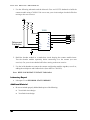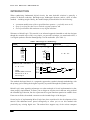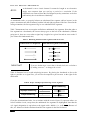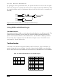
1
SCHOOL OF ELECTRICAL AND COMPUTER ENGINEERING
Georgia Institute of Technology
Digital Hardware
Design Laboratory
Fall 1999
Michael D. Furman and Tyson S. Hall
All Rights Reserved, Copyright © 1999, M. D. Furman
D I G I T A L
D E S I G N
L A B O R A T O R Y
Table of Contents
INTRODUCTION & SYLLABUS ..................................................................... ii
LAB 1:
SIMULATION AND HARDWARE ....................................................... 1
LAB 2:
SIMPLE STATE MACHINES – SYNTHESIS ......................................... 3
LAB 3:
SIMPLE STATE MACHINES – DISCRETE & VHDL MODELING ............ 5
LAB 4:
CIRCUIT CHARACTERISTICS & OSCILLOSCOPES ............................. 6
LAB 5:
DISCRETE CIRCUIT DESIGN .......................................................... 9
LAB 6:
DISCRETE CIRCUIT ANALYSIS & LOGIC ANALYZERS ...................... 11
LAB 7:
TRAIN SIMULATION ..................................................................... 12
LAB 8:
COMPUTER I: INSTRUCTION SET ARCHITECTURE ........................... 15
LAB 9:
COMPUTER II: DATAPATH & CONTROL ......................................... 16
LAB 10: COMPUTER III: RANDOM ACCESS MEMORY ................................... 17
LAB 11: ROBOTICS: OBSTACLE AVOIDANCE & COMPASS ............................ 18
LAB 12: ROBOT CHALLENGE: A TEAM DESIGN PROJECT ............................ 19
APPENDIX A: LOGIC ANALYZER TUTORIAL .............................................. A.1
APPENDIX B: FUNDAMENTAL DIGITAL DESIGN USING MIXED LOGIC .......... B.1
APPENDIX C: USING ASM CHARTS FOR STATE MACHINE DESIGN .............. C.1
i
D I G I T A L
D E S I G N
L A B O R A T O R Y
Read Before Coming to Lab
Welcome to the digital hardware design laboratory. This book is a supplement to the
textbook and is designed to give specific instructions for ECE 2031. Tutorials are included
(or will be handed out in class) to demonstrate mixed logic, the oscilloscope, the logic
analyzer, writing reports, and state machine designs. The student is required to read the
laboratory and perform any Prelab exercises before coming to the lab, since most exercises
will consume the full three-hour lab session.
The laboratory assumes an in-lab setup of a computer-based digital simulation package, an
oscilloscope, a logic analyzer, and Altera's UP 1 university board, a CADET II digital
design station, and the miscellaneous items listed below.
You will need to have with you the following supplies before you come to lab:
!" Rapid Prototyping of Digital Systems by James O. Hamblen and Michael D.
Furman.
!" This lab manual.
!" The Wire Kit – The wires in this kit are pre-stripped and pre-bent for easy
insertion into the protoboard.
!" 2 – 3.5" Floppy Disks – Label these with your name and lab section.
!" The Fast and LS TTL Data Manual – This is provided by Motorola and may be
picked up in the lab.
!" ECE NT Account. To activate your account see a UA in one of the ECE NT
labs (3rd floor CoC). You must have this account before coming to the first
lab.
ii
D I G I T A L
D E S I G N
L A B O R A T O R Y
Online Resources
The Digital Laboratory Web Page is located at:
http://www.ece.gatech.edu/research/labs/diglab
This page is under constant development and represents the latest changes in the lab
manual, chip prices, downloadable report templates, software, and video tutorials. There are
also current lab hours (including weekend hours), teaching assistant names, pictures, and
email addresses.
Lab Logistics
Some of your key responsibilities for this lab are as specified under the following topics.
Please read carefully.
Texts
Two texts will be used for this lab. The textbook is Rapid Prototyping of Digital Systems by
James O. Hamblen and Michael D. Furman (hereafter referred to as the textbook). The
second text is this lab manual (hereafter referred to as the lab manual).
Lab Quizzes
A lab quiz will be given at the beginning of each lab. They will be designed to test your
general understanding of what is about to be done in the lab. Reading over the lab and
attending lectures will generally be sufficient preparation for the quiz. (The quizzes may be
moved to the lecture section of the course. You will be informed if this is the case.)
Mid-Term
A short mid-term exam will be given during week 7 of the quarter (tentatively scheduled on
October 8, 1999). It will cover the material in both the lectures and the labs and will last the
full lecture period.
Final Exam
A final exam will be given during the lab period in dead week (December 6-10). This exam
will contain both a written and practical part designed to test the students’ knowledge of the
concepts covered in the lectures and labs.
iii
D I G I T A L
D E S I G N
L A B O R A T O R Y
Grades
A final grade will be assigned based on the following submitted work.
30% - Lab Reports
30% - Final
20% - Prelab Quizzes
10% - Midterm
10% - TA Perspective
Circuit Diagrams
For labs requiring them, a computer-generated circuit diagram and simulation must be
completed before building the hardware circuit. This will help the student both debug the
circuit and insure that he/she starts with a workable design.
!" Make sure that your name and date are on the circuit diagram in the format of
the software package. Diagrams with other formats will be invalid.
!" Layout diagram left to right. See the examples in lab.
MAX+PLUS II Timing Diagrams
Label all timing diagrams correctly. (See Report Format on the web site for proper figure
captions.) Note: It should have signals in an order indicated by the design and should be
illustrated in a format that adds understanding to the report. (i.e., inputs and outputs should
be in the same order as illustrated in the truth table. Signals should be in a logical
numerical increasing order.)
Maintain the Sign-Off Sheet
The instructing TA must verify all performed labs. This requires a signature on the "signoff" sheet. This sign-off sheet is to be turned in with the lab report.
Announcements
With this being a new course, changes will be inevitable. You are responsible for all
announcements made in lecture or lab and all material written on the board in the lab or
emailed to the class during the course of the quarter. Changes and modifications will be
made via one or more of these mediums.
iv
D I G I T A L
D E S I G N
L A B O R A T O R Y
Using Your ECE Home Directory
!" With each ECE NT account, you are allotted 20 MB of server disk space.
!" When you logon to any NT machine in the ECE computer labs (Van Leer C252, E283,
and CoC 3rd floor), a drive is automatically mapped to your individual directory. In the
Digital Lab, this is drive Z, and it is a great way to keep a backup of your ECE 2031
work. You can use drive Z just as you use floppy drive A.
!" Due to the volume of network traffic it is best to work on the local drive. Create a
temporary directory on C and use it while you're working in the lab. Before you leave,
be sure to MOVE YOUR DIRECTORY TO DRIVE Z. Machines will be refreshed daily
and all work left on local hard drives will be deleted!
!" Due to the 20 MB limit, it would be wise to zip your working directory when the lab is
over and only store the zipped file.
!" If you do use the network drive be aware that you must work within a subdirectory while
using MAX+PLUS II. Use of the "root" Z directory will cause problems when
compiling.
Penalty Points
5-Point Penalties
!" Leaving trash in the work area.
!" Unauthorized tampering with the lab facilities and/or computer equipment.
10-Point Penalties
!" For each day a lab report is late. Students' check-off sheets must be signed by a TA at
least two days prior to the submission of the corresponding report due date.
Other
!" Students must remain in the lab during the three-hour period or until the lab is complete.
Students will be accessed proportionately for arriving late or leaving early.
!" Failure to have your work checked-off by the teaching assistant will result in an F being
assigned to the current lab assignment.
v
D I G I T A L
D E S I G N
L A B O R A T O R Y
!" Failure to turn in a lab assignment will result in an F being assigned to the final grade.
No lab will be accepted two weeks after the due date.
!" There will be no make-up quizzes. No exceptions. You will be granted one drop to take
care of potential excused absences (i.e., sickness, plant trips, death in the family, etc.).
Honor Violations
!" Cheating of any kind will not be tolerated. The Honor Code is strictly enforced.
!" Students should be prepared to provide an electronic copy of their work (all schematics,
source code, and reports) upon request. Failure to do so will be handled as an honor
violation.
!" Never leave any work, schematics, and/or timing diagrams on the hard disk of any
computer located in the lab. See Using Your ECE Home Directory for one of your
permanent storage options.
Acknowledgements
Many people helped make this laboratory manual possible. We would particularly like to
express our appreciation to the students who suggested corrections and helped to weed out
the problem exercises. We would also like to thank those graduate and undergraduate
teaching assistants that made countless modifications and improvements on the various
tutorials.
vi
D I G I T A L
D E S I G N
L A B O R A T O R Y
Schedule (Tentative)
Week
1
2
3
4
5
6
7
8
9
10
11
12
13
14
15
Dates
Lab #
8/27
8/31-9/1
9/3
9/7-9/8
9/10
9/14-9/15
9/17
9/21-9/22
9/24
9/28-9/29
10/1
10/5-10/6
10/8
10/12-10/13
10/15
10/19-10/20
10/22
10/26-10/27
10/29
11/2-11/3
11/5
11/9-11/10
11/12
11/16-11/17
11/19
11/23-11-24
11/26
11/30-12/1
12/3
12/7-12/8
1
2
3
4
5
6
7
8
9
10
11
12
12
Subject
Report Type
Intro/Syllabus/Writing Reqs.
Simulation and Hardware
Informal Status
Mixed Logic/State Machines
Simple State Machine - Synthesis
Informal Report
VHDL-I: Entity/Process/Simple Gates
Simple State Machine – Discrete & VHDL Informal Status
Oscilloscope Demo/Intro. To Timing
Circuit Characteristics & Oscilloscopes
Formal Report
VHDL-II: State M. & Adv Topics in VHDL
Discrete Circuit Design
Informal Status
Intro to Train/Logic Analyzer Demo
Discrete Circ. Analysis & Logic Analyzer Informal Report
Mid-Term Exam
Train Lab
Informal Report
Computer: Top Down Design, MUXs
<Mid-Term Recess>
Computer: VHDL Implementation
Computer: Instruction Set Arch.
Informal Status
Computer: Adders, ALUs
Computer: Datapath & Control
Informal Status
Timing Diagram to State Machine
Computer: RAM
Formal
Intro to UP1bot
Robot: Avoidance & Compass
Informal Status
Project Planning/Writing a Group Report
Robot Challenge: Team Design Project
Informal Status
<Thanksgiving Break>
Robot Challenge: Team Design Project
Formal
Review for Final Exam
Final Exam (during regular lab period)
Legend
Bold = Laboratory
Italics = Lecture
August
Sunday
Monday
22
Tuesday
23
Wednesday
24
Thursday
25
Friday
26
Saturday
27
28
3
4
Lect: Introduction
29
30
31
Lab 1: Altera Tutorials 1 & 2, 2 days
1
2
Lect: Mixed Logic
vii
D I G I T A L
D E S I G N
L A B O R A T O R Y
September
Sunday
Monday
29
Tuesday
30
Wednesday
Thursday
31
1
Friday
2
Lab 1: Altera Tutorials 1 & 2, 2 days
5
6
7
8
9
Lab 2: Simple State Machine - Design & Simulation,
12
13
14
20
15
21
16
27
22
28
10
11
17
18
24
25
1
2
Lect: Oscilloscope
23
Lab 4: Circuit Characteristics & Oscilloscopes, 2 day
26
4
Lect: VHDL I
Lab 3: Simple State Machine - Discrete & VHDL, 2 d
19
Saturday
3
Lect: Mixed Logic
Lect: VHDL II
29
30
Lab 5: Discrete Circuits, 2 days
Lect: Intro to Train
October
Sunday
Monday
26
Tuesday
27
Wednesday
28
Thursday
29
Friday
30
Lab 5: Discrete Circuits, 2 days
3
4
5
6
7
Lab 6: Discrete Circuit Analysis & Logic Analyzer, 2 d
10
11
12
Saturday
1
2
8
9
15
16
22
23
29
30
Lect: Intro to Train
13
Mid-Term Exam
14
Lab 7: Train Lab, 2 days
Lect: Simple Comp
Drop Day
17
18
19
20
21
Mid-Term Break, 2 days
24
25
Lect: Simple Comp
26
27
Lab 8: Computer: Instruction set Architecture, 2 days
viii
28
Lect: Simple Comp
D I G I T A L
D E S I G N
L A B O R A T O R Y
November
Sunday
Monday
31
Tuesday
1
Wednesday
2
Thursday
3
Friday
4
Lab 9: Computer: Datapath & Control, 2 days
7
8
9
10
11
Lab 10: Computer: Ram, 2 days
14
15
16
22
17
23
29
18
24
30
12
13
19
20
26
27
3
4
Lect: Project Plan
Lab 12: Team Design Project: Robot Challenge, 2 da
28
6
Lect: Intro UP1-bot
Lab 11:Robot: Avoidance, Compass, 2 days
21
Saturday
5
Lect: Timing State
25
Thanksgiving Holiday, 2 days
1
2
Lab 12 Cont.: Team Design Project: Robot Challenge
Lect: Rev. for Final
December
Sunday
Monday
28
Tuesday
29
Wednesday
30
Thursday
1
Friday
2
Lab 12 Cont.: Team Design Project: Robot Challenge
5
6
7
Saturday
3
4
Lect: Rev. for Final
8
9
10
11
In-Lab Exam, 2 days
12
13
14
15
16
17
18
19
20
21
22
23
24
25
26
27
28
29
30
31
1
ix
D I G I T A L
D E S I G N
L A B O R A T O R Y
Taking Quizzes with WebCT
!" Use Netscape or IE to go to webct.gatech.edu.
!" Click on Access Courses in the upper left-hand corner.
!" Click on ECE (Electrical and Computer Engineering).
!" Click on ECE2031L1-L6: Digital Hardware Laboratory.
!" Enter your gt# (in lower case) for the User Name and the last 4 digits of your social
security number for the Password.
!" Click on Fall Quizzes.
!" Click on the day of the week that your lab section meets (i.e. Tuesday).
!" Click on the time of day that your lab section meets (i.e. 12-3).
!" Click on the appropriate quiz name (i.e. Quiz One).
!" Each quiz is password protected. Ask your TA for the password for the quiz you are
starting.
Note: The system makes quizzes available only during the first half hour of your lab
section. If you are late, there is no make-up quiz. Also, once you start the quiz, you will
have 15 minutes to complete it before WebCT disconnects you and grades your quiz “as is.”
x
D I G I T A L
D E S I G N
L A B O R A T O R Y
1
Laboratory
Simulation and Hardware
This lab is designed to acclimate the student to the Altera MAX+PLUS II CAD software and
introduce the techniques used to design, compile, simulate, and implement digital hardware
in a CPLD environment. Using two tutorials, the student is introduced to the schematic
capture, VHDL capture, simulation, and download capabilities of the Altera development
system.
Prelab Exercises
!" Look over Chapters 1 and 4 of the textbook. Since these are tutorials, you do not need to
read them before coming to lab.
!" Read class handout on writing. You will need to understand what to report before you
start the lab.
Laboratory Exercises
1. Perform all steps in Chapter 1 of the textbook.
2. Complete Laboratory Exercises 1 and 2 at the end of Chapter 1.
3. Perform all steps in Chapter 4 of the textbook.
4. Complete Laboratory Exercises 2 and 3 at the end of Chapter 4.
!"Bonus: Complete Laboratory Exercise 4 at the end of Chapter 4.
1
D I G I T A L
D E S I G N
L A B O R A T O R Y
Laboratory Report
!" Lab report 1 is an INFORMAL STATUS REPORT.
!" Be sure to include properly labeled hard copies of the following:
#"
Schematic, VHDL code, and simulation waveform for Chapter 1 (OR gate).
#"
Schematic, VHDL code, and simulation waveform for Exercises 1.1 and 1.2
(AND gate).
#"
Schematic for Exercise 4.2.
#"
Schematic for Exercise 4.3.
#"
Schematic for Exercise 4.4 (optional).
Additional Material
!" Mixed Logic Tutorial (Appendix B)
2
D I G I T A L
D E S I G N
L A B O R A T O R Y
2
Laboratory
Laboratory
Simple State Machines – Synthesis
This lab is designed to familiarize the student with the design, simulation, and synthesis of
state machines using Altera MAX+PLUS II and the UP 1 development board.
Prelab Exercises
!" Review state machines from your ECE 2030 notes.
Laboratory Exercises
1. Demonstrate the operation of a D flip-flop by completing Exercise 16 at the end of
Chapter 1.
2. A D flip-flop can be configured to output a square wave on Q that is half the frequency
of the flip-flop's clock. Demonstrate (with a simulation waveform) the operation of this
"divide-by-two" circuit. Hint: You will need a clock input, but you will not need any
other external inputs.
3.
Complete Laboratory Exercise 18 at the end of Chapter 1, but use the state machine
diagram given below.
3
D I G I T A L
D E S I G N
L A B O R A T O R Y
Reset
A
0X
1X
0X
11
B
C
Output 1
10
Laboratory Report
!" Lab report 2 is an INFORMAL REPORT.
!" Be sure to include properly labeled hard copies of the following:
#"
An annotated simulation waveform of the D flip-flop. Include a description of a
D flip-flop's functionality.
#"
Schematic and simulation waveform for the divide-by-two circuit.
#"
Schematic and simulation waveform for Exercise 1.18 (state machine).
Additional Material
!" Latches and Flip-Flops Tutorial (lecture handout)
4
D I G I T A L
D E S I G N
L A B O R A T O R Y
3
Laboratory
Simple State Machines – Discrete & VHDL
Modeling
This lab is designed to familiarize the student with discrete digital design, protoboards, and
discrete and VHDL state machines.
Prelab Exercises
!" Review state machines from your ECE 2030 notes.
!" Read Chapter 6 of the textbook.
Laboratory Exercises
1. Build and test the state machine designed in lab 2 using discrete gates. A video
demonstration on the use of the protoboards is available online. See your teaching
assistant for more information on its location. Save your circuit for use in lab 4.
2. Complete Laboratory Exercise 2 at the end of Chapter 6 using the state machine from
lab 2.
Laboratory Report
!" Lab report 3 is an INFORMAL STATUS REPORT.
!"
Be sure to include properly labeled hard copies of the following:
#"
Schematic and simulation waveform for the state machine.
#"
VHDL code and simulation waveform for Exercise 6.2 (state machine).
Additional Material
!" Online video demonstration on using a protoboard.
!" A VHDL quick reference guide is available from the lab by going to Start -> Run and
then typing \\POMPEII\diglab\help.
5
D I G I T A L
D E S I G N
L A B O R A T O R Y
4
Laboratory
Circuit Characteristics & Oscilloscopes
This lab is designed to introduce students to basic circuit characteristics, measurement
techniques, and the oscilloscope.
Prelab Exercises
!" N/A
Laboratory Exercises
1. Hook up two D flip-flops (one 7474 or equivalent) in a divide-by-four configuration as
illustrated below. Set the clock to approximately 1 KHz.
All PRN and CLRN signals tied to HIGH.
exp
dff
PRN
D
7
Clock
INPUT
VCC
exp
dff
PRN
Q
D
/Q
Div_by_2
OUTPUT
10
Div_by_4
Q
/Q
CLRN
6
OUTPUT
9
CLRN
8
If you could see all three signals on the scope, they would look something like the
following timing diagram. Ultimately, you will be measuring the propagation delay as
indicated by the arrows.
Clock
Div_by_2
Div_by_4
6
D I G I T A L
D E S I G N
L A B O R A T O R Y
2. First, with the oscilloscope, measure the characteristics in the table. Take screen
captures (HardCopy) of the Rise and Fall Time screens to include in your report. Be
prepared to describe why there are changes between the signals in your report.
Signal
Period
Frequency
Rise Time
Fall Time
Positive
Duty Cycle
Peak-toPeak
Clock
Div_by_2
Div_by_4
3. Place the clock on Channel 1 and Div_by_4 on Channel 2. Using the cursors, measure
the propagation delay. This measurement should be taken from the half-voltage points of
each curve as illustrated below.
Ch1
Ch2
4. Hook up the MAX_PB1 pushbutton on the UP 1 board to Channel 1 of the oscilloscope.
Connect pin 32 on the MAX chip to the ground on the oscilloscope’s probe. Press the
pushbutton and observe the “bouncing” effect as illustrated in Figure 4.7 of the
textbook. How would you eliminate the keybounce if you were to use a pushbutton in
one of your circuits?
5. Use the oscilloscope to measure the maximum propagation delay of your state machine
circuit from lab 3.
7
D I G I T A L
D E S I G N
L A B O R A T O R Y
Laboratory Report
!" Lab report 4 is a FORMAL REPORT. It should cover the material from labs 2, 3,
and 4.
!" Be sure to include properly labeled hard copies of the following:
#"
Appropriate material from Chapters 2 and 3.
#"
Oscilloscope screen captures and measurements taken in lab 4.
#"
Schematic for the state machine with the maximum propagation delay path
marked.
Additional Material
!" Oscilloscope in-class demonstration.
8
D I G I T A L
D E S I G N
L A B O R A T O R Y
5
Laboratory
Discrete Circuit Design
This lab is designed to familiarize the student with discrete digital design. The student is
introduced to discrete counters, decoders, and multiplexers.
Prelab Exercises
!" Use MAX+PLUS II to design a preliminary schematic BEFORE coming to lab.
Laboratory Exercises
These exercises will step you through designing a counter that counts 0, 1, 2, …, x, 0, 1, …
or 0, 1, 2, …, y, 0, 1, … depending on whether a switch is on or off. The values of x and y
will be given to you during your lab period. The following diagram is an overview of the
components that you will design.
7-Seg.
Display
Clock
Counter
Decoder
MUX
Switch
9
D I G I T A L
D E S I G N
L A B O R A T O R Y
1. Use the following schematic and the Motorola Fast and LS TTL databook to build the
counter module using a 74LS193. Be sure to test your circuit and get checked off before
moving to the next exercise.
74193
PL
Debounced
Pushbutton
P0
Q0
P1
Q1
P2
Q2
P3
Q3
CPD
TCU
CPU
TCD
LED1
LED2
LED3
LED4
MR
COUNTER
2. Build the decoder module as a stand-alone circuit keeping the counter module intact.
Test the decoder module separately before connecting it to the counter (see next
exercise). Get your circuit checked off before moving to the next exercise.
3. Use the in-lab handout to connect the counter and decoder modules together, as well as,
adding the multiplexer and feedback wire (from MUX to 74LS193).
Note: KEEP YOUR CIRCUIT INTACT FOR LAB 6.
Laboratory Report
!" Lab report 5 is an INFORMAL STATUS REPORT.
Additional Material
!" Be sure to include properly labeled hard copies of the following:
10
#"
Your initial circuit design.
#"
Your final circuit design.
D I G I T A L
D E S I G N
L A B O R A T O R Y
6
Laboratory
Discrete Circuit Analysis & Logic Analyzers
This lab is designed to introduce students to circuit analysis, debugging techniques, and the
logic analyzer.
Prelab Exercises
!" Review the logic analyzer tutorial (Appendix A).
Laboratory Exercises
1. Using the oscilloscope, measure the nominal propagation delay of the counter circuit
you built in lab 5. In this case, the nominal propagation delay is the time between the
pushbutton being released and the new value (except zero) reaching the seven-segment
display.
2. Using the oscilloscope, measure the maximum propagation delay of the counter circuit
you built in lab 5. In this case, the maximum propagation delay is the time between the
pushbutton being released when the counter is at its largest count value and the new
value (zero) reaching the seven-segment display.
3.
Using the logic analyzer repeat exercises 1 and 2. Compare your results in your report.
Laboratory Report
!" Lab report 6 is an INFORMAL REPORT. It should cover the material from lab 5
and lab 6.
!" Be sure to include properly labeled hard copies of the following:
#"
Schematics from lab 5.
#"
Screen captures for the measurements made with the oscilloscope.
#"
Annotated timing diagram from the logic analyzer. Be sure to show where you
take your propagation delay measurements.
Additional Material
!" Logic Analyzer Tutorial (See Appendix A of this lab manual.)
11
D I G I T A L
D E S I G N
L A B O R A T O R Y
7
Laboratory
Train Simulation
This lab is designed to give the student experience working with more advanced state
machines and more complex VHDL code. Teamwork is encouraged as students may
complete this lab in groups of two.
Prelab Exercises
!" Thoroughly read Chapter 7 of the textbook BEFORE coming to lecture.
!" With your partner, design the state machine BEFORE coming to lab.
Laboratory Exercises
4. Complete lessons 1-6 of the MasterClass Lite VHDL Tutorial (see next page for
installation instructions). This should take a little over 2 hours to finish if you listen to
the narrator. It can be completed in less time if you read it.
5. In groups of two, complete Laboratory Exercise 2 at the end of Chapter 7.
Laboratory Report
!" Lab report 7 is an INFORMAL REPORT.
!" Be sure to include properly labeled hard copies of the following:
#"
A state diagram for your new train controller.
#"
The VHDL code for your new train controller.
!" INDIVIDUAL reports are required.
Additional Material
!" Software documentation, VHDL syntax, and component behavioral descriptions are
available from the Help menu in MAX+PLUS II.
!" A VHDL quick reference guide is available from the lab by going to Start -> Run and
then typing \\POMPEII\diglab\help.
12
D I G I T A L
D E S I G N
L A B O R A T O R Y
Installing the Tutorial
!" Check out a MasterClass Lite CD-ROM from the TA and insert it in the CD-ROM drive.
!" Go to Start -> Run, and type E:\mcvhdl\program\setup.exe
!" Click OK to continue.
!" Click Continue on the next two screens. If it prompts you to verify overwriting of
existing files, click No to avoid getting more messages.
!" When the installation is complete, click the OK button.
Running the Tutorial
!" To maximize the viewing screen, you can set the screen resolution to 640 x 480 by going
to Start -> Settings -> Control Panel -> Display -> Settings and changing the Desktop
Area parameter.
!" Also, the sound may be muted on your computer. To correct this, double click on the
yellow speaker on the bottom right-hand corner of the desktop
all the Mute boxes that are checked.
. Click on
!" Double click on the MasterClass 2.0 icon. The following screen should be displayed
!" Clicking on the Tutorial button brings up the Contents window (see below).
13
D I G I T A L
D E S I G N
L A B O R A T O R Y
Click
here
Click
here first
!" The Contents window allows you to navigate through the tutorial. Click on the
desired lesson in the left-hand window, and then click on the first topic (i.e., 1-1) in
the right-hand window.
!" When lesson 1 starts, click on the navigational buttons with diagonal red lines (as
shown below) to turn on the sound and automation features. Now, sit back and enjoy
the presentation.
Click on each of these
buttons to enable sound
and automation.
14
Use these buttons to
navigate through the
tutorial.
D I G I T A L
D E S I G N
L A B O R A T O R Y
8
Laboratory
Computer I: Instruction Set Architecture
This lab is designed to introduce the student to the basic VHDL modeling of the instruction
set of a simple computer.
Prelab Exercises
!" Read Chapter 8 in the textbook.
Laboratory Exercises
1. Complete Laboratory Exercise 1 at the end of Chapter 8.
2. Complete Laboratory Exercise 2 at the end of Chapter 8.
3. Complete Laboratory Exercise 3 at the end of Chapter 8.
Laboratory Report
!" Lab report 8 is an INFORMAL STATUS REPORT.
!" Be sure to include the following:
#"
Simulation waveform and your new program.mif file from Exercise 8.1.
#"
Answers to all the questions asked in Exercise 8.1.
#"
VHDL code for your new CASE statement, simulation waveform, and your new
program.mif file from Exercise 8.2.
#"
VHDL code for your new instructions, simulation waveform, and the test file you
created to test them from Exercise 8.3.
Additional Material
!" Software documentation, VHDL syntax, and component behavioral descriptions are
available from the Help menu in MAX+PLUS II.
!" A VHDL quick reference guide is available from the lab by going to Start -> Run and
then typing \\POMPEII\diglab\help.
15
D I G I T A L
D E S I G N
L A B O R A T O R Y
9
Laboratory
Computer II: Datapath & Control
This lab is designed to introduce the student to the datapath and control of a simple
computer. It is a continuation of lab 8.
Prelab Exercises
!" Review Chapter 8 of the textbook.
Laboratory Exercises
1. Complete Laboratory Exercise 5 at the end of Chapter 8. Use the programs written for
Exercises 8.2 and 8.3. Verify that their behavior matches the simulations you made in
lab 8.
2. Complete Laboratory Exercise 6 at the end of Chapter 8.
3. Illustrate the simple computer's datapath by tracing the execution of the program from
Exercise 8.2. Use an ASM-type chart like the one in Figure 8.6. Your chart will have
only one path, because you are mapping a specific thread of execution.
Laboratory Report
!" Lab report 9 is an INFORMAL STATUS REPORT.
!" Be sure to include properly labeled hard copies of the following:
16
#"
Simulation waveform and your test file from Exercise 8.6.
#"
A chart showing the thread of execution for Exercise 8.2 (number 3 above).
D I G I T A L
D E S I G N
L A B O R A T O R Y
10
Laboratory
Computer III: Random Access Memory
This lab is designed to introduce the student to the data and instruction memories of a
simple computer and MAX+PLUS II's memory synthesis capabilities. It is a continuation of
lab 8 and lab 9.
Prelab Exercises
!" Read Section 6.14 of the textbook. This covers memory synthesis.
Laboratory Exercises
1. Complete Laboratory Exercise 11 at the end of Chapter 8.
2. Complete Laboratory Exercise 12 at the end of Chapter 8.
Laboratory Report
!" Lab report 10 is a FORMAL REPORT. It should cover the material from lab 8, lab
9, and lab 10.
!" Be sure to include properly labeled hard copies of the following:
#"
All figures and tables from lab 8 and lab 9.
#"
Modified VHDL code from Exercise 8.11 and 8.12. Note: In a formal report it is
best to include relevant samples of the VHDL code in figures as you discuss them
and then include the entire VHDL code as an appendix. When properly done, this
adds to the flow of the report.
Additional Material
!" Section 6.14 of the textbook covers memory synthesis in VHDL.
17
D I G I T A L
D E S I G N
L A B O R A T O R Y
11
Laboratory
Robotics: Obstacle Avoidance & Compass
This lab is designed to introduce the student to the UP1-bot and give him/her experience
designing, modifying, and debugging a state machine that controls mechanical devices.
Teamwork is encouraged as students may complete this lab in groups of two.
Prelab Exercises
!" Chapter 12: read Sections 12.1, 12.4, and 12.5 (sensors, IR proximity detector, magnetic
compass). Other sections are for your edification only.
Laboratory Exercises
In groups of two:
1. Complete Laboratory Exercise 15 at the end of Chapter 12.
2. Form a group for the final design project and begin working (see lab 12).
Laboratory Report
!" Lab report 11 is an INFORMAL STATUS REPORT.
!" Be sure to include properly labeled hard copies of the following:
#"
A state diagram and VHDL code for your UP1-bot controller from Exercise
12.15.
Additional Material
!" Software documentation, VHDL syntax, and component behavioral descriptions are
available from the Help menu in MAX+PLUS II.
!" A VHDL quick reference guide is available from the lab by going to Start -> Run and
then typing \\POMPEII\diglab\help.
18
D I G I T A L
D E S I G N
L A B O R A T O R Y
12
Laboratory
Robot Challenge: A Team Design Project
This lab is designed to give the student experience working in a team environment to
complete an extended design project. The rest of the term will be given to complete this
project, and a formal group report is required. Teams of four are allowed for this project.
Laboratory Exercises
Design a state machine to control the UP1-bots in a Q-zar-type laser tag competition.
Robots on a given team will need to work together. They will be able to detect friend or foe
in a forward direction along with the compass and avoidance capabilities of the previous
labs. Additionally, your robots will have the ability to fire a small laser with the duration of
0.5 seconds every 5 seconds. If a robot is hit, it will be incapacitated for a period of 5
seconds. Your robots will run for a specified time limit. Your task is to survive.
A competition between robot teams will be held at the end of the term.
More information will be supplied as the limitations of the robots are established.
Laboratory Report
!" Lab report 12 is an INFORMAL STATUS REPORT. It is due at the next lab
meeting. One report per group is required. Each group member will get the same
grade on the report.
!" Lab report 13 is a FORMAL REPORT. One report per group is required. Each
group member will get the same grade on the report.
!" Each group member is required to complete a peer survey for everyone else in his/her
group.
!" Be sure to include properly labeled hard copies of the following:
#"
Top-level schematic of your UP1-bot.
#"
Schematics and/or VHDL code for every component you modified or created for
this project. Note: In a formal report it is best to include relative samples of the
VHDL code in figures as you discuss them and then include the entire VHDL
code as an appendix. When properly done, this adds to the flow of the report.
#"
A state diagram for your UP1-bot controller.
19
D I G I T A L
D E S I G N
L A B O R A T O R Y
A
Appendix
Tektronix TLA 704 Logic Analyzer
This tutorial is designed to acclimate the student to the Tektronix TLA 704 Logic Analyzer. It
is not meant to supply all of the details on how to use the logic analyzer. The tutorial will use
the "Teaching by an Example" approach.
If additional information is needed, see the Help topics in the analyzer software
or the TLA 700 Series User Manual (part # 070-9775-01).
L
ogic analyzers are common analysis tools in the digital engineering environment.
Students who want jobs in electronics will inevitably have to use logic analyzers
throughout their career. To understand how to use them, it is helpful to know the basics of
how they work.
Logic analyzers are similar to digital oscilloscopes in many ways; however they are
generally used when it is less important to measure the actual voltage of a particular signal.
With the exception of some newer, very expensive, digital models, most oscilloscopes need
repetitive signals to trigger. Logic analyzers can be used to analyze the timing between
digital signals even when the signals are not repetitive.
Since glitches in a system are generally non-repetitive and can cause major problems, the
wise engineer can use the logic analyzer to track down such problems. This can be
accomplished by setting the triggering system of the analyzer to trigger on such glitches.
The Basics
Logic analyzers monitor an input signal to see if it is above or below some threshold
voltage. If the voltage is above the threshold, it is converted to a 1; if the voltage is below
the threshold, it is converted to a 0. A sampling clock triggers the analyzer to sample the
1’s and 0’s at a particular rate. When sampled, the 1 or 0 is stored in memory. After filling
the memory, the analyzer can use the stored values to create a waveform that represents the
sampled input.
A.1
A.1
D I G I T A L
D E S I G N
L A B O R A T O R Y
The accuracy of the displayed waveform depends on the sampling clock frequency. The
higher the frequency of the sampling clock, the more accurately the input can be
represented.
In engineering, when making something better, there is almost always a trade-off. Since the
logic analyzer has a limited amount of memory for storing information, the trade-off for
higher sampling clock rates is the reduced time window of input data that can be stored. For
example, pretend that the output of a counter was being analyzed at a sampling clock period
of 10ns (100 MHz) and the entire sequence of the counter exactly filled the memory.
Changing the sampling clock period to 5ns (200 MHz) will cause the memory to become
full after half as much time.
The TLA 704 Computer
The TLA 704, as you see it, is truly a computer that comes standard with a 1.4 gigabyte
hard drive, 16 megabytes of DRAM, a dual scan LCD display similar to most laptops, a
NMB keyboard, and a Logitech mouse. The operating system is Microsoft’s Windows 95.
The control panel, on the front of the TLA 704, provides a method of controlling the device
in case the mouse or keyboard is not available. The little square with the mouse on it, in the
upper-right corner is a static pad that gives most of the functions of a regular mouse, even
double-clicking by tapping your finger.
The computer has additional ports for connecting an external monitor, a serial (RS-232)
device, a PC card, or a printer. The printer port requires the enhanced parallel port cable
(EPP), which comes with the device, to connect to a stand-alone printer. With the serial port
or the PC card slot, the computer can be connected to a network via modem or a network
card.
The TLA 704 Analyzer
The logic analyzer is actually a plug-in module that rests in two of the four module
expansion slots on the right side of the computer. The analyzer has four probe ports, each
having eight probes: A2(7-0), A3(7-0), C2(7-0), and C3(7-0). Ignore the CK0 and CK3 for
now.
Groups are generally formed from the probes to provide better information. A group is
made up of one or more probe channels and is generally given a descriptive name, i.e. the
outputs of a counter could be grouped together under the name "Outputs" and then
displayed individually or as one vector that shows the number of the current count. Each
probe channel can be in a group by itself or can be in as many groups as the user would
like. This makes it possible to define an almost unlimited number of groups.
A.2
A.2
D I G I T A L
D E S I G N
L A B O R A T O R Y
The TLA 704 Software
The logic analyzer software should be very intuitive to any one who is familiar with the
Windows 95 environment and has some clue as to what they want to do. Each window
provides help through pressing F1 or through clicking on the Help button.
The Example
The example assumes that the probes are connected to the logic analyzer and are
secured with the mounting hardware to prevent them from accidentally coming loose.
If this is not the case, get a QUALIFIED person to do this.
!" Keep in mind that the Tek 704 is a costly, state-of-the-art piece of test
equipment. Please treat it as such.
!" Assemble the circuit that will be analyzed.
!" Turn on the computer and wait for it to finish the start-up procedure.
!" If the Window’s 95 "tip of the day" is visible, close it.
!" The logic analyzer software should start up on its on. If not, start it by doubleclicking the TLA 700 Application icon.
!" Connecting the probes and other Setup window items.
Mini-Grabbers
Always use the probe connector tips (mini-grabbers) that the probe point can plug
into. DO NOT plug wire into the end of the probe point. This can damage the plug
and/or the wire could break off in the plug.
!" Connect the middle probe (solid black cover) to ground.
!" With the power to your circuit OFF, decide which probes to use (and which
groups to create with the probes, if any), then connect them to the circuit.
In the TLA 700 System window, there should be a System window that has at least 3
clickable buttons: On/Off, Setup, and Trig.
!" Click Setup to go to the Setup window.
!" Replace the current Group Names with ones appropriate to your circuit. For the
counter circuit, you'll want groups like "Clock", "Clear", "Outputs", etc. You
should also add any other signals that you need to properly take the required
measurements. Groups are analogous to buses or vectors.
A.3
A.3
D I G I T A L
D E S I G N
L A B O R A T O R Y
Naming
A2(5-0) probes will be used, therefore, name the probes by clicking in the area to the right
of each in the Probe Names/Channels box. This is where you name each individual signal
and assign it to a specific probe. It would be helpful to use the same names you used in
Altera (i.e. "Clock", "LED1", "LED2", etc). Generally, if a group has only one channel in it,
naming the group and the probe channel the same name makes life easier.
The Clock
To add the "Clock" probe to the "Clock" group, click in the area adjacent to the group name
"Clock", under MSB Probe Channels LSB, then click the box in the Probe Names/Channels
area that you assigned to "Clock." An X should appear and the probe should be added to the
group.
Add the other probes to their appropriate group in the same manner. When adding the
outputs, keep in mind that they should be added in the order of MSB to LSB. This will
allow the vector representation of the output to be correct.
Be sure that Clocking is set to Internal and Acquire is set to Normal.
Clock Period
Determine the logic analyzer’s sampling clock period. The maximum memory size is
32768, so if the period of "Clock" is 1 ms (1 KHz), the minimum sampling clock period is
given by: sampling clock = ( circuit clock period / 32768 ) * acquired circuit clock cycles
desired -> ( 1ms / 32768 ) * 15 = 458 ns. (The 15 is used because we want to be sure and
see a full loop of the counter.) Pick the next highest value of sampling clock period, which
would be 500 ns.
Memory Depth and Threshold
Set Memory Depth to its highest possible value -> 32768.
The Set Threshold button allows the user to change the voltage thresholds that were
described earlier. We will assume that they are set correctly, but you can check this as a
debug step if the waveforms do not appear to be correct. Use the default TTL settings for
all 74LS parts.
Trigger Event
Setting up the trigger is optional for this circuit.
From the System window, click Trig. From the trigger window, click the if then button. This
is where the clause definition, that defines when to trigger occurs, is established. Choose
Group from the first pull down menu, "Clear" from the next, and = from the next. Choose
A.4
A.4
D I G I T A L
D E S I G N
L A B O R A T O R Y
decimal from the Group Radix selection box. Type 1 in the box next to =. Be sure that the
Then clause is Trigger. Click OK. This tells the logic analyzer to trigger when the value of
the "Clear" vector is equal to 1.
From the main system window change the Trigger position to 0 to left justify the trigger
event in the waveform window.
Acquiring the Data
Turn on the power on the test circuit.
Hold the Reset pushbutton down (to set Reset to 1), and click the RUN button that is close
to the top right of the screen. The analyzer should now wait for the trigger event and then
acquire the data.
Displaying the Data
The acquired data can be viewed from the Listing window or visually in a waveform
format.
To view a waveform, click the New button from the main system window. A New Data
window should appear. Under Window Type, choose Waveform. Under New Data Window
with, select the Data from radio button and choose LA1 from the Current System box.
Under Window name, the window can be given a unique name if desired. Click OK. A
waveform window should appear with a graphical representation of the acquired data.
Waveform Window
There are numerous handy features of the waveform window.
!" Markers can be added in a location to make it possible to quickly move to that
location when viewing some other area of the waveform.
!" By right-clicking the group or channel names, several properties of the
waveform can be changed, i.e. right-click "Outputs" and set the Radix of the
vector to decimal to make it easy to see what count value the counter is at in a
particular location.
!" The cursors (on the little slide bar at the top and bottom of the actual display
window) can be moved with the mouse or by manually typing in the value in
the C1: or C2: box, and used to measure time between events, etc.
!" Keep in mind that it is sometimes easier to traverse the waveforms with the
knobs on the front panel rather than using the mouse.
A.5
A.5
D I G I T A L
D E S I G N
L A B O R A T O R Y
Shutdown
!" After the analysis is complete, turn OFF the power to the circuit.
!" Exit the TLA 700 System just as you would any other Windows 95 application.
!" A box will appear asking if you would like to save your system settings. If you
were an engineer who was working on a project over a period of time, and did
not want to go through the entire setup procedure each time you started up the
system, you could save the settings to disk. As a student, if you would like to
save the settings to your personal floppy disk, do so. Otherwise, to avoid
cluttering up the hard drive, do not save the system settings.
!" Exit Windows 95 by clicking on the Start button and choosing Shut down…
!" Choose Shut down the computer, click Yes, and wait for the "It’s now safe to
shut down your computer" message.
Reference
Tektronix Installation Manual, "TLA 700 Series Logic Analyzers", part # 070-9774-00.
Tektronix User Manual, "TLA 700 Series Logic Analyzers", part # 070-9775-01.
A.6
A.6
D I G I T A L
D E S I G N
L A B O R A T O R Y
B
Appendix
Fundamental Digital Design
Using Mixed Logic
Michael D. Furman
Preface
Karnaugh maps have been used for years as a simple method to reduce logical relationships into
a simple sum-of-products equation – provided the number of variables is relatively small.
Karnaugh maps do not replace Boolean reduction; they simply provide a more efficient means to
proceed with the problem of synthesis.
In a similar manner, the following tutorial covers what to do when you are ready to synthesize
your solution after the minimum equation has been obtained. The method is as efficient from
equation to circuit as Karnaugh maps are from table to equation. Additionally, the method
allows you to skip the convolutions with deMorgan manipulations and work with the original
unmodified equation. It's fast, it's clean, it communicates, and it's self-checking!. If you were
taught positive logic as I was, you won't look back!
I have taught this method for years and found students can work problems 3-5 times faster than
classical methods, and since the method is self-checking, they also know when the answer is
correct. In laboratory courses, graduate teaching assistants can verify students’ equations in
literally a matter of seconds. Engineers taking the Professional Engineering Exam (PE) have
reported that this method allowed them to finish the digital section in almost half the allotted
time.
There are several methods for utilizing Mixed Logic in industry. This particular method is a
simplified approach that can be used with any digital synthesis package while maintaining the
full power of Mixed Logic. Other improvements have also been made to allow an almost
flawless integration into whatever system or software is being employed.
B.1
B.1
D I G I T A L
D E S I G N
L A B O R A T O R Y
INTRODUCTION
When synthesizing fundamental digital circuits, the most desirable solution is generally a
product of Boolean reduction, Karnaugh maps, deMorgan's theorem, and/or a host of other
methods – including insight. Ideally, the method employed should allow for the following:
!" A minimum modification of the original Boolean equation -- preferably none at all,
!" Ease of verifying the final circuit with the original equation, and
!" Full representation and simulation in any digital simulator.
Welcome to Mixed Logic. This tutorial is an informal approach intended to take the designer
though the essential steps of this very simple, yet powerful, technique. As mentioned earlier, it
is to digital synthesis what the Karnaugh map is to the truth table. (See Table 1.)
Table 1. Mixed Logic as a methodology.
Given:
Truth Table !
AB
0 0
0 0
0 1
0 1
1 0
1 0
1 1
1 1
C
0
1
0
1
0
1
0
1
Methodology
Solution
Karnaugh Map !
Minimum Sum-of-Product
F
0
0
1
1
0
1
1
1
Equation and Contraints !
F = B + AC
Using:
NANDs, NORs, Inverte rs
Active Low: A, B, C
Active High: F
A
BC
0 0
0 1
1 1
1 0
0
0
0
1
1
1
0
1
1
1
F= B + AC
Mixed Logic Solution
A.L
C.L
B.L
F.H
The method developed herein is a pragmatic approach to synthesis through methodology with
the primary goal of taking the designer as quickly as possible through the synthesis process.
Mixed Logic's most appealing advantage over other methods of circuit implementation is that,
when properly implemented, it allows you to design an efficient circuit that not only performs
the intended logic function, but also represents the original Boolean equation in readable form.
From start to finish, the method communicates the intended logic of the designer.
Several styles of implementing Mixed Logic have been considered in the development of this
tutorial with additional notes placed strategically to allow you to use this method with
practically any existing digital text. The method also supports any of the various computer
B.2
B.2
D I G I T A L
D E S I G N
L A B O R A T O R Y
simulators without affecting the simulation of the circuit or the need to build anything other than
fundamental equivalent gates.
An understanding of Boolean algebra and basic digital gates is assumed along with their
corresponding truth tables. However, the method does not require an understanding of
deMorgan's theorem itself. This may seem too good to be true, particularly if you have been
using positive logic as I had for years. Positive logic, along with its companion negative logic,
fails on the two previously specified requirements:
!" A minimum modification of the initial Boolean equation, and
!" The ease of verifying the circuit with the original equation.
Positive and negative logic's heavy dependence on deMorgan manipulations can drive even
simple circuits into a convolution of NOR and NAND substitutions. (See Table 2.)
Table 2. Comparison between deMorgan process and Mixed Logic.
Initial Equation
Implemented
Equation
Positive Logic
F $ A # B # CD
F $ ( A % B) % (C % D)
Mixed Logic
F $ A # B # CD
F $ A # B # CD
Stated simply, with Mixed Logic, the designer thinks in ANDs and ORs and builds with
whatever gates are required. Additionally, designs no longer need to avoid mixing Active High
and Low input and output signals. Any combination of signals may be assumed with
insignificant concern on the part of the designer.
Historical Note
Mixed Logic was first developed in 1957 with the Philco TRANSAC computers and first
appeared in a designated form in the published literature in 1971. However, earlier conventions
prevented Mixed Logic from becoming an accepted standard. A simplified convention is
presented in this tutorial to eliminate the pitfalls and allow full integration of the developed
circuit with any digital text or simulator.
TTL Used Throughout to Illustrate the Method
To simplify the approach throughout this tutorial, the method is demonstrated assuming the
electrical characteristics of standard TTL; however, it should be understood that Mixed Logic is
a technique that is independent of logic family and may be applied at any level of digital
synthesis.
B.3
B.3
D I G I T A L
D E S I G N
L A B O R A T O R Y
Strategy
By first establishing the desired result and a simplified set of rules, a "feel" for the method will
be developed much the way you develop a "feel" for baseball by watching a game before
reading the rule book. If you were to first read the rules of baseball, it might take half the book
to discover that the primary intention of the batter is to hit the ball over the fence.
Once the method becomes a rote process, with a comfortable realization that it works, the
foundation material used to establish the method becomes much easier to understand. It should
also be noted that an understanding of the underlying theory is never needed to utilize the
method itself anymore than an understanding of graph theory is needed to understand Karnaugh
maps.
If you are a student of positive logic or an intuitive approach, let
CAUTION!
go of your "feel" for logic just long enough to learn the method.
Done step-by-step, it takes little understanding and affords you
considerably more information about your circuit than other
processes. Typically, the classic positive-logic approach seems to
get in the way of accepting this very simple and elegant method.
Those who have no habits to break will find it almost trivial.
Getting Started
First, you need to look at how a digital problem may be specified. In most digital problems there
are inputs and outputs. Sometimes you are able to specify the inputs and outputs, and sometimes
the problem statement already establishes them.
In Figure 1, a typical problem that needs three inputs and three outputs is illustrated. In this
example, the voltage conditions of the inputs and outputs are preordained by the other circuits.
Circuit Sending Signals
to your Circuit
Circuit Receiving Signals
from your Circuit
C i r c ui t
to b e
D e s i gn e d
Figure 1. Establishing the design constraints.
B.4
B.4
D I G I T A L
D E S I G N
L A B O R A T O R Y
Active Low and Active High.
Before going on to the actual method, the issue of just what are Active High and Active Low
signals needs to be defined. Let us first consider the simple problem of clearing a TTL flip-flop.
This signal is usually an Active Low input signal defined by the manufacturer. This means that
if one wishes to Clear this device (i.e., force the Q-output to zero volts), one would need to
assert a Low signal on the Clear input line. (See Figure 2.)
Clear
Figure 2. Active Low input to a standard device.
The action of clearing is TRUE when the signal is Low. It is therefore designated as being
"Active Low." If the signal were cleared when the input signal was High, it would have been
designated as an "Active High" signal (and the bubble would not be present). It is just that
simple – when the signal interpretation is TRUE, the "Active" level of the signal is designated.
Note that the Active High and Active Low designations are a matter of how the signal is named.
Let’s rename the same input to the flip-flop with the words "Do Not Clear" instead of "Clear."
(Remember, it is the same flip-flop – it ties Q to ground when the voltage goes Low on this
input, only the label has been changed.) Now the signal is “TRUE” (i.e., does-not-clear) when
the voltage is High! In other words, the condition would be TRUE when the signal is High – and
would therefore be an "Active High" signal, just by changing the label!
Let us look at another example since this is a rather important fundamental issue. Given two
identical circuits fed by the same signal in Figure 3, you can see the difference between an
Active High and an Active Low signal.
From a Photocell
P laced Outdoors
Daytime
N ighttime
Figure 3. Active High versus Active Low signal designations.
B.5
B.5
D I G I T A L
D E S I G N
L A B O R A T O R Y
Note that the interpretation of the signal and not the circuit itself determines whether the signal
is Active High or Low. In this example, the signal Daytime is true when the voltage is High, and
the signal Nighttime is true when the voltage is Low. However, these are identical circuits!
Imagine a circuit that detects the state of your garage door. Should we label it "Door Open," or
"Door Closed"? The difference, if the circuits are identical, will determine if we have an Active
High signal or an Active Low Signal controlling the state of the door.
Signal Designations
To represent the signal level interpretation, a modifier to the signal name is generally added.
Over the years, different designations for Active High and Active Low have been used. Some
are illustrated in Table 3.
Table 3. Various Active High and Active Low conventions.
Active High
Active Low
Usage
CLEAR.H
CLEAR
+CLEAR
CLEAR.L
/CLEAR and CLEAR’
-CLEAR
CLEAR
CLEAR
Common to Mixed Logic
Typical PLD text entry
IBM CAD tools
Classic, Widely used in industry, difficult to enter
Active Low by typing
COMPATIBILITY
ISSUE!
FUNDAMENTALLY, AND THROUGHOUT THIS METHOD, THE SIGNAL
DESIGNATIONS ILLUSTRATED IN TABLE 3 ARE INTERCHANGEABLE
AS LONG AS YOU ARE CONSISTENT WITH THEIR APPLICATION.
Alternate Designation
An additional, and sometimes considered redundant, designation for a signal is
the bubble placed on the signal line next to the signal name. (See C.L in Figure
4.) The most often misunderstood characteristic of this symbol is the fact that
it is pure nomenclature and has absolutely no affect on the signal, the signal
line, or the circuit itself.
A.H
B.H
C.L
Figure 4. Mixed Logic solution to Clear = A ! B.
An identical circuit is illustrated in Figure 5. Note that only designations are
different.
Given a simple need, such as activating the Clear on a flip-flop, the output of the circuit doing
the clearing is required to match the signal level of this input. For a moment, let us assume that
you want to clear the flip-flop when signal A is True and signal B is True.
B.6
B.6
D I G I T A L
D E S I G N
L A B O R A T O R Y
Clear = A ! B
This equation states that Clear is True if signal A is True and signal B is true. It makes no
statement about the Activity level of the signals, nor should it. It merely states that a Clear
occurs when both A and B are True.
If you are clearing the flip-flop discussed earlier, the input is Active Low. For the moment, let’s
assume that A and B are Active High. The solution is illustrated in Mixed Logic form in
Figures 4 and 5.
Note that the bubble on the NAND device actually implies an effect on the
positive logic interpretation of the voltage (i.e., Signal A is ANDed with
signal B and the result is voltage inverted.) Note that the bubble on the output
signal in Figure 4, CL.L, is nothing more than nomenclature and has no
implied effect on the voltage before or after the point of the bubble. It simply
implies that the signal Clear is low when it is also True.
WARNING!
The circuit designations in Figure 5 further illustrate how the bubble in Figure 4 is merely
nomenclature and has no effect on the circuit. These circuits are identical, albeit drawn with
different methods.
A
A
B
C
C
B
Figure 5. Classic circuit designations for Clear = A ! B.
We will be using the “.L” and “.H” naming convention without the bubbles since simulators
support the naming convention but generally do not support the bubbles.
SUMMARY NOTE:
If you are used to positive logic, you might be struggling with the
fact that the True state is actually a Low output. But notice: the
circuit has taken two inputs, A and B, that are True when High
and output a Clear to the flip-flop. Also note that Active level of
signals A, B, and Clear are specified independently and do not
show up as part of the original equation.
B.7
B.7
D I G I T A L
D E S I G N
L A B O R A T O R Y
Alternative Ground Designation
Another convention has to do with power and ground. (See Table 4.) In Mixed
Logic, the power symbol is designated in the same way as it is in classic
notations. For ground, however, a bubble is sometimes added to indicate that
ground is inherently Active Low. This does not modify the operational
characteristics of the ground in any manner and should not be treated
differently from the classic designation. It can, however, be used to clarify
aspects of balancing. (This part comes later.)
Table 4. Ground symbols used in Mixed Logic.
Symbol
Description
Advantage
Classic ground symbol
Universally recognized
Mixed Logic ground
symbol. Identical to
Classic with Active
Low Indication
Bubble (nomenclature) specifies
active level of the signal.
The Method
Now that signal constraints are understood, we can specify the four simple rules that lead to a
successful circuit implementation using Mixed Logic.
Mixed Logic Rules:
Given a reduced Boolean function (Remember, Mixed Logic is not a reduction method.), the
rules are as follows:
1. DRAW A CIRCUIT USING ONLY AND AND OR GATES EXACTLY AS SPECIFIED BY THE
EQUATION. WHERE BARS APPEAR OVER SIGNALS OR SIGNAL GROUPS IN THE EQUATION ,
PLACE A CHECKMARK AS FAR TO THE RIGHT AS POSSIBLE AND STILL OVER THE SIGNAL
LINE.
2. IF THERE ARE GATE RESTRICTIONS, APPLY THEM NEXT.
3. IF THERE ARE SIGNAL RESTRICTIONS, APPLY THEM NEXT.
4. BALANCE ALL LINE SEGMENTS BY ADDING APPROPRIATE INVERTERS.
The rules have been stated in abbreviated form not to be terse, but to simplify the entire process
for future reference.
Throughout this tutorial, alternative conventions are included. The
COMPATIBILITY!
primary convention developed herein overcomes the shortcomings
of other methods by allowing minimal modifications to classic
circuits. It also permits direct implementation of circuits into
existing logic simulators without modification.
B.8
B.8
D I G I T A L
D E S I G N
L A B O R A T O R Y
The Method by Example
Let's begin with a simple function.
Given: F $ A % B # C
As it stands, the function itself is fully specified, but you know nothing about the active signal
levels of A, B, C, or F. If left unspecified, it becomes your option to pick whatever condition
produces the simplest circuit. Another school of thought suggests that any unspecified signal is
automatically treated as Active High. This is common in industry, but does not lead to the
simplest circuit or to the most power-conservative circuit.
Another potential restriction on the circuit is the availability of gates. Do you use AND, OR,
NAND, or NOR gates, or some combination? Again, if left unspecified, this would be left up to
you, the designer, or should be determined by other conditions such as chip availability or other
constraints such as cost and speed. In this case, let us assume that the circuit was specified with
a few restrictions as indicated in Figure 6.
F $ A%B#C
Equation:
Constraints:
A, B:
F:
C:
Use:
Active Low
Active High
Unspecified
2-input NAND’s
and Inverters
Figure 6. Problem statement specifying equation, active signals, and gate restriction.
Step 1
Draw a circuit using only AND and OR gates exactly as specified by the equation. Where bars
appear over signals or signal groups in the equation, place a checkmark as far to the right as
possible and still over the signal line (see Figure 7).
F $ A%B# C
A
B
C
A
B
C
F
"
F $ A%B#C
"
F
Figure 7. Draw circuit without checks, and then add checks where they appear in the equation.
B.9
B.9
D I G I T A L
D E S I G N
L A B O R A T O R Y
Reading the Original Equation
Note that from this stage on, the original equation can always be read from the circuit, even
though the circuit does not yet work.
Alternate Form: The Bubble-Slash Method
) on the line instead of
A popular form of Mixed Logic uses a bubble-slash(
a checkmark over the line. This method allows for a simplified balancing step
later in the method, but it cannot be used with most simulators. It also has the
added confusing factor of looking like an active circuit since it touches the
signal line. Students invariably think that the bubble-slash inverts the signal,
whereas it is no more active than the checkmark over the line. Instead of
placing a checkmark, this method inserts a bubble-slash on the line such that
the bubble faces any existing bubble. See Figure 8 for an example.
A
B
C
F
Figure 8. Example of the bubble-slash method used in Step 1.
Step 2
If there are gate restrictions, apply them next.
First, we need to understand what are equivalent NAND and equivalent NOR gates. Figure 8
shows the deMorgan equivalent NAND and NOR gates.
Equivalent NANDs
Equivalent NORs
Figure 8. Equivalent positive-logic NAND and NOR designations.
In Mixed Logic, all gates are treated as ANDs and ORs, based only on their fundamental shape.
In other words, ignore the bubbles and look at the fundamental shape to determine if the gate is
a Mixed Logic AND or a Mixed Logic OR. In each of the preceding figures, the gate on the left
is a Mixed Logic AND and the gate on the right is a Mixed Logic OR. The more complete set is
illustrated in Table 5.
B.10
B.10
D I G I T A L
D E S I G N
L A B O R A T O R Y
Table 5. Equivalent Gates.
Restriction
Mixed Logic AND
Gates
Mixed Logic OR Gates
ANDs
ORs
NANDs
NORs
Next, you need to know what it means to have a NAND restriction on a circuit. The NAND as
referred to in a TTL manual is actually a "positive-logic NAND." In negative logic, it acts as a
NOR! When a NAND gate is specified, it is drawn in one of two ways as illustrated in Table 5.
In our circuit, only NAND gates were specified. You, therefore, have to pick one of the two
equivalent forms in Table 5. As you can see in Figure 9, to convert an AND and OR shape to the
required NAND shape, all that you need to do is add bubbles to the appropriate side of the
respective gate. Do not change the shape of the gate – that implies a change in the equation!
This completes the third step!
A
B
C
"
"
F
Figure 9. Step 2: Applying the gate restrictions.
B.11
B.11
D I G I T A L
D E S I G N
L A B O R A T O R Y
Step 3
Apply Signal Restrictions.
Signal restrictions are applied by doing the following two things to each signal name:
1. ADD A ".L" OR A ".H" TO THE APPROPRIATE SIGNAL NAME
2. LEAVE THE UNDEFINED SIGNALS UNTIL THE LAST STEP.
Alternate Methods
!" Place a bubble at the end of the line with signals that are designated active
)
low. (i.e., A.L
!" When a signal is Active Low, place a bar either over the signal name or as
a slash in front of the signal name and do not use the bubble. (i.e., A or /A)
This has some advantage in that it avoids the nomenclature of the
redundant .L-bubble format.
Both methods are illustrated in Figure 10. Note that A and B are Active Low and that F is
Active High with C unspecified. Be careful while using Classic Nomenclature -- C is
unspecified, but looks like an Active High.
A.L
B.L
C
"
A.L
B.L
C
"
"
F.H
"
F.H
Figure 10. Step 3: Adding signal restrictions in alternate methods.
Step 4
Balance all line segments.
Line segments must be balanced by making sure that there is an even number of checkmarks and
bubbles on each segment. A bubble must accompany another bubble (or its equivalent) or a
checkmark on the same line segment. Table 6 shows the fundamental balanced conditions – all
valid conditions are derivatives of these. Note that each line segment has an even combination
of bubbles and/or checkmarks.
B.12
B.12
D I G I T A L
D E S I G N
L A B O R A T O R Y
Table 6. Fundamental balanced line segments.
"
"
Case for the Alternate Methods
The reason for the bubble designation on active low signals in the alternate
method is that it allows the three forms in Table 6 to be the only balanced forms
that one needs to recognize.
In the case of the Bubble-Slash method(
be recognized.
), only the first of the three needs to
Next, what happens if the line segment is not already balanced? This is where inverters come in
and the following rule establishes their usage:
BALANCING RULE:
If you are designing the circuit (as apposed to writing the equation
from a given circuit) and the line segment is not balanced, an
inverter must be added to contribute a bubble to that line segment.
Either inverters with a bubble on the input or a bubble on the output may be used, depending on
where the bubble is needed on the signal line. See Figure 11 for the available forms of the
inverter. Note that regardless on which side the bubble is added, the inverter's input to output
direction is always in the direction of the arrow.
Inputs
Outputs
Figure 11. Inverters used to balance a Mixed Logic circuit
If you think about it, the only way that you can balance one of the unbalanced lines is to add an
inverter. If you take away or add a checkmark over a signal line, you have changed the original
equation. (Any checkmark in the circuit must also show up in the equation as a bar over a
signal.)
B.13
B.13
D I G I T A L
D E S I G N
L A B O R A T O R Y
A checkmark is not a circuit element! It cannot be bought at an electronics
supply store anymore than you can buy a period or a semicolon. If the
checkmarks are removed from the final diagram (as they sometimes are before
publication), the circuit behaves identically.
NOTE:
As mentioned before, to properly balance an unbalanced line segment, add an inverter in the
proper orientation such that it balances both the left and right segments of the line. Placed in the
wrong orientation, the line segment will give two unbalanced line segments.
Table 7 demonstrates how to recognize and balance unbalanced line segments. Note that when a
line segment has a checkmark, the inverter always goes to the left of the checkmark. (Without
going into it, there are cases when a signal tap is applied to a given line and an error results if
you violate this fundamental rule.)
Table 7. Balancing unbalanced line segments with an inverter.
Unbalanced Line Segments
IMPORTANT!
After Balancing with an Inverter
"
"
"
"
If you are balancing a circuit that is already built, do not balance
by adding inverters -- it changes the circuit.
Table 8 illustrates how to avoid misplacing inverters. By placing the checkmark as far to the
right as possible on a signal line, you will not be tempted to put inverters to the right of the
checkmark.
Table 8. Proper and Improper Balancing of Line Segments
Given
Improper Balancing
"
Proper Balancing
"
After Balancing
"
"
Given the aforementioned rules, let us continue with the circuit. Figure 12 represents where we
left off with the circuit, except now, the unbalanced line segments are highlighted. Note that the
) Because of
A.L signal designation is equivalent to the signal with a bubble. (i.e., A.L
this, A.L balances with the checkmark and this line segment is therefore balanced.
B.14
B.14
D I G I T A L
D E S I G N
A.L
B.L
C
L A B O R A T O R Y
"
"
F.H
Figure 12. Unbalanced line segments that need to be resolved.
In Figure 13, two of the three lines are balanced with proper placement of inverters and inverter
orientation. To properly balance the C signal line leaves us two options. The first is to select C
to be Active High and adding an inverter. The second option is to select C to be Active Low and
the line is automatically balanced.
A.L
B.L
C
"
"
F.H
Figure 13. After balancing with inverters.
The final step is your choice. Since C is unspecified and there are no other constraints, such as
power or input specifications, then the most judicious choice is to make C Active Low as
illustrated in Figure 14. Here the port connectors have been added to finish the circuit.
A.L
B.L
C.L
"
"
F.H
Figure 14. Choosing the active level for the unspecified signal.
Final Check
To check your work, you can read the original equation from the finished circuit. If all line
segments are balanced, simply ignore all bubbles and inverters and read all AND and OR shapes
as ANDs and ORs in the equation. Checkmarks still indicate where the signal is barred in the
equation.
Without any additional information, the final circuit represents:
!" The original equation
!" The signal restrictions, and
!" The gate restrictions
Early Mixed Logic
Earlier texts and publications used alternate symbols to indicate the checkmark. This was
typically a slash or the bubble-slash. Corresponding equivalent methods are indicated in Table 9.
B.15
B.15
D I G I T A L
D E S I G N
L A B O R A T O R Y
Table 9. Equivalent methods for balancing circuits
Chechmark Balance
Slash Balance
Bubble-Slash Balance
"
"
The only problem with the other methods is that they have a tendency to interfere with
simulators due to the indicator actually touching the line. Even the creation of buffer circuits
sometimes creates problems due to the symmetry of the indicator. Using a simple checkmark
does not compete with existing simulators or imply any electrical connection with the circuit
itself.
Reading Non-Mixed Logic Circuits
Once you've mastered the techniques, any purely combinational circuit can be read by inserting
checkmarks on the unbalanced line segments. (Note: This balancing of circuits with checkmarks
is forbidden when you are building a circuit from an equation!)
This works easily with almost any text problem that was not designed with Mixed Logic.
Writing down the equation only takes the time needed to write the AND/OR configuration of the
circuit and the additional checkmarks.
IMPORTANT!
Again, do not use checkmarks to balance a circuit you are trying to
build. This technique is only used to read those circuits that are built
with positive or negative logic! If one adds inverters to a circuit that
is already built, the equation it represents will not be the equation of
the original circuit.
Let's try an example:
Assume that the following circuit in Figure 15 was found in your text. What is the equation
originally intended by the designer. (This problem is typical of how classic approaches
complicate a simple circuit.)
A
B
G
C
D
Figure 15. Determining the equation of an already designed or built circuit.
B.16
B.16
D I G I T A L
D E S I G N
L A B O R A T O R Y
Given the form, we can assume that B is Active Low, and all the other signals are Active High.
Also note that if the other form of the inverter had been used, the line segment that the inverter
is on would be already balanced to the left and right of the inverter. (Figure 16 illustrates this by
simply changing the form of the inverter to it's equivalent. Note: the circuit has not been
changed with this modification.)
A
B
G
C
D
Figure 16. Changing the inverter automatically balances the line segment.
The only other step that needs to be performed is to balance all line segments by adding
checkmarks to the circuit as in Figure 17. Note that adding checkmarks does not change the
circuit in any fashion. Checkmarks are merely punctuation marks that have no active effect on
the circuit. (If you added inverters to balance the equation, you would be changing the electrical
characteristics of the circuit, and hence, you would get an incorrect equation.)
A
B
"
"
"
G
C
D
Figure 17. Balance circuits that are already built with checkmarks.
Now, simply read the equation from the diagram, left to right, applying a bar over the signal
when encountered in the circuit.
We get:
G $ (A % B) % (C % D)
Chances are, although this is a correct equation for the specified circuit, it is probably not the
form with which the engineer began the problem. If we apply some simple Boolean reduction,
we will find that the sum-of-products equation is simply:
G $ A # B# C%D
Note that if this is all that was intended, it is difficult to tell if the circuit actually performs this
operation. Had it been done in Mixed Logic, the circuit and the intended equation would match.
Note: If Mixed Logic caused the implementation of the circuit to use more gates, the method
would be useless.
B.17
B.17
D I G I T A L
D E S I G N
L A B O R A T O R Y
By applying the four steps outlined earlier, the equation becomes the circuit in the next figure.
The circuit in Figure 18 is actually the same circuit as in Figure 18. The major difference is that
the original equation could be implemented directly, and the final form is essentially selfchecking.
A.H
B.L
"
G.H
C.H
D.H
Figure 18. Correct forms of the circuit developed from Mixed Logic.
Using XORs with Mixed Logic
The Odd Function
Most people describe an XOR as a device that performs the function “A or B, but not both.” The
limitation of this definition is obvious when one considers XORing anything more than two
inputs. A more susinct definition is “The Odd Function.” Not that there is anything odd about
this function, rather it indicates when an odd number of inputs are true. This hold for two or
many input bits. See the Tables below.
The Even Function
If the XOR is the Odd Function, then the XNOR is the Even Function. This too holds for any
number of input bits. As seen in Tables 10 and 11, with two bits, the XNOR is true when both
bits are false (zero bits set), or both bits are true (two bits set). Note that zero is an even number.
Table 10. XOR and XNOR tables for two and three inputs.
A B
0 0
0 1
1 0
1 1
B.18
B.18
XOR
0
1
1
0
XNOR
1
0
0
1
A B C
0 0 0
0 0 1
0 1 0
0 1 1
1 0 0
1 0 1
1 1 0
1 1 1
XOR
0
1
1
0
1
0
0
1
XNOR
1
0
0
1
0
1
1
0
D I G I T A L
D E S I G N
L A B O R A T O R Y
Changing the XOR Equation without Changing the Equation
Let’s start with a simple XOR function of three variables:
F $ A&B&C
If we add or remove, any combination of even complements, the function stays the same. All of
the following equations are do not change the relationship between F, A, B, and C.
F $ A&B&C
F $ A&B&C
F $ A&B&C
F $ A&B&C
F $ A&B&C
F $ A&B&C
F $ A&B&C
F $ A&B&C
Basically, this means that if you add an even number (two complements) to an odd number (an
XOR gate), you always get an odd number (an XOR gate). It then follows that if you add an
even number (two complements) to an even number (an XNOR gate), you always get an even
number (an XNOR gate) – that’s essentually what happens in the previous equations.
This allows us to create equivalent gates and greatly simplify synthesis with Mixed Logic. First
remember that in Mixed Logic, the classic NANDs and NORs are either ANDs or ORs
depending on the fundamental shape of the gate without the bubbles. For instance, the devices in
Figure 19 are all Mixed Logic AND gates.
Figure 19. Mixed Logic AND gates.
The Fundamental XOR Gate
Just as there is a fundamental AND gate, there is a fundamental XOR gate shown in Figure 20.
Figure 20. Fundamental XOR gate shape.
Now, given that we can add an even number of inversions to the XOR equation, we can
therefore add an even number of bubbles to the XOR gate without changing the gate. All of the
gates in Figure 21 are identical to the fundamental.
B.19
B.19
D I G I T A L
D E S I G N
L A B O R A T O R Y
Figure 21. Equivalent XOR gates.
If you ask if they make a gate like one of the gates in Figure 21, the answer is “yes.” It is the
same gate as the gate illustrated in Figure 20. The “other” combinations of base XOR with
bubbles are the XNOR equivalent gates as illustrated in Figure 22.
Figure 22. Equivalent positve logic XNOR gates – Mixed Logic XOR gates.
Note that the gates in Figure 22 have an odd number of bubbles and that the gates in Figure 20
and 21 have an even number of bubbles.
Building the XOR Circuit
Supposed that we are given the folowing problem in Table 12. Also note that it initially
appears that an XNOR-type gate will be used to solve this problem.
Table 12: Problem specification for XOR.
F $ A % ( B & C)
Equation:
C, F: Active Low
A, B: Active High
Use: 2-input NANDs,
NORs, XOR, or
XNOR gates.
Constraints:
The first step is the same as always – layout the circuit with fundamental gates and checkmarks
as in Figure 23.
A
B
C
"
F
Figure 23. First step using Mixed Logic to solve XOR problem.
Then since there are signal restrictions, apply them next as in Figure 24.
A.H
B.H
C.L
Figure 24. Applying signal restrictions to circuit.
B.20
B.20
"
F.L
D I G I T A L
D E S I G N
L A B O R A T O R Y
The next step is where choices are important. If you make the AND symbol into a NOR to
balance the checkmark, you will need to add an inverter to balance the input signals A and F.
Instead make this symbol a NAND which will balance A.H, and F.L. As a general rule you
should try to “push” all potential inverters toward the XOR and allow the XOR to be balanced
last. This will allow the XOR to “absorb” any left over inversions.
This will leave us with a circuit that looks like Figure 25.
A.H
B.H
C.L
"
F.L
Figure 25. NAND gate added to balance leave XOR for last step.
The lines left to balance are the C.L and the line with the checkmark. To do this, add bubbles to
the XOR until everything is balanced. (See Figure 26.)
A.H
B.H
C.L
"
F.L
Figure 26. Bubbles added to XOR until all remaining lines are balanced.
Since the resulting XOR function has an even number of bubbles in the final circuit, the gate is
a TTL XOR gate. Had we been required to use only XNORs in the final circuit, an inverter
would have been used to balance the C.L line or the checkmark leaving an odd number of
bubbles on the symbol.
Conclusion to Balancing with XORs
XORs simplify the synthesis process considerably. The ability to balance any line by placing
bubbles on the given input or output lead leaves very little need for inverters unless the circuit
is restricted to using either TTL XORs or TTL XNORs.
When the circuit is finished, as above, a final step might be to put the circuit in classic form to
eliminate any possibility of confusion. This would be done by removing all bubbles from the
XOR symbol if the final gate is in fact an XOR, or by eliminating the bubbles and placing one
on the output if the final gate is an XNOR. The balancing via Mixed Logic will no longer be
present, but the circuit will work identically.
B.21
B.21
D I G I T A L
D E S I G N
L A B O R A T O R Y
C
Appendix
Using ASM Charts for State Machine
Design
Michael D. Furman
Preface
The following is a guide to using ASM charts with state machines. The style and format is
generally cleaner than the classic bubble diagrams and can be implemented easily in most word
processors.
Microsoft Word
Since Microsoft Word is used for reports, we will assume Microsoft Word throughout this
tutorial.
Before you begin, you should go to View ! Toolbars and make sure that the Drawing toolbar is
selected. This will place the drawing tools at the bottom of your page.
Note that under AutoShapes, there is an option for Flowcharts. Under Flowcharts, we will be
using the Box
, the hexegon
, and the rounded box
. This last one is difficult to
tell on some monitors and is in the first column and third figure down.
C.1
C.1
D I G I T A L
D E S I G N
L A B O R A T O R Y
Definitions
State Header Box:
Insert Asserted
Moore-type Outputs
A Single State
State Name
Beginning of
Another State
Conditional Output Box:
Insert Asserted Mealytype Outputs
Decision Box:
Insert Conditional
Equations
Beginning of
Another State
State Header Box
Of the three types of boxes illustrated above, this one
must begin the state. It has a state name (sometimes
enclosed in a circle) outside the box and to the left. This
name should be meaningful and describe the state in a
terse manner. (Names like S1, S2, etc. are inappropriate.)
Door Open
X, Z
Inside the state box are placed asserted Moore-type outputs of the state machine. The Moore
outputs are the ones that are not a function of an input signal but are only a function of the state
itself. Suppose there are three outputs, X, Y, and Z. If during the particular state, X and Z are
True, then an X and a Z would be place in the box separated by a comma. Y would not be placed
in the box. Also, there is only one line leaving a state – there can be many lines entering.
The proportionate size for the state box is approximately .5” tall by 1” wide. If you right-click
on the box in Microsoft Word, the Format Autoshape ! Size will let you control this explicitly.
Also, if you right click and Add Text, entering text is trivial.
C.2
C.2
D I G I T A L
D E S I G N
L A B O R A T O R Y
The Decision Box
Conditions such as input signals which cause the selection of one
state or another are called decision boxes. These are drawn with the
hexagon at a ratio of about .3 to 1. The conditions can be expressed
as a logical expression or a group of signals. In all cases, the path is
indicated by a line out of the decision box. The condition is placed
next to the line it represents.
This box, if it occurs, always occurs immediately after a state
header box and may have from 2 to n lines coming out of it –
although cascaded boxes are oftentimes clearer. The two examples
below are equivalent.
0
A+B
1
1
0
B
States which transition from one state to the next in a sequence, do not have decision boxes but
have an arrow drawn from state to state.
0
1
A
1
B
0, x
1, 1
A, B
1, 0
0
The Conditional Output Box
The conditional output box always follows a decision box.
It implies that during the given state, if the condition in
the decision box occurs, the conditional output will go
true. These outputs, are Mealy outputs and are dependent
on the state and the condition in the conditional box.
OPEN
Z
In the example, if the state OPEN is active, Z will be
asserted if A is False. Also, Y will be asserted if A is
True.
0
A
1
Y
In other words, the equation for Y, and Z would be:
Y $ OPEN ! A
Z $ OPEN ! A
If Y or Z are asserted during other states, then the product term of the other state and condition
is just ORed with the appropriate equation from this state.
C.3
C.3
D I G I T A L
D E S I G N
L A B O R A T O R Y
An Example State Machine and Bubble Format
Given a 2-bit counter that counts up (0, 1, 2, 0, 1, 2, … ) when X is 1 and down (2, 1, 0, 2, 1, 0, … )
when X = 0. The counter starts at 0 on the up count and at 2 on the down count. State 3 is out of
count. It also outputs a 1 if counting down and in state 00 and outputs a 1 if counting up in state 10.
The bubble and ASM diagrams are indicated below. Note that the output for Z in the ASM can easily
be defined by finding Z and the path leading up to Z.
S00
1/1
0/0
0/1
1/0
0/0
S10
S01
1/0
Z $ S00 % X # S10 % X
S00
S01
0
Z
S10
Z
1
X
1
1
X
X
0
0
Interestingly, the state Q’s can be defined too. If S00 is Q1 ! Q0 , then you only have to define when
Q1 goes to 1 and when Q0 goes to 1.
Q1 $ S00 % X ! Q1 % Q0 % X
Q0 $ S00 % X ! Q1 % Q0 % X
C.4
C.4