1
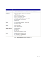
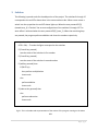
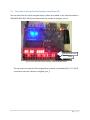
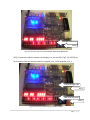
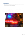
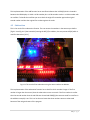
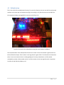
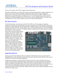
Addition, Subtraction, and Multiplication of
Unsigned Binary Numbers Using FPGA
Author: Justin Hodnett
Instructor: Dr. Janusz Zalewski
CEN 3213 Embedded Systems Programming
Florida Gulf Coast University
Ft. Myers, Fl
Friday, October 02, 2009
1|Page
1 Introduction
A Field-Programmable Gate Array is an integrated circuit designed to be configured by the
customer or designer after manufacturing. Configuration of the FPGA is commonly done using
Hardware Description Language and using the most widely used very-high-speed integrated
circuit hardware description language. The ability for the end user to update functionality after
shipping offers FPGAs many advantages.
FPGAs contain programmable logic components called "logic blocks", and a hierarchy of
reconfigurable interconnects that allow the blocks to be "wired together"—somewhat like a
one-chip programmable breadboard. Logic blocks can be configured to perform complex
combinational functions, or merely simple logic gates like AND and XOR. In most FPGAs, the
logic blocks also include memory elements, which may be simple flip-flops or more complete
blocks of memory.[1]
The DE2 board features a state-of-the-art Cyclone® II 2C35 FPGA in a 672-pin package. All
important components on the board are connected to pins of this chip, allowing the user to
control all aspects of the board’s operation. [2]
1.1 Project Overview
Software provided with the DE2 board features the Quartus® II Web Edition CAD system, and
the Nios® II Embedded Processor. Also included are several examples, tutorials, and
documentation. Traditionally, FPGA boards meant for educational use lack documentation and
examples of what the hardware can do. This is not the case with the Altera DE2 board. Along
with the extensive documentation and examples are several sites dedicated to programming in
VHDL with this board and the Xilinx board. Shown below are a list of features of the board and a
non-extensive list of the board’s capabilities.
2|Page
Fig. 1.1 A list of features for the Altera DE2 [2]
3|Page
Fig. 1.2 A list of some possible projects capable of running on the Altera DE2 [2]
4|Page
1.1 Project Status: October 2, 2009
As of October 2, 2009, I have installed the Quartus II software as described in the Voelmle
article. I sent in my necessary information to receive a License for the Quartus software. I
was also able to go through the example given in the setup of the board and the
hello_world and up_down_counter examples.
1.2 Project Status: October 30, 2009
As of October 30, 2009, I have been able to compile and run most of the requirements
specified in the Problem Description. The requirements need to be revised after an initial
look at the running program. The program only displays the answer while SW[1] is being
held. Also I want to look at instead of a clear key being used, to make that key a subtract
key. The numbers don’t really need to be cleared because when they are saved by the
save_1 and save_2 keys the old values are over-written.
1.3 Project Status: December 4, 2009
As of December 4, 2009 the program has grown the ability to add numbers to all simple
math functions (plus, minus, multiply, and divide). Not all number combinations work
with all functions. This problem has to do with how binary numbers are dealt with and
binary to integer conversion. This problem may also be attributed to the way these
numbers are handled on the Altera DE2 board, but it is unlikely. Division in VHDL is more
difficult than expected. In VHDL the numbers have to be changed to integers, the math
performed, and then changed back to the binary form. So while this was functionality that
I eventually wanted to add, because of the time restriction and level of difficulty I will not
be adding the function.
5|Page
2
Problem Description
-The user shall provide two 16-bit unsigned binary number via 16 toggle switches (SW0 to
SW15) , 1 number at a time.
Rationale: Input is needed to run the program. To allow the user to input binary
numbers the system will store the state of the switches as a binary number. A switch in
the up position represents a 1 in binary and a switch in the down position represents a 0
in binary.
-The system shall display the 16-bit binary numbers as the user enters them on the LEDs above
the corresponding input on the switches.
Rationale: The numbers entered will have a visual component to assist the user entering
them from the switches.
-The system shall capture the positions of the switches and save the positions as a binary
number. The 2 binary numbers entered on the switches when the blue keys on the Altera DE2
board are pressed. The first number will be saved to memory when KEY3 is pressed and the
second number will be save when KEY2 is pressed.
Rationale: The system has to store the numbers to do operations on them. KEY3 will
signify that the user has entered in the first number to be added. The same is true for
KEY2 and the second number entered.
-The system shall perform the necessary math calculations on the 2 binary numbers when KEY1
or KEY0 is pressed and display the result on the red LEDs above the switches.
Rationale: The system needs a signal to start math operations on the numbers and to
display. The output will use the same red LEDs above the switches to output the result.
6|Page
3 Solution
The following is pseudo-code for the add portion of the project. The switches 0 through 15
correspond to the red LEDs above them in the same number order. When a user moves a
switch into the up position the red LED above lights up. When the user presses KEY[3]
(named save_1) it “latches” the current configuration of the switches 0 through 15. The
same effect is achieved when the user presses KEY[2] (save_2). When the remaining keys
are pressed, the program performs addition and clears the numbers repectively.
--pseudo code
LEDR = SW; -- To make the lights correspond to the switches
if (if save1 key pressed)
save the state of the switches in first number
if (if save2 key pressed)
save the state of the switches in second number
if (add key pressed) then
if (SW17 up)
then perform multiplication
show result
else
perform addition
show result
if (subtract key pressed) then
else
perform subtraction
show result
Fig 3.1 This is a Pseudo-code representation of the actions of the program running on the Altera
DE2.
7|Page
The following is code developed to run on the Altera DE2. It is a prototype and does not
represent a final product. Some known defects with this code is that whenever a switch is
up it will display the LED on, except for when the user presses KEY[1] to add the numbers
and display the result. Also the user has to hold KEY[1] in order to display the result. This
code was developed only for the addition function and does not have an overflow signal.
-- unsigned_binary_add.vhd
--- Author: Justin Hodnett ([email protected])
-- CEN 3213 Embedded Systems Programming
-- Florida Gulf Coast University
--- 30-10-2009 created
library ieee;
use ieee.std_logic_1164.all;
use ieee.numeric_std.all;
Use Ieee.std_logic_unsigned.all;
entity unsigned_binary_add is
port (
save_1, save_2, add, clr, clk: in std_logic; SW : in std_logic_vector(15 downto 0);
LEDR : out std_logic_vector(15 downto 0)
);
end unsigned_binary_add;
architecture rtl of unsigned_binary_add is
signal unsigned_num_1: std_logic_vector(15 downto 0);
signal unsigned_num_2: std_logic_vector(15 downto 0);
begin
process(save_1, save_2, add, clr, clk)
begin
LEDR <= SW;
if (save_1=’0’) then
unsigned_num_1 <= SW;
end if;
if (save_2=’0’) then
unsigned_num_2 <= SW;
end if;
if (add=’0’) then
LEDR <= unsigned_num_1 + unsigned_num_2;
end if;
if (clr=’0’) then
unsigned_num_1 <= “0000000000000000”;
unsigned_num_2 <= “0000000000000000”;
end if;
end process;
end rtl;
Fig 3.2 This is a prototype of code developed for the unsigned_binary_math project.
8|Page
3.1 The results of testing this functionality on the Altera DE2.
The user enters the first 16-bit unsigned binary number to be added. In this case the number is
1000 0010 0101 0011. KEY[3] is pressed to save the number to unsigned_num_1.
1000 0010 0101 0011
KEY[3]
Fig 3.1.1 The user sets the first number “1000 0010 0101 0011”
The user enters the second 16-bit unsigned binary number to be added [Fig 3.1.2]. KEY[2]
is pressed to save the number to unsigned_num_2.
9|Page
0001 0010 0100 0101
KEY[2]
Fig 3.1.2 The user sets the second number “0001 0010 0100 0101”
KEY[1] is pressed to add the numbers and display it on the red LEDs [Fig 3.1.3]. KEY[0] can
be pressed to clear the numbers saved in unsigned_num_1 and unsigned_num_2.
1001 0100 1001 1000
KEY[1]
1001 0100 1001 1000
KEY[1]
Fig 3.1.3 The user presses Key[1] to display answer.
10 | P a g e
4 Implementation
The final code developed for this project includes the functionality of addition, subtraction, and
multiplication. The below pictures are the end result.
4.1 Addition
This is the result of the addition function. The user enters the number “0000 0000 1111 1111” for the
first number in the operation [Fig 4.1.1]. The user then enters “0000 0000 0000 0001” for the second
number in the operation [Fig 4.1.2]. When KEY[1] is pressed the user gets the output of the program for
the addition of these two numbers [Fig 4.1.3].
Fig 4.1.1 The user enters the first number
11 | P a g e
Fig 4.1.2 The user enters the second number.
Fig 4.1.3 The result of the addition of the numbers
12 | P a g e
This implementation of the add function has an overflow indicator that is LEDG[8] which is located in
between the HEX displays. In VHDL a 16 bit number plus a 16 bit number results in a 16 bit number with
no overflow. To handle the overflow you must check the original first number against the original
second number and also the original first number against the result.
4.2 Subtraction
This is the result of the subtraction function. The user enters the numbers in the same way as before
[Fig 4.1.1 and Fig 4.1.2] but instead of pressing the KEY[1] for addition, the user presses KEY[0] which is
used for subtraction [4.2.1].
Fig 4.2.1 The result of the subtraction using the same numbers as addition.
This implementation of the subtraction function has a check for which number is larger. If the first
number is larger than the second, then the subtraction occurs as normal. If the first number is smaller
than the second number than the red LEDs are cleared and LEDG[8] (the same one used for overflow in
the addition example) is set. This is to let the user know that these numbers were not subtracted
because of the unsigned nature of the program.
13 | P a g e
4.3 Multiplication
This is the result of the multiplication function. To access this function, the user sets the first and second
numbers in the same way as the above tests [Fig 4.1.1 and Fig 4.1.2], but the user must set SW[17] to
the up position before pressing KEY[1] to view the result [Fig 4.3.1].
Fig 4.3.1 The result of the multiplication using the same numbers as addition.
This implementation of the multiplication function has a check to see if the number is greater than the
16 bits allowed to display. If the number is too large than the green LED is lit so that the user knows that
there is more to the answer that is not being displayed. In binary multiplication a 16 bit number
multiplied by another 16 bit number results in a 32 bit number so the most significant bit is at position
31 while the red LEDs only display to 15.
14 | P a g e
4.4 The code for the end product
-- unsigned_binary_math.vhd
--- Author: Justin Hodnett ([email protected])
-- CEN 3213 Embedded Systems Programming
-- Florida Gulf Coast University
--- 30-10-2009 Created
-- 03-12-2009 Last Edited
-library ieee;
use ieee.std_logic_1164.all;
use ieee.numeric_std.all;
use Ieee.std_logic_unsigned.all;
entity unsigned_binary_math is
port (
save_1, save_2, add, sub, SW17, clk: in std_logic; SW : in std_logic_vector(15 downto 0);
LEDR : out std_logic_vector(15 downto 0); LEDG8: out std_logic
);
end unsigned_binary_math;
architecture rtl of unsigned_binary_math is
signal unsigned_num_1: std_logic_vector(15 downto 0);
signal unsigned_num_2: std_logic_vector(15 downto 0);
signal unsigned_num1: std_logic_vector(31 downto 0);
signal unsigned_num2: std_logic_vector(31 downto 0);
signal unsigned_answer: std_logic_vector(31 downto 0);
begin
process(save_1, save_2, add, sub, SW17, clk)
begin
LEDR <= SW;
LEDG8 <= '0';
15 | P a g e
if (save_1='0') then
unsigned_num_1 <= SW;
end if;
if (save_2='0') then
unsigned_num_2 <= SW;
end if;
if (add='0') then
if (SW17='1') then
unsigned_answer <= unsigned_num_1 * unsigned_num_2;
LEDR <= unsigned_answer(15 downto 0);
if (unsigned_answer(31) = '1') then
LEDG8 <= '1';
end if;
if (unsigned_answer(30) = '1') then
LEDG8 <= '1';
end if;
if (unsigned_answer(29) = '1') then
LEDG8 <= '1';
end if;
if (unsigned_answer(28) = '1') then
LEDG8 <= '1';
end if;
if (unsigned_answer(27) = '1') then
LEDG8 <= '1';
end if;
if (unsigned_answer(26) = '1') then
LEDG8 <= '1';
end if;
if (unsigned_answer(25) = '1') then
LEDG8 <= '1';
end if;
if (unsigned_answer(24) = '1') then
16 | P a g e
LEDG8 <= '1';
end if;
if (unsigned_answer(23) = '1') then
LEDG8 <= '1';
end if;
if (unsigned_answer(22) = '1') then
LEDG8 <= '1';
end if;
if (unsigned_answer(21) = '1') then
LEDG8 <= '1';
end if;
if (unsigned_answer(20) = '1') then
LEDG8 <= '1';
end if;
if (unsigned_answer(19) = '1') then
LEDG8 <= '1';
end if;
if (unsigned_answer(18) = '1') then
LEDG8 <= '1';
end if;
if (unsigned_answer(17) = '1') then
LEDG8 <= '1';
end if;
if (unsigned_answer(16) = '1') then
LEDG8 <= '1';
end if;
else
unsigned_answer (15 downto 0) <=unsigned_num_1 + unsigned_num_2;
if (unsigned_num_1(15) = unsigned_num_2(15)) and
(unsigned_num_1(15)/=unsigned_answer(15)) then
LEDG8 <= '1';
LEDR <= unsigned_answer (15 downto 0);
17 | P a g e
else
LEDR <= unsigned_answer (15 downto 0);
end if;
end if;
end if;
if (sub='0') then
unsigned_answer <= unsigned_number_1 – unsigned_number_2;
if (unsigned_num_1 > unsigned_number_2) then
LEDR <= unsigned_answer (15 downto 0);
else
LEDG8 <= '1';
end if;
end if;
end process;
end rtl;
Fig 4.1 The source code for the final product.
Compiling this program follows the same method as described in the Voelmle article. When assigning
pins, it is easiest to load the pin assignment file and change the corresponding pins.
Key[3] changed to save_1
Key[2] changed to save_2
Key[1] changed to add
Key[0] changed to sub
SW[17] changed to SW17
LEDG[8] changed to LEDG8
The clk assignment is the same as in the Voelmle article.
18 | P a g e
5 Conclusion
This project started as a simple addition of two 16 bit binary numbers and ended as an almost
complete simple calculator. The division function was dropped due to its complexity. The
addition functionality was the first to be developed and the subtraction and multiplication were
developed after that. The program can perform simple mathematical calculations such as
addition, subtraction, and multiplication. The program is in a state to be released and will
perform as tested as long as the user compiles the program correctly.
This project has given me several experiences. The biggest positive experience was that I
learned more about VHDL. I specifically chose this project because I felt that I was weaker in
VHDL programming than I should be. Now I have a little better understanding of it. Another
positive experience from this project was that the I was able to see a visual representation of
what my VHDL programming was doing. Viewing time graphs did help to an extent in my
previous experiences with VHDL, but I liked having a visual aspect to show what was happening.
The most negative experience was that I did not have enough time to develop the division
functionality. I would have liked a more complete simple binary calculator, but with other
projects competing for my time and attention the full development had to wait. Another
negative experience was learning more VHDL.
The impact of this technology is limited. The project is nice for students learning binary math,
but I don’t foresee many applications outside of education. It gives users a chance to enter
binary numbers and modify them using the functions and displays the answers in an easy to use
and easy to read method.
I would like to return to this project at some point in the future. I would like to add more
functions and maybe change the input and output methods. I am interested in VHDL but I feel
very limited by my time to devote to learning it and the lack of instruction for programming in
VHDL. I did not feel that the resources that I found online really gave me an understanding of
why something should be done a certain way. This was the case with division which required a
conversion to an integer, then the division, and then conversion back to the binary number.
19 | P a g e
6 References
[1] Wikipedia, Field-Programmable Gate Array, 1 October 2009, http://en.wikipedia.org/wiki/FPGA
[2] DE2 Development and Education Board User Manual, Version 1.4, Altera Corp.
San Jose, CA, 2006, ftp://ftp.altera.com/up/pub/Webdocs/DE2_UserManual.pdf
[3] M. Schoeberl, The FPGA Hello World Example, August 4, 2006,
www.jopdesign.com/cyclone/hello_world.pdf
[4] J. Voelmle, Investigation of Altera DE2 Development and Education Board , 1/20/09,
http://itech.fgcu.edu/faculty/zalewski/CEN3213/files/Voelmle_FPGA_Study.pdf
[5] John Loomis, Altera DE2 Project Diglab1, 9/1/2008,
http://www.johnloomis.org/digitallab/diglab/diglab1/diglab1.html
20 | P a g e