1
CHIP CHARACTERIZATION:
MAN-HOUR REDUCTION AND INCREASED FUNCTIONALITY
TESTING WITH AUTOMATION IMPROVEMENTS
THESIS
Presented to the Graduate Council of
Texas State University-San Marcos
in Partial Fulfillment
of the Requirements
for the Degree
Master of SCIENCE
by
Robert C. Murphy, PhD, M.S., B.S.
San Marcos, Texas
May 2007
CHIP CHARACTERIZATION:
MAN-HOUR REDUCTION AND INCREASED FUNCTIONALITY
TESTING WITH AUTOMATION IMPROVEMENTS
Committee Members Approved:
_______________________________
Deborah East
_______________________________
Jawad Drissi
_______________________________
Granville Ott
Approved:
________________________
J. Michael Willoughby
Dean of the Graduate College
ACKNOWLEDGEMENTS
I am very thankful to Dr. East, Dr. Otto, and Dr. Drissi for their guidance
and support. I would also like to thank the company C.L. for presenting and
allowing me to work on this problem. It has been a very intense and rewarding
experience. I would also like to thanks the engineers for their invaluable
assistants.
This manuscript was submitted on March 6, 2007.
iii
TABLE OF CONTENTS
ACKNOWLEDGEMENTS.....................................................................................iii
ABSTRACT .........................................................................................................xii
CHAPTER 1 ......................................................................................................... 1
BACKGROUND.................................................................................................... 1
INTRODUCTION .................................................................................................. 1
1.1. Project Motivation .......................................................................................... 1
1.2. Project Description................................................................................ 4
1.3. Software Platform Used to Implement System...................................... 7
1.4. Summary of Interview / Knowledge Acquisition .................................... 7
1.5. Additional Existing Documents, Synonyms, etc. ................................. 10
1.6 Organization of Thesis ......................................................................... 10
1.7. Background......................................................................................... 11
1.7.1 Resolution..................................................................................... 13
1.7.2 Range ........................................................................................... 15
1.7.3 Amplification ................................................................................. 16
1.7.4 Code Width ................................................................................... 17
1.7.5 Conversion Errors......................................................................... 20
CHAPTER 2 ....................................................................................................... 29
PERFORMANCE METRICS FOR ADC ............................................................. 29
INTRODUCTION ................................................................................................ 29
2.1 Static Performance .............................................................................. 30
iv
2.1.1 Histogram Analysis ....................................................................... 30
2.1.2 Gaussian ...................................................................................... 31
2.1.3 DNL Affect on Histogram .............................................................. 35
2.1.4 Averaging ..................................................................................... 36
2.1.5 Flicker Free Bits............................................................................ 37
2.4 Dynamic Performance.......................................................................... 39
2.4.1 Windowing .................................................................................... 40
2.4.2 Signal Analysis Statistics .............................................................. 46
CHAPTER 3 ....................................................................................................... 48
ANALYSIS APPLICATION ................................................................................. 48
CHAPTER 4 ....................................................................................................... 57
UML.................................................................................................................... 57
INTRODUCTION ................................................................................................ 57
4.1 General Description for ADC Family .................................................... 58
4.1.1 UML Class Model ......................................................................... 64
4.1.2 UML State Model .......................................................................... 65
4.2 Microcontroller ..................................................................................... 84
4.3 Bench Test Environment...................................................................... 91
4.3.1 Class Model .................................................................................. 92
4.3.2 State Model................................................................................... 93
4.3.3 Interaction Model .......................................................................... 95
4.4 Automation Test Environment............................................................ 106
4.4.1 Class Model ................................................................................ 107
4.4.2 State Model................................................................................. 109
v
4.4.3 Interaction Model ........................................................................ 115
CHAPTER 5 ..................................................................................................... 116
IMPLEMENTATION.......................................................................................... 116
INTRODUCTION .............................................................................................. 116
5.1 PROTOCOLS .................................................................................... 117
5.1.1 SPI.............................................................................................. 117
5.1.2 GPIB ........................................................................................... 118
5.1.3 RS485......................................................................................... 119
5.1.4 Peripherals Interfacing................................................................ 119
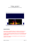
5.2 User Interface .................................................................................... 134
CHAPTER 6 ..................................................................................................... 163
CONCLUSION.................................................................................................. 163
BIBLIOGRAPHY............................................................................................... 164
vi
LIST OF TABLES
TABLE 1 CALCULATED LSB VALUES FOR DIFFERENT RESOLUTIONS...... 19
TABLE 2 IDEAL RESOLUTION.......................................................................... 19
TABLE 3 IDEAL SIGNAL-TO-NOISE ................................................................. 20
TABLE 4 WINDOWS METRICS ......................................................................... 45
vii
LIST OF FIGURES
FIGURE 1 OVERALL PROJECT LAYOUT .......................................................... 4
FIGURE 2 INPUT SIGNAL SINE WAVE 100 HZ................................................ 14
FIGURE 3 ADC 3 BIT CONVERSION OF SINE WAVE ..................................... 14
FIGURE 4 ADC 16 BITS CONVERSION OF 100 HZ SINE WAVE .................... 15
FIGURE 5 RANGE (0-10)V AND (-10 TO +10)V................................................ 16
FIGURE 6 ADC 3-BITS CODE WIDTH AND TRANSITIONS............................. 18
FIGURE 7 DIFFERENTIAL NONLINEARITY ..................................................... 22
FIGURE 8 INTEGRAL NONLINEARITY............................................................. 23
FIGURE 9 OFFSET ERROR .............................................................................. 24
FIGURE 10 GAIN ERRORS ............................................................................... 25
FIGURE 11 ALIAS TIME DOMAIN SIGNAL ....................................................... 26
FIGURE 12 ALIASING IN THE FREQUENCY DOMAIN .................................... 28
FIGURE 13 NON-IDEAL ADC HISTOGRAM ..................................................... 31
FIGURE 14 GAUSSIAN NOISE AND PDF......................................................... 32
FIGURE 15 HIGH DNL AFFECT ON HISTOGRAM ........................................... 35
FIGURE 16 PERIODIC AND NON-PERIODIC ANALOG SIGNALS ................. 40
FIGURE 17 FFT PERIODIC AND NON-PERIODIC SIGNAL ............................ 41
FIGURE 18 SINE WAVE WINDOWED WITH HAMMING .................................. 42
FIGURE 19 MAINLOBE AND SIDELOBE OF WINDOWS ................................. 43
FIGURE 20 FREQUENCIES BLEARING FROM WINDOWING......................... 44
FIGURE 21 WINDOWS SINE WAVE PLOT...................................................... 46
FIGURE 22 BASIC DYNAMIC PERFORMANCES............................................. 49
FIGURE 23 POWER SPECTRUM OF SIGNAL ................................................. 50
FIGURE 24 SNR FLOW CHART....................................................................... 51
FIGURE 25 SDR DIAGRAM............................................................................... 52
FIGURE 26 SDR FLOWCHART......................................................................... 53
FIGURE 27 SIGNAL TO PEAK NOISE MAPPING............................................. 54
FIGURE 28 SPN PSEUDO-CODE ..................................................................... 55
FIGURE 29 PSEUDO-CODE FOR SINAD ......................................................... 56
FIGURE 30 CS5530 ADC INTERNAL................................................................ 59
FIGURE 31 FRONT END CONFIGURATION .................................................... 59
FIGURE 32 CS5530 REGISTERS ..................................................................... 60
FIGURE 33 CS5531/32/33/34 ADC INTERNAL ................................................. 61
FIGURE 34 CS5531-34 FRONT END ................................................................ 62
viii
FIGURE 35 CS5531/32/33/34 REGISTER DIAGRAM ....................................... 63
FIGURE 36 CLASS DIAGRAM OF DUT ............................................................ 65
FIGURE 37 SYSTEM INITIALIZATION .............................................................. 67
FIGURE 38 ADC RESET STATE MODEL ......................................................... 68
FIGURE 39 READ, WRITE, AND DATA CONVERSION TIMING DIAGRAMS .. 69
FIGURE 40 WRITE CYCLE................................................................................ 70
FIGURE 41 READ CYCLE STATE MODEL ....................................................... 71
FIGURE 42 SINGLE DATA CONVERSION ....................................................... 72
FIGURE 43 LOAD COMMAND SUB-STATE OF DATA CONVERSION............ 73
FIGURE 44 CONFIGURATION REGISTER PIN OUT ....................................... 74
FIGURE 45 READ REGISTER STATE MODEL................................................. 75
FIGURE 46 WRITE REGISTER STATE MODEL ............................................... 76
FIGURE 47 SELF CALIBRATION STATE MODEL CS5531-5534 ..................... 78
FIGURE 48 SYSTEM CALIBRATION STATE MODEL FOR CS553X ............... 79
FIGURE 49 CONVERSION REGISTER DATA OUTPUT DESCRIPTIONS....... 80
FIGURE 50 CS5530 CONVERSION DATA OUTPUT DESCRIPTIONS ............ 81
FIGURE 51 SINGLE DATA CONVERSION STATE MODEL ............................. 82
FIGURE 52 CONTINUOUS CONVERSION STATE MODEL............................. 83
FIGURE 53 BOARD LAYOUT ........................................................................... 84
FIGURE 54 C8051F320 MICROCONTROLLER INTERNAL LAYOUT .............. 87
FIGURE 55 C8051F320 BLOCK DIAGRAM....................................................... 88
FIGURE 56 USBXPRESS DATA FLOW ............................................................ 89
FIGURE 57 EXPRESS API FOR PC AND DUT (DEVICE UNDER TEST) ........ 90
FIGURE 58 MICROCONTROLLER STATE MODEL ......................................... 91
FIGURE 59 BENCH TEST CLASS MODEL ....................................................... 92
FIGURE 60 BENCH TEST STATE MODEL ....................................................... 94
FIGURE 61 USE CASE DIAGRAM FOR POWER SUPPLY ............................ 102
FIGURE 62 SILICON THERMAL USE CASE DIAGRAM ................................. 103
FIGURE 63 DUT USE CASE DIAGRAM .......................................................... 104
FIGURE 64 EVALUATION SOFTWARE SEQUENCE “EVAL553X_U.EXE” ... 105
FIGURE 65 AUTOMATION LAYOUT............................................................... 107
FIGURE 66 AUTOMATION CLASS MODEL.................................................... 108
FIGURE 67 AUTOMATION POWER INITIALIZATION STATE MODEL .......... 110
FIGURE 68 SETTING POWER SUPPLY VOLTAGES AND CURRENT
VALUES .................................................................................................... 112
FIGURE 69 SILICON THERMAL TEMPERATURE VALUES........................... 114
ix
FIGURE 70 TEST ENGINEERS AND TESTERS RELATIONSHIP TO
AUTOMATIC TEST ENVIRONMENT........................................................ 115
FIGURE 71 DATA SOURCE SELECTION....................................................... 137
FIGURE 72 SUCCESSFUL COMMUNICATION .............................................. 138
FIGURE 73 VERSION IDENTIFICATIONS ...................................................... 139
FIGURE 74 MENU DRIVEN ............................................................................. 140
FIGURE 75 SETUP PANEL ............................................................................. 141
FIGURE 76 SINGLE CONVERSION MODE USING SOFTWARE TIMER ..... 143
FIGURE 77 CALIBRATION .............................................................................. 144
FIGURE 78 CHANNEL SETUP PANEL ........................................................... 145
FIGURE 79 DATA COLLECTION WINDOW (ANALYSIS) ............................... 146
FIGURE 80 CONFIGURATION PANEL (# SAMPLES, AVERAGE, FFT
WINDOW, HISTOGRAM WIDTHS)........................................................... 147
FIGURE 81 CONFIGURATION SAMPLE NUMBER DROP DOWN LIST........ 148
FIGURE 82 TIME DOMAIN 1024 SAMPLES ................................................... 149
FIGURE 83 FFT OF CONVERTED DATA ....................................................... 150
FIGURE 84 ZOOM SEGMENT OF THE PLOT ................................................ 151
FIGURE 85 ERROR MESSAGE WHEN CURSORS ARE OUT OF ORDER ... 152
FIGURE 86 HISTOGRAM OF ZERO VOLT INPUT ......................................... 153
FIGURE 87 AVERAGE PLOTTED 2 ................................................................ 154
FIGURE 88 AVERAGE PLOTTED 10 .............................................................. 155
FIGURE 89 NO CALIBRATION........................................................................ 156
FIGURE 90 WITH OFFSET AND GAIN CALIBRATIONS ............................... 157
FIGURE 91 AUTOMATION PANEL ................................................................. 158
FIGURE 92 CS5530 SETUP PANEL .............................................................. 161
FIGURE 93 CS5530 DATA COLLECT PANEL ................................................ 162
x
LIST OF EQUATIONS
EQUATION 1 CODE WIDTH.............................................................................. 17
EQUATION 2 IDEAL CODE WIDTH CALCULATION ........................................ 19
EQUATION 3 SIGNAL TO NOISE RATIO.......................................................... 20
EQUATION 4 ANALOG TO DISCRETE SIGNAL REPRESENTATION ............. 26
EQUATION 5 ALIAS FREQUENCY GENERATED ............................................ 27
EQUATION 6 GAUSSIAN PROBABILITY DENSITY ......................................... 32
EQUATION 7 MEAN .......................................................................................... 32
EQUATION 8 STANDARD DEVIATION OF DIGITIZED SIGNAL ...................... 32
EQUATION 9 SNR CALCULATION WITH NOISES........................................... 37
EQUATION 10 WINDOWING FREQUENCY RESOLUTION ............................. 44
EQUATION 11 SIGNAL-TO-NOISE RATIO ....................................................... 48
EQUATION 12 SIGNAL-TO-NOISE PLUS DISTORTION.................................. 48
EQUATION 13 SIGNAL-TO-DISTORTION RATIO ............................................ 48
EQUATION 14 SIGNAL-TO-PEAK NOISE......................................................... 48
xi
ABSTRACT
CHIP CHARACTERIZATION:
MAN-HOUR REDUCTION AND INCREASED FUNCTIONALITY TESTING
WITH AUTOMATION IMPROVEMENTS
by
Robert C. Murphy
Texas State University-San Marcos
May 2007
SUPERVISING PROFESSOR: DEBORAH EAST
Chip design expansion increases linearly with new products, thus device
characterization tests have increased exponentially and created a chip design
bottleneck. If there is only one function (herein designated as “A”), “A” need only
test function “A.” If there are two functions, “A” and “B”, then test sets will be “A,”
“B,” “AB,” and “BA.” If there are three functions, ”A,” “B,” and “C,” then test sets
“A,” “B,” “C,” “AB,” “AC”, “BA,” “BC,” “CA,” “CB,” “ABC,” and so forth.
xii
The objective of this thesis is to automate manual test procedures so that
design bottlenecks can be eliminated and device characterization can be
improved. In achieving the stated objective, it will be necessary to develop a
framework that attains and integrates commonality, maintainability, and
reusability.
xiii
CHAPTER 1
BACKGROUND
INTRODUCTION
1.1. Project Motivation
C.L. Corporation (C.L.) is a major producer of industrial chips used in oil
exploration, residential power consumption and weigh scale application. C.L. is
also a leading producer analog to digital converters, (ADC). Chip design
expansion increases linearly with new products, thus device characterization
tests have increased exponentially and created a chip design bottleneck. If
there is only one function (herein designated as “A”), “A” need only test function
“A.” If there are two functions, “A” and “B”, then test sets will be “A,” “B,” “AB,”
and “BA.” If there are three functions, ”A,” “B,” and “C,” then test sets “A,” “B,”
“C,” “AB,” “AC”, “BA,” “BC,” “CA,” “CB,” “ABC,” and so forth.
C.L. characterization engineers find it challenging to keep up with the
demands placed upon them. Chip validation procedures focus on everything
1
2
from highly integrated analog and digital tests to system level power
management and custom “system on” chip tests.
The objective of this project is to automate C.L.’s manual test procedure
so that design bottlenecks can be eliminated and device characterization can be
improved. In achieving the stated objective, it will be necessary to develop a
framework that attains and integrates commonality, maintainability, and
reusability.
Currently, C.L. device characterization is a highly manual process that
involves extensive operator intervention and control. The engineer manually sets
up the power supplies, device temperature, writes to the DUT (device under test),
then records multi-meter measurements by hand. This process is tedious, time
consuming, and lends itself to errors. In essence, a typical validation procedure
requires the use of at least four different instruments which results in the
necessity of four different protocols to control the instruments.
Each instrument has its own exclusive control language. Power meter,
ADC microchip validation/characterization, and testing procedures utilize RS232, RS-485, GPIB (IEEE-488), and USB 2.0 protocols. Power supplies and
digital multi-meters use GPIB. Silicon Thermal DUT temperature set uses RS232 and a network version of RS-232 called RS-485. The (customized) board
which holds the DUT uses USB 2.0 to communicate with the microcontroller, and
3
the microcontroller then communicates with the chips on the evaluation board.
The microcontroller uses protocols I2C or SPI for chip communication.
In this project, I shall integrate source and measurement equipment with
the customized board to test microchips. In personal interviews with C.L.’s
engineers, four crucial criteria emerged as follow:
•
Ease of use
•
Modularity
•
Interchangeability
•
Flexibility
The key project goal is to improve C.L.’s test methodologies by automating
testing techniques. The test project should use easy, flexible, modular,
interchangeable components. Whenever feasible, the interface screen should
match as closely as possible to the actual test measurement instruments.
The programming language used to set up the aforementioned
methodologies shall be Labwindows.
4
1.2. Project Description
FIGURE 1 OVERALL PROJECT LAYOUT
Once again, the objective of this project is automating the chip validation
procedure and developing a technique for testing specific functions of a chip. To
5
achieve this task I grouped the project into three phases. Phase 1 is developing
an application to communicate with the test chips, phase 2 is developing drivers
to communicate with the test instrument, and phase 3 is integrating phase 1 and
phase 2 together resulting in the automatic tester. Figure 1.1 shows the layout
of this project.
This application overcomes the human error and speed up the validation
procedure. It is design based on the concept of virtual instrument. Virtual
instruments describe the combination of programmable instruments with generalpurpose PCs. Virtual instruments contain a GUI for controlling its functions by
the PC. A test engineer can easily set the peripherals for several values that are
automatically changed by the host computer during a run. The output consists of
test output parameters, peripherals values, and chip register values.
Product Features and Benefits:
• Automatic so reduction in human error
•
Reduction in man hours for validation
•
Accuracy in test setup and reading
•
Easy to use
•
GUI for each peripheral
•
User Friendly
•
Product Constraint:
•
Graphical User Interface
6
•
Automatic setting of peripherals
•
Automatic setting of Chip register values
•
All register values and peripherals setting store in a file
•
Stand alone operation
•
Monitors: 800x600 minimum resolutions at 256 colors
•
Computer with GPIB card, RS232 port, and USB port
•
I/O: One or two button mouse and standard 101-key board
•
Mhz: PIII 1.0 Ghz
•
Power Supply with GPIB or RS232 port (HP3458)
•
Keithley Digital Multimeter 197A GPIB port
•
Silicon Thermal Temperature controller with RS232 port
•
Power Setting up to 10 values
Hardware Constraint:
• Monitors: 800x600 minimum resolutions at 256 colors
•
Computer with GPIB card, RS232 port, and USB port
•
I/O: One or two button mouse and standard 101-key board
•
Mhz: PIII 1.0 Ghz
•
Power Supply with GPIB or RS232 port (HP3461A)
•
Keithley Digital Multimeter 197A GPIB port
•
Silicon Thermal Temperature controller with RS485 port
Assumptions:
7
•
Above instrument are available
•
Tester and/or Test Engineer knows how to connect GPIB devices
•
Tester and/or Test Engineer comfortable with windows and mouse
•
Tester and/or Engineer knows excel spreadsheet and how to import
•
USB 2.0 communication is bug free
1.3. Software Platform Used to Implement System
I used LabWindows/CVI to develop this application. LabWindows/CVI is a
test and measurement ANSI C development environment. It includes a 32-bit
compiler and linker with advanced editing and debugging tools.[1][2] It is open
which means one can incorporate other compilers and produce DLLs for other
environments. LabWindows/CVI includes a comprehensive suite of libraries
targeted at instrumentation applications, from instrument control to data analysis
and graphing. It also includes CodeBuilder and interactive function panels. [3]
1.4. Summary of Interview / Knowledge Acquisition
Robert: Hi M S how are you doing today?
M S: I am doing great.
Robert: How is the new born and has your daughter accepted him yet?
MS: New born is fine and no, the daughter has not accepted him.
Robert: Well, how is work going in the industrial group?
8
MS: Well, it would be a lot better if we had the test procedure automated. I have
several new chips coming in that need to be validated.
Robert: What is it that you need to automate and how can I help?
M S: As you know we have a test board and have a chip that we place on the
board. The board is connected to the host computer through the USB port. We
would like an application to communicate with the chip and write to different
registers on the chip.
Robert: What type of protocol are you using to communicate with the device
under test?
M S: I think that it is SPI to write to the register and to read information from the
registers.
Robert: So what are some of the test features that you want to do on the chip?
M S: Well, I would like Normal test of the chip and several signal analysis tests
on the chip.
Robert: What type of signal analysis test on the chip that you would like?
M S: Signal FFT and Noise FFT.
Robert: What else would you like in your output?
M S: Well, I would like to see plots Fast Fourier Transforms and magnitude and
phase of the signal.
Robert: What else would you like?
M S: I would like for it to be totally automated.
Robert: Please elaborate.
M S: On the test board there are plug-ins for power connection. I would like to
adjust the different power supply setting automatically. Also, there are jumpers
that come off the board. Do you know what jumpers are?
Robert: Yes, I understand.
M S: These jumper output voltage values on the board that tell what the output
of the chip is. I would like to store those values in to a file somehow with the chip
configuration.
Robert: That wouldn’t be a problem. What format would you like the output to
be?
9
M S: I would like to be able to open the output file into an excel spreadsheet.
The tester should able to do analysis on the output file values.
Robert: How many power supplies will be used to connect to the testing board
to power up the chip?
M S: There will be only one power supply powering the board and the test chip.
There also will be two digital multimeters to read the value of the header or
jumpers. And there is a thermal controller that needs to be adjusted. It sets the
temperature value of the device.
Robert: What is the interface protocol for these devices?
M S: The protocol is RS 232 and GPIB and the board is connected to the host
computer through the USB bus.
Robert: If you are using the GPIB, there needs to be a PCI-GPIB card or usbGPIB device connected to the computer to communicate to GPIB devices. Do
you have a card?
M S: Well, we probably have one floating around, if not we will order what ever
you need to interface to the instrument.
Robert: What programming language do you want to use?
M S: Well, I would like it to be written in Labwindows and/or Labview.
M S: Do you know Labview or Labwindows?
Robert: Well, I am a Labview expert but I don’t know Labwindows at the
moment. It should not take me long to figure it out though.
M S: Great.
Robert: Do you mind if I record our interview for my thesis?
M S: No problem at all feel free to use it and my name.
Robert: I won’t use your name or the company name directly. I will just use an
alias for the company and your name.
M S: That is okay.
Robert: Is there anything else you would like to add at this moment.
M S: No, I think that I have covered everything so far.
Robert: Well, thanks for the interview and I will start right away on designing the
prototype of the interface and other stuff so that you and your engineer can
overview it.
10
M S: Thanks.
Robert: No thank you. This should be a fun project and feel free to contact via
email or through the phone if you have any last minute suggestions.
1.5. Additional Existing Documents, Synonyms, etc.
GPIB- General Purpose Interface Bus, IEEE-488 protocol
R232- serial communication protocol TX, R, G 3 wires
DAQ- Data Acquisition
ADC – Analog to Digital Converter
DAC – Digital to Analog Converter
I2C - chip protocol pronounce eye square c
SPI - Serial Port Interface
RS484 – serial communication protocol with addressing capability
DUT – Device Under Test
1.6 Organization of Thesis
Chapter 1 covers the software requirements and the methodology used to
attain them. Also, I discuss hardware limitations and constraints and review
background information on analog-to-digital parameters.
In Chapter 2 performance metrics of ADC is discussed. Both static and
dynamic performances are reviewed in details.
In Chapter 3 a review of the analysis application is discuss. I explain how
to calculate and define the signal-to-noise ration, signal-to-distortion ratio, signalto-noise plus distortion, and signal-to-peak noise.
11
In Chapter 4 a general description of analog-to-digital family of chips are
presented. I design a solution to the problem using Unified Model Language
Methodology. I discuss the microcontroller code and the different testing
environment.
Chapter 5 is the implementation phase of the solution. I describe the
development environment for both application and microcontroller code. I
describe event driven programming and the data structures used in the solution.
Graphical User Interfaces of the application are displayed. Both instructions on
how to use the application and description of objects on the panel are given.
1.7. Background
In the following section, I explain the basic of signal acquisition, how
analog to digital converter operate, and some fundamental concepts of ADC.
Signal acquisition is the process of converting a physical phenomenon into data
that a computer can use. [4] A transducer is used to convert a measurement of a
physical phenomenon into an electrical signal. [5] Physical phenomena can be
temperature, force, sound and light. Some examples of transducers are
thermocouples used to measure temperature, photoconductive cells to measure
light, microphones to measure sound, and load cells to measure force and
12
pressure. [6] The electrical signal from the transducer can be of two types digital
or analog.
Most physical phenomena are analog. The information provided in an
analog signal is its level, shape, and frequency. Measuring the level of analog
signal is measuring its voltage level. Measuring the shape of a signal can
provide information about the peak values, slope or integration. To extract
frequency information from an analog signal requires that the signal be Fourier
Transform into the frequency domain from the time domain. [7]
A digital signal has only two possible states ON and OFF. Digital signal is
TTL (Transistor to Transistor Logic). There are only two aspects of a digital
signal measured state and rate. An example of digital signal is the encoded
signal of a motor spinning.
Doing complex analysis with a computer on a signal requires that the
signal be digitized. Digitization is accomplished through an ADC. The ADC
converts an analog signal into 0s and 1s into a word which is an approximate
representation of the magnitude of the input signal. An ADC continuously maps
the analog signal into discrete steps that are represented by digital codes. Each
discrete step represents a fixed value of the voltage reference used. Some
common characteristics of ADC are resolution, range, amplification, and code
width.
13
1.7.1 Resolution
Resolution is the number of bits used to represent an analog signal. [8]
One can look at resolution like the markings on a ruler. The more marks on a
ruler, the more precise the measurements are. The higher the resolution (the
more bits) an ADC has, the greater the number of divisions used to represent a
range. Thus, the smaller a detectable change can be converted. A 3 bit ADC
divides the range into 23 or eight divisions. The binary code goes from 000 to
111 to represent each division. The ADC converts each measurement of the
analog signal to one of the eight divisions. The figure below shows the difference
between a 3 bit ADC and 16 bit ADC used to convert a 100 Hz sine wave
sampled at 1 KHz with 1000 samples taken. A 16 bit ADC has 216 (65536)
divisions. 16 bit ADC is much more accurate representation of the sine wave.
14
FIGURE 2 INPUT SIGNAL SINE WAVE 100 HZ
FIGURE 3 ADC 3 BIT CONVERSION OF SINE WAVE
15
FIGURE 4 ADC 16 BITS CONVERSION OF 100 HZ SINE WAVE
1.7.2 Range
Range is the minimum and maximum analog signal that an ADC can
quantize. Typical, ranges are 0V to 10V (unipolar) or -10V to 10V (bipolar). For
better accuracy the range of the ADC should have the same polarity as the
signal. For example, if the input signals to an ADC is a unipolar value between 0
and 10 volts and the range of the 3 bits ADC is set to 0 to 10 volts. All eight
binary codes are then used to digitize the signal. Each division is a multiple of
1.25 volts. If the ADC is set to bipolar mode from -10 to 10 volts, there are only
four divisions used to digitize the positive signal. Each division is now a multiple
of 2.5 volts. [9]
16
FIGURE 5 RANGE (0-10)V AND (-10 TO +10)V
1.7.3 Amplification
Amplification is the act of amplifying the signal. For the best result the
signal is amplified before digitization. By amplifying the signal it effectively
decreases the input range of an ADC. This allows the ADC to use the maximum
number of digital divisions. For example, if the signal from the transducer is
between 0 and 5 V. It is connected to a 3-bit ADC with a range of 0 to 10V.
With a gain = 1 or no amplification, there are four divisions used to quantize the
signal out of a possible eight divisions. Change the gain to 2, and the input
voltage is now scaled between 0 and 10V. All eight codes can be used to digitize
the signal. In summary, the range, resolution, and amplification determine the
smallest detectable change that an ADC can quantize.
17
1.7.4 Code Width
Code width is the smallest change that a system can detect in a signal.
The code width is calculated with the following equation:
codewidth =
voltageranges
amplification × 2 bits
EQUATION 1 CODE WIDTH
Signal representation is directly correlated to code width. The smaller the code
width is the more accurate the signal representation. From Equation 1.1 the
following axiom can be proven:
•
Larger resolution = smaller code width that results in a more
accurate representation of the signal
•
Larger amplification = smaller code width that results in a
more accurate representation of the signal
•
Larger range = larger code width resulting in less accurate
representation of the signal.
18
FIGURE 6 ADC 3-BITS CODE WIDTH AND TRANSITIONS
If in Figure 1.6 there is a 12 bit ADC, the voltage range is between -5 to
+5 V and gain = 1. [6] The ideal code width is 2.441 mV. Any signal between 0
and 2.441mv will be encoded as 000. Any signal greater then 2.441 mV but less
than 4.882 mV will be encoded as 001 and so on.
The plot also shows that
there are 2N codes and 2N -1 transition. The transitions are represented by the
linear line between the steps. The center of one of the codes is defined as zero,
which means that a bipolar conversion will have one fewer code on half of the
transfer function than the other. This also means that at full-scale, the output
code is described at least 1 LSB (Least Significant Digit) less than the voltage
reference because of the zero code. In Table 1 the actual code width is
19
calculated for different bit size ADC for a full-scale value = ± 3V. 1 count or LSB
can be looked at as the code width.
6Volts
2 Codes
N
EQUATION 2 IDEAL CODE WIDTH CALCULATION
Table 1 CALCULATED LSB VALUES FOR DIFFERENT RESOLUTIONS
Analog-to-Digital Quantization of Full Scale ± 3V
N
12
16
20
24
1 LSB
1.46mV
91.5µV
5.7µV
0.36µV
Table 2 shows the number of codes calculated from 2N and the resolution is the
code width equation with the range being 1.
Table 2 IDEAL RESOLUTION
Ideal ADC Measurement and Resolution
N Bits
# of Codes
Resolution
12
4096
244 ppm
16
65536
15 ppm
20
1,048,576
0.95 ppm
24
16,777,216
0.06 ppm
20
1.7.5 Conversion Errors
An ADC is a quantizing device. There is always quantization error even
in an ideal ADC. When a signal has been digitized, the digital codes
representing the signal can actual differ by as much ± ½ LSB (code width).
Figure 6 shows the quantization error being plotted per code width. The best
that an ideal ADC can do in representing the signal verses quantization noise is
calculated by the following equation. N is the number of ADC bits. [11]
SNR = 6.02 N + 1.76 dB
EQUATION 3 SIGNAL TO NOISE RATIO
The signal to noise ratio (SNR) defines the full scale root mean square of the
sine wave to the root mean square of the quantization noise. [11]
Table 3 IDEAL SIGNAL-TO-NOISE
Ideal Signal to Noise Ratio
N Bits
S/N(dB)
12
74
16
98
20
122
24
146
21
Table 3 shows the best possible signal that an analog-to-digital converter can
produce with the given bits of ADC.
The step-size of a real world ADC can be greater or smaller then the ideal
quantization step size. The changes in step size introduce an additional error
called the differential nonlinearity (DNL). [12] DNL is the difference between the
actual sizes of the code versus the ideal. SNR decreases with an increase in the
DNL. The variation in code size is a function of the matching accuracy of the
elements that compose the converter. Large mismatches in the ADC electrical
converting elements can cause short or wide codes or even cause code to be
missing. These variations can be caused by random environmental changes or
parasitic noises in the system itself. Figure 7 is a plot of the differential
nonlinearity.
22
FIGURE 7 DIFFERENTIAL NONLINEARITY
Integral Nonlinearity (INL) is a measure of the linearity of the entire
transfer function of the ADC. A straight line is drawn between the codes at each
end of the transfer function. Integral nonlinearity is the furthest distance from the
center point of the line and the code. [13] Another method of calculating INL is to
put a full-scale low distortion sine wave into the converter and do an FFT (Fast
Fourier Transform) to calculate the spectral density characteristics converter. [14]
23
Signal/noise and Signal/(noise plus distortion) can be calculated. Figure 5 shows
the integral nonlinearity of the converter.
FIGURE 8 INTEGRAL NONLINEARITY
Offset error is the shift of the zero point in the code. This is the code generated
when the voltage input into the ADC is zero. It is determined from the mean of
histogram of codes. This calculation will be discussed later in this chapter.
Figure 9 is an example of offset. [15]
24
FIGURE 9 OFFSET ERROR
The gain error is the change in the slope of the converter transfer function.
It is the difference between a given code and a line being drawn from the origin
through the 0 volt code value. Figure 7 shows the gain error calculation. [11]
25
FIGURE 10 GAIN ERRORS
Another cause of conversion error is aliasing. Aliasing results when the
sample rate is below the Nyquist Theorem for an incoming signal. A signal x(t)
in the time domain is sampled every ∆t seconds. This time interval is called the
sampling interval or sample period. The reciprocal 1/∆t is the sampling
frequency. It is in unit samples/second. Each discrete value (binary code) of
signal x(t) at time t = 0, ∆t, 2∆t, 3∆t, etc., is a sample. [16] The signal x(t) is now
represented by discrete signals. This is the definition of a digital representation
of a signal.
26
x(t ) = x(0), x( Δt ), x( 2 Δt ), x(3Δt ),..., x( kΔt )
EQUATION 4 ANALOG TO DISCRETE SIGNAL REPRESENTATION
The sample rate is the speed at which a measurement device samples an
incoming signal and generates an output signal, in this case, binary code. The
faster the sample rate the better the representation of the original signal. Nyquist
Theorem states that to accurately display a continuous signal discretely, one
must sample at least twice the signal’s highest frequency component. Figure 11
below is a graph showing an aliased sample signal. The ‘x’ represents the
discrete signal generated by the converter. The bottom plot shows the ADC plot
of the signal overlaid on the original signal. [17]
FIGURE 11 ALIAS TIME DOMAIN SIGNAL
27
In the frequency domain, aliasing appears as non-existing frequencies
below the Nyquist frequency. For example, a signal composed of four
frequencies 25 Hz, 70 Hz, 160 Hz, and 510 Hz. If the sampling frequency is 100
Hz, the Nyquist frequency is (fs = 50 Hz). The signal below the Nyquist
frequency appears correctly, but the 70 Hz signal appears as 30 Hz signal below
Nyquist and so on. Alias frequencies generated are calculated with the following
formula:
Alias f = abs(closet integer multiple of sampling frequency – Input
Frequency). [18]
EQUATION 5 ALIAS FREQUENCY GENERATED
Figure 12 shows the alias frequency plotted. The calculations are:
•
•
•
Alias F2 = |100 -70| = 30 Hz ,
Alias F3 = |(2)*100 -160 | = 40 Hz
Alias F4 = |(5) * 100 – 510| = 10 Hz
There are two ways to get rid of aliasing, filtering and/or increasing sample rate.
Sample rate increase is the simplest and easiest method.
28
FIGURE 12 ALIASING IN THE FREQUENCY DOMAIN
CHAPTER 2
PERFORMANCE METRICS FOR ADC
INTRODUCTION
To measure the quality of an ADC, there are basically three techniques
applied to the analog signal. First, the time domain signal is plotted into a
histogram. Second, the signal is converted from the time domain to the
frequency domain with Fast Fourier Transforms (FFT). Third, both histograms
and FFT are used to analyze the signal. Histograms are used to quantify the DC
accuracy or static performance. They can generate information about offsets
and the low level noise. FFT are used to measure the dynamic performance
characteristics like linearity (INL discussed above) of converter, and synchronous
noise clock feed (spurious beeps) in a signal. [19] Both histogram and FFT can
determine random noise. Information from both techniques can be used in
troubleshooting since both tests use the same data set. For example, noise can
be classified as asynchronous or synchronous. [20]
29
30
2.1 Static Performance
2.1.1 Histogram Analysis
Analog signals that do not vary or varies little over time are static signals.
Some examples of static measurements are weights, pressure, and temperature.
Static measurements can be low-level signals that require high resolutions. A
histogram is the tabulation of frequency occurrence in a signal that is
represented by rectangles. The area of a rectangle is proportional to the
occurrences. The information from a histogram quantifies the error and noise
associated with the conversion. Physically, a static signal is applied to the input
of the ADC. Several conversions are done by the ADC on the non-changing
signal. If the ADC is ideal, all the samples collected would have the same value
or code. Therefore the histogram plot would be one bin, where the x-axis would
be the code returned and the y-axis would equal the number of samples
collected. From previous discussion there is no such thing as an ideal analogto-digital converter because there is always quantization error (noise). With
noise added to the conversion process, the values collected are going to vary as
a function of the amount of noise. The histogram of non-ideal ADC would have
several codes for a static input value. Figure 13 shows a non-ideal ADC
histogram. The plot to the left is a histogram that is noise free. The plot to the
31
right is a histogram with noise added. For a given, input the output could be one
of ten values.
FIGURE 13 NON-IDEAL ADC HISTOGRAM
2.1.2 Gaussian
Random electrical noise has been shown to have a Gaussian distribution.
[20] The Gaussian’s probability density function (PDF), is represented by a
normal or bell shaped curve. It is a continuous curve that is used to determine
32
the mean and the standard deviation.
The Gaussian PDF is described by the
following equations:
p(x ) =
n
σ 2π
e
−( X −μ )
2σ 2
[21]
EQUATION 6 GAUSSIAN PROBABILITY DENSITY
The mean and the standard deviation are given by the following equations
equation 7 and equation 8 below respectively:[22 ]
μ=
1 n
∑ Xi
n i =1
EQUATION 7 MEAN
n
σ2 =
∑ (X
i =1
i
− μ)
2
n −1
EQUATION 8 STANDARD DEVIATION OF DIGITIZED SIGNAL
FIGURE 14 GAUSSIAN NOISE AND PDF
33
The information collected from the histogram is used to calculate the
mean and standard deviation. In Equation 7 and 8 the Xi value is the value
outputted from the ADC. “n” is the number of samples taken. In Figure 14 the
probability density function is plotted with the histogram and shows a good
correlation between the histogram and the PDF curve. This means that the bell
curve is a good model of the conversion data collected from the ADC. [23] By
using the PDF, the performance of the ADC can be quantified. The mean, which
is the average value collected, is the offset of the ADC. The variance is a
measure of the uncertainty or noise in the system. It describes how much the
value varies from the mean outputted by the ADC. The square root of the
variance is the standard deviation. The standard deviation is the root mean
square of the noise, also known as the rms noise. [24] From the rms noise, the
peak to peak noise can be determined. For example, if the input to the ADC is
grounded resulting in a zero value, the expected mean of all the converted value
would zero. The offset error is the difference between the expected and actual
mean calculated. From Figure 13 the mean is not zero. The error can be caused
by electrical and quantization noise. From the sample data the rms noise is
calculated from the standard deviation. The peak-to- peak noise is the
confidence interval statistics. [25] The question answered by the peak-to- peak
noise is: “How confident are you that the signal is within the sample set?” To
use 99.9% of all the values collected from the ADC, the standard deviation is
34
multiplied by 6.06 for a normal distribution. The more samples collected by the
ADC and analyze the better the characterization of the ADC’s behavior.
To
better understand what has been presented, several examples have been
included. Figure 13 shows is the plot from a 24 bit ADC with the gain of one.
The code width is calculated from +/- range / 2N, (N is the number of bits). The
count is the bin number. The count multiplied by the code width gives the
voltage value. For example, the offset voltage value for -2346 codes is -700 µV.
Figure 13 is calculated with 1024 samples. This calculation could be repeated
with the ADC at full scale to measure the gain error. [26] The standard deviation
should remain constant. The small difference is the result of sampling error.
How many samples to take? The number of samples to take is a function
of the confidence interval, degree of accuracy, and distribution variables. [27]
Confidence, is basically the degree of certainty that the estimate is within a
certain range. The degree of accuracy is how accurate you want to represent the
real world signal. For example acquiring 1024 samples is more accurate
representation of ADC conversion behavior then only 10 samples.
If the
distribution varies significantly then many samples are necessary to determine
the ADC behavior.
35
2.1.3 DNL Affect on Histogram
Histogram plots are drawn with the assumption that the uncertainty or
noise is random. If the noise is truly random, then the histograms sample set
models a bell-shaped curve. When the differential nonlinearity (DNL) is high, it
distorts the distribution of random noise. [28] Wide code (code covering several
voltages greater then the code width), have a higher probability of occurring then
narrow code. This error can result in complete bins being absent from the
histogram, which means that codes are missing. This can result in unreliable
statistics. Figure 15 is example of histogram having large number for the DNL.
FIGURE 15 HIGH DNL AFFECT ON HISTOGRAM
36
2.1.4 Averaging
Averaging requires that the ADC have a good DNL value. Averaging is a
method to increase the bit resolution and decrease the amount of uncertainty
caused by noise in a signal. [29] For example, the analog input is set to 1.45
counts, (voltage = counts * code width). The digital output from the Analog-toDigital Converter (ADC) is the following { 1,2,3, 1,1,2,1,2,1,0,2,1}. If no noise is
present, the output for the ADC would be only one value, 1.45. Since there is
noise, the count varies between 0 and 3. If only the first value is taken, the count
would be 1. If the first four samples are averaged, the count would be 1.75. If
the first nine samples are averaged, the count would be 1.556. And if all twelve
samples average, the count is 1.417 which is closer to the actual value of 1.45
counts. Averaging increases the precision of the conversion. The mode for the
ADC output is one with a frequency of six.
How does averaging improve the resolution? From the previous twelve
ADC outputs the following statistical characteristics are calculated in counts.
•
•
•
Mean = 1.417
Variance = 0.629
Standard deviation = 0.793
To attain a 95% occurrence of all converted values the normal distribution states
that the standard deviation must be multiplied by ±1.96. If one sample is used,
then the variation in the actual value would be ± (1.96*0.793) or better yet ±1.554
37
counts. If the first conversion is used from above with a count value of 1, then
there is a 95% certainty that the value is between -0.554 and 2.554. Averaging
reduces the standard deviation by one over the square root of the number of
samples used in the averaging data. [29] For example, the above 12 samples
were used to average the data. The count was 1.417 and the uncertainty is
±0.449 counts instead of ±1.554 counts.
2.1.5 Flicker Free Bits
Flicker free bits are the number of bits that do not have any flicker. [30] It
is the actual resolution of the ADC including system noise, thermal noise,
quantization noise, and any spurious noises.
The signal-to-noise ratio equals:
SNR = 20 log⎛⎜ noise fullscale _ input ⎞⎟
⎝
⎠
EQUATION 9 SNR CALCULATION WITH NOISES
Also, SNR is given by the following from above: SNR = 6.02N +1.76 for
quantization noise only. Using Equation 9, noise is equal to the peak-to-peak
noise, which is 6.6 x rms noise. the number 6.6 gives a confidence interval of
99.9%. RMS noise is just the standard deviation.
For better understanding,
here is an example I calculated. ADC has rms noise equals 1.25 uV. The
analog input range is ±2.56 V. Using Equation 8 with peak-to-peak noise value,
the SNR = 20 log ((6.6 x 1.25E-6)/(2 x 2.56)) = -115.85db.
38
The peak-to-peak resolution is
115.85 = 6.02N +1.76 => N = (115.85-1.76)/6.02 = 19 Bits.
Some companies use the effective resolution rather than the peak-to-peak
resolution. The effective resolution is calculated with the rms noise only. The
signal to noise ratio would then be
20 log ((1.25E-6)/(2*2.56)) = -132.25dB
This leads to an effective resolution of
132.25 = 6.02N + 1.76 => N = (132.25-1.76)/6.02 = 21.7Bits
Effective resolution has 2.7 more bits then peak-to-peak resolution. The
effective resolution does not show the number of bits that flicker. The peak-topeak resolution gives a better indication of true performance since it shows the
number of bits that do not flicker.
In summary, a device that has an effective resolution of 22 bits has a
flicker-free resolution of 22-2.7 = 19.3 bits or 19 bits. From the above calculation
if this were a 24 bit ADC, then 19 bits would be noise free in the conversion. This
example also shows the importance of averaging. If the standard deviation is
reduced by averaging with a factor of ten to 1.25E-7, the number of flicker-free
bits with a peak-to-peak resolution would be 22 bits instead of 19 bits.
39
2.4 Dynamic Performance
Dynamic performance is the characterization of how the conversion
function alters the spectrum of the signal transmitted through the system.
Spectral analysis is used to decompose the input signal into its frequency
components. The time domain signal collected by the ADC is converted into the
frequency domain using Fourier Transform. The magnitude of the frequency
components is used to determine the signal power at a given frequency. This is
the power spectrum plot. The frequency elements also include phase
information. For this project, phase information was not needed so it was
discarded. The transform process starts at the Analog-to-Digital Converter
(ADC). A continuous analog signal is converted to an n-bit binary digital word.
The ADC output the digital words at a rate set by the sampling frequency (Fs).
The ADC throughput determines the maximum sampling frequency. The
conversion from the time domain is done using Fast Fourier Transform (FFT)
algorithm. A sample set of data is collected for the FFT. The data set size is
expected to be a power of 2 and periodic. The data set size is a function of
computer memory and processing throughput, input signal dynamics, and degree
of frequency resolution. [31] If the data set is non-periodic, high frequency
elements will exist in the frequency domain that do not exist in the input signal.
Figure 16 shows analog sample sets. The first sample is periodic and with three
40
sample sets. The second sample is non-periodic and shows the discontinuity
that would result in high frequency components.
FIGURE 16 PERIODIC AND NON-PERIODIC ANALOG SIGNALS
2.4.1 Windowing
FFT algorithm requires that the signal cycles be in integer multiples and
that the number of samples be a power of two. These requirements are difficult
to adhere to in a real world signal. A real signal is usually composed of several
frequencies making periodicity difficult. The lack of periodicity results in signal
discontinuities. This leads to spectral leakage of the signals fundamental.
Figure 17 is a graph of the FFT of a perfect sine wave that meets the FFT
requirements periodicity and non-periodic signal. The high signal floor around
the fundamental of non-periodic signal is spectral leakage. Spectral leakage is
where the energy of the fundamental is dispersed from the fundamental reducing
the energy of the signal. [32]
41
FIGURE 17 FFT PERIODIC AND NON-PERIODIC SIGNAL
Windowing is used to reduce the spectral leakage that results from taking
the FFT of a non-periodic and/or dynamic signal. Windowing multiplies the time
domain signal by a function that attenuates the amplitude on the ends. This
reduces the discontinuity. The windowed data set can be combined without
discontinuity. Windowed signal energy is spread to several bins instead of just
one bin in the mainlobe. The objective of windowing is to keep the fundamental
energy in the mainlobe with very little leakage to the sidelobes. Figure 18 is a
42
plot of a sine wave in the time domain windowed. In the figure, the signal
endpoints are attenuated by the windowing functions.
FIGURE 18 SINE WAVE WINDOWED WITH HAMMING
One tradeoff with windowing is the smearing of the input signal among
several bins and the leakage in the sidelobe. [33] When an input signal is
multiplied by a window, the signal is spread among several bins, smearing the
exact frequency. The wider the mainlobe is which includes most of the input
signal, the greater the smearing of the frequency. The amount of spectral
leakage is directly proportional to the magnitude of the sidelobes. When the
sidelobes are greater then the noise floor, the input signal is leaking to
frequencies outside the mainlobe. In general, the sidelobes magnitude is
inversely proportional to the width of the mainlobe as shown in Figure 20.
43
FIGURE 19 MAINLOBE AND SIDELOBE OF WINDOWS
Also, the ability to distinguish between different frequencies components
of the input signal is inversely proportional to the width of the mainlobe. [34] In
Figure 21 there is a plot of a sine signal composed of two frequencies. One
signal has amplitude of 0.001 and a frequency of 73.92. The other signal has
amplitude of 1.00 and a frequency of 66.90. The signal is windowed with two
different windowing functions “Exact Blackman” and “Flat Top”. From the plot,
the “Exact Blackman” windowed signal shows two frequencies while the “Flat
Top” windowed signal shows only one frequency. The mainlobe of the “Flat Top”
44
is larger then the mainlobe of the “Exact Blackman”. This is an example of
frequency blearing.
FIGURE 20 FREQUENCIES BLEARING FROM WINDOWING
The smallest frequency that is detectable from a windowed signal is given
by the equation below:
f = mainlobe _ width *
Fs
[35]
N
EQUATION 10 WINDOWING FREQUENCY RESOLUTION
“f” is the frequency. The mainlobe width is given in Table 4 below. Fs is
the sampling frequency and N is the number of samples taken. From Equation
10, the frequency resolution can be improved by increasing the number of
samples taken. [36]
45
Table 4 WINDOWS METRICS
Window Type
Mainlobe Width (Bins)
Hanning
Blackman
Minimum 4-term BlackmanHarris
5-term Hody
7-term Hody
5
7
Highest
Sidelobe Level
(db)
-32
-58
9
-92
11
15
-125
-175
Table 4 shows the Windowing Metrics for different window type. The
Hody window was developed by Mr. Hody at company C.L. I included both
Hody windows in the “Analysis” application.
Figure 21 shows some of the windowing functions that I implemented in
this program. The choice of window function depends on the application, the
system performance, and the information required. Windowing metrics used to
determine the window to use is the highest sidelobe level, sidelobe fall-off, the
equivalent noise band width, the 3db band width, and worst case process loss.
[36]
46
Figure 21 WINDOWS SINE WAVE PLOT
2.4.2 Signal Analysis Statistics
There are four key performance measurements that are used to
characterize the linearity of the system and the noise characteristics from the
power spectrum. They have been discussed above so they will only be
mentioned here. They are:
47
1. Signal-to-Noise Ratio (SNR)
2. Signal-to-Noise and Distortion (SINAD)
3. Signal-to-Distortion (SD)
4. Signal-to-Peak-Noise (SPN)
These are used for benchmarking and troubleshooting performance issues. I
used a flow charts diagram for the pseudo-code and for the analysis algorithm in
following chapter.
CHAPTER 3
ANALYSIS APPLICATION
The following equations are used to calculate the signal to noise ratios:
[37]
⎛ Fundamental _ Power ⎞
SNR = 10 log⎜
⎟
NoisePower
⎝
⎠
EQUATION 11 SIGNAL-TO-NOISE RATIO
Fundamental _ Power
⎛
⎞
SINAD = 10 log⎜
⎟
⎝ NoisePower + HarmonicPower ⎠
EQUATION 12 SIGNAL-TO-NOISE PLUS DISTORTION
⎛ Fundamental _ Power ⎞
SDR = 10 log⎜
⎟
⎝ HarmonicPower ⎠
EQUATION 13 SIGNAL-TO-DISTORTION RATIO
⎞
⎛
Fundamental _ Power
⎟⎟
SPN = 10 log⎜⎜
⎝ PeakNoisePower ∨ (2ndHarmonic + 8binsofnoise ) ⎠
EQUATION 14 SIGNAL-TO-PEAK NOISE
48
49
Figure 22 is a flow chart describing the basic steps to calculate the
dynamic performance statistics. Each basic state has it own unique flow charting
and diagram that I used in implementing the analysis program.
FIGURE 22 BASIC DYNAMIC PERFORMANCES
To calculate the signal noise metrics one must first determine how many
frequencies are contained in the DC limits of the signal and how many
frequencies are contained in the fundamental signal. [38] These questions are a
50
function of the windowing type. For each window, the following coefficients are
assigned: ndt, slfund, sldc, and dclim. For example, for the 7-Hody term, ndt is 6,
slfund = 0, sldc = 7, and dclim = ndt+sldc. DC power is the sum of the
frequencies starting at zero on the x-axis of the power spectrum to the dclim.
The fundamental power is the sum of plus and minus the ndt of the maximum
signal after the dclim. This is explained further below.
The following is a schematic and flow chart that I developed to write the
algorithm to calculate the SNR of a signal. [39] The fundamental energy of the
signal is in black.
FIGURE 23 POWER SPECTRUM OF SIGNAL
51
FIGURE 24 SNR FLOW CHART
For each of the frequencies contained in the DC region of the signal, the average
noise for the signal is used in the sum of noises.
52
The following is used to calculate the SDR (signal to noise plus distortion). [40]
FIGURE 25 SDR DIAGRAM
53
FIGURE 26 SDR FLOWCHART
54
The next calculation is the signal-to-peak noise, SPN. [41]
Fundamental
Low
Fundamental
High
Peak Noise
Low Bin
Peak Noise
High Bin
Peak Noise = Sum Frequencies(Peak Low to Peak High)
SPN = Fundamental Signal / Peak Noise Signal
FIGURE 27 SIGNAL TO PEAK NOISE MAPPING
55
FIGURE 28 SPN PSEUDO-CODE
The following is the pseudo-code for calculating the signal to noise plus
distortion. The reciprocal of the SINAD is total harmonic distortion, THD. [42]
56
FIGURE 29 PSEUDO-CODE FOR SINAD
CHAPTER 4
UML
INTRODUCTION
The software architecture was designed using Unifying Modeling
Language 2.0. I chose this technique to architect the solution because its
implementation is platform independent, simplification of the problem by
separating the problem into three views, and ease in modification. [43] I modeled
the problem into three distinct views for two different environments. The first
environment is for the actual setting registers and reading and writing to the chip
being characterized. The second environment is the bench. It includes
interfacing to power supplies, digital multimeters, and silicon thermal. For the
chip, the class model represents the internal object of the ADC and the
microcontroller. These internal objects include registers and analog input
channels to the chip. The microcontroller controls the serial communication
between the chip and the PC.
In this model, I describe the relationship between
different objects, attributes, and their operations. In the state model, the
temporal behaviors of the objects are described. The events and controls are the
stimulus used to change or move an object from one state to the next. The
57
58
second environment is the bench test environment. The class model represents
the peripheral used in characterizing the ADC. The state model is the
events/controls used in automation. The interaction model shows how users
interact with an application, in this case the test engineers and technician.
4.1 General Description for ADC Family
The CS5530/31/32/33/34 are highly integrated ΔΣ Analog-to-Digital
Converters (ADCs) that use charge-balance techniques to achieve 16-bit
(CS5531/33) and 24-bit (CS5530/32/34) performance. The ADCs are designed
for measuring low-level unipolar and bipolar signals in weigh scale, process
control, scientific, and medical applications. The ADCs come as either onechannel (CS5530), two-channel (CS5531/32), or four-channel (CS5533/34)
devices. The design includes a very low noise chopper-stabilized programmable
gain instrumentation amplifier (PGIA) with selectable gains of 1x, 2x, 4x, 8x, 16x,
32x, and 64x. The ADCs have a fourth order ΔΣ modulator followed by a digital
filter which provides twenty selectable output word rates of 6.25, 7.5, 12.5, 15,
25, 30, 50, 60, 100, 120, 200, 240, 400, 480, 800, 960, 1600, 1920, 3200, and
3840 samples per second with a master clock rate (MCLK = 4.9152 MHz). The
communication between the ADCs and micro-controller is a three-wire serial
interface which is SPI and Microwire compatible with a Schmitt Trigger input on
59
the serial clock. Figure 30 is the physical layout of CS5530 ADC. It is a one
channel device with only a gain of 64X.
FIGURE 30 CS5530 ADC INTERNAL
Figure 31 is the front end configuration which that includes a chopperstabilizer instrumentation amplifier. [44]
[45]
FIGURE 31 FRONT END CONFIGURATION
60
Figure 32 shows the block diagram of the on-chip controller’s internal
registers. The controller includes a number of user-accessible registers. The
registers hold offset and gain calibration results, chip operating mode
configuration, hold conversion instructions, and store conversion data words.
There are two 32 bits registers that holds the offset and gain calibration. These
registers are read/write, which allows calibration data to be off-loaded into an
external EEPROM and allows the user ability to manipulate the register contents.
This converter has a 32-bit configuration register which is used for setting options
like power down modes, resetting the converter, shorting the analog input,
enabling logic outputs, and so on. The CS5530 has a 64x gain not a
programmable gain like the 31/32/33/34.
[46]
FIGURE 32 CS5530 REGISTERS
61
The following general descriptions are for the CS5531/32/33/34 ADCs. Figure
33 illustrates the ADC layout for this family of chips. Like the CS5530 these
ADCs include a very low noise chipper-stabilized instrumentation amplifier.
They have a programmable gain amplifier (PGIA) with selectable gains of 1x, 2x,
4x, 8x, 16x, 32x, 64x, (not in CS5530).
[47]
FIGURE 33 CS5531/32/33/34 ADC INTERNAL
Figure 34 illustrates the block diagram of the CS5531/32/33/34. The front
end consists of a multiplexer, a unity gain coarse/fine charge input buffer, and a
programmable gain chopper-stabilized instrumentation amplifier. The unity gain
buffer is started with any conversion that has a gain of one. The PGIA is
activated with any conversion with a gain of greater then one.
62
[48]
FIGURE 34 CS5531-34 FRONT END
Figure 35 is a block diagram of the on chip controller registers. As with
the CS5530, each converter has 32-bit registers to function as offset and gain
calibration registers. Converters with two channels have two offset and two gain
calibration registers and converters with four channels have four offset and four
gain calibration registers that holds the calibration results. These registers are
read/write. Also, there is a 32-bit configuration register that is used for setting
converter options. There is a 32-bit conversion register that holds the converter
data. It is read only register. There is an 8-bit command register that is writeonly. There are a maximum of four registers called the Channel Setup Registers.
They contain preloaded conversion instructions. Each channel setup register is
32 bits in length and holds two 16 bit conversion instructions. The number of
channel setup is dependent on the number of input channels. For two channels
63
device there are two channel setup register and for four channels, four channel
setup register. CS5530 does not contain a channel setup register. The channel
setup register can be initialized during power up by the controller. The converter
can be instructed to perform single/multiple conversions or calibrations using the
mode defined in the channel setup register. The channel setup registers can set
the following modes of the chip: channel select, gain, word rate, unipolar/bipolar,
output latch, delay time, open circuit detect, offset/gain pointer.
[49]
FIGURE 35 CS5531/32/33/34 REGISTER DIAGRAM
There are two conversion modes that this family of ADC can be set in. In
single conversion mode an 8-bit command word is written to the serial port
through the SDI input line. Within the command, there are three bits used as a
pointer to point to the 16-bit command in the Channel Setup Register which is to
64
be executed. The 16 bit setups can be programmed to do conversion on any
input channel and more then one 16 bit setup can be used on an input channel.
This allows the user to convert the same signal with different word rate, different
gain range, or any of the channel setup options. The user also can setup
different conversion characteristic on different channels. In continuous
conversion mode, the ADC can continuously convert referencing only one 16 bit
Channel Setup Register. In this mode the converted data is loaded into a shift
register. When conversion is complete, the converter sets a flag on the SDO pin.
4.1.1 UML Class Model
Figure 36 is a diagram of the class model of the ADC. The super class is
register. The register class has the behavior of writing and reading. This is
inherited to the subclasses. As shown in the diagram the subclasses are offset,
gain, channel setup, configuration, 8-bit command and conversion registers.
They represent physical objects represented in the DUT. All the behavior is
inherited from the super class to all registers except command and conversion
registers. The command class inherits only the behavior of writing since it is a
write-only register. The conversion register inherits only the behavior of reading
since it is a read-only register.
65
FIGURE 36 CLASS DIAGRAM OF DUT
4.1.2 UML State Model
I represented several key behaviors in the ADC and the microcontroller
using state diagrams. The microcontroller is the link between the ADC and the
computer using the universal serial bus. The first step to preparing the DUT for
characterizing is to initialize the system. The initialization sequence comprises of
initializing the serial port and a chip reset. Figure 37 shows the initialization
sequence to place the serial port into command mode and reset the ADC. At
66
least 15 SYNC1 command bytes, (0xFF hexadecimal,) are transmitted across the
serial port. Then a SYNC0 command, (0xFE hexadecimal), is transmitted. [50]
This establishes synchronization between the serial port clock on the
microcontroller and the master clock of the device. The final step is the device
reset. Figure 38 illustrates the steps to reset the ADC. The CS5530/31/32/33/34
serial interface is composed of four lines Chip Select, (CS), Serial Data In, (SDI),
Serial Data Out, (SDO), Serial Clock, (SCLK). CS is used when there are
several ADC connected together. The microcontroller toggle the CS line of the
ADC that instructions are addressed too. Figure 39 is a diagram showing the
read, write and data conversion cycle. When the CS pin get tied low the serial
interface function using three wires. SDI line is used to transfer commands to the
converter. SDO line is used to transfer data from the converter to the
microcontroller. The serial clock is used in timing the shift of words to and from
the ADC’s through the serial port. Figure 40 -43 are state models of the read and
write cycles. To validate the serial communication was properly working; I
connected the chip to a logic analyzer through the header pins. I compared the
timing diagram on the scope to that of figure 39.
67
FIGURE 37 SYSTEM INITIALIZATION
68
FIGURE 38 ADC RESET STATE MODEL
69
[51]
FIGURE 39 READ, WRITE, AND DATA CONVERSION TIMING DIAGRAMS
70
FIGURE 40 WRITE CYCLE
71
FIGURE 41 READ CYCLE STATE MODEL
72
FIGURE 42 SINGLE DATA CONVERSION
73
FIGURE 43 LOAD COMMAND SUB-STATE OF DATA CONVERSION
The write-cycle timing shows that the first 8 clocks cycles are used for
shifting the command into the ADC’s command register. The command is a byte
in size a two digit hexadecimal number like 0xC0. The next 32 bits is the data. It
74
takes 32 clocks cycle to shift in 32 bits of data, (one cycle for each bit). For
example to write to the configuration register the command would be 0x03 and
then 4 bytes of data would follow. Figure 44 shows the bit structure of the
configuration register. The Acrobat file referenced in the bibliography contains
the definitions for the acronyms.
[52]
FIGURE 44 CONFIGURATION REGISTER PIN OUT
The read cycle uses both the SDI and SDO lines. The command is shifted into
the command register using eight clock cycles along the SDI line. The command
is executed and then the data is shifted out using 32 clocks cycle through the
SDO lines. The data conversion cycle is similar to read cycle except on the SDO
line there is eight clock cycle used to clear the transmit buffer. Then the data is
sent to the host or the computer bye the micro-controller. The data is shifted
between the converter and the microcontroller in byte size. The microcontroller
and the converter handshaking is done through the setting/resetting the SDO
line. I will explain this in more detail later. Figure 45 and 46 illustrates the state
model for the read and write register.
75
FIGURE 45 READ REGISTER STATE MODEL
76
FIGURE 46 WRITE REGISTER STATE MODEL
Calibration is used to calculate the zero and gain slope of the ADC
transfer function. There are two types system and self calibration. Each input
channel has a corresponding offset and gain register to store calibration result.
The registers are 32 bit long. The offset holes the zero value of the ADC
77
conversion. The least significant bit (LSB) of 24 bit ADC is 1.835007966 x 2-24
instead of 1 x 2-24. This is just an artifact of the chip design. The
CS5531/32/33/34 has both self offset and self gain calibration. The CS5530
cannot self calibrate. When the chip self calibrate, it internal shorts the input
channel to its internal ground. Figure 47 illustrates the steps to self calibrate. A
bit is set to determine whether to read the channel or use the channel pointer
from the channel setup register. Self calibration is valid for only 1x amplification.
For system calibrations, the user provides the ADC signals which
represent ground and full scale. A ground, (zero input), is used to determine the
offset value. Full scale voltage like five volts is used to determine the slope of
the gain. For both calibrations the word rate should not exceed 120 samples per
second to reduce the peak to peak noise. Figure 48 illustrates the steps to
system calibrate.
78
FIGURE 47 SELF CALIBRATION STATE MODEL CS5531-5534
79
FIGURE 48 SYSTEM CALIBRATION STATE MODEL FOR CS553X
During conversion the binary word representing voltage across the input
channel is stored in the chip’s conversion register. The conversion register is 32
bit in size.
The actual converted word is either 16,(CS5531/33), or 24,
80
(CS5530/32/34), bit long. During a conversion read, the ADC transmits the value
stored in the conversion register on the Serial Data Out line to the
microcontroller. The output is most significant bit, (MSB), first. Figure 49 shows
the bit layout for the conversion register for the CS5531/32/33/34 chips with
acronyms definitions. Bits D0 and D1 indicate the physical input channel
converted. Figure 50 shows the bit layout for the CS5530 chip with its acronyms.
There are no channel indicator bits because there is only one input channel for
CS5530.
[53]
FIGURE 49 CONVERSION REGISTER DATA OUTPUT DESCRIPTIONS
81
FIGURE 50 CS5530 CONVERSION DATA OUTPUT DESCRIPTIONS
There are two conversion modes: single and continuous conversion. In
single conversion mode a single fully settled conversion is perform at the word
rate and polarity specified in the configuration or channel setup register. When
the command byte is transmitted to do a single conversion, the serial port enters
data mode where it wait until the conversion is complete. Completion is single
when the converter set the SDO flag to logic 0. Then there are forty serial clock
cycles needed to read the conversion. Figure 51 is a state model of the single
conversion. In continuous conversion mode, the convert again begin conversion
at the word rate and polarity set in the configuration or channel setup register.
After conversion is done, the converter lowers the SDO line. Again forty serial
clock cycles are needed to read the data. To remain in continuous conversion
mode, during the first 8 serial clocks 0x00 must be transmitted across the SDI
line. The microcontroller shifts the information to the host computer based on the
rise and fall of the SDO line. It is not necessary to read all the converted data.
82
Missed read conversions are lost. To exit continuous conversion mode, during
the first 8 serial clocks (clearing the SDO flag), a 0xFF must be transmitted
across the SDI line to the converter. Figure 52 illustrates the continuous
conversion process.
FIGURE 51 SINGLE DATA CONVERSION STATE MODEL
83
FIGURE 52 CONTINUOUS CONVERSION STATE MODEL
84
4.2 Microcontroller
[54]
FIGURE 53 BOARD LAYOUT
Figure 53 is a layout of the test board that is sold to customers for
evaluation of the product. The square entitled C8051F320 is the microcontroller.
There is a bidirectional interface to the right that is the universal serial bus
connector. The ADC in this case, CS5534 is to the left of the controller. The
interface protocol used by the microcontroller to communicate with the chip, is
85
SPI. SPI is composed of three wires (SDI, SDO, and SCLK). The SDI line is
used to transmit data from the controller to the ADC. The SDO line is used to
transmit data from the ADC to the controller. The CS line is for chip select. The
microcontroller acts like an interpreter converting USB formatted commands from
the PC to SPI format to the ADC and vice versa. For this family of ADC, a
4.9152 MHz crystal is tied to the oscillator pin of chip, providing the master clock.
The conversion rates and the internal circuitry of the chip are based on this clock.
The SCLK is used to synchronize the SPI with the microcontroller. It is based on
C8051 24 MHz clocked divided by 2. The Interface Header composed of five
pairs of male pins, and I connected the logic analyzer too for examining the
timing diagram across the SPI interface.
The controller communicates to the personal computer through the
universal serial bus, (USB).
The universal serial bus is replacing the RS232
Ports in desktops and laptops. There are several benefits in using USB: [55]
Low Cost
Low power consumption
Plug & Play
Easy to Use
Fast
Reliable
Low cost is a major reason for this transformation. It is inexpensive to
add USB functionality to an existing device because the translator interface
exists in the operating system. There is only one interface for many devices, and
86
the USB port is hot pluggable. The USB is a reliable way to transfer information
because it offers lossless data transfers. As a result, developers do not need to
implement any type of error correction on the device PC side. The USB protocol
and hardware handles this feature.
The data is transferred through endpoints between the host and the
device. Endpoints transfer data unidirectional either in or out except for control
endpoints which are bidirectional. Control endpoints are used during the
enumeration or configuration process. A pipe is the logical connection or
association between the endpoint and the host controller’s software. There are
four types of USB transfer modes: [56]
Control
Bulk
Interrupt
Isochronous
In my application the transfer mode used is Bulk. Bulk transfer has the
fastest transfer rate. There is no guarantee of data rate or latency, which means
the USB host will do its best to transfer the data as fast as possible. Applications
such as this are for devices transferring large amounts of data (tens of
megabytes to gigabytes). The USB host will allocate all bandwidth on the bus
for this transfer. The throughput is dependent on the number of devices
connected to the bus. Top speeds are: [57]
87
High Speed – 53.2 Mbytes/sec
Full Speed – 1.2 Mbytes/sec
Low Speed – Not Available
Common applications are printers, scanners, and disk drives (USB thumb
drives).
The microcontroller used in this project was Silicon Lab’s C8051F320/1. It is a
programmable USB device that includes an on-chip USB function controller. The
function controller is composed of a serial interface engine, a USB transceiver,
and a 1 Kbyte endpoint space buffer that can hold up to four endpoints. It is USB
2.0 compliant and has its own integrated on-chip oscillator with an accuracy of
1.5% to support USB standards. The core is C8051. Figures 54 and 55 are
diagrams of the C8051F320.
[58]
FIGURE 54 C8051F320 MICROCONTROLLER INTERNAL LAYOUT
88
[59]
FIGURE 55 C8051F320 BLOCK DIAGRAM
Figure 55 shows 16 interrupts and digital input/output protocols for UART,
SPI, SMBUS and PCA. There are 4 timers. For the microcontroller development
I used USBXpress, which is the name of the microcontroller USB drivers.
USBXpress is a package that includes the firmware and PC-side libraries. [60]
The configuration of USB and the data transfer are completely handled by the
high-level Application Program Interface (API). It is freely downloaded from the
Silicon Laboratories website with freely distributable drivers and no royalties.
The device drivers have support for Window 98SE, 2000, and XP. The compiler
that comes with the free version of USBXpress has a file size limit that was too
89
small for my application. I used a $3000.00, Keil C51 compiler and interfaced it
through the Silicon Labs integrated development environment. I allocated one IN
endpoint and Out endpoint on the C8051F320. Figure 56 illustrates the
USBXpress data flow between the PC and microcontroller.
[61]
FIGURE 56 USBXPRESS DATA FLOW
90
[62]
FIGURE 57 EXPRESS API FOR PC AND DUT (DEVICE UNDER TEST)
A JTAG connects to the header pins associated to the microcontroller to
comm port of the computer. The microcontroller code is loaded through this
connection with the Silicon Lab’s IDE. USB interrupt 16 is used by the software
application on the PC to get the microcontroller’s attention for writing or reading
data from it. The micro code runs continuously, while(1), in a thread on the
microcontroller. The program contains flags that jump to functions.
Figure 58 is
the state model of the infinite loop program within the microcontroller that I
programmed. Let’s say that a USB 16 interrupt occurred and the IDFL = 1, the
microcontroller jumps to function Gui_version( ) and block writes that value to the
controller’s USB port that gets uploaded to the PC software. The flag is reset
and function returns. The flags are:
IDFL – Identity Flag
91
RSFL – Reset Flag
RDFL – Read Flag
WRFL – Write Flag
SCFL – Single Conversion Flag
CCFL – Continuous Conversion Flag
FIGURE 58 MICROCONTROLLER STATE MODEL
4.3 Bench Test Environment
During the characterization and validation of the chip, its supply voltage,
temperature, and internal configurations are modified to specific conditions to see
if the chip meets specification requirements. In bench testing there are several
objects used: power supplies that supply the range of voltages to the device,
“Silicon Thermals” that set the device temperature, and a digital multimeter to
92
read output voltages and currents. Figure 59 is the class model of the bench
tester and multiplicity. A power supply can only connect to one evaluation
board. The chip requires several voltages settings at each modification. A
“Silicon Thermal” can only be connected to one chip during a test. There can be
several digital multimeter readings of voltages and currents during a test.
4.3.1 Class Model
Meter Protocol
DUT
-connect to
+GPIB_READ()
+GPIB_Wrtie()
1
-Cnfiguration
-Offset
-Gain
-CSR
+read()
+write()
1
*
-connect to
1
Timing Funciton
-Soak_Tiime : double
-Timer_Value : double
-Delay : double
+Delay()
+Timer()
+SoakTime()
Digital Multimeter
-Range : int
-Value : double
-Measurement : char
+Set_Range() : double
+Read_Value() : double
+Set_Measurement_Type() : char
*
*
*
*
Power Supply
-Voltage_Set : double
-Voltage_Read : double
+SetVoltage()
+ReadVoltage()
Silicon Thermal
*
Figure 59 Bench Test Class Model
1
-Temp_type_C_F : char = C
-Temp : int = 25
-Read_Temp : int
+Set_Temp_Type() : char
+Set_Temperature() : int
+Read_Temperature() : int
+R485()
93
4.3.2 State Model
In the state model all peripherals are first warmed up for thirty minutes.
This prevents the peripheral’s settings from drifting. The “Silicon Thermal” is
dialed to the desired temperature. There is a thermal couple placed between the
metal head of the “Silicon Thermal” cooling and the DUT, (Device Under Test).
The thermal couple is used to monitor the actual chip temperature. The silicon
thermal remains in the ramp test state until it reaches the set temperature. Next,
the power supplies are set to necessary voltage. Each power supply has three
voltage ranges: 6, 25, and -25 volt setting with current limits set to maximum.
The test voltages are loaded into power supplies. The voltage setting is read
back from the power supply and if the voltage setting is equal to the index value
then the process moves to the DUT state. The DUT state has been covered
above. The DUT’s calibration, offset, and gain register are loaded. Every value
loaded into the DUT registers are read back for validation in a function called
Decode(). If the values have been loaded correctly, the DUT software
application is run and the following output values are calculated: SNR, S/D,
SNAID, S/P, maximum, minimum, mean, standard deviation, and variance. The
digital multimeter is read and all the output parameters are stored into a file.
Figure 61 is the state model for setting up the test and storing device
characteristics.
94
For automation, the tester through the bench test panel in the software
stores setup values in “Struct” data structure. There are structures for each of
the classes in the class model. I will discuss this in more detail in the
implementation section of this project.
FIGURE 60 BENCH TEST STATE MODEL
95
4.3.3 Interaction Model
Interaction modeling is the last UML technique used in this project. As a
quick review, the class model describes the objects in a system and their
relationships, the state model describes the temporal behavior of these objects,
and the interaction model describes how the objects interact to produce a
practical result. [63] The interaction model can be separated into three
components [64]:
•
Use Cases describe how the system interacts with outside actors.
•
Sequence Diagram is more detail and show messages exchanged
between objects.
•
Activity Diagram which can show data and/or control flows to
implement a process.
The test environment is placed into a default state.
This process is
achieved by initializing the communication protocol, selecting the type of chip to
test, resetting the chip, initializing the serial communication, and setting
peripherals to default value. This is done both manually and through software.
In the following section, the Use Description and Use Diagram for all equipment
and chips are displayed.
Use Case: Initialize HP3468 Tri-State Power Supply
Summary: The software is initialized to communicate to the power supply by
setting the appropriate GPIB address.
96
Actors:
Test Engineer
Preconditions: The GPIB address has been manual set using the front panel on
the power supply to be 5.
Description: Pressing the “Initialize Power Supply Button” place the soft panel
to initialize power supply. The GPIB address box should be set to same address
as the actual power supply in this case 5. “Start” creates the handle to the
appropriate GPIB address that is use in all communication to the power supply.
“Power Setting” will bring back into focus the power supply setting panel.
Exceptions: If the power supply is not on, the GPIB will display an error that
there is no device at that address.
Postconditions: The power supply is waiting for communication from the host
program. Remote indicator shows on front panel of the power supply.
97
Use Case:
Setup HP3468 Tri-State Power Supply
Summary: The power supply sets the voltage and current level to the
evaluation board that chip is mounted on. There are three different settings for
each measurement. There can be a maximum of ten settings for each of the
three tri-state inputs.
Actors:
Test Engineer
Preconditions: The GPIB address is already set to 5. The power supply is on
and has been soaking in the on state for at least an thirty minutes. It is now
waiting for source values.
Description:
The instrument starts in a waiting state that only displays the
voltage values of 0.00, current value of 0.00, and no remote state. When the test
engineer presses the power supply button the setup, the power supply soft panel
become active. The test engineer can set up to ten volts and current values for
6, 25, and -25 volt range. The test engineer sets output state and tracking off
and then press “auto-power setup” to enter the values in the data structure.
Exceptions: If the power supply is not on, the GPIB will display an error that
there is no device at that address. Voltage and current out of range will
automatically be set to the highest possible value.
Postconditions: The power supply is waiting for communication from
Automation program.
98
Use Case: Initialize Silicon Thermal
Summary: The software initializes communication with the “Silicon Thermal”.
The “Silicon Thermal” adjusts the DUT temperature.
Actors:
Test Engineer
Preconditions: The Silicon Thermal is turned on and waiting for communication
to the host computer.
Description: Sets the address for the RS485 serial port. Set up the serial port
for communication between the host and silicon thermal. Set the Silicon Thermal
in a known state like Celsius over Fahrenheit and others. Set the Silicon Thermal
decimal point values. Check connections.
Exceptions: Silicon Thermal off error no device at address. It no write to device
was established pop-up panel will say “Did not write to device”.
Postconditions: Silicon thermal is waiting for temperature setting commands.
99
Use Case:
Initialize Chip CDB533x.exe
Summary:
Places the communication bus and the chip in a known state.
Actors:
Test Engineer / Tester
Preconditions: The tester board is plugged into the USB port of the computer.
Power is supplied to the banana plugs on the evaluation board which powers the
chip and other microchips mounted to the board.
Description: Highlight the box on the interface panel that corresponds to the
interface protocol being used, (USB or read from a file). Select the chip being
tested. Press button to initialize the serial port and then press button to reset the
device.
Exceptions: Buffer overrun error if the device is not connected to universal
serial bus or not power up. If wrong chip selected, reset will not initiate.
Postconditions:
Chip is ready to receive commands from the host.
100
Use Case:
Single Measurement Eval553x.exe
Summary: This application sets chip registers, allows for offset to be
calculated and reads the output from the DAC of the chip. The output from the
DAC is plotted in time domain, frequency and/or histogram. Several important
test parameters are calculated: maximum and minimum values, S/PN, SINAD,
S/D, SNR, mean, STD_DEV, and variance.
Actors:
Test Engineer / Tester
Preconditions: The tester board is plugged into USB port of the computer.
Necessary power is supplied to the testing board to power the components on
the chip and the board itself. Power supply is enabled for the device.
Description: Set the configuration register, (Power Consumption, System Reset
Sequence, Input Short, Voltage Reference, Offset and Gain Select, and etc. Run
calibration and set offset and gain register per channel.
Perform single or
continuous conversion. Calculate chip electrical characteristic parameters and
plots.
Exceptions: Error or buffer overrun from USB port. Send following message to
the user to “reset the board by pressing the reset button on the board and
application. Also, if this second time, then user should power down the board”.
Post conditions: Board is still powered up and connected to the USB port of
the computer. Chip is in command mode and waiting for the next operation.
101
Use Case:
Automation Eval553x.exe
Summary: Storage of power supply and “Silicon Thermal” setting in data
structure. Storage of chip registers value in data structures. Run test
automatically without operator supervision.
Actors:
Test Engineer / Tester
Preconditions: Board is power up. The serial port and chip have been reset.
The chip is in command mode and waiting.
Description: Up to ten temperatures and thirty different voltage and current
settings are first stored. The DUT register values are stored into data structure.
The tester presses Automation on the bench test panel and the characterization
process begins.
All output parameters and settings are stored into a
spreadsheet file format.
Exceptions: Each register values written to the device is read back for
verification. If the decode value is not correct, the program will attempt to rewrite
to the register three times. If a USB error occurs, the serial port and device
under test is reset and the program continues.
Postconditions: Board is powered up and the chip is in command mode. The
serial port and chip is reinitialized to a known state.
102
Figure 61-63 are the Use Case diagrams for cases above. There are two
principal actors: test engineer and tester. The test engineer designs the test to
be implemented, which consists of DUT register setting, voltage and current
values, and device temperatures. The tester is a technician or some worker that
only runs the test.
FIGURE 61 USE CASE DIAGRAM FOR POWER SUPPLY
103
FIGURE 62 SILICON THERMAL USE CASE DIAGRAM
104
FIGURE 63 DUT USE CASE DIAGRAM
105
FIGURE 64 EVALUATION SOFTWARE SEQUENCE “EVAL553X_U.EXE”
Figure 64 is the sequence diagram for the evaluation software that
customers can download from the website. There are two versions: engineering
106
and customer. The object represents different panels that the user sees when
the application is executed. The data source configuration panel determines
whether the data source is collected through the USB or from a file. The setup
panel is used to configure different registers and conversion modes for the ADC.
The test setup register is a panel that is only included in the engineering version.
The data collection panel runs the analysis and determines the output parameter
calculated based on the plot being used.
4.4 Automation Test Environment
The Automation program is the top level program in the automatic test
environment. It controls the power supply, silicon thermal program, digital
multimeter, and evaluation software. The Automation program interfaces with
the lower level program through a panel in the evaluation software. It is one of
the menu selections within “Bench Test”. The user sets the values to the chip
and the peripherals. The values are stored in arrays of data structure
corresponding to the peripherals and chip being used in the test. Figure 65 is a
layout diagram of the Automation architecture.
107
FIGURE 65 AUTOMATION LAYOUT
4.4.1 Class Model
The Automation class is an abstract class. Figure 66 is a diagram of the
class model. The green represents the object in the chip that is to be configured,
the light blue represents the peripheral power supply and multimeter, and the
yellow represents the silicon thermal. For each class there is an operation called
storage. It is the method used to store the values of the chip and peripherals for
automation.
108
FIGURE 66 AUTOMATION CLASS MODEL
109
4.4.2 State Model
Automation State model for chip and peripherals is diagramed below.
Each diagram has a state called “Store Values”. These state stores fix number
values in an array.
press
PowerSupply setup
State:PowerSetting
Initializing Power Supply change interface
panel
Description: initialize communication between power supply
Event sequence that produces the state:
press “Power Supply” button Autosetpanel.uir
press “Initialize Power Supply” Button on Power Supply Setup.uir
Conditions that characterize the state:
change the “GPIB address” field
press start to initialize communication
Events accepted in the state:
event
(Automation)
buttonPushed(Power Supply)
enter numeric values
press Start
press PowerSetting panel
response
next state
change “all”
change values
waiting
waiting
change interface
PowerSupply setup
110
FIGURE 67 AUTOMATION POWER INITIALIZATION STATE MODEL
111
State: Setting Power Supply’s voltage and current
Description: initialize communication between power supply
Event sequence that produces the state:
Press “Power Supply” button Autosetpanel.uir
Condition that characterize the state:
Change the voltage and current value by pressing the up and down
arrow
Press Auto-power setup to store values in class states.
Events accepted in the state:
event
response
(Automation)
buttonPushed(Power Supply)
power interface popups
enter numeric values
change values
waiting
buttonPushed(Auto-Power store values
Setup)
buttonPushed(Automation returns to Autosetpanel
Main)
interface
next state
waiting
waiting
waiting
112
FIGURE 68 SETTING POWER SUPPLY VOLTAGES AND CURRENT VALUES
113
State: Setting temperature values of device being tested
Description: initializes communication with the Silicon thermal that set the
temperature and stores the temperature values in member function of class
Event sequence that produces the state:
Press “Power Supply” button Autosetpanel.uir
Condition that characterize the state:
Change the voltage and current value by pressing the up and down arrow
Press Auto-power setup to store values in class states.
Events accepted in the state:
event
response
(Automation)
buttonPushed(Power Supply)
power interface popups
enter numeric values
change values
waiting
buttonPushed(Auto-Power store values
Setup)
buttonPushed(Automation returns to Autosetpanel
Main)
interface
next state
waiting
waiting
waiting
114
FIGURE 69 SILICON THERMAL TEMPERATURE VALUES
115
4.4.3 Interaction Model
In the following section, the interaction model for the automation process
is diagramed. The test engineer is the individual that configures the test for chip
characterization and analysis. The tester job is to run and monitor the test, which
can take hours or even days. Figure 70 displays the relationship between the
test engineers, the testers, and the automatic test environment.
Figure 70 Test Engineers and Testers Relationship to Automatic Test
Environment
CHAPTER 5
IMPLEMENTATION
INTRODUCTION
I programmed this project using a C-base integrated development
environment called LabWindows produced by National Instrument. It is an ANSI
C based development environment that provides a comprehensive set of
programming tools for creating test and control applications. It combines the
longevity and reusability of ANSI C with engineering-specific functionality for
instrument control, data acquisition, analysis, and user interface development.
[64] The interface is event driven. Event examples are: commit (press enter),
change value, focus, and mouse over object and so on. I am using LabWindows
version 8 designed for Windows. However, there is a Linux kernel version for
Red Hat WS4, WS3 and others. [65] The microcontroller code is written using
Silicon Labs API drivers with their microcontroller development environment
USBExpress which is used to download and debug code running in the
microcontroller. The host (PC) uses several protocols to communicate with chip
116
117
and test environment. The USB communicates with the microcontroller and it in
turn, communicates with the chip using SPI interface. The host uses GPIB and
RS485 to communicate with the peripherals creating the test environment.
5.1 PROTOCOLS
5.1.1 SPI
The SPI bus is a standard developed by Motorola. [66] It is used to
communicate with devices like EEPROMs, real-time clock, converters (ADC and
DAC), and sensors. SPI bus is made up of four wires for full-duplex serial
interface. Three wires are SCK (serial clock), MOSI (master out slave in), and
MISO (master in slave out). The fourth wire is CS (chip select). [66] The
communication across the SPI uses a system of data exchange. [67] Whenever
a bit is written to an SPI device across the MOSI lines, the SPI device
concurrently returns a bit to the MISO line. The data is transferred in both
directions. It is up to the receiving device to determine whether the receiving
data is useful or not. For example, to receive information from the ADC, the
master (host) must configure the ADC to send n bytes of data. The host must
then send n bytes for the exchange of valid data. These bytes can be anything
since they are only used to clock the data out of the receiving device. There are
two other parameters: clock polarity (CPOL) and clock phase (CPHA). Because
the SPI has no acknowledgement mechanism or flow control, the SPI master has
118
no way of knowing whether the slave has received a data byte correctly or even
whether the bus is connected. For this reason, I wrote a decode function to
make sure the registers are configured properly.
5.1.2 GPIB
Hewlett-Packard originally developed the interface called HP-IB for
connecting and controlling programmable instruments. It later became known as
IEEE-488, a standard interface for communicating between instruments from
different sources. This was later called GPIB (General Purpose Interface bus)
because of its popularity in the computer industry. Any instrument can use the
IEEE-488 specification since it defines the interface not the function of the
instrument itself or the form of the instrument’s data. The instrument does not
have complete control of the interface. The host or active controller of the bus
tells the interface what to do. [68] The IEEE-488 interface system consists of 16
signal lines and 8 ground lines. The 16 lines are divided into 3 groups (8 data
lines, 3 handshake lines, and 5 interface management lines). The IEEE-488
cable has both a plug and receptacle connector on both ends. Devices can be
daisy-chained linearly or in a star configuration. The maximum number of
devices in a configuration is 20. The maximum separation between devices is 4
meters. There are two standards: IEEE-488.1 and -488.2. The differences are
119
that -488.1 do not address data formats, status report, message exchange
protocols, common configuration commands or device specific commands. [69]
5.1.3 RS485
RS-485 is a version of RS-232. RS-232 is a serial port or may be better
known as the COM port. [70] RS-232 is a three wire communication setup. One
wire is used for transmissions, another receives, and another grounds. With RS232 there is a single device-to-device connection. Only one device can be
connected through a given com port. RS-485 is an addressable version of serial
port, which means that one com port can communicate to several devices. [71]
5.1.4 Peripherals Interfacing
In the following section I will explain sample code showing different
methods of communicating with peripherals and the chip.
The power supply used in this project is triple volts DC power Supply, HP
E3631A. The communication protocol is GPIB. The function below performs
the following initialization actions:
•
Opens a session to the default resource manager and a session to
specified device using the interface and address specified in the resource
name control
•
Performs an identification query on the Instrument
120
•
Resets the instrument to a known state
•
Sends initialization commands to the instrument turn Headers Off, Short
Command form, and Data Transfer Binary
•
Returns an instrument handle, which is used to differentiate between
different sessions of this instrument driver
•
Each time this function is invoked a unique session is opened.
The function prototype is:
extern ViSession instrumentHandle;
ViStatus hpe363xa_init (ViRsrc Resource_Name,ViBoolean, ID_Query,
ViBoolean Reset_Device, ViSession *Instrument_Handle);
ViStatus _VI_FUNC hpe363xa_init (ViRsrc resourceName, ViBoolean IDQuery,
ViBoolean resetDev, ViPSession instrSession)
{
ViStatus hpe363xa_status = VI_SUCCESS;
ViSession rmSession = 0;
ViUInt32 retCnt = 0;
ViByte rdBuffer[BUFFER_SIZE];
/*- Check input parameter ranges ----------------------------------------*/
if (hpe363xa_invalidViBooleanRange (IDQuery))
return VI_ERROR_PARAMETER2;
if (hpe363xa_invalidViBooleanRange (resetDev))
return VI_ERROR_PARAMETER3;
/*- Open instrument session ---------------------------------------------*/
if ((hpe363xa_status = viOpenDefaultRM (&rmSession)) < 0)
return hpe363xa_status;
if ((hpe363xa_status = viOpen (rmSession, resourceName, VI_NULL,
VI_NULL, instrSession)) < 0) {
viClose (rmSession);
121
return hpe363xa_status;
}
/*- Configure VISA Formatted I/O ----------------------------------------*/
if ((hpe363xa_status = viSetAttribute (*instrSession, VI_ATTR_TMO_VALUE,
10000)) < 0)
return hpe363xa_initCleanUp (rmSession, instrSession,
hpe363xa_status);
if ((hpe363xa_status = viSetBuf (*instrSession,
VI_READ_BUF|VI_WRITE_BUF, 4000)) < 0)
return hpe363xa_initCleanUp (rmSession, instrSession,
hpe363xa_status);
if ((hpe363xa_status = viSetAttribute (*instrSession,
VI_ATTR_WR_BUF_OPER_MODE,
VI_FLUSH_ON_ACCESS)) < 0)
return hpe363xa_initCleanUp (rmSession, instrSession,
hpe363xa_status);
if ((hpe363xa_status = viSetAttribute (*instrSession,
VI_ATTR_RD_BUF_OPER_MODE,
VI_FLUSH_ON_ACCESS)) < 0)
return hpe363xa_initCleanUp (rmSession, instrSession,
hpe363xa_status);
/*- Identification Query ------------------------------------------------*/
if (IDQuery) {
if ((hpe363xa_status = viWrite (*instrSession, "*IDN?", 5, &retCnt)) < 0)
return hpe363xa_initCleanUp (rmSession, instrSession,
hpe363xa_status);
if ((hpe363xa_status = viRead (*instrSession, rdBuffer, BUFFER_SIZE,
&retCnt)) < 0)
return hpe363xa_status;
Scan (rdBuffer, "HEWLETT-PACKARD,E3631A");
if (NumFmtdBytes () != 22){
Scan (rdBuffer, "HEWLETT-PACKARD,E3632A");
if (NumFmtdBytes () != 22)
return hpe363xa_initCleanUp (rmSession, instrSession,
VI_ERROR_FAIL_ID_QUERY);
}
}
122
/*- Reset instrument ----------------------------------------------------*/
if (resetDev) {
if ((hpe363xa_status = hpe363xa_reset (*instrSession)) < 0)
return hpe363xa_initCleanUp (rmSession, instrSession,
hpe363xa_status);
}
else /*- Send Default Instrument Setup ---------------------------------*/
if ((hpe363xa_status = hpe363xa_defaultInstrSetup (*instrSession)) < 0)
return hpe363xa_initCleanUp (rmSession, instrSession,
hpe363xa_status);
return hpe363xa_status;
}
The following function prototype is used to configure the power supply voltage,
current out, tracking mode, and coupling.
ViStatus hpe363xa_configOutput3631 (ViSession Instrument_Handle, ViBoolean
Outputs, ViBoolean Tracking);
In the following snippet of code, the 6-volt range of the power supply in the
outer loop. In the inner loop I am setting plus and minus 25-volt range of the
power supply. The plus and minus voltage should be the same value but
opposite polarity.
hpe363xa_configOutput3631 (instrumentHandle,plus6Range.outputstate
,plus6Range.tracking);
for(istartThermal = 0; istartThermal < 3; istartThermal++)
{
SiThermal(istartThermal);
for (istart= 0; istart < plus6Range.howmany; istart++)
{
123
hpe363xa_configCurrVolt3631
(instrumentHandle,
0,plus6Range.voltage[istart] , plus6Range.current[istart]);
Delay(0.15);
hpe363xa_configCurrVolt3631
(instrumentHandle,
1,plus25Range.voltage[istart] , plus25Range.current[istart]);
Delay(0.15);
hpe363xa_configCurrVolt3631
(instrumentHandle,
2,minus25Range.voltage[istart] ,minus25Range.current[istart]);
Delay(0.15);
StartProcess();
}
}
The output current is set to the maximum for each of the voltage outputs.
The Keithley 197A is a digital multimeter that reads the voltage value across
the chip. The Keithley is configured and read through the GPIB protocol. The
following function prototype is use to initialize the Keithley. The initialization
process does the following:
•
clears the instrument with a GPIB device clear command
•
sets the instrument to a known state based on factory default settings
•
queries for the ID of the instrument
•
reads the measuring function that is selected on the front panel
•
checks to see if the dB mode is enabled
124
void kei197a_init (int);
The following function reads the voltage or current value displayed on the
digital multimeter.
void kei197a_queryMeasurementFunction (function_name, function_code)
The Silicon Thermal is configured through the RS-485 port. It is used to
set the temperature of the chip being tested. To meet ISO 9000 specifications
the chip must meet designed specification at different temperatures. The Silicon
Thermal is initialized with the following function. The initialization process sets
the temperature mode (C / F), whether a decimal point is used, and default
temperature. The default temperature is first manually dialed into the silicon
thermal through an interface panel.
int CVICALLBACK initstCB (int panel, int control, int event,void *callbackData, int
eventData1, int eventData2)
{
/*Initialization Commands */
char *LORE = "L32040029";
char *TempCel = "L32025B0001005F";
char *DecimalPoint = "L32025C00010060";
125
int stringsize, numBytesWrittenStart,numBytesWrittenEnd;
switch (event)
{
case EVENT_COMMIT:
OpenComConfig (1, devicename, 9600, 0, 8, 1, 512,
512);
numBytesWrittenStart = ComWrtByte (1, 2);
stringsize = StringLength (LORE);
if (ComWrt (1, LORE, stringsize) !=stringsize)
{
MessagePopup ("DID not write", "did not
serial write");
}
numBytesWrittenEnd = ComWrtByte (1, 3);
/*Set Temperature to Celsius */
numBytesWrittenStart = ComWrtByte (1, 2);
stringsize = StringLength (TempCel);
if (ComWrt (1, TempCel, stringsize) !=stringsize)
{
MessagePopup ("DID not write", "did not
serial write");
}
126
numBytesWrittenEnd = ComWrtByte (1, 3);
/*Set the Decimal Point */
numBytesWrittenStart = ComWrtByte (1, 2);
stringsize = StringLength (DecimalPoint);
if (ComWrt (1, DecimalPoint, stringsize) !=stringsize)
{
MessagePopup ("DID not write", "did not
serial write");
…
The command to set the specific temperature is :
void SiThermal(int commandindex )
{
char *tempcomm[3] =
{"L3202000400104C","L3202000250004E","L32020009000050"};
int numBytesWrittenStart,
numBytesWrittenEnd,stringsize,inqlen,bytes_read;
/*Temperature*/
numBytesWrittenStart = ComWrtByte (1, 2);
stringsize = StringLength ( tempcomm[commandindex]);
if (ComWrt (1, tempcomm[commandindex],
stringsize) !=stringsize)
127
{
MessagePopup ("DID not write", "did not
serial write");
}
…
The silicon thermal command instruction is very complex to program. The
command includes a checksum within the temperature value to determine if the
command is valid. It sends an error if the checksum does not match correctly.
There are two protocols used to configure and retrieve data from the chip.
The microcontroller is the bridge between the computer and the chip tested. The
microcontroller acts as a language interpreter converting USB format commands
between the computer and microcontroller to SPI format commands used to
control and read data from the chip. The following is an example code between
the computer and the microcontroller using Silicon Labs USB_API interface:
stat = F32x_Write(cyHandle, wBuffer, BytesToWrite, &BytesWritten);
if (stat)
{
MessagePopup("Error Message", "USB Error - Unable to send read
request command.");
return stat;
128
}
do
{
stat = F32x_CheckRXQueue(cyHandle,
&NumBytesInQueue,
&QueueStatus);
if (stat)
{
MessagePopup("Error Message", "USB Error - Unable to determine
queue status.");
return stat;
}
if(count < 1000) //rm 04-20-06
{
count++;
}
else
{
MessagePopup ("Queue Not Ready", "USB Queue Not ready");
count = 0;
break; stat;
129
}
Delay (.0001);
}
while (! (QueueStatus & 0x00000002)); //"RX_COMPLETE" FLAG
F32_Write( ) writes the six byte character to the USB port. The
F32x_CheckRXQueue( ) checks the receive queue to see if information has been
sent from the chip to the microcontroller. The NumbytesInQueue variable
contains the number of bytes in the queue. The QueueStatus variable holds the
status of the queue. When the queue has been emptied it returns 0x02. This
causes the program to exit from the do_While loop.
The microcontroller sends the command across the SPI port to the chip.
The microcontroller uses USB Interrupt to get the USB port’s attention. The
following are snippets of the microcontroller code:
void USB_HAN(void) interrupt 16 //USB INTERRUPT HANDLER
{
BYTE INTVAL = Get_Interrupt_Source(); //clears ALL USB pending flags
if (INTVAL & TX_COMPLETE)
{
130
TXFL = 1;
}
if
(INTVAL
&
RX_COMPLETE)
//Micro
has
received
an
entire
"Out_Packet" from PC
{
Block_Read(Out_Packet, 6);
PC sends 6-byte packets
switch(Out_Packet[0])
{
case 0x01:
case 0x02:
case 0x03:
case 0x05:
case 0x07:
case 0x11:
case 0x12:
case 0x15:
case 0x21:
case 0x22:
case 0x25:
case 0x31:
case 0x32:
case 0x35:
WRFL = 1;
break;
…
//Max Block_Read is 64 bytes,
131
While(1)
if(SCFL) //single convert mode (may require 0.6 seconds)
{
pac_z = Out_Packet[0];
DUT_CSB = 0;
//lower Chip Select
while(TXBMT == 0); //check Tx buffer empty
SPIF = 0;
//clear "shift finished" flag
SPI0DAT = pac_z; //shift out 80,88,90,98,A0,A8,B0, or B8
command
while(!SPIF);
while(RDYB);
//Wait for SPI shift complete
//wait for SDO to drop (P1.2)
SPIF = 0;
SPI0DAT = 0x00;
//shift out zero to clear "SDO FLAG"
while(!SPIF);
SPIF = 0;
SPI0DAT = 0xFE;
while(!SPIF);
In_Packet[3] = SPI0DAT; //Read SPI input buffer MSB
SPIF = 0;
SPI0DAT = 0xFE;
while(!SPIF);
…
132
USB_Han(Void) is the USB interrupt handler. It uses interrupt 16. When
a command is being sent from the host to the chip, or when conversion data is
ready to be uploaded to the computer this interrupt is enable.
“while(1)” represents a thread that is run continuously within the microcontroller.
Each pass through the While statement the following flags are checked:
•
SCFL - single convert mode
•
IDFL - identify the microcontroller code
•
RSFL - reset the serial port
•
WRFL - write to register
•
RDFL - read register
•
UDFL - read offset or gain or channel setup registers
•
CCFL - continuous conversion mode
•
CLFL - clear chip
The chip commands are in hexadecimal code. When one of these codes
matches a case statement, a flag is set. In the While statement, low level
functions are used to serially transmit the data to and from the chip.
Out_Packet[0] is the command to be serialized. It is a byte in size. DUT_CSB
selects the chip to write to by lowering the CS line to the chip. SPIF is the serial
port shift finished flag. It is set to zero before each shift. SPIODAT serially shifts
the command out bit by bit. The microcontroller sets the SPIF to one when it has
finished, “while(!SPIF)”, and moves to the next statement. When the chip has
133
completed a conversion, the SDO line is set low signaling there is data ready to
be read by the controller, ”while(RDYB)”. RDYB is set to zero when this occurs
and the controller advances to the next statement. The shift complete flag is set
to zero and 0x00 is shifted to the chip making sure it is in single conversion
mode. Conversion from the chip is shifted into the controller through In_Packet
array. SPI0DAT contains eight bits which means that for the controller to read
those eight bits it must send out eight bits. SPI0DAT = 0xFE does that.
Automation is accomplished through the use of For-Loops. The data
structures used are arrays, and arrays of structures. Structures are used instead
of classes because LabWindows is based on ANSI-C. The outer For–Loop
controls the chip temperature by calling the Si_Thermal( ) function that takes an
array of temperatures as input. The For-Loop inside controls the 6V range of the
tri-volts power supply. The For-loop inside it controls the plus and minus 25V
range of the tri-volts power supply. Within that For-loop there is the function that
controls the device under test. The function is named DUT( ) which itself is
composed of For-loop corresponding to the physical objects within the chip itself.
The following is an example of the code being used.
For (temp = 0, temp < temp_array_size, temp++)
Si_Thermal(temp_array[temp]);
134
For(ps6V = 0, ps6V <ps6V_array_size, ps6V++)
Power_Supply(ps6V, ps_plus25V, ps_minus25V);
For(ps25V= 0, ps25V < ps25V_array_size, ps25V++)
{
Power_Supply(ps6V, ps_plus25V, ps_minus25V);
DUT(sChip);
}
5.2 User Interface
In designing the user interface, my goals were to make it intuitive and
easy to use. I followed these criteria:
1. When possible, the interface was designed to match the
peripherals being used.
2. Interfaces were to closely resemble previous applications that
testers and test engineers have used in the past.
3. Interface was grouped into blocks that had common physical
events
Labwindows has a comprehensive suite of libraries and Window-based
objects to use in developing applications. [72] For example, LabWindows
contains Window like objects such as buttons, menus, panels, tables, and much
more. Applications developed in LabWindows /CVI operate on the principle of
event-driven programming. Event-driven programming executes segments of
code, called callback functions in response to “event” -- the stimulus that occurs
on the user interface. [73] These events can result from the objects on the panel
135
or the panel itself. With event driven code, links between physical objects on the
interface, like a command button, to a function are established. Every time an
action is performed on the user interface control, an event is generated.
LabWindows/CVI determines which control generated the event. The callback
function associated with that control is invoked. In this section, I demonstrated
the application interface and explained the design. In the Automation sections, I
discussed the data structures used and how they operates.
Below is an example code of a callback function associated to interface
control. This is the function called when the “Calibration” button is pressed. The
event generated is “Event-Commit”.
int CVICALLBACK GO_CAL (int panel, int control, int event, void *callbackData,
int eventData1, int eventData2)
{
int
offset_new[4], gain_new[4];
switch (event)
{
case EVENT_COMMIT:
if(!CS5530)
{
err = Fun_USB(0x49, 0, 0, 0, 0, number_of_bits,
offset_new);
if(err) break;
DisplayOffset(panel, offset_new);
err = Fun_USB(0x4A, 0, 0, 0, 0,
number_of_bits, gain_new);
if(err) break;
DisplayGain(panel, gain_new);
DisplayPanel(pnl_cal);
}
136
else
{
err = Fun_USB(0x09, 0, 0, 0, 0, number_of_bits,
offset_new);
if(err) break;
DisplayOffset(panel, offset_new);
err = Fun_USB(0x0A, 0, 0, 0, 0, number_of_bits,
gain_new);
if(err) break;
DisplayGain(panel, gain_new);
DisplayPanel(pnl_cal);
}
break;
}
return 0;
}
The all function generated for a user interface device has a tag associated with it
“CVICALLBACK”. This is used by the compiler to identify LabWindows/CVI
functions. The function arguments are:
1.
2.
3.
4.
int panel – identify the panel where the event occurred
int control – identify the control that created the event
int event – is the event that was generated
void *callbackData – is a generic pointer of data that can passed
The “switch” deciphers the event that occurred and runs the
corresponding code. There can more then one type of event per user interface.
137
FIGURE 71 DATA SOURCE SELECTION
The first panel that appears when the application is executed is the “Data
Source Configuration”. From this panel a selection is made whether to receive
data from the “USB” port or from a file. If “File” is selected as the source, then a
directory window will pop up. The user can browse to select the file to be
imported.
The ADC chip being characterized is then selected. When the chip is
selected, the panels title changes from “CS55xx_U Evaluation Software” to chip
being selected. For this example, I selected CS5534.
138
FIGURE 72 SUCCESSFUL COMMUNICATION
When “Done” is pressed, the following confirmation appears.
If there is
a failure, a message box appears saying “USB configuration failure”, “Check to
USB connection.”
139
FIGURE 73 VERSION IDENTIFICATIONS
This panel reads the version of the firmware running on the
microcontroller. The panel title in the upper left corner is the name of the chip
being evaluated.
140
FIGURE 74 MENU DRIVEN
I designed this application to be menu driven. This shows the selection of
panels that can be accessed from the menu.
There is a panel that is not shown
because what is displayed is the customer version. I will not display the engineer
version because it is only used in-house. It was a requirement that the same
code be used for the engineering and customer versions which would make the
application easier to maintain. I used compiler directives “Engineering” and
“Customer” to achieve this task.
141
FIGURE 75 SETUP PANEL
From the “Setup Panel”, the ADC registers can be configured. This chip
contains four types of registers: configuration, offset, gain, and channel setup.
These physical objects, internal to the chip, represent structures in the actual
code. In the configuration group, drop down boxes contain different items that
can be selected. When a selection occurs, the event “Event-Commit” is
generated. The callback function associated with the control and the event is
executed. In this case, four bytes containing changes to the configuration
142
register are written across the USB port to the chip. Pressing the “Reset Serial
Port” sends fourteen 0xFF and one 0xFE to the microcontroller. This allows the
microcontroller to synchronize the universal serial bus. Pressing the “Rest Part”
button sends a reset chip command. This resets the chip and sets the reset valid
flag. Pressing “ Update Regs” runs the call back function that reads the
registers on the chip. The configuration register must be read after every valid
reset before a command can be executed. I have written a read-back function
within every callback for validated the command has been completed and
decoding it to update the control.
143
FIGURE 76 SINGLE CONVERSION MODE USING SOFTWARE TIMER
Pressing the “Read Data” button places the chip in single conversion
mode. The frequency of the conversion command is sent to the chip based on a
software timer. The indicator title “Conversion Data” is the converted data from
the ADC. In this case, “Setup 1” is used. This is the channel setup used for the
conversion.
144
FIGURE 77 CALIBRATION
Pressing the “Calibration Window” button and the above panel pop ups.
From this panel, the chip and the system can be calibrated. Self-offset
determines the zero offset for the chip. System offset is when external voltage is
applied to the system. This is similar for Gain. Pressing the “Done” button exits
the panel.
145
FIGURE 78 CHANNEL SETUP PANEL
From this panel, the channel setup register can be configured. The
channel setup register is a 32 bit register configured in 16 bit size. The number
of internal registers depends on the chip. Also, the CS5530 chip has no channel
setup register.
146
FIGURE 79 DATA COLLECTION WINDOW (ANALYSIS)
The panel above will be presented when selecting from the “Data
Collection Window” menu. Pressing the “Collect” button places the ADC in
continuous conversion mode and starts the collection process of the conversion.
The drop-down box determines how to plot the data in the time or frequency
domain, and the histogram. The data from the ADC is stored in an array. The
same data can be plotted in all three selections. The date time and the average
number is also displayed. Averaging is used to reduce the noise floor which
improves the signal-to-noise ratio. This concept was discussed in detail in the
“Analysis” section above. The “Progress Indicator” shows the progress of the
execution. It indicates that the application is running and not halted for any
147
reason. The “# of FFT Avgs” shows the average number being plotted. The
“Setup 1” determines which channels set up register to use during conversions.
When the “Config” button is pressed the “Configuration” panel displays.
FIGURE 80 CONFIGURATION PANEL (# SAMPLES, AVERAGE, FFT
WINDOW, HISTOGRAM WIDTHS)
From this panel, the number of samples, the histogram bin width, how
many averages, and the windowing function can be selected. These numbers
can be indexed in or selected from a drop down menu like the one shown below.
148
FIGURE 81 CONFIGURATION SAMPLE NUMBER DROP DOWN LIST
The following figures show the different plots available and the analysis
values.
149
FIGURE 82 TIME DOMAIN 1024 SAMPLES
The y-axis displays the converted codes from the ADC. The x-axis is the
sample number. The analog input voltage values for this plot is zero the offset
value. Zero is represented between -2340 and -2353, only a 13 code difference,
(or noise), out of possible a 16.7 millions codes (224 bits). Selecting “FFT” from the
dropped down box will do a Fast Fourier Transform on the collected data. The
figure below demonstrates this concept.
150
FIGURE 83 FFT OF CONVERTED DATA
The y-axis is in decibel values of the conversions. The x-axis is the
frequencies up to the Nyquist range which is half of the maximum input
frequency. The numeric indicator title “Frequency” shows the frequency value
that a crosshair is positioned on. The magnitude is the y-axis decibel value.
These values are updated as the crosshairs are repositioned on the plot. The
following output are calculated and shown:
S/PN
SINAD
S/D
SNR
- signal to peak noise
- signal to noise plus distortion
- signal to distortion
- signal to noise ratio
151
I have defined and explained how to calculate these values in the “Analysis”
section above. Zoom is a feature that was requested by a design engineer. The
engineer wanted to be able to expand a segment of the plot. There are two
crosshairs. The Blue Crosshair must be positioned before the Red Cross hair.
The user presses “Zoom” button. The graph is zoomed between the crosshairs.
Also, I display the array index value that the crosshairs are positioned on. If the
blue crosshair comes after the red crosshair an error message box pops up.
FIGURE 84 ZOOM SEGMENT OF THE PLOT
152
FIGURE 85 ERROR MESSAGE WHEN CURSORS ARE OUT OF ORDER
The next figure is a plot of the histogram. The histogram shows the
frequency of codes collected. The y-axis is the number of codes collected and
the x-axis is the actual code itself.
153
FIGURE 86 HISTOGRAM OF ZERO VOLT INPUT
As an example, the number of -2345.00 code collected is 179. This histogram is
a nice Guassian curve that would be expected from random noise in the system.
The following figures show the effect of averaging on the floor noise. The
numeric indicator “# of FFT Avgs” displays which average is being plotted.
154
FIGURE 87 AVERAGE PLOTTED 2
155
FIGURE 88 AVERAGE PLOTTED 10
“Average Plotted 2” has a higher noise floor the “Average Plotted 10” that
is represented by the black line. The peak label “F” is the fundamental. Peaks
label “2”, “3”, “4”, and “5” are the second, third, fourth, and fifth harmonics. The
next two figures show how the bell-shape curve is affected by offset and gain
calibration. The first histogram plot is without calibration and the second plot is
with calibration.
156
FIGURE 89 NO CALIBRATION
157
FIGURE 90 WITH OFFSET AND GAIN CALIBRATIONS
To set up the tri-state HP3631A power supply, the Silicon Thermal, and
Keithley multimeter “BenchTest!” is selected from the menu. The following panel
is displayed when this is completed.
158
FIGURE 91 AUTOMATION PANEL
The panel is broken into four groups: Initialize, Power Supply,
Temperature and Chip Setting. Up to ten different values can be set for latter
three groups. The initialize group is used to setup and establish the
communication protocol to the test instruments. The initialize group has three
159
buttons. Each button has an image of the test instrument on it that it represents.
When a button is pressed a panel pop-ups that will allow the initialization of the
instrument and a method to check to make sure communication is established.
For the power supply and temperature group to change a cell value, the cell
simply needs to be selected and then the new value entered. The constraints
are handled through the control properties. For example, a 6 volt range of the
power supply cannot have a value greater then 10 volts and source current
greater then 5 amps. The control will not allow a voltage value greater then 6
volts and a current value greater than 5 amps. The power supply data structure
is:
struct{
int ps6V,
int ps6A,
int ps25V,
int ps25A,
int psm25V,
int psm25A,
int size
} PS;
The temperature and power control behave similarly. The temperature
data structure is just an array of size ten. The chip data structure is more
complex. When the “Setup Chip” button is pressed the chip setup panel is
displayed to the front. All the register settings are just hexadecimal numbers.
160
For example, the configuration register setting is composed of four, two digit
hexadecimal numbers. For the configuration and channel setup register, the
user selects the setting from the controls drop down box and a hexadecimal
number is generated. The calibration values are populated automatically when
the selected calibration is done. When the “Storage” button is pressed the
hexadecimal values populate their corresponding control values on the
“Automation” panel. The constraints are up to ten setting and channel setup
registers, one must be use for conversions. The data structure for chip setting is:
struct{
int config_reg;
int offset_reg;
int gain_reg;
int csr1_reg;
}DUT;
The CS5530 chip is the exception. The CS5530 chip does not contain a
channel setup register. The configuration register determines the “Word Rate”
and which channel to convert. When the CS5530 chip is selected, the channel
setup register is dimmed out. The following figures show the “Setup” and “Data
Collection” windows for this chip. Notice there is no channel setup register and
only one offset and gain register appears. The application interface appearance
is a function of the chip being selected because of the differences in the internal
structure of the chips within the CS55xx family.
161
FIGURE 92 CS5530 SETUP PANEL
162
FIGURE 93 CS5530 DATA COLLECT PANEL
CHAPTER 6
CONCLUSION
In this thesis, I have presented company C.L. with a testing environment.
I have designed the environment so that it would be independent of the chip
being characterized. The environment application is modular so that it can be
reused. It follows the philosophy that software is the test instrument. I also
developed the application to control the family of CS553x ADC and the
microcontroller code. In addition, I presented a methodology of architecting
future applications with Unified Modeling Language. I have also suggested to
the manager that the chip register bits structure should be the common for all
future chips. In other words, the reset bit would be same bit number for all
chips designed by the industrial group. This would make future application
development easier and faster.
163
BIBLIOGRAPHY
[1]
NI (1996-2003), “LabWindows/CVI Basics I Course Manual”, Austin, TX.
[2]
NI (1996-2003), “LabWindows/CVI Basics II Course Manual”, Austin, TX.
[3]
NI, “LabWindows CVI/8.1”, Retrieved from http://www.ni.com/lwcvi
[4-6] NI (1995-2003), “Data Acquisition and Signal Conditioning Course
Manual”, Austin, TX. pp. 1-17.
[4]
McClellan, James H., Schafer, Ronald W. and Yoder, Mark A. (1998) DSP
First A Multimedia Approach, Prentice Hall, 1998.
[7]
Cooley, J. W., Lewis, P. A. , and Welch, P. D., “Historical Notes on the
Fast Fourier Transform,” IEEE Trans. Audio Electroacoustics, Vol. AU-15,
pp 76-79, June 1967.
[8-9] NI (1995-2003), “Data Acquisition and Signal Conditioning Course
Manual”, Austin, TX. pp. 2.13-2.17.
[8]
McClellan, James H., Schafer, Ronald W. and Yoder, Mark A. (1998) DSP
First A Multimedia Approach, Prentice Hall, pp. 359-361, 1998.
[8]
NI, “The Fundamental of FFT-Based Signal Analysis and Measurement in
LabView and LabWindows/CVI”, Retrieved:
http://zone.ni.com/devzone/cda/tut/p/ide/4278.
[10-15] Crystal, “Introduction to Analog-to-Digital Converters”,(1991).
[10,16] NI (1995-2003), “Data Acquisition and Signal Conditioning Course
Manual”, Austin, TX. pp. 2.13-2.59.
164
165
[17]
McClellan, James H., Schafer, Ronald W. and Yoder, Mark A. (1998) DSP
First A Multimedia Approach, Prentice Hall, pp. 89-93, 1998.
[17]
NI, “The Fundamental of FFT-Based Signal Analysis and Measurement in
LabView and LabWindows/CVI”, Retrieved:
http://zone.ni.com/devzone/cda/tut/p/ide/4278.
[18]
Oppenheim, Alan V., Schafer, Ronald W., and Buck, John R., (1989)
Discrete-Time Signal Processing 2nd, Prentice Hall, pp 144-150.
[19-20] Crystal, “Introduction to Analog-to-Digital Converters”,(1991).
[21-22] Kalbfleisch, J. G., Probability and Statistical Inference 2nd, SpringerVerlag, pp. 16, 201-202.
[23-29] Crystal, “Introduction to Analog-to-Digital Converters”, (1991).
[23-29] Hayes, Monson H., McGraw-Hill, Theory and Problems of Digital Signal
Processing, (1999).
[30]
McCarthy, Mary, Analog Devices, Application Notes 611, (2003).
[31]
Crystal, “Introduction to Analog-to-Digital Converters”, (1991).
[31-32] Crystal, “Frequency Domain Analysis”, AN147 (1999).
[33-35] Harris, J. F., “On the Use of Windows for Harmonic Analysis with the
Discrete Fourier Transform.”, Journal of the IEEE, Vol. 66, No.1, Jan
1978.
[36-42] Crystal, “Frequency Domain Analysis”, AN147 (1999).
[43]
Blaha, Michael and Rumbaugh, James, Prentice Hall, Object-Oriented
Modeling and Design with UML 2nd, (2005).
[44-46] Cirrus Logic, “CS5530 24-bit ADCs with Ultra-low-noise PGIA”, (2006).
[47-54] Cirrus Logic, “CS5531/32/33/34 24-bit ADCs with Ultra-low-noise PGIA”,
(2005).
166
[55-57] Axelson, Jan, USB Complete, Lakeview Research, WI. 1999.
[58-62] Silicon Laboratories, “C8051F320/1 Full Speed USB, 16k ISP Flash MCU
Family”, (2003).
[63]
Blaha, Michael and Rumbaugh, James, Prentice Hall, Object-Oriented
Modeling and Design with UML 2nd, (2005).
[63]
Booch Grady, Jacobson Ivar and Rumbaugh, James, Addison-Wesley,
UML Distilled Applying the Standard Object Modeling Language, (1997).
[64-65] NI, “LabWindows CVI/8.1”, Retrieved from http://www.ni.com/lwcvi.
[66-67] Bascom-AVR Manual, “Using the SPI protocol” , Retrieved from
http://avrhelp.mcselec.com/bascom-avr.html?Using_the_SPI_protocol,
(1995-2006).
[68-71] Travis, Jeffrey and Wells, Lisa K., LabView For Everyone Graphical
Programming Made Even Easier, Prentice Hall, (1997).
[68-69] GPIB User Manual for Win32, NI, (1998).
[70-71] RS485 Data Interface, ARC Electronics, Retrieved from
http://www.arcelect.com/RS485_info_Tutorial.htm
VITA
Robert C. Murphy was born in a small town in North Carolina on June 28,
1964. After completing his work at Greene Central High School in Greene
County in 1983, he entered North Carolina State University in Raleigh. He
received the degree of Bachelor of Science from North Carolina State University
in Electrical and Computer Engineering. He later attended University of Texas at
Austin where he received the degree of Master of Science in Engineering and the
degree of Doctor of Philosophy in the discipline of Solid State Engineering. He
has been employed at various companies in his pursuit of knowledge like Texas
Instrument, Bell Northern Research, National Renewable Energy Laboratory,
Cirrus Logic and more. In 2004, he entered the Graduate College of Texas
State University-San Marcos.
Permanent Address: 7201 S. Congress Avenue #537
Austin, Texas 78745
This thesis was typed by Robert C. Murphy.